

Page 1

AllenBradley
Analog Input
Module
User
(Cat.
No. 1771-IE)
Manual
Page 2

Table of Contents
Using This Manual 11. . . . . . . . . . . . . . . . . . . . . . . . . . . . . . .
Chapter
Purpose of This Manual 11
Audience 11
Warnings and Cautions 11
Related
Quick Locator 11
Objective
. . . . . . . . . . . . . . . . . . . . . . . . . . . . . . .
. . . . . . . . . . . . . . . . . . . . . . . . . . . . . . . . . . . . . . . . . .
. . . . . . . . . . . . . . . . . . . . . . . . . . . . . . .
Publications
. . . . . . . . . . . . . . . . . . . . . . . . . . . . . . . . . . . . . .
11. . . . . . . . . . . . . . . . . . . . . . . . . . . . . . . . . . .
11. . . . . . . . . . . . . . . . . . . . . . . . . . . . . . . . . .
Overview of the Analog Input Module 21. . . . . . . . . . . . . . . .
Chapter
Description 21
Input Channels 22
How Analog Modules Communicate With Programmable Controllers 22
How the Input Module Converts Analog Signals 23. . . . . . . . . . . . . .
Input Data Format 24
Objectives
. . . . . . . . . . . . . . . . . . . . . . . . . . . . . . . . . . . . . . . .
. . . . . . . . . . . . . . . . . . . . . . . . . . . . . . . . . . . . .
. . . . . . . . . . . . . . . . . . . . . . . . . . . . . . . . . . .
21. . . . . . . . . . . . . . . . . . . . . . . . . . . . . . . . . . .
Installing the Analog Input Module 31. . . . . . . . . . . . . . . . . . .
Chapter
Before Y
Electrostatic Damage 31
Power Requirements 32
Module Location 33
Keying 33
Wiring 34
Grounding 37
Setting Configuration Switches 38
Installing
Objectives
ou Install the Input Module
. . . . . . . . . . . . . . . . . . . . . . . . . . . . . . . . .
. . . . . . . . . . . . . . . . . . . . . . . . . . . . . . . . .
. . . . . . . . . . . . . . . . . . . . . . . . . . . . . . . . . . . .
. . . . . . . . . . . . . . . . . . . . . . . . . . . . . . . . . . . . . . . . . . .
. . . . . . . . . . . . . . . . . . . . . . . . . . . . . . . . . . . . . . . . . . . .
. . . . . . . . . . . . . . . . . . . . . . . . . . . . . . . . . . . . . . . . .
. . . . . . . . . . . . . . . . . . . . . . . . . .
the Input Module
31. . . . . . . . . . . . . . . . . . . . . . . . . . . . . . . . . . .
31. . . . . . . . . . . . . . . . . . . . . . .
38. . . . . . . . . . . . . . . . . . . . . . . . . . . . .
Programming the Analog Input Module 41. . . . . . . . . . . . . . .
Chapter
Block Transfer Programming 41
General Example 41
PLC2
PLC3
PLC5/15 Example 45
Programming Considerations 45
Objectives
. . . . . . . . . . . . . . . . . . . . . . . . . . . . . . . . . . . .
Family Example
Family Example
. . . . . . . . . . . . . . . . . . . . . . . . . . . . . . . . . . .
41. . . . . . . . . . . . . . . . . . . . . . . . . . . . . . . . . . .
. . . . . . . . . . . . . . . . . . . . . . . . . . . .
42. . . . . . . . . . . . . . . . . . . . . . . . . . . . . . . .
44. . . . . . . . . . . . . . . . . . . . . . . . . . . . . . . .
. . . . . . . . . . . . . . . . . . . . . . . . . . .
Page 3

Table of Contentsii
Calibrating the Analog Input Module 51. . . . . . . . . . . . . . . . .
Chapter
Service
Calibration
Before You Calibrate 52
Calibrating
Setting
Offset (Part A) 54
Offset (Part B) 56
Objective
Information
Equipment
the Input Module
the Switches
. . . . . . . . . . . . . . . . . . . . . . . . . . . . . . . . . . . . . .
. . . . . . . . . . . . . . . . . . . . . . . . . . . . . . . . . . . . . .
51. . . . . . . . . . . . . . . . . . . . . . . . . . . . . . . . . . .
51. . . . . . . . . . . . . . . . . . . . . . . . . . . . . . . . . .
51. . . . . . . . . . . . . . . . . . . . . . . . . . . . . . . .
. . . . . . . . . . . . . . . . . . . . . . . . . . . . . . . . .
52. . . . . . . . . . . . . . . . . . . . . . . . . . . .
53. . . . . . . . . . . . . . . . . . . . . . . . . . . . . . . . . .
Block Transfer (Multiple GET) for PLC2/20 A1. . . . . . . . . . . .
Example Program A1. . . . . . . . . . . . . . . . . . . . . . . . . . . . . . . . . . .
Assumptions A1
Description A3
. . . . . . . . . . . . . . . . . . . . . . . . . . . . . . . . . . . . . . .
. . . . . . . . . . . . . . . . . . . . . . . . . . . . . . . . . . . . . . . .
Single Channel Transfer for PLC Processors B1. . . . . . . . . . .
Example Program B1. . . . . . . . . . . . . . . . . . . . . . . . . . . . . . . . . . .
Program Logic B6
Assumptions B7
Using Less Than Eight Input Channels B7
. . . . . . . . . . . . . . . . . . . . . . . . . . . . . . . . . . . . . .
. . . . . . . . . . . . . . . . . . . . . . . . . . . . . . . . . . . . . . .
. . . . . . . . . . . . . . . . . . . . .
Page 4

Using This Manual
Chapter
1
Chapter Objective
Purpose of This Manual
Audience
Warnings and Cautions
This chapter tells you how to use this manual efficiently.
This manual shows you how to use your 8-bit Analog Input Module with
an Allen-Bradley programmable controller. It helps you install, program,
calibrate, and troubleshoot your module.
We assume that you know how to program and operate an Allen-Bradley
programmable controller. In particular, you should know how to program
block transfer. If you do not, refer to the appropriate programming and
operations manual before you use the 8-bit Analog Input Module.
This manual contains warnings and cautions. A warning tells where you
may be injured if you use your equipment improperly. Cautions tell
where equipment may be damaged from misuse.
You should read and understand cautions and warnings before performing
the procedures they precede.
Related Publications
Quick Locator
For a list of publications with information on the Allen-Bradley line of
modules and programmable controllers, consult our publication index
(SD499).
You will find the following terms or concepts described as follows:
Block Transfer Programs Page 4-1
Calibration Page 5-1
Configuration Switches Page 3-9, 5-3
External Power Supply Page 3-2
Input Channel Ranges Page 2-2
Input Data Format Page 2-4
Specifications Page 2-6
Status Bits Page 2-5
Wiring/Grounding Page 3-4, 3-8
11
Page 5
Chapter
2
Overview of the Analog Input Module
Chapter Objectives
Description
This chapter gives you a functional and hardware overview of the analog
input module.
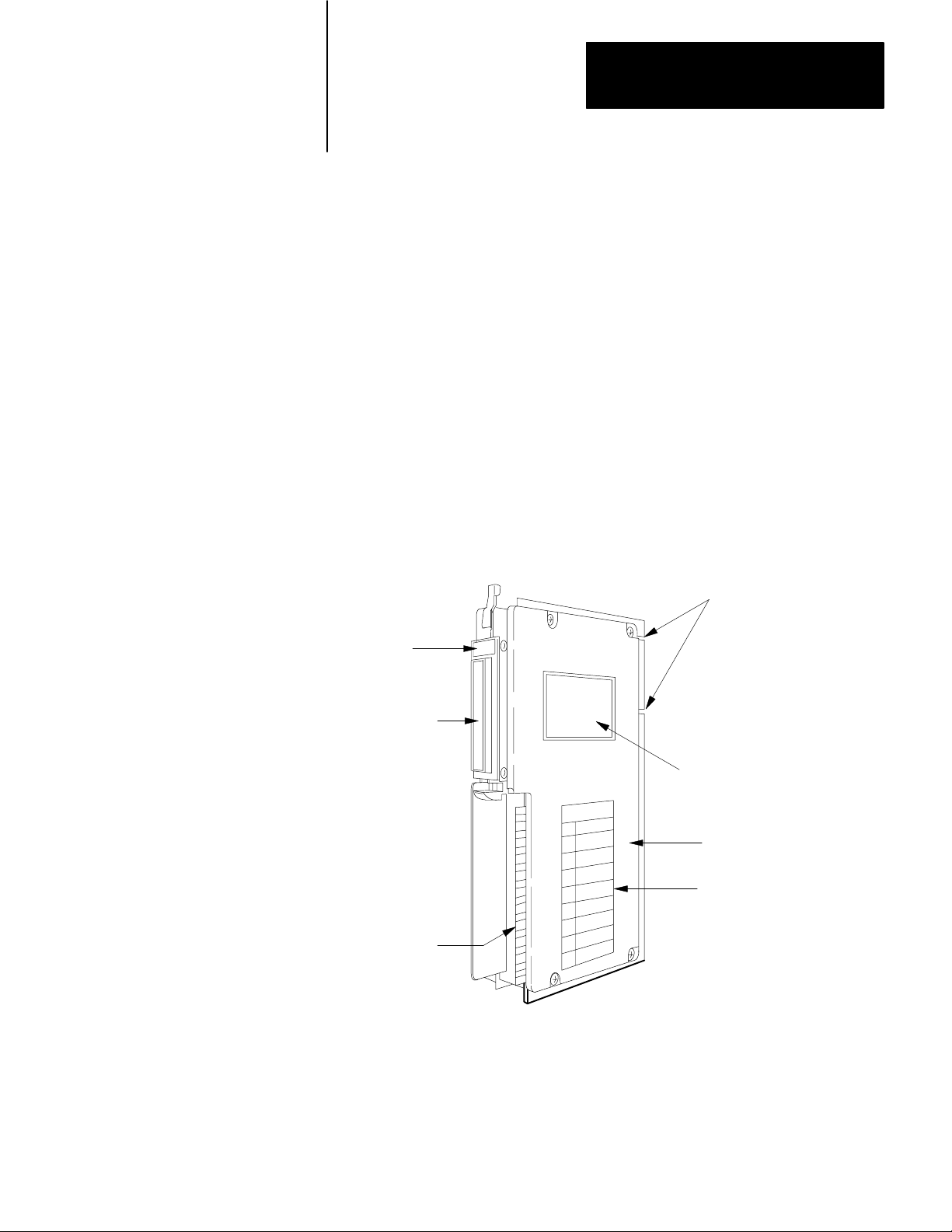
The module (Figure 2.1) senses analog signals at its inputs and converts
these signals to 3-digit Binary Coded Decimal (BCD) values (0 to 255
BCD) for use by your programmable controller.
Figure 2.1
Input Module
Analog
Keying Slots
Pink
Identification
Label
Range/Calibration
Date Label
Labels Identify Module
Type/Series
Protective
Covers
Label Specif ies
Terminal Connection
Wiring Arm
Connects Here
17996
The module accepts up to eight analog signals having a single voltage or
current range that you select based on the type of input devices required
by your application. It allows your programmable controller to
21
Page 6

Chapter 2
Overview of the Analog Input Module
manipulate values representing temperature, pressure, rotational speed,
light intensity, and position.
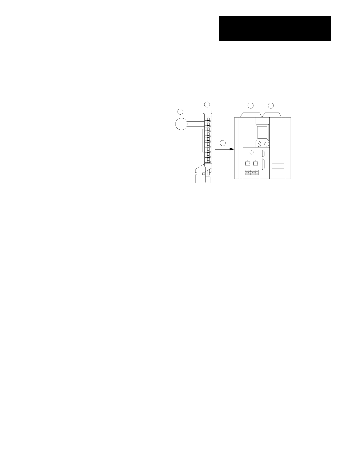
A wiring arm (cat. no. 1771-WB) accompanies the module. It acts as a
terminal strip for input connections. The wiring arm pivots on the I/O
chassis to connect with terminals on the front of the input module. Thus,
the wiring arm lets you quickly connect or disconnect your input wiring
when inserting or removing the input module from the I/O chassis.
The input module meets the requirements of the Instrument Society of
America, Standard S50.1 (1975), “Compatibility of Analog Signals for
Electronic Industrial Process Instruments.”
Input Channels
The input module supports eight single-ended input channels. All eight
channels have the same voltage or current range that you select when
ordering the module. The range is factory set and calibrated.
Nominal
Range:
1 to 5 V
4 to 20mA
0 to 5 V
0 to 20 mA
10 to 10V
20 to 20 mA
0 to 10 V
Precise Range:
1 to 4.9844 V
4 to 19.937 mA
0 to 4.980 V
0 to 19.922 mA
10 to 9.922V
20 to 19.844
mA
0 to 9.96 V
Units/Bit: Order
Code
15.60 mV/bit
0.063 mA/bit
19.53 mV/bit
0.078 mA/bit
78.13 mV/bit
0.156 mA/bit
39.06 mV/bit
01
05
02
06
03
07
04
When ordering 1771-IE modules, place the order code as a suffix to the
catalog number. For example, 1771-IE-04.
You can change from a voltage range to the equivalent current range and
vice versa within limited catagories. For example, from the above table
you can switch from a range of (1 to 5 VDC) to (4 to 20 mA) or (0 to 5
VDC) to (0 to 20 mA) without recalibrating.
How Analog Modules
Communicate With
Programmable Controllers
22
Analog input modules communicate with a programmable controller by
block transfer in the following manner (Figure 2.2).
Page 7
Chapter 2
Overview of the Analog Input Module
Figure 2.2
Communication
Between Input Module and Processor
2
1
Input
Device
8- BIT Input Module
(cat.no.1771-IE)
3
BTR
4 5
PC Processor
(PLC2/30 Processor
Shown)
14164
1. Input devices generate analog signals which are transmitted to the
input module.
How the Input Module Converts
Analog Signals
2. The input module converts analog signals into BCD values and
stores them until the processor requests a transfer of data.
3. When instructed by your ladder diagram program, the processor
performs a read block transfer of the values and stores them in its
data table.
4. Your program can determine that the transfer was made without
error, and that the values are within a specified range.
5. Your program can use and/or move the data before it is written over
by the transfer of new data in a subsequent block transfer.
The input module converts analog signals to digital values readable by
your processor (Figure 2.3).
The input module scans its inputs every 2.5ms and converts analog data to
a digital format. It stores this data momentarily until transferred to the
processor’s data table. The module reserves the last 200 microseconds of
23
Page 8
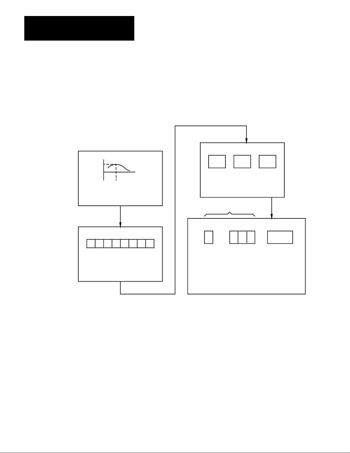
Chapter 2
Overview of the Analog Input Module
each input scan for formatting data, and cannot accept block transfers
during this time.
Figure 2.3
Conversion and Formatting
Input
129
Measurement of analog
voltage or current value
10000001
(129)
Converted to a
binary value
0001 0010
(1) (2) (9)
Converted to
a BCD value
Status added by the module
17 16 - 14 13 - 0
Over/
Under
flow
Channel
number
Stored in memory
1001
(129)
Analog
value
(BCD)
14159
Input Data Format
24
Input data is transferred to the processor in 12-bit 3-digit BCD format
with a range of 0-255.
The processor stores the data in 16-bit input words (Figure 2.4). The 16
bits are used as follows:
Page 9
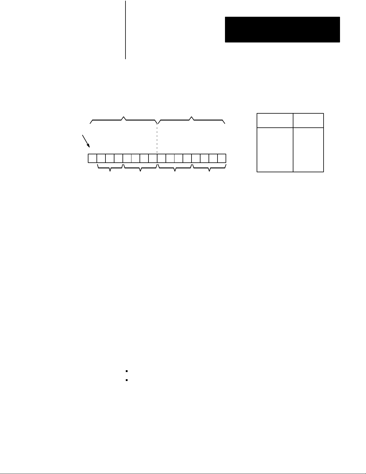
Figure 2.4
Input W
Analog
Chapter 2
Overview of the Analog Input Module
ord
Overflow/
Underflow Bit
High Byte Low Byte
0 = within range
1 = out of range
17 16 15 14 13 12 11 10 07 06 05 04 03 02 01 00
00
Channel
Address
(see table)
Most
Significant
Digit
(0-2)
Middle
Digit
(0-9)
Least
Significant
Digit
(0-9)
Bits 00-11 These bits contain input values which range from 0 to 255
BCD (8 bit resolution).
Channel Address Codes
Bits
16 15 14
0 0 0
0 0 1
0 1 0
0 1 1
1 0 0
1 0 1
1 1 0
1 1 1
Channel
Number
1
2
3
4
5
6
7
8
14165
Bits 12-13 These bits must remain reset (to 0) for proper operation.
Bits 14-16 These bits indicate by binary code which channel is being
read.
Bit 17 This bit indicates an overflow/underflow condition, and is set (to 1)
under the following conditions:
input value is zero or negative
input value is greater than or equal to 255
25
Page 10

Chapter 2
Overview of the Analog Input Module
Specifications
Inputs
Per Module
8 singleended
Humidity Rating
5 to 95% (noncondensing)
Input Voltage Ranges (nominal)
1 to 5 V
0 to 5 V
0 to 10 V
10 to 10 V
Input Current Ranges (nominal)
0 to 20 mA
4 to 20 mA
20 to 20 mA
Input Overvoltage Protection
+
35 VDC
25 VRMS (sinusoidal)
Input Overcurrent Protection
+
30 mA
Input Impedance
10
10
Ohms
for voltage ranges
250 Ohms (+
0.1%) for current ranges
ElectricalOptical Isolation
between input circuit and control
logic: 1500 V
Backplane Current Requirement
400 mA at 5 VDC
Keying (between)
4 and 6
26 and 28
A/D Converter T
ype
successive approximation, monotonic
Resolution
1 part in 256 (28)
Linearity
+
0.1% of full scale at 25o C
Offset
0.15% of full scale at 25o C
+
Gain
0.15% of full scale at 25o C
+
Quantizing Error
+
1/2 LSB (0.19% of full scale)
Absolute Accuracy (including linearity
and gain at 25
o
C)
of full scale +
0.3%
1/2 LSB
Stability (drift over the full temperature
range)
temperature coef
ficient = +
85 ppm/oC
of full scale
, offset,
26
Ambient T
emperature Rating
operating: 0 to 60
(32 to 140oF)
storage 40 to 85oC
(40 to 185oF)
o
C
Inaccuracy (due to internal electrical noise)
3 sigma noise 0.2% RMS of full scale
Page 11

Chapter
3
Installing the Analog Input Module
Chapter Objectives
Before You Install the Input Module
This chapter gives you information on:
choosing an external power supply
wiring the input module’s field wiring arm
keying a chassis slot for your module
setting internal configuration switches
installing the input module
The input module is shipped to you configured for block transfer
operation. If you want to use single transfer, see Appendix C for proper
switch settings.
Before installing your input module in the I/O chassis you should:
1. Calculate the power requirements of all modules in each chassis. See
“Power Requirements.”
2. Determine where to place the module in the I/O chassis. See
“Module Location in the I/O Chassis.”
Electrostatic Damage
3. Key the backplane connector in the I/O chassis. See “Keying.”
4. Make connections to the wiring arm. See “Wiring” and
“Grounding.”
5. Set configuration switches (only if you want single transfer, or to
change to the alternate input range).
Electrostatic discharge can damage semiconductor devices inside this
module if you touch backplane connector pins, or when you set
configuration plugs or switches inside the module. Guard against
electrostatic damage by observing the following precautions:
31
Page 12
Chapter 3
Installing the Analog Input Module
Touch a grounded object to rid yourself of elctrostatic charge before
handling the module.
Handle the module from the front, away from the backplane connector.
Do not touch backplane connector pins.
When setting internal switches or configuration plugs, do not touch
semiconductor devices inside the module. Use a static-safe work
station if available.
Keep the module in its static-shield bag when not in use.
CAUTION: Electrostatic discharge can degrade performance
or cause permanent damage. Handle this module as stated
above.
Power Requirements
Your module requires 400 mA from the I/O chassis backplane. Calculate
the power usage of all modules in the I/O chassis so you do not exceed the
power rating of the chassis backplane or the backplane power supply.
The input module also requires an external power supply exclusively for
analog modules. Using a separate supply protects the analog signal from
transients caused by the switching of digital circuits. The specifications
for the external DC power supply are:
Specifications 5V 15V 15V
current
per input module
voltage tolerance
regulation (type)
line regulation
(for 10 VAC RMS input change)
load regulation
150mA 70mA 70mA
1% 1% 1%
linear
(series or
shunt)
.02% .02% .02%
.04% .02% .02%
linear
(series or
shunt)
linear
(series or
shunt)
32
ripple
overvoltage protection
current limit
(% of full load)
1 mV 1 mV 1 mV
7 V
125% 125% 125%
18 V
18 V
Page 13

Chapter 3
Installing the Analog Input Module
We recommend either of two Allen-Bradley power supplies:
Power Supply (cat. no. 1770-P1) provides sufficient current for two
1771-IE input modules. This supply operates on either 120 or 220/240
VAC.
The Remote Power Supply (cat. no. 1778-P2) provides external power
for up to ten 1771-IE input modules. Do not use this supply for I/O
chassis power when powering analog modules. We recommend that you
order one or two power cables (cat. no. 1771-CF), and connect no more
than five 1771-IE input modules with a single power cable.
Power and common connections can be jumpered from one 1771-IE input
module to the next. Be careful to minimize the voltage drop in your
power connections.
Module Location
Keying
WARNING: Maintain at least 5.0 VDC between the 5 VDC
terminal and common terminal measured at the wiring arm. A
lower voltage could cause intermittent operation resulting in
possible damage to equipment and personal injury.
Place your module in any I/O module slot except for the extreme left slot
of the I/O chassis. This slot is reserved for PC processors or adapter
modules. We recommend the following:
Do not put this input module in the same module group with a discrete
high density I/O module when using 2-slot addressing because this
input module uses both the input and output image tables for block
transfer. Two analog input modules, however, may be put in the
same module group.
Group analog input modules away from AC or high voltage DC I/O
modules to minimize electrical noise interference.
Once you designate a slot for your input module, you should not place
other types of modules in this slot. We recommend that you use the
keying bands, shipped with your I/O chassis, to accept only one type of
module in a designated I/O slot.
33
Page 14
Chapter 3
Installing the Analog Input Module
To key a module slot to accept only the 1771-IE module, position the
keying bands on the upper backplane connector at the following positions
(Figure 3.1):
between 4 and 6
between 26 and 28
Figure 3.1
Positions
Keying
2
4
6
8
10
12
Keying
Bands
14
16
18
20
22
24
26
28
30
32
34
36
14169
Wiring
34
Connect analog devices and external power to your input module through
the Field Wiring Arm (cat. no. 1771-WB). The wiring arm pivots on the
front of the I/O chassis to connect with the module. Wiring connections
are made at the wiring arm, so you can remove the module from the
chassis without disconnecting the wiring.
Connection diagram (Figure 3.2) shows connections of analog devices
and power supply to the wiring arm of the input module.
The COMMON terminal on the wiring arm connects to the power supply
COMMON and SIGNAL RETURN wires from each of your input
devices (Figure 3.2). Do not confuse the SIGNAL RETURN wire with
the cable shield. The SIGNAL RETURN is one of the insulated wires of
the cable-twisted pair. The cable shield is discussed in the next section.
When wiring analog devices to the wiring arm, use Belden No. 8761 or an
equivalent cable. We recommend that the cable from voltage mode input
devices does not exceed 50 feet in length. We base this recommendation
on considerations of noise immunity in typical industrial environments.
Page 15

Chapter 3
Installing the Analog Input Module
There is no restriction on cable length for current mode input devices.
Cable length resistance, however, when added to module input resistance,
must not be enough to cause an overload on the analog driving device.
Figure 3.2
Connection
Diagram
(See application codes and laws.)
+5V
1
2
3
4
5
6
7
8
9
10
11
12
+5-15+15DC
Use
power
supply
Ground cable shield at one end only,
preferably at chassis mounting bolt.
COMM
Analog
signal
source
Chassis
ground mounting
bolt
14168
Channel 1
Channel 2
Channel 3
Channel 4
Channel 5
Channel 6
Channel 7
Channel 8
Supply Comm/
Sig. Rtn.
+15V
-15V
Field Wiring Arm
(Cat. No. 1771-WB)
If you use a 1770-P1 power supply for your external power source, you
must jumper the 5 VDC COMMON and the 15 VDC COMMON
terminals together either at the power supply or at the module. Figure 3.3
shows the wiring connections for the Power Supply (1770-P1).
35
Page 16

Chapter 3
Installing the Analog Input Module
Figure 3.3
Supply Connections (cat. no. 1770P1)
Power
Jumper Positions
For 120V AC
- 15V DC
+ 15V DC
L1
+
15V DC Common
-
L2
+ 5V DC
+ 5V DC Common
Jumper Both Commons
14167
If you use the 1778-P2 remote power supply, connect it to the wiring arm
using one or two power cables (Figure 3.4).
36
Figure 3.4
Supply Connections (cat. no. 1778P2)
Power
7
DC Common
+ 15V
- 15V
+ 5V
Field Wiring Arm for
Analog Input Module
8
9
10
11
12
Red or Blue
Violet
Yellow
Black or Orange
Analog Power able
(Cat. No. 1770CF)
Remote Power Supply
(Cat. No. 1778P2)
Interlock
I/O
I/O
Wiring for power cable (cat. no. 1770CF
is described in publication 17702.25)
14166
Page 17

Chapter 3
Installing the Analog Input Module
Grounding
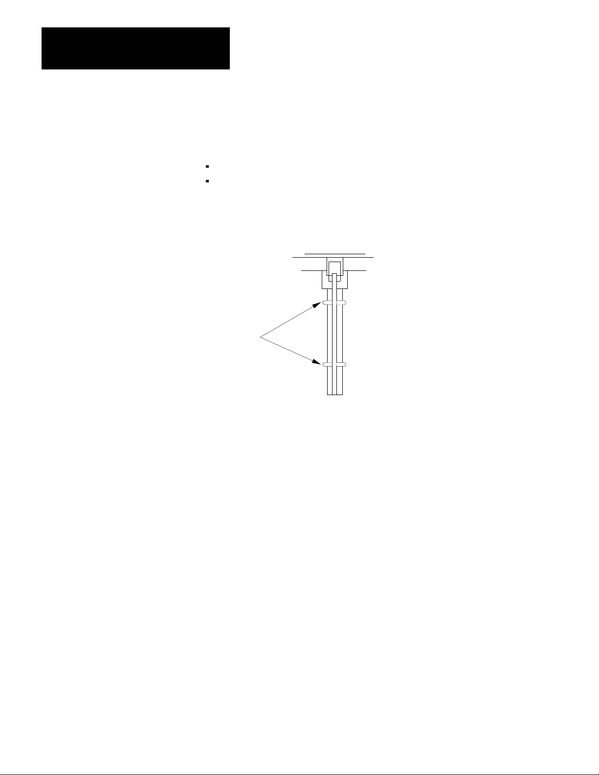
Ground the drain wire and shield of the Belden No. 8761 or equivalent
cable (Figure 3.5) at one end of the cable only. Twist the drain wire and
shield into a single strand. The best ground for this connection is an I/O
chassis mounting bolt or stud.
Insulate the shield and drain wire at the other end of the cable using
electrical tape.
You may mount a separate terminal near the input module for DC
COMMON and SIGNAL RETURN wires. This terminal should be
mounted as close to the module as possible to minimize the length of
unshielded wire.
Refer to Wiring and Grounding Guidelines, publication 1770-4.1 for
additional information.
Figure 3.5
Grounding
the Cable Shield
Ground Shield at
I/O Chassis
Mounting Bolt
Shield and Drain
Twisted into
Single Strnd
Field Wiring Arm
Belden No. 8761
or Equivalent Wire Cable
Refer to the connection diagram for eact twistedpair terminal connections.
17798
37
Page 18

Chapter 3
Installing the Analog Input Module
Setting Configuration Switches
The module is set for block transfer operation andcalibrated at the factory
for the voltage or current range that you ordered.
CAUTION: Electrostatic discharge can degrade performance
or cause permanent damage to the module. Follow the
guidelines on electrostatic discharge located at the beginning of
this chapter before handling the module.
Transfer Mode
You should change the mode of operation to single transfer if your
processor is one of the following:
PLC (now obsolete)
Mini-PLC-2 (cat. no. 1772-LN1, -LN2)
Refer to Chapter 5, “Setting These Switches,” for setting the Transfer
Mode switch to single transfer.
Installing the Input Module
Signal Mode
Without recalibrating, you can change the 1 to 5 VDC or the 0 to 5 VDC
input voltage range to its corresponding 4 to 20 mA or 0 to 20 mA current
range. Refer to Calibration, chapter 5, for the location of the signal mode
switch assembly (Figure 5.1). Set all switches to the same setting as
follows:
If your module is calibrated for one of these two voltage ranges and you
want to change to the corresponding current range: set all switches ON.
If your module is calibrated for one of these two current ranges and you
want to change to the corresponding voltage range: set all switches OFF.
Changing to any other input range requires that you recalibrate your
module to obtain accurate operation.
Now that you have determined the power requirements, location, keying,
wiring, and grounding for the input module, you are ready to install it in
the chassis. Use the following procedure:
38
Page 19

Chapter 3
Installing the Analog Input Module
1. Turn off power to the I/O chassis.
WARNING: Remove power from the 1771 I/O chassis
backplane and wiring arm before removing or installing an I/O
module.
Failure to remove power from the backplane could cause
injury or equipment damage due to possible unexpected
operation.
Failure to remove power from the backplane or wiring arm
could cause module damage, degradation or performance, or
injury.
2. Insert your module into the chassis. Plastic tracks on the top and
bottom of the slots guide the module into position. Do not force the
module into the backplane connector, but apply firm even pressure.
3. Snap the I/O chassis latch over the module. This secures the module
in place.
4. Connect the wiring arm to the module.
5. Turn on power to the I/O chassis.
39
Page 20

Chapter
4
Programming the Analog Input Module
Chapter Objectives
Block Transfer Programming
In this chapter we describe a general block transfer program, and present a
programming example for each family of programmable controllers.
Program your processor to transfer data from the module to the
processor’s data table using a block transfer read (BTR) instruction. We
give you programming examples. Because every application is different,
we urge you not to copy examples but to use the appropriate example as a
guide.
Block transfer programming using the BTR instruction is covered in this
chapter for most PLC-2 family processors, all PLC-3 family processors,
and the PLC-5/15 processor. Other programs for transferring data are
found as follows:
Processor Method Appendix
MiniPLC2
no. 1772LN3)
(cat.
PLC2/20
(cat. no. 1772LP1, LP2)
Block T
ransfer,
Multiple GET
A
General Example
PLC
(cat. no. 1774LB2, LC2)
We assume that you know how to enter ladder diagram programming via
your programming terminal, how to enter instruction parameters, and how
to map your data table or data files for proper data storage. If not, refer to
the manuals that came with your processor. If necessary, refer to
Publications Index, SD499, which lists all publications of the Industrial
Computer Group.
We describe programming rungs in one general example applicable to
most PLC-2 family processors (Figure 4.1). Although instruction formats
are different, the program is also applicable to all PLC-3 family
processors, and the PLC-5/15 processor. We also present an example for
each processor family with specific addresses to show relationships
Single T
ransfer B
41
Page 21

Chapter 4
Programming the Analog Input Module
between instructions. Do not copy these examples. They are for
instructional purposes only.
Figure 4.1
Example
Rung 1
Rung 2
ReadOnly Block T
BTR
DN
ransfer Program
BLOCK XFER READ
DATA ADDR:
MODULE ADDR:
BLOCK LENGTH:
FILE:
FILE TO FILE MOVE
COUNTER ADDR:
POSITION:
FILE LENGTH:
FILE A:
FILE R:
RATE PER SCAN:
EN
DN
EN
DN
PLC2 Family Example
42
Rung 1 This rung uses the BTR instruction to transfer data to the
processor. It transfers data on alternate scans unless you condition it with
instructions that enable it less often.
Rung 2 This rung moves transferred data to a storage location unless old
data was not updated by a new transfer (BTR done bit not set).
Important: Each input word contains an overflow- underflow bit (bit 17)
that your program should monitor to be sure the value is within range.
The module sets this bit when it detects data at or beyond the limits of 0
and 255. We leave this programming logic to you because it is
application dependent.
This example is written for the following conditions (Figure 4.2).
The module resides in rack 1, module group 2, slot 0 8-word block
transfer
Page 22

BTR data (control) address is 030
BTR file address is 050
FFM counter address is 043
FFM number of words moved
is 8
FFM source file A is 050
FFM destination file R is 150
FFM rate per scan is 8
Chapter 4
Programming the Analog Input Module
Figure 4.2
Example
Rung 1
Rung 2
Rung 3
Program for PLC2 Family Processors (Local Chassis)
BLOCK XFER READ
DATA ADDR:
MODULE ADDR:
BLOCK LENGTH:
FILE:
BTR
DN
112
07
Use only when 1771-IE is in a local chassis and block transfers to this
module are inhibited.
FILE TO FILE MOVE
COUNTER ADDR:
POSITION:
FILE LENGTH:
FILE A:
FILE R:
RATE PER SCAN:
030
120
050 - 057
043
050 - 057
150 - 157
08
000
08
08
012
EN
07
112
DN
07
043
EN
17
043
DN
15
012
IOT
Important: When your input module is in a local I/O chassis, random
chance could allow block transfer requests to occur during module
housekeeping and prevent block transfers. This condition is apparent
when the done bit remains reset and no new data is transferred. If this
condition should occur, we recommend that you add rung 3 to your
program. It guards against the possibility of the processor repeatedly
asking for a block transfer each time the module inhibits block transfers
while updating its inputs.
43
Page 23

Chapter 4
Programming the Analog Input Module
This rung adds up to 0.13ms to the processor scan time so use it sparingly.
Locate it at the beginning of your ladder program. This logic is not
required for PLC-2 family remote systems or for any other processor
family.
PLC3 Family Example
This example is written for the following conditions (Figure 4.3).
The module resides in rack 1, module group 2, slot 0
8-word block transfer
BTR control address is FB001:0000
BTR file address is FB002:0001
MVF source file A is FB002:0001
MVF destination file R is FB003:001
MVF counter address is C000l
MVF number of words moved is 8
MVF rate per scan is all/scan
Figure 4.3
Example
Program for PLC3 Family Processors
WB001:0000
(DN)
15
BTR
BLOCK TRANSFER READ
RACK :
GROUP :
MODULE :
DATA :
LENGTH =
CNTL :
FB002:0001
FB001:0000
001
0=LOW
CNTL
LE
12
2
CNTL
DN
15
8
CNTL
ER
13
44
WB001:0000
(DN)
15
MVF
FILES FROM A TO R
A :
R :
COUNTER :
POS/LEN =
MODE=
FB002:0001
FB003:0001
ALL/SCAN
C0001
C0001
EN
12
C0001
DN
8
15
C0001
ER
13
Page 24

Chapter 4
Programming the Analog Input Module
PLC5/15 Example
This example is written for the following conditions (Figure 4.4).
The module resides in rack 1, module group 2, slot 0 8-word block
transfer
BT Array (integer control address) is $N7:51
Data file (integer file address) is $N7:56
Figure 4.4
Example
Program for the PLC5/15 Processor
$N7:51
EN
BTR
BLOCK TRANSFER READ
RACK :
GROUP :
MODULE :
BT ARRAY
DATA FILE:
LENGTH:
CONTINUOUS
1
2
0
$N7:51
$N7:56
8
N
EN
15
DN
13
ER
12
Programming Considerations
Important: The PLC-5/15 processor buffers read block transfer data
automatically, so program buffering is not required.
We suggest that you follow programming considerations applicable to
your programmable controller. They are listed below and described in the
manual that accompanied your controller.
PLC2 Family
Determine the first available block transfer address in the timer and
counter area of the data table. For PLC-2/20 and PLC-2/30 processors,
it depends on the number of assigned remote I/O rack numbers.
Leave unused addresses following your last block transfer address for
future block transfer instructions.
Load zeros into the address following the last (reserved) block transfer
address to establish a boundary that prevents the processor from
looking further for additional block transfer addresses.
Buffer incoming (BTR) data. Be sure it is valid before using it.
Examine the BTR done bit and any other status bit that monitors its
validity.
45
Page 25

Chapter 4
Programming the Analog Input Module
PLC3 Family
If your application requires many block transfer modules, distribute the
modules over as many I/O chassis as possible to optimize transfer time
for the system as a whole.
Where allowed by your application, program block transfers to occur
less often than once per program scan.
Buffer incoming (BTR) data. Be sure it is valid before using it.
Examine the BTR done bit and any other status bit that monitors its
validity.
PLC5/15
Incoming (BTR) data is buffered automatically by the processor.
46
Page 26

Chapter
5
Calibrating the Analog Input Module
Chapter Objective
Service Information
Calibration Equipment
This chapter describes how you calibrate the module.
Your input module is calibrated at the factory. We recommend that you
recalibrate it every year to maintain accuracy. If for some reason you can
not calibrate the module, return it to Allen-Bradley Company for
recalibration. The mailing address is:
Allen-Bradley Company
Industrial Computer Group
747 Alpha Drive
Highland Heights, Ohio 44143
We recommend the following equipment for calibrating the module:
Equipment: Description/Source:
precision
source
digital voltmeter
sealant T
alignment tool
industrial terminal
voltage
+10V
, 0.1mV resolution minimum
Analog 3100, Data Precision 8200, or equivalent
5 1/2 digit, 0.01% accuracy minimum
Keithley 191, Fluke 8300A, or equivalent
orque Seal" by Organic Products or equivalent
P/N 35F616, for potentiometer adjustment,
Newark Electronics or equivalent
cat. no. 1770T3 with cable (cat. no. 1772TC) for
PLC2 family processors
cat. no. 1770T4 with cable (cat. no. 1775CAT) for
PLC3 family processors
cat. no. 1784T50 for PLC5/15 processors
51
Page 27

Chapter 5
Calibrating the Analog Input Module
Before You Calibrate
Before you calibrate, follow these steps:
1. Turn OFF power to the I/O chassis backplane and to your wiring
arm.
WARNING: Remove power from the 1771 I/O backplane and
wiring arm before removing or installing an I/O module.
Failure to remove power from the backplane could cause
injury or equipment damage due to unexpected operation.
Failure to remove power from the backplane or wiring arm
could cause module damage, degradation of performance, or
injury.
2. Disconnect all analog signal inputs from the module’s wiring arm
(leave 5V, +
15V DC, and COMMON connections attached). Label
the inputs to aid you in reconnection.
Calibrating the Input Module
3. Remove the module from the chassis by pivoting the wiring arm
down and releasing the plastic lever at the top of the module. Pull
the module straight out from the slot.
CAUTION: Electrostatic discharge can degrade performance or
cause permanent damage. Refer to the guidelines at the
beginning of chapter 3.
4. Remove screws from the four corners of each cover plate and
remove the covers. This gives you access to internal switch
assemblies.
Connect your industrial terminal to your processor so you can display
channel input values in BCD during calibration. Be sure your processor is
programmed to block transfer data from the module. For safety purposes,
disable all outputs or disable your ladder program except for transferring
data from the module you are calibrating.
52
To calibrate the module, you
Page 28

set internal switches
adjust the offset (Part A)
adjust the offset (Part B)
calibrate the gain
Chapter 5
Calibrating the Analog Input Module
Setting the Switches
There are three sets of switch assemblies (Figure 5.1) in the module:
Range Select
Signal Mode
Transfer Mode
Figure 5.1
Location
of Switch Assemblies
Transfer
Mode
Range
Select
Signal
Mode
14162
53
Page 29

Chapter 5
Calibrating the Analog Input Module
Set these switches as follows:
1. Range Select switch assembly lets you select a current or voltage
input range by setting switches 1-10. These switch settings remain
the same during and after calibration.
Change these switch settings only if you want to change to another
voltage or current input range group.
Range: Switch
1 2 3 4 5 6 7 8 9 10
1 to 5V
4 to 20 mA
0 to 5V
0 to 20 mA
0 to 10V
+10V ON ON OFF OFF ON OFF ON OFF ON OFF
+20mA ON ON OFF OFF ON OFF ON ON OFF OFF
OFF
OFF
ON
ON
ON ON OFF OFF ON ON OFF ON OFF OFF
OFF
OFF
ON
ON
ON
ON
OFF
OFF
ON
ON
OFF
OFF
OFF
OFF
ON
ON
Number
ON
ON
ON
ON
OFF
OFF
OFF
OFF
ON
ON
ON
ON
OFF
OFF
OFF
OFF
OFF
OFF
ON
ON
2. Signal Mode switch assembly lets you select current mode (all
switches are ON) or voltage mode (all switches are OFF).
CAUTION: Be sure external power (15, 5 VDC) is OFF before
changing the signal mode switch.
Set all eight switches to OFF (voltage mode) during calibration.
Offset (Part A)
54
3. Transfer Mode switch assembly lets you select single transfer (switch
1 ON) or block transfer (switch 1 OFF).
Change the setting of switch 2 to ON only for the Offset (Part A)
procedure.
This procedure applies only if your input range is (1 to 5 VDC) or (4 to 20
mA).
Important: If the input range of your module is other than a range of (1
to 5 VDC) or (4 to 20 mA), skip this procedure and go directly to Offset
(Part B).
Page 30

Chapter 5
Calibrating the Analog Input Module
Make this adjustment for channel 1, only.
1. Set switch number 2 ON of the transfer mode switch assembly.
2. Place the module back in its I/O slot, and connect the wiring arm.
3. Change the processor mode select switch to test or program mode.
Turn on power to the processor, I/O chassis, and external power
supply to the module.
4. Connect the precision voltage source:
positive lead to input channel 1
negative lead to DC COMMON of the wiring arm
5. Turn on the precision voltage source and set it to 1.0000 Vdc.
6. Connect the DVM leads to the test points on the front of the module,
positive lead to the red test point, negative lead to the black test
point.
7. Read the voltage at the test points. It must be 0.0000 0.2 mV. If not,
adjust potentiometer #1 on the front of the module (Figure 5.2).
55
Page 31

Chapter 5
Calibrating the Analog Input Module
Figure 5.2
Location
of Potentiometers and T
est Points
Potentiometer #1
Potentiometer #2
Potentiometer #3
Red Test Point
Black Test Point
14163
Offset (Part B)
8. Seal the setting with a drop of sealant.
9. Turn off power to the external power supply, I/O chassis, and
processor.
10. Remove the module from the I/O chassis.
11. Reset switch number 2 OFF of the transfer mode switch assembly.
12. After replacing the covers, place the module back in its slot in the
I/O chassis.
Start your calibration procedure here if your input range is NOT (1 to 5
VDC) or (4 to 20 mA).
You make one adjustment for all channels at the same time for offset, then
one adjustment for gain calibration.
56
Page 32

Chapter 5
Calibrating the Analog Input Module
1. Jumper all 8 input terminals together at the wiring arm.
2. Connect the precision voltage source to the jumpered input terminals
and to ground.
3. Set the precision voltage source to the input value required for
minimum output for your particular input range. Remember that you
set the module to operate in voltage mode for calibration.
Range Input
1 to 5 V
0 to 5 V
10 to 10 V
0 to 10 V
for Minimum Output
1.0078 V
0.0098 V
9.9609 V
0.0195 V
4. Observe the BCD value. It should toggle between 000 and 001 for
equal lengths of time. If not, adjust potentiometer #2.
Do not seal the potentiometer until you have finished adjusting the gain.
Gain
5. Set the precision voltage source to the input value required for
maximum output for your particular input range. Remember that
you set the module to
Range Input
1 to 5 V
0 to 5 V
10 to 10 V
0 to 10 V
for Maximum Output
4.9766 V
4.9707 V
9.8828 V
9.9414 V
6. Observe the BCD value. It should toggle between 254 and 255 for
equal lengths of time. If not, adjust potentiometer #3.
7. Recheck offset and gain to be sure that they are properly set. Adjust
if necessary.
8. Seal the potentiometers.
57
Page 33

Chapter 5
Calibrating the Analog Input Module
9. If your input range was a current range, reset the signal mode switch
assembly to current mode (all switches on).
10. Re-install and test the module with known values before operating
with I/O devices.
58
Page 34

Appendix
A
Block Transfer (Multiple GET) for PLC2/20
Example Program
Assumptions
This read-only program (Figure A.1) transfers a block of input data from
the analog input module to a momentary storage (buffer) in the
processor’s data table. If valid, input data is moved elsewhere in the data
table for use by your ladder program. If invalid, it is written over by the
next block transfer. This program performs the same function as the
2-rung program described in chapter 4.
Important: If you place your input module in a local chassis, we
recommend that you add the same rung as described in the PLC-2 family
example (Figure 4.2, Rung 3). This rung guards against the possibility of
the processor repeatedly asking for a block transfer when the module
momentarily inhibits block transfers while updating its inputs.
The example program is based on the following assumptions:
module in rack 1, module group 2, slot 0
8-word block transfer
block transfer (control) address 030
read block transfer (buffer) file 050-057
storage file 150-157
A1
Page 35

Appendix A
Block Transfer (Multiple GET) for PLC-2/20
Figure A.1
Example
Rung 1
Rung 2
Rung 3
Rung 4
Rung 5
Rung 6
Rung 7
Rung 8
Rung 9
Rung 10
Rung 11
Rung 12
Rung 13
Rung 14
Rung 15
Rung 16
Rung 17
Rung 18
Program for PLC2/20
Ladder Diagram Dump
02000 11207
Block Length
030 130
GG
120
050
01207
02002
02002
02002
02002
02002
02002
02002
02002
050
G
000
1
050
G PUT
000
051
G PUT
000
052
G PUT
000
053
G PUT
000
054
G PUT
000
055
G PUT
000
056
G PUT
000
057
G PUT
000
052
051
G
G
000
000
2345
Start
Clears Block Transfer Flag
Block Transfer
Block Transfer Flag
Moves Data
053
054
055
G
G
G
000
000
000
678
056
G
000
057
G
000
02002
02000
U
01200
U
01201
U
01202
U
01203
L
01204
U
01205
U
01207
02000
L
ON
150
1
000
151
2
000
152
3
000
153
4
000
154
5
000
155
6
000
156
7
000
157
8
000
Display
Only
A2
Page 36

Appendix A
Block Transfer (Multiple GET) for PLC-2/20
Description
Scan 1
Rung 9
This rung controls block transfer. Preconditions are optional. The first
available word 030 in the timer/counter accumulated area stores module
location 120. Word 130 in the timer/counter preset area stores the address
of the first word in the BTR (buffer) file.
Output bit 01207 initiates block transfer. The first digit of this output
address is zero, because it is in the output image table. The next three
digits are the module’s location: rack, module group, and slot numbers.
The last digit, 7, is the BTR enable bit (bit 17 if the module was in slot 1).
Rung 10
Bit 01207 is examined to determine if a block transfer was initiated. If
initiated, Bit 02000 is latched until the next program scan.
Scan 2
Rung 1
This rung detects the request (02000) and completion (11207) of a block
transfer to this module. Upon completion, it lets transferred data move to
storage location words 150-157 in rungs 11-17.
Rung 2
This rung resets the block transfer operation. Bit 02000 is unlatched. It
will be latched again if a block transfer request is made this program scan.
Rungs 3 7
These rungs determine the block length by setting a binary code equal to
the number of words transferred.
A3
Page 37

Appendix A
Block Transfer (Multiple GET) for PLC-2/20
Rungs 11 18
These rungs move data from the BTR read file to storage. When the
block transfer one-shot (02002) is set, data in each (buffer) word address
050-057 is moved to storage location 150-157 where it can be used by
your ladder program. If data is not moved, it is written over by the next
block transfer.
Important: Each input word contains an overflow- underflow bit (bit 17)
that your program should monitor to be sure the value stored in that word
is within range. The module sets this bit when it detects data at or beyond
the limits of 0 and 255. We leave this programming logic to you because
it is application dependent.
Last Rung
These GET instructions display the BCD value of each transferred word,
and are for display only.
A4
Page 38

Appendix
B
Single Channel Transfer for PLC Processors
Example Program
Programming techniques used in this example program (Figure B.1) for
the PLC processor include:
I/O scan counter
conditional ignore zone
I/O Scan Counter
The I/O scan counter (rungs 1-3) controls the transfer sequence and gives
the module sufficient time to respond to channel byte and update select
commands.
The scan counter increments only when a program scan and I/O scan have
occurred. It does this by manipulating a specially chosen bit. The bit
must be in the input image table, and must have an input module
associated with it. The terminal corresponding to this bit must NOT have
an input device wired to it so it can be turned OFF each I/O scan. Choose
a bit which satisfies these conditions:
It has an input address with the same assigned rack number as the input
module.
The input terminal associated with that bit address should be in a
module group with a higher module group number than the one the
input module is in.
The input terminal associated with that bit address must be unused.
Wire it to DC COMMON or L2 (AC Low) to guard against wiring it to
an input device.
Conditional Ignore Zone
The conditional ignore zone controls multiple output instructions based on
a set of overriding conditions. When these conditions are true, the outputs
within the zone are controlled by the conditions in their individual rungs.
When false, the zone outputs are held in their last state, whether ON or
OFF.
B1
Page 39

Appendix B
Single Channel Transfer for PLC Processor
The rungs within the conditional ignore zone (rungs 6-25) reconstruct and
store the 16-bit input word from each channel. The override condition of
the zone must be true (I/O scan counter accumulated value = 007) for the
state of any output within the zone to be changed.
B2
Page 40

Appendix B
Single Channel Transfer for PLC Processor
Figure B.1
Example
Rung
No.
Program for the PLC Processor
02200 11111
1
20017
2
3
200
365
005
365
005
367
007
110
=
G
000
=
=
4
G
000
200
5
G
000
200
6
G
000
200
7
G
000
25100 25010
8
200
CTU
PR 007
AC 000
11111
20017
250
PUT
000
01007
L
37710
251
PUT
000
L
/
L
Scan counter
Store low byte
Latch high byte
select
Begin
condiional
ignore zone
Store high byte
25101 25011
9
25102 25012
10
25103 25013
11
25104 25014
12
25105 25015
13
25106 25016
14
25107 25017
15
25017 25016 25015 25014
16
250
G
000
360
=
000
02002
Reconstruct
channel
upper byte
bit-by-bit
Fault
diagnostic rung
B3
Page 41

Appendix B
Single Channel Transfer for PLC Processor
22
23
24
25
26
27
28
29
30
31
B4
02002 250
17
18
19
20
21
01000 01001 01002 01003 01004 01005 01006
02002 01000
02002 01001
02002 01002
02002 01003
02002 01004
02002 01005
02002 01006
200
G
000
200
G
000
200
G
000
203
G
000
200
G
000
203
G
000
200
G
000
203
G
000
367
007
367
007
367
007
361
001
363
003
362
002
363
003
363
003
250
G
000
250
G
000
250
G
000
250
G
000
250
G
000
250
G
000
250
G
000
=
=
363
=
G
002
=
<
=
<
=
G
000
260
PUT
000
261
PUT
000
262
PUT
000
263
PUT
000
264
PUT
000
265
PUT
000
266
PUT
000
267
PUT
000
37710
U
01007
U
203
CTU
PR =008
AC = 000
200
PUT
000
01000
01001
01002
Channel No.
1
2
3
4
Store
channel
values
5
6
7
8
End
conditional
ignore zone
Unlatch byte
select
Increment
reference
counter
Load Scan
Counter with
002
Update
SELECT
Bits
Channel
SELECT
Bits
Page 42

32
33
34
35
36
203
G
000
203
G
000
203
G
000
203
G
000
203
G
000
02200
364
=
004
365
005
366
006
367
007
370
008
Appendix B
Single Channel Transfer for PLC Processor
Channel
SELECT
01003
=
=
=
=
01004
01005
01006
200
CTR
Bits
Reset
Counters
37
38
203
G
000
260
G
000
370
008
261
G
000
=
262
263
264
265
266
267
G
G
G
G
G
G
END 0400
000
000
000
000
000
000
203
CTR
Display
Rung
B5
Page 43

Appendix B
Single Channel Transfer for PLC Processor
Program Logic
Rung
No.
1-3
29 30
Start
Increment I/O
scan counter
(200)
Is
Scan count
<3?
No
Is Yes
Scan count
= 3?
No
In single channel transfer, the processor transfers data one byte at a time.
Your program must reconstruct the data into 16-bit words in the correct
sequence. We developed a flow chart (Figure B.2) that describes single
transfer programming to help you understand the logic.
Figure B.2
Chart for PLC Example Program
Flow
Yes
1. Store input word (110) containing
high byte.
2. Reconstruct channel word.
3. Check Module fault diagnostics.
4. Store channel word.
5. Reset Byte SELECT bit.
6. Increment Reference Counter (203).
7. Load Scan Counter (200) with 002.
Yes Set Update
SELECT bits
Reset Update
SELECT bits. Set
Channel No. 1
SELECT
command.
(Bits 0-6 of output
byte OFF.)
Is
Scan count
= 7?
No
Set Channel
SELECT bits
Rung
No.
6
7
8-15
16
17-24
26
27
28
29-35
B6
Is No
Scan count
= 5?
4
5
Yes
Store input word
(110) containing
low byte
Set Byte SELECT
bit to 1. (Selects
High Byte.)
Have
all Module
Channels been
Read?
(Does CTU 203
= 8?)
No
To balance of program
Yes
Reset both scan
and reference
counters (200
and 203)
36, 37
14161
Page 44

Appendix B
Single Channel Transfer for PLC Processor
Assumptions
Using Less Than Eight Input Channels
The example program is based on the following assumptions:
The input module is in slot 0 of module group 0 in rack 1.
All eight channels are used. If fewer channels are used, rungs may be
eliminated.
The following data table addresses are used to store values:
- words 250-251 serve as momentary storage
- words 260-267 store input channel values
- words 360-370 store constants 000-008
Often fewer than eight input channels are connected to the module. If
using fewer than eight inputs, omit channels in reverse order. Omit
channel 8 first, channel 7 second, etc, when connecting analog devices
and when programming.
You can shorten the program to conserve memory and decrease program
scan time. To reduce program size, study the sequence of events used to
update module data and to read the data from each channel. Reduce the
program as follows:
Omit channel select bit instructions starting with 10116, 01005, etc.
(rung 17).
Omit rungs that store channel values starting with rung 24, rung 23, etc.
Reduce the byte select comparison value in word 367 (rung 26).
Reduce the preset of the increment reference counter (rung 27).
Program channel select bits only for those channels you are using.
Omit rung 35 for channel 8, rung 34 for channel 7, etc.
Reset counters to the number of channels used by reducing the
comparison value stored in word 370 (rungs 36 and 37) accordingly.
Reduce the number of GET instructions in the display rung (rung 38).
B7
Page 45

Index
A
audience, 11
C
Calibration equipment, 51
Calibration procedure, 52
gain, 57
offset (part A), 54
offset (part B), 56
Communication, module to processor, 23
configuraion switches, 38
Connection Diagram, 35
E
Electrostatic Damage, 31
G
Grounding, 37
L
Location of module, 33
Location of potentiometers, 56
Location of switch assemblies, 53
P
Power requirements, 32
Power supply connections, 36
Programming block transfer, 41
general example, 41
PLC-2 family example, 42
PLC-2/20 (using multiple GET), A1
PLC-3 family example, 44
PLC-5/15 example, 45
Programming considerations, 45
S
Service information, 51
Specifications, 26
Switch assemblies, 53
I
Input channels, 22
Input Data Format, 24
K
Keying, 33
W
Wiring, 34
Page 46

AllenBradley
ductivity and quality for more than 90 years. W
, a Rockwell Automation Business, has been helping its customers improve pro
e design, manufacture and support a broad range
of automation products worldwide. They include logic processors, power and motion control
devices, operator interfaces, sensors and a variety of software. Rockwell is one of the worlds
leading technology companies.
Worldwide representation.
Argentina • Australia • Austria • Bahrain • Belgium • Brazil • Bulgaria • Canada • Chile • China, PRC • Colombia • Costa Rica • Croatia • Cyprus • Czech Republic •
Denmark • Ecuador • Egypt • El Salvador • Finland • France • Germany • Greece • Guatemala • Honduras • Hong Kong • Hungary • Iceland • India • Indonesia •
Ireland
•
Israel • Italy • Jamaica • Japan • Jordan • Korea • Kuwait • Lebanon • Malaysia • Mexico • Netherlands •New Zealand • Norway • Pakistan • Peru •
Philippines
Sweden
AllenBradley Headquarters, 1201 South Second Street, Milwaukee, WI 53204 USA, T
• Poland • Portugal • Puerto Rico • Qatar • Romania • RussiaCIS • Saudi Arabia • Singapore • Slovakia • Slovenia • South Africa, Republic • Spain •
•
Switzerland • Taiwan • Thailand • Turkey • United Arab Emirates • United Kingdom • United States • Uruguay • V
enezuela
• Yugoslavia
el: (1) 414 3822000 Fax: (1) 414 3824444
Publication 1771-6.5.7 - December, 1986
Supersedes 1771-810 - February
Publication 1771-6.5.7 - December, 1986
, 1981
Copyright
1986 AllenBradley Company
PN 955100-45
, Inc. Printed in USA
 Loading...