

Pioneer XV-DV282AP, XV-DV181, XV-DV180, XV-DV585K, XV-DV590K Service Manual
PIONEER CORPORATION 4-1, Meguro 1-chome, Meguro-ku, Tokyo 153-8654, Japan
PIONEER ELECTRONICS (USA) INC. P.O. Box 1760, Long Beach, CA 90801-1760, U.S.A.
PIONEER EUROPE NV Haven 1087, Keetberglaan 1, 9120 Melsele, Belgium
PIONEER ELECTRONICS ASIACENTRE PTE. LTD. 253 Alexandra Road, #04-01, Singapore 159936
PIONEER CORPORATION
2009
PHONES
For details, refer to "Important Check Points for good servicing".
MAIN
USB
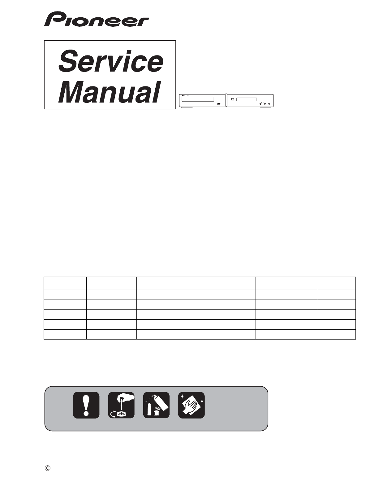
XV-DV282AP
SUBMIC
DVD/CD RECEIVER
XV-DV282AP
XV-DV181
XV-DV180
XV-DV585K
XV-DV590K
THIS MANUAL IS APPLICABLE TO THE FOLLOWING MODEL(S) AND TYPE(S).
ORDER NO.
RRV3936
Model Type Power Requirement Region No. Remarks
XV-DV282AP LXJ AC 220 V to 240 V 3
XV-DV181 LXJ AC 220 V to 240 V 3
XV-DV180 LXJ AC 220 V to 240 V 3
XV-DV585K SXJ5 AC 220 V to 240 V 5
XV-DV590K SXJ5 AC 220 V to 240 V 5
T- Z Z K MAY
2009 Printed in Japan
1
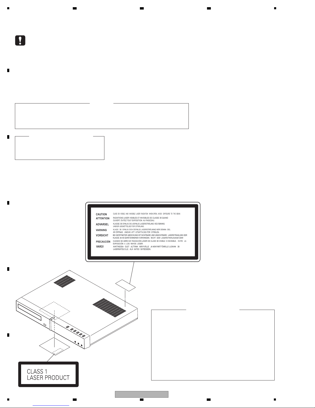
LABEL CHECK
Name label
WARNING !
THE AEL (ACCESSIBLE EMISSION LEVEL) OF THE LASER POWER OUTPUT IS LESS THAN CLASS 1
BUT THE LASER COMPONENT IS CAPABLE OF EMITTING RADIATION EXCEEDING THE LIMIT FOR
CLASS 1.
A SPECIALLY INSTRUCTED PERSON SHOULD DO SERVICING OPERATION OF THE APPARATUS.
LASER DIODE CHARACTERISTICS
FOR DVD : MAXIMUM OUTPUT POWER : 5 mW
WAVELENGTH : 650 nm
FOR CD : MAXIMUM OUTPUT POWER : 5 mW
WAVELENGTH : 780 nm
Additional Laser Caution
∗ : See page 28.
1.
• Laser diode is driving with Q307 (650 nm LD) and Q308
(780 nm LD) on the 08 DVDM Assy.
Therefore, when short-circuit between the emitter and
collector of these transistors or the base voltage is supplied
for transistors turn on, the laser oscillates. (failure mode)
• In the test mode ∗ , there is the mode that the laser oscillates
except for the disc judgment and playback. LD ON mode in
the test mode oscillates with the laser forcibly.
2. When the cover is open, close viewing through the objective
lens with the naked eye will cause exposure to the laser beam.
This service manual is intended for qualified service technicians; it is not meant for the casual
do-it-yourselfer. Qualified technicians have the necessary test equipment and tools, and have been
trained to properly and safely repair complex products such as those covered by this manual.
Improperly performed repairs can adversely affect the safety and reliability of the product and may
void the warranty. If you are not qualified to perform the repair of this product properly and safely,
you should not risk trying to do so and refer the repair to a qualified service technician.
PRW1608
2 3 4
SAFETY INFORMATION
A
B
C
D
E
F
2
1
XV-DV282AP
2 3 4
5
[Important Check Points for Good Servicing]
In this manual, procedures that must be performed during repairs are marked with the below symbol.
Please be sure to confirm and follow these procedures.
1. Product safety
Please conform to product regulations (such as safety and radiation regulations), and maintain a safe servicing environment by
following the safety instructions described in this manual.
1 Use specified parts for repair.
Use genuine parts. Be sure to use important parts for safety.
2 Do not perform modifications without proper instructions.
Please follow the specified safety methods when modification(addition/change of parts) is required due to interferences such as
radio/TV interference and foreign noise.
3 Make sure the soldering of repaired locations is properly performed.
When you solder while repairing, please be sure that there are no cold solder and other debris.
Soldering should be finished with the proper quantity. (Refer to the example)
4 Make sure the screws are tightly fastened.
Please be sure that all screws are fastened, and that there are no loose screws.
5 Make sure each connectors are correctly inserted.
Please be sure that all connectors are inserted, and that there are no imperfect insertion.
6 Make sure the wiring cables are set to their original state.
Please replace the wiring and cables to the original state after repairs.
In addition, be sure that there are no pinched wires, etc.
7 Make sure screws and soldering scraps do not remain inside the product.
Please check that neither solder debris nor screws remain inside the product.
8 There should be no semi-broken wires, scratches, melting, etc. on the coating of the power cord.
Damaged power cords may lead to fire accidents, so please be sure that there are no damages.
If you find a damaged power cord, please exchange it with a suitable one.
9 There should be no spark traces or similar marks on the power plug.
When spark traces or similar marks are found on the power supply plug, please check the connection and advise on secure
connections and suitable usage. Please exchange the power cord if necessary.
a Safe environment should be secured during servicing.
When you perform repairs, please pay attention to static electricity, furniture, household articles, etc. in order to prevent injuries.
Please pay attention to your surroundings and repair safely.
2. Adjustments
To keep the original performance of the products, optimum adjustments and confirmation of characteristics within specification.
Adjustments should be performed in accordance with the procedures/instructions described in this manual.
4. Cleaning
For parts that require cleaning, such as optical pickups, tape deck heads, lenses and mirrors used in projection monitors, proper
cleaning should be performed to restore their performances.
3. Lubricants, Glues, and Replacement parts
Use grease and adhesives that are equal to the specified substance.
Make sure the proper amount is applied.
5. Shipping mode and Shipping screws
To protect products from damages or failures during transit, the shipping mode should be set or the shipping screws should be
installed before shipment. Please be sure to follow this method especially if it is specified in this manual.
6 7 8
A
B
C
D
5
XV-DV282AP
6 7 8
E
F
3

1
2 3 4
CONTENTS
SAFETY INFORMATION ..........................................................................................................................................................2
1. SERVICE PRECAUTIONS ....................................................................................................................................................5
A
B
C
D
E
F
1.1 NOTES ON SOLDERING ...............................................................................................................................................5
1.2 CAUTION ........................................................................................................................................................................5
1.3 WHEN REPLACING DVD DECK ....................................................................................................................................6
1.4 DISC REMOVAL METHOD.............................................................................................................................................6
2. SPECIFICATIONS .................................................................................................................................................................7
2.1 SPECIFICATIONS, DISC/CONTENT FORMAT and ACCESORRIES............................................................................7
2.2 PANEL FACILITIES .........................................................................................................................................................8
3. BASIC ITEMS FOR SERVICE.............................................................................................................................................10
3.1 CHECK POINTS AFTER SERVICING..........................................................................................................................10
3.2 PCB LOCATIONS .........................................................................................................................................................11
3.3 JIGS LIST......................................................................................................................................................................12
4. BLOCK DIAGRAM...............................................................................................................................................................14
4.1 OVERALL WIRING CONNECTION DIAGRAM.............................................................................................................14
4.2 OVERALL BLOCK DIAGRAM.......................................................................................................................................16
4.3 DVD LOADER/DECODER BLOCK DIAGRAM .............................................................................................................18
5. DIAGNOSIS.........................................................................................................................................................................19
5.1 METHOD FOR DIAGNOSING DEGRADATION OF THE LDS ON THE PICKUP ........................................................19
5.2 DVD TROUBLE SHOOTING.........................................................................................................................................20
5.3 CIRCUIT DESCRIPTION OF DIGITAL AMP SECTION................................................................................................22
5.4 SPECIFICATIONS FOR THE PROTECTION CIRCUITS FOR THE DIGITAL AMPLIFIER ..........................................23
5.5 ERROR AND WARNING MESSAGE............................................................................................................................24
5.6 ADAPTER PORT TROUBLESHOOTING......................................................................................................................25
5.7 POWER ON SEQUENCE .............................................................................................................................................26
6. SERVICE MODE .................................................................................................................................................................28
6.1 TEST MODE .................................................................................................................................................................28
6.2 DISPLAY SPECIFICATION OF THE TEST MODE .......................................................................................................29
6.3 FUNCTIONAL SPECIFICATION OF THE SHORTCUT KEY........................................................................................30
6.4 SPECIFICATION OF MODEL INFORMATION DISPLAY..............................................................................................31
6.5 FUNCTIONAL SPECIFICATION OF THE SERVICE MODE ........................................................................................32
6.6 SERVICE TEST MODE.................................................................................................................................................33
7. DISASSEMBLY....................................................................................................................................................................36
8. EACH SETTING AND ADJUSTMENT ................................................................................................................................45
8.1 ID NUMBER AND ID DATA SETTING...........................................................................................................................45
9. EXPLODED VIEWS AND PARTS LIST...............................................................................................................................48
9.1 PACKING SECTION......................................................................................................................................................48
9.2 EXTERIOR SECTION...................................................................................................................................................50
9.3 FRONT PANEL SECTION.............................................................................................................................................52
9.4 DVD MECHA ASSY ......................................................................................................................................................54
10. SCHEMATIC DIAGRAM ....................................................................................................................................................56
10.1 09 DVDM ASSY (1/2)..................................................................................................................................................56
10.2 09 DVDM ASSY (2/2)..................................................................................................................................................58
10.3 RHTS SYSMAIN ASSY (1/3) ......................................................................................................................................60
10.4 RHTS SYSMAIN ASSY (2/3) ......................................................................................................................................62
10.5 RHTS SYSMAIN ASSY (3/3) ......................................................................................................................................64
10.6 RHTS USB ASSY .......................................................................................................................................................66
0.7 RHTS D-AMP ASSY (1/2)...........................................................................................................................................68
1
10.8 RHTS D-AMP ASSY (2/2)...........................................................................................................................................70
10.9 RHTS DISPLAY ASSY ................................................................................................................................................72
10.10 EUROSCART ASSY .................................................................................................................................................74
10.11 POWER SUPPLY UNIT.............................................................................................................................................76
10.12 WAVEFORMS ...........................................................................................................................................................78
11. PCB CONNECTION DIAGRAM ........................................................................................................................................80
11.1 09 DVDM and RHTS USB ASSYS..............................................................................................................................80
11.2 RHTS SYSMAIN ASSY...............................................................................................................................................82
11.3 RHTS D-AMP ASSY ...................................................................................................................................................86
11.4 RHTS DISPLAY ASSY ................................................................................................................................................88
11.5 POWER SUPPLY UNIT...............................................................................................................................................90
11.6 EUROSCART ASSY ...................................................................................................................................................92
12. PCB PARTS LIST ..............................................................................................................................................................93
4
1
XV-DV282AP
2 3 4
5
• For environmental protection, lead-free solder is used on the printed circuit boards mounted in this unit.
Be sure to use lead-free solder and a soldering iron that can meet specifications for use with lead-free solders for repairs
accompanied by reworking of soldering.
• Compared with conventional eutectic solders, lead-free solders have higher melting points, by approximately 40 ºC.
Therefore, for lead-free soldering, the tip temperature of a soldering iron must be set to around 373 ºC in general, although
the temperature depends on the heat capacity of the PC board on which reworking is required and the weight of the tip of
the soldering iron.
Do NOT use a soldering iron whose tip temperature cannot be controlled.
Compared with eutectic solders, lead-free solders have higher bond strengths but slower wetting times and higher melting
temperatures (hard to melt/easy to harden).
The following lead-free solders are available as service parts:
• Parts numbers of lead-free solder:
GYP1006 1.0 in dia.
GYP1007 0.6 in dia.
GYP1008 0.3 in dia.
AC IN
HDMI OUT
ANALOG AUDIO IN
SPEAKERS (4 Ω )
LINE 1
L
R
Y
P
B
P
R
LR
FRONT
CENTER
LR
SURROUND
SUB
WOOFER
VIDEO OUT
VIDEO(TV)
COMPONENT
VIDEO
A
N
T
E
N
N
A
FM
UNBAL 75 ΩAM LOOP
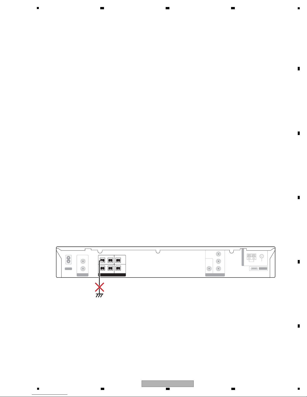
NOTES ON BTL DRIVE
As a signal to drive the BTL is output from the negative speaker terminal, DO NOT short-circuit between the negative
speaker terminal and ground, such as the chassis.
Do not short-circuit between the plus speaker terminal and ground, such as the chassis, too.
Negative Speaker Terminal
Ground (Chassis)
Do not short-circuit
6 7 8
1. SERVICE PRECAUTIONS
1.1 NOTES ON SOLDERING
A
B
1.2 CAUTION
C
D
E
5
XV-DV282AP
6 7 8
F
5
1
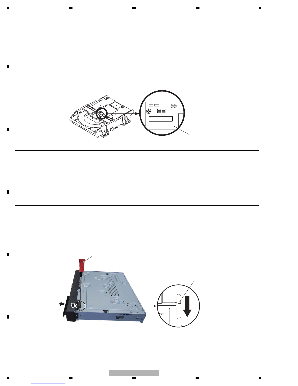
Fig. 1
Short circuit using a
soldering iron.
Pickup PCB
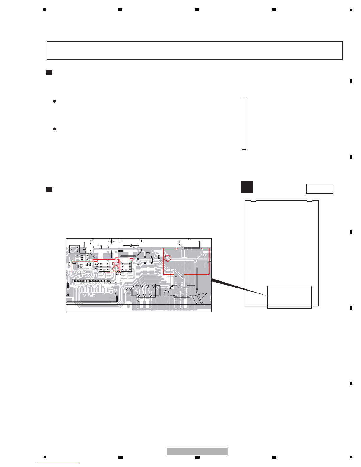
[ Removing the DVD MECHA Assy ]
Before removing Pickup PCB and DVD PCB connector, short circuit the position shown in Fig. 1 using a soldering iron.
If you remove the DVD MECHA Assy with no soldering, the Laser may be damaged.
[ Installing the DVD MECHA Assy ]
Remove all the soldering on the short circuit position after the connection of Pickup PCB and DVD PCB connector.
NOTE
• Be sure to use lead-free solder and a soldering iron.
• When Soldering/Removing of solder, use the draw in equipment over the Pickup Unit to prevent the Flux smoke from it.
How to open the tray when the power cannot be on
(1) Slide the rack, loading (White) toward the arrow direction by using a minus screwdriver to release the lock.
(2) Manually open the tray.
Note:
Please strongly pushing rack, loading (White) to release the lock because the tray doesn't go out easily.
Rack, loading (White)
Tray open
Minus screwdriver
• Bottom view
2 3 4
1.3 WHEN REPLACING DVD DECK
A
B
C
1.4 DISC REMOVAL METHOD
D
E
F
6
1
XV-DV282AP
2 3 4
5
Accessories
12 3
45 6
78 9
0
1
2
3
Power cord
(LXJ, SXJ5 : ADG1127)
Video cable
(yellow plugs)
(L = 1.5 m) (XDE3046)
FM antenna
(ADH7030)
AM loop antenna
(ATB7013)
Remote control
(
XV-DV282AP, XV-DV585K,
XV-DV590K
: XXD3185)
(
XV-DV181, XV-DV180
: XXD3186)
AA/R6 dry cell
batteries
(to confirm
system operation)
• Amplifier section
RMS Power Output:
Front, Center, Surround . . .60 W per channel
(1 kHz, 10 % T.H.D., 4 Ω)
Subwoofer. . . 60 W (100 Hz, 10 % T.H.D., 4 Ω)
• Disc section
Type. . . . . . . .DVD system, Video CD/Super VCD
system and Compact Disc digital audio system
• FM tuner section
Frequency range . . . . . . . .87.5 MHz to 108 MHz
Antenna . . . . . . . . . . . . . . . . . .75 Ω, unbalanced
• AM tuner section
Frequency range:
Saudi Arabia, Israel, South Africa, other middle
eastern contries and duty free models
. . . . . . . . . . . . . . . . . . . . . . . .531 kHz to 1602 kHz
All other models
With 9 kHz step . . . . . . . .531 kHz to 1602 kHz
With 10 kHz step . . . . . . .530 kHz to 1700 kHz
Antenna . . . . . . . . . . . . . . . . . . . . . Loop antenna
• Miscellaneous
Power requirements:
. . . . . . . . . . . .AC 220 V to 240 V, 50 Hz/60 Hz
Power consumption . . . . . . . . . . . . . . . . . . .55 W
Power consumption in standby:
For HTZ180/181DVD
. . . . . . . . . . . . . . . 0.48 W
Others
KURO LINK ON . . . . . . . . . . . . . . . . . 0.73 W
KURO LINK OFF. . . . . . . . . . . . . . . . . 0.48 W
Dimensions
. . . . . . . .420 mm (W) x 62 mm (H) x 331 mm (D)
Weight . . . . . . . . . . . . . . . . . . . . . . . . . . . . .2.8 kg
•Accessories (DVD/CD receiver)
Remote control . . . . . . . . . . . . . . . . . . . . . . . . . .1
AA/R6 dry cell batteries
(to confirm system operation) . . . . . . . . . . . . . .. 2
Video cable (yellow plugs) . . . . . . . . . . . . . . . . .1
AM loop antenna. . . . . . . . . . . . . . . . . . . . . . . . .1
FM antenna . . . . . . . . . . . . . . . . . . . . . . . . . . . . 1
Power cord . . . . . . . . . . . . . . . . . . . . . . . . . . . . .1
Setup Guide
Operating instructions
Manufactured under license from Dolby
Laboratories.
“Dolby”, “Pro Logic”, and the
double-D symbol are trademarks of Dolby
Laboratories.
Manufactured under license under U.S. Patent
#’s: 5,451,942; 5,956,674; 5,974,380; 5,978,762;
6,487,535 & other U.S. and worldwide patents
issued & pending. DTS and DTS Digital Surround
are registered trademarks and the DTS logos and
Symbol are trademarks of DTS, Inc. © 1996-2008
DTS, Inc. All Rights Reserved.
Disc/content format playback
compatibility
This player is compatible with a wide range of
disc types (media) and formats. Playable discs
will generally feature one of the following logos
on the disc and/or disc packaging. Note
however that some disc types, such as
recordable CD and DVD, may be in an
unplayable format.
See the Disc compatibility table below for more
information.
• This unit will play DVD+R/+RW discs.
• is a trademark of FUJIFILM Corporation.
• is a trademark of DVD Format/Logo
Licensing Corporation.
• Also compatible with KODAK Picture CD.
This player supports the IEC’s Super VCD
standard for superior picture quality, dual
soundtracks, and widescreen support.
DVD-Video DVD-R DVD-RW
Video CD
Fujicolor CD
CD-RWCD-RAudio CD
Super Video CD (Super VCD)
6 7 8
2. SPECIFICATIONS
2.1 SPECIFICATIONS, DISC/CONTENT FORMAT and ACCESORRIES
A
B
C
D
5
XV-DV282AP
6 7 8
E
F
7
1
Front panel
1 u STANDBY/ON
2 h OPEN/CLOSE
3 Function
4
f
5 g
6 VOLUME +/–
7 Disc tray
8 Remote Sensor
9 Display
10
USB interface
11 MIC input jacks
12 PHONES jack
MAIN
USB
SUBMIC
PHONES
h OPEN/CLOSE
u STANDBY/ON
FUNCTION
VOLUME
f g
MAIN SUBMIC
PHONES
USB
10 12
521
7
8
9
3 4
6
11
Display
1 Decord indicators
DTS lights during playback of a DTS source.
∂PLII lights during ∂Dolby Pro Logic II
decoding and ∂D lights during playback of
Dolby Digital sources.
2 PRGSVE (Except XV-DV585K, XV-DV590K)
Lights when progressive scan video signal is
given from the component video output
terminal.
3 SOUND
Lights when the SFC modes, the tone controls
(treble, bass or bass boost), MP3 Expander
mode, Voice Enhancer mode are active.
4 F.SURR.
Lights when the Extra Power mode/Front
surround mode is selected.
5 RPT and RPT-1
RPT lights during repeat play. RPT-1 lights
during repeat one-track play.
6 PGM
Lights during program or playlist playback.
7 Tuner indicators
Lights when a broadcast is being received,
Lights when a stereo FM broadcast is
being received, Lights when FM mono
reception is selected.
8 RDM
Lights during random play.
PRGSVE SOUND
DTS F.SURR.
∂
PL
∂
D
RPT -1
RECMODE
kHz
PGM
MHz RDM
6
12 89 7
5
11
3
10
21 4
9 kHz/MHz
Indicates the frequency unit shown in the
character display (kHz for AM, MHz for FM).
10 Character display
11
Lights when sleep timer is active.
12 d
Lights during playback.
XV-DV585K, XV-DV590K only
2.2 PANEL FACILITIES
A
2 3 4
B
C
D
E
F
8
1
XV-DV282AP
2 3 4
5
Remote control
The illustration shows the HTZ280/282DVD-AP.
1 u STANDBY/ON
2 Function select buttons
1
3 Number buttons, CLEAR, DISPLAY, SLEEP
and DVD controls
CLEAR
DISPLAY
SHIFT+SLEEP
SHIFT+USB REC
SHIFT+AUDIO
SHIFT+SUBTITLE
Note
1 Only the HTZ280/282DVD-AP models are equipped with the adapter port.
1
USB REC
CLEAR
TOP MENU
TUNE
ECHO
TUNE
KARAOKE
MENU
MIC VOL
PLAYLIST
OPEN/CLOSE
RETURN
SETUP
AUTO/
STEREO
MP3 EXP/
V.ENH
SURROUND
SOUND
CLASS
VOLUMECHANNEL
TV CONTROL
INPUT
SHIFT VOLUME
MUTE
T.EDIT
TESERPTESERP
AUDIO
ANGLE
SLEEP
SUBTITLE
ADAPTER PORT USB LINE
TUNER
(
FM/AM
)
DVD/CD
STANDBY
/ON
ZOOM
DISPLAY
23
456
7 8 9
0
HOME
MENU
1
2
3
ENTER
1
3
4
5
6
7
8
9
10
2
11
12
13
15
16
17
18
14
SHIFT+ANGLE
SHIFT+ZOOM
4 TOP MENU
SHIFT+SETUP
5 SHIFT+KARAOKE
SHIFT+ECHO
SHIFT+A / SHIFT+B
Cursor buttons
ENTER
TUNE
PRESET
6 HOME MENU
7 Sound controls
AUTO/STEREO
SURROUND
SOUND
MP3 EXP/V.ENH
8 Playback controls
9 TV CONTROL buttons
These control Pioneer flat screen TVs.
2
10 SHIFT
11 h OPEN/CLOSE
12 PLAYLIST buttons
13 MIC VOL +/–
14
MENU
15 RETURN
16 Tuner controls
CLASS
SHIFT+T.EDIT
17 MUTE
18 VOLUME +/–
2 Hold down the number button 1 for over three seconds with the CLEAR pressed. If the TV refuses to respond, hold down the
number button 2. After control is properly switched over, the power to the TV can be operated by directing the TVCONTROL u
toward the TV and pressing it.
6 7 8
A
B
C
D
E
F
5
XV-DV282AP
6 7 8
9
1
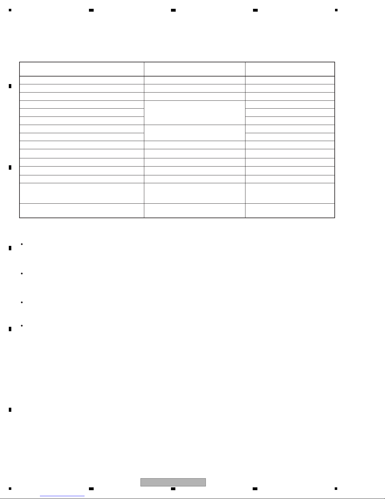
Item to be checked regarding video Item to be checked regarding audio
Block noise Distortion
Horizontal noise Noise
Dot noise Volume too low
Disturbed image (video jumpiness) Volume too high
Too dark Volume fluctuating
Too bright Sound interrupted
Mottled color
No. Procedures Check points
1
2
3
4
5
6
7
Confirm the firmware version on Test Mode. The version of the firmware must be latest.
Update firmware to the latest one, if it is not the latest.
Confirm whether the customer complain has been solved.
If the customer complain occurs with the specific disc, use it for
the operation check.
The customer complain must not be reappeared.
Video, audio and operations must be normal.
Play back a CD.
(track search)
Audio and operations must be normal.
Check the tuner (AM and FM) operations. Audio and operations must be normal.
Play back a DVD.
(Menu operation, Title/chapter search)
Video, audio and operations must be normal.
Check the sound from headphone output. Sound must be normal, without noise.
Check the appearance of the product. No scratches or dirt on its appearance after receiving it for
service.
Items to be checked after servicing / HTZ(XV)
To keep the product quality after servicing, confirm recommended check points shown below.
See the table below for the items to be checked regarding video and audio.
Cleaning
Before shipping out the product, be sure to clean the following positions by using the prescribed cleaning tools.
NamePosition to be cleaned Part No. Remarks
Cleaning liquidPickup lenses GEM1004
Cleaning paper GED-008
No. Procedures Check points
1
Confirm playback error rates at the innermost and outermost
tracks by using the following disc.
DVD test disc (GGV1025)
The error rates must be less than 5.0e-4.
(This procedure can determine if the drive is degraded.)
Specific Items to be Checked
2 3 4
3. BASIC ITEMS FOR SERVICE
3.1 CHECK POINTS AFTER SERVICING
A
B
C
D
E
F
10
1
XV-DV282AP
2 3 4
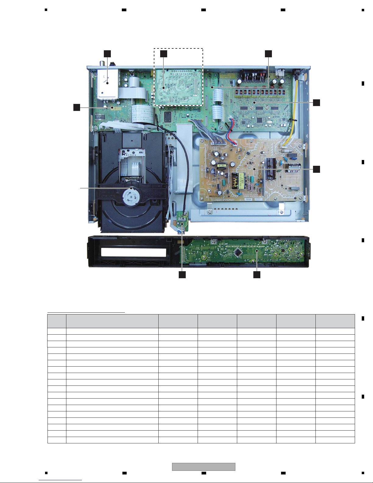
3.2 PCB LOCATIONS
NOTES: - Parts marked by “NSP” are generally unavailable because they are not in our Master Spare Parts List.
-
The > mark found on some component parts indicates the importance of the safety factor of the part.
Therefore, when replacing, be sure to use parts of identical designation.
Mark Symbol and Description
XV-DV282AP
/LXJ
XV-DV181
/LXJ
XV-DV180
/LXJ
XV-DV585K
/SXJ5
XV-DV590K
/SXJ5
1..DVD MECHA ASSY (for service) A2ZX01A650 A2ZX01A650 A2ZX01A650 A2ZX01A650 A2ZX01A650
1..09 DVDM ASSY AWM8134 AWM8134 AWM8134 AWM8134 AWM8134
1..RHTS MAIN ASSY XWM3497 XWM3520 XWM3496 XWM3505 XWM3506
2..RHTS USB ASSY XWZ4414 XWZ4414 XWZ4414 XWZ4414 XWZ4414
2..RHTS SYSMAIN ASSY XWZ4426 XWZ4454 XWZ4425 XWZ4434 XWZ4435
1..RHTS DISPLAY ASSY XWM3485 XWM3485 XWM3485 XWM3486 XWM3486
1..RHTS D-AMP ASSY XWM3490 XWM3490 XWM3490 XWM3489 XWM3489
NSP 1..NHTS JACK ASSY Not used Not used Not used AWM8034 AWM8034
2..EUROSCART ASSY Not used Not used Not used AWU8291 AWU8291
> 1..POWER SUPPLY UNIT XWR3020 XWR3020 XWR3020 XWR3020 XWR3020
1..FM/AM TUNER UNIT XXX3088 XXX3088 XXX3088 XXX3085 XXX3085
LIST OF ASSEMBLIES
FM/AM TUNER
UNIT
F
EUROSCRAT
ASSY
XV-DV585K, XV-DV590K ONLY
A
I
09 DVDM
ASSY
DVD MECHA
ASSY
H
POWER
SUPPLY
UNIT
D
RHTS D-AMP
ASSY
E
RHTS DISPLAY ASSY
C
RHTS USB ASSY
B
RHTS SYSMAIN
ASSY
5
6 7 8
A
B
C
D
5
XV-DV282AP
6 7 8
E
F
11
1
Service Remote Control Unit GGF1381
DVD Test Disc (DVD-Video) GGV1025
Adjustment, diagnosis
Name Jig No. Remarks
Check of DVD-Video
CD Test Disc STD-905 Check of CD
DVD Data Disc GGV1344 ID data setting
Jigs list
Daifree GEM1036 (ZLX-ME413A)
GYA1001 (ZLB-PN397B)
Lubricating oil
Name Lubricants and Glues No. Remarks
Refer to "9.4 DVD MECHA ASSY"
Refer to "9.4 DVD MECHA ASSY"
GEM1018Grease
Refer to "9.4 DVD MECHA ASSY"
Speaker Cable with terminal SDS1174 (FL/WHITE)
SDS1175 (FR/RED), SDS1176 (SL/BLUE)
SDS1177 (SR/GRAY), SDS6050 (C/GREEN)
For checking audio at the SP terminal
Lubricants and Glues list
2 3 4
3.3 JIGS LIST
A
B
C
D
E
F
12
1
XV-DV282AP
2 3 4

5
6 7 8
A
B
C
D
E
5
XV-DV282AP
6 7 8
F
13
1
CN2007
231
1
2
1
2
321645 97 8 10 1311 12
234
5
1
11
10
9
8
141312
7
6
15
20
21
18
19
22
23
16
17
15
13
14
12
14
12
15
13
12 534
24
523164
12 534
12 534
1
2
13246597 8 1210 11 13
4
3107
8
15131411
12
59
616
1917
18
1
1
426108 14
12
35 971113
345
2610
9871411 13
12
1816 2220 24 26
15 17 2119 23 25 27
16
15 17182122192023 252427
2631302928
283130
29
432
1
876
511
12
9
10
42 861210
13
317511
913
11
9
10
10
11
9
7
8
6
7
8
6
3
4
55
3
4
5
10
3
4
7
8
6
11
9
1
22
1
2
1
11
9
10
7
8
6
3
4
5
1
2
341
2
75
6
7614532141210 1198 1513 16 1817
CN3201
CN1
CN2
CN3101
CN966
CN965
CN964
JP1002
CN953
CN5001
JA931
CN2001
CN963
CN4009
CN4006
CN2003
CN1002
JA4003
60W
CN3
KM200NA13
B2P-VH
B3P-VH
B2P-VH
96045-17C
VKN2045-
PF13PG-C10
AKM1276-
AKM1276-
AKP7224-
96045-17C
VKN1435-
VKN1262-
IBD model
EU model
CN1
CN1
96045-15C 9604S-11C
CKS5712-A
RKN1048-
AC POWER CORD
XDX3068
XDX3087-
LIVE
NEUTRAL
NC
+B
GND
GND
+B
EV3V
SW12V
AC_DET
GND
SW5.0V
SW6.8V
SW3.3V(A)
Pwr-ctr
SW3.3V(B)
GND
FL DC-
FL DC+
-25.5V
24P FFC
GNDD
E
VCC
VREF
F
VR780
VRCOM
VR650
A
B
RF
SW
C
D
FOCS DRV
TRKG RTN
TRKG DRV
(NC) VSHF
GNDD
LD(650)
PD
LD(780)
GNDD
3.3V
RDS INT
TEST
RDS DATA
5P FFC
VKN1573-
6P FFC
VKN1574-
LOAD-
LOAD+
OPEN
GND
CLOSE
FOCS RTN
SW (GND)
LIMIT SW
SLD-
SLD+
SPD-
SPD+
V+USB
USBDM2
USBDP2
GNDUSB
GNDUSB
(XDX3068-)
5P shielded cable
V+USB
USBN
USBP
GNDD
GNDD
DATA2+
DATA2 SH
EV3V
SW12V
AC_DET
SW5.0V
GND
SW6.8V
SW3.3V(B)
Pwr-ctr
SW3.3V(A)
FL DC+
GND
FL DC-
-25.5V
HDMI OUTPUT
DATA1+
DATA2-
DATA1 SH
DATA0-
CLOCK+
DATA1-
DATA0+
DATA SH
CLOCK-
CLOCK SH
CEC
HDMISCL
NC
HOT PLUG DET
DDC/CEC GND
+5V
HDMISDA
CEC
V+5V
3R3V
3R3V
6R8V
6R8V
GNDD
GNDD
GNDD
GNDD
HPD
SCL
SDA
V+5V
GNDD
GNDD
ACK
GNDD
DOUT
V+5USB
V+5USB
DVDPOW
XDVDRST
XREADY
SCLK
SDATA
MDATA
(XDD3304)
31P FFC
CEC
SCL
V+5V
SDA
HPD
6R8V
6R8V
3R3V
3R3V
V+5V
GNDD
GNDD
GNDD
GNDD
V+5USB
V+5USB
DOUT
GNDD
SCLK
XDVDRST
XREADY
DVDPOW
GNDD
ACK
MDATA
SDATA
GNDD
VDET
MIC
XAMUTE
SUB_INT
GNDD
SY
P/XI
VSEL1
VSEL2
SQUEEZE
GNDD
GNDD
SC
ASPECT
CY/G
GNDD
VKN1248VKN1577
CN967
V
(XDD3307)
17P FFC
SUB_INT
XAMUTE
MIC
VDET
SQUEEZE
VSEL2
VSEL1
P/XI
ASPECT
SC
GNDD
V
GNDD
CY/G
GNDD
SY
GNDD
3.3V
TEST
RDS INT
RDS DATA
AM
FM
TUNED
GND
VSM
TXL
+9V
TXR
GND
CLK
DO
11P FFC
(XDD3266)
(XDD3306)
15P FFC
DI
CE
RDS
VSM
GND
TXL
TXR
+9V
GND
DO
CLK
DI
CE
GND
V+5
NC(A in L)
GND
A_OUT_R
AGND
A_OUT_L
VCC
GND
u-COM DOWNLOAD
NCNCCTRXTX
DET
TX(P_DTI)
RX(P_DTO)
GND
GND
GND
NC(A in R)
NC(RESERVE)
ID
GND
NC(SPDIF)
BLUE TOOTH
C
H
I
A 1/2,2/2
09 DVDM ASSY (AWM8134)
D
B 1/3,2/3,3/3
RHTS SYSMAIN ASSY
(XV-DV282AP/LXJ:XWZ4426)
(XV-DV181/LXJ:XWZ4454)
(XV-DV180/LXJ:XWZ4425)
(XV-DV585K/SXJ5:XWZ4434)
(XV-DV590K/SXJ5:XWZ4435)
POWER SUPPLY UNIT
(XWR3020)
FM/AM TUNER UNIT
(/LXJ:XXX3088)
(/SXJ5:XXX3085)
/SXJ5
/SXJ5
XV-DV282AP, XV-DV585K, XV-DV590K only
/LXJ
/LXJ
RHTS USB ASSY
(XWZ4414)
JCV9B07
DED012
(SW PCB)
PCB640
M
65432
1
GND(SW)
FEED MOTOR (+)
SPINDLE MOTOR (+)
SPINDLE MOTOR (-)
FEED MOTOR (-)
PICK UP INNER LIMIT SWITCH
SW2
M2601
BCZ3B03
M2602
ESE22MH24
CD2301
2H062102
M
(LOADING MOTOR PCB)
SSS-13-2
SW1
GND(SW)
SW-2(CLOSE)
SW-1(OPEN)
LOADING MOTOR(-)
LOADING MOTOR(+)
DED003
PCB610
BCZ3B52
M2603
CD2302
2H052601
M
54321
TRAVERSE MECHA ASSY
DVD MECHA ASSY (A2ZX01A650)
2 3 4
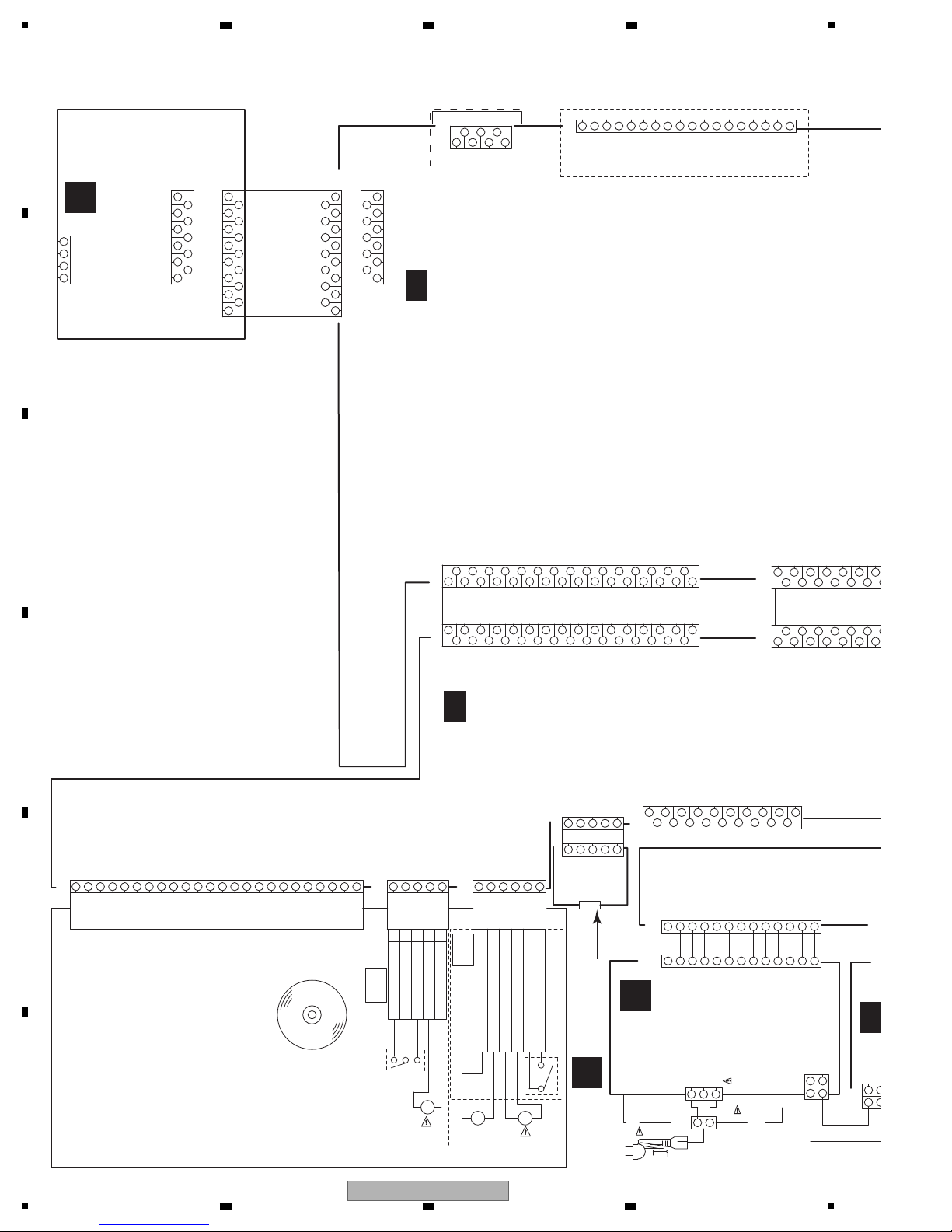
4. BLOCK DIAGRAM
4.1 OVERALL WIRING CONNECTION DIAGRAM
A
B
C
D
E
F
14
1
2 3 4
XV-DV282AP
5
Vout
GND
Vcc
1
2
1
11 810 912
2
1311 12
432
1
876
511
12
9
10
7213456
13141715
16 432
17
651098
171516131411
12
19
18
1211 13
17 1516131411
12
876
9
10
197
18
13
11
12
6
9
10
7
8
32541
16
19 171815 13
1412109811654372
1
6
13
11
9
10
7
8
12
4
1
5
3
2
432 876
51
1
12
9
10
42 861210
13
1614
14
1715
16
375119131715
3
2
1
4
5
24 8610
12
13 7591311
123
4 876510
913
12
11
14 16 2018 22
1715 19 21 23
14
17151619
2018
21 23
22
23 23
20
21
22
20
21
22
19
17
18
19
17
18
18
17
15
16
21
19
20
14
14
15
16
14
15
16
13
12
11
13
12
11
9
8
10
10
9
8
13
8
7
6
5
12
11
10
9
6
5
77
6
5
4
2
323
4
11
1
4
3
2
187
CN3201
CN2
CN3211
CN3101
CN3102
JA9100
9300
CN2001
CN2002
CN9401 CN4007
CN4005
JA4002
JA4001
CN4002 CN461
JA451
B2P-VH
AKE7121-(5.1CH)
96045-17C
XKB3062
JA3112
MIC (MAIN)
XKN3018
JA9002
96045-19C
AKN3019-
JA9001
MCACC
MIC (SUB)/
HEAD PHONE
XKN3018
GP1UE274XKC1
96045-17C
96045-19C
9607S-23F
XKB3069-
XKB3061
9604S-23C
CKS3388-
XKB3054-
AUDIO IN
XDX3087-
FL-/FR-
FL+/FR+
/XKE30611-(2.1CH)
FR-/NC
FR+/NC
C-/FL-
+B
GND
GND
+B
GND
FL DC-
FL DC+
-25.5V
XHPSEL
PCON
GNDD
3.3V
GNDD
HPR
HPL
XRST
XPDN
XMUTE
GNDD
SDA
SW-/SW-
SW+/SW+
C+/FL+
SL+/NC
SL-/NC
SR-/NC
SR+/NC
LINE_L
LINE_R
SCL
XOTW
XSD
POWER
SDATA1
SDATA3
SDATA2
GNDD
GNDD
LIN1_L
LRCLK
LIN1_R
GNDD
MCLK
GNDD
GNDD
GNDD
SCLK
S_TVOUT_L
S_TVOUT_R
GNDD
SDATA4
V+12V
RECMUTE
FL DC+
GND
FL DC-
-25.5V
(XDD3305)
17P FFC
PCON
XHPSEL
HPL
GNDD
HPR
GNDD
3.3V
SDA
GNDD
XMUTE
XPDN
XRST
HOT PLUG DET
DDC/CEC GND
+5V
GNDD
ASDAT0_ALS
13P FFC
ALRCK_CENTER
GNDD
GNDD
ABCK_ARS
ACLK_LFE
GNDD
XSD
XOTW
SCL
GNDD
POWER
SDATA3
SDATA2
SDATA1
19P FFC
(XDD3303)
GNDD
LRCLK
SCLK
MCLK
GNDD
LIN1_R
GNDD
LIN1_L
GNDD
S_TVOUT_R
S_TVOUT_L
GNDD
GNDD
V+12v
RECMUTE
SDATA4
9604S-23C
(XDD3308-)
ASDAT0_ALS
GNDD
ALRCK_CENTER
GNDD
ABCK_ARS
GNDD
ACLK_LFE
GNDD
GNDD
SY
P/XI
VSEL1
VSEL2
SQUEEZE
GNDD
GNDD
SC
ASPECT
CY/G
GNDD
CR/R
GNDD
GNDD
ASDAT2_AR
CN962
VKN1472
GNDD
GNDD
ASDAT1_AL
CB/B
GNDD
V
(XDD3307)
17P FFC
SQUEEZE
VSEL2
VSEL1
P/XI
ASPECT
SC
GNDD
V
GNDD
CY/G
GNDD
SY
CB/B
GNDD
GNDD
GNDD
CR/R
VKN1244
GNDD
ASDAT2_AR
GNDD
ASDAT1_AL
GNDD
GNDD
VE+3R3
KEY2
HP_DET
GNDD
HP_L
GNDD
HPMUTE
V+12V
KEY1
HP_R
VFDP
FLDATA
FLCS
FLDC+
MIC BIAS
MIC
GNDD
FLCK
FLDC-
GNDD
MIC_DET
23P FFC
(XDD3302-)
KEY1
KEY2
REMOCON
VE+3R3
GNDD
HPMUTE
GNDD
HP_DET
V+12V
HP_R
HP_L
GNDD
FLDC+
FLDATA
VFDP
FLDC-
MIC BIAS
MIC_DET
FLCS
FLCK
GNDD
MIC
GNDD
OUTPUT
VIDEO
COMPOSITE
Cr
OUTPUT
Y
VIDEO
COMPONENT
Cb
23P FFC (XDD3267-)
(VKB1153)
S_Y
GND
V
GND
R
S_C
DVDPOWER
S_Y
GND
V
GND
R
DVDPOWER
S_C
NC
V/Y
GND
GND
GND
GND
BLANK
R/C
GND
SCART_R
GND
B
VSEL2
V+5
SCART_L
GND
G
GND
G
GND
B
VSEL2
V+5
GND
SCART_R
SCART_L
NC
GND
L IN
GND
GND
G
NC
B
SQUEEZE
TVMUTE
GND
TVOUT_L
V+10
TVOUT_R
SQEEZE
VSEL1
TVMUTE
GND
TVOUT_L
TVOUT_R
V+10
SQEEZE
VSEL1
GND
R IN
L OUT
EURO CONNECTOR
R OUT
GND
C(S )
F
D 1/2,2/2
RHTS D-AMP ASSY
(/LXJ:XWM3490)
(/SXJ5:XWM3489)
RHTS DISPLAY ASSY
(/LXJ:XWM3485)
(/SXJ5:XWM3486)
EUROSCART ASSY
(/SXJ5:AWU8291)
/SXJ5 only
/LXJ only
E
5
6 7 8
XV-DV282AP
6 7 8
A
B
C
D
E
F
15
1
HP SEL
SYSCOM
ADMCK1
SDA
SCL
MUTE
+B
VE+3
VFDP
PCON
non DSP model : Master
DSP and DSP KARAOKE model: Slave
V+3R3
VE+3
V+12(1
V+6R8
EV 3.3V
SW 3.3V(A)
SW 12V
(10.5V)
SW 5.0V
SW 6.8V
SW 3.3V(B)
FL DC +/-
PWR
(from
RESET
PDN
SD
OTW
LRC
MC
SC
DAT
DIR
AK4117VF
ASPDIF (except NONDSP model)
ADDAT
A
24.576M
74HCU04
1.25V
OPT IN
FL
HP
FL DRIVER
KEY
REMOCON SENSOR
V+5USB
USB DP
USB DM
from DVDM
AK5358AET
TUNER
LINE
ADLRCK
ADBCK
ADDATA
12.288M
7WU04
SCART
9V
NON-DSP model only
MCACC
ADMCK0
DSP model : short
NON-DSP model : open
ALRCK
MCDATA
ACLK
MIC
ADC
ADC
AK5358AET
ALRCK
ACLK
ABCK
ASDAT1
ASDAT0
ASDAT2
ASPDIF
MCDAT
Video
AMP
BE
MT1389FE/S
27MHz
•AUDIO PROCESSING
-Audio Decode
-Bass Management
-Virtual Surround
-Preset EQ
etc.
•Build-in HDMI TRANSMITER
Y/G , Cb/B , Cr/R
Y , C
V
FTS & SPDL
DRIVER
64M
16M
64k
EEPROM
FLASH
SDRAM
Y , Cb , Cr
Y , C
V
G , B , R
SysMain
DVDMain
V+3
V+10
V+3
(KARAOKE
model only)
EEPROM
V+5V
V+6R8
SW+5
SW+V+3
SW+
V+3
V+3
VE+3
coil
VU+
V+12(10)
V+3
N
D
D
only NON-DSP
model : short
NON-DS
DSP KA
DSP mo
V+5USB
V+5USB
USB DP
USB DM
to USB Jack assy
CONT from
SYSCOM
Local +5V
SUBCOM
VE+3
SUB_SCL/
SUB_SDA
Pick up
assy
SPINDLE
MOTOR
Stepping
Motor
M
Loading
Motor
M
SUB_DATA/
SUB_CLK
MDATA/
SCLK
MD ATA/
SCLK
SDATA
SD ATA
BT(OPTION)
U-ART
V+5BT
V+5BT
MCACC
(to Audio selector)
AUDIO
selector
CEC / HOT PLUG
CEC/HOTPLUG
CONTROL between
DVD BE and SYSCOM
V+12(10)
R2114
R2131
R2130
ABCK
R2128
R2117
R2118
R2121
R2120
R4203
R4202
Main Mic Sub /MCACC
Mic
USB JACK
USB JACK
TUNER
BT ADAPTOR
(OPTION)
ORION DVD
MECHA
HDMI OUT
SW
POWER
SUPPLY
Hi-side
switch IC
Hi-side
switch IC
DISPLAY
RHTS DISPLAY ASSY
E
RHTS SYSMAIN
ASSY
B
FM/AM TUNER UNIT
I
RHTS USB ASSY
C
09 DVDM ASSY
A
POWER SUPPLY UNIT
H
IC201
IC101
IC401
IC90
IC1102
IC1103
IC601
IC802
IC9000
IC9400
IC1001
IC2201
IC2101
IC2001
IC4001
IC2103
IC2102
IC1003
2 3 4
4.2 OVERALL BLOCK DIAGRAM
A
B
C
D
E
R2129
F
16
1
XV-DV282AP
2 3 4
5
G , B , R
Y , C
V
Y, Cb, Cr
SCART
LINE
Scart
Circuit
LPF
+B
V+3R3
TAS5508B
PWM Modulator
-Volume
-Tone
-DRC
-Andrew
RESET
PWM1(FR)
SD
PWM4
HP SEL
SDA
SCL
MUTE
FL DC +/-
VFDP
PCON
V+3R3
VE+3
V+12(10)
V+6R8
PWR CONT
(from SYSCOM)
RESET
PDN
SD
OTW
DVDPOWER
(from SYSTEM U-COM)
SW
LRCLK
MCLK
SCLK
DATA0
DIR
AK4117VF
DSP
DSPC56371AF180
MCKO
LRCKO
BCKO
FDTI
FTDO
ASDAT2
ASDAT1
ADDAT
A
LCK0
BCKO
MCK0
24.576M
74HCU04
1.25V
OPT IN
ASDAT3
KEY
POWER LED
DSP model only
V+6R8
(DSP model only)
DSP
V+3
V+5V
V+3R3
P.CO
NFIG
from
DVDMAIN
V+3
NON-DSP model : open
DSP KARAOKE model : open
DSP model : short
NON-DSP model : necessary
DSP KARAOKE model : necessary
DSP model : unnecessary
NON-DSP model : short
DSP KARAOKE model : open
DSP model : open
Output Enable
from SYSCOM
IN1
IN2
OUT
SW+5
CONT/XFLAG from SUBCOM
CONT/XFLAG to SYSCOM
CONTROL
between
DSP/DIR and
SYSCOM
PWM5(L)
PWM6
(R)
PWM3
PWM2
(5.1ch model : FL
2.1ch model : FR)
PWM8(SW)
PWM7
(5.1ch model:C
2.1ch model:FL)
60W model :
TAS5122
100W model :
POWER STAGE
HP AMP
TAS5342L
(except
2.1ch model)
except 2.1ch model
FRONT R
D-AMP
MOULATOR
FRONT L
SUBWOOFER
CENTER
LINE IN
SCART
(EU, RUSSIA model only)
Component Video
(LXJ model only)
Composite
( FR for 2.1ch model)
( FL for 2.1ch model)
SURROUND R
SURROUND L
5.1ch only
V+12(10)
R2130
R2128
R2118
R2121
R4203
R4202
AC IN
DIGITAL OPT OUT
(2.1ch model only)
DIGITAL OPT IN1
(DSP model only)
Hi-side
switch IC
5V REG
Hi-side
switch IC
3.3V
PLAY
Blue : Control signal
Green : Analog Audio Signal
Black : Digital Audio Signal
Red : Voltage supply
Orange : Video Signal
Purple : Other signal
XV-DV282AP, DV181, DV585K and
DV590K are non DSP model.
Note:
RHTS D-AMP ASSY
D
EUROSCART ASSY
F
RHTS DSP ASSY
G
IC801
IC901
IC1101
IC1103
IC601
IC4501
NM
NM
IC802
IC2103
IC3201
IC3101
IC3601
IC3901
IC3301
IC3401
6 7 8
A
B
C
D
5
XV-DV282AP
6 7 8
E
F
17
1
2 3 4
4.3 DVD LOADER/DECODER BLOCK DIAGRAM
A
B
C
D
E
F
18
1
XV-DV282AP
2 3 4
5
Q305
0
Case when this diagnosis is required :
When playback of any disc, including a test disc (DVD: GGV1025, CD: STD-905), cannot be performed
How to diagnose
In the case mentioned above, degradation of the laser diodes (LDs) mounted on the Pickup PCB is suspected.
Measure the voltage between the two ends of one of the resistors mentioned below.
How to turn on the LD
Refer to “6.1 TEST MODE”.
Measure the voltage between the two ends of R322 or R325 on the 09DVDM
Assy. If the voltage is 0.4 V or higher, the 650-nm LD is degraded.
No playback of a DVD :
Measure the voltage between the two ends of R321 or R326 on the 09DVDM
Assy. If the voltage is 0.4 V or higher, the 780-nm LD is degraded.
No playback of a CD :
If the measurements show degradation
of an LD, replace the DVD MECHA
Assy.
SIDE A
A
09 DVDM ASSY
6 7 8
5. DIAGNOSIS
5.1 METHOD FOR DIAGNOSING DEGRADATION OF THE LDS ON THE PICKUP
A
B
Q304
R314
E
1
UP SIDE
C
C1
R154
1
1
D
R322
R156
Q307
L308
CONTACT
20151051
SIDE
CN101
15 15
CN102
R153
R157
R313
R152
D
C372
R305
C141
CONTACT
SIDE
R372
R371
R373
C140
CN104
R326
R375
R374
L309
Q308
C
R325
R321
D
E
5
XV-DV282AP
6 7 8
F
19
1
No. Symptoms Diagnosis Contents Possible Defective Points
1 The power is not turned on. Are wires of output connector (POWER SUPPLY Unit) and CN968 (09
DVDM Assy) disconnected or damaged ?
Connector / cable
Check that the following voltage is output :
CN968-pin 24 or pin 25 (09 DVDM Assy): 3.3 V
POWER SUPPLY Unit
2
An opening screen is not
displayed on the monitor
(The FL display lights. The
mechanism does not work.)
Are the signals output from IC201-pin 97 (MDATA) and pin 98 (SCLK)
on the 09 DVDM Assy ? (in the range of 0 to 3 V)
09 DVDM Assy
DVD IC (IC201)
Are the signals input into IC1001-pin 85 (MDATA) and pin 86 (SCLK) on
the SYSMAIN Assy ? (in the range of 0 to 3 V)
SYSMAIN Assy
UCOM (IC1001)
Check that the following voltage are output :
R1108 (V+5 V) on the SYSMAIN Assy: 5 V
POWER SUPPLY Unit /
SYSMAIN Assy R1108
Is a resonator (X201: 27 MHz) on the 09 DVDM Assy oscillating ?
09 DVDM Assy
Crystal resonator (X201)
DVD IC (IC201)
•
Is a signal input into IC203-pin26 (PCE#) on the 09 DVDM Assy ?
(Is a signal "H" for 80 ms and then "L" after the power is turned on ?)
-> Communication with flash ROM.
• Are the signals input into IC202-pin 16 (DWE#), pin 19 (DCS#)
and pin 38 (SDCLK) on the 09 DVDM Assy ?
(Is a signal fluctuating ?)
-> Communication with SDRAM
09 DVDM Assy
DVD IC (IC201)
Flash ROM (IC203)
SDRAM (IC202)
Is a signal output from IC203-pin 28 (PRD#) on the 09 DVDM Assy?
(Is a signal fluctuating for several hundred ms after the power is turned
on ?)
09 DVDM Assy
Flash ROM (IC203)
Is a signal input into IC1001-pin 11 (DVD ACK) on the SYSMAIN
Assy ? (Is a signal fluctuating ?)
-> Communication with FL Control IC
09 DVDM Assy
DVD IC (IC201)
SYSMAIN Assy
UCOM (IC1001)
Is a signal output from IC1001-pin 13 (XREADY) on the SYSMAIN Assy
? (Is a signal fluctuating in the range of 0 to 3.3 V ?)
SYSMAIN Assy
UCOM (IC1001)
Are the signals output from IC1001-pin 84 (SDATA) on the SYSMAIN
Assy ? (in the range of 0 to 3.3 V)
09 DVDM Assy
DVD IC (IC201)
SYSMAIN Assy
UCOM (IC1001)
Are the signals of IC204-pin 5 (SDA) and pin 6 (SCL) on the 09 DVDM
Assy fluctuating for one or two seconds after the power is turned?
09 DVDM Assy
EEPROM (IC204)
3
An opening screen is not
displayed on the monitor
(The FL display lights. The
mechanism works.)
Check the video signal path between DVD IC (09 DVDM Assy IC201)
and video-out terminal (see the block diagram)
09 DVDM Assy
Video circuit after DVD IC
(IC201)
Symptoms that may occur when any of the following ICs is in failure
IC Symptoms
EEP ROM
(09 DVDM Assy : IC204)
User's data cannot be stored in memory.
The ID number is lost.
Flash ROM
(09 DVDM Assy : IC203)
The power cannot be turned on.
Downloading of the firmware cannot be performed.
DVD IC
(09 DVDM Assy : IC201)
Any kind of symptoms (no power, a failure in any of the servo, video and audio systems, USB etc.) may be
generated, because the DVD processing is performed by a single chip.
64M SDRAM
(09 DVDM Assy : IC202)
No power.
Block noise is generated during playback.
2 3 4
5.2 DVD TROUBLE SHOOTING
A
B
C
D
E
F
20
1
XV-DV282AP
2 3 4
5
No. Symptoms Diagnosis Contents Possible Defective Points
4 A tray cannot be opened.
(An opening screen is
displayed on the monitor)
Does the voltage of CN965-pin 1 and pin 2 on the 09 DVDM Assy
change normally ?
Pin 1 (CLOSE (TRIN)): Tray is fully closed: "L"
Pin 3 (OPEN (TROUT)): Tray is fully opened: "L"
DVD MECHA Assy
Switch (SW1)
Is the signal input into IC101-pin 1 (TROPEN) on the 09 DVDM Assy?
At open: 3.3 V, At close: 0 V
09 DVDM Assy
DVD IC (IC201)
Are the signals output from CN965-pin 5 and pin 4 on the 09 DVDM Assy ?
Pin 5: Approx. 5 V during opening tray approx. 1 V during closing tray.
Pin 4: Approx. 0 V during opening tray approx. 6 V during closing tray.
09 DVDM Assy
FTS Driver IC (IC101)
Are wires of CN964 and CN965 on the 09 DVDM Assy disconnected or
damaged ?
Connector / cable
Does the voltage of CN964-pin 5 on the 09 DVDM Assy change to 0 V
by pressing the Push switch.
Push switch (SW2)
5 Playback impossible
(no focusing)
Are the signals output from IC101-pin 16 (F+) and pin 15 (F–) on the 09
DVDM Assy ?
09 DVDM Assy
FTS Driver IC (IC101)
Does 650-nm LD emit light ?
Does a pickup lens move up / down ?
Does an actuator spring bend ?
Pickup
Are plastic parts damaged ? Or is a shaft detached ?
Is the turntable detached or tilted ?
Mechanism section (motor)
Is flexible cable of CN965 on the 09 DVDM Assy disconnected or
damaged ?
Flexible cable / connector
Is signal output from IC201-pin 41 (FOSO) on the 09 DVDM Assy ?
(Device control of about 1.4 V is output usually. It is fluctuated by about
250 mV with focus up / down.)
09 DVDM Assy
DVD IC (IC201)
6 Playback impossible
(Spindle does not turn)
Are the signals output from IC101-pin 12 (MOT_SPDL–) and pin 11
(MOT_SPDL+) on the 09 DVDM Assy ?
Is pin 21 (STBY) fixed LOW ? (pin 21 is High at playback: 3 V)
09 DVDM Assy
FTS Driver IC (IC101)
Is there any part detached from the spindle motor ?
Or Is there any foreign object lodged in it ?
Mechanism section
(Spindle motor)
Are wires of CN964 on the 09 DVDM Assy disconnected or damaged ?
Flexible cable / connector
Is signal output from IC201-pin 36 (DMSO) on the 09 DVDM Assy ?
09 DVDM Assy
DVD IC (IC201)
7 Playback impossible
(Playback stops)
Does 650-nm LD deteriorate ?
If the voltage at each both ends of R322 and R325 on the 09 DVDM
Assy is 0.4 V or more, the 650-nm LD is definitely deteriorated.
650-nm LD deteriorated.
(When pla
yback of a DVD is
impossible)
Does 780-nm LD deteriorate ?
If the voltage at each both ends of R321 and R326 on the 09 DVDM
Assy is 0.4 V or more, the 780-nm LD is definitely deteriorated.
780-nm LD deteriorated.
(When playback of a CD is
impossible)
Are there scratches or dirt on the disc ? Disc
8 Picture disturbance during
playback
(block noise, freeze, other)
Are there scratches or dirt on the disc ?
Is there a problem with the format of the disc ?
Check the video signals.
Composite video signal (IC401-pin 23)
S video signal (IC401-pin 21, pin 26)
RGB video signal (IC401-pin 16, pin 18, pin 20)
Disc
9 No sound
(Picture is normal)
Check the waveform (ALCK: IC201-pin 231), (ALRCK: IC201-pin 227),
(ABCK : IC201-pin 230), (ASDATA0/1/2: IC201-pin 226/225/223).
Check the waveform (ASPDIF: IC201-pin 215)
09 DVDM Assy
DVD IC (IC201)
09 DVDM Assy
DVD IC (IC201)
Video IC (IC401)
6 7 8
A
B
C
D
E
5
XV-DV282AP
6 7 8
F
21
1
Filter
and
Volume
Timing
Control
Gate
Drive
XSD
To UCOM
PCM Signal
From
DVD or ADC
3.3 V
0 V
TAS5508BPAG
PWM Processor section
PWM Processor section
Power Stage section
Power Stage section
Output LPF section
Output LPF section
TAS5122DCA
XOTW
Protection
PCM -> PWM
Gate
Drive
20 V
0 V
0 V
0 V
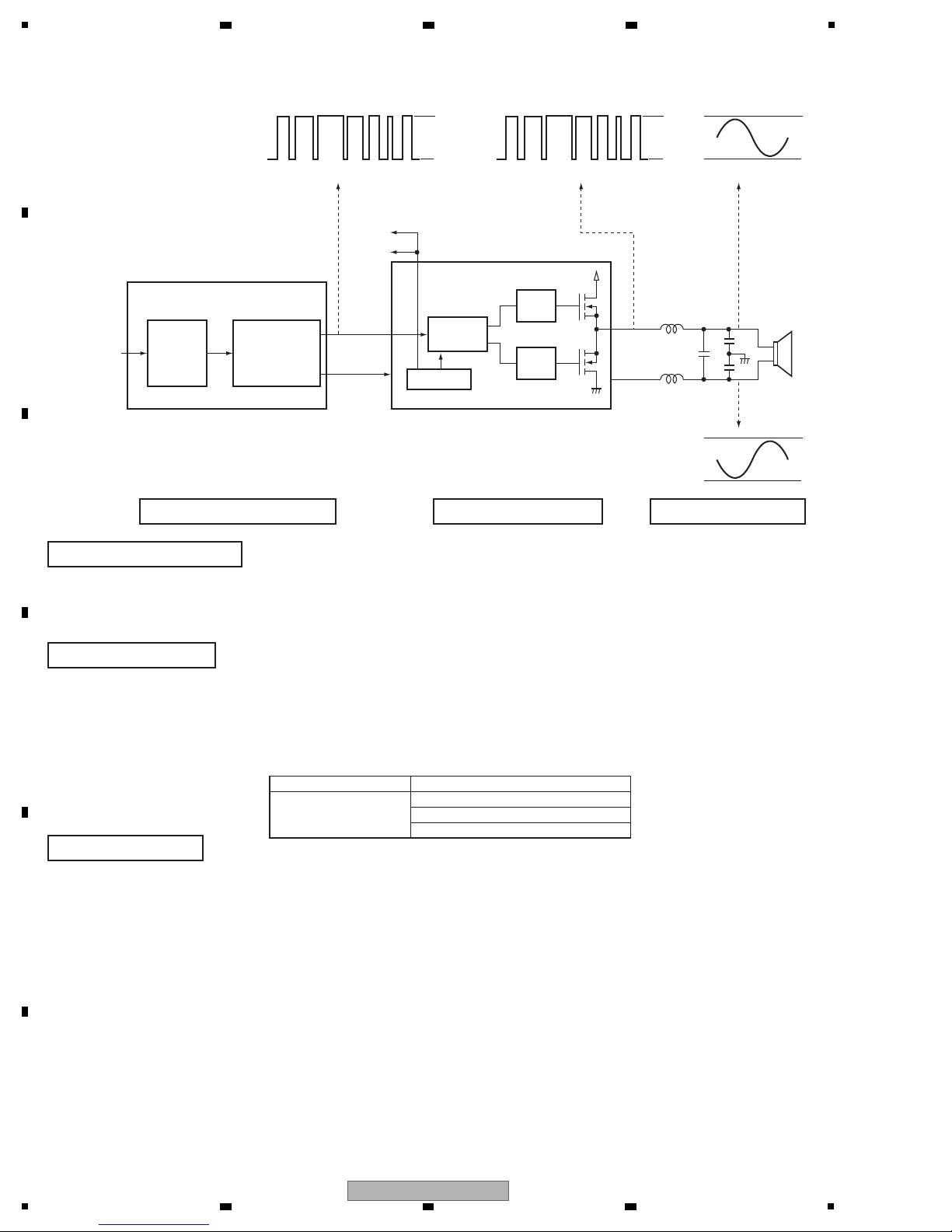
The PCM signals output from the DVD decoder or AD converter are input to this section, and their volume and sound quality
are digitally adjusted. At the output stage, after conversion from PCM to PWM, the signals are output to the Power stage.
In this section, timing is controlled so that the MOSFETs on the high and low sides will not be turned on simultaneously. The
voltage of the PWM signals are raised to drive the gates of the MOSFET, and the PWM signals to drive the speakers are
output from the MOSFET at the output stage. Detection and protection functions against short-circuiting of the output
signals and temperature exceeding the standard value are also provided.
The carrier elements, high-frequency signals that are unnecessary for these speakers, are eliminated. The signals passed
through the LPF will become sine-wave signals, as shown in the figure above.
Power Stage ICs No. Protection Enable State
IC3201 SD_AB (pin 23) => L
IC3301 SD_CD (pin 24) => L
IC3401 OTW (pin 25) => L
IC3101 IC3201, IC3301, IC3401
*1 XSD : SD_AB (pin 23), SD_CD (pin 24)
*2 XOTW : OTW (pin 25)
*1
*2
If the detection and protection work, the ports of the power stage ICs become the following state.
2 3 4
5.3 CIRCUIT DESCRIPTION OF DIGITAL AMP SECTION
A
B
C
D
E
F
22
1
XV-DV282AP
2 3 4

5
The protection circuits for the Digital Amplifier are activated, following the specifications shown below. The error indication on
the FL display shows the reason a protection circuit was activated.
Upon diagnosis of the Digital Amplifier, refer to the specifications for the protection circuits here and the overview of the Digital
Amplifier circuitry.
1. Overview
The system microcomputer monitors the ports for shutdown requests (pin 23: SD_AB and pin 24: SD_CD) and the ports for
abnormal-temperature detection (pin 25: /OTW) of the Power Stage ICs (IC3201, IC3301, and IC3401). As soon as any
abnormality is detected, it shuts the unit down.
To notify the user of the possibility of a too high a volume, when the unit is turned on the next time, the volume level will be set
to 0, and an error message will be displayed on the FL display.
2. Ports on the system microcomputer to be used for detection
Pin 71: SHUTDOWN
Low voltage at this pin means overcurrent or voltage too low (= V+B27) at a Power Stage IC.
Pin 78: XOTW
Low voltage at this pin means the temperature at the Power Stage ICs exceeded 125 °C.
Note: As one Power Stage IC is provided with two channels, three Power Stage ICs (in total 6 channels) are mounted in
this unit. For abnormality detection, the unit implements a logical OR operation regarding these three ICs.
Therefore, which IC is abnormal cannot be known directly. To find which IC is abnormal, it is required to check the
PWM outputs (pins 35, 38, 47, 50) of the each power stage ICs (IC3201, IC3301, IC3401).
3. Detection timing
Start : Detection starts 500 ms after the PWRCONT port (pin 34) of the system microcomputer becomes active by your
pressing the STANDBY/ON key.
Finish : When the STANDBY/ON key is pressed again (when the power-off process starts).
4. Operation of the protection circuits
The following three protection circuits are activated when the conditions shown below are met:
Overcurrent detection 1: Indication on the FL display: OC ERR 1
Conditions: If the SHUTDOWN ports, which are monitored every 10 ms, become low 7 times in succession
Overcurrent detection 2: Indication on the FL display: OC ERR 2
Conditions: The PCONFIG ports (pin 58), which are monitored every 30 ms, become more than 2 Vrms more than 45 %
in one minute.
Abnormal temperature detection 1: Indication on the FL display: OVERTEMP
Conditions: If the XOTW ports, which are monitored every 10 ms, become low in succession for one minute.
Abnormal temperature detection 2: Indication on the FL display: OVERTEMP
(Prerequisite: The XOTW ports, which are monitored every 10 ms, become low three times in succession.)
Conditions: The above prerequisite is upheld, and the conditions for an overcurrent detection are met.
5. Process when the protection circuits are activated
The unit is shut down within 30 ms after abnormality detection then the volume level is set to 0.
The unit can be turned on immediately after the shutdown.
6 7 8
5.4 SPECIFICATIONS FOR THE PROTECTION CIRCUITS FOR THE DIGITAL
AMPLIFIER
A
B
C
D
E
XV-DV282AP
5
6 7 8
F
23
1
USB related warning
USB over current detect error (over 500 mA)
HDCP authentication failed after HDMI cable was connected.
If the set has no HDCP key, it causes this error.
HDMI related warning
Power consumption by Bluetooth ADAPTER is too high to supply the power.
Reconnect the Bluetooth ADAPTER.
Source change to BT from source other than BT.
When cannot detect a device at BT function
BT ADAPTER related warning
SBUERR
DM IHERR
TBERR
TBAUDIO
ODN E V ICE
↓
ADAPTER PORT terminal sequence in BT AUDIO function
H
ADP_DE T
L
H
V P+5
L
H
ADP_DT I
indefinite
L
H
ADP_DT O
L
About 1.5 second
DATA
DATA
DATA
ADAPT ER POR T
ADP_ DE T logic
ADP_DE T
In non-connectionHIn connection
L
2 3 4
5.5 ERROR AND WARNING MESSAGE
A
B
C
D
E
F
24
1
XV-DV282AP
2 3 4
5
Step 1: Connect AS-BT100 (Bluetooth adapter)
Step 2: Playback check
JA4003
To Step 2
Yes
No
No
Yes
No
Yes
Yes
No
Yes
No
Yes
No
Function switch ⇒ FL display
Are the AS-BT100
(Bluetooth adapter) securely
inserted?
Insert the adapter securely.
Check the P_PORT_DET,
P_PORT_ID.
Check the path. V+5BT
Are the ANALOG
signals output?
JA4003 16, 14PIN
JA4003 17PIN
Is the voltage 5 V ?
(V+5BT input)
Check the P_PORT_DTI, P_PORT_DTO.
Refer to the service manual (AS-BT100).
Check the Step 1.
Refer to the service manual (AS-BT100).
Check the IC1102 5 PIN
Check IC1101 and the power supply circuits
when the voltage of IC1102 1PIN is not 5 V.
The over current protection is operating
when ’BT ERR’ is indicated on FL display.
Check the power supply circuits
or AS-BT100 is abnormal status.
(Refer to the service manual (AS-BT100).)
Does the BT AUDIO
function appear?
Is
'NODEVICE' displayed?
(BT AUDIO indication does not
continue it.), Be done
the pairing?
Refer to the block diagram
and the circuit diagram,
and confirm the signal path.
Note: Outside factors such as setting of the Bluetooth device,
affinity and radio waves environment may be causes.
5.6 ADAPTER PORT TROUBLESHOOTING
6 7 8
A
B
C
D
5
XV-DV282AP
6 7 8
E
F
25
1
POWER ON SEQUENCE for RegularHTS. (KURO LINK OFF)
Items Signal name on SYSCOM start end
SMPS ON PWRCONT (34pin) 20 6000
Start AC DET Monitoring ACDET (81pin) 20 6000
Start XPROTECT Monitoring XPROTECT (54pin) 1520 6000
DVD Power DVDPOWER (15pin) 450 6000
Cancel DVD Reset XDVDRST (14pin) 600 6000
Start DVD Communication
SDATA /MDATA /SCLK
(84,85,86pin)
1000 6000
Start VDET Monitoring VDET (53pin) 1520 6000
SUB u-com Power ON SUBPOWER (17pin) 20 6000
Cancel SUB u-com Reset SUB_RESET (16pin) 300 6000
Start SUB Communication
SDATA /MDATA /SCLK
(84,85,86pin)
1000 6000
Start FL Control
XFLCS / FLDATA / FLCLK
(38, 39, 40pin)
400 6000
Start TUNER Communication
TXIDATA /TXCLK /TXODATA /TXCE
(3, 5, 6, 19pin)
300 6000
RDS POW ON RDS POW (9pin) 20 6000
Cancel DIR Reset XDIRRST (68pin) 960 6000
Cancel DSP Reset XDSPRST (64pin) 1160 6000
Cancel TAS Reset XDARST (76pin) 3360 6000
Start DAMP initialization
DASCK,DASDA
(1, 2pin)
3560 6000
Start HPDET/MICDETMonitoring
HPDET /MIC DET
(49,60pin)
3760 6000
Start SHUTDOWN Monitoring XSHUTDWN (71pin) 1260 6000
Start PCONFIG Monitoring PCONFIG (58pin) 3560 6000
Start Over Temp Monitoring XOTW (78pin) 1260 6000
Key Mask - 0 2080
SYS Mute ON DMUTECHECK (22pin) 0 2080
AMP Mute ON DSPMUTE (70pin)
0 5860
Power Step
20 20 360 120 1300 120 120 20
STEP0^1 STEP1^2 STEP2^3 STEP3^4 STEP4^5 STEP5^6 STEP6^7 STEP7^8
40 400 520 1820 1940 2060 2080
0 200 400 600 800 1000 1200 1400 1600 1800 2000 2200 2400 2600 2800
SMPS ON
Start AC DET Monitoring
Start XPROTECT Monitoring
DVD Power
Cancel DVD Reset
Start DVD Communication
Start VDET Monitoring
SUB u-com Power ON
Cancel SUB u-com Reset
Start SUB Communication
Start FL Control
Start TUNER Communication
RDS POW ON
Cancel DIR Reset
Cancel DSP Reset
Cancel TAS Reset
Start DAMP initialization
Start HPDET/MICDETMonitoring
Start SHUTDOWN Monitoring
Start PCONFIG Monitoring
Start Over Temp Monitoring
Key Mask
SYS Mute ON
AMP Mute ON
Power Step
this process is performed only
when last function is DVD/CD.
Power ON
(User operation is
admitted)
* I specify the shortest case in power on co
STANDBY/ON key
is pressed.
2 3 4
5.7 POWER ON SEQUENCE
A
B
C
D
E
F
26
1
XV-DV282AP
2 3 4
5
20
2600 2800 3000 3200 3400 3600 3800 4000 4200 4400 4600 4800 5000 5200 5400 5600 5800 6000
sound is output
6 7 8
A
B
C
D
E
5
XV-DV282AP
6 7 8
F
27

1
Test Mode Functional Specification
1 Test mode entry
In the power ON state, press the [ESC] key and [TEST] key in order of the Test mode remote control unit.
• OSD displays test mode.
2 LD ON
Enter the test mode.
DVD : Press the [TEST] and [1] keys in order, and turn on the laser diode (650 nm).
CD : Press the [TEST] and [4] keys in order, and turn on the laser diode (780 nm).
3 Release the Test mode
• Turn off the power.
• Press the [ESC] key of the remote control unit and reset it.
2 3 4
6. SERVICE MODE
6.1 TEST MODE
A
B
C
D
E
F
28
1
XV-DV282AP
2 3 4
5
Character in bold : Item name
: Information display
1
5
6
10
11
8
9
3
2
12
15
13
14
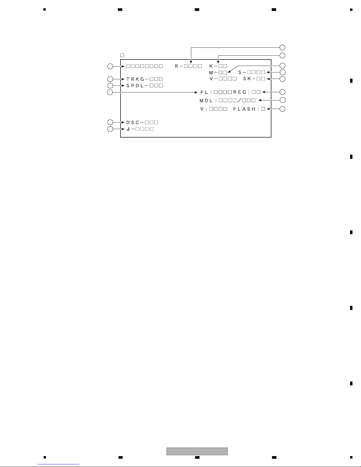
1 Address indication
The address being traced is displayed in number.
(as for the DVD, indication of decimal number is possible.)
DVD : ID indication (hexadecimal number, 8 digits)
[* * * * * * * *]
CD : ID indication [* * * * * * * *]
2 Code indication of remote control unit [R – * * * *]
In case of double code, display a 2nd code.
3 Main unit keycode indication [K – * *]
5 Tracking status [TRKG – * * *]
Tracking on : [ON]
Tracking off : [OFF]
6 Spindle status [SPDL – * * *]
CLV : [CLV]
Off : [OFF]
7 Mechanism (loading) position value [M – * *]
Unknown : [01] or [41]
Open state : [04]
Close state : [08]
During opening : [12]
During closing : [22]
8 Slider position [S – * * * *]
In Side Switch ON : [01]
In Side Switch OFF : [00]
9 Output video system [V – * * * *]
NTSC system : [NTSC]
PAL system : [PAL]
Automatic setting : [AUTO]
Scart terminal output [SK – * *]
(Display only the WY model which can do the output
setting of scart terminal.)
VIDEO : [00]
S-VIDEO : [01]
RGB : [02]
a Disc sensing [DSC – * * *]
The type of discs loaded is displayed.
[DVD], [CD ]
b Jitter value [J – * * * *]
Note: Don't use it.
c Version of the FL controller [FL: * * * *]
Note: Don't use it.
d Region setting of the player [REG: *]
Setting value : [1] to [6]
e Destination setting of the FL controller
[MDL: * * * * / * * *]
Four characters in the front represent code 01.
Three characters in the back represent the destination
code.
f Version of the flash ROM [V: * *. * *]
Flash ROM size [FLASH = * *]
7
J: Japan, K: North America, R: General Area,
LB: Taiwan, WY: Europe, TH: Thai, RAM: China
6 7 8
6.2 DISPLAY SPECIFICATION OF THE TEST MODE
A
B
C
D
E
5
XV-DV282AP
6 7 8
F
29
1
Service mode indication (ESC + CHP/TIM keys)
ID Address
The error rate is always displayed in exponential notation, e.g., *.* * e - *, for both DVDs and CDs.
EDC/ID/AV 1 error history (ID Address, EDC/ID Error, last eight errors)
Calculation of the average error rate (ESC + "5" [Test mode remote control unit] keys)
The average of the last eight error rates is calculated and indicated in exponential notation. After the calculation is completed, "OK" or "NG" is
displayed. If "NG" is displayed, the disc tray will open (for both DVDs and CDs)
For DVDs: OK with 5.0e-4 or less, for CDs: OK with 7.6e-3 or less
Indication of model information (ESC + CHAP keys)
For details, see 6.4.
Region confirmation mode (ESC + A.MON [Test mode remote control unit] + "1"-"6" [Test mode remote control unit] keys)
After you press the A.MON key while holding the ESC key pressed and then input the region number, if the number is different from that set in
the unit, an error message is displayed, and the tray opens.
Command Contents Conditions
Remote Control Key Name
Memory clear and region / revision indication CLEAR (*1)
Average value measurement of DVD error rate 5 (*1)
CD error rate measurement 5 (*1)
Scart terminal output : VIDEO
Models equipped with Scart terminal
AUDIO
Scart terminal output : S-VIDEO SUBTITLE
Scart terminal output : RGB ANGLE
Progressive OFF
Only for progressive models
Only for HDMI models
R_SKIP
Progressive ON F_SKIP
FL indication of ID number STEREO (*1)
ZOOM ON (x4) ZOOM
Service mode indication (error rate indication, etc.) CHP/TIM (*1)
Model information indication CHAP (*1)
Title search Input mode IN
Title No. input
Search execution
SIDE A (*1)
Numbers (*1)
PLAY (*1)
Region confimation mode
A.MON (*1)
Numbers (*1)
Only during normal playback, the following shortcut keys can be assigned by pressing a required key after pressing the ESC
key of the remote control unit. To quit, press the ESC key
*1 : Test mode remote control unit
HDMI Resolution : 1920 x 1080p PROGRAM
2 3 4
6.3 FUNCTIONAL SPECIFICATION OF THE SHORTCUT KEY
A
B
C
D
E
F
30
1
2 3 4
XV-DV282AP
 Loading...