

Page 1
2010
VSX-1020-K
For details, refer to "Important Check Points for good servicing".
AUDIO/VIDEO MULTI-CHANNEL RECEIVER
VSX-1020-K
VSX-1025-K
THIS MANUAL IS APPLICABLE TO THE FOLLOWING MODEL(S) AND TYPE(S).
Model Type Power Requirement Remarks
VSX-1020-K UXCNCB AC 120 V
VSX-1025-K CUXCN AC 120 V
ORDER NO.
RRV4045
PIONEER CORPORATION 1-1, Shin-ogura, Saiwai-ku, Kawasaki-shi, Kanagawa 212-0031, Japan
PIONEER ELECTRONICS (USA) INC. P.O. Box 1760, Long Beach, CA 90801-1760, U.S.A.
PIONEER EUROPE NV Haven 1087, Keetberglaan 1, 9120 Melsele, Belgium
PIONEER ELECTRONICS ASIACENTRE PTE. LTD. 253 Alexandra Road, #04-01, Singapore 159936
PIONEER CORPORATION
K-IZK MAR.
2010 Printed in Japan
Page 2
1
1. SAFETY PRECAUTIONS
The following check should be performed for the
continued protection of the customer and service
technician.
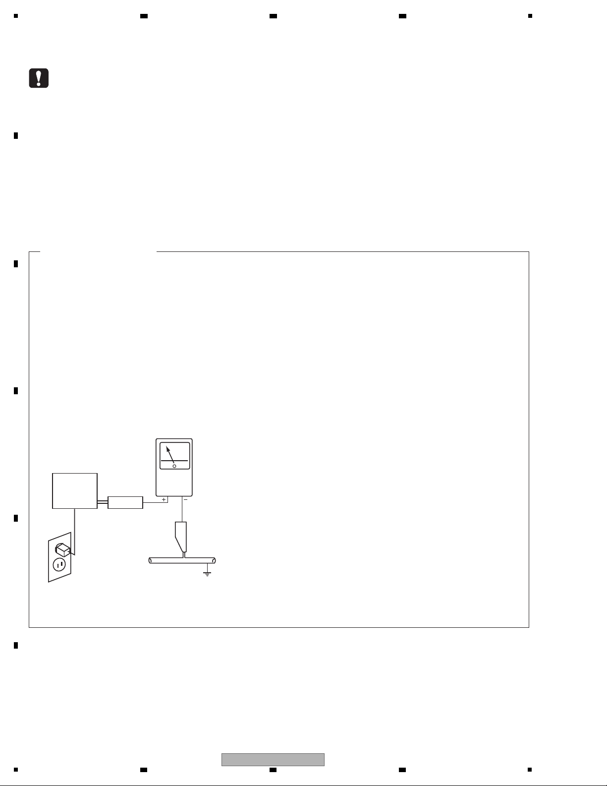
LEAKAGE CURRENT CHECK
Measure leakage current to a known earth ground
(water pipe, conduit, etc.) by connecting a leakage
current tester such as Simpson Model 229-2 or
equivalent between the earth ground and all exposed
metal parts of the appliance (input/output terminals,
screwheads, metal overlays, control shaft, etc.). Plug
the AC line cord of the appliance directly into a 120V
AC 60 Hz outlet and turn the AC power switch on. Any
current measured must not exceed 0.5 mA.
ANY MEASUREMENTS NOT WITHIN THE LIMITS
OUTLINED ABOVE ARE INDICATIVE OF A POTENTIAL
SHOCK HAZARD AND MUST BE CORRECTED BEFORE
RETURNING THE APPLIANCE TO THE CUSTOMER.
2. PRODUCT SAFETY NOTICE
Many electrical and mechanical parts in the appliance
have special safety related characteristics. These are
often not evident from visual inspection nor the protection
afforded by them necessarily can be obtained by using
replacement components rated for voltage, wattage, etc.
Replacement parts which have these special safety
characteristics are identified in this Service Manual.
Electrical components having such features are
identified by marking with a > on the schematics and on
the parts list in this Service Manual.
The use of a substitute replacement component which
does not have the same safety characteristics as the
PIONEER recommended replacement one, shown in the
parts list in this Service Manual, may create shock, fire,
or other hazards.
Product Safety is continuously under review and new
instructions are issued from time to time. For the latest
information, always consult the current PIONEER Service
Manual. A subscription to, or additional copies of,
PIONEER Service Manual may be obtained at a nominal
charge from PIONEER.
Leakage
current
tester
Reading should
not be above
0.5 mA
Device
under
test
Test all
exposed metal
surfaces
Also test with
plug reversed
(Using AC adapter
plug as required)
Earth
ground
AC Leakage Test
(FOR USA MODEL ONLY)
WARNING
This product may contain a chemical known to the State of California to cause cancer, or birth defects or other reproductive
harm.
Health & Safety Code Section 25249.6 - Proposition 65
This service manual is intended for qualified service technicians ; it is not meant for the casual do-ityourselfer. Qualified technicians have the necessary test equipment and tools, and have been trained
to properly and safely repair complex products such as those covered by this manual.
Improperly performed repairs can adversely affect the safety and reliability of the product and may
void the warranty. If you are not qualified to perform the repair of this product properly and safely, you
should not risk trying to do so and refer the repair to a qualified service technician.
2 3 4
SAFETY INFORMATION
A
B
C
D
E
F
2
1
2 3 4
VSX-1020-K
Page 3
5
[Important Check Points for Good Servicing]
In this manual, procedures that must be performed during repairs are marked with the below symbol.
Please be sure to confirm and follow these procedures.
1. Product safety
Please conform to product regulations (such as safety and radiation regulations), and maintain a safe servicing environment by
following the safety instructions described in this manual.
1 Use specified parts for repair.
Use genuine parts. Be sure to use important parts for safety.
2 Do not perform modifications without proper instructions.
Please follow the specified safety methods when modification(addition/change of parts) is required due to interferences such as
radio/TV interference and foreign noise.
3 Make sure the soldering of repaired locations is properly performed.
When you solder while repairing, please be sure that there are no cold solder and other debris.
Soldering should be finished with the proper quantity. (Refer to the example)
4 Make sure the screws are tightly fastened.
Please be sure that all screws are fastened, and that there are no loose screws.
5 Make sure each connectors are correctly inserted.
Please be sure that all connectors are inserted, and that there are no imperfect insertion.
6 Make sure the wiring cables are set to their original state.
Please replace the wiring and cables to the original state after repairs.
In addition, be sure that there are no pinched wires, etc.
7 Make sure screws and soldering scraps do not remain inside the product.
Please check that neither solder debris nor screws remain inside the product.
8 There should be no semi-broken wires, scratches, melting, etc. on the coating of the power cord.
Damaged power cords may lead to fire accidents, so please be sure that there are no damages.
If you find a damaged power cord, please exchange it with a suitable one.
9 There should be no spark traces or similar marks on the power plug.
When spark traces or similar marks are found on the power supply plug, please check the connection and advise on secure
connections and suitable usage. Please exchange the power cord if necessary.
a Safe environment should be secured during servicing.
When you perform repairs, please pay attention to static electricity, furniture, household articles, etc. in order to prevent injuries.
Please pay attention to your surroundings and repair safely.
2. Adjustments
To keep the original performance of the products, optimum adjustments and confirmation of characteristics within specification.
Adjustments should be performed in accordance with the procedures/instructions described in this manual.
4. Cleaning
For parts that require cleaning, such as optical pickups, tape deck heads, lenses and mirrors used in projection monitors, proper
cleaning should be performed to restore their performances.
3. Lubricants, Glues, and Replacement parts
Use grease and adhesives that are equal to the specified substance.
Make sure the proper amount is applied.
5. Shipping mode and Shipping screws
To protect products from damages or failures during transit, the shipping mode should be set or the shipping screws should be
installed before shipment. Please be sure to follow this method especially if it is specified in this manual.
6 7 8
A
B
C
D
5
VSX-1020-K
6 7 8
E
F
3
Page 4

1
2 3 4
CONTENTS
SAFETY INFORMATION ..........................................................................................................................................................2
1. SERVICE PRECAUTIONS ....................................................................................................................................................5
A
B
C
D
E
F
1.1 NOTES ON SOLDERING ...............................................................................................................................................5
1.2 NOTES ON REPLACING PARTS ...................................................................................................................................5
1.3 CAUTION ........................................................................................................................................................................5
2. SPECIFICATIONS .................................................................................................................................................................6
2.1 SPECIFICATIONS...........................................................................................................................................................6
2.2 PANEL FACILITIES .........................................................................................................................................................7
3. BASIC ITEMS FOR SERVICE.............................................................................................................................................11
3.1 CHECK POINTS AFTER SERVICING..........................................................................................................................11
3.2 PCB LOCATIONS .........................................................................................................................................................12
3.3 JIGS LIST......................................................................................................................................................................13
4. BLOCK DIAGRAM...............................................................................................................................................................14
4.1 OVERALL WIRING DIAGRAM......................................................................................................................................14
4.2 DIGITAL AUDIO BLOCK DIAGRAM..............................................................................................................................16
4.3 ANALOG AUDIO BLOCK DIAGRAM ............................................................................................................................18
4.4 DIGITAL VIDEO BLOCK DIAGRAM..............................................................................................................................19
4.5 ANALOG VIDEO BLOCK DIAGRAM ............................................................................................................................20
4.6 GND BLOCK DIAGRAM ...............................................................................................................................................22
5. DIAGNOSIS.........................................................................................................................................................................25
5.1 DIAGNOSIS FLOWCHART...........................................................................................................................................25
5.2 ERROR INDICATIONS..................................................................................................................................................40
6. SERVICE MODE .................................................................................................................................................................41
6.1 TEST MODE .................................................................................................................................................................41
7. DISASSEMBLY ....................................................................................................................................................................43
8. EACH SETTING AND ADJUSTMENT ................................................................................................................................50
8.1 HOW TO UPDATE FIRMWARE ....................................................................................................................................50
8.2 IDLE CURRENT ADJUSTMENT ..................................................................................................................................53
9. EXPLODED VIEWS AND P
ARTS LIST...............................................................................................................................54
9.1 PACKING SECTION......................................................................................................................................................54
9.2 EXTERIOR SECTION...................................................................................................................................................56
10. SCHEMATIC DIAGRAM ....................................................................................................................................................60
10.1 AUDIO ASSY ..............................................................................................................................................................60
10.2 COMPONENT ASSY ..................................................................................................................................................62
10.3 COMPOSITE, MIC, F-VIDEO and BRIDGE2 ASSYS.................................................................................................64
10.4 F-HDMI, USB MTG and HDMI MTG ASSYS ..............................................................................................................66
10.5 AMP ASSY..................................................................................................................................................................68
10.6 DISPLAY, HEADPHONE and POWER SW ASSYS....................................................................................................70
10.7 D-MAIN ASSY (1/12) ..................................................................................................................................................72
10.8 D-MAIN ASSY (2/12) ..................................................................................................................................................78
10.9 D-MAIN ASSY (3/12) ..................................................................................................................................................80
10.10 D-MAIN ASSY (4/12) ................................................................................................................................................82
10.11 D-MAIN ASSY
(5/12) ................................................................................................................................................84
10.12 D-MAIN ASSY (6/12) ................................................................................................................................................86
10.13 D-MAIN ASSY (7/12) ................................................................................................................................................88
10.14 D-MAIN ASSY (8/12) ................................................................................................................................................90
10.15 D-MAIN ASSY (9/12) ................................................................................................................................................92
10.16 D-MAIN ASSY (10/12) ..............................................................................................................................................94
10.17 D-MAIN ASSY (11/12) ..............................................................................................................................................96
10.18 D-MAIN ASSY (12/12) ..............................................................................................................................................98
10.19 MAIN and BRIDGE1 ASSYS ..................................................................................................................................100
11. PCB CONNECTION DIAGRAM ......................................................................................................................................102
11.1 AUDIO ASSY ............................................................................................................................................................102
11.2 COMPONENT ASSY
................................................................................................................................................104
11.3 COMPOSITE, MIC, F-VIDEO and BRIDGE2 ASSYS...............................................................................................106
11.4 F-HDMI, USB MTG and HDMI MTG ASSYS ............................................................................................................108
11.5 AMP ASSY................................................................................................................................................................110
11.6 DISPLAY, HEADPHONE and POWER SW ASSYS..................................................................................................114
11.7 D-MAIN ASSY...........................................................................................................................................................118
11.8 MAIN ASSY...............................................................................................................................................................122
11.9 BRIDGE1, GUIDE3 GIUIDE-L and GUIDE-R ASSYS ..............................................................................................126
12. PCB PARTS LIST ............................................................................................................................................................128
4
1
2 3 4
VSX-1020-K
Page 5
5
• For environmental protection, lead-free solder is used on the printed circuit boards mounted in this unit.
Be sure to use lead-free solder and a soldering iron that can meet specifications for use with lead-free solders for repairs
accompanied by reworking of soldering.
• Compared with conventional eutectic solders, lead-free solders have higher melting points, by approximately 40 ºC.
Therefore, for lead-free soldering, the tip temperature of a soldering iron must be set to around 373 ºC in general, although
the temperature depends on the heat capacity of the PC board on which reworking is required and the weight of the tip of
the soldering iron.
Do NOT use a soldering iron whose tip temperature cannot be controlled.
Compared with eutectic solders, lead-free solders have higher bond strengths but slower wetting times and higher melting
temperatures (hard to melt/easy to harden).
The following lead-free solders are available as service parts:
• Parts numbers of lead-free solder:
GYP1006 1.0 in dia.
GYP1007 0.6 in dia.
GYP1008 0.3 in dia.
The part listed below is difficult to replace as a discrete component part.
When the part listed in the table is defective, replace whole Assy.
EMMA2RL2 UPD61283F1-407LU2A BGA
IC1501 HDMI Receiver SII9233ACTU IC with heat-pad
Assy Name
D-MAIN Assy
IC800
7028069261010-IL
PCB Assy Part No.
Ref No. Function Part No.
Parts that is Difficult to Replace
Remarks
• Discharging
For more detail, please refer to “7. DISASSEMBLY - 1. Discharging”.
• Notes on Ground Points Connection
For more detail, please refer to “7. DISASSEMBLY - 2. Notes on Ground Points Connection”.
6 7 8
1. SERVICE PRECAUTIONS
1.1 NOTES ON SOLDERING
A
B
1.2 NOTES ON REPLACING PARTS
1.3 CAUTION
C
D
E
F
VSX-1020-K
5
6 7 8
5
Page 6
1
iPod cable
(L308102013010-IL)
Accessories
Remote control
(8300759500010-IL)
AM loop antenna
(ATB7013)
FM wire antenna
(ADH7030)
Dry cell batteries
(AAA size IEC R03) x2
Microphone (for Auto MCACC setup)
(APM7008)
(VSX-1020-K)
(VSX-1025-K)
2. SPECIFICATIONS
2.1 SPECIFICATIONS
A
B
2 3 4
C
D
E
F
6
1
2 3 4
VSX-1020-K
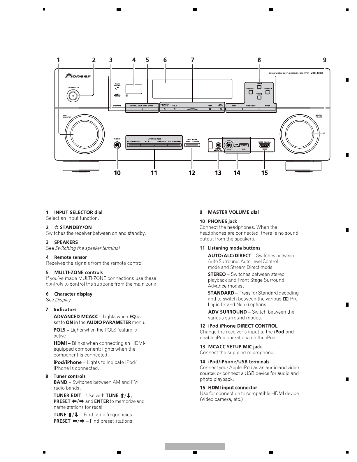
Page 7
Front panel
5
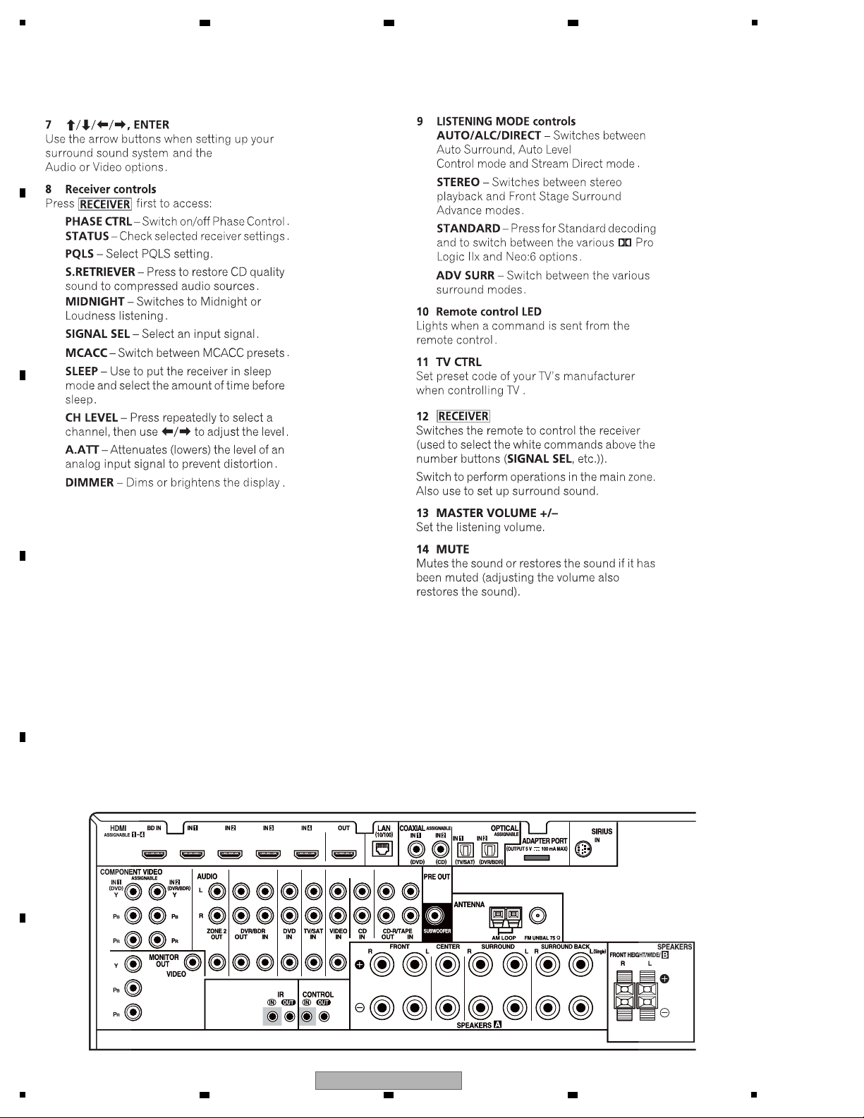
2.2 PANEL FACILITIES
6 7 8
A
B
C
D
E
F
VSX-1020-K
5
6 7 8
7
Page 8
A
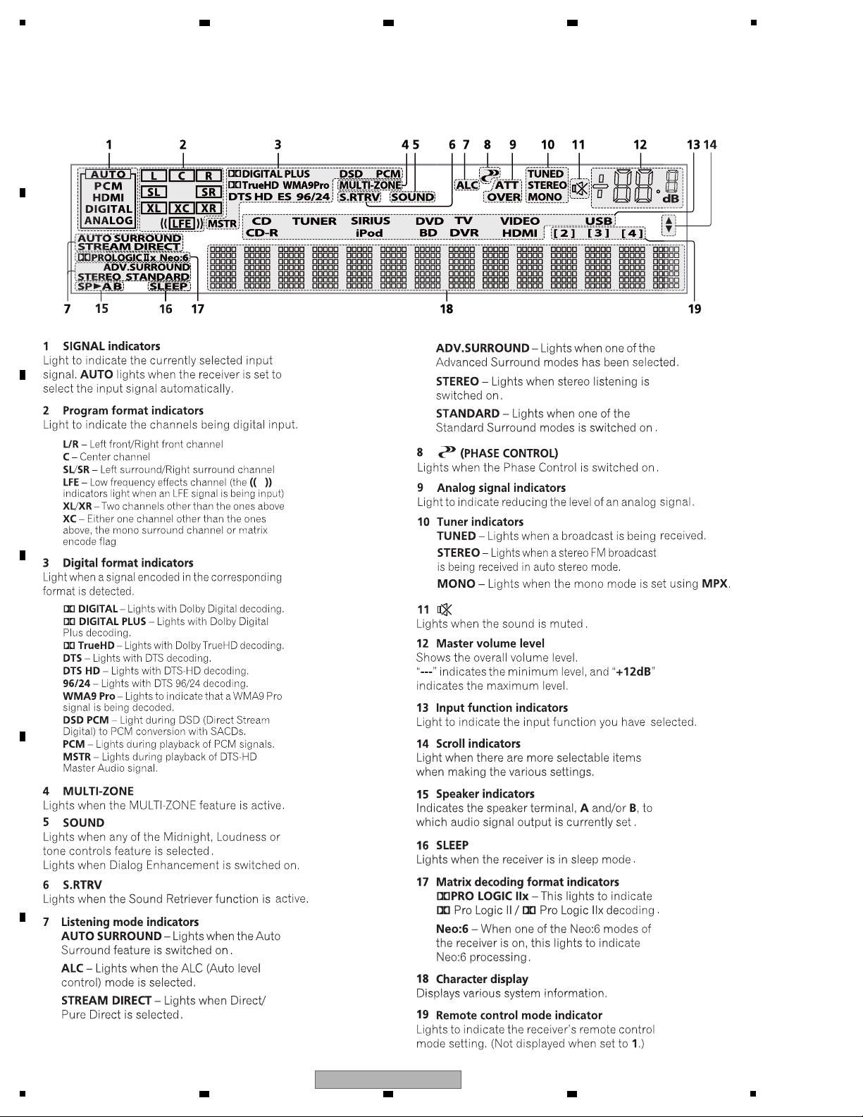
Display
B
1
2 3 4
C
D
E
F
8
1
2 3 4
VSX-1020-K
Page 9
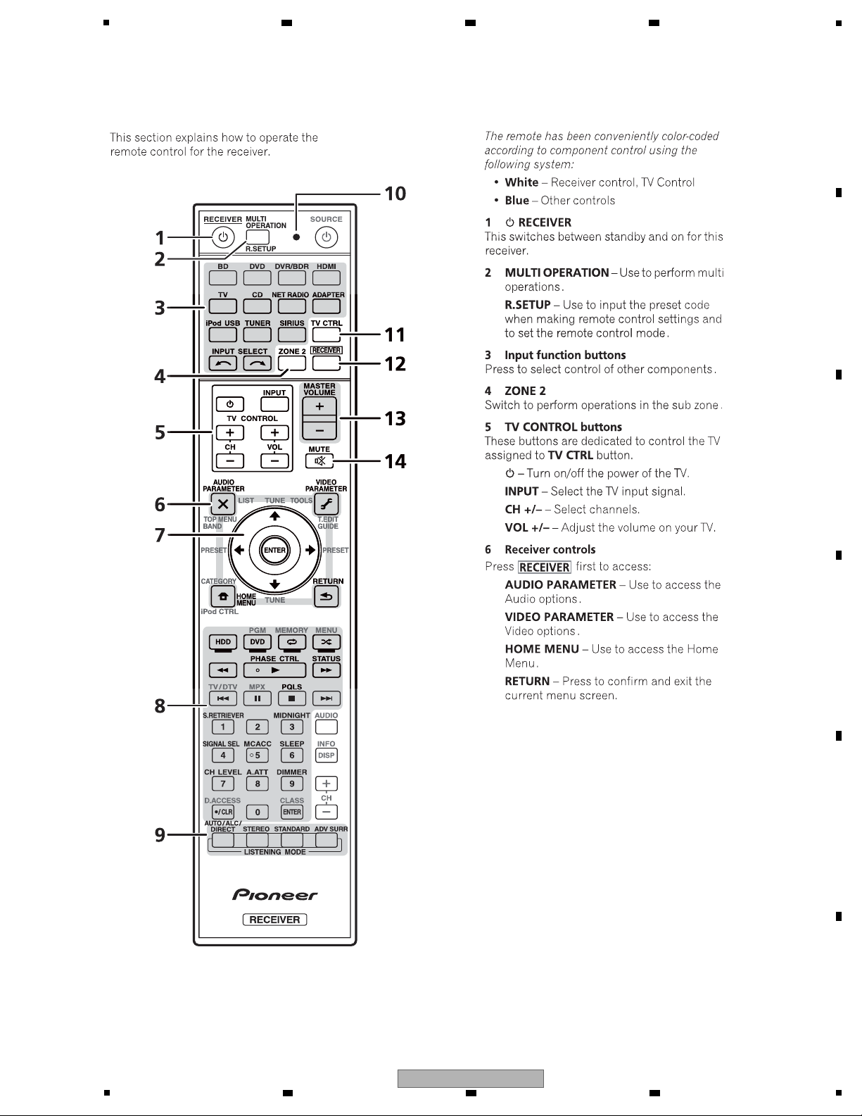
Remote control
5
6 7 8
A
B
C
D
E
F
VSX-1020-K
5
6 7 8
9
Page 10
1
Rear panel
A
B
2 3 4
C
D
E
F
10
1
2 3 4
VSX-1020-K
Page 11
5
Item to be checked regarding video Item to be checked regarding audio
Block noise Distortion
Horizontal noise Noise
Flicker Volume too low
Disturbed image (video jumpiness) Volume too high
Too dark Volume fluctuating
Too bright Sound interrupted
Mottled color
No. Procedures Check points
1
2
3
4
5
6
7
8
Confirm whether the customer complain has been solved.
If the customer complain occurs with the particular source,
such as Dolby Digital, DTS, AAC, DVD-A and HDMI, input it for
the operation check.
The customer complain must not be reappeared.
Video, Audio and operations must be normal.
Check the analog audio playback.
(Make the analog connections with a DVD player.)
Each channel audio and operations must be normal.
Check the digital audio playback.
(Make the digital connections with a DVD player.)
Each channel audio and operations must be normal.
Check surround playback.
(Select Surround mode and check the multichannel operations
via the DSP circuit.)
Each channel audio and operations must be normal.
Check the tuner (AM and FM) operations. Audio and operations must be normal.
Check the video outputs.
(Connect with a DVD player.)
Video and operations must be normal.
Check the sound from headphone output. Sound must be normal, without noise.
Check the appearance of the product. No scratches or dirt on its appearance after receiving it for
service.
Items to be checked after servicing / VSX, SC
To keep the product quality after servicing, confirm recommended check points shown below.
See the table below for the items to be checked regarding video and audio.
6 7 8
3. BASIC ITEMS FOR SERVICE
3.1 CHECK POINTS AFTER SERVICING
A
B
C
D
E
F
VSX-1020-K
5
6 7 8
11
Page 12
1
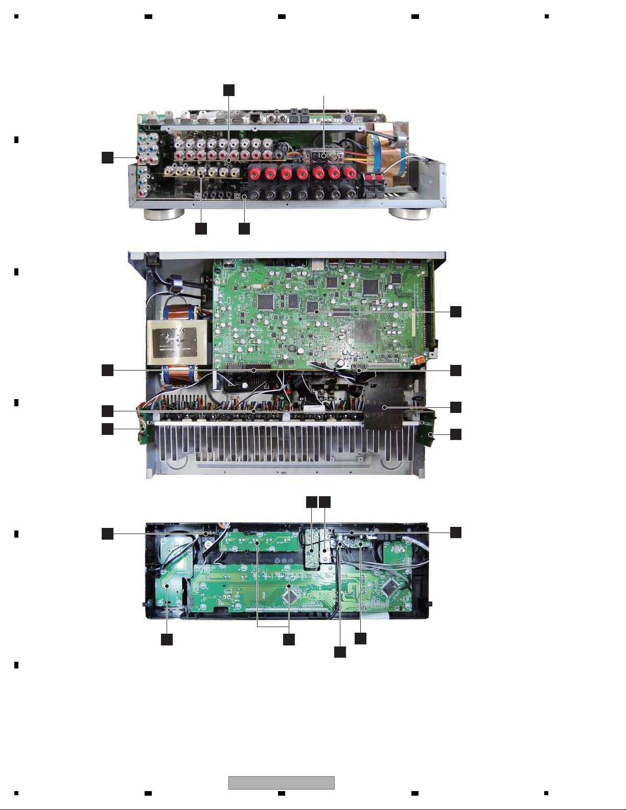
MAIN ASSY
O
DISPLAY ASSY
K
USB MTG ASSY
H
HDMI MTG ASSY
I
POWER SW ASSY
M
COMPOSITE ASSY
C
N
D-MAIN ASSY
P
BRIDGE1 ASSY
G
F-HDMI ASSY
Q
GUIDE3 ASSY
S
GUIDE-R ASSY
B
COMPONENT
ASSY
J
AMP ASSY
F
BRIDGE2 ASSY
L
HEADPHONE
ASSY
R
GUIDE-L ASSY
AUDIO ASSY
A
MIC ASSY F-VIDEO ASSY
D E
FM/AM TUNER UNIT
3.2 PCB LOCATIONS
A
2 3 4
B
C
D
E
F
12
VSX-1020-K
1
2 3 4
Page 13
5
NSP 1..MAIN ASSY 7025HK0918010-IL
2..MAIN ASSY 7028069211010-IL
2..BRIDGE1 ASSY 7028069213010-IL
2..GUIDE-L ASSY 7028069214010-IL
2..GUIDE-R ASSY 7028069215010-IL
2..GUIDE3 ASSY 7028069218010-IL
NSP 1..FRONT ASSY (VSX-1020-K) 7025HK0918011-IL
NSP 1..FRONT ASSY (VSX-1025-K) 7025HK0918051-IL
2..DISPLAY ASSY (VSX-1020-K) 7028069221010-IL
2..DISPLAY ASSY (VSX-1025-K) 70280692210C0-IL
2..POWER SW ASSY 7028069222010-IL
2..USB MTG ASSY 7028069223010-IL
2..HDMI MTG ASSY 7028069224010-IL
2..HEADPHONE ASSY 7028069225010-IL
NSP 1..AMP ASSY 7025HK0918012-IL
2..AMP ASSY 7028069531010-IL
NSP 1..INPUT ASSY 7025HK0918013-IL
2..AUDIO ASSY 7028069241010-IL
2..COMPONENT ASSY 7028069242010-IL
2..COMPOSITE ASSY 7028069243010-IL
2..BRIDGE2 ASSY 7028069244010-IL
2..F-VIDEO ASSY 7028069245010-IL
2..MIC ASSY 7028069246010-IL
NSP 1..F-HDMI ASSY 7025HK0918014-IL
2..F-HDMI ASSY 7028069251010-IL
NSP 1..D-MAIN ASSY 7025HK0918015-IL
2..D-MAIN ASSY 7028069261010-IL
Mark No. Description Part No. Mark No. Description Part No.
LIST OF ASSEMBLIES
NOTES: - Parts marked by “NSP” are generally unavailable because they are not in our Master Spare Parts List.
-
The > mark found on some component parts indicates the importance of the safety factor of the part.
Therefore, when replacing, be sure to use parts of identical designation.
Jigs List
Jig Name Part No. Remarks
7P extension jig cable GGD1671 Diagnosis (AMP Assy ↔ MAIN Assy)
2P short connector jig GGD1672 Diagnosis (Posistor ↔ MAIN Assy)
13P extension jig cable GGD1669 Diagnosis (AMP Assy ↔ AUDIO Assy)
8P extension jig cable GGD1670 Diagnosis (AMP Assy ↔ MAIN Assy)
Board to board extension jig cable GGD1675 Diagnosis (COMPONENT Assy ↔ MAIN Assy)
Lubricants and Glues List
Name Part No. Remarks
Silicon grease GEM1057 Refer to “9.2 EXTERIOR SECTION”.
Silicon adhesive GYA1011 (KE40RTV-W) Refer to “9.2 EXTERIOR SECTION”.
6 7 8
A
B
3.3 JIGS LIST
C
D
E
VSX-1020-K
5
6 7 8
F
13
Page 14
1
J
AMP
(702
O
MAIN ASSY
(7028069211010-
K
DISPLAY ASSY
(7028069221010-IL: VSX-1020-K)
(70280692210C0-IL: VSX-1025-K)
G
F-HD
(702
L
HEADPHONE ASSY
(7028069225010-IL)
Q
GUIDE3 ASSY
(7028069218010-IL)
M
POWER SW ASSY
(7028069222010-IL)
H
USB MTG ASSY
(7028069223010-IL)
I
H
(
POWER TRANS
FM/AM
TUNER UNIT
R
GUIDE-L ASSY
(7028069214010-IL)
S
GUIDE-R ASSY
(7028069215010-IL)
-
When ordering service parts, be sure to refer to "EXPLODED VIEWS and PARTS LIST" or "PCB PARTS LIST".
-
The > mark found on some component parts indicates the importance of the safety factor of the part.
Therefore, when replacing, be sure to use parts of identical designation.
-
: The power supply is shown with the marked box.
2 3 4
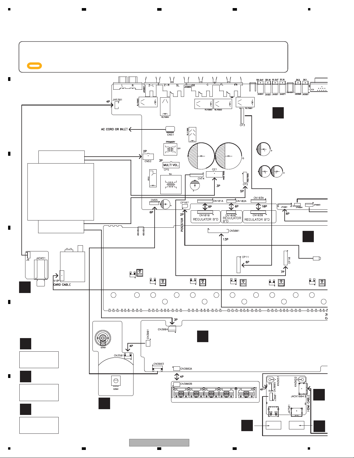
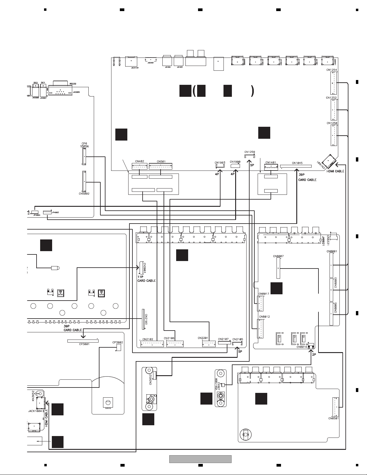
4. BLOCK DIAGRAM
4.1 OVERALL WIRING DIAGRAM
A
B
C
D
E
F
14
1
2 3 4
VSX-1020-K
Page 15
5
A
AUDIO ASSY
(7028069241010-IL)
J
AMP ASSY
(7028069531010-IL)
ASSY
B
COMPONENT ASSY
(7028069242010-IL)
D
MIC ASSY
(7028069246010-IL)
F
BRIDGE2 ASSY
(7028069244010-IL)
P
BRIDGE1 ASSY
(7028069213010-IL)
G
F-HDMI ASSY
(7028069251010-IL)
I
HDMI MTG ASSY
(7028069224010-IL)
E
F-VIDEO ASSY
(7028069245010-IL)
C
COMPOSITE ASSY
(7028069243010-IL)
CN7612
CN7601
CN7602
CN7614
CN7615CN7613
D-MAIN ASSY
(7028069261010-IL)
N
N N
1/12- 12/12
A
B
C
A
B
C
6 7 8
A
B
C
D
5
6 7 8
VSX-1020-K
E
F
15
Page 16
1
N
D-MAIN ASSY
2 3 4
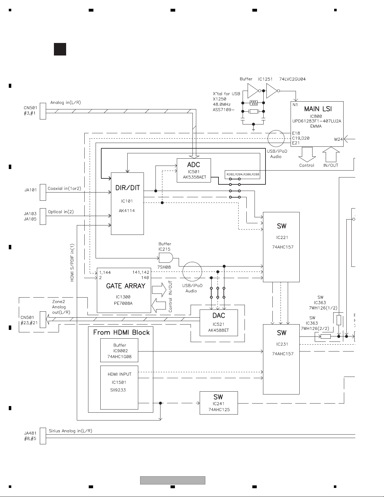
4.2 DIGITAL AUDIO BLOCK DIAGRAM
A
B
C
D
E
F
16
1
2 3 4
VSX-1020-K
Page 17
5
6 7 8
A
B
C
D
E
F
VSX-1020-K
5
6 7 8
17
Page 18
1
A
AUDIO ASSY
DIGITAL AUDIO BLOCK
Selector / Volume / PRE Amp
IC2501
BD3473KS2
2 3 4
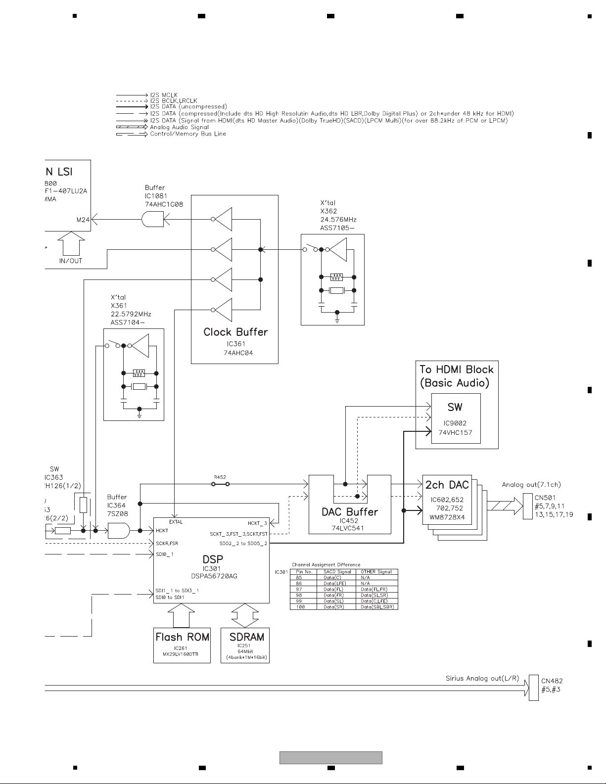
4.3 ANALOG AUDIO BLOCK DIAGRAM
A
B
C
D
E
F
18
1
2 3 4
VSX-1020-K
Page 19
5
N
D-MAIN ASSY
6 7 8
4.4 DIGITAL VIDEO BLOCK DIAGRAM
A
B
C
D
E
F
VSX-1020-K
5
6 7 8
19
Page 20
1
B
COMPONENT ASSY
E
F-VIDE
2 3 4
4.5 ANALOG VIDEO BLOCK DIAGRAM
A
B
C
D
E
F
20
1
2 3 4
VSX-1020-K
Page 21
5
C
COMPOSITE ASSY
E
F-VIDEO ASSY
6 7 8
A
B
C
D
E
F
VSX-1020-K
5
6 7 8
21
Page 22
1
N
D-MAIN ASSY
D
MIC ASSY
E
F-VIDEO
ASSY
B
COMPONENT ASSY
C
COMPOSITE ASSY
A
AUDIO ASSY
G
F-H
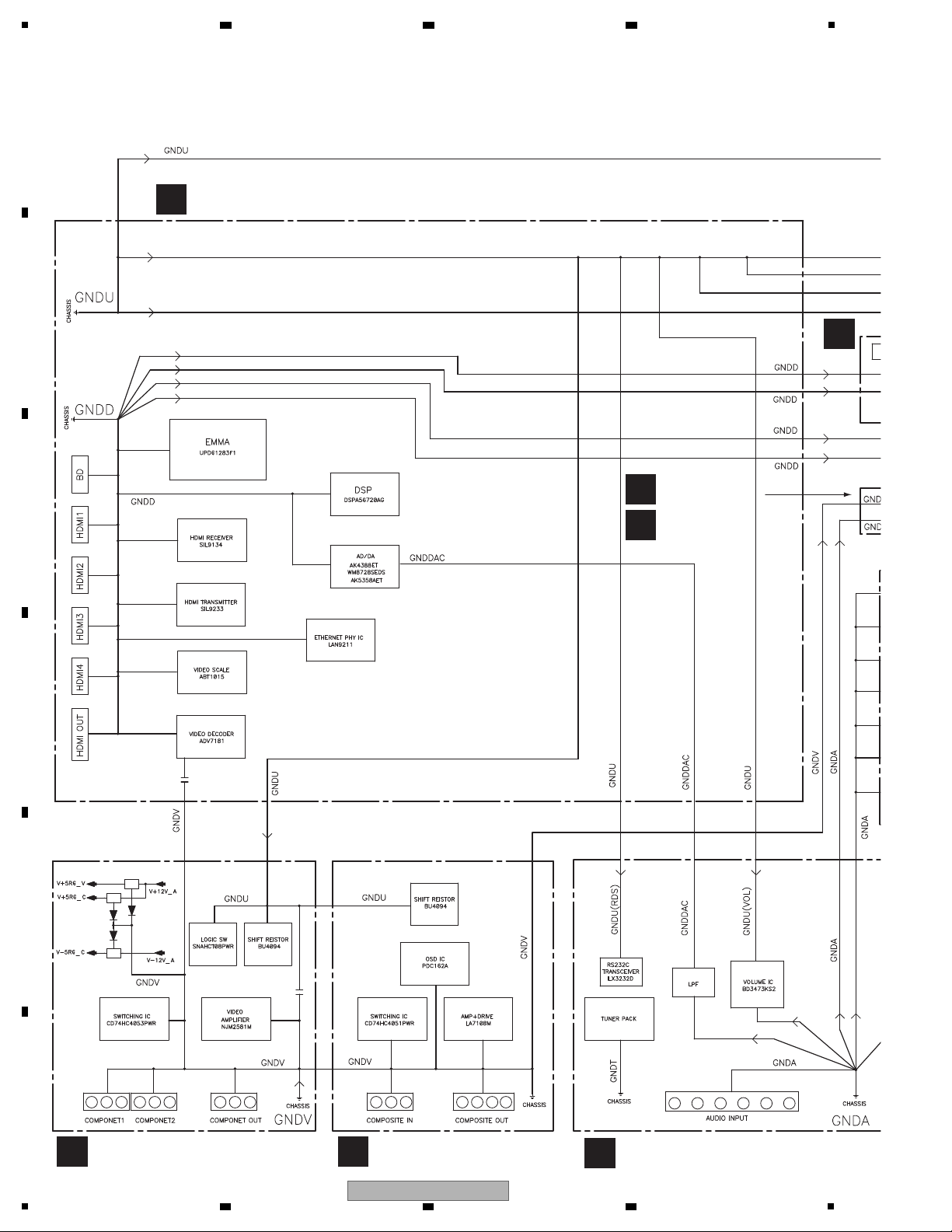
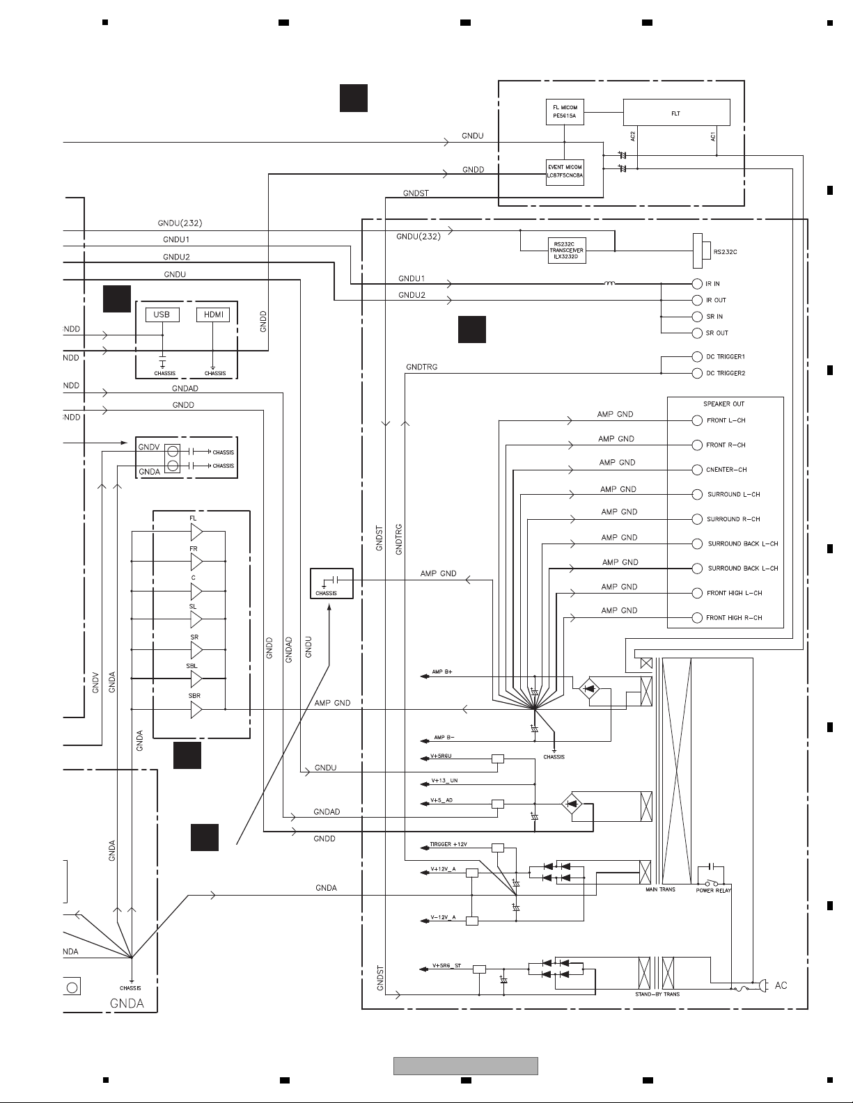
4.6 GND BLOCK DIAGRAM
A
B
2 3 4
C
D
E
F
22
1
VSX-1020-K
2 3 4
Page 23
O
MAIN ASSY
J
AMP ASSY
L
HEADPHONE ASSY
G
F-HDMI ASSY
K
DISPLAY ASSY
5
6 7 8
A
B
C
D
E
5
VSX-1020-K
6 7 8
F
23
Page 24

1
A
B
2 3 4
C
D
E
F
24
1
2 3 4
VSX-1020-K
Page 25
5
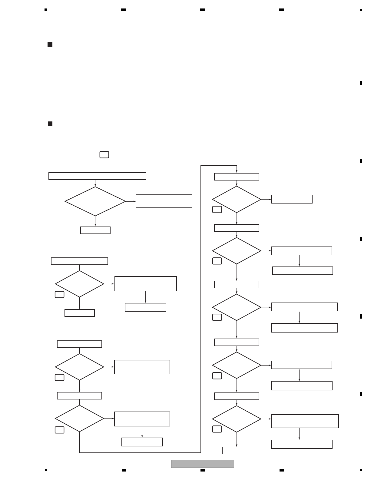
Step 1: MUTE pin
Replace IC301.
Replace D582.
To Step 2
To Step 3
Step 0: Preliminary confirmation
Confirm the following items before checking
Do
screws of
earth terminal (KN481)
securely tighten
?
Tighten screws securely.
Note:
If this section is not fixed,
the GND for DSP module
may lifted from the chassis
and cause instable potential
and lead to product failures.
No
Ye s
To Step 1
IC301 (Pin 84) (or R324)
Is the
voltage of output
signal 0 V
?
No
No
Ye s
Replace IC582 (side B).
NG
Replace IC581.
NG
DSP1MUTE
V+5_DDD1
Check the Q1900 and
its periphery block.
Check the C121, C114,
C509 and C459.
Check the C333.
IC581 (Pin 1)
Is the
voltage of around
5 V input?
Is the
voltage of 3.3 V
output?
No
Ye s
(to chassis)
V+3R3_D
(to chassis)
D582 (Cathode)
Is the
voltage of around
2.7 V output
?
No
Ye s
IC581 (Pin 3)
No
Ye s
Is the
voltage of 1 V
input?
C333 (+ side)
No
Ye s
V+1_DSPF
NG
Check the C506 and C527.
Check the MAIN Assy.
Is the
voltage of 5 V
input?
C506 (+ side)
No
Ye s
V+5_DAC
NG
Check the C606, C656, C706
and C756.
Replace Q551 (side B).
Is the
voltage of 5 V
input?
C606 (+ side)
No
Ye s
V+5_DACA
NG
Check the C552.
Replace R552.
Is the
voltage of around
5 V input?
C552 (+ side)
No
Ye s
V+5_DACD
Step 2: Power supply
Simplified diagnosis
Errors in the Audio Part of the D-MAIN Assy (those simply and roughly predictable by machine operation only)
• Sound abnormality in Delay
If sound abnormality does not occur in the Delay OFF state but occurs in the Delay ON state, it is most likely that a failure
has occurred in SDRAM (IC251) or LATCH (IC281, IC291) in the DSP Part.
• No sound at analog signal input
If sound abnormality does not occur with digital signal input (COAX, OPT, etc.) but occurs only with analog signal input,
it is most likely that a failure has occurred in the AD converter (IC501).
• No sound with the PQLS ON (normal sound with the PQLS OFF)
If no sound is output during CD playback with the PQLS ON, it is most likely that a failure has occurred in the crystal
oscillator (X361). (Diagnosis point A)
<If no sound is output in Multi-Channel-Signal Playback or Surround mode with the COAX, OPT, USB, and HDMI inputs>
• Assume that the LCRs are neither in poor connection nor damaged.
• Assume that diagnosis is performed from Side A.
• This shows failure analysis for the DSP Part of the D-MAIN Assy.
DSP Troubleshooting
Check the DSP and down
stream block. Go to step 6.
1
4
5
6
7
8
2
3
1
• The parts marked like in the following chart are located in "Check Points of the D-MAIN Assy."
6 7 8
5. DIAGNOSIS
5.1 DIAGNOSIS FLOWCHART
A
B
C
D
E
5
VSX-1020-K
6 7 8
F
25
Page 26
A
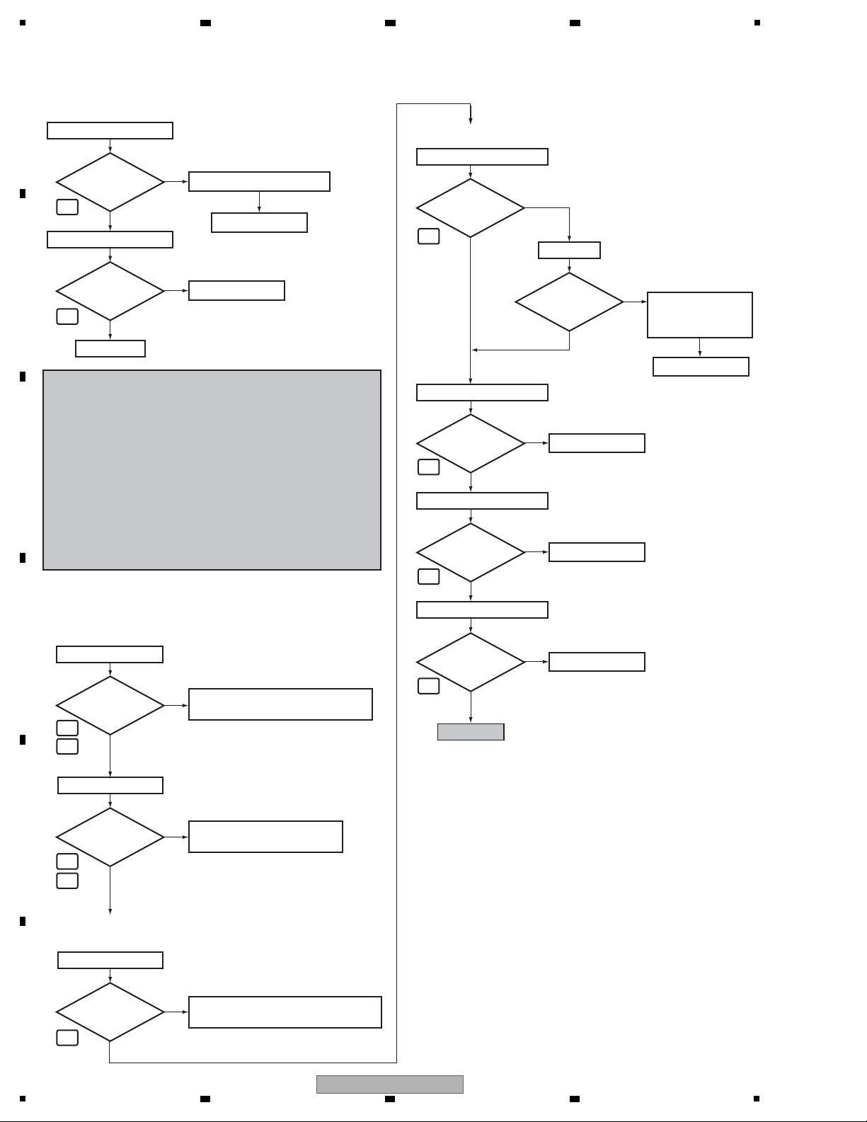
Step 4: DIR
Step 4-1
Check the parts and patterns
in the path.
Check the HDMI part, and the parts
and patterns in the path.
Check the OPTICAL IN JACK,
and parts and patterns in the path.
Check the path to
the IC1305
(Port expander).
R101, R102
OPT
Check that the S/PDIF signal is output.
Check that changes by pulling out and inserting the digital
input lines.
Can
observe the
digital signal
?
No
(0 V ⇔ 4 V)
Ye s
R122, R123
COAX
Can
observe the
digital signal
?
No
Ye s
Ye s
Check that it changes in the Playback and Pause modes of
the HDMI.
(0 V ⇔ 3.3 V)
IC101 (Pin 5)
From HDMI part
Can
observe the
digital signal
?
No
(1.65 V center, amplitude more than 0.2 Vp-p)
Step 3: X'tal
To Step 4
Check the X362 (side B).
Replace IC361.
Replace IC361.
Ye s
IC361 (Pins 1, 3, 5, 13)
IC361 (Pins 2, 4, 6, 12)
No
NG
Is there
a 24.576 MHz
input?
No
Is there
a 24.576 MHz
output?
Ye s
Replace IC101.
Ye s
No
Is there
a bit clock
output?
(0 V ⇔ 3.3 V)
To Step 5-3
Replace IC101.
(0 V ⇔ 3.3 V)
Ye s
No
Is there
a LR clock
output?
Replace IC101.
Ye s
R117
XDIRRST
No
NG
Is the
input signal
3.3 V?
Replace IC101.
(0 V ⇔ 3.3 V)
Ye s
No
Is there a
data output?
(0 V ⇔ 3.3 V)
IC101 (Pin 23) (or R110)
DIRMCLK (Master clock)
IC101 (Pin 24) (or R111)
DIRLRCK (LR clock)
IC101 (Pin 25) (or R112)
DIRADAT (Data)
IC101 (Pin 26) (or R113)
DIRBCK (Bit clock)
No
Ye s
Is there a
master clock
output?
Check that the data and clock signals are output.
• When the COAX or OPT is input, go to Step 4.
• When the HDMI (SPDIF path) is input, go to Step 4-1.
Used Source:
[dts HD High Resolution Audio], [dts HD LBR],
[Dolby Digital Plus], [2ch of 48kHz sampling rate or less],
[Other compression stream]
• When the HDMI (SACD) is input, go to Step 5-1.
Used Source: [SACD]
• When the HDMI (I2S path) is input, go to Step 5-2.
Used Source:
[dts HD Master Audio], [Dolby True HD],
[PCM or LPCM of 88.2kHz sampling rate or more],
[LPCM Multi ch]
• When the USB is input, go to Step 5-3.
9
9
10
11
13
14
15
16
17
18
19
B
1
2 3 4
C
D
E
F
26
1
VSX-1020-K
2 3 4
Page 27
5
To Step 6
Step 5: DSP input (digital)
Step 5-1
Step 5-3
Step 5-2
Step 5-4
Digital input of each CH when inputting the digital
signal with audio.
Ye s
IC301 (Pin 86) (or R326)
IC301 (Pin 85) (or R325)
IC301 (Pin 98) (or R332)
IC301 (Pin 99) (or R332)
LFE data (SACD)
No
Is there
a data input?
Ye s
Center data (SACD)
No
Is there
a data input?
Ye s
Surround L/R data
(Front R data (SACD))
No
Is there
a data input?
(0 V ⇔ 3.3 V)
(0 V ⇔ 3.3 V)
(0 V ⇔ 3.3 V)
Ye s
Center/LFE data
(Surround L data (SACD))
No
Is there
a data input?
(0 V ⇔ 3.3 V)
IC301 (Pin 100) (or R332)
Ye s
Surround Back L/R data
(Surround R data (SACD))
No
Is there
a data input?
(0 V ⇔ 3.3 V)
IC301 (Pin 89) (or R327)
IC301 (Pin 134)
Ye s
DSP0MCLK
No
Is there
a data input?
(0 V ⇔ 3.3 V)
Ye s
DSP1MCLK
No
Is there
a data input?
(0 V ⇔ 3.3 V)
IC301 (Pin 93) (or R330)
Ye s
S3BCK
No
Is there
a data input?
(0 V ⇔ 3.3 V)
IC301 (Pin 97) (or R332)
Ye s
Front L/R data
(Front L data (SACD))
No
Is there
a data input?
(0 V ⇔ 3.3 V)
IC301 (Pin 94) (or R331)
S3LRCK
No
Is there
a data input?
(0 V ⇔ 3.3 V)
Check the HDMI part, and the parts
and patterns in the path.
• When the USB is input, check the IC1300
and IC800, and the parts and patterns in
the path.
• When the HDMI I2S or HDMI SACD is input,
check the HDMI part, and the parts and
patterns in the path.
• When the COAX, OPT or HDMI SPDIF is
input, check the parts and patterns in the
path.
When the source is SACD, go to Step 6.
When the source is others, go to Step 5-4.
20
21
22
22
22
23
24
25
22
26
6 7 8
A
B
C
D
E
F
VSX-1020-K
5
6 7 8
27
Page 28
1
Step 6: DSP output (digital)
DAC Buffer
Digital output of each CH when inputting the digital
signal with audio.
Ye s
Center/LFE data
No
Is there
a data output?
Ye s
Surround L/R data
No
Is there
a data output?
Ye s
Front L/R data
No
Is there
a data output?
(0 V ⇔ 3.3 V)
(0 V ⇔ 3.3 V)
(0 V ⇔ 3.3 V)
Ye s
Surround Back L/R data
No
Is there
a data output?
(0 V ⇔ 3.3 V)
IC301 (Pin 123) (or R348)
IC301 (Pin 124) (or R348)
IC301 (Pin 125) (or R348)
IC301 (Pin 122) (or R348)
IC301 (Pin 123) (or R348)
IC301 (Pin 124) (or R348)
IC301 (Pin 125) (or R348)
IC301 (Pin 122) (or R348)
IC452 (Pin 16) (or R459)
IC452 (Pin 13) (or R458)
IC452 (Pin 11) (or R458)
Digital output of each CH when inputting the digital signal
(-∞ dB (no audio)).
Replace IC301.
There is a possibility
of the Boot error.
(Identification of the
defective part near
DSP is extremely
difficult.)
No
Ye s
Is the
voltage of
XDSP1RST at 3.3 V?
(Does it drop to 0V
periodically?)
Ye s
Replace IC301.
Surround L/R data
No
Is the output
0 V fixing?
Replace IC301.
Ye s
Center/LFE data
No
Is the output
0 V fixing?
Surround Back L/R data
Ye s
Replace IC301.
Front L/R data
No
Is the output
0 V fixing?
Ye s
Replace IC301.
No
Is the output
0 V fixing?
DA2MCLK (Master clock)
Ye s
Replace IC452.
No
Is there
a master clock
output?
Check that the clock signal is output.
(0 V ⇔ 3.3 V)
DA2BCK (Bit clock)
Ye s
Replace IC452.
No
Is there
a bit clock
output?
(0 V ⇔ 3.3 V)
(0 V ⇔ 3.3 V)
DA2LRCK (LR clock)
Ye s
Replace IC452.
No
Is there
a LR clock
output?
To Step 7
27
27
27
27
27
27
27
27
28
29
29
A
2 3 4
B
C
D
E
F
28
1
VSX-1020-K
2 3 4
Page 29
5
Replace IC651.
Ye s
CN501 (Pin 9)
Surround R out
No
Replace IC601.
Ye s
CN501 (Pin 7)
Front L out
No
Replace IC601.
Ye s
CN501 (Pin 5)
Front R out
No
Replace IC701.
Ye s
CN501 (Pin 15)
Center out
No
Replace IC701.
Ye s
CN501 (Pin 13)
Sub Woofer out
No
Replace IC751.
Ye s
CN501 (Pin 19)
Surround Back L out
No
Replace IC751.
Ye s
CN501 (Pin 17)
Surround Back R out
No
Replace IC651.
Ye s
CN501 (Pin 11)
Surround L out
No
Analog output of each CH when inputting the digital
signal (-∞ dB (no audio)).
End
Is the output
2.5 V fixing?
Is the output
2.5 V fixing?
Is the output
2.5 V fixing?
Is the output
2.5 V fixing?
Is the output
2.5 V fixing?
Is the output
2.5 V fixing?
Is the output
2.5 V fixing?
Is the output
2.5 V fixing?
Replace IC651.
Ye s
CN501 (Pin 9)
Surround R out
No
Is there
a data output?
Replace IC601.
Ye s
CN501 (Pin 7)
Front L out
No
Is there
a data output?
Replace IC601.
Ye s
CN501 (Pin 5)
Front R out
No
Is there
a data output?
Step 7: DAC output (analog)
Analog output of each CH when inputting the digital signal
with audio.
Replace IC701.
Ye s
CN501 (Pin 15)
Center out
No
Is there
a data output?
Replace IC701.
Ye s
CN501 (Pin 13)
Sub Woofer out
No
Is there
a data output?
Replace IC751.
Ye s
CN501 (Pin 19)
Surround Back L out
No
Is there
a data output?
Replace IC751.
Ye s
CN501 (Pin 17)
Surround Back R out
No
Is there
a data output?
Replace IC651.
Ye s
CN501 (Pin 11)
Surround L out
No
Is there
a data output?
34
34
34
34
34
34
34
34
34
34
34
34
34
34
34
34
6 7 8
A
B
C
D
5
6 7 8
VSX-1020-K
E
F
29
Page 30
1
Conditions for selecting SPDIF or I2S output (HDMI transmission)
pcm
fs (kHz) I2S (3 lines)SPDIFLayout
Compression DVD-V 48
Compression *.WAV 44
48
dts-CD 44
PCM 44
48
DVD-V
96 2ch
LPCM 44
Multi
48 2ch
Multi
88 2ch
Multi
DVD-A
96 2ch
Multi
176
Multi
192 2ch No
2ch No
No
No
No
No
No
2ch No
2ch No
2ch No
2ch No
2ch No
2ch No
No
No
Yes
Yes
Yes
Yes
Yes
Yes
Yes
Yes
Yes
Yes
Yes
Yes
Yes
Yes
Yes
Yes
Yes
Yes
Yes
Yes
Yes
Yes
Yes
Yes
Yes
Yes
2ch
Multi NA NA
NA NA
SACD
2ch (DSD)
Multi
No
No (DSD)
dts HD Master Audio
dts HD High Resolution Audio No
dts HD LBR No
Dolby TrueHD
No
No
Dolby Digital Plus No
Indistinguishable
A
2 3 4
B
C
D
E
F
30
VSX-1020-K
1
2 3 4
Page 31

5
To Step 2
Step 1: Power supply
CN1900 (Pins 1, 2)
Is the
voltage of around
13 V input
?
No
Ye s
V+13_UN
Check IC1900 and its
peripheral circuits.
<When no image is displayed after the unit is turned on, the HDMI LED on the front panel lights, and the HDMI or analog signal is input.>
• If conversion between 480i and 480p is not possible, it is most likely that IC800 is in failure. Check its peripheral circuits.
• Assume that the LCRs are neither in poor connection nor damaged.
• Analog video Convert (Ex.: S → COMPONENT) is satisfied by diagnosing the input and output.
• Although diagnosis is assumed to be performed from Side A, the wiring numbers on Side B are also described in the flowchart.
• This shows failure analysis for the HDMI & DVC Part of the D-MAIN Assy.
• The confirmation of peripheral circuits means mainly a power supply of IC, a sync signal, a existence of the input/output signal,
a conduction check and the appearance check of the bridges.
HDMI & DVC Block Troubleshooting
Check the MAIN Assy.
L1902
Is the
voltage of 5 V
output?
No
NG
Ye s
V+5_DDD
Check Q1900 and its periphery.
(Pins 1,2,5,6: around 9 V
Pin 3: around 6 V Square wave)
A
B
Check IC1900 and its
peripheral circuits.
R1916
Is the
voltage of around
5 V output?
No
NG
Ye s
V+5_HD
Check Q1900 and its periphery.
(Pins 1,2,5,6: around 9 V
Pin 3: around 6 V Square wave)
C
IC1100 (Pin 5) (side B)
Is the
voltage of around
3.3 V output
?
No
Ye s
V+3R3_EM_V
Check IC1100 and its peripheral
circuits.
Check IC1101 and its peripheral
circuits.
Check IC1102 and its peripheral
circuits.
Check IC1104 and its peripheral
circuits.
IC1101 (Pin 5) (side B)
Is the
voltage of around
3.3 V output
?
No
Ye s
V+3R3_EM_D
IC1102 (Pin 5) (side B)
Is the
voltage of around
2.5 V output
?
No
Ye s
V+2R5_EM
IC1104 (Pin 5) (side B)
Is the
voltage of around
1 V output
?
No
Ye s
V+1_EM
Check IC1930 and its
peripheral circuits.
L1931
Is the
voltage of around
3.3 V output
?
No
NG
Ye s
V+3R3_HHH
Check Q1930 and its periphery.
(Pin 1: around 7.5 V Square wave
Pins 5,6: around 16.5 V)
D
Check IC1930 and its
peripheral circuits.
L1932
Is the
voltage of around
1.8 V output
?
No
NG
Ye s
V+1R8_HHH
Check Q1931 and its periphery.
(Pin 1: around 5.5 V Square wave
Pins 7,8: around 16.5 V)
D
A
• The parts marked like in the following chart are located in "Check Points of the D-MAIN Assy."
6 7 8
A
B
C
D
E
5
VSX-1020-K
6 7 8
F
31
Page 32

1
Step 2: X'tal
Step 4: HDMI IN, HDMI OUT
To Step 3
Ye s
IC803 (Pins 5, 7) (side B)
IC1302 (Pin 7)
No
Is there
a 27 MHz
output?
No
Is there
a 36.864 MHz
output?
Ye s
E
To Step 4
CLK27EMMA, CLK27ABT
XHDTX1RST
F
JA1601-JA1604 (Pin 18)
Step 4-1: HDMI IN 1, 2, 3, 4
Is the voltage
around 5 V ?
No
Ye s
+5V
Check the soldering of JA1601JA1604 and the source equipment
connected in JA1601-JA1604.
JA1601-JA1604 (Pin 19)
Is the voltage
around 5 V ?
No
Ye s
Hot plug detect
Check IC1501 and its peripheral
circuits.
Check IC803 and its peripheral
circuits.
Step 3: RESET
Ye s
R931 (side B)
No
Is the
voltage "H"
(around 3.3 V)
?
XEMRST
Check the soldering and parts of
the path.
Ye s
R1851 (side B)
No
Is the
voltage "H"
(around 3.3 V)
?
XVSRST
Check the soldering and parts of
the path.
Ye s
IC1300 (Pin 91)
No
Is the
voltage "H"
(around 3.3 V)
?
XGARST
Check the soldering and parts of
the path.
Ye s
R1509
No
Is the
voltage "H"
(around 3.3 V)
?
Check the soldering and parts of
the path.
G
H
Ye s
R9018
No
Is the
voltage "H"
(around 3.3 V)
?
Check the soldering and parts of
the path.
Check IC1302 and its peripheral
circuits.
X1501 (Pins 1, 3)
No
Is there a
27 MHz input or
output?
Ye s
F
Q
JA1601-JA1604 (Pins 15,16)
Does
a signal output in
constant period
?
No
Ye s
DDC (SDA/SCL)
Check the soldering of JA1601JA1604.
JA1601-JA1604
(Pins 1,3,4,6,7,9,10,12)
Is there
0.5Vp-p in CLK
and DATA?
No
Ye s
TMDS signal
Check the soldering of JA1601JA1604.
Check X1501 and IC1501
and its peripheral circuits.
X1701 (Pins 1, 3)
No
Is there
a 28.63636 MHz
output?
Ye s
Check X1701 and IC1701
and its peripheral circuits.
R1270
No
Is there
a 48 MHz
signal?
Ye s
Check IC1251 and its peripheral
circuits.
A
A
2 3 4
B
C
D
E
F
32
VSX-1020-K
1
2 3 4
Page 33

To Step 4-2
JA9000 (Pin 18)
Is the voltage
around 5 V ?
No
Ye s
+5V
Check IC9001 and its peripheral
circuits.
JA9000 (Pin 19)
Is the voltage
around 5 V ?
No
Ye s
Hot plug detect
Check the sync equipment.
IC1800
IC9000
JA9000 (OUT 1)
(Pins 1,3,4,6,7,9,10,12)
Is there
0.5Vp-p in CLK
and DATA?
No
Ye s
TMDS signal
Video Scalar IC
HDMI Tx IC
Check the soldering of JA9000
and IC9000, and its peripheral
circuits.
NG
Check IC1501 and its
peripheral circuits.
J
K
L
M
Step 4-2: BD IN
To Step 4-3
JA9551 (Pin 18)
Is the voltage
around 5 V ?
No
Ye s
+5V
Check the soldering of JA9551.
Check the source equipment
connected in JA9551.
IC1501
Is the voltage
around 5 V ?
No
HDMI Rx IC
Check IC1601 and its peripheral
circuits.
JA9551 (Pins 15,16)
Does
a signal output in
constant period
?
No
Ye s
Ye s
DDC (SDA/SCL)
JA9551 (Pin 19)
Hot plug detect
Check the soldering of JA9551
and the path.
IC1601 (Pins 67,68,
70,71,73,74,76,77)
Is there
0.5Vp-p in CLK
and DATA?
No
Ye s
TMDS signal
JA9551
(Pins 1,3,4,6,7,9,10,12)
TMDS signal
Check IC1601 and its peripheral
circuits.
Is there
0.5Vp-p in CLK
and DATA?
No
Ye s
Check the soldering of JA9551
and the path.
N
I
B
A
A
A
IC1807,IC1808(side B),IC1809,
IC1810(side B),IC1811(side B)
(Pins 11-17)
Are signals
output?
No
Ye s
P** HSYNC VSYNC
PDE, PDCLK
Check IC1807-IC1811 and its
peripheral circuits.
Whole
diagram
HDMI OUT
5
6 7 8
A
B
C
D
E
F
VSX-1020-K
5
6 7 8
33
Page 34

1
Step 5: COMPONENT IN
Step 5-1: HDMI OUT (more than 480p)
CN1254 (Pin 14)
Is the voltage
"H" ?
No
Ye s
COMPDET
Check CN1254 and diagnose
the COMPONENT Assy.
P
CN1254 (Pins 2,4,6)
Is there a
analog video
signal? *
No
Ye s
Y_IN, CB_IN, CR_IN
* Diagnose it from the COMPONENT Assy side.
Check CN1254 and diagnose
the COMPONENT Assy.
Q1151,Q1155,Q1157
(Emitter), (side B)
Are the
signals output at
emitter?
No
Ye s
SG_A, SG_B, SG_C
Check Q1151, Q1155, Q1157 and
its peripheral circuits.
IC1701 (Pins 2,5-8,12-19,
25-28,59-62,64),R1706
(side B)
Are the
signals output?
No
Q** RXHSYNC, RXVSYNC, RXOCLK
Check IC1701 and its peripheral
circuits.
Ye s
IC1807,IC1808(side B),
IC1809,IC1810(side B),
IC1811(side B)
(Pins 11-17)
Are the
signals output?
No
P** HSYNC, VSYNC, PDE, PDCLK
Check IC1807-IC1811 and its
peripheral circuits.
Ye s
To Step 5-2
B
Step 4-3: HDMI IN 4 (Front IN)
To Step 5
CN1601 (Pin 18)
Is the voltage
around 5 V ?
No
NG
NG
Ye s
V+5_F
Check the soldering of CN1601.
Diagnose the F-HDMI Assy.
NG
Diagnose the F-HDMI Assy.
NG
Diagnose the F-HDMI Assy.
NG
Check IC1501 and its peripheral
circuits.
Check the source equipment.
CN1601 (Pins 15,16)
Does
a signal output in
constant period
?
No
Ye s
DDC (SDA/SCL)
Check the soldering of CN1601.
IC1601 (Pins 25,26,
28,29,31,32,34,35)
Is there
0.5Vp-p in CLK
and DATA?
No
Ye s
TMDS signal
IC1601 (Pins 48,49,51,
52,54,55,57,58)
TMDS signal
Check IC1601 and its peripheral
circuits.
Is there
0.5Vp-p in CLK
and DATA?
No
Ye s
Check the soldering between
IC1601 and CN1601.
CN1601
(Pins 1,3,4,6,7,9,10,12)
TMDS signal
Is there
0.5Vp-p in CLK
and DATA?
No
Ye s
Check the soldering of CN1601.
N
N
O
A
Whole
diagram
Analog IN, HDMI OUT
A
2 3 4
B
C
D
E
F
34
1
2 3 4
VSX-1020-K
Page 35

5
Step 5-2: Component IN, HDMI OUT (at 480i)
Q
P
Step 6: HDMI OUT
CN1254 (Pin 16)
Is there a
luminance
signal?
No
Ye s
A_VVYIN
Check CN1254 and diagnose
the COMPONENT Assy.
IC1701 (Pin 36) (side B)
Are there
color and luminance
signals?
No
Ye s
A_VVYIN
Check the soldering between
IC1701 and CN1254 and its
peripheral circuits.
IC1701 (Pins 2,5-8,59-62,
64),R1706 (side B)
Are the
signals output?
No
Ye s
Q** RXHSYNC, RXVSYNC,
RXOCLK
Check IC1701 and its peripheral
circuits.
IC1805 (Pins 3-9),
IC1806 (Pin 4) (side B)
Perform the same check items up to those
for IC1805 and IC1806 of Step 7.
Are the
signals output?
No
Ye s
Q16-23
VICLK
Check IC1805, IC1806 and its
peripheral circuits.
C
To Step 7
C
IC1801 (Pins 11-13),
IC1802, IC1803 (Pins 11-18),
IC1804 (Pin 4) (side B)
Are the
signals output?
No
Ye s
PHSYNC, PVSYNC, PDE
P**
PCLK
Check IC1801 to IC1804 and its
peripheral circuits.
IC800 (through hole)
(Pins E13,D13,E12,D12,E11,
D11,E10,D10,D15) (side B)
Are there
signals?
No
Ye s
VID0-7, VICLK
Check IC1805 and IC1806 and its
peripheral circuits.
Check the soldering.
Check IC800 and its peripheral
circuits. Check the soldering.
R872-R875,R878,R879,
R884-R887
Is there a
signal?
No
Ye s
VOD,VOCLK
Replace the D-MAIN Assy.
To Step 6
B
6 7 8
A
B
C
D
5
6 7 8
VSX-1020-K
E
F
35
Page 36

1
Step 7: COMPOSITE IN, HDMI OUT
CN1254 (Pin 16)
Is there a
signal?
No
Ye s
A_VVYIN
Check CN1254 and diagnose
the COMPONENT Assy.
P
IC1701 (Pin 36) (side B)
Is there a
signal?
No
Ye s
A_VVYIN
Check the soldering between
IC1701 and CN1254 and its
peripheral circuits.
IC1701 (Pins 2,5-8,59-62,
64),R1706 (side B)
Are the
signals output?
No
Ye s
Q** RXHSYNC, RXVSYNC,
RXOCLK
Check IC1701 and its peripheral
circuits.
IC1805 (Pins 3-9),
IC1806 (Pin 4) (side B)
Are the
signals output?
No
Q16-23
VICLK
Check IC1805, IC1806 and its
peripheral circuits.
Ye s
To Step 8
C
Step 8: COMPONENT IN
COMPONENT OUT
Perform the same check items up to
those for IC1701 and R1706 of Step 5-1.
R1214
Are there
signals?
No
NG
Ye s
A_VCYOUT_EM
R1219
A_VCBOUT_EM
R1224
A_VCROUT_EM
Replace the D-MAIN Assy.
P
Q
Q
IC1805 (Pins 3-9),
IC1806 (Pin 4) (side B)
Are the
signals output?
No
Ye s
Q16-23
VICLK
Note: When the connection is Composite S OUT, refer to the
diagnose of IC800 and later in steps 9 and 10.
Check the soldering between
IC1701 and IC1805, IC1806.
CN1254 (Pin 8)
Are there
signals?
No
Ye s
A_VCYOUT
CN1254 (Pin 10)
A_VCBOUT
CN1254 (Pin 12)
Diagnose the COMPONENT Assy.
A_VCROUT
Check the soldering and
connection of the CN1254.
Check Q1202 and its peripheral circuits.
Check Q1203 and its peripheral circuits.
Check Q1204 and its peripheral circuits.
Are there
signals?
No
Ye s
A_VCYOUT
A_VCBOUT
A_VCROUT
Replace Q1202, Q1203, Q1204
and its peripheral parts.
IC800 (through hole)
(Pins E13,D13,E12,D12,E11,
D11,E10,D10,D15) (side B)
Are there
signals?
No
Ye s
VID0-7, VICLK
Check IC1805, IC1806 and its
peripheral circuits.
Check IC800 and its peripheral
circuits.
DVC ON, Analog IN, OUT
A
2 3 4
B
C
D
E
F
36
1
2 3 4
VSX-1020-K
Page 37

5
Step 9: S IN, S OUT
To Step 10
Perform the same check items up to
those for IC1805 and IC1806 of Step 6.
R1203
Are there
signals?
No
NG
Ye s
A_VSYOUT_EM
R1209
A_VSCOUT_EM
Diagnose the IC800 (through hole) of Composite/S/
Component OUT and later.
Replace the D-MAIN Assy.
S
Q
Q
Q
Q
Note: When the connection is Composite OUT and Component OUT,
refer to the diagnose of IC800 and later in steps 8 and 10.
Note: When the connection is S Component OUT,
refer to the diagnose of IC800 and later in steps 8 and 9.
CN1254 (Pin 19)
Are there
signals?
No
Ye s
A_VSYOUT
CN1254 (Pin 21)
A_VSCOUT
Check the soldering and
connection of the CN1254.
P
Is there a
signal?
No
Ye s
CN1254 (Pin 8)
Diagnose the COMPONENT Assy.
A_VCYOUT
Check the soldering and
connection of the CN1254.
Check Q1202 and its peripheral circuits.
Q1200 Emitter
Q1201 Emitter
Are there
signals?
No
Ye s
Check Q1200, Q1201 and
its peripheral parts.
Is there a
signal?
No
Ye s
Replace Q1202 and its peripheral
parts.
IC800 (through hole)
(Pins E13,D13,E12,D12,E11,
D11,E10,D10,D15) (side B)
Are there
signals?
No
Ye s
VID0-7, VICLK
Check IC1805, IC1806 and its
peripheral circuits.
IC800 (through hole)
(Pins E13,D13,E12,D12,E11,
D11,E10,D10,D15) (side B)
Are there
signals?
No
Ye s
VID0-7, VICLK
Check IC1805, IC1806 and its
peripheral circuits.
Check IC800 and its peripheral
circuits. Check the soldering.
Step 10: COMPOSITE IN, COMPOSITE OUT
(at DVC ON)
Step 11: GUI/JPEG (USB)
Composite/S/Component OUT
Go to .
C
Step 12: GUI/JPEG (USB)
HDMI OUT
Perform the same check items up to
those for IC1805 and IC1806 of Step 7.
Is there a
signal?
No
Ye s
R1214
Replace the D-MAIN Assy.
A_VCYOUT_EM
A_VCYOUT
Check IC800 and its peripheral
circuits. Check the soldering.
NG
6 7 8
A
B
C
D
E
F
VSX-1020-K
5
6 7 8
37
Page 38

1
A
A
MC
BC
F
LR
S
C
SB
4
11
1
231
1
1
7
1
7
(121)
(118)
19
RR
A
B
1
4
L,L,L,L,L,L,L,
GNDCH3
GNDCH6
GNDCH4
R402
R403
L452
L453
D561
D562
C9401
C9403
C9404
L651
L652
C1900
D9000
C1901
C1903
C1904
Q1900
7
14
IC361
CN401
IC363
C1908
IC364
C1909
IC365
50
75
IC9000
IC1301
IC1302
IC1303
C1910
8
16
IC1304
D581
L281
C1911
8
16
IC1305
IC561
C1912
D582
D583
C1915
R621
C1917
R623
C1918
R1318
R434
L481
L482
L483
L291
C1345
R1320
D1900
IC9401
JA9401
C1930
8
16
IC1900
C1354
C1931
IC581
C1355
C1932
C1933
C603
C1934
Q1930
IC584
C1935
Q1931
7
14
IC391
C1936
C1937
C1938
C608
C1939
R1915
C419
R1916
R457
R458
C1941
C1942
C1943
C614
C9451
R467
C1952
C1953
C1954
C9460
C1956
D1932
C1957
C1958
R1930
D1934
L1815
R1931
L1816
R1932
L1817
R1933
R475
R476
R283
R477
R284
C1960
R478
R479
R671
R673
R480
D9451
D9452
C9477
R1368
R1369
R293
R294
R1949
R9455
IC9451
C9481
R1372
R1373
1950
1954
R494
C653
L101
L103
L104
C658
L105
L106
R9475
L302
R9476
L303
R9477
C664
L304
R9478
L501
L502
R9482
IC211
L701
L702
C487
C488
F9451
F9452
F9453
F9454
L521
CN1403 CN1404
4
7
14
IC241
X1300
R119
L551
R312
R120
L361
R316
R317
L363
R318
L364
L365
2
R126
L366
10
20
IC452
R127
L367
IC453
24
48
IC261
L751
CN301
L752
R320
R321
L561
L562
R132
D1403
D481
Q9701
D482
D483
D484
C101
R332
C102
R721
R723
R530
10
20
IC281
R1800
R1801
R1803
C114
R1804
L1300
C115
R1805
L1301
R1806
L1302
R1807
L1303
R1808
L1304
L9004
32
64
96
128
IC1800
R348
R1809
10
20
IC291
C505
R1810
C121
R1811
C122
R1812
JH1900
R1817
C703
R1818
R1819
C708
L9401
R552
L9402
L9403
R1823
R1824
R1825
R1828
L1900
C714
R1829
L1901
X9451
L1902
C522
L1903
C523
L1904
C330
C331
C527
R1830
C334
R1831
C335
R1832
R1833
R1834
R1835
R1836
R1837
R575
C539
F1800
R1845
F1801
R1846
F1802
C540
R1849
R771
R9357
R773
C543
R581
R582
R1850
L1930
L1931
L1932
L1933
C363
C753
D501
D502
C758
X361
C567
C568
71
12
24
36
48
IC101
72
L402
L403
L404
C764
L211
36
72
108
144
IC301
C579
L601
L602
C580
C581
C582
Q241
L241
C1301
Q1300
Q9000
Q9001
C1306
IC9402
L9404
R1952
R1953
CN1900
CN1903
C9407
C9408
C1902
C1913
C1343
C606
C1940
C612
C1944
C420
C618
C9472
C261
JA9451
C459
C656
CN482
JA481
C662
C668
JA101
JA102
JA103
JA104
CN501
C103
C1823
C1825
C506
C509
C706C712
C524
C718
C332
C552
C756
C762
C768
C577
C1307
KN481
C333
PC
1
1
1
5
15
10
15
1
5
1
5
1
5
50
55 60 65 70 75
80
15
10
15
20
1
5
1
15
10
5
1
15
10
5
1
1
1
1
1
5
1 5 10 15
15
1015
1
1
5
1
1
5
15
10
1
1
1
1
1
11 11
1
15
15 20
30 35 40
45 50 55
25
10
1 1
1 1
1
1
5
1
1
1
1
1 1
15
1
1
1
1 1 1
15 10
1520
5
1
1
5
101520
25
30
35
40
45
15
1 1
1
E
1
1
1
5
10
15
20
1
1 1
1 1 1
1 1
1 5 10 15 20 25 30
35 40 45 50 55 60
65 70 75 80
85 90 95
100 105 110 115 120 125
1
1
1
5
10
15
20
1 1
1
1
111
111
1
1
1
111
11111
1
1
1
1
1
1
1
1
15 10
15
20
25 30 35
40 45
1 5 10 15 20 25 30 35
40 45 50 55 60 65 70
75 80 85 90 95 100 105
110 115 120 125 130 135 140
E
E
1
E
1
1
1
15
15 15
10
1 5
1
11
15 15
20
10
N
D-MAIN ASSY
8: V+5_DACA
6: V+5_DAC
7: V+5_DACD
4
24
22
26
202325
21 1
2: V+5_DDD1
3: V+3R3_D
Check Points of the D-MAIN Assy
DSP Part HDMI Part
10
15
13
14
16
11
29
28
9
27
18
19
17
Whole
diagram
E
D
D
K
IC1800
IC1301
G
I
A: V+13_U
C: V+5_HD
B: V+5_DDD
5: V+1_DSPF
A
B
C
D
E
F
2 3 4
38
VSX-1020-K
1
2 3 4
Page 39

5
A
1
23
1
1
1
39
1
2191
41
1
14
30
30
DIGITAL MAIN
ASSY
ANP7740-6
5
C
D
RED
ASSY
DIGITAL MAIN
21
1
21
13
2200uF/6.3V
7020-06926-000-1S
GNDCH2
GNDCH1
GNDCH5
GNDCH7
D9000
C1901
R802
R803
R804
25
50
75
100
IC9000
C1718
JA9000
R813
R814
C1721
36
72
108
144
IC1501
CN800
R820
L1200
R821
L1201
R822
L1202
L1203
L1204
X1250
L1400
L1401
R834
R1525
R9225
R1526
R9226
R1527
R1528
R1529
C800
L1605
L1606
L1607
R1530
L1608
R1532
R1533
R1534
R1535
R1536
R1150
R1539
L1611
L1806
L1808
C814
C9460
R855
R857
R1930
L1815
R1931
L1816
R1932
L1817
R1933
C1576
C823
R1555
R1556
L1250
C834
L1251
R1949
R875
R1950
R879
R1954
C846
C849
C855
R94
R9477
R9478
C871
C874
F9451
F9452
F9453
IC800
IC801
C888
C1203
Q1200
Q1201
Q1202
Q1203
C1014
Q1204
CN1601
Q1400
Q1401
Q1402
Q1403
Q1405
Q1408
R1007
C1030
R1008
D1200
D1201
33
66
IC1001
C1032
R1202
R1010
R1011
D1400
R1015
D1401
R1016
D1402
Q9702
Q9703
R1406
R1020
R1021
14
7
IC1401
7
14
IC1406
7
14
IC1407
7
14
IC1408
20
40
60
80
IC1601
CN1259
JA1601 JA1602 JA1603 JA1604
C1252
R1807
R1808
L9004
96
128
IC
R1809
L9005
L9006
L9007
L9008
10
20
IC1807
R1810
R1811
10
20
IC1809
L1501
R1812
L1502
L9010
R1045
R
L1701
L1702
L1706
R1829
R1830
R1831
R1832
IC1250
IC1251
C9752
C917
C9753
C9754
R1263
F800
F801
F802
R1268
F1800
F1801
F1802
R1849
R1850
R1469
R1858
L1931
L1932
JA9551
R1862
R1865
R1866
R1867
R1868
R1871
R1872
Q801
L800
L802
L803
L804
L805
L807
L809
Q9000
Q9001
C1115
X1501
C1501
C1503
CN1900
C1705
C1716
C9033
C1720
C1150
C9049
C1745
C1940
C805
C1944
C809
C818
C820
C1577
C831
CN1400
CN1401
C1202
C1411
C1800
C1611
CN1250CN1252
C1823
CN1254
C1825
C1251
CN1405
LF
A30C5
[[ G ]]
15
10 15 20 25
30 35 40 45 50
55 60 65 70 75
80 85 90 95 100
1 5 10 15 20 25 30 35
40 45 50 55 60 65 70
75
80 85 90 95 100 105
110 115 120 125 130 135 140
15
10
1
1
1
1
1
1
1111
11111
1
1
1
111
1
1 1
11
1
1
30 35 40
1
1 1
1
1
1
A
1
1
5
E
E
E
E
E
E
E
EE
E
1
1 1
1
1 5 10 15 20 25 30
35404550556065
1
1
1
1
1
1
1
E
1
1
1
5
10
15
10
15
10
15
10
1 5 10 15 20
25 30 35 40
45 50 55 60
65 70 75 80
51
1 1
1 1
1
1510
90 95
100 105 110 115 120 125
1
111
15 10
1520
1 1
15 10
1520
1
1
1
1
1111
1
1
5
1
5
1
1
1
1
1
1
1
1
1
1 1
11
11
E
11
1
1
1
1
E
1
1
15
15 15
10
15
10
15 15
20
10
15 15
20
10
15 15
20
10
151015
20
25
30
35
SIDE A
IC800
L
H
F
F
M
IC9000
IC1809
J
IC1501
N
O
I
O
Q
P
IC1601
IC1807
A: V+13_UN
BD ININ 1IN 2IN 3IN 4
R1270
R884
R886
R875
R874
R887
R872
R885
R879
R873
R1214
R1209
R1203
Q1200
Q1201
Q1204
Q1202
Q1203
6 7 8
A
B
C
D
E
F
VSX-1020-K
5
6 7 8
39
Page 40

1
Item
[Error Indications]
[Purpose]
Error Indications When an Abnormality in The Amplifier System is Detected
[How to Enter Release Mode]
FL Display
LED
Flashes
NG
Count.
Detection
Method
Process After Detection Description / Remarks
“AMP DC”
(“DC output from
SP term”)
detection
Flashing
"AMP ERR"
for 3 seconds
MCACC
LED
DC
XDCERR
(Pin 80 of IC3004)
Detect "L"
1) Muting on, speaker relay off.
2) "AMP ERR" flashing
3) Shutdown after 3 seconds.
4) "MCACC" LED flashing
5) Power on is not acceptable.
To detect high DC output from amplifier damage
(defect status).
A process to protect speakers (for protection of
connected external devices).
For checking, refer to "How to enter release
mode" below.
If the DC detection port become “H” for
3 seconds, the unit will returns to normal
condition automatically.
“AMP overload”
detection.
N/A
iPod
LED
OL
XOLERR
(Pin 71 of IC3004)
Detect "L"
1) Muting on, speaker relay off.
2) Shutdown immediately.
3) "iPod" LED flashing
4) Power on is acceptable.
To detect overloading (abnormal status) with
low-load driving or a short circuit of the speaker
terminals (for protection of the amplifier).
“Over Heat”
detection.
Flashing
"AMP
OVERHEAT"
for 3 seconds
Center
Blue
LED
STMP
TEMPERR5
(Pin 72 of IC3004)
Detect "H"
1) Muting on, speaker relay off,
2) "OVERHEAT" flashing
3) Shutdown after 3 seconds.
4) "Center Blue" LED flashing
5) Power on is acceptable after
1 minute.
To detect overheat of inner tempareture.
"Abnormality DC
voltage of the
Digital power
supply" detection
N/A PQLS DERR
XVDDERR
(Pin 70 of IC3004)
Detect "L"
1) Muting on, speaker relay off.
2) Shutdown immediately.
3) "PQLS" LED flashing
4) Power on is acceptable.
To detect the abnormality voltage of Digital
power supply circuit for the D-MAIN Assy.
"USB Overload"
detection
“Over Current"
No Flashing
N/A N/A
USB ERR
(Pin M3 of IC800)
Detect "H"
1) Bass Power off
2) Display "Over Current"
3) Power on is acceptable
To detect the connected USB device is
overload. (over 500 mA)
“BT Adapter
overload”
detection.
"ADP
OVERLOAD"
No Flashing
N/A N/A
BTOL
(Pin N3 of IC800)
Detect "H"
1) Adapter port power off
2) Display "ADP OVERLOAD"
To detect the connected Blue Tooth Adapter
device is overload. (over 100 mA)
"HDCP of HDMI
Error"
detection
Flashes
“HDCP
ERR
OR”
for 5 seconds
N/A N/A
Read Register
value
1) Display "HDCP ERROR"
The monitor does not support HDCP type or
is in standby mode.
(Warning indication for HDMI Simplay)
"Analog Input
Over"
detection
During Standby mode, simultaneously press and hold the “TUNE ↓” and “MULTI-ZONE ON/OFF” keys for 5 seconds.
Errors upon detection of abnormalities in the amp system are indicated.
“OVER”
Icon lights
1 second
N/A N/A
DSP firmware
Detect
While the Icon lights 1 second,
when there is no ANALOG INPUT
OVER detection, the Icon stops
lighting and returns to normal
display.
To detect the over-input of the analog audio to
the A/D converter.
When the Icon lights frequently, output level of
the source equipment is high and a sound is
distorted. Turn on the Analog Att switch.
2 3 4
5.2 ERROR INDICATIONS
A
B
C
D
E
F
40
VSX-1020-K
1
2 3 4
Page 41

5
Key operation FL display
Display number of times
DC is detected.
Display number of times
OVERLOAD is detected.
Display number of times
COMBINATION is detected.
(Detects DC and OVERLOAD
simultaneously)
Display number of times
Power abnormality is
detected.
Display number of times
AMP overheat is
detected.
[↓]
[↑]
[↓]
[↑]
[↓]
[↑]
[↓]
[↑]
[↓]
[↑]
Display number of times
Digital Power abnormality is
detected.
Resetting the number of
times error is detected.
[↓]
[↑]
[↓]
[↑]
OL
:
DC
:
:
:
COM
XPRT
:
STMP
RESET
RESET
RESET
:
DERR
The numbers of detections for various protection processes are displayed.
[↓] : TUNE key
[↑] : TUNE key
[←] : PRESET key
[→] : PRESET key
During Standby mode, simultaneously press and hold “MULTI-ZONE ON/OFF” and “ENTER” keys for 5 seconds to enter
this mode.
Turn off the power to this unit by setting the main volume level to “---dB” and Multi-zone to “OFF”.
RESET
HOLD
CLEAR?
Resetting the number of times error is detected
Key operation FL display
↓
Continued
[ENTER]
[←][→]
[1] Detected protection history
[Purpose]
[How to enter/exit]
[Basic operations]
Front Panel Key
6 7 8
6. SERVICE MODE
6.1 TEST MODE
A
B
C
D
E
5
VSX-1020-K
6 7 8
F
41
Page 42

1
Key operation FL display
Display CEC(TEST) state.
Display FAN(TEST) state.
This function does not
work on this model.
USB Backup state
[↓]
[↑]
[↓]
[↑]
[↓]
[↑]
USB BAK
CEC
OFF
FAN
CEC
O N
OFF
HOLD
USB BAK
PLEASE WAIT
COMPLETE
SAV E?
USB BAK LOAD?
Display CEC(TEST) state.
Key operation FL display
↓
Change cyclically
[←][→]
Display USB backup state.
(A/V Receiver → USB)
(USB → A/V Receiver)
Key operation FL display
↓
Change cyclically
5 sec
SAVE or LOAD
is completed.
[←][→]
[←][→]
Key operation FL display
↓
Power OFF
(All zone OFF)
Change cyclically
Display accumulated
time & RESET.
[↓]
[↑]
CL?
RST
12345h20m
12345h 20m
0h 0m
HLD
Resetting the accumulated time
Key operation FL display
↓
Continued
[ENTER]
[ENTER]
[←][→]
CEC TEST : The function for making the HDMI output terminal to
output 1 kHz square wave. If the square wave is output,
the CEC line is considered to be normal.
[Description]
A
2 3 4
B
C
D
E
F
42
VSX-1020-K
1
2 3 4
Page 43

5
1. Discharging
(1) Unplug the power cord.
(2) Connect D5301 B+ and B- terminals, using resistor leads with 47 - 100 ohms (2 W or higher), for discharging.
∗ Discharging time: 30 - 60 seconds, depending on the level of resistance.
(3) Check that the voltage between the B+ and GND terminals, as well as that between the B- and GND terminals, is less
than 1 V, using a tester.
∗ Be sure to connect the GND terminal of the tester to the chassis.
∗ If the voltage is still 1 V or higher, repeat Step (2).
[1] MAIN Assy Capacitor (C5301, C5302)
[Procedures]
47 - 100 ohms
(2 W or higher)
B–
B+
C5301
D5301
D5301
C5302
Note:
(1) Even if the unit shown in the photos and illustrations in this manual may differ from your product, the
procedures described here are common.
(2) For performing the diagnosis shown below, the following jigs for service is required:
• 13P extension jig cable (GGD1669)
• 8P extension jig cable (GGD1670)
• 7P extension jig cable (GGD1671)
• 2P short connector jig (GGD1672)
• Board to board extension jig cable (GGD1675)
MAIN Assy
6 7 8
7. DISASSEMBLY
A
B
C
D
E
F
VSX-1020-K
5
6 7 8
43
Page 44

1
2. Notes on Ground Points Connection
Note:
The points marked below must be grounded when the rear panel is removed.
Before turning the unit ON, be sure to ground the marked points with the chassis. Or, you may short-circuit the ground points
on the solder surface, using pieces of wire.
Ground any one of these points.
Ground any one
of these points.
Ground any one of these points.
GND303
MAIN Assy
3. Screws for Chassis Back
A A A A A A
A
B
B
B
B
B
B
B B B B
B B B B
B B
B
B
BBB
B B
B
B
B B B B B B
B
B
B B
B
B
B B
A
B020930083B10-IL
B
BBT30P100FTB
A
2 3 4
B
C
D
E
F
44
1
VSX-1020-K
2 3 4
Page 45

5
4. Disassembly
[1] Front Panel Section and D-MAIN Assy
Remove the cabinet by removing the 10 screws.
(1) Remove the six screws. (BBZ30P080FTB)
(2) Remove the two screws. (BBZ30P080FTC)
(3) Remove the two screws. (BBZ30P080FTC)
(4) Unhook the two hooks.
(5) Remove the two screws. (BBZ30P080FTC)
(6) Arrange the front panel section as shown
in the photo below.
• Cable styling
1 1
2 2
3
4
6
5 5
3
4
1 1 1 1
• Bottom view
GUIDE-L Assy
GUIDE-R Assy
Front panel section
D-MAIN Assy
F-HDMI Assy
HDMI cable
Tape (80 × 40)
Clamp
6 7 8
A
B
C
D
5
VSX-1020-K
6 7 8
E
F
45
Page 46

1
[2] Heatsink Section
Remove the cabinet by removing the 10 screws.
Caution: Heatsink section in work becomes hot,
and be careful with it.
(1) Remove the seven screws. (BBZ30P080FTC)
(2) Remove the two screws. (BBZ30P080FTC)
(3) Disconnect the four connectors.
1
1
1
1
1
1 1
• Bottom view
3
3
3
3
AMP Assy
MAIN Assy
CP107
CP11
CP10
CN5001
2 2
GUIDE-L Assy GUIDE-R Assy
A
B
2 3 4
C
D
E
F
46
1
VSX-1020-K
2 3 4
Page 47

5
(4) Connect the three extension jig cables.
(5) Connect the 2P short connector jig.
(6) Rotate the heatsink section in the direction of
the arrow.
Heatsink section + AMP Assy
4
13P extension jig cable
(GGD1669)
4
8P extension jig cable
(GGD1670)
4
7P extension jig cable
(GGD1671)
5
2P short connector jig
(GGD1672)
6
CP11
∗
CP10
CN5001
MAIN Assy
CP107
Note ∗:
Please bind the jig cables (GGD1670 and
GGD1671) with tape to prevent an oscillation.
6 7 8
A
B
C
D
E
F
VSX-1020-K
5
6 7 8
47
Page 48

1
[3] AUDIO and COMPOSITE Assys
Remove the cabinet by removing the 10 screws.
(1) Remove the four felts.
(2) Remove the seven screws. (BBT30P100FTB)
(3) Remove the seven screws. (B020930083B10-IL)
(4) Remove the 32 screws. (BBT30P100FTB)
(5) Remove the chassis back.
(6) Remove the two screws. (BBZ30P080FTC)
(7) Reassembling the chassis back.
See “2. Notes on Ground Points Connection”.
(8) Arrange the unit as shown in the photo below.
(9) Connect the board to board extension jig cable.
(10) Connect the chassis back to the chassis
ground.
(11) Insert any insulation sheet between
top of heatsink and D-MAIN Assy.
• Rear view
D-MAIN Assy
×6
Bracket Bracket
2
2
22
6
6
2
3
×32
4
3
2
2
1 1 1 1
Chassis back
5
COMPONENT
Assy
MAIN Assy
COMPOSITE
Assy
AUDIO
Assy
8
7
9
10
11
Chassis back
Board to board extension
jig cable (GGD1675)
Insulation sheet
A
2 3 4
B
C
D
E
F
48
VSX-1020-K
1
2 3 4
Page 49

5
[4] MAIN Assy
(1) Remove the cabinet by removing the 10 screws.
(2) Remove the heatsink section.
(See steps [2] (1) to (5).)
(3) Remove the chassis back and D-MAIN Assy
etc. block. (See steps [3] (1) to (8).)
(1) Remove the five screws. (BBZ30P080FTC)
(2) Remove the three screws. (BBZ30P080FTC)
(3) Remove the seven screws. (B020030171B10-IL)
(4) Reassembling the D-MAIN Assy etc. block.
(5) Reassembling the chassis back.
Tighten back five screws (BBZ30P080FTC)
that were removed by the above step (1).
(It is necessary to fit these ICs to base chassis
in order to reduce heating of them even though
testing the following style.)
See “2. Notes on Ground Points Connection”.
(6) Arrange the unit as shown in the photo below.
(7) Connect the chassis back to the chassis ground.
(8) Insert any insulation sheet between base
chassis and MAIN Assy.
MAIN Assy
×4
2
3
3
3
3
3
3
3
1
1
2
2
MAIN Assy
6
7
8
5
Chassis back
Heatsink section
13P extension jig cable
(GGD1669)
8P extension jig cable
(GGD1670)
7P extension jig cable
(GGD1671)
2P short connector jig
(GGD1672)
MAIN Assy
CP107
Insulation sheet
6 7 8
A
B
C
D
E
F
VSX-1020-K
5
6 7 8
49
Page 50

1
MAIN com (EMMA), SUB com (EVENT) and DSP Flash ROM Update by USB Memory
and the Confirmation of the Version
[Preparations]
UPDATE PANEL Mode (Version update)
1. Copy the UPDATE FILE to the root directory of the USB Memory.
Note: NEVER copy several UPDATE FILES to the root directory of the USB Memory.
Copy only the corresponding UPDATE FILE.
Enter the UPDATE PANEL mode.
Check a current version.
2. Turn off the power to this unit by setting Multi-Zone to "OFF".
3. Connect the USB Memory to the USB terminal (A type) of the front panel.
1. While holding down "TUNE↑" key on the front panel, press "STANDBY ON/OFF" key and
moves to the UPDATE PANEL mode.
2. The updating process is as follows.
[Procedure]
Workflow
Check an updated version.
Turn the power off.
(Release the UPDATE PANEL mode.)
Update it.
Update completed.
(Turn the power OFF automatically.)
Updating process
Enter the UPDATE PANEL mode again.
Checking process
2 3 4
8. EACH SETTING AND ADJUSTMENT
8.1 HOW TO UPDATE FIRMWARE
A
B
C
D
E
F
50
1
2 3 4
VSX-1020-K
Page 51

5
Update Menu
UPDATE
Update Confirmation
UPDATE ?
N O
Update Confirmation
UPDATE ?
YES
File searching
PLEASE WAIT
Key operation FL display
[PRESET→]
or
[PRESET←]
[←]
[→]
[ENTER]
[ENTER]
UPDATE FILE searching
completed
Key operation FL display
[STANDBY ON/OFF]
[TUNE↑] +
MAIN com (EMMA) version is displayed.
Update Menu
[TUNE↓] or [TUNE↑]
[↓]
[↑]
Booting is completed
[TUNE↓] or [TUNE↑]
[↓]
[↑]
[TUNE↓] or [TUNE↑]
[↓]
[↑]
MAIN 1.000
POWER ON
UPDATE
SUB com (EVENT) version is displayed.
SUB 1.000
DSP version is displayed.
DSP 1.000
Front Panel Key
[↓] : TUNE key
[↑] : TUNE key
[←] : PRESET key
[→] : PRESET key
If no key is pressed within 10 seconds while booting UPDATE PANEL, the UPDATE PANEL is finished
and returns to the normal display. But the process does not become timeout and continues while "FILE searching"
or "Updating process".
6 7 8
A
B
C
D
E
F
VSX-1020-K
5
6 7 8
51
Page 52

1
Key operation FL display
DSP UPDATE completed
Updating process
MAIN com (EMMA) UPDATE
completed
SUB com (EVENT) UPDATE
completed
5 Second
UPDATE
Updating process
UPDATE
Update completion display
Power turns off automatically.
(All ZONE OFF)
Disconnect the USB MEMORY.
COMPLETE
Updating process
UPDATE
UPDATE FILE searching
completed
[Confirmation]
Enter UPDATE PANEL mode and check that the programs have been updated.
Update time is fluctuated by contents of the update. It will take about 15 minutes at the maximum.
(Actual time is from 2 minutes to 12 minutes.)
Time required for updating varies, because only the programs that require updating will be updated.
A
2 3 4
B
C
D
E
F
52
1
2 3 4
VSX-1020-K
Page 53

5
B
1. Idle Current Adjustment
• Adjustment Point and Measurement Points.... see fig1.
AMP ASSY
[Fig. 1]
SIDE A
Idle current
VR: V1201FL
TP1201FL 1 PIN
TEST POINT (–)
TP1201FL 3 PIN
TEST POINT (+)
TP1201SBR 3 PIN
TEST POINT (+)
TP1201SBR 1 PIN
TEST POINT (–)
TP1201SBL 3 PIN
TEST POINT (+)
TP1201SBL 1 PIN
TEST POINT (–)
TP1201FR 3 PIN
TEST POINT (+)
TP1201FR 1 PIN
TEST POINT (–)
Idle current
VR: V1201C
Idle current
VR: V1201SR
Idle current
VR: V1201FR
Idle current
VR: V1201SBL
Idle current
VR: V1201SBR
Idle current
VR: V1201SL
TP1201C 3 PIN
TEST POINT (+)
TP1201C 1 PIN
TEST POINT (–)
TP1201SR 3 PIN
TEST POINT (+)
TP1201SR 1 PIN
TEST POINT (–)
TP1201SL 1 PIN
TEST POINT (–)
TP1201SL 3 PIN
TEST POINT (+)
Measurement Points
Adjustment
Points
Procedure
V1201FL
TP1201FL 3PIN : TEST POINT(+)
TP1201FL 1PIN : TEST POINT(–)
1 Turn on the power.
2 Perform aging for one minute.
3 Connect a digital voltmeter to the measurement point.
4 Turn the adjustment VR so that the voltage becomes
in 2.0 mV ± 0.2 mV.
(Condition : No signal and no load)
V1201FL
TP1201FR 3PIN : TEST POINT(+)
TP1201FR 1PIN : TEST POINT(–)
V1201C
TP1201C 3PIN : TEST POINT(+)
TP1201C 1PIN : TEST POINT(–)
V1201SL
TP1201SL 3PIN : TEST POINT(+)
TP1201SL 1PIN : TEST POINT(–)
V1201SR
TP1201SR 3PIN : TEST POINT(+)
TP1201SR 1PIN : TEST POINT(–)
V1201SBL
TP1201SBL 3PIN : TEST POINT(+)
TP1201SBL 1PIN : TEST POINT(–)
V1201SBR
TP1201SBR 3PIN : TEST POINT(+)
TP1201SBR 1PIN : TEST POINT(–)
8.2 IDLE CURRENT ADJUSTMENT
6 7 8
A
B
C
D
E
F
5
6 7 8
VSX-1020-K
53
Page 54

1
NOTES: - Parts marked by “NSP” are generally unavailable because they are not in our Master Spare Parts List.
-
The > mark found on some component parts indicates the importance of the safety factor of the part.
Therefore, when replacing, be sure to use parts of identical designation.
-
Screws adjacent to b mark on product are used for disassembly.
-
For the applying amount of lubricants or glue, follow the instructions in this manual.
(In the case of no amount instructions, apply as you think it appropriate.)
Poly bag packing style
Cord AC
Tape (clear)
1/2
2/2
2 3 4
9. EXPLODED VIEWS AND PARTS LIST
A
9.1 PACKING SECTION
B
C
D
E
F
54
1
2 3 4
VSX-1020-K
Page 55

5
6 7 8
(1) PACKING SECTION PARTS LIST
Mark No. Description Part No.
1 Remote Control Unit 8300759500010-IL
NSP 2 Dry Cell Batteries G670001R50210-IL
(AAA size IEC R03)
3 AM Loop Antenna ATB7013
4FM Wire Antenna ADH7030
5Setup Microphone APM7008
(for Auto MCACC setup)(5 m)
6 iPod Cable L308102013010-IL
7 Operating Instructions See Contrast table (2)
8 Poly Bag 6330210059000-IL
A
NSP 9 Poly Bag 6337040062010-IL
10 Box, Gift See Contrast table (2)
11 Cushion, Snow 6230212784000-IL
12 Pe, Sheet 6327040059000-IL
NSP 13 Label VRW1629
NSP 14 Label Getter 1020U 5507000004560-IL
15 Sheet 5227000001050-IL
(2) CONTRAST TABLE
VSX-1020-K/UXCNCB and VSX-1025-K/CUXCN are constructed the same except for the following:
Mark No. Symbol and Description
7 Operating Instructions (En, Es) 5707000003280-IL Not used
7 Operating Instructions (En, Frca) Not used 5707000003320-IL
10 Box, Gift 6007211670010-IL 6007211670050-IL
VSX-1020-K
/UXCNCB
VSX-1025-K
/CUXCN
B
C
D
E
F
VSX-1020-K
5
6 7 8
55
Page 56

1
D
E
G
R
K
L
M
H
I
1/2
2/2
×
5
×
5
×
2
×
2
×
4
×
6
×
2
×
2
×
6
×
2
×
2
Nut
Nut
9.2 EXTERIOR SECTION
A
B
2 3 4
C
D
E
F
56
1
2 3 4
VSX-1020-K
Page 57

5
CONTACT SIDE
NON-CONTACT
SIDE
A
B
C
N
O
Q
J
K
S
F
P
Silicon grease
(GEM1057)
Silicon adhesive
(GYA1011)
×
7
×
5
×
5
×
3
×
2
×
3
×
2
×
14
×
21
×
4
×
4
×
4
×
4
×
4
×
38
×
4
×
4
×
6
×
7
×
7
×
5
×
7
×
6
×
2
×
2
6 7 8
A
B
C
D
E
5
VSX-1020-K
6 7 8
F
57
Page 58

1
(1) EXTERIOR SECTION PARTS LIST
Mark No. Description Part No.
1 MAIN Assy 7028069211010-IL
A
2 BRIDGE1 Assy 7028069213010-IL
3 GUIDE-L Assy 7028069214010-IL
4 GUIDE-R Assy 7028069215010-IL
5 GUIDE3 Assy 7028069218010-IL
2 3 4
No. Description Part No.
Mark
46 Cushion 4050211385000-IL
47 Cushion 4050211605000-IL
48 • • • • •
49 Cushion 4050211745000-IL
50 Cushion 4050212685000-IL
6 DISPLAY Assy See Contrast table (2)
7POWER SW Assy 7028069222010-IL
8 USB MTG Assy 7028069223010-IL
9 HDMI MTG Assy 7028069224010-IL
10 HEADPHONE Assy 7028069225010-IL
B
11 AMP Assy 7028069531010-IL
12 AUDIO Assy 7028069241010-IL
13 COMPONENT Assy 7028069242010-IL
14 COMPOSITE Assy 7028069243010-IL
15 BRIDGE2 Assy 7028069244010-IL
16 F-VIDEO Assy 7028069245010-IL
17 MIC Assy 7028069246010-IL
18 F-HDMI Assy 7028069251010-IL
19 D-MAIN Assy 7028069261010-IL
C
20 FM/AM TUNER Unit AXX7267
21 Posistor F320121021240-IL
> 22 Transistor (Q1202) J5011560Y0000-IL
> 23 Semi, TR/GE NPN 2SC (Q1203)J502396400010-IL
> 24 Transistor (Q1201) J5032390Y0000-IL
> 25 Power Trans. 8200960610650-IL
> 26 Cord Assy L068125101710-IL
27 Cable, HDMI L304201190020-IL
28 Cable, Flat Card 1.0M N711392313880-IL
D
29 Cable, Flat Card 1.25 N712111013880-IL
30 Pioneer Badge B XAM3006
51 Cushion 1020 4050213045000-IL
52 Supporter 4070001601010-IL
53 Cover See Contrast table (2)
54 Clamp MTG 4330000310000-IL
55 Clamp 4330040343010-IL
56 Guide 4350210451000-IL
57 Stopper 4380040162010-IL
58Window Display 5077212953100-IL
59 Knob 5080212361000-IL
60 Button 5090213741100-IL
61 Button 5Key 5090214311000-IL
62 Button 3Key 5090214331000-IL
63 Button 4Key 5090214351000-IL
64 • • • • •
NSP 65 Tape 1220210129300-IL
NSP 66 Tape 1220210879000-IL
67 Label Trans 5507000003270-IL
NSP 68 Label MAC Address 5507000004960-IL
69 Label Getter 1020U 5507000004560-IL
70 • • • • •
Screw BBT30P100FTB
71
72 Screw BBT40P080FTB
73 Screw BBZ30P080FTB
74 Screw BBZ30P080FTC
75 • • • • •
31 Sheet 1210210235000-IL
32 Sheet 1210211242000-IL
Sheet 1217211162000-IL
33
NSP 34 Heatsink Main 2120211718100-IL
35 Cabinet 3007211686000-IL
36 Panel Front See Contrast table (2)
NSP 37 Chassis Main 3200213436000-IL
E
38 Chassis Back See Contrast table (2)
39 Lens 3717211041000-IL
40 Foot See Contrast table (2)
41 Bracket 4010056906010-IL
42 Bracket 4010214716000-IL
43 Bracket 4010214726000-IL
44 Bracket 4010214736000-IL
45 Cushion 4050211365000-IL
F
58
1
2 3 4
76 Screw Tapping Assy B018230141H11-IL
77 Screw B020030171B10-IL
78 Screw, Tap Tite B020230063B10-IL
79 Screw, Tap Tite B020930083B10-IL
80Screw, Tap Tite B028130086B10-IL
81Screw B028940101B11-IL
82Screw 1500001456010-IL
VSX-1020-K
Page 59

5
6 7 8
(2) CONTRAST TABLE
VSX-1020-K/UXCNCB and VSX-1025-K/CUXCN are constructed the same except for the following:
Mark No. Symbol and Description
6 DISPLAY Assy 7028069221010-IL 70280692210C0-IL
36 Panel Front 3067214871000-IL 3067214871010-IL
38 Chassis Back 3207213476000-IL 3207213476010-IL
40 Foot 4007210391000-IL 4000210391000-IL
53 Cover 4317215111000-IL 4317215111020-IL
VSX-1020-K
/UXCNCB
VSX-1025-K
/CUXCN
A
B
C
D
E
F
VSX-1020-K
5
6 7 8
59
Page 60

1
A
A
AUDIO ASSY
(7028069241010-IL)
O
JP4001
P
CN7602
2 3 4
10. SCHEMATIC DIAGRAM
10.1 AUDIO ASSY
A
B
C
D
E
F
60
1
2 3 4
VSX-1020-K
Page 61

A
J
CN5001
F
CN7615
O
JP4001
F
CN7613
D
CN3652
: Audio Signal Route
5
6 7 8
A
B
C
D
E
F
VSX-1020-K
5
6 7 8
61
Page 62

1
B
B
COMPONENT ASSY
(7028069242010-IL)
N
2/12
CN1
N
2/12
CN1254
(CY)
(Y)
(Y)
(CR)
(CR)
(CB)
(CB)
(CR)
(CR)
(Y)
(CB)
(CB)
(CR)
(CR)
(CB)
(CY)
(VSY)
(VSC)
(VCR)
(VCR)
(VCB)
(VCB)
(VCY)
(VCY)
(VSY)
(VSC)
(CY)
(CR)
10.2 COMPONENT ASSY
A
2 3 4
B
C
D
E
F
62
1
2 3 4
VSX-1020-K
Page 63

5
B
C
CN8501
O
CN5002
E
J3652
O
CP6
N
2/12
CN1250
N
2/12
CN1252
: Video Signal Route
(Y)
(Y)
(Y)
(CB)
(CB)
(CB)
(CR)
(CR)
(CR)
6 7 8
A
B
C
D
E
5
VSX-1020-K
6 7 8
F
63
Page 64

1
C D
C
COMPOSITE ASSY (7028069243010-IL)
D
MIC ASSY (7028069246010-IL)
A
CN2105
B
CN8007
2 3 4
10.3 COMPOSITE, MIC, F-VIDEO and BRIDGE2 ASSYS
A
B
C
D
E
F
64
VSX-1020-K
1
2 3 4
Page 65

5
FEC
E
F-VIDEO ASSY (7028069245010-IL)
F
BRIDGE2 ASSY (7028069244010-IL)
B
CN8016
A
CN2106
A
CN2102
N
10/12
CN501
N
10/12
CN482
: Video Signal Route
: Audio Signal Route
6 7 8
A
B
C
D
E
F
VSX-1020-K
5
6 7 8
65
Page 66

1
G H I
G
F-HDMI ASSY
(7028069251010-IL)
H
USB MTG ASSY
(7028069223010-IL)
I
HDMI MTG ASSY
(7028069224010-IL)
FRONT
USB
N
2/12
CN1259
2 3 4
10.4 F-HDMI, USB MTG and HDMI MTG ASSYS
A
B
C
D
E
F
66
1
VSX-1020-K
2 3 4
Page 67

5
G
K
CP3002
2
N
5/12
CN1601
6 7 8
A
B
C
D
E
F
VSX-1020-K
5
6 7 8
67
Page 68

1
J
J
AMP ASSY
(7028069531010-IL)
A
CN2103
IDLE
CURRENT
IDLE
CURRENT
IDLE
CURRENT
IDLE
CURRENT
IDLE
CURRENT
(FL)(FL)
(SL)
(SL)(SL)
(SB
(SBL)
(C)(C)
(SBL)
(SBL)
(SBL)
(FL)
(SL)
10.5 AMP ASSY
A
B
2 3 4
C
D
E
F
68
1
2 3 4
VSX-1020-K
Page 69

5
J
O
CNT4
O
CP3
The > mark found on some component parts
indicates the importance of the safety factor of the part.
Therefore, when replacing, be sure to use parts
of identical designation.
IDLE
CURRENT
IDLE
CURRENT
: Audio Signal Route
(FL)
(FL)
(FL)
(SL)
(SL)
(SL)
(SBL)
(SBL)
(C)
(C)
(C)
(C)
(C)
(C)
(FL)
(SL)
6 7 8
A
B
C
D
E
VSX-1020-K
5
6 7 8
F
69
Page 70

1
K L
K
DISPLAY ASSY (7028069221010-IL: VSX-1020-K)
(70280692210C0-IL: VSX-1025-K)
L
HEADPHONE ASSY
(7028069225010-IL)
O
JH5301
2 3 4
10.6 DISPLAY, HEADPHONE and POWER SW ASSYS
A
B
C
D
E
F
70
1
VSX-1020-K
2 3 4
Page 71

5
MK
M
POWER SW ASSY
(7028069222010-IL)
N
3/12
CN1405
O
CN55GCN3005
6 7 8
A
B
C
D
E
F
VSX-1020-K
5
6 7 8
71
Page 72

1
N
1/12
A_VCRIN_EM
A_VSCIN_EM
A_VVYIN_EM
A_VCBIN_EM
XXMERR/RDSSCK
XMIRQ/RDSSI
XXMERR/RDSSCK
XRDSRST/XSIRST
CLK24.576
1u/6.3
150p/50
1000p/50
2.2u/10
330p/50
220p/50
100p/50
1000p/50
0.1u/16
2.2u/10
0.01u/16
DTL1106-A
DTL1106-A
DTL1106-A
F(1608)
F(1608)
F(1608)
V+2R5_EM
V+1R5_EM
V+1R5_EM_A
V+1_EM_PLL
V+1R5_EM_D
R9221
R9222
R9223
R9224
R9225
R9226
R9227
R9228
R9232
R957
2
1
4
3
6
5
8
7
2
1
4
3
6
5
8
7
reference=IC800
UPD61283F1-407LU2A-K
R883
R9288
JTDI
JTDO
JTMS
JTCL
HADRS5
HADRS7
HADRS6
JTDI
JTMS
JTDO
JTMRST
EDINT
JTCL
DDATA1
DDATA19
DDM0
DDATA0
DDQS0
DDATA16
DDATA17
DDATA2
DDATA18
DDATA3
DDATA6
DDATA7
DDATA22
DDATA21
DDATA20
DDATA4
DDATA5
DDM2
DDQS2
DDATA23
USBERR
USBPOW
DADRS5
DADRS12
DADRS9
DADRS4
DADRS7
DADRS11
DADRS6
DADRS8
DWE
DCLKO
DCS0B
DCAS
DCLKNO
DRAS
DBA1
DBA0
DADRS1
DADRS0
DADRS10
DDM1
DADRS3
DADRS2
DCKE
DDATA13
DDATA12
DDATA30
DDQS1
DDATA31
DDATA14
DDATA28
DDATA11
DDATA29
DDATA15
DDATA10
DDATA26
DDATA8
DDATA27
DDATA9
DDQS3
DDATA24
DDATA25
DDM3
VID7
VID6
VID5
VID4
VID3
VID2
VID1
VID0
D-
D+
EDINT
JTMRST
VSYNCO
HCS0
XRDGA
XWRGA
HSYNCO
A_VCBOUT_EM
A_VCYOUT_EM
A_VCROUT_EM
A_VSYOUT_EM
A_VSCOUT_EM
VICLK
VOD12
VOD0
VOD14
VOD1
VOD2
VOD4
VOCLK
VOD10
VOD11
VOD13
VOD15
HDRXINT
HDRXMUTE
X12VERR
RYCR
XAMUTE
XSBMUTE
XZ2MUTE
XZ3MUTE
HDTX2INT
AT1INTRQ
AT1D00
AT1D04
AT1D13
AT1D09
AT1D06
AT1D11
AT1D02
AT1D05
AT1D03
AT1D01
AT1D10
AT1D08
AT1D07
AT1IORDY
AT1D14
AT1D12
AT1DMARQ
AT1D15
HADRS23
RYB
RYAF
SDET
EM232TX
EM232RX
12VTRG1
XMIRQ/RDSSI
HDSDA
HDSCL
DSP2BUSY
DSP1BUSY
DSP1MUTE
EVSI
EVSO
EVSCK
VLSCK
USBCLK
XINTGA
HDTX1INT
DSP1BUSY
DSP2BUSY
DSP1MUTE
SIRX
XEMRST
EVREQI
EVREQO
XGARST
MUTEXM
UNLK
SITX
EVSO
EVSI
VLSCK
EVSCK
XVDECRST
12
VTRG2
DAZDB
AT0D05
AT0D02
AT0D04
AT0D03
AT0D00
AT0D01
AT0D06
AT0D07
AT0D08
AT0D09
AT0D10
AT0D11
AT0D12
AT0D13
AT0D14
AT0D15
AT0INTRQ
AT0DMARQ
AT0IORDY
HDATA9
HDATA14
HDATA13
HDATA7
HDATA12
HDATA15
HDATA8
HDATA11
HDATA10
HDATA5
HDATA3
HDATA6
HDATA4
HDATA0
HDATA1
HDATA2
HDRXSCDT
HADRS17
HADRS18
HADRS10
HADRS12
HADRS22
HADRS20
HADRS16
HADRS19
HADRS14
HADRS13
HADRS7
HADRS5
HADRS21
HADRS4
HADRS1
HADRS9
HADRS6
HADRS2
HADRS3
HADRS8
HADRS15
XINTGA
MUTEXM
HADRS11
COMPDET
XZ2MUTE
XZ3MUTE
XAMUTE
XSBMUTE
XVDECRST
CLK27EMMA
VOD3
VOD6
VOD5
VOD9
VOD8
VOD7
EMDE
TEMPERR
XRDSRST/XSIRST
X12VERR
CPSOMI
XCSGA
XCSLAN
HDMI5VDET
VSSCL
VSSDA
EMBCK
EMLRCK
EMADAT
HCS1
ZDZF
EMMCLK
NM
CN800
14FLT-SM2 (JST)
1
2
3
4
5
6
7
8
9
10
11
12
13
14
C874
MVG6.3VC100ME56TP
ACH7352-1
ACH7330-1
C831
MVG16VC10MD56TP
C849
MVG6.3VC100ME56TP
ACH7352-1
C846
MVG6.3VC100ME56TP
ACH7352-1
C834
MVG6.3VC100ME56TP
ACH7352-1
ACH7330-1
C805
MVG16VC10MD56TP
C855
MVG6.3VC100ME56TP
ACH7352-1
C823
MVG6.3VC100ME56TP
ACH7352-1
C818
MVG6.3VC220MF60TP
ACH7354-1
NM
C809
C820
MVG6.3VC220MF60TP
ACH7354-1
NM
C800
C814
MVG6.3VC100ME56TP
ACH7352-1
C854
1000p
C853
1u/6.3
C824
1u/6.3
C859
0.1u
C841
0.1u/10
C815
C835
1u/6.3
C843
0.1u/10
C829
0.1u/10
C871
2.2u/10
C882
1u/6.3
C890
CH
C828
0.1u/10
C830
0.1u/10
C826
0.1u/10
C887
1u/6.3
C872
0.1u/16
C851
C888
C885
CH
C884
CH
C852
0.1u/10
C836
1000p/50
C819
1u/6.3
C886
0.047u/10
C842
0.1u/10
C812
0.1u/10
C827
0.1u/10
C889
CH
C839
0.1u/10
C838
0.1u/10
C847
1u/6.3
C848
C873
C883
C840
0.1u/10
C821
1u/6.3
C833
1000p/50
C845 0.1u/10
C850
1u/6.3
C891
0.047u/10
C844
0.1u/10
C837 0.1u/10
C832
10u/6.3
(2125)
C816
1000p/50
C856
10u/6.3
(2125)
C858
1000p
C822
1000p
C825
1000p
C863
1000p
C861
1u/6.3
C862
0.1u
C864
1u/6.3
C865
0.1u
C866
1000p
C867
1000p
C868
1u/6.3
C869
0.1u
C870
1000p
C804
1000p
C808
NM
C860
0.01u/16
IC800
C811
0.1u
C801NMC803
0.1u
C807
0.1u
C817
1u/6.3
C880
C937
1u/6.3
C929
1000p/50
C928
0.1u/10
C927
9p/50
CH
C926
8p/50
CH
C813
0.1u/10
C875
0.1u/16
C806
1u/6.3
C857
1u/6.3
C938
1u/6.3
F803
DTL1106-A
3
2
1
L803
DTL1106-A
3
2
1
L804
DTL1106-A
3
2
1
L801
DTL1106-A
3
2
1
L805
DTL1106-A
3
2
1
L808
3
2
1
F801
3
2
1
L809
3
2
1
F800
DTL1106-A
3
2
1
F802
DTL1106-A
3
2
1
L802
DTL1106-A
3
2
1
L810
QTL1013-A
GNDD
GNDD
GNDD
GNDD
GNDD
GNDD
GNDD
GNDS
GNDD
GNDAD
GNDD
GNDS
GNDD
GNDD
GNDD
GNDD
GNDD
GNDAD
GNDD
IC803
SN74LVC3GU04DCTR
1A
1
3Y
2
2A
3
GND
45
2Y
6
3A
7
1Y
8
VCC
IC801
NJM12904V
3
4
2
1
8
IC801
NJM12904V
5
6
7
L800
15u
L807
15u
L806
39u
2SA1576A(QR)
Q801
2SA1576A(QR)
Q800
R857
47k
214
3
658
7
R855
47k
214
3
658
7
R834
10k
214
3
658
7
R927
10k
214
3
658
7
R926
47k
214
3
658
7
R822
1k
R845
33
R843
220
R814
100
D(1608)
R819
NM
R918
47k
R915
10k
R914
47k
R913
47k
R912
47k
R848
330
R813
43
D(1608)
R823
NM
R810
100
R811
47
R812
47
R928
10k
R929
10k
R930
47k
R931
10k
R932
10k
R933
10k
R935
47k
R936
47k
R937
47k
R850
47k
R851
47k
R852
47k
R817
22
R818
22
R836
47k
R820
470
R821
1k
R942
10k
R941
10k
R940
10k
R943
10k
R944
10k
R945
47k
R946
100k
R853
47k
R854
47k
R947
10k
R856
47k
R948
47k
R858
47k
R859
47k
R860
47k
R949
NM
R950
NM
R951
47k
R952
NM
R955
47k
R956
NM
R958
47k
R959
10k
R960
10k
R962
47k
R964
NM
R847
220
R802
NM
(1608)
R803
NM
(1608)
R804
0
(1608)
R829
NM
R815
43
D(1608)
R828
NM
R808
15k
R809
15k
R816
100
D(1608)
R844
330
R846
NM
R805
10k
R827
NM
R833
NM
R832
NM
R869
47k
R870
47k
R807
470
F
R871
220
R872
220
R873
220
R874
220
R878
22
R884
220
R885
220
R886
220
R887
220
R830
NM
R888
1M
R831
NM
R889
1k
R965
200
R842
NM
R849
33
R825
1k
R839
NM
R838
NM
R966
200
R904
NM
R903
NM
R837
NM
R835
10k
R892
10k
R893
10k
R894
10k
R895
47k
R897
22
R902
0
R901
0
TP809
TP827
TP810
TP811
TP812
TP815
TP822
TP814
TP807
TP806
TP821
TP819
TP833
TP820
TP805
TP808
TP816
TP801
TP818
TP817
TP800
TP804 TP803
TP802
TP832
VREF_D
V+1_EM_DEC
V+3R3_EM_V
V+3R3_EM_RF
V+3R3_EM_IO
V+2R5_EM
VREF_V
V+1_EM_CORE
VREF_V
V+1_EM_DLL
V+1_EM
V+3R3_EM_ADC
V+3R3_EM_D
V+3R3_EM_DEC
V+2R
V+3R3_EM_V
V+3R3_EM_V
V+3R3_EM_V
V+3R3_EM_DAC
V+1_EM
V+1_EM
V+3R3_EM_V
V+3R3_EM_V
V+3R3_EM_D
V+3R3_EM_D
V+3R3_EM_D
V+3R3_EM_D
V+3R3_EM_D
V+3R3_EM_D
V+3R3_EM_D
V+3R3_EM_D
V+3R3_EM_D
Analog Video In
12VTRG2
HDTX1INT
HDRXMUTE
HDRXINT
DV_EMIN
HDSDA
to USB
Z2VLSO
VLSO
JTRST
CLK27ABT
DV_EMOUT Analog Video Out
HDSCL
R976
0
R979
0
DA
R840
47k
GNDD
GNDD
GNDD
GNDD
R9212
NM
R9213
NM
R9250
22
R925122R925222R925322R925422R925522R925622R9257
22
R9258
22
R925922R926022R926122R926222R926322R926422R9265
22
R9266
56
R926756R926856R926956R927056R927156R927256R927356R927456R927556R927656R9277
56
R9278
56
R9279
56
R9280
56
R9281
56
R9282
56
R9283
56
R928456R9285
56
R9286
56
R9287
56
R9219
47k
R9220
47k
47k
47k
47k
47k
47k
214
3
658
7
47k
214
3
658
7
47k
47k
NM
47k
R875
220
R879
220
R876
47k
R877
47k
R9233
0
R9234NMR9235
22k
C939
0.01u/16
A1
GND(Digital)1
A2
DRASB
A3
DBA1
A4
DADD01
A5
DDQM1
A6
DQ13
A7
DQ11
A8
DQ08
A9
DIHM
A10
HTX_PDB
A11
HTX_D10
A12
HTX_D7
A13
HTX_CLK
A14
HTX_D3
A15
HTX_D0
A16
HTX_VSYNC
A17
HTX_DSDA
A18
SS0DOUT/GPIO46
A19
DA2_GND
A20
VAY(Video_DAC_CVBS/Y_out)
A21
RSET1(Video_DAC_RSET)
A22
VAR(Video_DAC_Pr/R_out)
A23
RSET0(Video_DAC_RSET)
A24
VAB(Video_DAC_Pb/B_out)
B1
DCLKB
B2
DCASB
B3
DBA0
B4
DADD00
B5
DADD03
B6
DQ12
B7
DQ15
B8
DQ09
B9
DDQM3
B10
HTX_RSEN
B11
HTX_D11
B12
HTX_D8
B13
HTX_D5
B14
HTX_D2
B15
HTX_DE
B16
HTX_CTL3
B17
HTX_DSCL
B18
SS0CKIN/GPIO44
B19
DA2_VDD3
B20
COMP1(Video_DAC_COMP)
B21
VAC(Video_DAC_C_out)
B22
VREF(Video_DAC_VREF)
B23
VAG(Video_DAC_Y_/G_out)
B24
COMP0(Video_DAC_COMP)
C1
DCLK
C2
DWEB
C3
DCS0B
C4
DADD10
C5
DADD02
C6
DDQS1
C7
DQ14
C8
DQ10
C9
DDQS3
C10
DILM
C11
HTX_CTL2
C12
HTX_D9
C13
HTX_D6
C14
HTX_D4
C15
HTX_D1
C16
HTX_HSYNC
C17
HTX_HPD
C18
SDA1/GPIO34
C19
AOBCK
C20
AIOMCLK0
C21
DA1_VDD3
C22
DA1_GND
C23
VCOMB(ADC(B)VCOM)
C24
VRTB(ADC(B)VRT)
D1
DADD06
D2
DADD07
D3
DADD08
D4
DADD11
D5
DCKE
D6
DQ30
D7
DQ28
D8
DQ26
D9
DQ24
D10
PHY_D7
D11
PHY_D5
D12
PHY_D3
D13
PHY_D1
D14
CTL1
D15
SCLK
D16
LPS
D17
SCL1/GPIO35
D18
SS0SB/GPIO47
D19
ATX
D20
AOLRCK
D21
VCOMY(ADC(Y)VCOM)
D22
VRTY(ADC(Y)VRT)
D23
ABI(ADC_B/G/Cb_in)
D24
VRBB(ADC(B)VRB)
E1
DADD04
E2
DADD05
E3
DCS1B
E4
DADD09
E5
DADD12
E6
DQ31
E7
DQ29
E8
DQ27
E9
DQ25
E10
PHY_D6
E11
PHY_D4
E12
PHY_D2
E13
PHY_D0
E14
CTL0
E15
LREQ
E16
LINKON
E17
SS0DIN/GPIO45
E18
AOD0
E19
AIBCK0
E20
AIBD0
E21
AIOMCLK1
E22
VRBY(ADC(Y)VRB)
E23
VCLY(ADC_PWM_VCL)
E24
AYI(ADC_CVBS/Y_in)
F1
DQ19
F2
DDQS0
F3
DDQM0
F4
DQ01
F5
DQ00
F6
DVREF
F7
DVDD25_1
F8
DVDD25_2
F9
DVDD25_3
F10
DVDD25_4
F11
DVDD25_5
F12
GND(Digital)2
F13
GND(Digital)3
F14
GND(Digital)4
F15
GND(Digital)5
F16
GND(Digital)6
F17
CSYNC/GPIO54
F18
IR_OUT/GPIO53
F19
AILRCK0
F20
IR_IN/GPIO52
F21
JTDI
F22
VRTR(ADC(R)VRT)
F23
ARI(ADC_R/B/Cr_in)
F24
VRBR(ADC(R)VRB)
G1
DQ16
G2
DQ17
G3
DQ18
G4
DQ03
G5
DQ02
G6
DVDD25_6
G7
DVDD25_7
G19
JTDO
G20
JTMS
G21
VCOMR(ADC(R)VCOM)
G22
VRTC(ADC(C)VRT)
G23
VRBC(ADC(C)VRB)
G24
ACI(ADC_C/G/R_in)
H1
DQ22
H2
DQ21
H3
DQ20
H4
DQ06
H5
DQ07
H6
DVDD25_8
H19
EDINT
H20
JTRST
H21
HLCI
H22
VCOMC(ADC(C)VCOM)
H23
AD2_VDD3(3.3V)
H24
AD2_GND
J1
DDQM2
J2
DDQS2
J3
DQ23
J4
DQ04
J5
DQ05
J6
DVDD25_9
J19
JTCL
J20
PH_VDD1(1.0V)
J21
HCBP
J22
FCBP
J23
PF_GND
J24
FSCI
K1
PLL_VDD(1.0V)
K2
CLK27AOUT
K3
CLKPWM0/GPIO60
K4
CLKPWM1/GPIO61
K5
SMCKOUT/SSCKIN
K6
DVDD25_10
K10
GND(Digital)7
K11
GND(Digital)8
K12
DVDD33_1
K13
DVDD33_2
K14
DVDD33_3
K15
DVDD33_4
K19
DGNDR
K20
HLCO
K21
HC_VDD3(3.3V)
K22
FC_VDD3(3.3V)
K23
FSCO
K24
PF_VDD1(1.0V)
L1
CLK27AIN
L2
PLL_GND
L3
CLK27BIN/GPIO62
L4
SMDOUT/SSDOUT
L5
SMDIN/SSDIN
L6
DLL_VDD
L10
GND(Digital)9
L11
DVDD33_5
L12
D
VDD33_6
L13
DVDD33_7
L14
DVDD33_8
L15
DVDD33_9
L19
SDA0
L20
NMI
L21
RSTSWB
L22
PH_GND
L23
AD1_VDD3(3.3V)
L24
CLK24OUT
M1
USB_DN0
M2
USB_DP0
M3
USB_H_OCI0/GPIO56
M4
AT1D00
M5
AT1INTRQ
M6
DLL_GND
M10
TEST_MODE
M11
FPIND
M12
LVSPOWD
M13
DVDD33_10
M14
DVDD33_11
M15
DVDD33_12
M19
SCL0
M20
RADD23/GPIO02
M21
RADD17
M22
RDATA09
M23
AD1_GND
M24
CLK24IN
N1
USB_CLKI/GPIO55
N2
USB_H_PPON0/GPIO57
N3
USB_D_VBUS/GPIO58
N4
AT1D13
N5
AT1D04
N6
GND(Digital)11
N10
DVDD10_1
N11
DVDD10_2
N12
DVDD10_3
N13
DVDD10_4
N14
DVDD33_13
N15
DVDD33R
N19
RADD24/GPIO03
N20
RDATA14
N21
RADD18
N22
RDATA13
N23
RDATA07
N24
GND(Digital)10
P1
USB_D_DN0
P2
USB_D_DP0
P3
USB_D_CONNECT/GPIO59
P4
AT1D06
P5
AT1D09
P6
GND(Digital)12
P10
DVDD10_5
P11
DVDD10_6
P12
DVDD10_7
P13
AT0D06
P14
AT0DIOWB
P15
AT0D10
P19
RADD25/GPIO04
P20
RADD00/GPIO01
P21
RDATA12
P22
RADD10
P23
RADD12
P24
RADD22
R1
AT1D01
R2
AT1D03
R3
AT1D05
R4
AT1D02
R5
AT1D11
R6
GND(Digital)13
R10
DVDD10_8
R11
DVDD10_9
R12
AT0DIORB
R13
AT0D08
R14
AT0D12
R15
AT0D07
R19
GCSB2/GPIO05
R20
GRDYB/GPIO07
R21
RDATA15
R22
RADD20
R23
RDATA08
R24
RADD16
T1
AT1D07
T2
AT1D08
T3
AT1D10
T4
AT1CS0B
T5
AT1DA2
T6
GND(Digital)14
T10
DVDD10_10
T11
DVDD10_11
T12
AT0D05
T13
AT0IORDY
T14
AT0D15
T15
AT0DMARQ
T19
GCSB3/GPIO06
T20
GCSB1
T21
RDATA11
T22
RDATA10
T23
RADD19
T24
RDATA05
U1
AT1D12
U2
AT1D14
U3
AT1DA0
U4
AT1IORDY
U5
AT1DIOWB
U6
GND(Digital)15
U10
AT0DA1
U11
AT0D01
U12
AT0D02
U13
AT0D11
U14
AT0DA2
U15
AT0D13
U19
CTS0B/GPIO37
U20
RADD14
U21
RADD13
U22
RADD11
U23
RDATA03
U24
RDATA06
V1
AT1DIORB
V2
AT1DMACKB
V3
AT1CS1B
V4
AT1RESETB
V5
AT1DMARQ
V6
GND(Digital)16
V10
AT0D09
V11
AT0D04
V12
AT0INTRQ
V13
AT0RESETB
V14
AT0D00
V15
AT0DMACKB
V19
RTS0B/GPIO36
V20
GCSB0
V21
RADD07
V22
RDATA04
V23
RADD05
V24
FCSB0
W1
AT1D15
W2
AT1DA1
W3
MD9
W4
MD6
W5
MD8
W6
DVDD15_1
W10
GND(Digital)17
W11
AT0CS1B
W12
AT0CS0B
W13
AT0D14
W14
AT0DA0
W15
AT0D03
W19
SP1REQB/GPIO11
W20
RADD21
W21
RDATA00
W22
FOEB/GOEB
W23
RADD04
W24
FCSB1
Y1
MD15
Y2
MD11
Y3
MD0
Y4
MD7
Y5
MD10
Y6
DVDD15_2
Y10
GND(Digital)18
Y11
GND(Digital)19
Y12
AGND1
Y13
AGND2
Y14
AGND3
Y15
AGND4
Y19
SP0REQB/GPIO33
Y20
RADD01
Y21
RDATA01
Y22
RADD09
Y23
RADD06
Y24
RADD02
AA1
MD14
AA2
LDQM
AA3
MD5
AA4
MD1
AA5
MD3
AA6
DVDD15_3
AA19
RTS1B/GPIO40
AA20
SP0CLK/GPIO31
AA21
RDATA02
AA22
RADD03
AA23
RADD08
AA24
FWEB/GWEB
AB1
MD2
AB2
UDQM
AB3
MD4
AB4
MCLKOUT
AB5
MD13
AB6
DVDD15_4
AB19
CTS1B/GPIO41
AB20
SP0EN/GPIO21
AB21
SP1CLK/GPIO08
AB22
SP0STRT/GPIO32
AB23
SP1STRT/GPIO10
AB24
RADD15
AC1
MA9
AC2
MD12
AC3
MA10
AC4
MCKE
AC5
MA7
AC6
PDIAGB
AC19
MONI3/SWRF4/RFPM3
AC20
SP1EN/GPIO09
AC21
SP1DAT2/GPIO14
AC22
SP0DAT7/GPIO29
AC23
SP1DAT7/GPIO19
AC24
SP0DAT6/GPIO28
AD1
MA6
AD2
MA5
AD3
MA1
AD4
MA8
AD5
MBA
AD6
DASPB
AD7
HIOCS16B
AD8
SFSO
AD9
SFSCK
AD10
SFSI
AD11
SFCS0B
AD12
AVDD15
AD13
AVDD33_1
AD14
AVDD33_2
AD15
AVDD33_3
AD16
AVDD33_4
AD17
TEST1
AD18
MONI1/RFPM1
AD19
MONI2/RFPM2
AD20
SP1ERRB/GPIO20
AD21
SP1DAT6/GPIO18
AD22
SP1DAT5/GPIO17
AD23
SP0DAT5/GPIO27
AD24
SP0DAT3/GPIO25
AE1
XA1
AE2
CASB
AE3
MA0
AE4
MA4
AE5
MA3
AE6
PB4
AE7
PB1
AE8
RLDM
AE9
WLD
AE10
WLDM
AE11
PLED
AE12
CWAGC
AE13
CWHP
AE14
CAD
AE15
CBC
AE16
CTEC
AE17
CRC
AE18
CBHLPP/CRAPC
AE19
ADIN/LE/RFP4
AE20
SP0ERRB/GPIO30
AE21
SP0DAT2/GPIO24
AE22
SP1DAT3/GPIO15
AE23
SP1DAT4/GPIO16
AE24
SP0DAT1/GPIO23
AF1
XA2
AF2
WEB
AF3
MA2
AF4
RASB
AF5
PB2
AF6
PB5
AF7
PB7
AF8
RLD
AF9
REF16
AF10
VREFIO
AF11
P2LD
AF12
CADO
AF13
CBHWBL/CID
AF14
CAMIRR
AF15
CBPD
AF16
CAGC
AF17
CAGC2
AF18
CEQDC
AF19
FEO/LE/SWRF2/SWRF4/RFP5
AF20
TEO/LE/SWRF1/SWRF3/RFP6
AF21
TxD0B
AF22
RxD0B
AF23
SP0DAT4/GPIO26
AF24
SP0DAT0/GPIO22
AG1
PB3
AG2
PA0
AG3
PA4
AG4
PB0
AG5
PB6
AG6
PA3
AG7
PA5
AG8
PDIN
AG9
FPDVI
AG10
FPDVO
AG11
CREG
AG12
CBCO
AG13
WALPF
AG14
CMIRR
AG15
CBBD
AG16
RFEQOM
AG17
RFEQOP
AG18
RFO
AG19
CDEF
AG20
FG
AG21
RFT1/SWRF1/RFP1
AG22
RxD1B/GPIO38
AG23
TxD1B/GPIO39
AG24
SP1DAT1/GPIO13
AH1
PKPULSE1M
AH2
PKPULSE1P
AH3
WRPULSEM
AH4
WRPULSEP
AH5
HFONP
AH6
PA7
AH7
PA2
AH8
H1/FOM
AH9
G1/FOP
AH10
F1
AH11
E1
AH12
RFP
AH13
ASY
AH14
FCEFM2
AH15
PCEFM2
AH16
RFI_M
AH17
RFI_P
AH18
AGCIN
AH19
CDEF2
AH20
TDRV
AH21
FDRV
AH22
RFT2/SWRF2/RFP2
AH23
RXD2B/GPIO42
AH24
SP1DAT0/GPIO12
AJ1
OFPULSE/WRCKP
AJ2
OFPULSE/WRCKM
AJ3
PKPULSE2/NRZIM
AJ4
PKPULSE2/NRZIP
AJ5
HFONM
AJ6
PA1
AJ7
PA6
AJ8
D1
AJ9
C1
AJ10
B1
AJ11
A1
AJ12
RFN
AJ13
EFM
AJ14
FCEFM1
AJ15
PCEFM1
AJ16
EXTR
AJ17
CEQ
AJ18
REQ
AJ19
DAOUT
AJ20
SDRV2
AJ21
SDRV1
AJ22
MDRV
AJ23
WRFM/SWRF3/RFP
AJ24
TXD2B/GPIO43
R806
680
F
R882
47k
22
R9301
0
R9332
0
R9300
0
R9333
0
R9331
0
DAZDB
R891
0
R890
0
C1082
0.1u/10
R1083
NM
L1081
QTL1013-A
R1081
220
C1081
470p/50
GNDD
CLK24.576IN
R1082
47
V+3R3_EM_D
R9236
47
NM
R9289
NM
R9290
NM
R9291
NM
R9292
NM
C881
NM
V+3R3_EM_D
BTOL
R9651
47k
R9653
47
V+3R3_EM_V
R9652
47k
R9658
NM
XMICDET
XHPDET
R5961
10k
R5962
10k
R5963
10k
X801
ASS7106-1
27MHz
FA-238 27MHz CL=7pF (EPSON)
1
1
GND1
2
GND2
43
3
R9661
100
IC1081
SN74AHC1G08DCK
A
1
B
2
GND3Y
4
5
VCC
R9664
47k
R5964
47k
R916
1k
R917
1k
TRST
EJSNGEN
TDI
GND
TDO
DINTEN
TMS
GND
TCK
GND
RST
JTSEL
DINT
V+3
EJTAG
fsc BPFHCL BPF
to DDR SDRAM
AB
1
1
1
1
1
MAIN LSI
Proto only
N 10/12
N 2/12
N 5/12
N 5/12
N 3/12
N 2/12
N 6/12
N 3/12,5/12-11/12
N 9/12
N 2/12
N 2/12
N 6/12
N 3/12
N 2/12
N 3/12
N 3/12
10.7 D-MAIN ASSY (1/12)
A
2 3 4
B
C
D
E
F
72
1
2 3 4
VSX-1020-K
Page 73

5
N
1/12
A-a A-b
Large size
SCH diagram
Guide page
Detailed page
A-a A-b
A-a A-b
XMIRQ/RDSSI
XXMERR/RDSSCK
XRDSRST/XSIRST
0.01u/16
0.01u/16
1000p/50
1000p/50
0.01u/16
0.1u/16
0.01u/16
0.1u/16
0.1u/16
0.1u/16
0.1u/16
1000p/50
1000p/50
1000p/50
1000p/50
NM
2125
10u/6.3
RESET#
WP#/ACC
RY/BY#
DQ15/A-1
F(1608)
10u/6.3
R9227
R9228
R9232
R957
A15
A14
A13
A12
A11
A10
A9
A8
A19
A20
WE#
RESET#
NC
WP#/ACC
RY/BY#
A18
A17
A7
A6
A5
A4
A3
A2
A1
A0
CE#
VSS1
OE#
DQ0
DQ8
DQ1
DQ9
DQ2
DQ10
DQ3
DQ11
VCC
DQ4
DQ12
DQ5
DQ13
DQ6
DQ14
DQ7
DQ15/A-1
VSS2
BYTE#
A16
DADRS9
DADRS0
DADRS1
DADRS10
DADRS4
DADRS6
DADRS3
DADRS7
DADRS11
DADRS2
DADRS8
DRAS
DWE
DCS0B
DCAS
DCLKNO
DCLKO
DADRS12
DBA0
DBA1
TADRS5
TADRS4
TADRS6
TADRS10
TADRS11
TADRS2
TADRS7
TADRS12
TWE
TCS
DDQS3
TADRS9
HADRS14
HADRS16
HADRS15
HADRS18
HADRS19
HADRS13
HDATA3
HDATA11
HADRS3
HADRS4
HADRS5
HADRS6
HADRS7
XWRGA
HADRS9
HADRS10
HADRS12
HDATA5
HDATA13
HDATA14
HDATA6
HDATA15
HDATA7
HADRS10
HADRS8
HADRS4
HADRS3
HADRS2
DADRS5
TADRS8
HADRS21
HADRS11
HADRS8
HDATA3
HDATA11
HDATA10
HDATA2
HDATA9
HDATA1
HDATA8
HDATA0
HDATA4
HDATA12
DDM1
TWE
TCAS
TRAS
TCS
TBA0
TBA1
TADRS10
TADRS0
TADRS1
TADRS2
TADRS3
DDQS1
DDATA15
DDATA14
DDATA13
DDATA12
DDATA11
DDATA10
DDATA9
DDATA8
TADRS3
TADRS2
TADRS1
TADRS0
TADRS10
TBA1
TBA0
TCS
TRAS
TCAS
TWE
DDM0
DDQS0
DDATA7
DDATA6
DDATA5
DDATA4
DDATA3
DDATA2
DDATA1
DDATA0
DDM3
TADRS12
TADRS11
TADRS9
TADRS8
TADRS7
TADRS6
TADRS5
TADRS4
DDATA24
DDATA25
DDATA26
DDATA27
DDATA28
DDATA29
DDATA30
DDATA31
TADRS4
TADRS5
TADRS6
TADRS7
TADRS8
TADRS9
TADRS11
TADRS12
DDM2
DDQS2
DDATA16
DDATA17
DDATA18
DDATA19
DDATA20
DDATA21
DDATA22
DDATA23
HADRS1
HCS0
XRDGA
HDATA0
HDATA8
HDATA1
HDATA9
HDATA2
HDATA10
HDATA4
HDATA12
HDATA5
HDATA13
HDATA6
HDATA14
HDATA7
HDATA15
HADRS17
HADRS2
HADRS19
HADRS18
DCKE
TCLKNO
TCLKO
TCLKNO
TCLKO
TCLKO
TCLKNO
TADRS3
TCAS
TBA0
TRAS
AT1D07
AT1D08
AT1D06
AT1D09
AT1D05
AT1D10
AT1D04
AT1D11
AT1D03
AT1D12
AT1D02
AT1D13
AT1D01
AT1D14
AT1D00
AT1D15
AT1INTRQ
AT1IORDY
TADRS1
TADRS0
TBA1
HADRS12
EM232TX
EM232RX
12VTRG1
SDET
COMPDET
AT1DMARQ
DSP1BUSY
DSP2BUSY
DSP1MUTE
SIRX
RYCR
RYB
RYAF
SITX
DAZDB
AT0D07
AT0D08
AT0D06
AT0D09
AT0D05
AT0D10
AT0D04
AT0D11
AT0D03
AT0D12
AT0D02
AT0D13
AT0D01
AT0D14
AT0D00
AT0D15
AT0DMARQ
AT0IORDY
AT0INTRQ
12VTRG1
HADRS11
HADRS20
EM232TX
EM232RX
XZ2MUTE
XZ3MUTE
XAMUTE
XSBMUTE
XVDECRST
X12VERR
RYFH
HADRS1
HADRS13
HADRS19
HADRS11
HDATA2
HADRS18 HDATA9
HDATA1
HDATA8
HADRS9
HADRS14
HDATA0
HADRS2
XWRGA
HADRS8
XRDGA
HDATA13
HADRS17
HADRS15
HADRS7
HDATA5
HDATA15
HADRS16
HADRS6
HDATA12
HDATA7
HADRS5
HDATA4
HADRS4
HDATA14
HDATA10
HDATA6
HADRS3
HDATA11
HDATA3
HADRS12
HADRS10
HCS1
HADRS20
HADRS21
HADRS22
HADRS20
HADRS22
ZDZF
C874
MVG6.3VC100ME56TP
ACH7352-1
C1014
MVG6.3VC100ME56TP
ACH7352-1
C1032
MVG6.3VC100ME56TP
ACH7352-1
C1000
NM
C1001
1u/6.3
C1003
1u/6.3
C1007
1u/6.3
C1016
1u/6.3
C1017
1u/6.3
C1020
1u/6.3
C1022
1u/6.3
C1026
1u/6.3
C1018
1u/6.3
C1019
1u/6.3
C877
NM
C1015
1u/6.3
C1024
C1023
C1027
YB
C1006
YB
C1005
C1013
C878
2.2u/10
C1004
C1002
C1010
C1011
0.1u/16
C1012
C1053
1u/6.3
C876
C1008
YB
C1009
YB
C1025
YB
C1050
1000p/50
C1028
YB
C879
10u/6.3
(2125)
C917
NM
10u(2125)
C900
C1051
1u/6.3
C1031
(2125)
C1052
0.1u/16
C1029
0.1u/16
C1021
0.1u/16
C875
0.1u/16
GNDD GNDS
GNDS
GNDD
GNDD
GNDD
GNDD
GNDD
GNDD
GNDD
GNDD
GNDD
GNDD
GNDD
GNDD
GNDD
IC1050
MX29LV640ETTI-70G
MX29LV640ETTI-70G-K
A15
1
A14
2
A13
3
A12
4
5
A11
6
A10
7
A9
8
A8
9
A19
10
A20
11
WE#
12
13
A21
14
15
16
A18
17
A17
18
A7
19
A6
20
A5
21
A4
22
A3
23
A2
24
A1
25
A0
26
CE#
27
VSS1
28
OE#
29
DQ0
30
DQ8
31
DQ1
32
DQ9
33
DQ2
34
DQ10
35
DQ3
36
DQ11
37
VCC
38
DQ4
39
DQ12
40
DQ5
41
DQ13
42
DQ6
43
DQ14
44
DQ7
45
46
VSS2
47
BYTE#
48
A16
IC1001
K4H561638J-LCB3
VDD1
1
DQ0
2
VDDQ1
3
DQ1
4
5
DQ2
6
VSSQ1
7
DQ3
8
DQ4
9
VDDQ2
10
DQ5
11
DQ6
12
VSSQ2
13
DQ7
14
NC1
15
VDDQ3
16
LDQS
17
NC2
18
VDD2
19
NC
20
LDM
21
/WE
22
/CAS
23
/RAS
24
/CS
25
NC3
26
BA0
27
BA1
28
A10/AP
29
A0
30
A1
31
A2
32
A3
33
VDD334VSS1
35
A4
36
A5
37
A6
38
A7
39
A8
40
A9
41
A11
42
A12
43
NC4
44
CKE
45
CK
46
/CK
47
UDM
48
VSS2
49
VREF
50
NC5
51
UDQS
52
VSSQ3
53
NC6
54
DQ8
55
VDDQ4
56
DQ9
57
DQ10
58
VSSQ4
59
DQ11
60
DQ12
61
VDDQ5
62
DQ13
63
DQ14
64
VSSQ5
65
DQ15
66
VSS3
IC1000
K4H561638J-LCB3
VDD1
1
DQ0
2
VDDQ1
3
DQ1
4
5
DQ2
6
VSSQ1
7
DQ3
8
DQ4
9
VDDQ2
10
DQ5
11
DQ6
12
VSSQ2
13
DQ7
14
NC1
15
VDDQ3
16
LDQS
17
NC2
18
VDD2
19
NC
20
LDM
21
/WE
22
/CAS
23
/RAS
24
/CS
25
NC3
26
BA0
27
BA1
28
A10/AP
29
A0
30
A1
31
A2
32
A3
33
VDD334VSS1
35
A4
36
A5
37
A6
38
A7
39
A8
40
A9
41
A11
42
A12
43
NC4
44
CKE
45
CK
46
/CK
47
UDM
48
VSS2
49
VREF
50
NC5
51
UDQS
52
VSSQ3
53
NC6
54
DQ8
55
VDDQ4
56
DQ9
57
DQ10
58
VSSQ4
59
DQ11
60
DQ12
61
VDDQ5
62
DQ13
63
DQ14
64
VSSQ5
65
DQ15
66
VSS3
IC802
NJM12904V
3
4
2
1
8
1
IC802
NJM12904V
5
6
7
7
R906
10k
2
1
4
3
6
5
8
7
R908
10k
2
1
4
3
6
5
8
7
R1004
33
2
1
4
3
6
5
8
7
R1010
33
2
1
4
3
6
5
8
7
R1011
33
2
1
4
3
6
5
8
7
R1027
33
2
1
4
3
6
5
8
7
R1028
33
2
1
4
3
6
5
8
7
R1020
33
2
1
4
3
6
5
8
7
R1021
33
2
1
4
3
6
5
8
7
R1003
33
2
1
4
3
6
5
8
7
R1053
10k
2
1
4
3
6
5
8
7
R1052
10k
2
1
4
3
6
5
8
7
R1051
10k
2
1
4
3
6
5
8
7
R1050
10k
2
1
4
3
6
5
8
7
R907
10k
2
1
4
3
6
5
8
7
R1025
33
2
1
4
3
6
5
8
7
R1024
33
2
1
4
3
6
5
8
7
R1008
33
2
1
4
3
6
5
8
7
R1007
33
2
1
4
3
6
5
8
7
R1015
33
2
1
4
3
6
5
8
7
R1016
33
2
1
4
3
6
5
8
7
R1032
33
2
1
4
3
6
5
8
7
R905
10k
2
1
4
3
6
5
8
7
R1033
33
2
1
4
3
6
5
8
7
R1040
56
2
1
4
3
6
5
8
7
R1039
56
2
1
4
3
6
5
8
7
R1041
56
2
1
4
3
6
5
8
7
R926
47k
214
3
658
7
R1045
56
2
1
4
3
6
5
8
7
R924
47k
R1067
NM
R1066
4.7k
R1064
NM
R970
47k
R1063
4.7k
R1070
NM
R823
NM
R1062
4.7k
R1038
200
R1046
33
R1047
33
R1044
56
R1043
56
R1042
56
R1068
4.7k
R1069
NM
R1030
47
R1013
47
R1006
47
R1023
47
R1019
22
R1026
33
R1002
22
R1009
33
R1017
33
R1065
NM
R1035
22
R1034
33
R1036
22
R1037
22
R1000
10k
R826
0
(1608)
R1001
56
R1014
10
R1054
0
R1031
10
R948
47k
R1061
NM
R949
NM
R1060
4.7k
R950
NM
R952
NM
R955
47k
R956
NM
R959
10k
R960
10k
R824
1k
F(1608)
R1005
33
R1022
33
R911
10k
R1029
33
R910
10k
R909
10k
R1012
33
R825
1k
R971
47k
R969
47k
R1059
47
R974
0
R973
0
R895
47k
R1018
22
R972
47k
TP1000
TP812 TP813
V+3R3_EM_D
V+3R3_EM_D
VREF_V
V+2R5_EM
V+2R5_EM
VREF_D
V+3R3_EM_D
VREF_D
V+3R3_EM_D
VREF_D
V+3R3_EM_D
V+3R3_EM_D
V+3R3_EM_D
XEMRST
from DSP
DCLKEN
DCLKEN
DCLKEN
to Component Video Assy
CONT_EMMA
R997
47k
R9206
10k
2
1
4
3
6
5
8
7
R9211
10k
R9209
10k
R9207
10k
2
1
4
3
6
5
8
7
R9205
10k
2
1
4
3
6
5
8
7
R9208
10k
2
1
4
3
6
5
8
7
R9210
10k
GNDD
NM
R922
47k
C1030
(2125)
R9214
10k
R9215
10k
TP834
TP835
TP836
TP837
R9216
47k
47k
47k
R9229
47k
NM
47k
R880
NM
R881
0
R9234NMR9235
22k
O24
O15
O16
O23
AF1
XA2
AF2
WEB
AF3
MA2
AF4
RASB
AF5
PB2
AF6
PB5
AF7
PB7
AF8
RLD
AF9
REF16
AF10
VREFIO
AF11
P2LD
AF12
CADO
AF13
AF14
CAMIRR
AF15
CBPD
AF16
CAGC
AF17
CAGC2
AF18
CEQDC
AF19
WRF2/SWRF4/RFP5
AF20
AF21
TxD0B
AF22
RxD0B
AF23
AF24
AG1
PB3
AG2
PA0
AG3
PA4
AG4
PB0
AG5
PB6
AG6
PA3
AG7
PA5
AG8
PDIN
AG9
FPDVI
AG10
FPDVO
AG11
CREG
AG12
CBCO
AG13
WALPF
AG14
CMIRR
AG15
CBBD
AG16
RFEQOM
AG17
RFEQOP
AG18
RFO
AG19
CDEF
AG20
FG
AG21
RFT1/SWRF1/RFP1
AG22
RxD1B/GPIO38
AG23
TxD1B/GPIO39
AG24
SP1DAT1/GPIO13
AH1
PKPULSE1M
AH2
PKPULSE1P
AH3
WRPULSEM
AH4
WRPULSEP
AH5
HFONP
AH6
PA7
AH7
PA2
AH8
H1/FOM
AH9
G1/FOP
AH10
F1
AH11
E1
AH12
RFP
AH13
ASY
AH14
FCEFM2
AH15
PCEFM2
AH16
RFI_M
AH17
RFI_P
AH18
AGCIN
AH19
CDEF2
AH20
TDRV
AH21
FDRV
AH22
RFT2/SWRF2/RFP2
AH23
RXD2B/GPIO42
AH24
SP1DAT0/GPIO12
AJ1
OFPULSE/WRCKP
AJ2
OFPULSE/WRCKM
AJ3
PKPULSE2/NRZIM
AJ4
PKPULSE2/NRZIP
AJ5
HFONM
AJ6
PA1
AJ7
PA6
AJ8
D1
AJ9
C1
AJ10
B1
AJ11
A1
AJ12
RFN
AJ13
EFM
AJ14
FCEFM1
AJ15
PCEFM1
AJ16
EXTR
AJ17
CEQ
AJ18
REQ
AJ19
DAOUT
AJ20
SDRV2
AJ21
SDRV1
AJ22
MDRV
AJ23
WRFM/SWRF3/RFP3
AJ24
TXD2B/GPIO43
R882
47k
R9332
0
R9333
0
R9331
0
DAZDB
C1054
NM
BTTX
BTRX
R9655
NM
R9654
47
IRQLAN
FIFOSELLAN
R9656
47k
R9657
47
V+3R3_EM_D
GNDD
R9658
NM
R9660
NM
R9659
NM
V+3R3_EM_D
GNDD
C9652
NM
V+3R3_EM_D
R9663
NM
XEMRST
C9655
NM
C9654
NM
GNDD
R9662
NM
C9653
NM
C9656
NM
IC9651
MX29LV320DTTI-70G-K
1
2
3
4
5
6
7
8
9
10
11
12
13
14
15
16
17
18
19
20
21
22
23
24 25
26
27
28
29
30
31
32
33
34
35
36
37
38
39
40
41
42
43
44
45
46
47
48
R9664
47k
Clock:166MHz
Flash ROM
DDR
to FLASH
to DDR SDRAM
1
1
1
Flash ROM
for Chinese Font
N 10/12
N 3/12
N 3/12
N 2/12-10/12
N 4/12
N 4/12
N
1/12
D-MAIN ASSY
(7028069261010-IL)
• EMMA PART (1/2)
6 7 8
A
5
6 7 8
VSX-1020-K
B
C
D
E
F
73
Page 74

1
A-a A-b
1000p/50
0.01u/16
0.01u/16
0.1u/16
0.1u/16
0.1u/16
1000p/50
NM
2125
10u/6.3
RESET#
WP#/ACC
RY/BY#
DQ15/A-1
F(1608)
R9232
R957
A15
A14
A13
A12
A11
A10A9A8
A19
A20
WE#
RESET#NCWP#/ACC
RY/BY#
A18
A17A7A6
A5
A4A3A2
A1
A0
CE#
VSS1
OE#
DQ0
DQ8
DQ1
DQ9
DQ2
DQ10
DQ3
DQ11
VCC
DQ4
DQ12
DQ5
DQ13
DQ6
DQ14
DQ7
DQ15/A-1
VSS2
BYTE#
A16
HADRS14
HADRS16
HADRS15
HADRS18
HADRS19
HADRS13
HDATA3
HDATA11
HADRS3
HADRS4
HADRS5
HADRS6
HADRS7
XWRGA
HADRS9
HADRS10
HADRS12
HDATA5
HDATA13
HDATA14
HDATA6
HDATA15
HDATA7
HADRS10
HADRS8
HADRS4
HADRS3
HADRS2
HADRS21
HADRS11
HADRS8
HDATA3
HDATA11
HDATA10
HDATA2
HDATA9
HDATA1
HDATA8
HDATA0
HDATA4
HDATA12
DDM0
DDQS0
DDATA7
DDATA6
DDATA5
DDATA4
DDATA3
DDATA2
DDATA1
DDATA0
DDM2
DDQS2
DDATA16
DDATA17
DDATA18
DDATA19
DDATA20
DDATA21
DDATA22
DDATA23
HADRS1
HCS0
XRDGA
HDATA0
HDATA8
HDATA1
HDATA9
HDATA2
HDATA10
HDATA4
HDATA12
HDATA5
HDATA13
HDATA6
HDATA14
HDATA7
HDATA15
HADRS17
HADRS2
HADRS19
HADRS18
DCKE
HADRS12
SDET
COMPDET
DSP1BUSY
DSP2BUSY
DSP1MUTE
SIRX
RYCR
RYB
RYAF
AT0D07
AT0D08
AT0D06
AT0D09
AT0D05
AT0D10
AT0D04
AT0D11
AT0D03
AT0D12
AT0D02
AT0D13
AT0D01
AT0D14
AT0D00
AT0D15
AT0DMARQ
AT0IORDY
AT0INTRQ
12VTRG1
HADRS11
HADRS20
EM232TX
EM232RX
XZ2MUTE
XZ3MUTE
XAMUTE
XSBMUTE
XVDECRST
X12VERR
HADRS1
HADRS13
HADRS19
HADRS11
HDATA2
HADRS18 HDATA9
HDATA1
HDATA8
HADRS9
HADRS14
HDATA0
HADRS2
XWRGA
HADRS8
XRDGA
HDATA13
HADRS17
HADRS15
HADRS7
HDATA5
HDATA15
HADRS16
HADRS6
HDATA12
HDATA7
HADRS5
HDATA4
HADRS4
HDATA14
HDATA10
HDATA6
HADRS3
HDATA11
HDATA3
HADRS12
HADRS10
HCS1
HADRS20
HADRS21
HADRS22
HADRS20
HADRS22
ZDZF
C874
MVG6.3V C100ME56TP
C1014
MVG6.3V C100ME56TP
ACH7352-1
C1000
NM
C1001
1u/6.3
C1003
1u/6.3
C1007
1u/6.3
C877
NM
C1015
1u/6.3
C1006
YB
C1005
C878
2.2u/10
C1004
C1002
C1011
0.1u/16
C1012
C1053
1u/6.3
C876
C1009
YB
C1050
1000p/50
C879
10u/6.3
(2125)
C900
C1051
1u/6.3
C1031
(2125)
C1052
0.1u/16
C875
0.1u/16
GN DD
GN DD
GN DD
GN DD
GN DD
GN DD
GN DD
GN DD
GN DD
GN DD
IC1050
MX29LV640ETTI-70G
MX29LV640ETTI-70G-K
A151A142A133A12
4
5
A116A107A98A89A1910A2011WE#
12
13
A21
141516
A1817A1718A719A620A5
21A422A323A224
A1
25A026
CE#
27
VSS1
28
OE#29DQ030DQ831DQ132DQ933DQ2
34
DQ10
35
DQ3
36
DQ11
37
VCC38DQ4
39
DQ12
40
DQ5
41
DQ13
42
DQ6
43
DQ14
44
DQ7
45
46
VSS2
47
BYTE#
48
A16
IC1000
K4H561638J-LCB3
VDD11DQ02VDDQ13DQ1
4
5
DQ26VSSQ17DQ38DQ49VDDQ210DQ511DQ612VSSQ213DQ714NC115VDDQ316LDQS17NC218VDD219NC
20 47
48
VSS2
49
VREF
50
NC5
51
UDQS
52
VSSQ3
53
NC654DQ8
55
VDDQ4
56
DQ9
57
DQ10
58
VSSQ4
59
DQ1160DQ12
61
VDDQ5
62
DQ1363DQ14
64
VSSQ5
65
DQ1566VSS3
IC802
NJM12904V
342
1
8
IC802
NJM12904V
5
6
7
R1004
33
214
3
658
7
R1010
33
214
3
658
7
R1011
33
214
3
658
7
R1003
33
214
3
658
7
R1053
10k
214
3
658
7
R1052
10k
214
3
658
7
R1051
10k
214
3
658
7
R1050
10k
214
3
658
7
R1008
33
214
3
658
7
R1007
33
214
3
658
7
R1015
33
214
3
658
7
R1016
33
214
3
658
7
R926
47k
2
1
4
3
6
5
8
7
R924
47k
R1067
NM
R1066
4.7k
R1064
NM
R970
47k
R1063
4.7k
R1070
NM
R1062
4.7k
R1068
4.7k
R1069
NM
R1013R1006 R1002
R1009
33
R1017
33
R1065
NM
R1000
10k
R826
0
(1608)
R1001
56
R1054
0
R948
47k
R1061
NM
R949
NM
R1060
4.7k
R950
NM
R959
10k
R960
10k
R824
1k
F(1608)
R1005
33
R1012
33
R825
1k
R971
47k
R969
47k
R1059
47
R1018
R972
47k
TP1000
TP813
V+3R3_EM_D
V+3R3_EM_D
VREF_V
V+2R5_EM
V+2R5_EM
VREF_D
V+3R3_EM_D
VREF_D
V+3R3_EM_D
V+3R3_EM_D
V+3R3_EM_D
V+3R3_EM_D
XEMRST
from DSP
DCLKEN
to Component Video Assy
CONT_EMMA
R9206
10k
214
3
658
7
R9211
10k
R9209
10k
R9207
10k
214
3
658
7
R9205
10k
214
3
658
7
R9208
10k
214
3
658
7
R9210
10k
R922
47k
R9214
10k
R9215
10k
R9229
47k
NM
47k
R880
NM
R881
0
5
D
6
7
8
9
0
1
2
3
4
AH15
PCEFM2
AH16
RFI_M
AH17
RFI_P
AH18
AGCIN
AH19
CDEF2
AH20
TDRV
AH21
FDRV
AH22
AH23
RXD2B/GPIO42
AH24
AJ15
PCEFM1
AJ16
EXTR
AJ17
CEQ
AJ18
REQ
AJ19
DAOUT
AJ20
SDRV2
AJ21
SDRV1
AJ22
MDRV
AJ23
WRFM/SWRF3/RFP3
AJ24
TXD2B/GPIO43
R882
47k
0
0
0
C1054
NM
BTTX
BTRX
R9658
NM
C9652
NM
V+3R3_EM_D
R9663
NM
XEMRST
C9655
NM
C9654
NM
GN DD
R9662
NM
C9653
NM
C9656
NM
IC9651
MX29LV320DTTI-70G-K
123456789
1011121314151617181920
212223
24 25
2627282930313233343536373839404142434445464748
R9664
47k
Clock:166MHz
Flash ROM
DDR
to FLASH
1
1
1
Flash ROM
for Chinese Font
N
1/12
D-MAIN ASSY
(7028069261010-IL)
• EMMA PART (1/2)
N-b
1/12
N 3/12
N 3/12
N 2/12-10/12
2 3 4
A
B
C
D
E
F
74
1
2 3 4
VSX-1020-K
Page 75

5
A-a A-b
0.01u/16
0.01u/16
1000p/50
1000p/50
0.1u/16
0.1u/16
0.1u/16
1000p/50
1000p/50
1000p/50
1000p/50
NM
2125
10u/6.3
DADRS9
DADRS0
DADRS1
DADRS10
DADRS4
DADRS6
DADRS3
DADRS7
DADRS11
DADRS2
DADRS8
DRAS
DWE
DCS0B
DCAS
DCLKNO
DCLKO
DADRS12
DBA0
DBA1
TADRS5
TADRS4
TADRS6
TADRS10
TADRS11
TADRS2
TADRS7
TADRS12
TWE
TCS
DDQS3
TADRS9
DADRS5
TADRS8
DDM1
TWE
TCAS
TRAS
TCS
TBA0
TBA1
TADRS10
TADRS0
TADRS1
TADRS2
TADRS3
DDQS1
DDATA15
DDATA14
DDATA13
DDATA12
DDATA11
DDATA10
DDATA9
DDATA8
TADRS3
TADRS2
TADRS1
TADRS0
TADRS10
TBA1
TBA0
TCS
TRAS
TCAS
TWE
DDM0
DDQS0
DDATA7
DDM3
TADRS12
TADRS11
TADRS9
TADRS8
TADRS7
TADRS6
TADRS5
TADRS4
DDATA24
DDATA25
DDATA26
DDATA27
DDATA28
DDATA29
DDATA30
DDATA31
TADRS4
TADRS5
TADRS6
TADRS7
TADRS8
TADRS9
TADRS11
TADRS12
DDM2
DDQS2
DDATA16
TCLKNO
TCLKO
TCLKNO
TCLKO
TCLKO
TCLKNO
TADRS3
TCAS
TBA0
TRAS
AT1D07
AT1D08
AT1D06
AT1D09
AT1D05
AT1D10
AT1D04
AT1D11
AT1D03
AT1D12
AT1D02
AT1D13
AT1D01
AT1D14
AT1D00
AT1D15
AT1INTRQ
AT1IORDY
TADRS1
TADRS0
TBA1
AT1DMARQ
AT0D01
AT0D14
AT0D00
AT0D15
AT0DMARQ
AT0IORDY
AT0INTRQ
RYFH
C1032
MVG6.3V C100ME56TP
ACH7352-1
C1007
1u/6.3
C1016
1u/6.3
C1017
1u/6.3
C1020
1u/6.3
C1022
1u/6.3
C1026
1u/6.3
C1018
1u/6.3
C1019
1u/6.3
C1024
C1023
C1027
YB
C1006
YB
C1013
C1010
C1012
C1008
YB
C1009
YB
C1025
YB
C1028
YB
C917
NM
10u(2125)
C900
C1029
0.1u/16
C1021
0.1u/16
GN DD GNDS
GN DS
GN DD
IC1001
K4H561638J-LCB3
VDD11DQ02VDDQ13DQ1
4
5
DQ26VSSQ17DQ38DQ49VDDQ210DQ511DQ612VSSQ213DQ714NC115VDDQ316LDQS17NC218VDD219NC20LDM21/WE22/CAS23/RAS24/CS25NC326BA027BA128A10/AP29A030A131A232A333VDD3
34
VSS1
35
A436A537A638A739A840A9
41
A1142A1243NC444CKE
45CK46
/CK47UDM
48
VSS2
49
VREF
50
NC5
51
UDQS
52
VSSQ3
53
NC654DQ8
55
VDDQ4
56
DQ9
57
DQ10
58
VSSQ4
59
DQ1160DQ12
61
VDDQ5
62
DQ1363DQ14
64
VSSQ5
65
DQ1566VSS3
DQ612VSSQ213DQ714NC115VDDQ316LDQS17NC218VDD219NC20LDM21/WE22/CAS23/RAS24/CS25NC326BA027BA128A10/AP29A030A131A232A333VDD3
34
VSS1
35
A436A537A638A739A840A9
41
A1142A1243NC444CKE
45CK46
/CK47UDM
48
VSS2
49
VREF
50
NC5
51
UDQS
52
VSSQ3
53
NC654DQ8
55
VDDQ4
DQ9
R906
10k
214
3
658
7
R908
10k
214
3
658
7
33
4
5
33
4
5
R1027
33
214
3
658
7
R1028
33
214
3
658
7
R1020
33
214
3
658
7
R1021
33
214
3
658
7
R907
10k
214
3
658
7
R1025
33
214
3
658
7
R1024
33
214
3
658
7
33
4
5
33
4
5
R1032
33
214
3
658
7
R905
10k
214
3
658
7
R1033
33
214
3
658
7
R1040
56
214
3
658
7
R1039
56
214
3
658
7
R1041
56
214
3
658
7
R1045
56
214
3
658
7
R1038
200
R104633R1047
33
R1044
56
R1043
56
R1042
56
R1030
47
R1013
47
R1006
47
R1023
47
R1019
22
R1026
33
R1002
22
R1009
33
R1017
33
R1035
22
R1034
33
R1036
22
R1037
22
R1014
10
R1031
10
R1005
33
R1022
33
R911
10k
R1029
33
R910
10k
R909
10k
R1012
33
R974
0
R973
0
R1018
22
VREF_D
VREF_D
DCLKEN
DCLKEN
R997
47k
R9211
10k
R9209
10k
1
8
R9208
10k
214
3
658
7
R9210
10k
GN DD
C1030
(2125)
TP834
TP835
TP836
TP837
R9216
47k
0
1
2
3
4
5
D
6
7
AH1
PKPULSE1M
AH2
PKPULSE1P
AH3
WRPULSEM
AH4
WRPULSEP
AH5
HFONP
AH6
PA7
AH7
PA2
AH8
H1/FOM
AH9
G1/FOP
AH10
F1
AH11
E1
AH12
RFP
AH13
ASY
AH14
FCEFM2
AH15
PCEFM2
AH16
RFI_M
AH17
RFI_P
AGCIN
AJ1
OFPULSE/WRCKP
AJ2
OFPULSE/WRCKM
AJ3
PKPULSE2/NRZIM
AJ4
PKPULSE2/NRZIP
AJ5
HFONM
AJ6
PA1
AJ7
PA6
AJ8
D1
AJ9
C1
AJ10
B1
AJ11
A1
AJ12
RFN
AJ13
EFM
AJ14
FCEFM1
AJ15
PCEFM1
AJ16
EXTR
AJ17
CEQ
REQ
0
0
R9655
NM
R9654
47
IRQLAN
FIFOSELLAN
R9656
47k
R9657
47
V+3R3_EM_D
GN DD
R9660
NM
R9659
NM
V+3R3_EM_D
GN DD
to DDR SDRAM
1
1
N-b
1/12
N 4/12
N 4/12
6 7 8
A
B
C
D
E
F
5
6 7 8
VSX-1020-K
75
Page 76

1
A-a A-b
A_VCRIN_EM
A_VSCIN_EM
A_VVYIN_EM
A_VCBIN_EM
XXMERR/RDSSCK
XMIRQ/RDSSI
XXMERR/RDSSCK
XRDSRST/XSIRST
CLK24.576
1u/6.3
150p/50
1000p/50
2.2u/10
330p/50
220p/50
100p/50
1000p/50
0.1u/16
2.2u/10
0.01u/16
DTL1106-A DTL1106-A
F(1608)
F(1608)
F(1608)
reference=IC800
UPD61283F1-407LU2A-K
R883
R9288
JTDI
JTDO
JTMS
JTCL
HADRS5
HADRS7
HADRS6
JTDI
JTMS
JTDO
JTMRST
EDINT
JTCL
EDINT
JTMRST
VSYNCO
HCS0
XRDGA
XWRGA
HSYNCO
A_VCBOUT_EM
A_VCYOUT_EM
A_VCROUT_EM
A_VSYOUT_EM
A_VSCOUT_EM
VOD12
VOD0
VOD14
VOD1
HDRXINT
HDRXMUTE
X12VERR
RYCR
XAMUTE
XSBMUTE
XZ2MUTE
XZ3MUTE
HDTX2INT
HADRS23
RYB
RYAF
SDET
EM232TX
EM232RX
12VTRG1
XMIRQ/RDSSI
HDSDA
HDSCL
DSP2BUSY
DSP1BUSY
DSP1MUTE
XINTGA
HDTX1INT
DSP2BUSY
XEMRST
EVREQI
EVREQO
XGARST
MUTEXM
UNLK
SITX
XVDECRST
12VTRG2
DAZDB
HDATA9
HDATA14
HDATA13
HDATA7
HDATA12
HDATA15
HDATA8
HDATA11
HDATA10
HDATA5
HDATA3
HDATA6
HDATA4
HDATA0
HDATA1
HDATA2
HDRXSCDT
HADRS17
HADRS18
HADRS10
HADRS12
HADRS22
HADRS20
HADRS16
HADRS19
HADRS14
HADRS13
HADRS7
HADRS5
HADRS21
HADRS4
HADRS1
HADRS9
HADRS6
HADRS2
HADRS3
HADRS8
HADRS15
XINTGA
MUTEXM
HADRS11
COMPDET
EMDE
TEMPERR
XRDSRST/XSIRST
CPSOMI
XCSGA
XCSLAN
HDMI5VDET
VSSCL
VSSDA
EMBCK
EMLRCK
EMADAT
HCS1
EMMCLK
NM
CN 800
14FLT-SM2 (JST)
123456789
1011121314
C874
MVG6 3V C100ME56TP
ACH7352-1
ACH7330-1
C831
MVG16V C10MD56TP
C849
MVG6.3V C100ME56TP
ACH7352-1
C846
MVG6.3V C100ME56TP
ACH7352-1
C834
MVG6.3V C100ME56TP
ACH7352-1
ACH7330-1
C805
MVG16V C10MD56TP
C823
MVG6.3V C100ME56TP
ACH7352-1
C814
MVG6.3V C100ME56TP
ACH7352-1
C824
1u/6.3
C841
0.1u/10
C815
C835
1u/6.3
C843
0.1u/10
C829
0.1u/10
C871
2.2u/10
C882
1u/6.3
C890
CH
C828
0.1u/10
C830
0.1u/10
C826
0.1u/10
C887
1u/6.3
C872
0.1u/16
C851
C888
C885
CH
C884
CH
C852
0.1u/10
C836
1000p/50
C886
0.047u/10
C842
0.1u/10
C812
0.1u/10
C827
0.1u/10
C889
CH
C839
0.1u/10
C838
0.1u/10
C847
1u/6.3
C848
C873
C883
C840
0.1u/10
C845 0.1u/10
C850
1u/6.3
C891
0.047u/10
C844
0.1u/10
C837 0.1u/10
C816
1000p/50
C856
10u/6.3
(2125)
C858
1000p
C804
1000p
C860
0.01u/16
IC800
C807
0.1u
C817
1u/6.3
C880
C813
0.1u/10
C806
1u/6.3
C857
1u/6.3
F803
DTL1106-A
3
2
1
L803
DTL1106-A
3
2
1
L804
DTL1106-A
3
2
1
L805
DTL1106-A
3
2
1
L808
3
2
1
L809
3
2
1
F800
DTL1106-A
3
2
1
L802
DTL1106-A
3
2
1
GN DD
GN DD
GN DD
GN DD
GN DAD
GN DD
GN DD
GN DAD
IC801
NJM12904V
342
1
8
IC801
NJM12904V
5
6
7
L807
15u
L806
39u
2SA1576A(QR)
Q801
2SA1576A(QR)
Q800
R834
10k
2
1
4
3
6
5
8
7
R822
1k
R845
33
R843
220
R819
NM
R918
47k
R915
10k
R914
47k
R913
47k
R912
47k
R848
330
R823
NM
R810
100
R811
47
R812
47
R931
10k
R932
10k
R933
10k
R935
47k
R936
47k
R937
47k
R850
47k
R851
47k
R817
22
R818
22
R836
47k
R820
470
R821
1k
R942
10k
R941
10k
R940
10k
R943
10k
R944
10k
R945
47k
R946
100k
R947
10k
R948
47k
R951
47k
R952
NM
R955
47k
R956
NM
R958
47k
R959
R962
47k
R847
220
R804
0
(1608)
R829
NM
R828
NM
R844
330
R846
NM
R805
10k
R827
NM
R833
NM
R832
NM
R807
470
F
R871
220
R872
220
R873
220
R874
R830NMR831
NM
R842
NM
R849
33
R839
NM
R838
NM
R904
NM
R903
NM
R837
NM
R835
10k
R892
10k
R895
47k
R897
22
R902
0
R901
0
TP827
TP812
TP815
TP822
TP814
TP807
TP806
TP821
TP819
TP833
TP820
TP805
TP808
TP816
TP801
TP818
TP817
TP800
TP802
TP832
V+1_EM_DEC
V+3R3_EM_V
V+3R3_EM_RF
V+3R3_EM_IO
VREF_V
V+3R3_EM_ADC
V+3R3_EM_D
V+3R3_EM_DEC
V+3R3_EM_V
V+3R3_EM_V
V+3R3_EM_V
V+3R3_EM_DAC
V+1_EM
V+3R3_EM_V
V+3R3_EM_V
V+3R3_EM_D
V+3R3_EM_D
V+3R3_EM_D
V+3R3_EM_D
V+3R3_EM_D
Analog Video In
12VTRG2
HDTX1INT
HDRXMUTE
HDRXINT
DV_EMIN
HDSDA
JTRST
DV_EMOUT Analog Video Out
HDSCL
R976
0
R979
0
DA
R840
47k
GN DD
GN DD
GN DD
GN DD
R9212
NM
R9213
NM
R9250
22
R9251
22
R9252
22
R9253
22
R9254
22
R9255
22
R9256
22
R9257
22
R9258
22
R9259
22
R9260
22
R9261
22
R9262
22
R9263
22
R9264
22
R9265
22
R9266
56
R9267
56
R9268
56
R9269
56
R9270
56
R9271
56
R9272
56
R9273
56
R9274
56
R9275
56
R9276
56
R9277
56
R9278
56
R9279
56
R9280
56
R9281
56
R9282
56
R9283
56
R9284
56
R9285
56
R9286
56
R9287
56
R9233
0
R9234
NM
R9235
22k
A15
HTX D0
A16
HTX_VSYNC
A17
HTX_DSDA
A18
SS0DOUT/GPIO46
A19
DA2_GND
A20
VAY(Video_DAC_CV BS/Y_out)
A21
RSET1(Video_DAC_RSET)
A22
VAR(Video_DAC_Pr/R_out)
A23
RSET0(Video_DAC_RSET)
A24
VAB(Video_DAC_Pb/B_out)
B15
HTX DE
B16
HTX_CTL3
B17
HTX_DSCL
B18
SS0CKIN/GPIO44
B19
DA2_VDD3
B20
COMP1(Video_DAC_COMP)
B21
VAC(Video_DAC_C_out)
B22
VREF(Video_DAC_V REF)
B23
VAG(Video_DAC_Y_/G_out)
B24
COMP0(Video_DAC_COMP)
C15
HTX D1
C16
HTX_HSYNC
C17
HTX_HPD
C18
SDA1/GPIO34
C19
AOBCK
C20
AIOMCLK0
C21
DA1_VDD3
C22
DA1_GN
D
C23
VCOMB(ADC(B)VCOM)
C24
VRTB(ADC(B)VRT)
D15
SCLK
D16
LPS
D17
SCL1/GPIO35
D18
SS0SB/GPIO47
D19
ATX
D20
AOLRCK
D21
VCOMY(ADC(Y)VCOM)
D22
VRTY(ADC(Y)VRT)
D23
ABI(ADC_B/G/Cb_in)
D24
VRBB(ADC(B)VRB)
E15
LREQ
E16
LINKON
E17
SS0DIN/GPIO45
E18
AOD0
E19
AIBCK0
E20
AIBD0
E21
AIOMCLK1
E22
VRBY(ADC(Y)VRB)
E23
VCLY(ADC_PWM_VCL)
E24
AYI(ADC_CVBS/Y_in)
F15
F16
GND(Digital)6
F17
CSYNC/GPIO54
F18
IR_OUT/GPIO53
F19
AILRCK0
F20
IR_IN/GPIO52
F21
JTDI
F22
VRTR(ADC(R)VRT)
F23
ARI(ADC_R/B/Cr_in)
F24
VRBR(ADC(R)VRB)
G19
JTDO
G20
JTMS
G21
VCOMR(ADC(R)VCOM)
G22
VRTC(ADC(C)VRT)
G23
VRBC(ADC(C)VRB)
G24
ACI(ADC_C/G/R_in)
H19
EDINT
H20
JTRST
H21
HLCI
H22
VCOMC(ADC(C)VCOM)
H23
AD2_VDD3(3.3V)
H24
AD2_GND
J19
JTCL
J20
PH_VDD1(1.0V)
J21
HCBP
J22
FCBP
J23
PF_GND
J24
FSCI
K15
DVDD33
4
K19
DGNDR
K20
HLCO
K21
HC_VDD3(3.3V)
K22
FC_VDD3(3.3V)
K23
FSCO
K24
PF_VDD1(1.0V)
L15
L19
SDA0
L20
NMI
L21
RSTSWB
L22
PH_GND
L23
AD1_VDD3(3.3V)
L24
CLK24OUT
M15
DVDD33
12
M19
SCL0
M20
RADD23/GPIO02
M21
RADD17
M22
RDATA09
M23
AD1_GND
M24
CLK24IN
N15
N19
RADD24/GPIO03
N20
RDATA14
N21
RADD18
N22
RDATA13
N23
RDATA07
N24
GND(Digital)10
P15
AT0D10
P19
RADD25/GPIO04
P20
RADD00/GPIO01
P21
RDATA12
P22
RADD10
P23
RADD12
P24
RADD22
R15
AT0D07
R19
GCSB2/GPIO05
R20
GRDYB/GPIO07
R21
RDATA15
R22
RADD20
R23
RDATA08
R24
RADD16
T15
AT0DMARQ
T19
GCSB3/GPIO06
T20
GCSB1
T21
RDATA11
T22
RDATA10
T23
RADD19
T24
RDATA05
U15
AT0D13
U19
CTS0B/GPIO37
U20
RADD14
U21
RADD13
U22
RADD11
U23
RDATA03
U24
RDATA06
V15
AT0DMACKB
V19
RTS0B/GPIO36
V20
GCSB0
V21
RADD07
V22
RDATA04
V23
RADD05
V24
FCSB0
W15
AT0D03
W19
SP1REQB/GPIO11
W20
RADD21
W21
RDATA00
W22
FOEB/GOEB
W23
RADD04
W24
FCSB1
Y15
AGND4
Y19
SP0REQB/GPIO33
Y20
RADD01
Y21
RDATA01
Y22
RADD09
Y23
RADD06
Y24
RADD02
AA19
RTS1B/GPIO40
AA20
SP0CLK/GPIO31
AA21
RDATA02
AA22
RADD03
AA23
RADD08
AA24
FWEB/GWEB
AB19
CTS1B/GPIO41
AB20
SP0EN/GPIO21
AB21
SP1CLK/GPIO08
AB22
SP0STRT/GPIO32
AB23
SP1STRT/GPIO10
AB24
RADD15
AC19
MONI3/SWRF4/RFPM3
AC20
SP1EN/GPIO09
AC21
SP1DAT2/GPIO14
AC22
SP0DAT7/GPIO29
AC23
SP1DAT7/GPIO19
AC24
SP0DAT6/GPIO28
AD15
AVDD33
3
AD16
AVDD33_4
AD17
TEST1
AD18
MONI1/RFPM1
AD19
MONI2/RFPM2
AD20
SP1ERRB/GPIO20
AD21
SP1DAT6/GPIO18
AD22
SP1DAT5/GPIO17
AD23
SP0DAT5/GPIO27
AD24
SP0DAT3/GPIO25
AE15
CBC
AE16
CTEC
AE17
CRC
AE18
CBHLPP/CRAPC
AE19
ADIN/LE/RFP4
AE20
SP0ERRB/GPIO30
AE21
SP0DAT2/GPIO24
AE22
SP1DAT3/GPIO15
AE23
SP1DAT4/GPIO16
AE24
SP0DAT1/GPIO23
AF15
CBPD
AF16
CAGC
AF17
CAGC2
AF18
CEQDC
AF19
FEO/LE/SWRF2/SWRF4/RFP
AF20
TEO/LE/SWRF1/SWRF3/RFP
AF21
TxD0B
AF22
RxD0B
AF23
SP0DAT4/GPIO26
AF24
SP0DAT0/GPIO22
AG15
CBBD
AG16
RFEQO
AG17
RFEQO
AG18
RFO
AG19
CDEF
AG20
FG
AG21
RFT1/SWRF1
AG22
RxD1B/GPIO
AG23
TxD1B/GPIO
AG24
SP1DAT1/GP
RFT
RX
SP
R806
680
F
22
R9332
R9333
R9331
DAZDB
R8910R890
0
C1082
0.1u/10
R1083
NM
L1081
QTL1013-A
R1081
220
C1081
470p/50
GN DD
CLK24.576IN
R1082
47
V+3R3_EM_D
R9236
47
NM
R9289
NM
R9290
NM
R9291
NM
R9292
NM
R9653
47
V+3R3_EM_V
R9652
47k
R9658
XMICDET
XHPDET
R5961
10k
R5962
10k
R5963
10k
R9661
100
IC1081
SN74AHC1G08DCK
A1B
2
GND
3
Y
4
5
VCC
R5964
47k
R916
1k
R917
1k
TRST
EJSNGEN
TDI
GND
TDO
DINTEN
TMS
GND
TCK
GND
RST
JTSEL
DINT
V+3
EJTAG
fsc BPFHCL BPF
AB
MAIN LSI
Proto only
N-a
1/12
N 10/12
N 2/12
N 5/12
N 5/12
N 3/12
N 2/12
N 6/12
N 3/12,5/12-11/12
N 9/12
N 2/12
N 2/12
N 3/12
2 3 4
A
B
C
D
E
F
76
VSX-1020-K
1
2 3 4
Page 77

5
A-a A-b
DTL1106-A
V+2R5_EM
V+1R5_EM
V+1R5_EM_A
V+1_EM_PLL
V+1R5_EM_D
R9221
R9222
R9223
R9224
R9225
R9226
R9227
R9228
214
3
658
7
214
3
658
7
reference=IC800
UPD61283F1-407LU2A-K
DDATA1
DDATA19
DDM0
DDATA0
DDQS0
DDATA16
DDATA17
DDATA2
DDATA18
DDATA3
DDATA6
DDATA7
DDATA22
DDATA21
DDATA20
DDATA4
DDATA5
DDM2
DDQS2
DDATA23
USBERR
USBPOW
DADRS5
DADRS12
DADRS9
DADRS4
DADRS7
DADRS11
DADRS6
DADRS8
DWE
DCLKO
DCS0B
DCAS
DCLKNO
DRAS
DBA1
DBA0
DADRS1
DADRS0
DADRS10
DDM1
DADRS3
DADRS2
DCKE
DDATA13
DDATA12
DDATA30
DDQS1
DDATA31
DDATA14
DDATA28
DDATA11
DDATA29
DDATA15
DDATA10
DDATA26
DDATA8
DDATA27
DDATA9
DDQS3
DDATA24
DDATA25
DDM3
VID7
VID6
VID5
VID4
VID3
VID2
VID1
VID0
DD+
HSYNCO
VICLK
VOD12
VOD0
VOD14
VOD1
VOD2
VOD4
VOCLK
VOD10
VOD11
VOD13
VOD15
AT1INTRQ
AT1D00
AT1D04
AT1D13
AT1D09
AT1D06
AT1D11
AT1D02
AT1D05
AT1D03
AT1D01
AT1D10
AT1D08
AT1D07
AT1IORDY
AT1D14
AT1D12
AT1DMARQ
AT1D15
EVSI
EVSO
EVSCK
VLSCK
USBCLK
EVSO
EVSI
VLSCK
EVSCK
AT0D05
AT0D02
AT0D04
AT0D03
AT0D00
AT0D01
AT0D06
AT0D07
AT0D08
AT0D09
AT0D10
AT0D11
AT0D12
AT0D13
AT0D14
AT0D15
AT0INTRQ
AT0DMARQ
AT0IORDY
CLK27EMMA
VOD3
VOD6
VOD5
VOD9
VOD8
VOD7
VSSCL
VSSDA
ACH7330-1
C805
MVG16V C10MD5
C855
MVG6.3V C100ME56TP
ACH7352-1
C823
MVG6.3V C100ME56TP
ACH7352-1
C818
MVG6.3V C220MF60TP
ACH7354-1
NM
C809
C820
MVG6.3V C220MF60TP
ACH7354-1
NM
C800
C854
1000p
C853
1u/6.3
C824
1u/6.3
C859
0.1u
C819
1u/6.3
C821
1u/6.3
C833
1000p/50
C832
10u/6.3
(2125)
(2125)
C858
1000p
C822
1000p
C825
1000p
C863
1000p
C861
1u/6.3
C862
0.1u
C864
1u/6.3
C865
0.1u
C866
1000p
C867
1000p
C868
1u/6.3
C869
0.1u
C870
1000p
C804
1000p
C808
NM
C811
0.1u
C801
NM
C803
0.1u
C807
0.1u
C937
1u/6.3
C929
1000p/50
C928
0.1u/10
C927
9p/50
CH
C926
8p/50
CH
C806
1u/6.3
C857
1u/6.3
C938
1u/6.3
L801
DTL1106-A
3
2
1
F801
3
2
1
F800
DTL1106-A
3
2
1
F802
DTL1106-A
3
2
1
L810
QTL1013-A
GN DD
GN DD
GN DD
GN DS
GN DD
GN DS
GN DD
GN DD
GN DD
GN DD
IC803
SN74LV C3GU04DCTR
1A13Y22A3GND
45
2Y63A71Y
8
VCC
L800
15u
R857
47k
2
1
4
3
6
5
8
7
R855
47k
2
1
4
3
6
5
8
7
R927
10k
2
1
4
3
6
5
8
7
R814
100
D(1608)
R915
10k
R913
47k
R813
43
D(1608)
R928
10k
R929
10k
R930
47k
R850
47k
R851
47k
R852
47k
R817
22
R818
22
R853
47k
R854
47k
R856
47k
R858
47k
R859
47k
R860
47k
R962
47k
R964
NM
R802
NM
(1608)
R803
NM
(1608)
R804
0
(1608)
R815
43
D(1608)
R808
15k
R809
15k
R816
100
D(1608)
R869
47k
R870
47k
R871
220
R872
220
R873
220
R874
220
R878
22
R884
220
R885
220
R886
220
R887
220
R888
1M
R889
1k
R965
200
R966
200
R892
10k
R893
10k
R894
10k
TP809
TP810
TP811
TP808
TP804 TP803
TP802
VREF_D
V+3R3_EM_IO
V+2R5_EM
V+1_EM_CORE
V+1_EM_DLL
V+1_EM
V+1_EM
V+3R3_EM_D
V+3R3_EM_D
V+3R3_EM_D
V+3R3_EM_D
to USB
Z2VLSO
VLSO
CLK27ABT
R9219
47k
R9220
47k
47k
47k
47k
47k
47k
2
1
4
3
6
5
8
7
47k
2
1
4
3
6
5
8
7
47k
47k
R875
220
R879
220
R876
47k
R877
47k
C939
0.01u/16
A1
GND(Digital)1
A2
DRASB
A3
DBA1
A4
DADD01
A5
DDQM1
A6
DQ13
A7
DQ11
A8
DQ08
A9
DIHM
A10
HTX_PDB
A11
HTX_D10
A12
HTX_D7
A13
HTX_CLK
A14
HTX_D3
A15
HTX_D0
A16
HTX_VSYNC
A17
HTX_DSDA
SS0DOUT/GPIO46
B1
DCLKB
B2
DCASB
B3
DBA0
B4
DADD00
B5
DADD03
B6
DQ12
B7
DQ15
B8
DQ09
B9
DDQM3
B10
HTX_RSEN
B11
HTX_D11
B12
HTX_D8
B13
HTX_D5
B14
HTX_D2
B15
HTX_DE
B16
HTX_CTL3
B17
HTX_DSCL
SS0CKIN/GPIO44
C1
DCLK
C2
DWEB
C3
DCS0B
C4
DADD10
C5
DADD02
C6
DDQS1
C7
DQ14
C8
DQ10
C9
DDQS3
C10
DILM
C11
HTX_CTL2
C12
HTX_D9
C13
HTX_D6
C14
HTX_D4
C15
HTX_D1
C16
HTX_HSYNC
C17
HTX_HPD
SDA1/GPIO34
D1
DADD06
D2
DADD07
D3
DADD08
D4
DADD11
D5
DCKE
D6
DQ30
D7
DQ28
D8
DQ26
D9
DQ24
D10
PHY_D7
D11
PHY_D5
D12
PHY_D3
D13
PHY_D1
D14
CTL1
D15
SCLK
D16
LPS
D17
SCL1/GPIO35
SS0SB/GPIO47
E1
DADD04
E2
DADD05
E3
DCS1B
E4
DADD09
E5
DADD12
E6
DQ31
E7
DQ29
E8
DQ27
E9
DQ25
E10
PHY_D6
E11
PHY_D4
E12
PHY_D2
E13
PHY_D0
E14
CTL0
E15
LREQ
E16
LINKON
E17
SS0DIN/GPIO45
AOD0
F1
DQ19
F2
DDQS0
F3
DDQM0
F4
DQ01
F5
DQ00
F6
DVREF
F7
DVDD25_1
F8
DVDD25_2
F9
DVDD25_3
F10
DVDD25_4
F11
DVDD25_5
F12
GND(Digital)2
F13
GND(Digital)3
F14
GND(Digital)4
F15
GND(Digital)5
F16
GND(Digital)6
F17
CSYNC/GPIO54
IR_OUT/GPIO53
G1
DQ16
G2
DQ17
G3
DQ18
G4
DQ03
G5
DQ02
G6
DVDD25_6
G7
DVDD25_7
H1
DQ22
H2
DQ21
H3
DQ20
H4
DQ06
H5
DQ07
H6
DVDD25_8
J1
DDQM2
J2
DDQS2
J3
DQ23
J4
DQ04
J5
DQ05
J6
DVDD25_9
K1
PLL_VDD(1.0V)
K2
CLK27AOUT
K3
CLKPWM0/GPIO60
K4
CLKPWM1/GPIO61
K5
SMCKOUT/SSCKIN
K6
DVDD25_10
K10
GND(Digital)7
K11
GND(Digital)8
K12
DVDD33_1
K13
DVDD33_2
K14
DVDD33_3
K15
DVDD33_4
L1
CLK27AIN
L2
PLL_GND
L3
CLK27BIN/GPIO62
L4
SMDOUT/SSDOUT
L5
SMDIN/SSDIN
L6
DLL_VDD
L10
GND(Digital)9
L11
DVDD33_5
L12
DVDD33_6
L13
DVDD33_7
L14
DVDD33_8
L15
DVDD33_9
M1
USB_DN0
M2
USB_DP0
M3
USB_H_OCI0/GPIO56
M4
AT1D00
M5
AT1INTRQ
M6
DLL_GND
M10
TEST_MODE
M11
FPIND
M12
LVSPOWD
M13
DVDD33_10
M14
DVDD33_11
M15
DVDD33_12
N1
USB_CLKI/GPIO55
N2
USB_H_PPON0/GPIO57
N3
USB_D_VBUS/GPIO58
N4
AT1D13
N5
AT1D04
N6
GND(Digital)11
N10
DVDD10_1
N11
DVDD10_2
N12
DVDD10_3
N13
DVDD10_4
N14
DVDD33_13
N15
DVDD33R
P1
USB_D_DN0
P2
USB_D_DP0
P3
USB_D_CONNECT/GPIO59
P4
AT1D06
P5
AT1D09
P6
GND(Digital)12
P10
DVDD10_5
P11
DVDD10_6
P12
DVDD10_7
P13
AT0D06
P14
AT0DIOWB
P15
AT0D10
R1
AT1D01
R2
AT1D03
R3
AT1D05
R4
AT1D02
R5
AT1D11
R6
GND(Digital)13
R10
DVDD10_8
R11
DVDD10_9
R12
AT0DIORB
R13
AT0D08
R14
AT0D12
R15
AT0D07
T1
AT1D07
T2
AT1D08
T3
AT1D10
T4
AT1CS0B
T5
AT1DA2
T6
GND(Digital)14
T10
DVDD10_10
T11
DVDD10_11
T12
AT0D05
T13
AT0IORDY
T14
AT0D15
T15
AT0DMARQ
U1
AT1D12
U2
AT1D14
U3
AT1DA0
U4
AT1IORDY
U5
AT1DIOWB
U6
GND(Digital)15
U10
AT0DA1
U11
AT0D01
U12
AT0D02
U13
AT0D11
U14
AT0DA2
U15
AT0D13
V1
AT1DIORB
V2
AT1DMACKB
V3
AT1CS1B
V4
AT1RESETB
V5
AT1DMARQ
V6
GND(Digital)16
V10
AT0D09
V11
AT0D04
V12
AT0INTRQ
V13
AT0RESETB
V14
AT0D00
V15
AT0DMACKB
W1
AT1D15
W2
AT1DA1
W3
MD9
W4
MD6
W5
MD8
W6
DVDD15_1
W10
GND(Digital)17
W11
AT0CS1B
W12
AT0CS0B
W13
AT0D14
W14
AT0DA0
W15
AT0D03
Y1
MD15
Y2
MD11
Y3
MD0
Y4
MD7
Y5
MD10
Y6
DVDD15_2
Y10
GND(Digital)18
Y11
GND(Digital)19
Y12
AGND1
Y13
AGND2
Y14
AGND3
Y15
AGND4
AA1
MD14
AA2
LDQM
AA3
MD5
AA4
MD1
AA5
MD3
AA6
DVDD15_3
AB1
MD2
AB2
UDQM
AB3
MD4
AB4
MCLKOUT
AB5
MD13
AB6
DVDD15_4
AC1
MA9
AC2
MD12
AC3
MA10
AC4
MCKE
AC5
MA7
AC6
PDIAGB
AD1
MA6
AD2
MA5
AD3
MA1
AD4
MA8
AD5
MBA
AD6
DASPB
AD7
HIOCS16B
AD8
SFSO
AD9
SFSCK
AD10
SFSI
AD11
SFCS0B
AD12
AVDD15
AD13
AVDD33_1
AD14
AVDD33_2
AD15
AVDD33_3
AD16
AVDD33_4
AD17
TEST1
MONI1/RFPM1
AE1
XA1
AE2
CASB
AE3
MA0
AE4
MA4
AE5
MA3
AE6
PB4
AE7
PB1
AE8
RLDM
AE9
WLD
AE10
WLDM
AE11
PLED
AE12
CWAGC
AE13
CWHP
AE14
CAD
AE15
CBC
AE16
CTEC
AE17
CRC
CBHLPP/CRAPC
AF1
XA2
AF2
WEB
AF3
MA2
AF4
RASB
AF5
PB2
AF6
PB5
AF7
PB7
AF8
RLD
AF9
REF16
AF10
VREFIO
AF11
P2LD
AF12
CADO
AF13
CBHWBL/CID
AF14
CAMIRR
AF15
CBPD
AF16
CAGC
AF17
CAGC2
CEQDC
AG1
PB3
AG2
PA0
AG3
PA4
AG4
PB0
AG5
PB6
AG6
PA3
AG7
PA5
AG8
PDIN
AG9
FPDVI
AG10
FPDVO
AG11
CREG
AG12
CBCO
AG13
WALPF
AG14
CMIRR
AG15
CBBD
AG16
RFEQO
AG17
RFEQO
RFO
R9301
0
R9332
R9300
0
R9333
R8910R890
0
C881
NM
V+3R3_EM_D
BTOL
R9651
47k
XMICDET
XHPDET
X801
ASS7106-1
27MHz
FA-238 27MHz CL=7pF (EPSON)
1
1
GND1
2
GND2
43
3
to DDR SDRAM
1
1
MAIN LSI
N-a
1/12
N 2/12
N 6/12
N 3/12
N 2/12
N 3/12
N 3/12
6 7 8
A
B
C
D
E
F
VSX-1020-K
5
6 7 8
77
Page 78

1
N
2/12
CVBS/
SY_OUT
SC_OU
Video OUT
Video IN
CY_OU
Cb_OUT
Cr_OUT
C-Y
C-Cb
C-Cr
Front Side
Front Side
Front Side
Rear Side
Rear Side
Rear Side
OSDSO/EXSO
GN DD
GN DD
GN DD
ATL7035-A
ATL7033-A ATL7035-A
ATL7033-A
ATL7033-A ATL7035-A
CTF1528-A
A_VVYIN
A_VSCOUT
A_VCYOUT
A_VCRIN
A_VCBIN
A_VCROUT
A_VCBOUT
A_VSYOUT
A_VVYIN
COMPDET
A_VCRIN
A_VCBIN
A_VCYIN
EXSTANLG
EXOEANLG
OSDCS
XOSDRST
232CDET
XHPDET
XDCERR
XPROTECT
IRIN
RMC
SRI
NECK6/6OHM
A_VCROUT
A_VCBOUT
A_VCYOUT
RYB
RYCR
RYAF
A_VCYIN
XOLERR
OSDSCK/EXSCK
A_VSYOUT
A_VSCOUT
232POW
12VTRG1
X12VERR
12VTRG2
RYFH
RYHP
NM
C1150
C1209
39p/50
CH
C1215
47p/50
CH
C1212
47p/50
CH
C1208
47p/50
CH
C1169
18p/50
CH
C1206
100p/50
CH
C1201
100p/50
CH
C1168
5p/50
CH
C1214
39p/50
CH
C1152
4p/50
CH
C1211
39p/50
CH
C1205
56p/50
CH
C1200
56p/50
CH
C1176
5p/50
CH
C1153
18p/50
CH
C1155
7p/50
CH
C1154
18p/50
CH
C1203
10u
GRM21BR61A106KE19L
ACG7090-1-T
C1204
0.1u/10
C1167
4p/50
CH
C1207
0.1u/10
C1210
0.1u/10
C1177
18p/50
CH
C1151
5p/50
CH
C1179
7p/50
CH
C1182
NM
(1608)
C1178
18p/50
CH
C1213
0.1u/10
C1174
NM
(1608)
C1175
4p/50
CH
C1216
0.1u/10
C1156
0.1u/10
C1172
0.1u/10
C1158
NM
(1608)
C1157
0.1u/10
C1173
0.1u/10
C1181
0.1u/10
C1170
18p/50
CH
C1171
7p/50
CH
C1180
0.1u/10
GN DD
GN DD
GN DD
GN DD
GN DD
GN DD
GN DD
GNDU
GN DD
GNDU
GN DD
GN DD
GN DD
GNDD
GN DD
GN DD
GN DD
GN DD
GN D
GN DD
GN DD
GN DD
GN DD
GN DD
GN DD
GN DD
L1150
1.2u
L1202
4.7u
LCTC4R7K2125-T
L1157
0.82u
L1200
10u
LCTC100K2125-T
L1204
4.7u
LCTC4R7K2125-T
L1156
1.2u
L1151
0.82u
L1155
0.82u
L1203
4.7u
LCTC4R7K2125-T
L1201
10u
LCTC100K2125-T
L1154
1.2u
Q1151
2SC4081(QR)
Q1155
2SC4081(QR)
Q1157
2SC4081(QR)
2SA1576A(QR)
Q1201
C
B
E
2SA1576A(QR)
Q1202
C
B
E
2SA1576A(QR)
Q1203
C
B
E
2SA1576A(QR)
Q1204
C
B
E
2SA1576A(QR)
Q1154
C
B
E
2SA1576A(QR)
Q1156
C
B
E
2SA1576A(QR)
Q1150
C
B
E
2SA1576A(QR)
Q1200
C
B
E
R1202
0
(1608)
R1222
56
(F)
R1223
470
R1221
220
R1171
10
R1217
56
(F)
R1209
470
R1216
220
R1181
10
R1212
56
(F)
R1169
NM
R1213
470
R1211
220
R1207
0
R1206
220
R1201
0
R1200
220
R1154
10
R1224
330
R1153
5.6k
(F)
R1150
0
(
R1218
470
R1208
470
R1156
270
R1174
270
R1183
270
R1215
0
R1220
0
R1225
0
R1205
470
R1151NMR1152
220
R1155
330
R1157
NM
R1175
0
R1184
0
R1158
NM
R1159
NM
R1176
NM
R1177
NM
R1185
NM
R1186
NM
R1219
330
R1179
220
R1170
220
R1182
330
R1178
NM
R1173
5.6k
(F)
R1203
470
R1204
0
R1172
330
R1210
0
R1214
330
R1180
5.6k
(F)
V+5R6_V
THROUGH PCB
C1183
NM
R1187
NM
AN ALOG_VIDEO
V+5R6_U
CONT_EMMA
CONT_GA
V+5R6_ST
232TX5
232RX5
R1264
NM
R1265
100
R1266
220
R1267
220
R1226
10
R1227
10
R1228
10
R1229
10
R1230
10
XSMUTE
C1217
0.1u/10
C1218
1000p/50
D1201
NM
GNDD
C1221
NM
C1222
NM
C1223
NM
R1272
NM
R1190
0
SG_A
SG_B
SG_C
L1272
CN 1254
AKN7073-1
C125Z2-23 (COSMOS)
1
GNDD
2
Y_IN
3
GNDD
4
CB_IN
5
GNDD
6
CR_IN
7
GNDD
8
Y_OUT
9
GNDD
10
CB_OUT
11
GNDD
12
CR_OUT
14
COMPDET
15
GNDD
16
CV/Y_IN
17
GNDD
18
V+5R6_V
19
SY_OUT
20
GNDD
21
SC_OUT
22
GNDD
23
GNDD
13
GNDD
CN 1252
AKN7072-1
C125Z2-21 (COSMOS)
1
EXSTANLG
2
EXOEANLG
3
OSDCS
4
OSDSO/EXSO
5
OSDSCK/EXSCK
6
XOSDRST
7
GNDU
8
GNDU(232C)
9
GNDU(232C)
10
232CDET
11
232TX5
12
232RX5
14
NECK6/6OHM
15
NC
16
GNDU
17
232POW
18
12VTRG1
19
X12VERR
20
12VTRG2
21
RYHP
13
XHPDET
CN 1250
AKN7072-1
C125Z2-21 (COSMOS)
1
GNDU
2
GNDU
3
GNDU
4
RYFH
5
SRIN
6
RMC
7
IRIN
8
XSMUTE
9
GNDU
10
V+5R6_U
11
RYAF
12
RYCR
14
XOLERR
15
XPROTECT
16
XDCERR
17
V+5R6_ST
18
GNDU
19
GNDU
20
GNDU
21
GNDU
13
RYB
ACH7337-1
C1202
MVG16VC100MF60TP
N 3/12
N 1/12,3/12-10/12
N 3/12,5/12-11/12
N 3/12
N 3/12
N 5/12
N 5/1
N 5/1
N 5/1
B
CN8005
B
CN8003
B
CN8001
The > mark found on some component parts
indicates the importance of the safety factor of the part.
Therefore, when replacing, be sure to use parts
of identical designation.
: Video Signal Route (VVY)
(VVY)
(
(VSY)
(VSC)
(VCY)
(VCB)
(VCR)
(VCB)
(VCR)
(V
(
(VVY)
: Video Signal Route (VCB)
(VCB)
: Video Signal Route (VCR)
(VCR)
: Video Signal Route (VSY)
(VSY)
: Video Signal Route (VSC)
(VSC)
10.8 D-MAIN ASSY (2/12)
A
B
C
2 3 4
D
E
F
78
1
VSX-1020-K
2 3 4
Page 79

N
2/12
!
!
!
!
!
CVBS/
SY_OUT
SC_OUT
CY_OUT
Cb_OUT
Cr_OUT
Power Line of EMMA
USB
AC INLET Side
20022WS-05
(YEONHO)
OCP:695mA-1010mA
GN DD
GN DD
GN DD
VCC
USBPOW
USBERR
D-
USBCLK
A_VCBIN_EM
A_VVYIN_EM
A_VCROUT_EM
A_VCBOUT_EM
A_VCYOUT_EM
A_VSCOUT_EM
A_VSYOUT_EM
A_VCRIN_EM
A_VSCIN_EM
D+
NM
C1150
C1251
RVZ-25V470MF55U-R
ACH7356-1
C1253
1000p/50
C1102
NM
C1101
4.7u/10
(2125)
YB
C1100
4.7u/10
(2125)
YB
C1209
39p/50
CH
C1107
4.7u/10
(2125)
YB
C1250
0.1u/16
C1106
4.7u/10
(2125)
YB
C1104
4.7u/10
(2125)
YB
C1254
1000p/50
39p/50
CH
C1211
39p/50
CH
C1103
4.7u/10
(2125)
YB
56p/50
CH
C1200
56p/50
CH
C1252
2.2u/10
(2125)
C1255
NM
C1108
NM
C1109
NM
(2125)
C1256
NM
C1259
NM
C1110
NM
C1260
NM
C1257NMC1258
NM
C1263
1000p/50
C1113
1u/6.3
C1262
0.1u/16
C1112
1u/6.3
C1114
0.01u/16
C1111
NM
C1105
1u/6.3
C1182
NM
(1608)
C1174
NM
(1608)
C1158
NM
(1608)
C1157
0.1u/10
C1173
0.1u/10
C1181
0.1u/10
D1103
NM
D1100
NM
D1200
RR264M-400
D1102
NM
D1104
NM
D1101
NM
GN DD
GNDD
GN DD
GN DD
GN DD
GN DD
GNDD
GNDD
GN DD
GN DD
GN DD
GN DD
GNDD
GNDD
IC1100
S-1170B33UC-OTS
ON/OFF
1
VSS
2
NC
3
VIN
4
5
VOUT
IC1102
S-1170B25UC-OTK
ON/OFF
1
VSS
2NC3
VIN
4
5
VOUT
IC1101
S-1170B33UC-OTS
ON/OFF
1
VSS
2NC3
VIN
4
5
VOUT
NM
IC1103
1
Vo
2
NC
3
GND
4
Cn
5
Cont
6
Sub
7
Vin
Q1151
Q1155
Q1157
4081(QR)
1
R1250
0
R1253
47k
R1252
47k
R1251
0
R1209
470
R1254
27
R1255
27
R1256
NM
R1257
NM
R1259
NM
4
R1224
330
(F)
R1258
68
R1150
0
(1608)
R1102
6.8k
R1103
15k
R1101
47k
R1215
0
R1220
0
R1225
0
R1100
0
R1155
330
R1219
330
R1104
NM
R1105
NM
R1182
330
(F)
R1203
470
R1204
0
R1172
330
R1210
0
R1214
330
5.6k
(F)
R1106
0
R1107
NM
TP1104
TP1100
TP1250
TP1102
TP1253
TP1103
TP1251
TP1252
TP1101
V+3R3_EM_D
V+3R3_EM_D
V+3R3_EM_D
V+5_V
V+5_DDD
V+5R6_V
V+3R3_EM_V
V+1_EMV+1R8_HHH
V+3R3_HHH
V+2R5_EM
V+3R3_EM_D
V+5_DDD
V+5_DDD
V+5_USB
V+3R3_HHH
V+1R5_EM
EMPOW
EMPOW
EMPOW
EMPOW
EMPOW
USB
GNDD
GNDD
GNDD
GNDD
GNDD
IC1250
TPS2551DBVR
IN
1
GND
2
EN3/FAULT
4
5
ILIM
6
OUT
R1260
NM
R1261
NM
R1262
33k
R1189
NM
(1608)
R1263
NM
(1608)
V+5_DDD
Analog Video In
Analog video Out
R1268
0
(1608)
C1264
NM
C1265
NM
L1100
ATL7010-A
C1115
MVG16VC47ME56TP
ACH7351-1
L1251
QTL1013-A
IC1251
SN74LVC2GU04DCKR
1A
1
GND
2
2A
3
2Y
4
5
6
1Y
R1271
1M
R1270
1k
C1266
7p/50
CH
C1267
8p/50
CH
GNDD
V+3R3_EM_D
C1185
1u/6.3
GN DD
GN DD
C1186
1u/6.3
GN DD
C1187
1u/6.3
SG_A
SG_B
SG_C
C1117
NM
C1116
NM
C1261
1000p/50
YB
MM1701WH
IC1104
VOUT
1
NC1
2
GND
3
CN45CONT
6
NC2
7
NC3
8
VIN
9
GND2
GNDD
GNDD
X1250
ASS7109-1
48MHz
FA-238 48MHz CL=7pF (EPSON)
1
1
GND1
2
GND2
4
3
3
C9651
1u/6.3
GN DD
CN 1259
AKM7140-1
1
V+5_USB
2
D-
3
D+
4
GNDD
5
GNDS
GNDD
L1250
CTF1703-A
DLP11SN121SL2L
1
1
2
2
3
3
4
4
N 5/12
N 5/12
N 5/12
N 1/12
N 1/12
N 3/12
N 3/12
N 3/12
N 3/12
N 3/12
N 1/12
N
2/12
D-MAIN ASSY
(7028069261010-IL)
• EMMA PART (2/2)
G
J3601
(VVY)
(VSY)
(VSC)
(VCY)
(VCB)
(VCR)
(VCR)
(VCB)
5
5
6 7 8
VSX-1020-K
6 7 8
A
B
C
D
E
F
79
Page 80

1
N
3/12
!
1000p/50
0.1u/10
1000p/50
1000p/50
MODE/SPI_nSS
nRESET I2C_SCL/SPI_SIMO
I2C_SDA/SPI_SOMI
I2C_ADDR0/SPI_CLK
VSS
ON/OFF
DSP1SS0
DIRCS
DSDSW
TUSO
TUSCK
TUCE
HDMISELA
EXSTDIGITAL
EXOEDIGITAL
LSSN
DSPSI
EXSTDIGITAL
OSDSCK/EXSCK
TUSI
HDATA6
HDATA2
HDATA0
HDATA3
HDATA5
HDATA1
HDATA4
HDATA7
HDATA8
HDATA9
HDATA10
HDATA12
HDATA13
HDATA15
HDATA14
HDATA11
DSPSCK
DSPSO
USBSW
XDSP1RST
XDIRRST
XZ2DARST
XHDI2S
XADRST
XDARST
CPSOMI
EXSTANLG
OSDSCK/EXSCK
OSDSO/EXSO
EXOEANLG
VBUSE2IN
VBUSE2OUT
HOTDETB
HOTDETC
PUSEL1
NECK6/6OHM
OSDCS
XHDTX1RST
XVSRST
XOSDRST
EXOEDIGITAL
XHDRXRST
DACS1
VBUSMAIN
DSP2SS
DSP1SS1
HDMISELC
WP1
HOTDETA
HOTDET5
WP5
HADRS1
HADRS2
HADRS3
HADRS4
HADRS5
HADRS6
HADRS7
HADRS8
XRDGA
XWRGA
XCSGA
XBAOUT
BTPOW
DSP1MOD0
22PQLS
DSP1MOD1
24PQLS
OSDSO/EXSO
XGARST
RYHP
HDMISELB
WP6
XROWE
XINTGA
XPQLS
HOTDET5
WP5
C1312
0.1u/10
C1320
0.1u/10
C1323
0.1u/10
C1330
0.1u/10
C1317
0.1u/10
C1310
0.1u/10
C1328
0.1u/10
C1326
0.1u/10
C1309
0.1u/10
C1341
0.1u/10
C1327
1000p/50
C1308
0.1u/10
C1334
0.1u/10
C1332
0.1u/10
C1335
0.1u/10
C1340
0.01u/16
C1321
0.1u/10
C1300
10p/50
CH
C1333
0.1u/10
C1337
1000p/50
C1315
C1311
C1304
10p/50
CH
C1305
0.1u/10
C1325
NM
C1342
0.1u/10
C1313
1000p/50
C1314
C1316
1000p/50
C1319
1000p/50
C1324
C1331
1000p/50
C1318
1000p/50
C1322
1000p/50
C1329
1000p/50
C1336
1000p/50
C1338
1000p/50
C1339
1000p/50
L1300
QTL1013-A
GNDD
GNDD
GNDD
GNDD
341S2164
IC1301
NC1
1
2
NC2
3
4
VCC
5
NC3
6
NC4
7
NC5
8
NC6
9
NC7
10
VSS
111213
14
NC8
15
NC9
16
NC10
17
NC11
18
NC12
19
NC13
20
NM
IC1304
(EXP_7)
STB
1
DATA
2
CLOCK
3
Q1
4
5
Q2
6
Q3
7
Q4
8
VSS9QS
10
QS'
11
Q8
12
Q7
13
Q6
14
Q5
15
OE
16
VDD
BU4094BCFV
IC1305
(EXP_8)
STB
1
DATA
2
CLOCK
3
Q1
4
5
Q2
6
Q3
7
Q4
8
VSS9QS
10
QS'
11
Q8
12
Q7
13
Q6
14
Q5
15
OE
16
VDD
L1302
ATL7010-A
L1303
ATL7010-A
R1334
47k
214
3
658
7
R1320
100
214
3
658
7
R1336
100
R1337
470
R1307
100
R1326
NM
*R1327
100
R1321
4.7k
*R1325
100
R1317
100
R1315
100
R1324
47k
R1305
100
R1302
1M
*R1328
100
R1304
1.2k
V+2R5_GA
V+3R3_HHH
V+3R3_HHH
V+3R3_HHH
CONT_GA
CONT_EMMA
IC1303
S-1132B25-U5
VOUT
1
2
NC
34
5
VIN
C1301
0.1u/50
(1608)
YB
C1306
0.1u/50
(1608)
YB
GNDD
V+3R3_HHH
IC1302
SN74LV C3GU04DCTR
1A
1
3Y
2
2A
3
GND
45
2Y
6
3A
7
1Y
8
VCC
DTA124EUA
Q1300
C1302
0.1u/10
R1303
470
C1303
0.01u/16
R1301
NM
R1300
NM
V+3R3_HHH
GNDD
R1332
47k
R1333
47k
R1330
47k
R1331
47k
R1319
47k
R1322
10k
R1335
100
R1313
47k
R1314
47k
R1323
47k
L1304
QTL1013-A
L1301
QTL1013-A
C1344
470p/50
YB
R1342
NM
R1343
NM
R1344
NM
C1345
NM
(1608)
GNDD
R1345
4.7k
R1347
100
2
1
4
3
6
5
8
7
R1348
100
2
1
4
3
6
5
8
7
R1349
100
2
1
4
3
6
5
8
7
R1350
100
2
1
4
3
6
5
8
7
R1339
47k
R1338
47k
R1340
NM
V+3R3_HHH
GNDD
R1351
47k
R1352
47k
R1353
47k
R1356
NM
R1357
NM
R1358
NM
R1359
NM
R1360
100k
R1361
100k
R1362
100k
R1363
100k
2
1
4
3
6
5
8
7
GNDD
LOW
SHIE
R1379
10k
R1378
100
R1383
100
R1382
100
R1380
100
R1384
10k
R1381
10k
C1360
NM
C1361
NM
R9357
0
214
3
658
7
C1368
NM
C1367
NM
GNDD
GNDD
R9353
100
R9352
100
R9350
100
R9341
NM
R9339
0
C1362
NM
GNDD
C1363
NM
R1398
100
R1385
100
R1386
100
R1387
100
R1388
100
ACH7337-1
C1343
MVG16V C100MF60TP
ACH7337-1
C1307
MVG16V C100MF60TP
R1390
100
R1391
100
R1392
100
R1393
100
R1394
100
R1395
100
R9334
100
R9336
100
R9337
100
R9338
100
R9340
NM
R9348
100
R9347
100
R9358
0
2
1
4
3
6
5
8
7
R9359
0
2
1
4
3
6
5
8
7
R9360
0
214
3
658
7
R9362
100
R9364
100
C1369
NM
C1370
NM
C1371
NM
V+3R3_EM_D
R9367
NM
R9366
100
C1372
0.1u/10
GNDD
R9703
47k
BTP
R9701
3.3k
R1346
100k
R9702
NM
R9706
100k
R9707
47k
R9708
47k
R9709
47k
R9710
47k
R9711
47k
R9712
100k
R9721
NM
C9701
NM
R9713
10k
R9714
NM
R9715
NM
R9716
NM
GNDD
V+3R3_HHHV+5_DDD
DTC124EUA
Q9701
EMPOW
X1300
ASS7107-1
36.864MHz
FA-238 36.864MHz CL=8pF (EPSON)
1
1
GND1
2
GND2
4
3
3
PE7008A-K
IC1300
1
DSP1MOD1
2
XROWE
3
HDMISELB
4
WP6
5
VCCCORE
6
GND
7
HDATA0
8
HDATA1
9
HDATA2
10
HDATA3
11
HDATA4
12
HDATA5
13
HDATA6
14
HDATA7
15
HDATA8
16
HDATA9
17
HDATA10
18
VCCIO
19
CLK_IN
20
GND_IO
21
SCAN1
22
VCCIO
23
HDATA11
24
HDATA12
25
HDATA13
26
HDATA14
27
HDATA15
28
HADRS1
29
HADRS2
30
HADRS3
31
GND
32
VCCCORE
33
HADRS4
34
HADRS5
35
HADRS6
36
HADRS7
37
HADRS8
38
XRDGA39XWRGA
40
XCSGA
41
XINTGA
42
43
WP5
44
WP145APPLESDA46APPLESCL47VCCIO48GND_IO49XAPPLERST
50
HOTDETA
51
DIRCS52HOTDET5
535455
GND56VCCCORE57HDMISELC58DSP1SS159DSP2SS60HDMISELA61VBUSMAIN62DACS1
636465
XMTX
66
XMRX
67
GND_IO68VCCIO
697071
72
73
74
75
76
XHDRXRST
77
VCCCORE
78
GND
79
80
XHDTX1RST
81
82
XVSRST
83
XOSDRST
84
OSDCS
85
NECK6/6OHM
86
87
88
VCCIO
89
GND_IO
90
GND_IO
91
XGARST
92
VCCIO
93
EXOEDIGITAL
94
EXSTDIGITAL
95
RYHP
96
VBUSE2IN
97
VBUSE2OUT
98
99
BTPOW
100
101
XBAOUT
102
PUSEL1
103
GND_IO
104
VCCIO
105
106
XSCTHROU
107
HOTDETC
108
HOTDETB
109
LSSN
110
111
112
113
114
XXMRST
115
XMPOW
116
VCCIO
117
GND_IO
118
TUCE
119
TUSCK
120
TUSO
121
TUSI
122
VCCCORE
123
NETCS
124
NETSCK
125
NETSO
126
NETSI
127
GND_IO
128
TEST
129
VCCIO
130
EXSTANLG
131
OSDSCK/EXPSCK
132
OSDSO/EXSO
133
EXOEANLG
134
DSP1SS0
135
DSPSCK
136
DSPSO
137
DSPSI
138
VCCIO
139
GND_IO
140
24PQLS
141
142
XPQLS
143
22PQLS
144
DSP1MOD0
R9722
100k
R9342
47k
IC1306
SN74AHC1G08DCK
A
1
B
2
GND3Y
4
5
VCC
R9723
0
R9724
100k
R9725
47k
GNDCH7
R1396
R1397
NM
N 1/12,2/12,4/12-11/12
N 1/12,2/12,4/12-10/12
N
N
3/12
D-MAIN ASSY
(7028069261010-IL)
• GATE ARRAY PART
The > mark found on some component parts
indicates the importance of the safety factor of the part.
Therefore, when replacing, be sure to use parts
of identical designation.
10.9 D-MAIN ASSY (3/12)
A
1
B
C
D
E
F
80
2 3 4
VSX-1020-K
2 3 4
Page 81

N
3/12
XXMERR/RDSSCK
XMIRQ/RDSSI
HOTPLUG
CEC_IO
L1401
NM
NM
NM
1000p/50
(1608)
(1608)
(1608)
(1608)
(1608)
(1608)
(1608)
XZ3MUTE
EM232RX
EM232TX
EVREQI
EVSI
SITX
RDSSCK5
EXSTDIGITAL
XEMRST
XSBMUTE
SIRX
EVREQO
EVSO
EVSCK
TUSI
XSIRST5
RDSSI5
VLSCK
VLSO
SIRX5
XRDSRST5
USBSW
TUSI5
SITX5
IRIN
SRI
RMC
XOLERR
XDCERR
XPROTECT
232POW
232CDET
VBUSE2IN
VBUSE2OUT
HOTDETB
HOTDETC
PUSEL1
NECK6/6OHM
OSDCS
XHDTX1RST
XVSRST
XOSDRST
EXOEDIGITAL
XHDRXRST
XBAOUT
LSSN
Z2VLSO
TEMPERR
BTPOW
XRDSRST/XSIRST
XAMUTE
XGARST
XZ2MUTE
RYHP
XMICDET
HOTDET5
WP5
C1403
NM
C1402
NM
C1404
NM
C1410
0.1u/10
C1406
NM
GNDD
GNDD
GNDD
GNDD
GNDD
GNDD
(2/4)
IC1408
6
4
5
14
7
IC1408
SN74AHCT08PW
(1/4)
3
1
2
14
7
(3/4)
IC1408
8
9
10
14
7
(4/4)
IC1408
11
12
13
14
7
(2/4)
IC1405
NM
4
G
5A6
Y
14
VCC
7
GND
IC1403
NM
(1/4)
1
G
2
A3Y
14
VCC
7
GND
(4/4)
IC1405
NM
13
G
12
A
11
Y
14
VCC
7
GND
(3/4)
IC1405
NM
10
G
9
A8Y
14
VCC
7
GND
(2/4)
IC1403
NM
4
G
5
A6Y
14
VCC
7
GND
(3/4)
IC1403
NM
10
G
9
A8Y
14
VCC
7
GND
(4/4)
IC1403
NM
13
G
12A11
Y
14
VCC
7
GND
IC1405
NM
(1/4)
1
G
2
A3Y
14
VCC
7
GND
(2/4)
IC1404
NM
4
5
6
14
7
(3/4)
IC1404
NM
10
8
9
14
7
IC1404
NM
(1/4)
1
2
3
14
7
V+3R3_HHH
V+5_GA
V+3R3_HHH
V+3R3_HHH
V+5_GA
V+5_DDD
R1406
10
(1608)
DTA124EUA
Q1401
DTA124EUA
Q1402
DTA124EUA
Q1403
DTC114EUA
Q1400
2SA1576A(QR)
Q1405
R1419
2.2k
R1417
2.2k
R1420
47
V+5_EMST
C1408
0.1u/10
GNDU
V+5R6_ST
R1411
100
IC1407
(3/4)
8
9
10
14
7
IC1407
SN74AHC08PW
(1/4)
3
1
2
14
7
IC1407
(4/4)
11
12
13
14
7
IC1407
(2/4)
6
4
5
14
7
C1405
0.1u/10
V+3R3_EM_D
GNDD
V+5R6_U
GNDU
V+5R6_U
GNDU
IC1406
SN74AHCT125PW
(1/4)
1
G
2A3
Y
14
VCC
7
GND
IC1406
(3/4)
10
G
9
A8Y
14
VCC
7
GND
IC1406
(2/4)
4
G
5
A6Y
14
VCC
7
GND
IC1406
(4/4)
13
G
12
A
11
Y
14
VCC
7
GND
C1400
0.1u/10
V+3R3_EM_D
GNDD
V+5_EMST
GNDU
R1407
100
R1416
100
R1413
100
THROUGH PCB
C1401
0.1u/10
R1405
100
V+5_GA
GNDD
R1402
100
R1412
100
R1408
100
R1404
100k
R1403
100k
*R1400
NM
*R1401
NM
XVDDERR
EMPOW
L1400
NM
R1423
100
R1424
NM
R1425
100
R1426
100
232RX5
232TX5
CEC
R1430
560
R1431
470
C1415
0.01u/16
D1400
RB501V-40
JTRST
R1432
47k
GNDD
IC1402
NM
(3/4)
8
9
10
14
7
IC1402
NM
(2/4)
6
4
5
14
7
IC1402
NM
(4/4)
11
12
13
14
7
IC1402
(1/4)
3
1
2
14
7
R1442
NM
R1440
NM
V+3R3_HHH
R1438
NM
GNDD
R1436
NM
R1434
NM
R1435
NM
R1433
NM
R1437
NM
GNDD
GNDD GNDD
GNDD
GNDD
R1444
47k
R1445
47k
R1446
NM
C1416
NM
GNDD
D1402
DAN202U
V+5_EMST
XSMUTE
R1415
100k
R1414
0
*R1410
NM
*R1447
*R1449
100
*R1450
1M
R1448
47k
R1451
100k
R1452
100k
*R1453
R1454
100
R1455
100
R1456
100
R1457
100k
*R1458
NM
GNDD
R1363
100k
2
1
4
3
6
5
8
7
GNDD
*R1439
100
R1441
NM
V+5_EMST
C1417
1000p/50
C1407
1000p/50
C1412
1000p/50
D1401
NM
C1419
1000p/50
C1418
0.1u/10
GNDD
C1425
C1424
YB
C1426NMC1427
NM
NM
C1428
V+3R3_EM_D
GNDD
R1364NMR1365NMC1346
0.1u/10
C1347
1000p/50
C1349
1000p/50
R1367NMR1366
NM
C1348
0.1u/10
C1353
NM
R1371
0
R1370
0
C1352
NM
C1355NMC1354
NM
LOWER RIGHT OF
SHIELD CASE
LOWER LEFT OF
SHIELD CASE
UPPER RIGHT OF
SHIELD CASE
UPPER LEFT OF
SHIELD CASE
CENTER OF
SHIELD CASE
V+5_DDD
R9341
NM
R9339
0
362
NM
GNDD
363
NM
R1398
100
AKN7112-1
CN 1405
1.0-11-39P ST DIP (JSY)
V+5R6_ST
1
V+5R6_U
2
V+5R6_U
3
GNDU
4
GNDU
5
GNDU
6
GNDU
7
IRIN
8
SRIN
9
RMC
10
GNDU
11
XOLERR
12
EVREQO
13
XEMRST5
14
EVSI5
15
EVSO
16
EVSCK
17
EVREQI5
18
GNDU
19
ACWP5/TEMPSD
20
EMPOW
21
LOWPOW
22
XSMUTE
23
HOTPLUG
24
CECIO
25
XVDDERR
26
XDCERR
27
XPROTECT
28
EV232RX5
29
EV232TX5
30
232EV
31
232POW
32
232CDET
33
BTDET
34
BTID
35
TEMPERR5
36
TEMPH/L
37
HOTDET5
38
WP5
39
R1461
NM
R1462
NM
R1463
NM
R1464
NM
R1465
NM
R1466
NM
R1467
NM
R1468
NM
L1402
CTF1528-A
L1403
CTF1528-A
L1404
CTF1528-A
L1405
CTF1528-A
L1406
CTF1528-A
L1407
CTF1528-A
L1408
CTF1528-A
L1409
CTF1528-A
GNDD
V+3R3_EM_D
V+3R3_EM_D
IC1401
SN74AHC126PWR
(1/4)
1
G
2
A
3
Y
14
VCC
7
GND
IC1401
(2/4)
4
G
5
A
6
Y
14
VCC
7
GND
IC1401
(3/4)
10
G
9
A
8
Y
14
VCC
7
GND
IC1401
(4/4)
13
G
12
A
11
Y
14
VCC
7
GND
R13680R13180R13730R13720R1369
0
R1469
1
V+13_UN
V+5_DDD
GNDU
BTDET
BTID
BTPOW
R9717
47k
V+5_GA
GNDD
DTA124EUA
Q9703
V+5_EMST
R9718
0
R9719
0
R9720
0
(4/4)
IC1404
NM
13
11
12
14
7
D1403
NM
V+5_GA
0.1u/10
C1414
C1413
0.1u/10
R1428
5.6k
R1421
47k
GNDU
47k
R1422
C1421
NM
C1420
NM
2.7k
R1429
R1459
NM
GNDD
R1460
NM
ACH7349-1
C1411
2200u
parts number
SAMYOUNG SHLseries
CN1400
NM
1
LSSN
2
VLSCK
3
VLSO
4
Z2VLSO
5
Z2MUTE
6
AMUTE
7
SBMUTE
8
XMICDET
9
GNDU
10
GNDU
11
V+5R6_U
12
V+5R6_U
14
GNDU
15
GNDU
16
V+5_DDD
17
GNDD
18
GNDD
19
V+13_UN
13
GNDU
CN1403
NM
20022WS-03 (YEONHO)
1
POS2
2
GNDU
3
GNDU
CN1404
NM
20022WS-02 (YEONHO)
1
POS1
2
GNDU
Q1408
UMD2N
2E
1
2B
2
1C
3
1E
4
5
1B
6
2C
Q9702
UMD2N
2E
12B21C3
1E
4
51B6
2C
Q1407
UMD2N
2E
1
2B
2
1C
3
1E
4
5
1B
6
2C
Q1409
UMD2N
2E
1
2B
2
1C
3
1E
4
5
1B
6
2C
GNDCH3GNDCH2GN DCH1
GNDCH6
R13740R1375
0
C1351
NM
C1356
NM
C1358
NM
R1377
NM
C1357
NM
GNDCH5
R1376
NM
AKN7068-1
CN 1401
C123Z2-13 (COSMOS)
1
2
3
4
5
6
7
8
9
10
11
12
13
R1470
100k
GNDD
GNDCH7
C1359
NM
C1364
NM
R1396NMR1397
NM
C1377
1000p/50
C1378
1000p/50
C1379
1000p/50
C1380
1000p/50
C1381
1000p/50
C1382
1000p/50
C1383
1000p/50
GNDD
AC INLET Side
AC INLET Side
AC INLET Side
AC INLET Side
mark D mark C mark B mark A
N 2/12
N 2/12
N 2/12
N 6/12
N 4/12
N 12/12
N 2/12
N 4/12
N 1/12
P
CN7601
K
CP3001
5
6 7 8
A
B
C
D
E
VSX-1020-K
5
6 7 8
F
81
Page 82

1
N
4/12
HDATA6
HADRS3
HDATA7
HDATA12
HDATA9
HDATA1
HDATA13
HADRS1
HADRS6
HDATA15
HDATA8
HADRS4
XRDGA
XEMRST
HDATA4
XRDGA
HADRS2
XCSLAN
XWRGA
XEMRST
XWRGA
HDATA10
HDATA3
HDATA0
HADRS5
HDATA5
HDATA14
HDATA11
HADRS7
XCSLAN
HDATA2
R9478
22
214
3
658
7
TP9458
R9461
12k
(F)
C9454
1u/6.3
YB
V+3R3
C9465
1000p/50
FIFOSELLAN
R9470
NM
C9463
1000p/50
R9471
NM
C9455
1000p/50
C9451
MV G6.3V C100ME56TP
ACH7352-1
TP9455
C9459
1000p/50
TP9461
R9477
22
214
3
658
7
C9467
100
TP9456
C9471
100
R9475
22
2
1
4
3
6
5
8
7
CONT_EMMA
V+3R3_EM_D
R9480
22
GN DD
R9455
10
214
3
658
7
R9454
214
3
658
7
V+1R8_LAN
C9458
1u/6.3
YB
R9476
22
2
1
4
3
6
5
8
7
R9469
NM
R9474
22
TP9459
R9462
NM
C9460
10u
GRM21BR61A106KE19L
ACG7090-1-T
C9457
1000p/50
C9466
1u/
YB
R9451
10k
IC9451
LAN9211-ABZJ
1
VDD_IO1
2
VDD_CORE1
3
GPIO0/nLED1
4
GPIO1/nLED2
5
GPIO2/nLED3
6
A7
7A68A59
A410A3
11A212A113
FIFO_SEL
14
NC
15
nRD
16
nWR
17
nCS
18
VDD_IO2
19
D15
20
D14
21
D13
22
D12
23
D11
24
VDD_IO3
25
D10
26
D9
27
D8
28
D7
29
D630VDD_IO4
31
D532D4
33D334D235D136
D037VDD_CORE2
38
EEDIO/GPO3
39
EECS
40
EECLK/GPO4
41
PME
42
nRESET
43
IRQ
44
TPO-
45
TPO+
46
VDD_A331
47
TPI-
48
TPI+
49
VDD_A332
50
EXRES1
51
VDD_A333
52
AMDIX_EN
53
VDD_A18
54
XTAL2
55
XTAL1/CLKIN
56
VDD_IO5
57
VSS
C9452
1u/6.3
YB
R9473
10
TP9460
C9479
1000p/50
C9469
100
R9472
10
R9482
10
214
3
658
7
TP9454
R9479
22
C9480
1000p/50
IRQLAN
GN DD
GN DD
TP9457
C9474
1000p/50
C9453
1000p/50
C9468
1u/
YB
C9473
1u/6.3
YB
C9461
1u/6.3
YB
BTID
BTRX
BTPO
BTTX
BTDET
T
C9456
0.1u/10
C9464
0.1u/10
C9470
0.1u/10
C9462
0.1u/10
C9478
0.1u/10
ACH7346-1
C9472
BXJ6.3VC100MF60TP
N 1/12-3/12,5/12-10/12
N 3/12
N 3/1
N 1/12
N 1/12
10.10 D-MAIN ASSY (4/12)
A
2 3 4
B
C
D
E
F
82
VSX-1020-K
1
2 3 4
Page 83

N
4/12
RT1
RT2
AKN7114-1
JA9451
99TA-03188400023113(KSI-TWI)
1
TX+
2
TX-
3
RX+
4
TCT
5
RCT
6
RX-
7
NC
8
GN D
R9452
10k
(F)
R9463
1M
V+3R3_HHH
GN DD
C9477
0.022u/50
C9463
1000p/50
C9451
MV G6.3V C100ME56TP
ACH7352-1
C9467
1000p/50
GN DD
C9475
15p/50
CH
R9467
NM
TP9456
R9464
1k
C9471
1000p/50
R9453
10k
R9480
22
TP9453
R9454
47k
214
3
658
7
F9451
DTL1106-A
3
2
1
F9454
NM
3
2
1
C9482
NM
C9483
NM
C9466
1u/6.3
YB
TP9465
R9483
NM
GN DD
V+3R3_LAN
V+3R3_HHH
C9452
1u/6.3
YB
TP9464
C9481
NM
GN DCH
C9469
1000p/50
R9466
NM
TP9463
TP9454
V+3R3_HHH
C9476
18p/50
CH
R9465
NM
GN DD
TP9451
GN DD
R9484
0
GN DCH
TP9462
C9453
1000p/50
R9468
NM
C9468
1u/6.3
YB
TP9452
C9461
1u/6.3
YB
TP9466
R9423
0
L9401
CTF1473-A
R9404
0
R9412
100
GN DD
R9416
NM
R9419NMR9421
NM
R9413
100
R9414
100
CKS5712-A
JA9401
ST60-18P (HIROSE)
1
GN D
2
SPDIF
3
GN D
4
RESERVE
5
IDENIFY
6
DET
7
TX
8
RX
9
GN D
10
A_IN_R
11
GN D
12
A_IN_L
13
GN D
14
A_OUT_R
15
AGND
16
A_OUT_L
17
VCC
18
GN D
R9415
47k
GN DD
BTID
GN DD
BTRO
C9409
220p/50
R9409
100
V+5_DDD
C9402
0.1u/16
R9425
0
GN DCH
L9403
ATL7002-A
BTOL
BTLO
R9424
0
BTRX
GN DD
R9408
100k
C9401
MV G16V C47ME56TP
ACH7351-1
L9402
10u
LCYA100J2520-T
R9422
0
BTPOW
C9403
0.47u/10
R9411
100
R9420
NM
R9410
100
V+3R3_EM_D
C9410
220p/50
R9417NMR9418
NM
BTTX
R9407
100k
R9426
0
BTDET
GN DA
ACH7330-1
C9408
MV G16V C10MD56TP
ACH7330-1
C9407
MV G16V C10MD56TP
R9457
49.9
(F)
R9459
49.9
(F)
R9456
49.9
(F)
R9458
49.9
(F)
R9460
10
(F)
TP9467
R9403
NM
R9402
75k
R9485
0
C9470
0.1u/10
C9462
0.1u/10
X9451
ASS7110-1
25MHz
FA-238 25MHz CL=10pF (EPSON)
1
1
GND1
2
GND2
4
3
3
72
IC9401
TPS2551DBVR
IN
1
GND
2
EN3/FAULT
4
5
ILIM
6
OUT
R9427
NM
R9428
NM
R9429
47k
C9404
1000p/50
YB
R9405
1k
IC9402
SN 74AHC1G08DCK
A
1
B
2
GND3Y
4
5
VCC
GN DD
C9405
0.1u/10
C9406
1000p/50
R9430
47k
L9404
NM
10u
F9453
CTF1703-A
DLP11SN121SL2L
1
1
2
2
3
3
4
4
F9452
CTF1703-A
DLP11SN121SL2L
1
1
2
2
3
3
4
4
OCP:298mA-383mA
AC INLET Side
2
N 3/12
N 10/12
N 10/12
N 1/12
N
4/12
D-MAIN ASSY
(7028069261010-IL)
• NETWORK/BT PART
5
6 7 8
A
B
C
D
5
6 7 8
VSX-1020-K
E
F
83
Page 84

1
N
5/12
!
0.01u/16
0.1u/10
0.1u/10
0.1u/10
0.1u/10
0.1u/10
0.1u/10
0.1u/10
10u/6.3
0.1u/10
470p/50
470p/50
470p/50
470p/50
470p/50
470p/50
RT1
RT2
RT3
RT4
RT1
RT2
RT3
RT4
RT1
RT2
RT3
RT4
RT1
RT2
RT3
RT4
R4XC+
R4X1-
R4X1+
R4X0-
R4X2+
R4XC-
R2X2+
R2X0-
R2X2-
R2X1-
R2X1+
R2X0+
R1X2+
R1XC-
R1X1+
R1X0+
R1X1-
R1XC+
R1X2-
R1X0-
R3XC-
R3XC+
R3X0-
R3X0+
R3X1-
R3X1+
R3X2-
R3X2+
R4X0+
R4X2-
DSDA4
DSCL4
DSDA3
DSCL3
DSCL2
DSDA2
SCL_C
SDA_C
HPD_C
DSCL1
SCL_C
SDA_C
HPD_C
R1X2+
R1X2-
R1X1+
R1X1-
R1X0+
R1X0-
R1XC+
R1XC-
R2XC-
R2XC+
R0XC-
R0XC+
R0X0-
R0X0+
R0X1-
R0X1+
R0X2-
R0X2+
SDA_C
SCL_C
XHDRXRST
HDMISELC
HDMISELA
SCL_B
SDA B
RBXC-
RBX0+
RBX2+
RBX2-
RBXC+
RBX1+
RBX1-
RBX0-
HDMISELB
HPD2
HPD3
HPD4
HDSCL
WP1
HOTDETA
HDMI5VDET
HOTDETB
HOTDETC
HDSDA
C1593
4.7u/10
YB
C1594
4.7u/10
YB
C1511
0.1u/10
C1519
C1512
1000p/50
C1509
0.1u/10
C1510
1000p/50
C1514
7p/50
CH
C1513
7p/50
CH
C1623
C1616
C1615
C1624
C1617
C1614
C1506
1u/6.3
C1508
1u/6.3
C1622
C1537
0.1u/10
C1536
470p/50
C1502
0.1u/10
C1504
*C1632
0.1u/10
*C1631
0.1u/10
C1626
47p/50
CH
C1625
47p/50
CH
C1507
C1601
1000p/50
YB
C1602
1000p/50
YB
C1603
1000p/50
YB
C1604
1000p/50
YB
C1505
10u/6.3
C1613
*D1601
DAN202U
L1506
QTL1013-A
L1505
QTL1013-A
GNDD
GNDD
GNDD
GNDD
GNDD
GNDD
GNDD
GNDD
GNDD
GNDD
GNDD
IC1592
R1172H121B
CE
1
GND
2
NC3VDD
4
5
VOUT
S-24CS02AFT
*IC1602
A0
1
A1
2
A2
3
GND
45
SDA
6
SCL
7
WP
8
VCC
SN74CBT3257PWR
*IC1603
S
1
1B1
2
1B2
3
1A
4
5
2B1
6
2B2
7
2A
8
GND93A
10
3B2
11
3B1
12
4A
13
4B2
14
4B1
15
OE
16
Vcc
CXB1444R
IC1601
HDMI EQ SW
RXTM
1
SDA_C
2
SCL_C
3
GND1
4
CCLKN
5
CCLKP
6
VCC1
7
CDTON
8
CDTOP
9
GND2
10
CDT1N
11
CDT1P
12
VCC2
13
CDT2N
14
CDT2P
15
GND3
16
VCC3
17
REXT
18
OPACTRLN
19
CEC_TX
20
SELC21SELB22SELA23GND4
24
YDT2P25YDT2N26VCC427YDT1P
28
YDT1N29GND530YDTOP
31
YDTON32VCC5
33
YCLKP
34
YCLKN
35
GND6
36
GND7
37
38
CEC_RX
OUTDIS
VCC6
ADT2P
GND10
CEC_LINE
63
SCL_B
64
GND1165GND1266BCLKN67BCLKP
68
VCC9
69
BDTON
70
BDT0P
71
GND1372BDT1N
73
BDT1P
74
VCC1075BDT2N76BDT2P
77
GND14
78
VCC1179HPD_C
80
IC1501
HDMI RX
L1602
NM
L1603
NM
L1601
NM
L1503
ATL7010-A
L1504
ATL7010-A
L1604
NM
DTC114YUA
*Q1611
R1503
100
R1502
1M
R1509
R1615
NM
R1592
0
*R1636 0
R1631
0
R1632
4.7k
(D)
R1611
NM
R1612
47k
*R1654
10k
*R1655
10k
R1660 N M
*R1656
10k
R1607
NM
*R1653
100
R1661 N M
*R1652
10
*R1651 10
R1608
47k
R1604
47k
R1603
NM
R1601
1k
*R1618
0
*R1619 0
R1616
47k
R1617
0
VA1623
NM
VA1613NMVA1616
NM
VA1611
NM
VA1607NMVA1606
NM
VA1619NMVA1620
NM
VA1622NMVA1628NMVA1627NMVA1630
NM
VA1625NMVA1629
NM
VA1621NMVA1626
NM
VA1624
NM
VA1638
NM
VA1631NMVA1633NMVA1634
NM
VA1639
NM
VA1637NMVA1636
NM
VA1618
NM
VA1635
NM
VA1632
NM
VA1617
NM
VA1640
NM
VA1615
NM
VA1612
NM
VA1609
NM
VA1605
NM
VA1603NMVA1608
NM
VA1602NMVA1601NMVA1604
NM
VA1614
NM
VA1610
NM
V+3R3_HHH
V+3R3_HHH
V+1R2_HD
V+1R2_HD
V+5_R1 V+5_HD
V+5_E1
V+3R3_HHH
V+1R8_HHH
V+1R2_HD
V+5_E1
V+5_R2
V+5_R3
V+5_R4
V+5_R5
V+5_R4
V+5_R3
R1613
NM
R1609
NM
R1605
NM
X1501
ASS7106-1
27MHz
FA-238 27MHz CL=7pF (EPSON)
12
43
C1576
MVG16VC47ME56TP
ACH7351-1
C1577
MVG6.3VC47MD56TP
ACH7350-1
C1635
C1636
C1637
C1638
C1639
C1640
C1641
470p/50
C1642
470p/50
C1580
C1501
V+3R3_HHH
GNDD
C1546
470p/50
C1547
1000p/50
C1548NMC1549
1000p/50
C1553
470p/50
AKP7247-1
JA1601
AD3PBX19G0 (QiRui)
1
Data2+
2
Data2 Shield
3
Data2-
4
Data1+
5
Data1 Shield
6
Data1-
7
Data0+
8
Data0 Shield
9
Data0-
10
Clock+
11
Clock Shield
12
Clock-
13
CEC
14
NC
15
SCL
16
SDA
17
DDC/CEC GND
18
+5V
19
Hot Plug Detect
AKP7247-1
JA1604
AD3PBX19G0 (QiRui)
1
Data2+
2
Data2 Shield
3
Data2-
4
Data1+
5
Data1 Shield
6
Data1-
7
Data0+
8
Data0 Shield
9
Data0-
10
Clock+
11
Clock Shield
12
Clock-
13
CEC
14
NC
15
SCL
16
SDA
17
DDC/CEC GND
18
+5V
19
Hot Plug Detect
AKP7247-1
JA1603
AD3PBX19G0 (QiRui)
1
Data2+
2
Data2 Shield
3
Data2-
4
Data1+
5
Data1 Shield
6
Data1-
7
Data0+
8
Data0 Shield
9
Data0-
10
Clock+
11
Clock Shield
12
Clock-
13
CEC
14
NC
15
SCL
16
SDA
17
DDC/CEC GND
18
+5V
19
Hot Plug Detect
AKP7247-1
JA1602
AD3PBX19G0 (QiRui)
1
Data2+
2
Data2 Shield
3
Data2-
4
Data1+
5
Data1 Shield
6
Data1-
7
Data0+
8
Data0 Shield
9
Data0-
10
Clock+
11
Clock Shield
12
Clock-
13
CEC
14
NC
15
SCL
16
SDA
17
DDC/CEC GND
18
+5V
19
Hot Plug Detect
74VHC153MTC
IC9751
/Ea
1
S1
2
I3a
3
I2a
4
5
I1a
6
I0a
7
Za
8
GND9Zb
10
I0b
11
I1b
12
I2b
13
I3b
14
S0
15
/Eb
16
Vcc
GNDD
R9751
0
R9752
10k
R9753
0
R9754
10k
*R9755
0
R9756
10k
R97590R9757
0
R9760
10k
R9758
10k
V+5_R2
V+5_R1
*R9761
0
V+5_F
R9762
10k
V+3R3_EM_D
C9751
0.1u/10
V+3R3_HHH
C1595
NM
R1593
NM
DTC114YUA
Q9551
R9766
10k
D9751
DAN202U
*Q1612
HN1K02FU
Tr1_Source
1
Tr1_Gate
2
Tr2_Drain
3
Tr2_Source
4
5
Tr2_Gate
6
Tr1_Drain
3
42
20
43
19
601
18
592
41
58
HDMI IN 1
HDMI IN 2
HDMI IN 3
HDMI IN 4
10.11 D-MAIN ASSY (5/12)
A
B
C
D
2 3 4
E
F
84
1
VSX-1020-K
2 3 4
Page 85

N
5/12
RFX2-
RFX1-
RFX0-
RFXC-
RFX2+
RFX1+
RFX0+
RFXC+
10u/6.3
0.1u/10
0.1u/10
0.1u/10
0.1u/10
0.1u/10
0.1u/10
0.01u/16
0.1u/10
10u/6.3
10u/6.3
0.1u/10 0.01u/16
0.1u/10
10u/6.3
0.1u/10
1u/10
L1611
ATL7010-A
(1608)
V+3R3_HHH
470p/50
470p/50
*C1651
0.01u/16
*C1652
470p/50
470p/50
ACH7337-1
ACH7337-1
100p/50
0.01u/16
NM
NM
RT1
RT2
RT3
RT4
RT1
RT2
RT3
RT4
DSCL1
DSDA1
RFX2+
RFX2-
RFX1+
RFX1-
RFX0+
RFX0-
RFXC+
RFXC-
R0XC-
R0XC+
R0X0-
R0X0+
R0X1-
R0X1+
R0X2-
HPD1
HOTDET5
SDA_SINK
SCL_SINK
Q10
Q11
Q28
Q29
Q33
Q31
Q30
Q32
Q7
Q6
Q35
Q34
Q16
Q17
Q19
Q18
Q20
Q21
Q22
Q23
RXDE
RXVSYNC
RXOCLK
RXHSYNC
SCL_SINK
SDA_SINK
VSSCL
VSSDA
XVDECRST
A_VCYIN
A_VCBIN
A_VCRIN
A_VVYIN
SCL_B
SDA_B
HPD_B
RBXC-
RBX0+
RBXC+
RBX1+
RBX1-
RBX0-
RBX0+
SDA_B
RBXC-
RBX2-
SCL_B
RBX2+
RBXC+
RBX1+
RBX0-
HPD_B
RBX1-
SDA_B
SCL_B
WP6
HDMCLK
RXMCK
C1732
0.1u/10
C1746
0.1u/10
C1710
0.1u/10
C1711
1000p/50
C1709
C1623
C1621
C1616
C1618
C1617
C1620
C1729
0.1u/10
C1727 0.1u/10
C1728 0.1u/10
C1730
1000p/50
C1715
0.1u/10
C1726
0.1u/10
C1717
0.1u/10
C1714
C1713
C1712
C1718
10u/6.3
C1721
C1719
0.1u/10
C1722 C1725
C1724
C1723
C1707
0.082u/10
C1708
0.01u/16
C1622
C1743
6p/50
CH
C1742
5p/50
CH
C1731
0.01u/16
C1703
0.1u/10
C1704
0.1u/10
C1706
0.1u/10
C1502
0.1u/10
C1504
0.1u/10
C1626
47p/50
CH
C1625
47p/50
CH
C1612
C1619
1000p/50
L1703
QTL1013-A
GNDHDV
GNDD
GNDD
GNDD
GNDD
CXB1444R
IC1601
HDMI EQ SW
XTM
DA_C
CL_C
EXT
EC_TX
YDT2P
YDT2N26VCC427YDT1P
28
YDT1N29GND530YDTOP
31
YDTON32VCC5
33
YCLKP
34
YCLKN
35
GND6
36
GND7
37
SCL_SINK
38
SDA_SINK
39
HPD_SINK
40
CEC_RX
41
OUTDIS
42
VCC6
43
HPD_A
44
SDA_A
45
SCL_A
46
GND8
47
ACLKN
48
ACLKP
49
VCC7
50
ADTON
51
ADTOP
52
GND9
53
ADT1N
54
ADT1P
55
VCC8
56
ADT2N
57
ADT2P
58
GND10
59
CEC_LINE
60
CVCC
61
HPD_B
62
SDA_B63SCL_B
64
GND1165GND1266BCLKN67BCLKP
68
VCC9
69
BDTON
70
BDT0P
71
GND1372BDT1N
73
BDT1P
74
VCC1075BDT2N
L1702
ATL7010-A
L1701
ATL7010-A
L1501
ATL7010-A
L1502
ATL7010-A
R1707
47
214
3
658
7
R1716
47
214
3
658
7
R1705
47
214
3
658
7
R1704
47
2
1
4
3
6
5
8
7
R1703
47
2
1
4
3
6
5
8
7
R1717
47
214
3
658
7
*R1636 0
R1638 0
*R1637 0
R1642
470
R1641
470
R1635
1k
R1634
1k
R1640
NM
R1639
0
R1722 0
(1608)
R1721 0
R1702
NM
R1701
NM
R1706
47
R1715 100
R1714 100
R1711
470
R1709
1.3k
R1712
NM
R1713
4.7k
R1710
390
R1742
1k
R1741 1M
V+3R3_HHH
V+3R3_HHH
V+1R8_HHH
V+1R8_HHH
V+5_HD
V+5_HD
V+1R2_HD
V+5_F
V+3R3_HHH
CONT_EMMA
DA
DV_Rx
C1733
0.1u/10
R1708
0
ANALOG_V IDEO
CONT_GA
CEC_IO_1
C1735
1000p/50
C1736
1000p/50
C1737
1000p/50
C1738
1000p/50
C1739
1000p/50
C1635
C1636
C1641
470p/50
C1642
470p/50
C1643
470p/50
C1644
470p/50
*C1653
C1747
NM
GNDD
C1748
0.1u/10
GNDD
C1749
NM
C1750
NM
C1751
NM
GNDD
C1753
NM
CJ
L1705
NM
1.5u
R1744
NM
C1752
NM
R1745
NM
Q1701
NM
R1746
NM
GNDD
V+5_V
GNDDGN DD
C1611
MVG16VC100MF60TP
ACH7337-1
C1716
MVG16VC100MF60TP
ACH7337-1
C1501
MVG16VC100MF60TP
ACH7337-1
C1705
MVG16VC100MF60TP
ACH7337-1
C1745
MVG16VC100MF60TP
C1720
MVG16VC100MF60TP
IC1701
ADV7181CBSTZ
VIDEO DECODER
INT
1
HS/CS
2
DGND1
3
DVDDIO1
4
P15
5
P14
6
P13
7
P12
8
SFL/SYNC_OUT
9
DGND2
10
DVDDIO2
11
P11
12
P10
13
P9
14
P8
15
P7
16
XTAL121XTAL22DVDD123DGND324P3
25
P226P127P028PWRDWN29ELPF
30
PVDD31AGND1
32
NC1
33
FB
34
AIN1
35
AIN2
36
AGND2
37
CAPY1
38
CAPY2
39
AVDD
40
REFOUT
41
CML
42
AGND3
43
CAPC2
44
NC2
45
AIN3
46
AIN4
47
AIN5
48
ALSB
52
SDATA
53
SCLK
54
VS_IN
55
HS_IN/CS_IN
56
DGND4
57
DVDD2
58
P1959P1860P1761P16
62
FIELD/DE
63VS64
LLC20P419P518P6
17
RESET
51
SOG/SOY
50
AIN6
49
C1503
MVG6.3VC220MF60TP
ACH7354-1
L1605
NM
12
43
L1606
NM
12
43
L1607
NM
12
43
L1608
NM
12
4 3
SG_A
SG_B
SG_C
R1747
NM
R1748
NM
L1706
CTF1295-A
C1757
NM
C1755
1000p/50
C1756
1000p/50
C1754
1000p/50
C1758
470p/50
C1547
1000p/50
C1548NMC1549
1000p/50
R1749
NM
R1750
NM
R1751
NM
R1752
NM
GNDD
C1606
C1605
C1759
1000p/50
C1701
C1702
AKP7260-1
*CN1601
AD3PBQ19G0 (QiRui)
1
RFX2+2GNDD3RFX2-
4
RFX1+5GNDD
6
RFX1-
7
RFX0+
8
GNDD9RFX0-10RFXC+11GNDD
12
RFXC-
13
HDSCL5
14
HDSDA5
15
SCL_SINK16SDA_SINK
17
GND
18
V+5F
19
V+5_DDD
L9551
NM
*R9556
0
VA9560
NM
V+5_R5
VA9553NMVA9558
NM
*R9551
1k
AKP7247-1
*JA9551
AD3PBX19G0 (QiRui)
1
Data2+
2
Data2 Shield
3
Data2-
4
Data1+
5
Data1 Shield
6
Data1-
7
Data0+
8
Data0 Shield
9
Data0-
10
Clock+
11
Clock Shield
12
Clock-
13
CEC
14
NC
15
SCL
16
SDA
17
DDC/CEC GND
18
+5V
19
Hot Plug Detect
R9553
NM
VA9559
NM
VA9551
NM
*R9557
0
VA9555
NM
V+5_HD
VA9554
NM
VA9556
NM
*R9554
47k
*D9551
DAN202U
GNDD
V+5_E5
VA9557
NM
*C9551
1000p/50
YB
VA9552
NM
GNDD
*C9553
0.1u/10
DTC114YUA
*Q9552
GNDD
*R9565
10k
S-24CS02AFT
*IC9551
A0
1
A1
2
A2
3
GND
45
SDA
6
SCL
7
WP
8
VCC
SN 74CBT3257PWR
*IC9552
S
1
1B1
2
1B2
3
1A
4
5
2B1
6
2B2
7
2A
8
GND93A
10
3B2
11
3B1
12
4A
13
4B2
14
4B1
15
OE
16
Vcc
GNDD
V+5_E5
*R9566
10k
*R9562 10
*R9563
10
*R9564
100
*C9552
0.1u/10
*R9567
10k
V+5_E5
C1569
1000p/50
L1563
QTL1013-A
C1570
0.1u/10
V+3R3_HHH
R1577
68
R1576
0
GNDD
C1596
470p/50
R1562
47k
X1701
ASS7108-1
28.63636MHz
FA-238 28.63636MHz CL= 7pF (EPSON)
1
1
GND1
2
GND2
4
3
3
IC1563
SN 74AHC1G08DCK
A
1
B
2
GND3Y
4
5
VCC
42
43
60
59
41
58
HDMI IN BD
N 1/12-4/12,6/12-10/12
N 1/12,3/12,6/12-11/12
N 2/12-4/12,6/12-11/12
N 2/12
N 6/12
N 2/12
N 2/12
N 6/12
N
5/12
D-MAIN ASSY
(7028069261010-IL)
• HDMI PART (1/2)
G
JACK1004
The > mark found on some component parts
indicates the importance of the safety factor of the part.
Therefore, when replacing, be sure to use parts
of identical designation.
: Video Signal Route (VVY)
(VVY)
: Video Signal Route (VCY)
(VCY)
: Video Signal Route (VCB)
(VCB)
: Video Signal Route (VCR)
(VCR)
(VVY)
(VCY)
(VCB)
(VCR)
5
6 7 8
A
B
C
D
E
F
5
6 7 8
VSX-1020-K
85
Page 86

1
N
6/12
PHSYNC
PVSYNC
VOD0
VOD1
VOD2
VOD3
VOD4
VOD5
VOD6
VOD7
P16
P17
P18
P19
P20
P21
P22
P23
VOD8
VOD9
VOD10
VOD11
VOD12
VOD13
VOD14
VOD15
Q6
Q12
Q4
Q14
Q15
Q5
Q11
Q8
Q9
Q17
Q19
Q18
Q10
Q7
Q16
Q13
RXDE
Q1Q0Q3
RXHSYNC
RXVSYNC
Q2
Q35
Q34
Q33
Q32
Q31
Q30
Q29
Q27
Q26
Q25
Q24
Q23
Q22
Q21
Q20
PDE
PHSYNC
PVSYNC
P4P5P6P7P8P9P10
P11
P12
P13
P14
P15
P16
P17
P18
P19
P21
P22
P23
P24
P25
P26
P27
P20
P28
P29
P30
P31
P32
P33
P34
P35
Q16
Q17
Q18
Q19
Q21
Q22
VID6 Q23
VID5
VID4
VID3
VID2
VID1
VID0
Q20
VID7
RXOCLK
VICLK
Q28
VBUSMAIN
VBUSE2IN
PCLK
VOCLK
VSSDA
VSSCL
XVSRST
Q32
Q33
Q20
Q28
Q23
Q22
Q17
Q25
Q14Q4Q16
Q19
Q24
Q7
Q34
Q30
RXOCLK
Q8
Q10
Q26
Q31
Q35
Q15
Q21
Q27
Q5
Q9
RXDE
Q29
Q13
Q11
Q6
Q18
Q12
Q2Q3Q1
Q0
P28
P29
P30
P31
P32
P33
P34
P35
VID7
VID6
VID5
VID4
VID3
VID2
VID1
VID0
VICLK
RXOCLK
VBUSE2OUT
P19
P18
P17
P16
P15
P14
P13
P12
P11
P10
P9P8P7P6P5P4P3P2P1
P0
PVSYNC
PHSYNC
PDE
PCLK
PDE
VSYNCO
HSYNCO
EMDE
RXHSYNC
RXVSYNC
P3P2P1
P0
PCLK
TXICLK
C1823
MVG6.3VC220MF60TP
ACH7354-1
ACH7337-1
C1800
MVG16VC100MF60TP
ACH7337-1
C1825
MVG16VC100MF60TP
C1835
C1824
10u
GRM21BR61A106KE19L
ACG7090-1-T
C1801
10u
GRM21BR61A106KE19L
ACG7090-1-T
C1826
10u
GRM21BR61A106KE19L
ACG7090-1-T
C1833
0.1u/10
C1834
470p/50
C1837
470p/50
C1836
0.1u/10
C1838
0.1u/10
C1839
470p/50
C1849
470p/50
C1848
0.1u/10
C1844
0.1u/10
C1845
470p/50
C1847
470p/50
C1846
0.1u/10
C1842
0.1u/10
C1843
470p/50
C1841
470p/50
C1840
0.1u/10
C1832
470p/50
C1831
0.1u/10
C1829
0.1u/10
C1830
470p/50
C1827
0.1u/10
C1828
470p/50
F1801
NM
3
2
1
F1802
NM
3
2
1
F1800
NM
3
2
1
GNDD
GNDD
GNDD
GNDD
IC1806
SN74LVC1G125DCK
G
1
IN
2
GND
3
OUT
4
5
VCC
IC1804
SN74LV C1G125DCK
G
1
IN
2
GND3OUT
4
5
VCC
IC1810
SN74LVTH541PWR
OE1
1A12A23A34
5A46A57A68A79A810
GND
11
Y812Y713Y614Y5
15Y416
Y317Y218Y119OE2
20
VCC
IC1808
SN74LVTH541PWR
OE1
1A12A23A34
5A46A57A68A79
A8
10
GND
11Y812
Y713Y614Y515Y416Y317Y218Y1
19
OE2
20
VCC
IC1809
SN74LVTH541PWR
OE1
1A12A23A34
5A46A57A68A79A810
GND
11
Y8
12Y713Y614Y515
Y416Y3
17Y218
Y119OE2
20
VCC
IC1811
SN74LVTH541PWR
OE1
1A12A23A34
5A46A57A68A79A810
GND
11Y812
Y713Y6
14Y515Y416Y317
Y218Y119OE2
20
VCC
IC1807
SN74LVTH541PWR
OE1
1A12A23A34
5A46A57A68A79A810
GND
11
Y812Y713Y614Y515Y416Y317Y2
18Y119
OE2
20
VCC
IC1803
SN74LV C541APW
OE1
1
A1
2
A2
3
A3
4
5
A4
6
A5
7
A6
8
A7
9
A8
10
GND11Y8
12
Y7
13
Y6
14
Y5
15
Y4
16
Y3
17
Y2
18
Y1
19
OE2
20
VCC
IC1805
SN74LV C541APW
OE1
1A12A23A34
5A46A57A68
A7
9A810
GND
11Y812Y713Y614Y515Y416Y317Y218Y119
OE2
20
VCC
IC1802
SN74LV C541APW
OE1
1
A1
2
A2
3
A3
4
5
A4
6
A5
7
A6
8
A7
9
A8
10
GND11Y8
12
Y7
13
Y6
14
Y5
15
Y4
16
Y3
17
Y2
18
Y1
19
OE2
20
VCC
IC1801
SN74LV C541APW
OE1
1
A1
2
A2
3
A3
4
5
A4
6
A5
7
A6
8
A7
9
A8
10
GND11Y8
12
Y7
13
Y6
14
Y5
15
Y4
16
Y3
17
Y2
18
Y1
19
OE2
20
VCC
IC1800
VIDEO SCALAR
R1874
68
214
3
658
7
R1871
47
2
1
4
3
658
7
R1872
100
214
3
658
7
R1869
120
214
3
658
7
R1870
47
214
3
658
7
R1867
47
2
1
4
3
658
7
R1868
47
214
3
658
7
R1873
68
214
3
658
7
R1852
47
214
3
658
7
R1876
47
214
3
658
7
R1875
68
214
3
658
7
R1853
47
214
3
658
7
R1840
47
2
1
4
3
6
5
8
7
R1839
47
2
1
4
3
6
5
8
7
R1838
47
2
1
4
3
6
5
8
7
R1861
47k
214
3
658
7
R1859
47k
214
3
658
7
R1863
47k
214
3
658
7
R1860
47k
214
3
658
7
R1862
47k
214
3
658
7
R1864
47k
214
3
658
7
R1856
47k
214
3
658
7
R1866
47k
214
3
658
7
R1865
47k
214
3
658
7
R1858
47k
214
3
658
7
R1857
47k
R1851
470
R1848
2.2k
R1847
2.2k
R1846
0
(1608)
R1845
0
(1608)
R1844
47
R1843
56
R1802
0
R1855
47
R1854
56
R1826
22
TP1800
V+3R3_HHH
V+3R3_HHH
V+3R3_HHH
V+3R3_HHHV+3R3_HHH
V+3R3_HHH
V+3R3_HHH
V+3R3_EM_DV+3R3_EM_D
V+1R8_ABTPLL
V+1R8_HHH
V+3R3_EM_D
V+3R3_HHHV+3R3_HHH
V+1R8_HHH
V+3R3_ABT
V+1R8_ABT
V+3R3_HHH
DV_EMOUT
DV_Rx
CLK27ABT
DV_EMIN
R1879
47
2
1
4
3
6
5
8
7
R1880
47
2
1
4
3
6
5
8
7
R1882
10k
214
3
658
7
R1881
10k
214
3
658
7
R1883
10k
V+3R3_EM_D
R1877
10
R1878
39
GNDD
R1884
47
NM
IC1812
ICLK
1
VDD1
2
GND1
3
CLK/2
45
GND2
6
VDD2
7
CLK
8
FBIN
L1811
NM
C1850
10u/16
C1853
NM
C1852
NM
C1854
NM
C1851
NM
R1885NMR1886
NM
V+3R3_HHH
R1887
0
GNDD
R1890
47k
214
3
658
7
R1889
47k
R1891
47k
214
3
658
7
R1892
47k
214
3
658
7
R1893
47k
214
3
658
7
R1894
47k
214
3
658
7
R1895
47k
214
3
658
7
GNDD
R1841
47k
R1842
47k
R9046
47k
GNDD
IC1813
SN74LVC1G08DCK
INB
1
INA
2
GND3OUTY
4
5
VCC
IC1814
NM
INB
1
INA
2
GND3OUTY
4
5
VCC
IC1815
NM
INB
1
INA
2
GND3OUTY
4
5
VCC
R9120
0
R9121
NM
R9122
56
R9123
0
R9
N
R9125
NM
R9
N
R9127
0
L18
N
L18
N
C18
NM
C18
NM
C1877
0.1u/10
C1878
1000p/50
C1879
NM
C1880
NM
GNDD
V+3R3_
GNDD
GNDD
L1803
L1800
L1810
L1802
L1805
L1804
L1806
L1808
L1809
L1801
L1807
L1812
CTF1473-A
C1882
1000p/50
C1881
470p/50
V+3R3_HHH
GNDD
GNDD
C1857
100p/50
C1856
0.01u/16
GNDD
C1889
NM
GNDD
C1855
470p/50
C1887
1000p/50
GNDD
GNDD
C1888
1000p/50
L1815
ATL7010-A
L1817
ATL7010-A
L1816
ATL7010-A
0.01u/16
NM
CTF1473-A
CTF1473-A
CTF1473-A
CTF1473-A
CTF1473-A
CTF1473-ACTF1473-A
CTF1473-A
CTF1473-A
CTF1473-A
CTF1473-A
N 1/12
N 5/12
N 1/12
N 1/12
10.12 D-MAIN ASSY (6/12)
A
B
C
D
E
F
2 3 4
86
VSX-1020-K
1
2 3 4
Page 87

N
6/12
RXMCK
DAMCLK
DSP2FADAT
HFDT/DSDL0
DABCK
DALRCK
HDLRCK/DSDR0 TXWS
TXSCK
TXMCK
HDBCK
TXSD0
Q33
Q34
Q35
PUSEL1
XHDTX1RST
XBAOUT
CEC_IO
TXICLK
HOTPLUG
SPDIF_RX7
TXSPDIF
SPDIF_RX6/DSDL2
ACH7337-1
C9049
MVG16VC100MF60TP
C9000
C9001
GRM21BR61A106KE19L
10u
ACG7090-1-T
C9020
0.1u/16
C9048
0.01u/16
C9050 0.1u/10
C9052
0.1u/10
C9051 1000p/50
C9044
1u/10
(1608)
C9043
1u/10
(1608)
C9042
0.4p
ACG7088-1-T
C9037
0.4p
ACG7088-1-T
C9041
0.4p
ACG7088-1-T
C9038
0.4p
ACG7088-1-T
C9039
0.4p
ACG7088-1-T
C9040
0.4p
ACG7088-1-T
C9035
0.4p
ACG7088-1-T
C9036
0.4p
ACG7088-1-T
C9046
NM
L9012
QTL1013-A
L9011
QTL1013-A
GNDD
GNDD
GNDD
GNDD
GNDD
GNDD
GNDD
GNDD
SN74AHC157PWR
IC9002
1
1A
2
1B
3
1Y
4
5
2A
6
2B
7
2Y
8
GND93Y
10
3B
11
3A
12
4Y
13
4B
14
4A
15
XST
16
VCC
L9000
ATL7010-A
L9008
ATL7010-A
L9009
NM
L9010
DTC114YUA
Q9001
UMB1N
Q9000
(2/2)
UMB1N
Q9000
(1/2)
R1866
47k
243
657
R9028
NM
R9021
47
R9023 68
R9027 0
R9022 68
R9029
68
R9026 0
R9024 68
R9025
220
R9019
0
R9003
10
R9002
10
R9018
470
R9015
47k
R9014
2.7k
R9013
2.7k
R9012 4.7k
R9011 4.7k
VA9000
NM
VA9001
NM
V+5_HD
V+3R3_HHH
V+1R8_HHHV+1R8_TX1
V+3R3_HHH
V+3R3_TX1V+3R3_HHH
V+5_DDD
V+5_HD
DA
CEC
GNDD
IC9001
TPS2551DBVR
IN
1
GND
2
EN3/FAULT
4
5
ILIM
6
OUT
R9042
NM
R9041
NM
CONT_EMMA
CONT_GA
R9044
0
C9033
RVZ-25V470MF55U-R
ACH7356-1
NM
IC1812
5
GND2
6
VDD2
7
CLK
8
FBIN
L1811
NM
C1850
10u/16
C1852NMC1851
NM
R1885NMR1886
NM
V+3R3_HHH
GNDD
L9013
CTF1386-A
CEC_IO_1
L9004
ATH7064-A
12
43
L9005
ATH7064-A
12
43
L9006
ATH7064-A
12
43
L9007
ATH7064-A
12
43
IC1813
SN74LVC1G08DCK
INB
1
INA
2
GND3OUTY
4
5
VCC
IC1814
NM
INB
1
INA
2
GND3OUTY
4
5
VCC
IC1815
NM
INB
1
INA
2
GND3OUTY
4
5
VCC
R9120
0
R9122
56
R9123
0
R9124
NM
R9125
NM
R9126
NM
R9127
0
L1813
NM
L1814
NM
C1875
NM
C1876
NM
C1877
0.1u/10
C1878
1000p/50
C1879
NM
C1880
NM
GNDD
V+3R3_HHH
GNDD
GNDD
C9055
1000p/50
L1812
CTF1473-A
C1887
1000p/50
GNDD
GNDD
C1888
1000p/50
AKP7247-1
JA9000
AD3PBX19G0 (QiRui)
1
Data2+
2
Data2 Shield
3
Data2-
4
Data1+
5
Data1 Shield
6
Data1-
7
Data0+
8
Data0 Shield
9
Data0-
10
Clock+
11
Clock Shield
12
Clock-
13
CEC
14
Utility/HEAC+
15
SCL
16
SDA
17
DDC/CEC GND
18
+5V
19
C9752
1u/10
C9753
1u/10
R976351R9764
51
R9765
4.7
GNDD
DA
C9047
YB
R9043
75k
C9754
1u/10
IC9003
SN74AHC1G08DCK
A
1
B
2
GND3Y
4
5
VCC
1000p/50
GNDD
SELECT
CTF1386-A
NM
RT1
RT2
RT3
RT4
1000p/50
HDMI OUT 1
Hot Plug Detect
/HEAC-
C9035-C9042
GJM1555C1HR40BB01D
OCP:298mA-383mA
IC9000
HDMI TX
N 2/12-5/12,7/12-11/12
N 1/12-5/12,7/12-10/12
N 1/12,3/12,5/12
N 3/12
N 5/12
N 7/12
N
6/12
D-MAIN ASSY
(7028069261010-IL)
• HDMI PART (2/2)
The > mark found on some component parts
indicates the importance of the safety factor of the part.
Therefore, when replacing, be sure to use parts
of identical designation.
5
6 7 8
A
B
C
D
E
5
6 7 8
VSX-1020-K
F
87
Page 88

1
N
7/12
SPDIF_RX6/DSDL2
FDTI/DSDFL
HDLRCK/DSDR0
HFDT/DSDL0
0.01u/50
(1608)
470p/50
(1608)CH
0.1u/10
0.1u/50
QTL1013-A
QTL1013-A
V+5_OPT
V+3R3_DIR1
V+3R3_D
V+3R3_DIR2
V+5_DDD1
V+5_DIR
1000p/50
YB
DIR&DIT
CM0/CDTO/CAD1
CM1/CDTI/SDA
OCLS1/CCLK/SCL
OCKS0/CSN/CAD0
NC_AVSS3
NC_AVSS4
DIRSO
EMMCLK
EMADAT
S3MCLK
EMBCK
EMLRCK
HDBCK
DIRLRCK
DIRBCK
DIRMCLK
ADADAT
XMBCK
XMADAT
XMLRCK
XMMCLK
HDMCLK
SPDIF_RX3
SPDIF_RX6/DSDL2
DIRBCK
DIRLRCK
S3BCK
S3LRCK
DIRMCLK
DIRADAT
DAUX
DIRX
DSPSI
UNLK
DIRCS
DIRSCK
XDIRRST
USBMCLK
XMMCLK
XMBCK
XMADAT
XMLRCK
SPDIF_RX7
C114
MVG16V C47ME56TP
ACH7351-1
ACH7337-1
C103
MVG16V C100MF60TP
C113
0.1u/10
YB
C101
YB
C117
1000p/50
YB
C115
C105
0.1u/10
YB
*C124
0.01u/16
YB
C116
YB
C112
100p/50
CH
C119
470p/50
YB
C102
(1608)
YB
C120
0.1u/10
YB
C122
0.47u/10
(1608)YB
C123
0.01u/16
YB
C104
0.1u/10
YB
C118
0.1u/10
YB
C125
NM
C126
NM
L105
NM
L103
L104
NM
L102
QTL1013-A
L101
L106
NM
GN DD
R119
100
R112
100
R111
100
R121
(F%)
18k
R117
NM
R116
22
R126
0
(1608)
*R123
10
R114
NM
R120
NM
(1608)
R102
100
R101
100
*R125
75
R113
100
*R127
0
(1608)
R110
22
R122
10
R124
75
R115
47
V+5_DDD1
V+3R3_D
OSCD
DA
R132
0
(1608)
R133
0
(1608)
DC
CONT_GA
CONT_EMMA
C127
0.1u/10
*C128
0.1u/10
C129
NM
C130
NM
C131
IC101
AK4114VQ
IPS0/RX4
1
NC_AVSS1
2
DIF0/RX5
3
TEST2
4
DIF1/RX6
5
NC_AVSS2
6
DIF2/RX7
7
IPS1/IIC
8
P/SN
9
XTL0
10
XTL1
11
VIN
12
TVDD13NC_DVSS114TX0
15
TX116BOUT17COUT18UOUT19VOUT20DVDD21DVSS
22
MCKO123LRCK
24
SDTO
25
BICK
26
MCKO2
27
DAUX
28
XTO
29
XTI
30
PDN
31
32
33
34
35
INT0
36
INT1
37
AVDD
38R39
VCOM40AVSS
41
RX0
42
43
RX1
44
TEST1
45
RX2
46
47
RX3
48
*JA101
AKB7223-1
RCA-206A-07 (YUQIU)
4
3
2
1
JA104
AKN7053-1
JSR2165 (Solream)
1
2
3
JA103
AKN7053-1
JSR2165 (Solream)
1
2
3
R9801NMR9802NMR9803NMR9804
NM
GN DD
C121
MVG16V C47ME56TP
ACH7351-1
DIR
IN 1
DIGITAL
COAX1
COAX2
DIGITAL
RX1
IN 2
COAX
RX0
OPT
The > mark found on some component parts
indicates the importance of the safety factor of the part.
Therefore, when replacing, be sure to use parts
of identical designation.
N 9/12
N 8/12,9/12,11/12
N 2/12-6/12,8/12-11/12
N 1/12-6/12,8/12-10/12
N 1/12,6/12,8/12-11/12
(D)
: Digital Audio Signal Route
(D)
(D)
(D)
(D)
(D)
(D)
(D)
(D)
10.13 D-MAIN ASSY (7/12)
A
B
C
2 3 4
D
E
F
88
1
VSX-1020-K
2 3 4
Page 89

N
7/12
SPDIF_RX6/DSDL2
HDLRCK/DSDR0
HDLRCK/DSDR0
SELECT
SELECT
SELECT
V+3R3_D1
V+3R3_D2
V+3R3_D3
V+3R3_D4
V+3R3_D5
V+3R3_D17
HCDT/DSDL2
S2LRCK
S2MCLK
S1MCLK
XMADAT
ADADAT
DIRBCK
HSDT/DSDL1
HSDT/DSDR0
EMBCK
EMADAT
DIRLRCK
XMBCK
DIRMCLK
XMMCLK
XMMCLK
S1ADAT
S2ADAT
DIRBCK
S2BCK
HCDT/DSDR1
S3LRCK
S2LRCK
XMLRCK
XMADAT
S2BCK
S2ADAT
S2LRCK
S2MCLK
DIRX
S1MCLK
DIRX
S1MCLK
DAUX
S1ADAT
DIRADAT
DIRADAT
S1ADAT
DAUX
DAUX
DIRX
CONT_GA
XXM
XXM
USBSW
XHDI2S
DSDSW
EMLRCK
DIRLRCK
EMMCLK
USBMCLK
USBMCLK
HFDT/DSDL0
S2ADAT
FDTI/DSDFL
HDBCK
S2BCK
S3BCK
HDMCLK
S2MCLK
S3MCLK
C231
470p/50
YB
C212
NM
YB
C201
NM
YB
C232
0.1u/10
YB
C202
NM
YB
C221
470p/50
YB
C242
0.1u/10
YB
C222
0.1u/10
YB
C211
NM
YB
L221
QTL1013-A
L211
NM
L201
NM
L241
QTL1013-A
L231
QTL1013-A
GN DD
GN DD
GN DD
GN DD
GN DD
GN DD
NM
IC211
Switch for XM
G1
1
A1
2
Y2
3
GND
45
A2
6
Y1
7
G2
8
VCC
IC241
SN 74AHC125PW
Switch for DSD
1G
1
1A
2
1Y
3
2G
4
5
2A
6
2Y
7
GND
8
3Y
9
3A
10
3G
11
4Y
12
4A
13
4G
14
VCC
SN 74AHC157PWR
IC231
Switch for HDMI
1
1A
2
1B
3
1Y
4
5
2A
6
2B
7
2Y
8
GND93Y
10
3B
11
3A
12
4Y
13
4B
14
4A
15
XST
16
VCC
NM
IC201
Switch for XM
1
1A
2
1B
3
1Y
4
5
2A
6
2B
7
2Y
8
GND93Y
10
3B
11
3A
12
4Y
13
4B
14
4A
15
XST
16
VCC
SN 74AHC157PWR
IC221
Switch for USB
1
1A
2
1B
3
1Y
4
5
2A
6
2B
7
2Y
8
GND93Y
10
3B
11
3A
12
4Y
13
4B
14
4A
15
XST
16
VCC
DTC124EUA
Q241
R227
100
R234
100
R203
NM
R225
100
R223
100
R201
NM
R207
NM
R221
100
R205
NM
R213
NM
R245
100
R212
NM
R214
NM
R211
NM
R243
100
R246
100
R228
NM
R244
100
R206
0
R208
0
R242
100
R222
NM
R224
NM
R226
NM
R204
0
R202
0
R241
10k
R247
100
V+3R3_D
V+3R3_D
V+3R3_D
V+3R3_D
V+3R3_D
V+3R3_D
OSCD
C241
470p/50
YB
R215
220
C216
0.1u/10
YB
C215
470p/50
YB
L215
QTL1013-A
V+3R3_D
GN DD
R216
22
R217
NM
IC215
SN74AHC1G08DCK
A
1
B
2
GND
3
Y
4
5
VCC
R231
100
R232
100
R233
100
R235
100
R236
100
R237
100
R238
100
R239
100
R240
100
MCKLRCK
USBSW
MCK
H
DSD
I2S
BCK
LRCK
HDMI
L
Y
DIR
DIR/USB
XHDI2S
Y
H
L
H
SIGNAL
L
DSDSW
BCK
USB
DATADATA OSC
DATA
MCK
DATA
N 9/12
N 1/12,6/12,8/12 11/12
N
7/12
D-MAIN ASSY
(7028069261010-IL)
• DSP PART (1/5)
5
5
6 7 8
A
6 7 8
VSX-1020-K
B
C
D
E
F
89
Page 90

1
N
8/12
LWE/LSDQM
0.1u/10
0.1u/10
0.1
470
0.1u/10
0.1
470
0.1u/10
0.1u/10
0.1u/10
470p/50
NM
0.1u/10
A15
A14
A13
A12
A11
A10
A9
A8
A19
NC1
WE#
RESET#
NC2
WP#
RY/BY#
A18
A17
A7
A6
A5
A4
A3
A2
A1
A0
CE#
VSS1
OE#
DQ0
DQ8
DQ1
DQ9
DQ2
DQ10
DQ3
DQ11
VCC
DQ4
DQ12
DQ5
DQ13
DQ6
DQ14
DQ7
DQ15_A-1
VSS2
BYTE#
A16
N.C/RFU
V+3R3_DSPF2
V+3R3_DSPF3
V+3R3_DSPF4
V+3R3_DSPF5
V+3R3_DSPF_P
NM
RAMCS
RAMCS
ADRSDATA9
ROMCE
ADRSDATA15
LCLK
LSDCAS
LALE
ADRS0
LSDCAS
ADRS1
LCKE
LSDWE
ROMCE
LSDWE
ADRS2
LCLK
ADRSDATA13
ADRS4
LWE/LSDQM
ADRSDATA12
ADRS16
LCKE
ADRS12
ADRS13
LSDADRS10
ADRS11
LOE/LSDRAS
LOE/LSDRAS
LALE
LWE/LSDQM
ADRSDATA5
ADRSDATA11
ADRS14
ADRS5
LALE
ADRSDATA10
ADRS15
ADRS9
ADRS17
ADRS6
ADRSDATA14
ADRS7
ADRSDATA4
ADRSDATA17
ADRSDATA16
LALE
ADRS10
ADRSDATA7
ADRS3
ADRS15
ADRS8
ADRSDATA3
ADRSDATA8
ADRSDATA6
ADRSDATA16
ADRSDATA21
ADRSDATA20
ADRS9
ADRS10
ADRS11
ADRS12
ADRS13
ADRS14
ADRSDATA19
ADRSDATA18
ADRS8
ADRS7
ADRS6
ADRS5
ADRS4
ADRS3
ADRS2
ADRSDATA17
ADRSDATA7
ADRSDATA6
ADRSDATA5
ADRSDATA4
ADRSDATA3
ADRS0
ADRSDATA2
ADRSDATA1
LOE/LSDRAS
ADRSDATA0
ROMCE
ADRS1
ADRS3
ADRS2
ADRS1
ADRS0
LSDADRS10
ADRS16
ADRS17
RAMCS
LOE/LSDRAS
LSDCAS
LSDWE
LWE/LSDQM
ADRSDATA6
ADRS4
ADRS5
ADRS6
ADRS7
ADRS8
ADRS9
ADRS11
LCKE
LCLK
LWE/LSDQM
ADRSDATA8
ADRSDATA13
ADRSDATA14
LSDADRS10
DSP SADAT
ADRSDATA0
ADRSDATA1
ADRSDATA2
ADRSDATA3
ADRSDATA4
ADRSDATA5
ADRSDATA7
ADRSDATA11
ADRSDATA9
ADRSDATA10
ADRSDATA12
ADRSDATA15
CONT_GA
XROWE
C257
470p/50
YB
C272
YB
C260
YB
C255
470p/50
YB
C256
0.1u/10
YB
C292
0.1u/10
YB
C264
YB
C291
470p/50
YB
C254
YB
C251
YB
C259
YB
C252
YB
C281
470p/50
YB
C282
0.1u/10
YB
C263
C258
0.1u/10
YB
C253
YB
L30
QTL10
L281
QTL1013-A
L261
QTL1013-A
L291
QTL1013-A
L251
QTL1013-A
GN DD
GN DD
GN DD
GN DD
GN DD
IC281
SN74LV C573APWR
OE
1
D0
2
D1
3
D2
4
5
D3
6
D4
7
D5
8
D6
9
D7
10
GND11LE
12
Q7
13
Q6
14
Q5
15
Q4
16
Q3
17
Q2
18
Q1
19
Q0
20
Vcc
IC291
SN74LV C573APWR
OE
1
D0
2
D1
3
D2
4
5
D3
6
D4
7
D5
8
D6
9
D7
10
GND11LE
12
Q7
13
Q6
14
Q5
15
Q4
16
Q3
17
Q2
18
Q1
19
Q0
20
Vcc
IC261
MX29LV160DTTI-70G-K
1
2
3
4
5
6
7
8
9
10
11
12
13
14
15
16
17
18
19
20
21
22
23
24 25
26
27
28
29
30
31
32
33
34
35
36
37
38
39
40
41
42
43
44
45
46
47
48
IC251
K4S641632N-LC60
VDD1
1
DQ0
2
VDDQ1
3
DQ1
4
5
DQ2
6
VSSQ1
7
DQ3
8
DQ4
9
VDDQ2
10
DQ5
11
DQ6
12
VSSQ2
13
DQ7
14
VDD2
15
LDQM
16
WE
17
CAS
18
RAS
19
CS
20
BA0
21
BA1
22
A10/AP
23
A0
24
A1
25
A2
26
A3
27
VDD328VSS1
29
A4
30
A5
31
A6
32
A7
33
A8
34
A9
35
A11
36
N.C
37
CKE
38
CLK
39
UDQM
40
41
VSS2
42
DQ8
43
VDDQ3
44
DQ9
45
DQ10
46
VSSQ3
47
DQ11
48
DQ12
49
VDDQ4
50
DQ13
51
DQ14
52
VSSQ4
53
DQ15
54
VSS3
IC271
SN74AHC1G32DCK
4
1
2
5
3
R284
100
R283
100
R293
100
R294
100
R
R309
120
R271
NM
R272
100k
R307
47
R273
47
R251
22
V+3R3_D
V+3R3_D
V+3R3_D
V+3R3_D
DA
R253
47
R254
47
R256
47
R257
47
R252
47
R255
47
C261
RVZ-25V 470MF55U-R
ACH7356-1
C262
R9805
NM
64M SDRAM
FLASH ROM
LATCH
(Sub:HY57V641620FTP-6)
N 1/12,6
10.14 D-MAIN ASSY (8/12)
A
2 3 4
B
C
D
E
F
90
1
VSX-1020-K
2 3 4
Page 91

5
N
8/12
LSYNC_IN
LSYNC_OUT
XDSP1RST
HCDT/DSDL2
HSDT/DSDR0
S3BCK
DSP0MCLK
FDTI/DSDFL
S3LRCK
HBDT/DSDR2
0.1u/10
470p/50
YB
470p/50
0.1u/10
YB
470p/50
0.1u/10
YB
0.1u/10
470p/50
YB
0.1u/10
470p/50
0.1u/10
YB
0.1u/10
470p/50
0.1u/10
470p/50
0.1u/10
0.1u/10
YB
V+3R3_DSPF1
V+3R3_DSPF_PLL1
V+1_DSPF1
V+3R3_DSPF_PLL0
DSPchemicon
RAMCS
ROMCE
ADRSDATA18
ADRSDATA20
LALE
S3BCK
ADRSDATA1
DSP0MCLK
DSP1BCK
ADRS0
LSDCAS
DSP1LRCK
ADRS1
LSDWE
ADRS2
ADRSDATA21
LCLK
ADRSDATA3
ADRSDATA0
ADRSDATA2
ADRSDATA7
ADRSDATA17
ADRSDATA8
LCKE
HCDT/DSDR1
ADRSDATA12
ADRSDATA4
LSDADRS10
DSP1BADAT
ADRSDATA14
DSP1CADAT
ADRSDATA10
LOE/LSDRAS
DA
DSP1SADAT
DSP1LRCK
ADRSDATA9
S3LRCK
LWE/LSDQM
DSP1MCLK
HCDT/DSDL2
HSDT/DSDL1
HBDT/DSDR2
FDTI/DSDFL
ADRSDATA5
ADRSDATA16
HSDT/DSDR0
ADRSDATA13
ADRSDATA6
ADRSDATA15
ADRSDATA11
DSP1FADAT
ADRSDATA19
DSPSI
DSP1BCK
DSP1BUSY
DSP1MOD0
DSP1MOD1
DSP1SS0
DSP1SS1
DSP1BCK
DSP1MCLK
DSP1BADAT
DSP1CADAT
DSP1FADAT
DSP1LRCK
HCDT/DSDL2
HCDT/DSDR1
DSP1SADAT
HBDT/DSDR2
HSDT/DSDL1
HSDT/DSDR0
DSPREQ
CONT_EMMA
CONT_EMMA
DSP1MUTE
DIRSO
DIRSCK
CONT_GA
NM
CN301
07FMN-BMTR-A (JST)
1
G
2
V
3
TDO
4
TDI
5
TCK
6
TMS
7
P.U
ACH7337-1
C332
MVG16V C100MF60TP
ACH7347-1
C333
BXJ6.3VC220MF60TP
C312
YB
C342
NM
C301
C311
YB
C330
NM
(2125)
C302
C314
0.1u/10
YB
C324
0.1u/10
YB
C328
YB
C305
C337
470p/50
YB
C334
NM
(2125)
C327
0.1u/10
YB
C339
NM
C308
YB
C335
NM
(2125)
C320
0.1u/10
YB
C304
C322
0.1u/10
YB
C341
NM
C326
YB
C309
YB
C340
NM
C313
470p/50
YB
C338
0.01u/16
YB
C321
470p/50
YB
C315
0.1u/10
YB
C303
C319
0.1u/10
YB
C310
YB
C307
YB
C325
470p/50
YB
C316
0.1u/10
YB
C318
0.1u/10
YB
C343
YB
C317
470p/50
YB
C344
YB
C345
YB
C336
0.1u/10
YB
C306
C329
0.1u/10
YB
C331
NM
(2125)
C323
470p/50
YB
L301
QTL1013-A
L302
QTL1013-A
L304NML303
QTL1013-A
GN DD
DSPA56720AG
IC301
CORE_VDD1
1
CORE_GND1
2
LALE
3
LCS0
4
LCS1
5
LCS2
6
LCS3
7
LCS4
8
LCS5
9
LCS6
10
LCS7
11
IO_VDD1
12
IO_GND1
13
CORE_VDD2
14
CORE_GND2
15
LWE
16
LOE
17
LGPL5
18
LSDA10
19
LCKE
20
LCLK
21
LBCTL
22
LSDWE
23
LSDCAS
24
LGTA
25
LA0
26
LA1
27
LA2
28
IO_VDD2
29
IO_GND2
30
PLLP1_GND
31
PLLP1_VDD
32
PLLD1_GND
33
PLLD1_VDD
34
PLLA1_GND
35
PLLA1_VDD
36
LSYNC_IN37LSYNC_OUT38LAD23
39
LAD2240LAD2141LAD2042LAD1943LAD18
44
LAD17
45
CORE_VDD3
46
CORE_GND3
47
IO_VDD3
48
IO_GND349LAD1650LAD1551LAD1452LAD1353LAD1254LAD1155LAD1056LAD957IO_VDD4
58
IO_GND459CORE_VDD460CORE_GND4
61
LAD862LAD763LAD664LAD5
65
LAD466LAD367LAD2
68
LAD1
69
LAD070IO_GND5
71
IO_VDD5
72
PLLP_VDD
73
PLLA_VDD
74
PLLA_GND
75
PLLD_VDD
76
PLLD_GND
77
PLLP_GND
78
XTAL
79
EXTAL
80
IO_VDD6
81
IO_GND6
82
SPDIFIN1
83
SPDIFOUT1
84
SDO5/SDI0
85
SDO4/SDI1
86
SDO3/SDI2
87
SDO2/SDI3
88
HCKT
89
FST
90
SCKT
91
HCKR
92
SCKR
93
FSR
94
CORE_VDD5
95
CORE_GND5
96
SDO5_1/SDI0_1
97
SDO4_1/SDI1_1
98
SDO3_1/SDI2_1
99
SDO2_1/SDI3_1
100
TMS
101
TCK
102
TDI
103
TDO
104
PINIT/NMI
105
WDT
106
IO_VDD7
107
IO_GND7
108
CORE_VDD6
109
CORE_GND6
110
RESET_B
111
SS_1/HA2_1
112
MISO/SDA
113
MOSI_HA0
114
SCK/SCL
115
HREQ/PH4
116
SS/HA2
117
SDO5_3/SDI0_3
118
SDO4_3/SDI1_3
119
SDO3_3/SDI2_3
120
SDO2_3/SDI3_3
121
SDO5_2/SDI0_2
122
SDO4_2/SDI1_2
123
SDO3_2/SDI2_2
124
SDO2_2/SDI3_2
125
MODD1/PG2
126
MODC1/NMI_1
127
MODB1/IRQD
128
MODA1/IRQC
129
CORE_VDD7
130
CORE_GND7
131
IO_VDD8
132
IO_GND8
133
HCKT_3
134
FST_3
135
SCKT_3
136
HCKR_3
137
SCKR_3
138
FSR_3
139
MODD0/PG1
140
MODC0/PLOCK
141
MODB0/IRQB
142
MODA0/IRQA
143
SCAN
144
R348
22
R332
100
R318
47
R347
10k
R321
47
R320
47
R312
68
R316
47
R317
47
R303
100
R319
47
R301
68
R324
100
R354
100
R333
NM
R352
NM
R337
NM
R329
100
R314
100
R349
NM
R344
100
R331
100
R351
NM
R327
47
R353
47
R345
NM
R308
82
R326
100
R309
120
R343
100
R356
NM
R322
100
R302
47
R325
100
R339
NM
R330
100
R346
100
R336
10k
R304
47
R315
47
R310
120
R342
100
R335
10k
R328
100
R341
100
R306
120
R313
33
R355
100
R305
68
R307
47
R334
47k
R350
NM
R338
NM
R311
10k
R340
100
V+1_DSPF V+3R3_D
OSC1
DA
R357
NM
CONT_GA
CONT_EMMA
DC
00
0
CORE0
0
CORE1
0
B
UCOM
ABCD
BOOT MODE
0
D
00
1
DSP
BOOT MODE
DECODER
00
0
100
UCOM
0DECODER
CA
1ST
MCBCLR
FSC
SB
Proto only
N 1/12-7/12,9/12-10/12
N 9/12
N 1/12,6/12,7/12,9/12-11/12
N 7/12,9/12,11/12
N 2/12-7/12,9/12-11/12
N
8/12
D-MAIN ASSY
(7028069261010-IL)
• DSP PART (2/5)
6 7 8
A
B
C
D
E
VSX-1020-K
5
6 7 8
F
91
Page 92

1
N
9/12
V+3R3_D11
V+3R3_D12
V+3R3_D10
V+3R3_D9
V+3R3_D6
V+3R3_D7
V+3R3_D8
22PQLS
DSP2BAD
DSP2CAD
DSP2SAD
DSP2FAD
DA
DSP2MCLK
DSP2MCLK
DSP2LRCK
DSP2FADAT
DSP2SADAT
DSP2CADAT
DSP2BADAT
DSP2BCK
DC
DIRSO
DSPSCK
DSPSO
DIRSCK
DASCK
24PQLS
OSCA
DSPREQ
DASO
XPQLS
S3MCLK
DSP1MCLK
DSP0MCLK
C362
0.1u/10
YB
C361
470p/50
YB
C363
4.7u/10
YB
(2125)
C366
4.7u/10
YB
(2125)
C364
470p/50
YB
C365
0.1u/10
YB
C375
0.1u/10
YB
C368
0.1u/10
YB
C367
470p/50
YB
C369
470p/50
YB
C370
0.1u/10
YB
C371
470p/50
YB
C372
0.1u/10
YB
C373
NM
C374
NM
L361
QTL1013-A
L365
QTL1013-A
L362
QTL1013-A
L367
QTL1013-A
L364
QTL1013-A
L366
NM
L363
QTL1013-A
GN DD
GN DD
GN DD
GN DD
GN DD
GN DD
GN DD
GN DD
IC391
(4/4)
11
12
13
IC391
(3/4)
8
9
10
IC391
SN74AHC08PW
(1/4)
3
1
2
14
7
IC391
(2/4)
6
4
5
IC365
NM
4
2
5
3
1
IC364
SN74LV C1G08DCK
4
2
5
3
1
SN74LV C2G126DCTR
IC363
G1
1
A1
2
Y2
3
GND
45
A2
6
Y1
7
G2
8
VCC
IC361
SN74AHC04PW
(1/6)
21
7
14
IC361
(3/6)
65
IC361
(5/6)
10 11
IC361
(4/6)
89
IC361
(2/6)
43
IC361
(6/6)
12 13
R362
100k
R389
NM
R390
NM
R391
0
R388
22
R384
100
R361
100
R387
100
R397
47
R385
47
R396
47
R394
47
R386
100
R383
100
R393
47
R395
100
R392
100
R363
100k
R364
47
R366
47
R367
100k
R369
33
R381
10k
R380
10k
R379
100
R375
NM
R371
100
R378
100
R376
NM
R365
10k
R382
100
R368
100
R370
100
R372
100
R374
NM
V+3R3_D
V+3R3_D
V+3R3_D
V+3R3_D
V+3R3_D
V+3R3_D
V+3R3_D
DA
OSC1
OSCD
CLK24.576IN
OSC2
CONT_GA
CONT_EMMA
DC
R398
47
R377
NM
C376
470p/50
YB
X361
ASS7104-1
22.5792MHz
ST
1
GND
2
VCC
4
OUT
3
X362
ASS7105-1
24.576MHz
ST
1
GND
2
VCC
4
OUT
3
R373
200
Oscillators
SG-310SCN 22.5792MHz
(EPSON)
(EPSON)
SG-310SCN 24.576MHz
N 1/12,6/12-8/12,10/12-11/12
N 7/12,8/12,11/12
N 1/12-8/12,10/12
N
2/12-8/12,
10/12-11/12
N 1/12
N 7/12
N 8/12
10.15 D-MAIN ASSY (9/12)
A
B
2 3 4
C
D
E
F
92
1
VSX-1020-K
2 3 4
Page 93

N
9/12
V+1R25_DSPS1
V+3R3_DSPS1
V+3R3_DSPS2
V+3R3_DSPS_PLL
CONT_GA
DSP2BADAT
DSP1CADAT
DSP1SADAT
DSP1FADAT
DSP1BCK
DSP2CADAT
DSP1BADAT
DSP2BADAT
DSP2CADAT
DSP2SADAT
DSP2FADAT
DSP2BCK
DSP1LRCK
DSP2LRCK
DSPSI
DSP2MCLK DSP2LRCK
DSP2BCK
DA
DSP1BCK
DSP1BADAT
DSP1CADAT
DSP1FADAT
DSP1LRCK
DSP1SADAT
DSP2FADAT
DSP2SADAT
DSPREQ
CONT_EMMA
DSP2BUSY
DSP2SS
DC
DIRSO
DIRSCK
NM
CN401
1
G
2
V
3
TDO
4
TDI5TCK
6
TMS7P.U
NM
C419NMC420
C413
NM
C418
NM
C412
NM
C402
NM
C417
NM
C414
NM
C404
NM
C422
NM
C423
NM
C405
NM
C406
NM
C424
NM
C403
NM C401
NM
C407
NM
C421
NM
C409
NM
C408
NM
C410
NM
C411
NM
C416
NM
C415
NM
L402
NM
L404
NM
L403
NM
L401
NM
GN DD
NM
IC402
XCS
1
SO
2
XWP
3
Vss
45
SI
6
SCK
7
XHOLD
8
Vdd
NM
IC401
SDO4_SDI1_PC7
1
IO_GND_1
2
IO_VDD_1
3
SDO3_SDI2_PC8
4
SDO2_SDI3_PC9
5
SDO1_PC10
6
SDO0_PC11
7
CORE_VDD_1
8
PF8
9
PF6
10
PF7
11
CORE_GND_1
12
PF2
13
PF3
14
PF4
15
PF5
16
IO_VDD_2
17
PF1
18
PF0
19
IO_GND_2
20
PF921SCAN22PF1023IO_GND_324IO_VDD_325TIO0_PB026TIO1_PB127CORE_GND_228CORE_VDD_229TDO30TDI31TCK32TMS33MOSI_HA034MISO_SDA35SCK_SCL36SS_HA237HREQ38PLLA_VDD39PLLA_GND
40
PLLP_VDD
41
PLLP_GND
42
PLLD_GND
43
PLLD_VDD
44
EXTAL
45
PINIT_NMI
46
RESET_B
47
MODD_IRQD
48
MODC_IRQC
49
MODB_IRQB
50
MODA_IRQA
51
CORE_VDD_3
52
CORE_GND_3
53
SDO0_PE11
54
SDO1_PE10
55
SDO2_SDI3_PE
56
SDO3_SDI2_PE
57
SDO4_SDI1_PE
58
SDO5_SDI0_PE
59
FST_PE4
60
FSR_PE1
61
SCKT_PE3
62
SCKR_PE0
63
IO_VDD_464IO_GND_465HCKT_PE5
66
HCKR_PE2
67
CORE_GND_4
68
ADO_PD1
69
ACI_PD0
70
CORE_VDD_4
71
HCKR_PC2
72
HCKT_PC5
73
IO_GND_574IO_VDD_575SCKR_PC0
76
SCKT_PC3
77
FSR_PC1
78
FST_PC4
79
SDO5_SDI0_PC6
80
R418
NM
R434
0
R402
NM
R426
NM
R428NMR427
NM
R411
NM
R413
NM
R410
NM
R412
NM
R414NMR415
NM
R408
NM
R409
NM
R417
NM
R416
NM
R432NMR431
NM
R407
NM
R419
NM
R436
0
R435
0
R429
NM
R421
NM
R430
NM
R433
NM
R401
NM
R406
NM
R437
0
R438
0
R405
NM
R404
NM
R425
NM
R420
NM
R424
NM
R423
NM
V+1R25_DSPS V+3R3_D
OSC2
DA
R439
NM
R440
NM
DC
R403
NM
Proto only
in case 2nd DSP exist.
2ndDSP
N 1/12,6/12-8/12,10/12-11/12
N 7/12,8/12,11/12
N
9/12
D-MAIN ASSY
(7028069261010-IL)
• DSP PART (3/5)
5
6 7 8
A
B
C
D
E
5
VSX-1020-K
6 7 8
F
93
Page 94

1
N
10/12
!
!
!
!
XMMCLK
USBMCLK
EMLRCK
XMLRCK
EMBCK
XMADAT
EMADAT
XMBCK
DABCK
DSP2LRCK
DALRCK
DA2BCK
DAMCLK
DALRCK
DABCK
DIRLRCK
DIRBCK
DSP2BCK
DA
DA2LRCK
DA2MCLK
Z2BCK
Z2ADAT
Z2MCLK
Z2LRCK
Z2MCLK
Z2LRCK
Z2ADAT
Z2BCK
DABCK
DA2BCK
DALRCK
DA2LRCK
DAMCLK
DA2MCLK
DIRMCLK
ADADAT
XADRST
CONT_GA
ZDZF
DAZDB
DSP2MCLK
Z2MUTE
C462
NM
YB
C588
NM
(1608)YB
C585
NM
(1608)YB
C461
NM
YB
C453
470p/50
YB
C454
0.1u/10
YB
C564
0.1u/10
YB
C563
0.1u/10
YB
C562
0.1u/10
YB
C561
0.1u/10
YB
L461
NM
L561
ATL7002-A
L452
QTL1013-A
G
GN DD
G
GN DD
G
GN DDAC
(DAC B)
GN DDAC
(DAC C)
GN DDAC
(DAC S)
GN DDAC
(DAC F)
G
IC583
NM
Vadj1GND
2
Vc
3
Vin
4
5
Vo
NM
IC461
1
1A
2
1B
3
1Y
4
5
2A
6
2B
7
2Y
8
GND93Y
10
3B
11
3A
12
4Y
13
4B
14
4A
15
XST
16
VCC
IC452
SN 74LVC541APW
OE1
1
A1
2
A2
3
A3
4
5
A4
6
A5
7
A6
8
A7
9
A8
10
GND11Y8
12
Y7
13
Y6
14
Y5
15
Y4
16
Y3
17
Y2
18
Y1
19
OE2
20
VCC
R461
NM
R465
NM
R467
NM
R458
100
R457
100
R463
NM
R459
68
R590
NM
F%
R591
NM
F%
*R468
0
R455
47
*R462
0
*R466
0
R456
47
*R464
0
R460
82
V+1R25_DSPS
V+3R3_D
V+3R3_D
V+3R3_D
DA
V+5_AD
NJM2885DL1-33
IC581
(500mA)
1IN2
GND
3
OUT
IC582
RP131H101D
NC
1
GND2CE
3
VDD
4
5
VOUT
C581
2.2u/10
(2125)YB
C582
2.2u/10
(2125)YB
C583
2.2u/10
(2125)YB
C584
2.2u/10
(2125)YB
D581
NM
R582
NM
(1608)
R581
0
(1608)
V+5_DDD1
V+1_DSPF
V+3R3_D
GN DD
CONT_GA
CONT_EMMA
R57
NM
F
NM
IC584
1IN2
GND
3
OUT
C594
1000p/50
C593
1000p/50
C592
1000p/50
C591
NM
*C458
0.1u/10
YB
*C456
0.1u/10
YB
*C459
MVG35V C4R7MD56TP
SN 74LVC2G157DCT
*IC451
A
1
B
2
Y
3
GND
45
Y
6
SELECT
7
ST
8
VCC
*L451
QTL1013-A
*R454
68
*R451
22
*R453
150
GN DD
*L453
*C457
1000p/50
YB
IDT6V60008DCG
*IC453
ICLK
1
VDD1
2
GND1
3
4
CLK2
5
GND2
6
VDD2
7
CLK1
8
NC
*C455
1000p/50
YB
GN DD
*C451
1000p/50
*C452
0.1u/10
V+3R3_D
*R469
22
D583
NM
D582
1SR154-400
R583
330k
C586
0.1u/10
YB
C460
1u/6.3
YB
R584
NM
(2125)
R585
2.2M
(3216)
MCK
DATABCK
LRCK
REGULATOR 1.25V
DAC BUFFER
ZONE2 SWITCH
REGULATOR 1.0V REGULATOR 3.3V
ZERO DELAY BUFFER for DAC
YDAZDB
VIA DZB
LHTHRU
XZ2DARST
SELECT
V+3R3_D15
V+3R3_D14
V+3R3_D13
V+3R3_DREG V+5_DREG
(NJM2845DL1-33 : 800mA)
ACH7328-1
CTF1379-A
V+3R3_D16
N 2/12-9/12,11/12
N 1/12,6/12-9/12,11/12
N 1/12-9/12
The > m
indicates
Therefor
of identic
(D)
(D)
(D)
(D)
(D)
(D)
(D)
(D)
(D)
(D)
(D)
(D)
(D)
(D)
(D)
(D)
(D)
(D)
(D)
10.16 D-MAIN ASSY (10/12)
A
B
2 3 4
C
D
E
F
94
VSX-1020-K
1
2 3 4
Page 95

5
N
10/12
DIRLRCK
DIRBCK
Z2BCK
Z2ADAT
Z2MCLK
Z2LRCK
DIRMCLK
ADADAT
SITX5
XADRST
CONT_GA
CONT_EMMA
ZDZF
SIRX5
XSIRST5
TUCE
TUSO
Z2MUTE
ACH7331-1
*C524
MVG6.3V C22MD56TP
ACH7337-1
C552
MVG16V C100MF60TP
*C487
MVG25V C22ME56TP
C506
MVG16V C100MF60TP
C509
MVG16V C10MD56TP
*C488
MVG25V C22ME56TP
ACH7332-1
*C527
MVG25V C22ME56TP
ACH7337-1
C577
MVG16V C100MF60TP
C531
470p/50
YB
*C526
YB
C578
0.1u/10
YB
C538
470p/50
YB
C507
C502
YB
C485
NM
C537
470p/50
YB
C486
NM
C532
470p/50
YB
C511
YB
*C525
YB
C551
YB
C508
C564
0.1u/10
YB
C563
0.1u/10
YB
*C530
4700p/50
YB
C536
470p/50
YB
C504
YB
*C529
4700p/50
YB
C568
470p/50
YB
C565
0.1u/10
YB
C481
NM
C567
0.01u/16
YB
*C521
0.1u/10
YB
C523
NM
C535
470p/50
YB
C501
(2125)
YB
C505
10u
GRM21BR61A106KE19L
ACG7090-1-T
C533
470p/50
YB
C512
0.01u/16
YB
*C522
0.1u/10
YB
C562
0.1u/10
YB
C510
YB
C566
0.1u/10
YB
C503
YB
C534
470p/50
YB
C561
0.1u/10
YB
D481NMD482
NM
D551
1SS355
D483
NM
D561
NM
D487
NM
D486
NM
D562
NM
D488
NM
D485
NM
L502
L561
ATL7002-A
L551
QTL1013-A
*L521
L501
L562
ATL7002-A
GN DD
GN DSID
GN DD
GN DSI2
GN DA
GN DCH
GN DU
GN DD
GN DD
GN DAA
GN DD
(DSP)
GN DD
GN DCH
GN DV CA
GN DD
GN DDAC
GN DDAC
GN DV CZ2
GN DD
GN DDAC
GN DV C1
GN DSIA
GN DDAC
(DAC Z2)
GN DV C2
GN DV C3
GN DV C4
GN DDAC
GN DDAC
(A/D)
GN DDAC
(DAC B)
GN DDAC
(DAC C)
GN DDAC
(DAC S)
GN DDAC
(DAC F)
GN DDAC
(A/D)
GN DDAC
(DAC Z2)
GN DDA
GN DD
AK5358AET
IC501
AINR
1
AINL
2
CKS1
3
VCOM
4
5
AGND
6
VA
7
VD
8
DGND
9
SDTO
10
LRCK
11
MCLK
12
SCLK
13
PDN
14
DIF
15
CKS2
16
CKS0
AK4388ET
*IC521
MCLK
1
BICK
2
SDTI
3
LRCK
4
5
RSTN
6
7
8
DIF09DIF1
10
11
12
VCOM
13
VSS
14
VDD
15
DEM
16
DZF
DTC124EUA
Q552
Q551
RTQ025P02
D1
1
D2
2
G
3
S
4
5
D3
6
D4
R536
0
*R522
47
*R493
0
R543
100
*R489
330
*R490
330
*R487
470k
*R488
470k
R525
NM
R553
47k
R538
0
R539
100
R506
100
R531
0
R546
100
R532
NM
R537
0
*R528
100
R544
100
R526
NM
R542
100
R505
47
*R524
100
R551
NM
(1608)
R552
4.7
(3216)
R534
NM
*R527
100
R540
100
*R481
0
R502
100
R533
NM
*R523
100
R504
47
R541
100
R545
100
R503
100
*R521
47
R535
NM
V+5_DDD
V+5_DDD1
V+5_DAC
V+5_DAC
V+5_DACD
V+5_DAC
V+5_DACA
V+3R3_D V+5_DAC
V+5_AD
*R529
100
R495
NM
R496
NM
GN DCH
GN DD
IC561
NM
Vadj
1
GND
2
Vc
3
Vin
4
5
Vo
C580
NM
(1608)
R577
NM
F%
R578
NM
F%
R575
0
(1608)
R576
NM
F%
*R497
100
*C482
YB
C596
1000p/50
C595
1000p/50
C594
1000p/50
C593
1000p/50
C592
1000p/50
C591
NM
R4840R485
0
R530
NM
R549
NM
R550
NM
*L483
CTF1473-A
*L482
CTF1473-A
*L481
CTF1473-A
R480
NM
R479
NM
R478
NM
R477
NM
R476
NM
DACFRO
DACFLO
DACSRO
DACSLO
DACSWO
DACCO
DACSBRO
DACSBLO
*L476
NM
*L477
CTF1473-A
*L478
CTF1473-A
*L479
CTF1473-A
*L480
CTF1473-A
R520
NM
*C539
YB
*C540
YB
*L542
CTF1379-A
*L541
CTF1379-A
*C542
YB
*C543
YB
*C541
YB
C553
0.1u/10
YB
GN DDAC
*R555
100
*R556
100
R486
0
CN 482
AKN7071-1
C125Z-19 (COSMOS)
1
NC
2
GNDA
3
SIRIUSR
4
GNDA
5
SIRIUSL
6
GNDA
7
TUCE
8
TUSCK
9
TUSI5
10
TUSO
11
XRDSRST5
12
RDSCK5
14
GNDU
15
GNDA
16
BTLO
17
GNDA
18
BTRO
19
GNDA
13
RDSSI5
CN 501
AKN7073-1
C125Z-23 (COSMOS)
1
RIN
2
VCOMGF(AD)
3
LIN
4
GNDAC(GN DA)
5
FRO
6
GNDAC(GN DA)
7
FLO
8
GNDAC(GN DA)
9
SRO
10
GNDAC(GN DA)
11
SLO
12
GNDAC(GN DA)
14
GNDAC(GN DA)
15
CO
16
GNDAC(GN DA)
17
SBRO
18
GNDAC(GN DA)
19
SBLO
20
GNDAC(GN DA)
21
ZONE2RO
22
GVCOMX
23
ZONE2LO
13
SWO
AKP7246-1
*JA481
YKF51-5397N (JALCO)
1
(NC)
2
SIRIUS_RST
3
SIRIUS_TX
4
GND
5
SIRIUS_R
6
SIRIUS_RX
7
GNDA
8
SIRIUS_L
GNDCH
GNDCH
GNDCH
GN DU
BTLO
BTRO
C579
0.047u/50
(1608)
KN481
ANE7368-1
GND1
1
GND2
2
GND33GND4
4
GN DCH
GN DD
D501
DAP202U
D502
DAN202U
*D484
DAN217U
R560
NM
(2125)
R561
NM
(3216)
ADC
DAC ZONE2
SIRIUS & TUNER I/F
AC INLET Side
AC INLET Side
(INKEL)
4010-210190-610-05
TUSCK
TUSI5
XRDSRST5
XZ2DARST
ACH7332-1
ACH7337-1
ACH7330-1
ACH7332-1
0.1u/10
470p/50
YB
0.1u/10
0.01u/16
470p/50
0.1u/10
0.1u/10
YB
0.1u/10
2.2u/10
1000p/50
470p/50
QTL1013-A
QTL1013-A
QTL1013-A
SMUTE
ACKS AOUTR
AOUTL
V+5_ADC
V+5_DACZ2
V+3R3_ADC
0.01u/16
0.1u/10
470p/50
470p/50
1u/10
470p/50
RT1
RT2
RT3
N 11/12
N 4/12
N
10/12
D-MAIN ASSY
(7028069261010-IL)
• DSP PART (4/5)
The > mark found on some component parts
indicates the importance of the safety factor of the part.
Therefore, when replacing, be sure to use parts
of identical designation.
F
CN7612
F
CN7614
: Audio Signal Route
(D)
: Digital Audio Signal Route
(D)
(D)
(D)
(D)
(D)
(D)
(D)
(D)
6 7 8
A
5
VSX-1020-K
6 7 8
B
C
D
E
F
95
Page 96

1
N
11/12
DA2MCLK
DA
DA
DA2MC
CO
DACS1
XDARST
DACS1
XDARST
XDARST
DACS1
DASO
DASCK
DASO
DASCK
DA2MCLK
D
DA2MC
DA2LRCK
DSP2FADAT
DA2BCK
DA2LRCK
DSP2SADAT
DA2BCK
DA2LR
DSP2C
DA2BC
DA2LR
DSP2B
DA2BC
C664
MVG16V C47ME56TP
ACH7351-1
NM
C662
ACH7337-1
C618
MVG16V C100MF60TP
ACH7337-1
C668
MVG16V C100MF60TP
ACH7337-1
C656
MVG16V C100MF60TP
NM
C658
ACH7337-1
C606
MVG16V C100MF60TP
NM
C608
C614
MVG16V C47ME56TP
ACH7351-1
NM
C612
C611
NM
C610
NM
C619
NM
C613
0.1u/10
YB
C609
NM
C607
NM
C669
NM
C659
NM
C604
470p/50
YB
C605
0.1u/10
YB
C655
0.1u/10
YB
C654
470p/50
YB
C663
0.1u/10
YB
C661
NM
C615
0.1u/10
YB
C660
NM
C657
NM
C665
0.1u/10
YB
L651
L601
L
L
GN DV C2
GN DV C1
GN DDAC
(DAC F)
GN DDAC
(DAC S)
IC602
WM8728SEDS
1
2
3
4
5
6
7
8
9
10 11
12
13
14
15
16
17
18
19
20
IC652
WM8728SEDS
1
2
3
4
5
6
7
8
9
10 11
12
13
14
15
16
17
18
19
20
IC601
NM
1
2
3
4
5
6
7
8
9
10
11
12
13
14 15
16
17
18
19
20
21
22
23
24
25
26
27
28
IC651
NM
1
2
3
4
5
6
7
8
9
10
11
12
13
14 15
16
17
18
19
20
21
22
23
24
25
26
27
28
R672
47
R622
47
R659
NM
R664
NM
R660
NM
R666
NM
R657
NM
R665
NM
R667
NM
R656
NM
R663
NM
R655
NM
R653
NM
R614
NM
R615
NM
R669
NM
R616
NM
R652
100
R617
NM
R618
NM
R619
NM
R620
NM
R613
NM
R612
NM
R611
NM
R610
NM
R668
NM
R670
NM
R602
100
R603
NM
R661
NM
R662
NM
R606
NM
R654
NM
V+5_DACD
V+5_DACD
V+5_D
V+5_D
V+5_D
V+5_DV+5_DACA
V+5_DACA
DCDACONT_GA
R621
NM
(1608)
R671
NM
(1608)
R72
(16
R77
(16
R609
NM
R607
NM
R604
NM
R605
NM
C621
NM
C620
NM
C601
YB
C602
YB
C622NMC623
NM
C616YBC617
YB
C603
4.7u/10
YB
(2125)
C653
4.7u/10
YB
(2125)
C651
YB
C652
YB
C670
NM
C671
NM
C666YBC667
YB
C673
NM
C672
NM
R623
NM
R673
NM
DACFLO
DACFRO
DACSRO
DACSLO
DACSB
DACS
L602
L652
C624
0.01u/16
C674
0.01u/16
C
0.0
C
0.0
R624
100
R625
100
R626
100
R674
100
R675
100
R676
100
DAC F
DAC S
QTL1013-A
QTL1013-A
QTL
QTL
LRCIN
DIN
BCKIN
MCLK
ZERO
DGND
DVDD
VOUTR
AGND
AVDD VOUTL
VMID
VREFN
VREFP
CSBIWL
MODE
MUTEB
SDIDEM
SCK
LATI2S
LRCIN
DIN
BCKIN
MCLK
ZERO
DGND
DVDD
VOUTR
AGND
AVDD VOUTL
VMID
VREFN
VREFP
CSBIWL
MODE
MUTEB
SDIDEM
SCK
LATI2S
LRCIN
DIN
BCKIN
CLKO
XTI
XTO
DGND
DVDD
AVDDR
AGNDR
VMIDR
MODE8X
VOUTR
AGNDAVDD
VOUTL
DIFFHW
VMIDL
AGNDL
AVDDL
ZERO
RSTB
CSBIWO
MODE
MUTEB
MD/DM0
MC/DM1
ML/I2S
LRCIN
DIN
BCKIN
CLKO
XTI
XTO
DGND
DVDD
AVDDR
AGNDR
VMIDR
MODE8X
VOUTR
AGNDAVDD
VOUTL
DIFFHW
VMIDL
AGNDL
AVDDL
ZERO
RSTB
CSBIWO
MODE
MUTEB
MD/DM0
MC/DM1
ML/I2S
V+5_DACA1
V+5_DACD1
V+5_DACD2
V+5_DACA2
470p/500.1u/10
470p/50 0.1u/10
470p/500.1u/10
470p/50 0.1u/10
QTL1013-A
QTL1013-A
Q
Q
N 2/12-10/12
N 7/12-9/12
N 1/12,6/12-10/12
N 1
N 10/12
N 1
N 10/12
N 10/12
N 10/12
(D)
(D)
(D)
(D)
(D)
(D)
(D)
(D)
(D)
(D)
(D)
(D)
(D)
(D)
(D)
(D)
10.17 D-MAIN ASSY (11/12)
A
2 3 4
B
C
D
E
F
96
VSX-1020-K
1
2 3 4
Page 97

5
N
11/12
DA
DA2MCLK
CONT_GA
CONT_GA
DACS1
XDARST
DACS1
XDARST
DC
DC
DASCK
DASO
DASCK
DASO
DA2MCLK
DA2LRCK
DSP2CADAT
DA2BCK
DA2LRCK
DSP2BADAT
DA2BCK
ACH7337-1
C768
MVG16V C100MF60TP
ACH7337-1
C706
MVG16V C100MF60TP
ACH7337-1
C718
MVG16V C100MF60TP
C764
MVG16V C47ME56TP
ACH7351-1
ACH7337-1
C756
MVG16V C100MF60TP
NM
C762
NM
C758
NM
C712
C714
MVG16V C47ME56TP
ACH7351-1
NM
C708
C707
NM
C754
470p/50
YB
C765
0.1u/10
YB
C760
NM
C711
NM
C715
0.1u/10
YB
C757
NM
C769
NM
C710
NM
C713
0.1u/10
YB
C763
0.1u/10
YB
C704
470p/50
YB
C705
0.1u/10
YB
C759
NM
C755
0.1u/10
YB
C761
NM
C709
NM
C719
NM
L701
L751
GN DV C3
GN DDAC
(DAC C)
GN DDAC
(DAC B)
GN DV C4
IC702
WM8728SEDS
1
2
3
4
5
6
7
8
9
10 11
12
13
14
15
16
17
18
19
20
IC752
WM8728SEDS
1
2
3
4
5
6
7
8
9
10 11
12
13
14
15
16
17
18
19
20
IC701
NM
1
2
3
4
5
6
7
8
9
10
11
12
13
14 15
16
17
18
19
20
21
22
23
24
25
26
27
28
IC751
NM
1
2
3
4
5
6
7
8
9
10
11
12
13
14 15
16
17
18
19
20
21
22
23
24
25
26
27
28
R722
47
R772
47
R756
NM
R714
NM
R709
NM
R720
NM
R752
100
R702
100
R754
NM
R719
NM
R710
NM
R769
NM
R703
NM
R718
NM
R761
NM
R711
NM
R765
NM
R770
NM
R704
NM
R760
NM
R755
NM
R763
NM
R712
NM
R717
NM
R706
NM
R759
NM
R766
NM
R713
NM
R716
NM
R707
NM
R767
NM
R753
NM
R715
NM
R764
NM
R705
NM
R762
NM
R757
NM
R768
NM
V+5_DACD
V+5_DACD
V+5_DACA
V+5_DACA
DC
CONT_GA
R721
NM
(1608)
R771
NM
(1608)
C702YBC701
YB
C720
NM
C721
NM
C770
NM
C771
NM
C752YBC751
YB
C753
4.7u/10
YB
(2125)
C703
4.7u/10
YB
(2125)
C717
YB
C716
YB
C723
NM
C722
NM
C767
YB
C766
YB
C773
NM
C772
NM
R773
NM
R723
NM
DACSBRO
DACSWO
DACCO
DACSBLO
L702
L752
C724
0.01u/16
C774
0.01u/16
R724
100
R725
100
R726
100
R774
100
R775
100
R776
100
DAC C/LFE
DAC SB
QTL1013-A
QTL1013-A
LRCIN
DIN
BCKIN
MCLK
ZERO
DGND
DVDD
VOUTR
AGND
AVDD V OUTL
VMID
VREFN
VREFP
CSBIWL
MODE
MUTEB
SDIDEM
SCK
LATI2S
LRCIN
DIN
BCKIN
MCLK
ZERO
DGND
DVDD
VOUTR
AGND
AVDD VOUTL
VMID
VREFN
VREFP
CSBIWL
MODE
MUTEB
SDIDEM
SCK
LATI2S
LRCIN
DIN
BCKIN
CLKO
XTI
XTO
DGND
DVDD
AVDDR
AGNDR
VMIDR
MODE8X
VOUTR
AGNDAVDD
VOUTL
DIFFHW
VMIDL
AGNDL
AVDDL
ZERO
RSTB
CSBIWO
MODE
MUTEB
MD/DM0
MC/DM1
ML/I2S
LRCIN
DIN
BCKIN
CLKO
XTI
XTO
DGND
DVDD
AVDDR
AGNDR
VMIDR
MODE8X
VOUTR
AGNDAVDD
VOUTL
DIFFHW
VMIDL
AGNDL
AVDDL
ZERO
RSTB
CSBIWO
MODE
MUTEB
MD/DM0
MC/DM1
ML/I2S
V+5_DACA4
V+5_DACD4
V+5_DACA3
V+5_DACD3
0.1u/10 470p/50
0.1u/10 470p/50
0.1u/10470p/50
0.1u/10470p/50
QTL1013-A
QTL1013-A
N 2/12-10/12
N 7/12 9/12
N 10/12
N 10/12
N 10/12
N 10/12
N
11/12
D-MAIN ASSY
(7028069261010-IL)
• DSP PART (5/5)
: Audio Signal Route
(D)
: Digital Audio Signal Route
(D)
(D)
(D)
(D)
(D)
(D)
(D)
(D)
(D)
(D)
(D)
(D)
(D)
(D)
(D)
(D)
6 7 8
A
B
C
D
E
F
VSX-1020-K
5
6 7 8
97
Page 98

1
N
12/12
C1900
RV Z-35V101MG10U-R
ACH7355-1
MV G16VC100MF60TP
NM
C1902
C1907
680p/50
(1608) CH
C1906
(1608)
YB
C1911
CH
C1910
BCG1059-A
22u/10
C1908
0.1u/50
(1608)
YB
C1904
CCG1195-A
10u/25
C1914
0.01u/50
(1608)
YB
C1903
CCG1195-A
10u/25
C1912
1000p/50
CH
C1905
0.1u/50
(1608)
YB
C1909
1u/16
C1901
0.1u/50
(2125)
C1915
NM
D1900
NM
D1932
NM
GN DD
GN DD
GN DD
TPS54350PWP
IC1900
1
VI N1
2
VI N2
3
UV LO
4
5
RT
6
SYNC
7
EN A
8
COMP
9
17
16
BOOT
15
PH2
14
PH1
13
LSG
12
11
PGND
10
AGND
L1900
ATL7010-A
L1901
ATH7083-1
33u
SC1045R-330M
Q1900
RTQ045N03
D1
1
D2
2
G
3
S
4
5
D3
6
D4
R1901
820k
R1900
220k
R1903
NM
R1917
0
R1906
1k
R1910
2k
(D)
R1909
82
R1914
NM
(1608)
R1902
10k
R1915
NM
(1608)
R1905
2k
R1916
0
(1608)
R1907
NM
R1908
10k
(D)
R1911
0
R1913
820
R1912
120
R1904
NM
V+5_HD
V+13_UN
V+5R6_U
V+5_DDD
V+5_AD
XVDDERR
V+5R6_U
D1997
1SS355
R1999
4.7k
V+13_UN
D1998
DAP202U
R1918
100
GN DAA
D1999
UDZS5R6(B)
R1997
1k
R1998
100
C1999
NM
C1998
C1997
0.1u/10
Q1998
2SC4081(QR)
GN DD
VEF1040-A
JH1900
C1994
1000p/50
C1993
1000p/50
GN DU
L1902
ATL7010-A
L1903
ATL7010-A
C1916
0.1u/10
C1917
1000p/50
(1608)
R1919
4.7
(2125)
Q1997
D1996
NM
R1995
NM
R1994
NM
C1991
NM
V+13_UN
C1990
1000p/50
C1918
NM
L1904
ATL7010-A
CN 1903
AKM7111-1
20010WS-04A00 (YEONHO)
1
V+5R6_U
2
GN DU
3
V+5_AD
4
GN DAA
CN 1900
AKM7153-1
5267-04A (MOLEX)
1
V+13_UN
2
V+13_UN
3
GN DD
4
GN DD
Q1999
UMD2N
2E
12B21C3
1E
4
51B6
2C
R1921
NM
(3216)
R1920
NM
(2125)
ACH7337-1
C1913
0.015u/50
330p/50
(1608)
PWRGD
VSENSE
POWERPAD
VBIAS
0.1u/10
NM
N 3/12
O
JP4003
O
JP4004
The > mark found on some component parts
indicates the importance of the safety factor of the part.
Therefore, when replacing, be sure to use parts
of identical designation.
10.18 D-MAIN ASSY (12/12)
A
B
2 3 4
C
D
E
F
98
1
2 3 4
VSX-1020-K
Page 99

5
N
12/12
NM
C1940
NMC1930
C1944
MV G6.3VC220MF60TP
ACH7354-1
C1943
ACG7087-1-T
GRM32ER61A476KE20L
47u
C1959
100p/50
(1608) CH
C1954
NM
(1608)
CH
C1952
0.022u/25
(1608)
YB
C1953
560p/50
(1608)
C1958
0.022u/25
(1608)
YB
C1914
0.01u/50
(1608)
YB
C1945
0.1u/50
(1608)
YB
C1951
NM
(1608) CH
C1948
4.7u/10
(2125)
C1946
(1608)
YB
C1938
4.7u/10
(2125)
C1942
4.7u/10
(2125)
C1939
ACG7087-1-T
GRM32ER61A476KE20L
47u
C1949
1000p/50
C1950
1000p/50
C1936
NM
C1935
NM
C1941
1000p/50
(1608) CH
C1937
1000p/50
(1608)
CH
C1956
NM
(1608)
CH
C1933
0.1u/50
YB
C1934
0.1u/50
YB
C1947
(1608)
YB
C1932
CCG1195-A
10u/25V
C1957
560p/50
(1608)
CH
C1931
CCG1195-A
10u/25V
D1931
RB160VA-40
D1930
RB160VA-40
D1933
NM
D1932
NM
GN DD
GN DD
GN DD GN DD
IC1930
LTC3850EGN
RUN1
12345
ITH16VFB17SGND
8
VFB29ITH2
101112
13
RUN2
14 15
16
SW217TG2
18
19
PGND
20
BG2
21
22
VIN
23
BG1
24
25
TG1
26
SW1
27
28
L1930
ATL7010-A
L1931
ATH7084-1
15u
SC6030S-150N
L1932
ATH7085-1
3.9u
SC6030S-3R9N
SP8K1
Q1930
S1
1G12S23G245
D2-26D2-17D1-28D1-1
SP8K1
Q1931
S1
1G12S23G24 5
D2-26D2-17D1-28D1-1
R1936
NM
R1949
NM
(3216)
R1938
5.6k
R1937
18k
R1943
13k
R1942
12k
(F)
R1935
0
R1944
22k
R1945
47k
(D)
R1950
NM
(3216)
R1941
15k
(F)
R1946
15k
(D)
2k
(D)
82
R1940
10k
R1947
NM
(1608)
R1948
NM
(1608)
NM
(1608)
R1939
NM
R1933
ACN7169-A
0.047
R1932
ACN7168-A
0.039
R1934
0
R1908
10k
(D)
R1911
0
R1913
820
R1931
0.18
(2125)
R1912
120
R1930
ACN7169-A
0.047
V+5_HD
V+5_DDD
V+1R8_HHH
V+3R3_HHH
XVDDERR
R1951
100
Q1998
2SC4081(QR)
R1954
NM
(3216)
C1960
NM
D1934
NM
C1961
NM
R1957
10k
V+5_DDD
L1933
ATL7010-A
R1952
NM
(2125)
R1953
6.8M
(3216)
GN DD
0.1u/50
0.1u/50
SENSE1+
SENSE1-
TK/SS1
TK/SS2
SENSE2-
SENSE2+
ILIM(EXTVCC)
PGOOD
BOOST2
INT VCC
BOOST1
MODE/PLLIN
FREQ/PLLFLTR
(1608)
N 3/12
N
12/12
D-MAIN ASSY
(7028069261010-IL)
• POWER SUPPLY PART
6 7 8
A
B
C
D
E
F
VSX-1020-K
5
6 7 8
99
Page 100

1
O P
O
MAIN ASSY
(7028069211010-IL)
P
BRIDGE1 ASSY
(7028069213010-IL)
A
CN2201
A
CN2107
B
CN8017
B
CN8012
N
3/12
CN1401
(SL)
(FL)
(C)
(FL)
(C)
2 3 4
10.19 MAIN and BRIDGE1 ASSYS
A
B
C
D
E
F
100
VSX-1020-K
1
2 3 4
 Loading...