

Page 1
PIONEER CORPORATION 1-1, Shin-ogura, Saiwai-ku, Kawasaki-shi, Kanagawa 212-0031, Japan
PIONEER ELECTRONICS (USA) INC. P.O. Box 1760, Long Beach, CA 90801-1760, U.S.A.
PIONEER EUROPE NV Haven 1087, Keetberglaan 1, 9120 Melsele, Belgium
PIONEER ELECTRONICS ASIACENTRE PTE. LTD. 253 Alexandra Road, #04-01, Singapore 159936
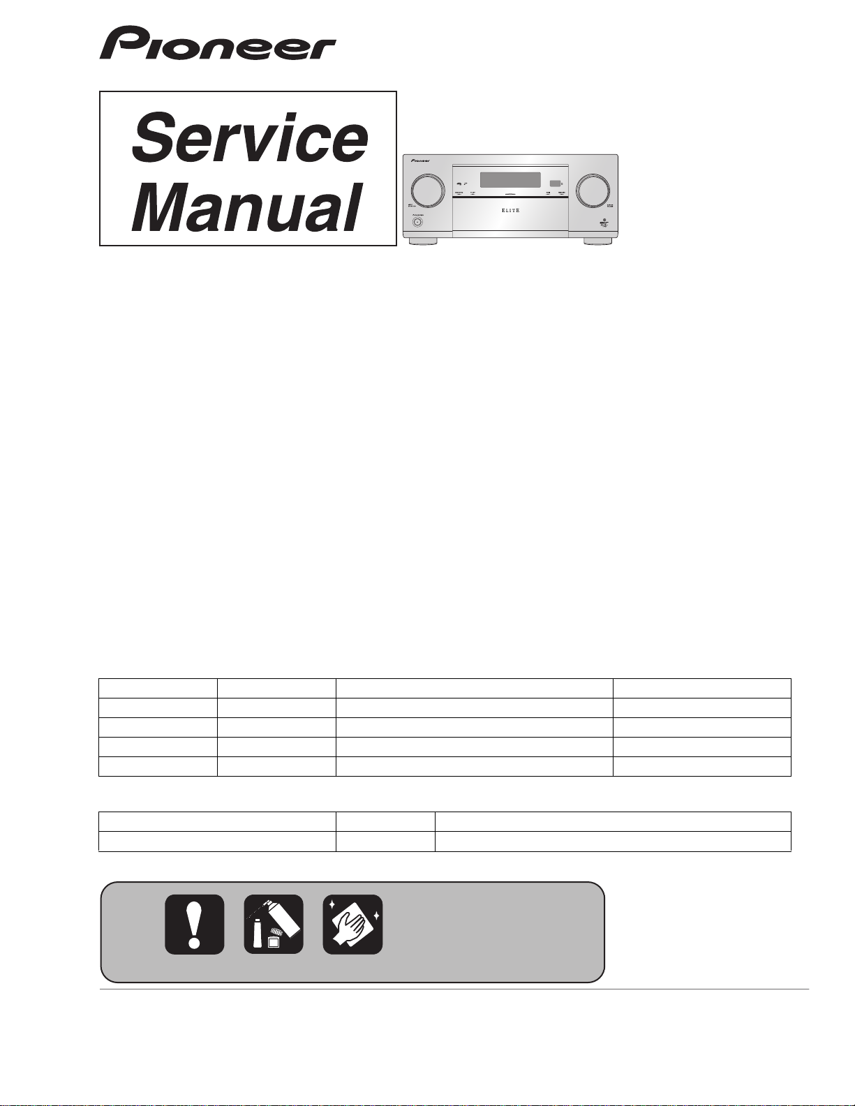
AV RECEIVER
SC-99
SC-97
SC-LX89-K
SC-LX89-S
SC-LX79-K
ORDER NO .
RRV4617
SC-99
SC-LX79-S
THIS MANUAL IS APPLICABLE TO THE FOLLOWING MODEL(S) AND TYPE(S).
Model Type Power Requirement Remarks
SC-99 CUXJ AC 120V
SC-97 CUXJ AC 120V
SC-LX89-K/-SSYXJ8 AC 220V to 230V
SC-LX79-K/-SSYXJ8 AC 220V to 230V
THIS SERVICE MANUAL SHOULD BE USED TOGETHER WITH THE FOLLOWING MANUAL(S).
Model No. Order No. Remarks
SC-99, SC-97, SC-LX89-K/-S,
SC-LX79-K/-S
ARP4004 SCHEMATIC DIAGRAM, PCB CONNECTION DIAGRAM
K-FZV OCT.
2015 Printed in Japan
Page 2
1
1. SAFETY PRECAUTIONS
The following check should be performed for the
continued protection of the customer and service
technician.
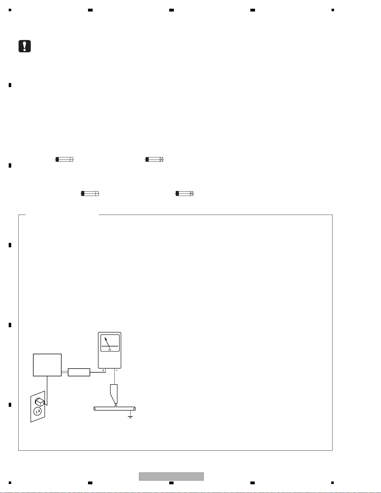
LEAKAGE CURRENT CHECK
Measure leakage current to a known earth ground
(water pipe, conduit, etc.) by connecting a leakage
current tester such as Simpson Model 229-2 or
equivalent between the earth ground and all exposed
metal parts of the appliance (input/output terminals,
screwheads, metal overlays, control shaft, etc.). Plug
the AC line cord of the appliance directly into a 120V
AC 60 Hz outlet and turn the AC power switch on. Any
current measured must not exceed 0.5 mA.
ANY MEASUREMENTS NOT WITHIN THE LIMITS
OUTLINED ABOVE ARE INDICATIVE OF A POTENTIAL
SHOCK HAZARD AND MUST BE CORRECTED BEFORE
RETURNING THE APPLIANCE TO THE CUSTOMER.
2. PRODUCT SAFETY NOTICE
Many electrical and mechanical parts in the appliance
have special safety related characteristics. These are
often not evident from visual inspection nor the protection
afforded by them necessarily can be obtained by using
replacement components rated for voltage, wattage, etc.
Replacement parts which have these special safety
characteristics are identified in this Service Manual.
Electrical components having such features are
identified by marking with a > on the schematics and on
the parts list in this Service Manual.
The use of a substitute replacement component which
does not have the same safety characteristics as the
PIONEER recommended replacement one, shown in the
parts list in this Service Manual, may create shock, fire,
or other hazards.
Product Safety is continuously under review and new
instructions are issued from time to time. For the latest
information, always consult the current PIONEER Service
Manual. A subscription to, or additional copies of,
PIONEER Service Manual may be obtained at a nominal
charge from PIONEER.
Leakage
current
tester
Reading should
not be above
0.5 mA
Device
under
test
Test all
exposed metal
surfaces
Also test with
plug reversed
(Using AC adapter
plug as required)
Earth
ground
AC Leakage Test
(FOR USA MODEL ONLY)
WARNING
This product contains lead in solder and certain electrical parts contain chemicals which are known to the state of California to
cause cancer, birth defects or other reproductive harm.
56 noitisoporP - 6.94252 noitceS edoC ytefaS & htlaeH
NOTICE
(FOR CANADIAN MODEL ONLY)
Fuse symbols (fast operating fuse) and/or (slow operating fuse) on PCB indicate that replacement parts must
be of identical designation.
REMARQUE
(POUR MODÈLE CANADIEN SEULEMENT)
Les symboles de fusible (fusible de type rapide) et/ou (fusible de type lent) sur CCI indiquent que les pièces
de remplacement doivent avoir la même désignation.
This service manual is intended for qualified service technicians ; it is not meant for the casual do-ityourselfer. Qualified technicians have the necessary test equipment and tools, and have been trained
to properly and safely repair complex products such as those covered by this manual.
Improperly performed repairs can adversely affect the safety and reliability of the product and may
void the warranty. If you are not qualified to perform the repair of this product properly and safely, you
should not risk trying to do so and refer the repair to a qualified service technician.
2 3 4
SAFETY INFORMATION
A
B
C
D
E
F
2
1
2 3 4
SC-99
Page 3

5
6 7 8
CONTENTS
SAFETY INFORMATION............................................................................................. .............................................................2
1. SERVICE PRECAUTIONS....................................................................................................................................................4
1.1 NOTES ON SOLDERING...............................................................................................................................................4
1.2 NOTES ON REPLACING ...............................................................................................................................................4
1.3 CAUTION................................... .. .......................................... .........................................................................................4
1.4 NOTES ON ASSEMBLING.............................................................................................................................................5
2. SPECIFICATIONS.................................................................................................................................................................6
2.1 SC-99, SC-97 SPECIFICATIONS...................................................................................................................................6
2.2 SC-LX89, SC-LX79 SPECIFICATIONS..........................................................................................................................8
3. BASIC ITEMS FOR SERVICE............................................................................................................................................10
3.1 CHECK POINTS AFTER SERVICING .........................................................................................................................10
3.2 PCB LOCATIONS.........................................................................................................................................................11
3.3 JIGS LIST.....................................................................................................................................................................14
4. BLOCK DIAGRAM..............................................................................................................................................................15
4.1 OVERALL WIRING DIAGRAM ...................................................................................... ...............................................15
4.2 BLOCK DIAGRAM FOR AUDIO BLOCK......................................................................................................................16
4.3 BLOCK DIAGRAM FOR DIGITAL MAIN VIDEO BLOCK .............................................................................................17
4.4 BLOCK DIAGRAM FOR DIGITAL MAIN AUDIO BLOCK .............................................................................................18
5 BLOCK DIAGRAM FOR VIDEO BLOCK......................................................................................................................19
4.
4.6 BLOCK DIAGRAM FOR POWER BLOCK (1)..............................................................................................................20
4.7 BLOCK DIAGRAM FOR POWER BLOCK (2)..............................................................................................................21
5. DIAGNOSIS ........................................................................................................................................................................22
5.1 DIAGNOSIS FLOWCHART..........................................................................................................................................22
5.2 CIRCUIT DESCRIPTION..............................................................................................................................................33
5.3 CONFIRMATION OF THE NETWORK MODULE.........................................................................................................42
6. SERVICE MODE.................................................................................................................................................................44
7. DISASSEMBLY ...................................................................................................................................................................47
8. EACH SETTING AND ADJUSTMENT................................................................................................................................68
8.1 ADJUSTMENT REQUIRED WHEN THE UNIT IS REPAIRED OR REPLACED..........................................................68
8.2 HOW TO SAVE AND LOAD THE SETTING USING BACKUP FUNCTION WITH USB MEMORY..............................69
8.3 REGION WRITING....................................... ... .......................................... ...................................................................70
8.4 HOW TO UPDATE FIRMWARE....................................................................................... .............................................71
9. EXPLODED VIEWS AND PARTS LIST...............................................................................................................................74
9.1 PACKING SECTION.....................................................................................................................................................74
9.2 EXTERIOR SECTION ..................................................................................................................................................76
9.3 REAR SECTION...........................................................................................................................................................78
...................80
9.4 CHASSIS SECTION............................................................................................................................
9.5 FRONT SECTION ........................................................................................................................................................82
10. PCB PARTS LIST..............................................................................................................................................................84
......
A
B
C
D
E
F
SC-99
5
6 7 8
3
Page 4
1
• For environmental protection, lead-free solder is used on the printed circuit boards mounted in this unit.
Be sure to use lead-free solder and a soldering iron that can meet specifications for use with lead-free solders for repairs
accompanied by reworking of soldering.
Do NOT use a soldering iron whose tip temperature cannot be controlled.
The part listed below is difficult to replace as a discrete component part.
When the part listed in the table is defective, replace whole Assy.
ASSY NAME
PCB ASSY
Part No.
Ref No. FUNCTION Part No. Remarks
IC451 3CH SW POWER SUPPLY IC TPS65251RHA-TLB
IC with heat-pad
IC1204 VIDEO PROCESSOR IC 88DE2750-K
IC1212 DDR IC K4T51163QJ-BCE7-K
IC BGA type
IC1602 HDMI INTERFACE IC MN864787-K
IC1609 HDMI INTERFACE IC MN864788-K
IC9002 DSP IC CS49844A-K
IC with heat-pad
IC9206 APPLE AUTHENTICATION IC H337S3959-TBB
IC9602 HDMI SW IC SII9589CTUC-3-K
MM3543BH-TBB
IC9403
IC9514
IC9515
POWER SUPPLY IC
MIC94325YMT-TBB
IC9523
IC9703 DSP IC D808K013DPTP456-K
IC with heat-pad
JA1601
JA1602
JA1603
HDMI Connector AKP7268-A-K JACK with Cu-through-hole & SMD type
JA9202 LAN Connector AKN7115-A JACK with Cu-through-hole & 10 pin
JA9601
JA9602
JA9603
JA9604
JA9605
JA9606
JA9607
DIGITAL
MAIN
ASSY
AWX2013
(SC-99)
AWX2017
(SC-97)
AWX2014
(SC-LX89)
AWX2018
(SC-LX79)
JA9620
HDMI Connector
AKP7268-A-K JACK with Cu-through-hole & SMD type
Q4101
Q4102
Q4201
Q4202
Q4301
Q4302
Q4401
Q4402
Q4501
Q4502
Q4601
Q4602
Q4701
Q4702
Q4801
Q4802
Q4901
D AMP
ASSY
AWH7104
(SC-99)
AWH7108
(SC-97)
AWH7105
(SC-LX89)
AWH7109
(SC-LX79)
Q4902
FET IRF6775MPBFS1-TRB Pins are under the parts side.
DISPLAY
ASSY
AWX2026
(SC-99,SC-97)
AWX2027
(SC-LX89,
SC-LX79)
IC6001 FLASH BLANK UC IC R5F100MHAFA-K Software is not written.
• Discharging
Before starting the diagnosis, wait for three minutes until the electricity of the unit is discharged.
• Ground Points
Please refer to “Ground Points”.
2 3 4
1. SERVICE PRECAUTIONS
1.1 NOTES ON SOLDERING
A
1.2 NOTES ON REPLACING
B
4
1
2 3 4
SC-99
C
D
E
1.3 CAUTION
F
Page 5
5
D AMP ASSY
Rear Panel
IR BUFFER_M ASSY
Accessory of Panel Base
IR Cover 85 (MTL)
BUFFER GND_M ASSY
BIND DM CABLE_M ASSY
Note : The right and left positions for the attachment positioning of digital amplifier block are gradual, however, adjust the
front and back positions correctly. For the positioning procedure, refer to "7. DISASSEMBLY".
When assembling the digital amplifier block, please note the following points of screws to prevent from short-circuit.
The following 7 points of screws must always be used AMZ30P060FTC
Points to be watched for swarf
If a screw at any of these points needs to be removed for service,
be sure to check that the swarf is not on the screw before refastening.
6 7 8
1.4 NOTES ON ASSEMBLING
A
B
C
D
E
5
6 7 8
SC-99
F
5
Page 6

1
Amplifier section
Continuous average power output*
8 Ω ................................................................................................................................... 140 W** per channel
6 Ω ...................................................................................... 200 W (SC-99)*** / 190 W (SC-97)*** per channel
* Measured pursuant to the Federal Trade Commission’s Trade Regulation rule on Power Output Claims for
Amplifiers
** 1 kHz with no more than 0.08 %**** total harmonic distortion
*** 1 kHz with no more than 1 %**** total harmonic distortion
**** Measured by Audio Spectrum Analyzer
Multi channel simultaneous power output (1 kHz, 1 %, 8 Ω)
9 ch total.............................................................................................................850 W (SC-99)/810 W (SC-97)
Continuous Power Output (1 kHz, 8 Ω, 0.08 %)
Front...........................................................................................................................................140 W + 140 W
Center...................................................................................................................................................... 140 W
Surround....................................................................................................................................140 W + 140 W
Surround back............................................................................................................................140 W + 140 W
Top middle/Extra 1......................................................................................................................140 W + 140 W
Continuous Power Output (1 kHz, 6 Ω, 1.0 %)
Front...................................................................................... 200 W + 200 W (SC-99)/190 W + 190 W (SC-97)
Center................................................................................................................ 200 W (SC-99)/190 W (SC-97)
Surround............................................................................... 200 W + 200 W (SC-99)/190 W + 190 W (SC-97)
Surround back....................................................................... 200 W + 200 W (SC-99)/190 W + 190 W (SC-97)
Top middle/Extra 1................................................................. 200 W + 200 W (SC-99)/190 W + 190 W (SC-97)
Continuous Power Output (1 kHz, 4 Ω, 1.0 %)
Front...................................................................................... 255 W + 255 W (SC-99)/240 W + 240 W (SC-97)
Center................................................................................................................ 255 W (SC-99)/240 W (SC-97)
Surround............................................................................... 255 W + 255 W (SC-99)/240 W + 240 W (SC-97)
Surround back....................................................................... 255 W + 255 W (SC-99)/240 W + 240 W (SC-97)
Top middle/Extra 1................................................................. 255 W + 255 W (SC-99)/240 W + 240 W (SC-97)
Total harmonic distortion................................................................................ 0.04 % (1 kHz, 130 W + 130 W, 8 Ω)
Guaranteed speaker impedance........................................................................................................... 4 Ω to 16 Ω
Audio Section
Input (Sensitivity/Impedance)
PHONO MM................................................................................................................................... 5 mV/47 k Ω
LINE........................................................................................................................................... 400 mV/47 kΩ
Output (Level/Impedance)
REC........................................................................................................................................... 400 mV/2.2 kΩ
Signal-to-Noise Ratio (IHF, short circuited, A network)
LINE........................................................................................................................................................103 dB
Tuner Section
Frequency Range (FM)..........................................................................................................87.5 MHz to 108 MHz
Antenna Input (FM)...................................................................................................................... 75 Ω unbalanced
Frequency Range (AM).......................................................................................................... 530 kHz to 1 700 kHz
Antenna (AM).................................................................................................................. Loop antenna (balanced)
Video Section
Signal level
Composite Video...........................................................................................................................1 Vp-p (75 Ω)
Component Video...........................................................................Y: 1.0 Vp-p (75 Ω ), PB/PR: 0.7 Vp-p (75 Ω)
Corresponding maximum resolution
Component Video..........................................................................................................................1080i (1125i)
Digital In/Out Section
Bluetooth Section
HDMI terminal.................................................................................................................................19-pin (Not DVI)
HDMI output type....................................................................................................................................5 V, 55 mA
HDMI input/MHL terminal..................................................................................................................... 5 V, 900 mA
USB terminal.................................................................................................USB2.0 High Speed (Type A) 5 V, 1 A
USB terminal (SC-99 only).........................................................................................USB2.0 High Speed (Type B)
iPod terminal.....................................................................................................................................................USB
Version
Output
Estimated line-of-sight transmission distance*
*The line-of-sight transmission distance is an estimate. Actual transmission distances supported may differ
depending on surrounding conditions.
Frequency range
Supported Bluetooth profiles
Supported Codec
........................................................................................................
......................................................................................................................
........................................................................................
.........................................................................................................................................
.............................................................................................................
........................................................................................................
Bluetooth Specification Ver. 2.1 + EDR
Bluetooth Specification Class 2
About 10 m
2.4 GHz
A2DP, AVRCP
SBC (Subband Codec), AAC
2 3 4
2. SPECIFICATIONS
2.1 SC-99, SC-97 SPECIFICATIONS
A
B
C
D
E
F
6
1
2 3 4
SC-99
Page 7

5
Digital In/Out Section
HDMI terminal ................................................................................................................................19-pin (Not DVI)
HDMI output type ....................................................................................................................................5 V, 55 mA
HDMI input/MHL terminal ....................................................................................................................5 V, 900 mA
USB terminal ................................................................................................USB2.0 High Speed (Type A) 5 V, 1 A
USB terminal (SC-99 only)...........................................................................................USB2.0 High Speed (Type B)
iPod terminal .................................................................................................................................................... USB
Integrated Control Section
Control (IR) terminal .............................................................................................................ø 3.5 Mini-jack (MONO)
IR signal ...................................................................................................................High Active (High Level: 2.0 V)
12 V Trigger terminal........................................................................................................... ø 3.5 Mini-jack (MONO)
12 V Trigger output type...............................................................................................................12 V, Total 150 mA
RS-232C cable type................................................................................................9-pin, cross type, female-female
Network Section (Wired)
LAN terminal.....................................................................................................................10 BASE-T/100 BASE-TX
Network Section (Wireless)
WLAN standards..........................................................IEEE 802.11a, IEEE 802.11b, IEEE 802.11g, IEEE 802.11n
Frequency band
2.4GHz band (2.412GHz to 2.462GHz)......................................................................Channel1 to Channel11
5GHz band (5.180GHz to 5.240GHz, 5.745GHz to 5.825GHz)
.....................................................................................Channel36 to Channel48, Channel149 to Channel165
Security ..............................................................................................................................Disabled (no encryption)
WEP (Key length: 64 bit/128 bit, Key format: ASCII/Hex)
WPA2 Mixed (WPA/WPA2, Encryption method: TKIP/AES, Recognition method: PSK)
Miscellaneous
Power requirements.........................................................................................................................AC 120 V, 60 Hz
Power consumption.........................................................................................................................................370 W
In standby..................................................................................................................................................0.1 W
In standby (HDMI control on).....................................................................................................................0.3 W
In standby (Network standby on)............................................................................................................... 2.7 W
In standby (Network standby on, wireless LAN connected)........................................................................3.0 W
In standby (HDMI control on, Network standby on)....................................................................................2.7 W
In standby (HDMI control on, Network standby on, wireless LAN connected)............................................3.0 W
Auto power down................................................................................................15 min, 30 min, 60 min, off (default)
Dimensions............................................................................................... 435 mm (W) x 185 mm (H) x 441 mm (D)
(17.13 in. (W) x 7.28 in. (H) x 17.36 in. (D))
Weight (without package)
SC-99.........................................................................................................................................17.6 kg (38.8 lb)
SC-97.........................................................................................................................................17.5 kg (38.6 lb)
Number of Furnished Parts
MCACC Setup microphone.......................................................................................................................................1
Remote control unit..................................................................................................................................................1
AAA size IEC R03 dry cell batteries...........................................................................................................................2
AM loop antenna.......................................................................................................................................................1
FM wire antenna.......................................................................................................................................................1
Power cord
CD-ROM
Quick start guide
Safety Brochure
Warranty sheet
For DTS patents, see http://patents.dts.com. Manufactured under license from DTS Licensing Limited. DTS, DTS-HD,
the Symbol, & DTS and the Symbol together are registered trademarks, and DTS-HD Master Audio and DTS Neo:X |
11.1 are a trademark of DTS, Inc. © DTS, Inc. All Rights Reserved.
Notes
Specifications and the design are subject to possible modifications without notice, due to improvements.
Windows® and the Windows logo are trademarks of the Microsoft group of companies.
Corporation and product names mentioned herein are trademarks or registered trademarks of the respective corporations.
The Wi-Fi CERTIFIED Logo is a certification mark of Wi-Fi Alliance.
The Wi-Fi Protected Setup Identifier Mark is a certification mark of Wi-Fi Alliance.
SABRE DAC
TM
and the logo are trademarks of ESS Technology, Inc.
HTC, HTC Connect and the HTC Connect logo are trademarks of HTC Corporation.
MHL, the MHL Logo, and Mobile High-Definition Link are trademarks or registered trademarks of MHL, LLC in the
United States and other countries.
Apple, AirPlay, iPad, iPhone, iPod, iPod nano, iPod touch, iTunes, Safari, Bonjour, Mac, Mac OS and OS X are trademarks
of Apple Inc., registered in the U.S. and other countries.
The AirPlay logo is a trademark of Apple Inc.
Manufactured under license from Dolby Laboratories. Dolby, Dolby Atmos, Dolby Surround, and the double-D symbol are trademarks of Dolby Laboratories.
6 7 8
A
B
C
D
E
5
SC-99
6 7 8
F
7
Page 8

1
Amplifier section
Multi channel simultaneous power output (1 kHz, 1 %, 8 Ω)
9 ch total.................................................................................................... 850 W (SC-LX89)/810 W (SC-LX79)
Rated power output (1 kHz, 4 Ω, 1 %, 1 ch Driven)........................260 W (SC-LX89)/250 W (SC-LX79) per channel
Rated power output (1 kHz, 6 Ω, 1 %, 1 ch Driven)........................220 W (SC-LX89)/210 W (SC-LX79) per channel
For Oceania model: Maximum power output (1 kHz, 4 Ω, 10 %, 1 ch Driven)
......................................................................................................370 W (SC-LX89)/350 W (SC-LX79) per channel
Total harmonic distortion.................................................................................0.04 % (1 kHz, 130 W + 130 W, 8 Ω)
Guaranteed speaker impedance...............................................................................................................4 Ω to 16 Ω
Audio Section
Input (Sensitivity/Impedance)
PHONO MM.....................................................................................................................................5 mV/47 kΩ
LINE.............................................................................................................................................400 mV/47 kΩ
Output (Level/Impedance)
REC.............................................................................................................................................400 mV/2.2 kΩ
Signal-to-Noise Ratio (IHF, short circuited, A network)
LINE.........................................................................................................................................................103 dB
Tuner Section
Frequency Range (FM)............................................................................................................87.5 MHz to 108 MHz
Antenna Input (FM).........................................................................................................................75 Ω unbalanced
Frequency Range (AM)............................................................................................................531 kHz to 1 602 kHz
Antenna (AM).....................................................................................................................Loop antenna (balanced)
Video Section
Signal level
Composite Video............................................................................................................................ 1 Vp-p (75 Ω)
Component Video............................................................................Y: 1.0 Vp-p (75 Ω), PB/PR: 0.7 Vp-p (75 Ω)
Corresponding maximum resolution
Component Video...........................................................................................................................1080i (1125i)
Bluetooth Section
Version..........................................................................................................Bluetooth Specification Ver. 2.1 + EDR
Output .......................................................................................................................Bluetooth Specification Class 2
Estimated line-of-sight transmission distance* ........................................................................................About 10 m
*The line-of-sight transmission distance is an estimate. Actual transmission distances supported may differ
depending on surrounding conditions.
Frequency range...........................................................................................................................................2.4 GHz
Supported Bluetooth profiles..............................................................................................................A2DP, AVRCP
Supported Codec..........................................................................................................SBC (Subband Codec), AAC
Digital In/Out Section
HDMI terminal..................................................................................................................................19-pin (Not DVI)
HDMI output type..................................................................................................................................... 5 V, 55 mA
HDMI input/MHL terminal ......................................................................................................................5 V, 900 mA
USB terminal..................................................................................................USB2.0 High Speed (Type A) 5 V, 1 A
USB terminal (SC-LX89 only)......................................................................................USB2.0 High Speed (Type B)
iPod terminal.......................................................................................................................................................USB
Integrated Control Section
Control (IR) terminal.............................................................................................................ø 3.5 Mini-jack (MONO)
IR signal.....................................................................................................................High Active (High Level: 2.0 V)
12 V Trigger terminal............................................................................................................ø 3.5 Mini-jack (MONO)
12 V Trigger output type...............................................................................................................12 V, Total 150 mA
RS-232C cable type .................................................................................................9-pin, cross type, female-female
Network Section (Wired)
LAN terminal.....................................................................................................................10 BASE-T/100 BASE-TX
Network Section (Wireless)
WLAN standards...........................................................IEEE 802.11a, IEEE 802.11b, IEEE 802.11g, IEEE 802.11n
Frequency band
2.4GHz band (2.412GHz to 2.472GHz).......................................................................Channel 1 to Channel 13
5GHz band (5.180GHz to 5.240GHz)........................................................................Channel 36 to Channel 48
Security...............................................................................................................................Disabled (no encryption)
WEP (Key length: 64 bit/128 bit, Key format: ASCII/Hex)
WPA2 Mixed (WPA/WPA2, Encryption method: TKIP/AES, Recognition method: PSK)
2 3 4
2.2 SC-LX89, SC-LX79 SPECIFICATIONS
A
B
C
D
E
F
8
1
2 3 4
SC-99
Page 9

5
Miscellaneous
Power requirements................................................................................................AC 220 V to 230 V, 50 Hz/60 Hz
Power consumption.........................................................................................................................................370 W
In standby...................................................................................................................................................0.1 W
In standby (HDMI control on).....................................................................................................................0.3 W
In standby (Network standby on)................................................................................................................2.7 W
In standby (Network standby on, wireless LAN connected)........................................................................3.0 W
In standby (HDMI control on, Network standby on)....................................................................................2.7 W
In standby (HDMI control on, Network standby on, wireless LAN connected).............................................3.0 W
Auto power down................................................................................................15 min (default), 30 min, 60 min, off
Dimensions................................................................................................435 mm (W) x 185 mm (H) x 441 mm (D)
Weight (without package)
SC-LX89..................................................................................................................................................18.1 kg
SC-LX79..................................................................................................................................................17.7 kg
Number of Furnished Parts
MCACC Setup microphone.......................................................................................................................................1
Remote control unit..................................................................................................................................................1
AAA size IEC R03 dry cell batteries.........................................................................................................................2
AM loop antenna.......................................................................................................................................................1
FM wire antenna.......................................................................................................................................................1
Wireless antenna.....................................................................................................................................................2
Power cord
CD-ROM
Quick start guide
Safety Brochure
Warranty sheet
For DTS patents, see http://patents.dts.com. Manufactured under license from DTS Licensing Limited. DTS, DTS-HD,
the Symbol, & DTS and the Symbol together are registered trademarks, and DTS-HD Master Audio and DTS Neo:X |
11.1 are a trademark of DTS, Inc. © DTS, Inc. All Rights Reserved.
Notes
Specifications and the design are subject to possible modifications without notice, due to improvements.
Windows® and the Windows logo are trademarks of the Microsoft group of companies.
Corporation and product names mentioned herein are trademarks or registered trademarks of the respective corporations.
The Wi-Fi CERTIFIED Logo is a certification mark of Wi-Fi Alliance.
The Wi-Fi Protected Setup Identifier Mark is a certification mark of Wi-Fi Alliance.
SABRE DAC
TM
and the logo are trademarks of ESS Technology, Inc.
HTC, HTC Connect and the HTC Connect logo are trademarks of HTC Corporation.
MHL, the MHL Logo, and Mobile High-Definition Link are trademarks or registered trademarks of MHL, LLC in the
United States and other countries.
Apple, AirPlay, iPad, iPhone, iPod, iPod nano, iPod touch, iTunes, Safari, Bonjour, Mac, Mac OS and OS X are trademarks
of Apple Inc., registered in the U.S. and other countries.
The AirPlay logo is a trademark of Apple Inc.
Manufactured under license from Dolby Laboratories. Dolby, Dolby Atmos, Dolby Surround, and the double-D symbol are trademarks of Dolby Laboratories.
6 7 8
A
B
5
SC-99
6 7 8
C
D
E
F
9
Page 10
1
10 Check the appearance of the product.
No scratches or dirt on its appearance after receiving it for service.
1 Check the firmware version. The firmware version must be the latest one.
If it is not the latest one, be sure to update it.
2 Confirm whether the customer complain has been solved.
If the customer complain occurs with the particular source, such
as Dolby Digital, DTS, AAC and HDMI, input it for the operation
check.
The customer complain must not be reappeared.
Video, Audio and operations must be normal.
5 Check a supported music file playback (e.g. wav. flac. mp3, etc).
(Make the connections with a USB memory or an iOS device)
Audio and operations including OSD output must be normal.
6 Check the surround playback.
(Select Surround mode and check the multichannel operations
via the DSP circuit.)
Each channel audio and operations must be normal.
3 Check the analog audio playback.
(Make the analog connections with a CD/DVD/BD player.)
Each channel audio and operations must be normal.
7 Check the video outputs.
(Connect with a BD player.)
Video and operations must be normal.
8 Check the tuner (AM and FM) operations. Audio and operations must be normal.
9 Check the sound from headphone output. Sound must be normal, without noise.
4 Check the HDMI digital audio playback.
(Make the digital connections with a BD player.)
Each channel audio and operations must be normal.
No. Procedures Check points
Items to be checked after servicing
To keep the product quality after servicing, confirm recommended check points shown below.
oidua gnidrager dekcehc eb ot metIoediv gnidrager dekcehc eb ot metI
Block noise Distortion
Horizontal noise Noise
Flicker Volume too low
Disturbed image (video jumpiness) Volume too high
Too dark Volume fluctuating
detpurretni dnuoSthgirb ooT
Mottled color
See the table below for the items to be checked regarding video and audio.
2 3 4
3. BASIC ITEMS FOR SERVICE
3.1 CHECK POINTS AFTER SERVICING
A
B
C
D
E
F
10
1
2 3 4
SC-99
Page 11
5
FFC GUARD_M ASSY
AN
SC-99/CUXJ,
SC-LX89-K/SYXJ8,
SC-LX89-S/SYXJ8 only
:USB DAC ASSY
SC-97/CUXJ,
SC-LX79-K/SYXJ8,
SC-LX79-S/SYXJ8 only
:PRIMARY SHIELD
ASSY
U
E
COMPOSITE ASSY
J
USB RECT_M ASSY
D
INTERFACE_M ASSY
H
AUDIO ASSY
A
COMPONENT ASSY
I
B DIODE ASSY
X
DIGITAL MAIN ASSY
G
Network Module
VREG GUARD ASSY
AO
BIND B CABLE ASSY
AM
DAC HIGH ASSY
B
BUFFER GND_M ASSY
Q
IR REG_M ASSY
W
PRE BRIDGE_M ASSY
AA
A-DAC BRIDGE ASSY
AB
D-AUDIO BRIDGE ASSY
AC
CONNECT_M ASSY
Y
F
FB CONNECT ASSY
Z
AD
D-DAC BRIDGE
ASSY
FRONT BRIDGE
ASSY
AE
AF
DISPLAY BRIDGE
ASSY
AG
F-IN BRIDGE ASSY
FAN CONNECT ASSY
AK
AJ
MIC HP GUARD ASSY
AI
A REG BRIDGE ASSY
AL
PRIMARY ASSY
BIND DM CABLE_M
ASSY
T
V
REG ASSY
IR BUFFER_M ASSY
P
D AMP ASSY
S
IR INTERFACE_M
ASSY
R
AH
SC-99/CUXJ,
SC-LX89-K/SYXJ8,
SC-LX89-S/SYXJ8 only
:MCH BRIDGE ASSY
SC-99/CUXJ,
SC-LX89-K/SYXJ8,
SC-LX89-S/SYXJ8 only
:MULTI CH IN ASSY
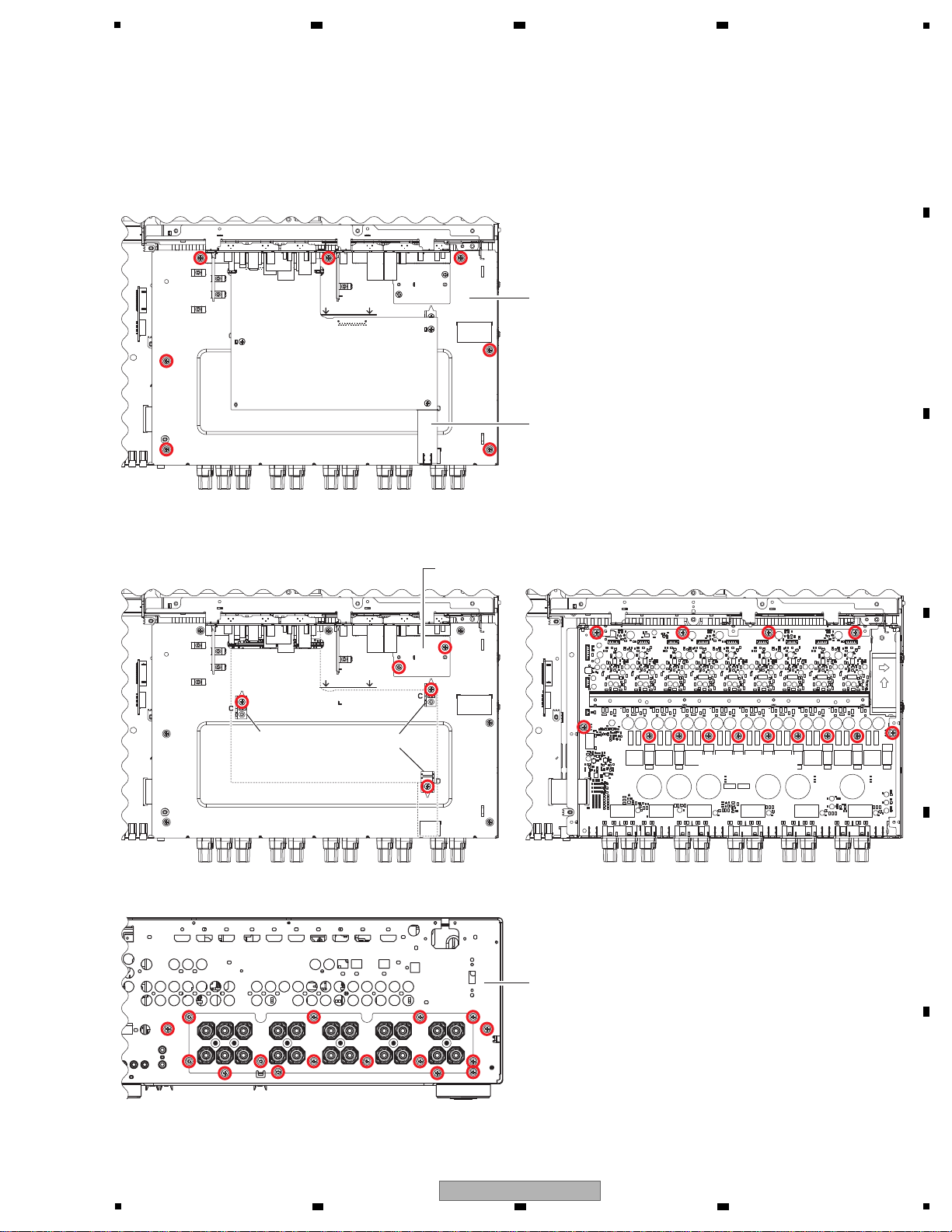
3.2 PCB LOCATIONS
6 7 8
A
B
C
D
E
F
SC-99
5
6 7 8
11
Page 12
1
VOL ASSY
ENCODER ASSY
DISPLAY ASSY
POWER SW ASSY
FRONT HDMI USB
ASSY
C
PANEL GUARD
ASSY
MIC HP ASSY
K
M
AP
O
L
N
NOTES: - Parts marked by “NSP” are generally unavailable because they are not in our Master Spare Parts List.
-
The > mark found on some component parts indicates the importance of the safety factor of the part.
Therefore, when replacing, be sure to use parts of identical designation.
A
B
2 3 4
Mark No. Description Part No.
LIST OF ASSEMBLIES
1...D AMP ASSY (SC-99) AWH7104
1...D AMP ASSY (SC-97) AWH7108
1...D AMP ASSY (SC-LX89) AWH7105
1...D AMP ASSY (SC-LX79) AWH7109
C
NSP 1...AUDIO COMPOSITE_H ASSY (SC-99) AWR7288
2..AUDIO ASSY AWX2076
2..COMPOSITE ASSY AWX2085
2..D-AUDIO BRIDGE ASSY AWX2196
2..D-DAC BRIDGE ASSY AWX2197
2..A-DAC BRIDGE ASSY AWX2198
NSP 1...AUDIO COMPOSITE_H ASSY (SC-97) AWR7292
2..AUDIO ASSY AWX2080
2..COMPOSITE ASSY AWX2086
2..D-AUDIO BRIDGE ASSY AWX2196
2..D-DAC BRIDGE ASSY AWX2197
2..A-DAC BRIDGE ASSY AWX2198
NSP 1...AUDIO COMPOSITE_H ASSY (SC-LX89) AWR7289
D
E
2..AUDIO ASSY AWX2077
2..COMPOSITE ASSY AWX2085
2..D-AUDIO BRIDGE ASSY AWX2196
2..D-DAC BRIDGE ASSY AWX2197
2..A-DAC BRIDGE ASSY AWX2198
NSP 1...AUDIO COMPOSITE_H ASSY (SC-LX79) AWR7293
2..AUDIO ASSY AWX2081
2..COMPOSITE ASSY AWX2086
2..D-AUDIO BRIDGE ASSY AWX2196
2..D-DAC BRIDGE ASSY AWX2197
2..A-DAC BRIDGE ASSY AWX2198
NSP 1...PRIM DISPLAY ASSY (SC-99/SC-97) AWM8417
2..MIC HP ASSY AWX2048
2..DISPLAY ASSY AWX2026
2..VOL ASSY AWX2029
2..POWER SW ASSY AWX2030
2..PRIMARY ASSY AWX2038
2..ENCODER ASSY AWX2051
2..MIC HP GUARD ASSY AWX2052
2..FAN CONNECT ASSY AWX2055
NSP 2..VREG GUARD ASSY AWX2053
NSP 2..PANEL GUARD ASSY AWX2054
Mark No. Description Part No.
NSP 1...PRIM DISPLAY ASSY (SC-LX89/SC-LX79) AWM8418
2..MIC HP ASSY AWX2049
2..DISPLAY ASSY AWX2027
2..VOL ASSY AWX2029
2..POWER SW ASSY AWX2030
2..PRIMARY ASSY AWX2039
2..ENCODER ASSY AWX2051
2..MIC HP GUARD ASSY AWX2052
2..FAN CONNECT ASSY AWX2055
NSP 2..VREG GUARD ASSY AWX2053
NSP 2..PANEL GUARD ASSY AWX2054
NSP 1...IR BUFFER_M ASSY (SC-99/SC-97) AWM8423
2..IR BUFFER_M ASSY AWX2093
2..BUFFER GND_M ASSY AWX1783
NSP 1...IR BUFFER_M ASSY (SC-LX89) AWM8424
2..IR BUFFER_M ASSY AWX2094
2..BUFFER GND_M ASSY AWX1783
NSP 1...IR BUFFER_M ASSY (SC-LX79) AWM8426
2..IR BUFFER_M_ASSY AWX2096
2..BUFFER GND_M ASSY AWX1783
NSP 1...INTERFACE REG_M ASSY (SC-99) AWR7296
2..INTERFACE_M ASSY AWX2120
2..IR REG_M ASSY AWX2124
2..B DIODE ASSY AWX2130
2..PRE BRIDGE_M ASSY AWX1822
2..A REG BRIDGE ASSY AWX2132
NSP 2..FFC GUARD_M ASSY AWX1821
NSP 2..BIND B CABLE ASSY AWX1826
NSP 1...INTERFACE REG_M ASSY (SC-97) AWR7299
2..INTERFACE_M ASSY AWX2120
2..IR REG_M ASSY AWX2127
2..B DIODE ASSY AWX2130
2..PRIMARY SHIELD ASSY AWX1820
2..PRE BRIDGE_M ASSY AWX1822
2..A REG BRIDGE ASSY AWX2132
NSP 2..FFC GUARD_M ASSY AWX1821
NSP 2..BIND B CABLE ASSY AWX1826
NSP 1...INTERFACE REG_M ASSY (SC-LX89) AWR7297
2..INTERFACE_M ASSY AWX2121
2..IR REG_M ASSY AWX2125
2..B DIODE ASSY AWX2131
2..PRE BRIDGE_M ASSY AWX1822
2..A REG BRIDGE ASSY AWX2133
NSP 2..FFC GUARD_M ASSY AWX1821
NSP 2..BIND B CABLE ASSY AWX1826
F
12
1
2 3 4
SC-99
Page 13

5
6 7 8
Mark No. Description Part No.
Mark No. Description Part No.
NSP 1...INTERFACE REG_M ASSY (SC-LX79) AWR7300
2..INTERFACE_M ASSY AWX2121
2..IR REG_M ASSY AWX2128
2..B DIODE ASSY AWX2131
2..PRIMARY SHIELD ASSY AWX1820
2..PRE BRIDGE_M ASSY AWX1822
2..A REG BRIDGE ASSY AWX2133
NSP 2..FFC GUARD_M ASSY AWX1821
NSP 2..BIND B CABLE ASSY AWX1826
NSP 1...REG BRIDGE ASSY (SC-99) AWR7306
2..REG ASSY AWX2149
2..FRONT BRIDGE ASSY AWX1833
2..DISPLAY BRIDGE ASSY AWX2155
2..F-IN BRIDGE ASSY AWX2158
2..MULTI CH IN ASSY AWX2159
2..MCH BRIDGE ASSY AWX1840
2..FB CONNECT ASSY AWX1841
2..CONNECT_M ASSY AWX2162
2..USB RECT_M ASSY AWX2165
2..BIND DM CABLE_M ASSY AWX1846
NSP 1...REG BRIDGE ASSY (SC-97) AWR7309
2..REG ASSY AWX2152
2..FRONT BRIDGE ASSY AWX1833
2..DISPLAY BRIDGE ASSY AWX2155
2..F-IN BRIDGE ASSY AWX2158
2..FB CONNECT ASSY AWX1841
2..CONNECT_M ASSY AWX2162
2..USB RECT_M ASSY AWX2165
2..BIND DM CABLE_M ASSY AWX1846
NSP 1...REG BRIDGE ASSY (SC-LX89) AWR7307
2..REG ASSY AWX2150
2..FRONT BRIDGE ASSY AWX1833
2..DISPLAY BRIDGE ASSY AWX2156
2..F-IN BRIDGE ASSY AWX2158
2..MULTI CH IN ASSY AWX2160
2..MCH BRIDGE ASSY AWX1840
2..FB CONNECT ASSY AWX1841
2..CONNECT_M ASSY AWX2163
2..USB RECT_M ASSY AWX2166
2..BIND DM CABLE_M ASSY AWX1846
1...DIGITAL MAIN ASSY (SC-99) AWX2013
2..NETWORK MODULE AXX7293
1...DIGITAL MAIN ASSY (SC-97) AWX2017
2..NETWORK MODULE AXX7293
1...DIGITAL MAIN ASSY (SC-LX89) AWX2014
2..NETWORK MODULE AXX7293
1...DIGITAL MAIN ASSY (SC-LX79) AWX2018
2..NETWORK MODULE AXX7293
1...FRONT HDMI USB ASSY (SC-99/SC-97) AWX2115
1...FRONT HDMI USB ASSY (SC-LX89) AWX2116
1...FRONT HDMI USB ASSY (SC-LX79) AWX2118
1...USB DAC ASSY (SC-99) AWX2056
1...USB DAC ASSY (SC-LX89) AWX2057
A
B
C
NSP 1...REG BRIDGE ASSY (SC-LX79) AWR7310
2..REG ASSY AWX2153
2..FRONT BRIDGE ASSY AWX1833
2..DISPLAY BRIDGE ASSY AWX2156
2..F-IN BRIDGE ASSY AWX2158
2..FB CONNECT ASSY AWX1841
2..CONNECT_M ASSY AWX2163
2..USB RECT_M ASSY AWX2166
2..BIND DM CABLE_M ASSY AWX1846
1...IR INTERFACE_M ASSY AWX1776
1...DAC HIGH ASSY (SC-99) AWX2063
1...DAC HIGH ASSY (SC-97) AWX2067
1...DAC HIGH ASSY (SC-LX89) AWX2064
1...DAC HIGH ASSY (SC-LX79) AWX2068
1...COMPONENT ASSY (SC-99) AWX2105
1...COMPONENT ASSY (SC-97) AWX2108
1...COMPONENT ASSY (SC-LX89) AWX2106
1...COMPONENT ASSY (SC-LX79) AWX2109
D
E
F
SC-99
5
6 7 8
13
Page 14
3.3 JIGS LIST
[1] Jigs List
Name
Jig No.
Remarks
Diagnosis for AUDIO ASSY, D AMP ASSY
Diagnosis for AUDIO ASSY, D AMP ASSY,
DIGITAL MAIN ASSY(side-B), DAC HIGH ASSY, USB DAC ASSY
Diagnosis for AUDIO ASSY, D AMP ASSY,
DIGITAL MAIN ASSY(side-B), DAC HIGH ASSY, USB DAC ASSY
Diagnosis for AUDIO ASSY, D AMP ASSY,
DIGITAL MAIN ASSY(side-B), DAC HIGH ASSY, USB DAC ASSY
Diagnosis for AUDIO ASSY, D AMP ASSY
Diagnosis for DIGITAL MAIN ASSY(side-B), DAC HIGH ASSY,
USB DAC ASSY
Diagnosis for DIGITAL MAIN ASSY(side-B), DAC HIGH ASSY,
USB DAC ASSY
Diagnosis for DIGITAL MAIN ASSY(side-B), DAC HIGH ASSY,
USB DAC ASSY
Diagnosis for DIGITAL MAIN ASSY(side-B), DAC HIGH ASSY,
USB DAC ASSY
15P FFC extension jig cable GGD1680
29P board to board extension jig cable GGD1856
5P board to board extension jig cable GGD1857
24P board to board extension jig cable x 2
GGD1871
5P PH Housing ASSY extension jig cable GGD1594
23P board to board extension jig cable GGD1875
30P + 30P board to board extension jig cable
GGD1682
28P board to board extension jig cable GGD1867
20P board to board extension jig cable GGD1868
[2] Lubricants and Glues List
Name
Lubricants and Glues No.
Remarks
Silicone Grease
GYA1001
Refer to “9.5 FRONT SECTION”
[3] Cleaning
Before shipping out the product, be sure to clean the following positions by using the prescribed cleaning tools.
Name skrameR.oN traPdenaelc eb ot noitisoP
Refer to “9.4 CHASSIS SECTION”Cleaning paper GED-008Fan
A
1
2 3 4
B
C
D
E
F
14
SC-99
1
2 3 4
Page 15
4. BLOCK DIAGRAM
24
20
23
20
15/60
9/65
TUNER
MODULE
24
24
3
!
AC CORD
SECONDARY
PRIMARY
3/100
*2mm
4/100
39/120
7
5
1.-B+15V
2.-B
1.V+12_DF
2.GND_DF
3.V-12_DF
4.GND_DF(S)
5.V+12_RY
6.V-12_RY
7.V+15_VDD
3
2
1.ACWP
2.GNDV
3.GNDV
4.V+5_V
5.-VF
6.FL AC2
7.FL AC1
15/330
FAN
B-DIODEIR REG
REG
REG
USB RECT
19.EXSO
18.EXSCK
17.EXOE
16.EXST
15.XOLERR
14.XBERR
13.IRMUTEA
12.IRMUTESB
11.IRMUTEFH
10.RY_FW
9.RY_AF
8.Ry_CR
7.Ry_FH
6.Ry_B
5.AMP_TEMP
4.XTEMPSD5
3.XDCERR
2.GNDD
1.GNDD
3.LOCKDET
2.V-FAN
1.V+FAN
19/90
4
*1.00mm
55 5555 5
!
FU32
!
FU31
!
FU21
!
FU22
1.V+8_MD
2.GND_MD
3.V-8_MD
4.GND_MD(S)
4
!
FU12!FU11
!
FU15
!
FU14!FU13
ADD7795-
ADD7791-
ADD7725-
ADD7794-
ADX7746-
4/195
ADD7796-
D20PYY0410E
D20PYY0310E
ADX7755-
4/375
ADX7759-
3/190
*1.00mm
!
4.-B
3.GND
2.GND
1.+B
CN8301
CN3472
CN6001
JP6004
JP6002
CN7006
CN4000
CN4001
JP3001
CN7723
CN2503
CN7724
CN3051
CN6952
CN3601
CN8303
JP7725
CN6801
CN6951
JP8402
CN7401
CN7400
CN7201
CN7251CN7241
CN7271
CN7281
CN7502
CN7603
CN6803 CN6802
CN3801CN3802
24 24
2424
*1
*4
*4
*4
!
*4
AXM7040-
*1 !
BOARD IN
FFC
2.0mm FLAT CABLE
FFC CONNECTOR
2.0mm CABLE HOLDER
*2mm
BOARD TO BOARD
CN4002
CN4003
CN4004
2
4
7
T1501
CAUTION - FOR CONTINUED PROTECTION AGAINST RISK OF FIRE,
REPLACE WITH SAME TYPE AND RATINGS OF FUSE.
4.-B(-65V)
3.GND
2.GND
1.+B(+65V)
*3
5 55555 5
CN3870
CN3880CN3890 CN3830
CN3840
CN3850
CN3860
CN4700
CN4100CN4200 CN4300CN4400CN4500CN4600
CN7601
CN7501
S2,S3,S9
S5,S6
S4
S1
S7
4
JP6001
CN6003
ADD7783-
5/60
8
24
ANOTHER CONNECTOR
CN3401
CN3371
J3004
J3002
JUMPER CONNECTOR
28
CN2502
20
CN3001
CN3902
18
CN251018CN7671
18
CN767218CN7761
CN7722
7 17
CN7721
2820
CN3794CN3792
2820
CN3793CN3791
3030
CN3783 CN3781
2820
30 30
13
CN7953CN7954
23
717
CN7684
CN7683
717
CN7682CN7681
717
CN7002 CN7007
13
CN7004 CN7003
7
CN7005
15
CN7008
157
CN7661CN7662
7
V-REG A-REG
1.XFANERR
2.FANCTLL
3.FANCTLH
4.EXSO
5.EXSCK
6.EXOE
7.EXST
8.XOLERR
9.AMP_TEMP
10.IRMUTEA
11.IRMUTESB
12.IRMUTEFH
13.RY_FW
1.XFANERR
2.FANCTLH
3.FANCTLL
4.XMICDET
5.V-7_A
6.GNDA
7.GNDA
8.V+7_A
9.MICOUT
10.GNDA
11.HPL
12.GNDHP
13.GNDHP
14.HPR
15.GNDHP
16.AMUTE
17.XHPDET
7.FLAC1
6.FLAC2
5.-VF
4.V+12TRG
3.V+5_V
2.GNDV
1.GNDV
1.FLAC1
2.FLAC2
3.-VF
4.V+5_V
5.GNDV
6.GNDV
7.ACWP
15.NC
14.NC
13.XMICDET
12.V-7_A
11.GNDA
10.V+7_A
9.GNDA
8.MICOUT
7.GNDA
6.HP_L
5.GNDHP
4.HP_R
3.GNDHP
2.AMUTE
1.XHPDET
CN7664
CN3651
CN7663
*1.00mm
CN7903
CN7902
*1.00mm
*1.00mm
1.XHPDET
2.AMUTE
3.GNDHP
4.HPR
5.GNDHP
6.GNDHP
7.HPL
8.GNDA
9.MICOUT
10.GNDA
11.V+7_A
12.GNDA
13.GNDA
14.V-7_A
15.XMICDET
18.GNDA
17.GNDA
16.SBL IN
15.GNDA
14.SBR IN
13.GNDA
12.SL IN
11.GNDA
10.SR IN
9.GNDA
8.C IN
7.GNDA
6.SW IN
5.GNDA
4.FL IN
3.GNDA
2.FR IN
1.GNDA
HDMI CONNECTOR
JA9620 CN601
CN901
CN9501
CN7602
7
1.V+5_V
2.GNDV
3.GNDV
4.V-5_V(GNDV)
*1.00mm
*1.00mm
*1.00mm
ADX7753-
7/240
19/360
ADX7732-
ADX7821-
7/(505/590)
ADX7812-
7/205
JP51
ADX7729-
7/75
1.FLAC1
2.FLAC2
3.-VF
4.V+12TRG
5.GNDV
6.GNDV
7.V+5_V
5.V-12_A
4.GNDA
3.GNDA
2.V+12_A
1.V+6_AD
ADX7745-
5/150
1.XFANERR
2.FANCTLL
3.FANCTLH
*4 *4
*1.00mm
*4
FU4
FU1
!
!
*4
JA71_1 WHT
JA71 YEL
JA8001 JA8002
iPod Direct USB HDMI IN5
PIN JACK
JA3471
MIC IN HEADPHONE
JA3476
MCACC setup
MODEL AC CORDMAIN TRANS
CUXJ
JXJ
DLXJ
FXJ
SYXJ8
1.S1-1
2.S1-C
3.S1-2
1.S3-1
2.S3-C
3.S3-2
4.S2-1
5.S2-2
6.S9-1
7.S9-C
8.S9-2
!
FU10
*4
IR
JA7005
OUT
JA7003
12V TRG1
12V TRG2
IR IN2
JA7001
IR IN1
1.FLAC1
7.GNDV
17.XFANERR
1.XHPDET
JA7761 JA7762
R
F
C
SW
L
SSB
3.S7-2
2.NC
1.S7-1
15.HP L
1.NC
3
1.XFANERR
2.FANCTLL
3.FANCTLH
15.XHPDET
1.XMICDET
5.S6-2
4.S6-1
3.S5-2
2.S5-C
1.S5-1
1.S4-1-1
2.S4-2-1
3.S4-C
4.S4-2-2
5.S4-1-2
(DVR) (DVD)
JA8301JA8304
JA8601
IN1
PR
PB
YY
PB
PR
232C MONITOR IN2
OUT
1.V-5_V(NC)
2.GNDV
3.V+5_V(NC)
4.GNDV
5.NC
6.GNDV
7.NC
8.GNDV
9.DVR_OUT
10.GNDV
11.MONITOR_OUT
12.GNDV
13.DVR_IN
14.GNDV
15.NC
16.GNDV
17.TV/SAT_IN
18.GNDV
19.NC
20.GNDV
R
SW1&SW2F
JA3101
JA3202JA3201
PRE OUT
SBSLFH
IN
PHONO
JA2503
JA9202
LAN
FRONT
CENTER
JA4101
F-HEIGHT
RL RL
SURROUND
JA4301LRJA4901
S-BACK
JA4501
LR
for IC6001 DBUG&D.L.
CN6002
*4
FU2
!
MAIN TRANS
MODEL
JXJ
FXJ
FU11,FU12 FU13,FU14 FU15
FU1 FU4
FU31,FU32
FU2
FU21,FU22
-
-
-
-
FU10
*OPTION
MODEL
CUXJ
SYXJ8
JXJ
FXJ
DLXJ
MICROPHONE REMO-COM
J0002
J0006
J0001
J0007
J0004
J0005
Y0020
Y0026
Y0023
CUXJ
SYXJ8
DLXJ
FXJ
JXJ
SYXJ8
-
SHIELD CABLE
CN3652
1.TURST
2.TUSDA
3.TUSCL
4.TUIREQ
5.NC
6.GNDT
7.TR
8.V+5T
9.TL
3
3.LOCKDET
2.V-FAN
1.V+FAN
3
CN7291
1.V+FAN
2.V-FAN
3.LOCK DET
D20PYY0310E
3/100
JP6003
J3003
CN3501
*2mm
F-WIDE/B
JA5101
LR
55
5
CN3820
CN4900
5
CN3810
CN4800
KN6962
JA3103
C
3/110
OUT
CN5931 CN5932
IN5
JP5775
5
5.V-12_A
4.GNDA
3.GNDA
2.V+12_A
1.V+6_AD
CN5775
5.V-12_A
4.GNDA
3.GNDA
2.V+12_A
1.V+6_AD
5/60
ADX7773-
-
-
-
-
-
-
ADX7766-
17
CN550117CN1984
1.USBDPON
2.XRT_USB_B
3.GNDD
4.USBMCLK
5.GNDD
6.USBLRCK
7.GNDD
8.USBBCK
9.GNDD
10.USBADAT
11.V+3R3_USB
12.V+3R3_USB
13.GNDD
14.GNDD
15.SCL_USB_B
16.SDA_USB_B
17.INT_USB_B
USB-DAC
IN
JA5501
24
CN3771
CN1502
24
24.NC
1.FHMUTE
24
CN3772
CN2861
24
(SC-99,
SC-LX89 only)
1.RYFR
2.RYCSR
3.RYFWFH
4.RYSB
5.XBERR
6.XTEMPSD5
7.XDCERR
8.GNDD
9.GNDD
10.12VTRG1
11.12VTRG2
12.12VERR
13.GNDD
14.GNDD
15.IR_IN
16.V+5R6_EV
17.V+5R6_EV
18.GNDD
19.GNDD
19
19
39/140
J0003
ADD7787-
2/205
ADX7760-
*1.25mm
JA7004
15.GNDD
16.EV232TX
17.EV232RX
18.232POW
19.232CDET
20.GNDD
21.GNDD
22.V+5R6_EV
23.V+5R6_EV
1.GNDD
2.Y_IN
3.GNDD
4.CB_IN
5.GNDD
6.CR_IN
7.GNDD
8.CVBS_IN
9.GNDD
10.V+5_V
11.V+5_V
12.COMP_DET
13.SDA
14.SCL
1.V+5R6_EV
2.V+5R6_EV
3.V+5R6_EV
4.GNDD
5.GNDD
6.GNDD
7.RYAC
JA2004
CN2003
OPT IN1IN1
JA2009
OPT OUT1
COAX
CN2002
IN2
JA2006JA2002
OPT IN2
CN2001CN2004
1.V+5_EV_1
2.POWLED
3.POWER KEY
4.GNDD
1.JOG_A
2.JOG_B
3.GNDD
1.VOLA
2.VOLB
3.GNDD
1.HP L
2.GNDHP
3.HP R
4.GNDHP
5.AMUTE
6.XHPDET
7.XMICDET
8.V-7_A
9.GNDA
10.GNDA
11.V+7_A
12.GNDA
13.MICOUT
14.NC
15.NC
CN8002
JA8003
JP8001
CN8001
2.GNDUSB
1.V+UN_USB
(CUXJ,JXJ)
(SYXJ8,DLXJ,FXJ)
CUXJ
AXX7282-
*3
SYXJ8
JXJ
DLXJ,FXJ
TUNER
AXX7283-
-
MODEL
ADX7817-
Y0028
*1.25mm
Y0024
Y0027
*1.25mm
*1.25mm
*1.25mm
*1.25mm
*1.25mm
*1.25mm
*1.25mm
*1.25mm
*1.25mm
CUXJ
SC-99
SC-97
SC-LX89
SC-LX79
SC-LX89-K
SC-LX79-K
REK1154(10A/125V)
AEK1061(T5A L/250V)
AEK1061(T5A L/250V)
DEK1045(T10A L/250V)
AEK7078(10A/125V)
REK1139(T2A H/250V)
REK1104(T4A H/250V)
REK1104(T4A H/250V)
REK1139(T2A H/250V)
REK1139(T2A H/250V)
AEK1061(T5A L/250V)
AEK1061(T5A L/250V)
AEK1061(T5A L/250V)
REK1151(6A/125V)
REK1151(6A/125V)
REK1143(1.25A/125V)
REK1143(1.25A/125V)
AEK7073(T1A L/250V)
AEK7073(T1A L/250V)
AEK7073(T1A L/250V)
AEK7072(T800mA L/250V)
AEK7072(T800mA L/250V)
AEK7072(T800mA L/250V)
REK1142(1A/125V)
REK1142(1A/125V)
REK1143(1.25A/125V)
REK1143(1.25A/125V)
AEK7073(T1A L/250V)
AEK7073(T1A L/250V)
AEK7073(T1A L/250V)
AEK7072(T800mA L/250V)
REK1143(1.25A/125V)
REK1143(1.25A/125V)
AEK7072(T800mA L/250V)
AEK7072(T800mA L/250V)
REK1143(1.25A/125V)
REK1143(1.25A/125V)
AEK7073(T1A L/250V)
AEK7073(T1A L/250V)
AEK7073(T1A L/250V)
SC-LX89-S
SC-LX79-S
ADG7118-A
ADG7119-A
ADG7120-A
ADG7123-A
ADG7121-A
ATS7478-A
ATS7474-A
ATS7479-A
ATS7475-A
ATS7481-A
ATS7477-A
ATS7479-A
ATS7475-A
ATS7480-A
ATS7476-A
SC-97
SC-99
SC-LX89-K
SC-LX89
SC-LX89
SC-LX79-K
SC-LX79
SC-LX79
APM7009APM7009APM7009-
APM7009APM7011-
AXD7725-
AXD7725-
WRAPPED TAPE
4
39.GNDD
38.AMPTEMP
37.XFANERR
36.IRIN
35.TEMPERR
34.XBERR
33.XDCERR
32.XOLERR
31.GNDD
30.GNDD
29.GNDD
28.GNDD
27.GNDD
26.232CDET
25.EV232TX5
24.EV232RX5
23.232EV
22.XSMUTE
21.LOWPOW
1.GNDD
39.V+5R6_EV
CN602CN603
29
5.GNDD
4.XBERR
3.TEMPERR
2.XDCERR
1.IRIN
5
29.V+5R6_EV
28.V+5R6_EV
27.GNDD
26.GNDD
25.XFANERR
24.FANCTLL
23.FANCTLH
22.EXSO
21.EXSCK
20.EXOE
19.EXST
18.GNDD
17.XOLERR
16.AMPTEMP
15.IRMUTEA
14.IRMUTESB
13.IRMUTEFH
12.NC
11.RYFW
10.GNDD
9.GNDD
8.RYFR
7.RYCSR
6.RYFWFH
5.RYSB
4.GNDD
3.12VTRG1
2.12VTRG2
1.12VERR
CN7951
29
CN7952
5
5.USBPOW
4.XUSBERR
3.D+
2.D-
1.GNDD
5
CN9202
3
5.CEC_IO
4.XVDDERR
3.GNDD
2.GNDD
1.GNDD
9.AMPTEMP
10.XSMUTE
11.LOW_P
12.ACRY
13.WUSBPOW
14.XNETRST
15.NETPOW
16.DVCPOW
17.XEMRST5
18.232POW
29.IRIN
30.TEMPERR5
31.XBERR
32.XDCERR
33.XOLERR
34.GNDD
35.GNDD
36.GNDD
37.GNDD
38V+5_EV
39.V+5_EV
1.GNDD
2.XVDDERR
3.GNDD
4.XRESET
5.232CDET
6.EV232TX5
7.EV232RX5
8.232EV
19.EVSI5
20.EVSO
21.EVSCK
22.HOTPLUG
23.CECIO
24.EVREQI5
25.EVREQO5
26.NETWOL
27.XFANERR
28.XWUSBERR
5.CEC_IO
4.XVDDERR
3.GNDD
2.GNDD
1.GNDD
except SC-89
SC-LX89-S
SC-LX79-S
SC-99
SC-97
SC-LX89
SC-LX79
SC-LX89
SC-LX79
SC-LX89
SC-LX79
SC-LX89-K
SC-LX79-K
AXD7725-
AXD7725-
AXD7725-
AXD7725-
AXD7726-
AXD7726-
APM7011-
APM7011APM7011-
iPod Cable
SC-LX89
APM7011- AXD7725-
SC-LX79
SC-LX89-S
SC-LX79-S
AXD7725-APM7011-
-
-
39.GNDD
1.V+5_EV
CN9701 CN9702
30 30
3030
CN3784 CN3782
19.V+5_HD
18.V+5_F
17.GNDD
16.GNDD
15.HOT_PLUG_DETECT
14.SDA_SINK
13.SCL_SINK
12.RFXC-
11.GNDD
10.RFXC+
9.RFX0-
8.GNDD
7.RFX0+
6.RFX1-
5.GNDD
4.RFX1+
3.RFX2-
2.GNDD
1.RFX2+
OUT
JA3602JA3601
MONITOR
20.ACRY
19.WUSBPOW
18.XNETRST
17.NETPOW
16.DVCPOW
15.XEMRST5
14.232POW
13.EVSI5
12.EVSO
11.EVSCK
10.GNDD
9.CECIO
8.EVREQI5
7.EVREQO5
6.NETWOL
5.XWUSBERR
4.GNDD
3.GNDD
2.V+5R6_EV
1.V+5R6_EV
IN
DVR SATDVR
INOUT
OUT
-
-
28.GNRDDAS
27.EX2 OUT
26.GNDDAS
25.EX2L OUT
24.GNDDAS
23.ZR OUT
22.GNDDAS
21.ZL OUT
20.GNDDAS
19.FR OUT
18.GNDDAS
17.FL OUT
16.GNDDAS
15.SW1 OUT
14.GNDDAS
13.C OUT
12.GNDDAS
11.SR OUT
10.GNDDAS
9.SL OUT
8.GNDDAS
7.EX1R OUT
6.GNDDAS
5.EX1L OUT
4.GNDDAS
3.HDZR OUT
2.GNDDAS
1.HDZL OUT
28.GNDDAS
27.EX2R OUT
26.GNDDAS
25.EX2L OUT
24.GNDDAS
23.EX1R OUT
22.GNDDAS
21.SR OUT
20.GNDDAS
19.SW1 OUT
18.GNDDAS
17.FR OUT
16.GNDDAS
15.FL OUT
14.GNDDAS
13.C OUT
12.GNDDAS
11.SL OUT
10.GNDDAS
9.EX1L OUT
8.GNDDAS
7.ZR OUT
6.GNDDAS
5.ZL OUT
4.GNDDAS
3.HDZR OUT
2.GNDDAS
1.HDZL OUT
20.V+6_AD
1.SW2 OUT
24.PRESEL(W/XF)
23.V+7_A
22.V-7_A
21.GNDA
20.GNDA
19.GNDA
18.SR OUT
17.GNDA
16.SL OUT
15.GNDA
14.FR OUT
13.GNDA
12.C OUT
11.GNDA
10.FL OUT
9.GNDA
8.FH/FWR OUT
7.GNDA
6.FH/FWL OUT
5.GNDA
4.SBR OUT
3.GNDA
2.SBL OUT
1.GNDA
24.V+12FHL
23.V-12FHL
22.SR+
21.SR-
20.GNDSR
19.V+12SR
18.V-12SR
17.SL+
16.SL-
15.GNDSL
14.V+12SL
13.V-12SL
12.SBR+
11.SBR-
10.GNDSBR
9.V+12SBR
8.V-12SBR
7.SBL+
6.SBL-
5.GNDSBL
4.V+12SBL
3.V-12SBL
2.GNDCH
1.GNDCH
24.FR+
23.FR-
22.GNDFR
21.V+12FR
20.V-12FR
19.FL+
18.FL-
17.GNDFL
16.V+12FL
15.V-12FL
14.C+
13.C-
12.GNDC
11.V+12C
10.V-12C
9.FHR+
8.FHR-
7.GNDFHR
6.V+12FHR
5.V-12FHR
4.FHL+
3.FHL-
2.GNDFHL
1.GNDFHL
CN9502
7
JA9601JA1602 JA9602 JA9607
IN7
JA9603 JA9605JA9604 JA9606JA1601
BD ININ1 IN2 IN3 IN6OUT 2OUT 1 IN4
JA1603
HDZONE OUT3
3,SHIELD
2.GNDD
1.V+6R3_ROKU
8.GNDD
7.V+6R3_ROKU
6.GNDD
5.USBPOW
4.XUSBERR
3.D+
2.D-
1.GNDD
SAT
JA2501
DVR/BDR
IN OUT
DVR/BDR
CD
JA2505
ININ
JA3102
AXX7293
64
64
64
64
NETWORK MODULE
CN9203
CN9204
EXT. ANT.
EXT. ANT.
DLXJ
SC-LX89
SC-LX79
SC-LX89
SC-LX79
Y0023
ADX7513-
ADH7048-
20
ADH7049-
33
30.V+5R6
_DDD
1.DIRDATO
30.MSPDIF
1.NC
20.V+6_AD
19.V+6_AD
18.GNDAD
17.GNDAD
16.V+12_A
15.V+12_A
14.GNDA
13.GNDA
12.V+12_A
11.V+12_A
10.GNDDAS
9.FR IN
8.GNDDAS
7.FL IN
6.GNDDAS
5.SBR IN
4.GNDADS
3.SBL IN
2.GNDDAS
1.SW2 OUT
1.MSPDIF
2.XDIRRST
3.UNLK
4.DIRINT
5.XTLO
6.DIRCS
7.DSPSO
8.DSPSCK
9.DSPSI
10.F96K
11.F192K
12.XADRST
13.GNDD
14.ZMCLK
15.GNDD
16.ZBCK
17.ZFADA
18.ZLRCK
19.XZ2DARST
20.ZDZF
21.GNDD
22.HDZ_MCLK
23.GNDD
24.HDZBCK
25.HDZFADA
26.HDZLRCK
27.XHDZ_DARST
28.HDZ_EMPH
29.HZDZF
30.NC
1.V+5R6_DDD
2.V+5R6_DDD
3.GNDD
4.GNDD
5.V+5_D
6.V+5_D
7.DAC0DET
8.DARST
9.I2CSW
10.SDA_DAC
11.SCL_DAC
12.GNDD
13.BADA
14.SADA
15.CADA
16.FADA
17.GNDD
18.DABCK
19.DALRCK
20.EX1ADA
21.LFE2ADA
22.EX2ADA
23.GNDD
24.DIRMCKI
25.GNDD
26.DIRMCKO
27.GNDD
28.DIRBCK
29.DIRLRCK
30.DIRDATO
ZONE3ZONE2
JA6701
L
R
EX2EX1
1.NC
2.HPRY
3.NC
4.TUIREQ
5.TURST
6.TUSDA
7.TUSCL
8.GNDD
9.DET+6AD
10.GNDD
11.GNDD
12.VLSCK
13.VLSO
14.Z2VLSO
15.Z3MUTE
16.Z2MUTE
17.SBMUTE
18.AMUTE
19.PRESEL
20.LSSN
21.XMICDET
22.PRELSSN
23.XHPDET
24.FHMUTE
EXCEPT
JXJ MODEL
(SC-99, SC-LX89 only)
(SC-99, SC-LX89 only)
DIGITAL MAIN ASSY
(99 : AWX2013)
(97 : AWX2017)
(LX89 : AWX2014)
(LX79 : AWX2018)
COMPOSITE ASSY
(99/LX89 : AWX2085)
(97/LX79 : AWX2086)
BUFFER GND_M ASSY
(AWX1783)
IR INTERFACE_M ASSY
(AWX1776)
D AMP ASSY
(99 : AWH7104)
(97 : AWH7108)
(LX89 : AWH7105)
(LX79 : AWH7109)
FB CONNECT ASSY
(AWX1841)
J
Q
R
Z
Therefore, when replacing, be sure to use parts of identical designation.
When ordering service parts, be sure to refer to "EXPLODED VIEWS and PARTS LIST" or "PCB PARTS LIST".
The > mark found on some component parts indicates the importance of the safety factor of the part.
!
designation.
with same parts (safety regulation authorized) of identical
mark found on some component parts should be replacedThe
G
G
1/12 -G12/12
( )
A
2/2
AUDIO ASSY
(99 : AWX2076)
(97 : AWX2080)
(LX89 : AWX2077)
(LX79 : AWX2081)
FRONT HDMI USB ASSY
(99/97 : AWX2115)
(LX89 : AWX2116)
(LX79 : AWX2118)
USB RECT_M ASSY
(99/97 : AWX2165)
(LX89/LX79 : AWX2166)
MULTI CH IN ASSY
(99 : AWX2159)
(LX89 : AWX2160)
USB DAC ASSY
(99 : AWX2056)
(LX89 : AWX2057)
INTERFACE_M ASSY
(99/97 : AWX2120)
(LX89/LX79 : AWX2121)
COMPONENT ASSY
(99 : AWX2105)
(97 : AWX2108)
(LX89 : AWX2106)
(LX79 : AWX2109)
MIC HP ASSY
(99/97 : AWX2048)
(LX89/LX79 : AWX2049)
DISPLAY ASSY
(99/97 : AWX2026)
(LX89/LX79 : AWX2027)
VOL ASSY
(AWX2029)
POWER SW ASSY
(AWX2030)
ENCODER ASSY
(AWX2051)
IR BUFFER_M ASSY
(99/97 : AWX2093)
(LX89 : AWX2094)
(LX79 : AWX2096)
PRIMARY ASSY
(99/97 : AWX2038)
(LX89/LX79 : AWX2039)
PRIMARY SHIELD ASSY
(97/LX79 : AWX1820)
REG ASSY
(99 : AWX2149)
(97 : AWX2152)
(LX89 : AWX2150)
(LX79 : AWX2153)
B DIODE ASSY
(99/97 : AWX2130)
(LX89/LX79 : AWX2131)
PRE BRIDGE_M ASSY
(AWX1822)
A-DAC BRIDGE ASSY
(AWX2198)
D-AUDIO BRIDGE ASSY
(AWX2196)
D-DAC BRIDGE ASSY
(AWX2197)
FRONT BRIDGE ASSY
(AWX1833)
DISPLAY BRIDGE ASSY
(99/97 : AWX2155)
(LX89/LX79 : AWX2156)
F-IN BRIDGE ASSY
(AWX2158)
MCH BRIDGE ASSY
(99/LX89 : AWX1840)
A REG BRIDGE ASSY
(99/97 : AWX2132)
(LX89/LX79 : AWX2133)
MIC HP GUARD ASSY
(AWX2052)
FAN CONNECT ASSY
(AWX2055)
BIND DM CABLE_M ASSY
(AWX1846)
BIND B CABLE ASSY
(AWX1826)
FFC GUARD_M ASSY
(AWX1821)
VREG GUARD ASSY
(AWX2053)
PANEL GUARD ASSY
(AWX2054)
C
D
E
F
H
I
K
L
M
N
O
P
T
U
V
W
X
Y
AA
AB
AC
AD
AE
AF
AG
AH
AI
AJ
AK
AL
AM
AN
AO
AP
A
A
1/2 -
( )
CONNECT_M ASSY
(99/97 : AWX2162)
(LX89/LX79 : AWX2163)
S
S
1/6 -
( )
S
6/6
DAC HIGH ASSY
(99 : AWX2063)
(97 : AWX2067)
(LX89 : AWX2064)
(LX79 : AWX2068)
B
B
1/4 -
( )
B
4/4
IR REG_M ASSY
(99 : AWX2124)
(97 : AWX2127)
(LX89 : AWX2125)
(LX79 : AWX2128)
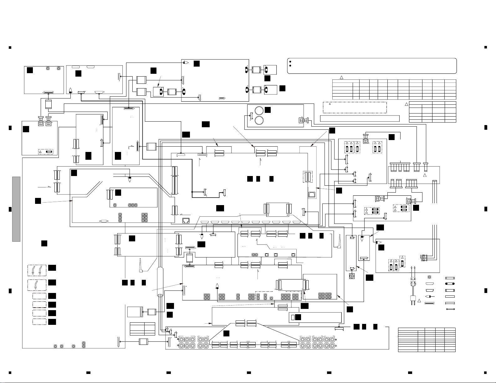
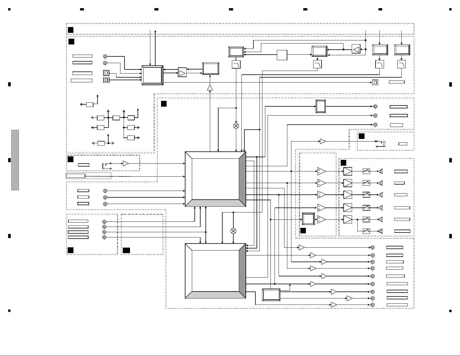
4. BLOCK DIAGRAM
4.1 OVERALL WIRING DIAGRAM
5
6 7 8
SC-99
15
F
E
D
C
B
5
6 7 8
A
Page 16
16
COAX2(SAT/CBL)
OPT IN1(TV)
OPT IN2(DVR/BDR)
COAX1(DVD)
IC2009
8ch DAC
ES9016S
TX1
JA2002
JA2004
JA2006
MIC
SAT/CBL
CD
PREOUT FL/FR
PREOUT SW1
PREOUT SL/SR
PREOUT SBL/SBR
DVR OUT
SP FL/FR
SP C
SP SL/SR
SP SBL/SBR
HP
SW DownMix
JA3471
IC2701, IC2702
JA2505
SW PRE Amp
IC2751
<<POWER AMP>>
JA2504
JA3476
JA4101
JA4101
JA4301
JA4501
JA3101
JA3101
JA3201
JA3201
PREOUT C
JA3103
DVR
JA2501
ZONE3 OUT
JA3206
HEADPHONE Amp
IC6821,
IC6841
IC6801
IC6861,
IC6881
IC6901,
IC6921
<<PREOUT>>
<<AUDIO ZONE OUT>>
MIC Amp
IC3471
IC2032
(ZONE2)
LPF
I2S
A/D BUFFER
IC2033, IC2035
OPT OUT1
IC2801
JA2009
JA2505
PREOUT TML/TMR
JA3201
IC3221
PRE SELECTOR
SP TML/TMR
JA4901
TUNER Module
IC2003
DIR&DIT
AK4118AEQ
IC3271
IC7491
SELECTOR
IC2027
ADC
PCM1804DB
I2S(DATA)
I2S(BCK,LRCK)
SW PRE Amp
IC2751
JA3102
PREOUT SW2
PREOUT EX1L/EX1R
JA3202
IC3272
(FL,FR)
IC7451,
IC7471
SP EX1L/EX1R
JA5101
ZONE2
ZONE3
ZONE3
ZONE2 OUT
JA6701
IC2026
ZONE2 DAC
AK4388ET
ARC
IC2006
BUFFER
IC2007
BUFFER
I2S I2S
IC2010
8ch DAC
ES9016S
I-V
&
LPF
X2001
80 MHz
OSC
(Zone2 L,R)
(S&FH DATA)
(BCK, LRCK, F&C DATA)
(BCK, LRCK)
Except Japanese Model
IC2034
IC2031
IC2029
IC2030IC2037
IC2028
IC2002
IC2010
IC2009
V+6V_ADAD
IC2026,
IC2027
IC2009
,
IC2010,
X2001
IC2027
IC2009
,
IC2010
V+5V_D
IC2003,IC2004,
IC2005,IC2006,
IC2007
IC2001,
IC2003
1.2V
1.2V
3.3V
3.3V
3.3V
3.3V
5V
<<POWER AMP INPUT
BUFFER>>
LPF
IC2038
HD ZONE DAC
AK4388ET
I2S
IC2039
(HD ZONE2)
(HD Zone L,R)
IC2038,
IC3101
IC3151
IC3201
IC3251
IC2501
Selector / Volume / PRE Amp
BD3473KS2
IC3273
Selector / Volume / PRE Amp
BD3473KS2
MULTI IN L/R
MULTI IN C/SW
MULTI IN SBL/SBR
JA7761
JA7762
MULTI IN SL/SR
JA7761
JA7762
SC-99,SC-LX89 only SC-99, SC-LX89 only
IC2011, IC2012, IC2021(SR,EX1R)
IC2013, IC2014, IC2022(FR,SW1)
IC2015, IC2016, IC2023(C,FL)
IC2019, IC2020, IC2025(EX1L,SL)
IC2051, IC2052, IC2053 (SBL,SBR)
IC2041, IC2042 (SW2)
IC2017, IC2018, IC2024 (EX2L,EX2R)
(SBL,SBR,SW2,EX2L,EX2R)
(SB, EX2, SW2 DATA)
IC2036
X2001
3.3V
V+5R6_DDD
(C,SW1,SL,SR,EX1L,EX1R)
F
C
S
EX1
SW1
SW2 DownMix
IC2703, IC2704
(EX2L,EX2R)
)
(SBL,SBR,SW2)
SW2
SB
EX2
IC6761
JA3202
PREOUT EX2L/EX2R
IC2802
BD3812F
Z2VOL
DVR
(SW) (C/SW)
Refer to the “4.4 BLOCK DIAGRAM FOR DIGITAL MAIN AUDIO BLOCK”
TMEX1
TMEX1
I-V
&
LPF
DAC HIGH ASSY
B
MIC HP ASSY
K
MIC HP ASSY
K
AUDIO ASSY
A
D AMP ASSY
S
IR BUFFER_M
ASSY
P
DIGITAL MAIN ASSY
G
MULTI CH IN ASSY
E
MCH BRIDGE ASSY
AH
F
E
D
C
B
A
4.2 BLOCK DIAGRAM FOR AUDIO BLOCK
2 3 4
1
SC-99
1
2 3 4
Page 17
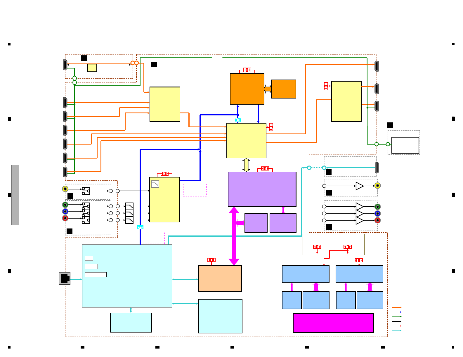
4.3 BLOCK DIAGRAM FOR DIGITAL MAIN VIDEO BLOCK
20 MHz
TMDS
DIGITAL VIDE O
CEC
ANALOG VIDEO
CLOCK
DIGITAL AU DIO
ETHERNET
IC9602
HDMI SW
Silicon Image
"SiI9589-3"
Deneb
IC909
Video Decoder
Analog
Devices
"ADV7181C"
EVENT ucom
RENESAS
IC102
SDRAM
64Mb
IC603
Gate Array
SEIKO EPSON
"PE7008A"
Media Processor
"AXX7293"
IC9202
Serial FLASH
128Mb
IC9206
iPod
Authentication
APPLE
(RENESAS)
"H337S3959"
2
2
2
2
36.864MHz
28.63636MHz
HDMI IN6
HDMI IN3
HDMI BDIN
(IN4)
HDMI IN1
HDMI IN2
HDMI IN5
COMPOSITE
COMPONENT
Pb
Pr
COMPONENT-Y
COMPOSITE
COMPONENT-Pb
COMPONENT-Pr
USB(FRONT)
CEC
HDMI OUT1
22.5792MHz
POWER SUPPLY BLOCK DIAGRAM
(DCDC,LDO)
Y
24.576MHz
HDMI IN7
/MHL
HDMI ZONE
/OUT3
24.576 MHz
IC1602
4k2k Upscaler
"MN864787"
IC101
uCOM
"R5S726B0D216FP"
IC9002
DSP
CS49844A
IC9001
SDRAM-166
64Mb(8Mx16)
IC9004
SeriFlash
32Mb
IC103
SerialFLASH
64Mb
12 MHz
27MHz
YCbCr422
16bit
IC9703
DSP
D808K013DPTP456
IC9702
SDRAM-166
64Mb(8Mx16)
IC9704
SeriFlash
16Mb
YCbCr422
16bit
For PQLS
DDC
Buffer
IC1204
IP.SCALER
Marvell
"88DE2750"
IC1212
DDR2
512Mb
IC1609
HDMI SW
"MN864788"
27MHz
HDMI OUT2
24 MHz
LAN PHY
Wi-Fi
BT
COMPOSITE ASSY
J
COMPONENT ASSY
I
FRONT HDMI USB ASSY
C
FRONT HDMI USB ASSY
C
DISPLAY ASSY
L
COMPOSITE ASSY
J
COMPONENT ASSY
I
DIGITAL MAIN ASSY
G
5
6 7 8
SC-99
5
6 7 8
17
F
E
D
C
B
A
Page 18
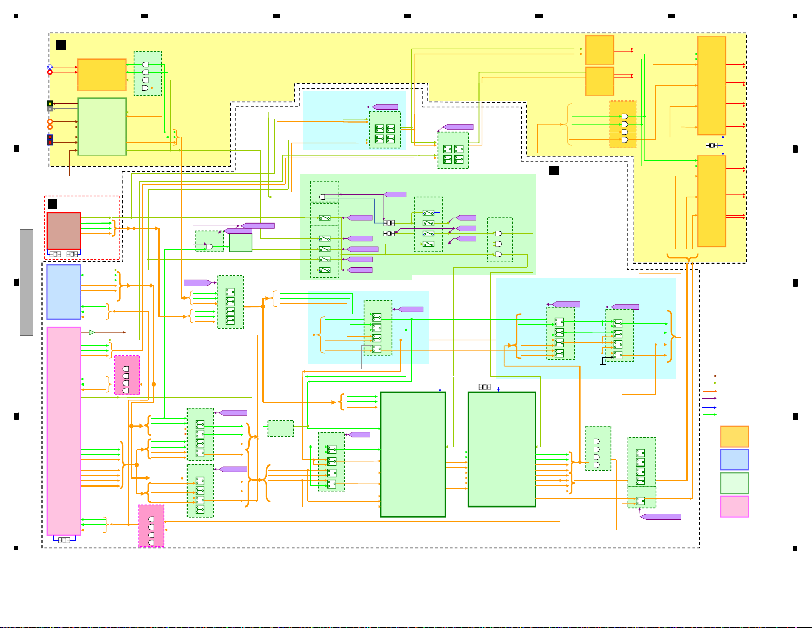
18
SPDIF
AMCLK
I2S
SYSCLK
FLG
I2S BCK,LRCK
HD ZONE DAC
SELECTOR
IC9006
SEL(VHC157)
SEL (7SZ126)
IC1512
IC2007
OR(VHC32)
IC2006
AND (VHC08)
IC2027IC2027
ADCADC
PCM1804DBPCM1804DB
IC2003IC2003
DIRDIR
AK4118AEQ8AK4118AEQ8
XTIXTI
MCKO1MCKO1
BICKBICK
LRCKLRCK
SDTOSDTO
DAUXDAUX
MSPDIF
COAX 1
COAX 2
OPT 1
OPT 2
27MHz
IC2010IC2010
DACDAC
ES9016ES9016
FL/FRFL/FR
C/LFEC/LFE
SL/SRSL/SR
FHL/FHRFHL/FHR
IC1602IC1602
MN864787MN864787
CH0AMCLK
USBUSB
DACDAC
NSLR/NDSDFR
NBCK
NLRCK
NFDAT/NDSDFL
NC_LFE
IC9101
SEL(VHC157)
H:USBDAC
L:DIR
24.0MHz
IC9703IC9703
2nd DSP2nd DSP
DA808K013DPTP456DA808K013DPTP456
ACLKR1
AFSR1
D1FDT AXR1[0]
D1CDT AXR1[1]
D1SDT AXR1[2]
D1BWDT AXR1[3]
D1HWDT AXR1[4]
D1DMDT AXR1[5]
AHCLKX0
ACLKX0
AFSX0
AXR0[7]D2FDT
AXR0[8]D2CDT
AXR0[9]D2SDT
AXR0[10]D2BWDT
AXR0[12]D2HWDT
AXR0[13]AMUTE
D2FDT/DSDFL
NET
POW
DIR
POW
DVC
POW
RYAC
XXTL0
AND (LCX08)
IC1804
SEL (VHC126)
IC1509
USBDMCK
HDMCK
DIRMCK
24.576MHz
22.5792MHz
SEL (VHC126)
IC1806
22PQLS
DAZDB
24PQLS
AND(LCX08)
IC1804
D2MCLK
AND(VHC08)
IC1601
NMPNMP
AXX7293AXX7293
ZNET
D_HN_DSDFR
D2CDT/DSDFR
D2SDT
D2BWDT
D2HWDT
D2LRCK
IC2026IC2026
Z2DACZ2DAC
FL/FRFL/FR
ZMCLK
DABCK
DALRCK/DSDFL
DAFDT/DSDFR
H: DIR
HDMI/NW HDMI/NW
SELECTORSELECTOR
IC1501
SEL(VHC157)
DSPPASS
D2BCK
D2LRCK
D2FDT/DSDFL
DIRMCK
DUBCK
L: NET/HDMI
NETMCK
IC1511
×8 or x4 PLL
NETDSDMCK
AND (SH08)
IC1521
DSD28X56
P1_BCK
P1_LRCK/DSDSL
P1_HFDT/DSDFL
P1_CDTI/DSDLFE
P1_BDTI/DSDSR
P1_DSDFR
D2B_BCK
D2B_LRCK
D2B_FDT
NMCK
UBBCK
UBLRCK
UBDATO
UBMCK
IC9002IC9002
1st DSP1st DSP
CS49844ACS49844A
DUBCK
DULRCK
DUDT
DAI3_SCK
DAI3_LCK
DAI3_D0
HN_CDTI/DSDLFE
HN_SDTI/DSDC
HN_BDTI/DSDSR
HN_DSDFR
DIRMCKI
IC1616
AND(VHC08)
DACDT
80MHz
SC-99,SC-LX89
only
DIRBCK
DIRLRCK
DIRDATO
SEL (LCX157)
IC1814
PHDZBCK
PHDZLRCK
PHDZFDT
PHDZMCLK
CH0ABCLK
CH0ALRCLK
CH0ASD0
CH0ASD1
CH0ASD2
CH0ASD3
CH0ASPDIF
P1_SDTI/DSDC
CH1ABCLK
CH1ALRCLK
CH1ASD0
Q6
Q5
Q4
Q0
D4
D1
D0
HDZBCK
HDZLRCK
HDZFDT
NSLR/NDSDFR
D2BCK
IC2038IC2038
HDZDACHDZDAC
FL/FRFL/FR
IC1516
SEL(VHC157)
DULRCK
IC2009IC2009
DACDAC
ES9016ES9016
SBL/SBRSBL/SBR
LFE2LFE2
ZONE-I2S (LR)
D2SW2DT
AXR0[11]
D2CDT/DSDFR
D_HN_BCK
HDZDACSEL
SEL (LCX157)
IC1818
H: NW/USB_DAC
L: HDMI
L: NETWORK
H: USB_DAC
AND(VHC08)
IC1603
D_HN_FDT/DSDFL
IC1815
SEL(VHC157)
NBCK
NLRCK
NFDAT/NDSDFL
NC_LFE
P1_BCK
P1_LRCK/DSDSL
P1_HFDT/DSDFL
P1_CDTI/DSDLFE
P1_BDTI/DSDSR
P1_DSDFR
P1_SDTI/DSDC
IC1817
SEL(LCX157)
DIRBCK
DIRLRCK
DIRDATO
UBLRCK
UBDATO
UBBCK
DUDT
IC1503
SEL(LCX157)
DSPB_BCK
DSPB_LRCK
DSPB_BDT
IC1507
SEL(WH157)
DSDXPCM
IC1515
SEL(LCX157)
DALRCK/DSDFL
DAFDT/DSDFR
DABCK
H : DSD
L : PCM
DACDT
24.576MHz
DSD_LRCK
DAI1_SCK1
DAI1_D1
DAI1_LRCK1
DAI1_D0
DAI1_D2
DAI1_D3
DAI1_D4
DAI1_D5
HN_DSD_LRCK
HN_HFDT/DSDFL2
HN_SDTI/DSDFR
HN_CDTI/DSDSL
HN_SDTI/DSDC
HN_BDTI/DSDSR
HN_CDTI/DSDLFE
FR_PRE_ON
DAO1_MCLK
DAO1_SCK1
DAO1_LCK1
DAO1_D0 D1FDT
DAO1_D2 D1CDT
DAO1_D1 D1SDT
DAO1_D3 D1EX1DT
DAO1_D4 D1EX2DT
DAO1_D5 D1EX3DT
NETDSDMC
L:NETMCK
H:HDMI
IC9005
VHC4040
D_HN_BCK
D_HN_LRCK
D_HN_FDT/DSDFL
HN_CDTI/DSDLFE
HN_SDTI/DSDC
HN_BDTI/DSDSR
HN_DSDFR
P1MCLK
D_HN_LRCK
HN_DIR_BCK
FMCLK
D2EXDT
DSP THROUGH PCM/DSD
SWITCHING BLOCK
H : DSP THROUGH ROUTE
L : DSP ROUTE
MASTER CLOCK SELECTOR BLOCK
ZONE DAC SELECTOR
USB DAC ASSY
F
DAC HIGH ASSY
B
DIGITAL MAIN ASSY
G
HDMCK
HDMCK
USBDMCK
DSD_IN
F
E
D
C
B
A
4.4 BLOCK DIAGRAM FOR DIGITAL MAIN AUDIO BLOCK
1
2 3 4
SC-99
1
2 3 4
Page 19
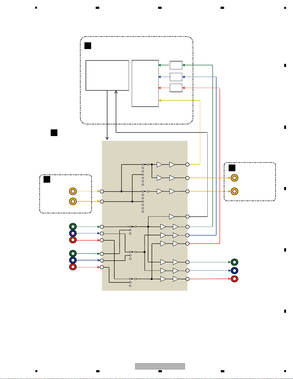
5
DVR
TV SAT
SH uCOMSH uCOM
"R5S726B0D216FP"
VDECVDEC
"ADV7181C"
LPF
LPF
LPF
50
47
14
16
17
19
20
22
31
38
33
32
30
29
28
37
39
26
IC8301
NJW1328FH2
CDET
I2C
MONITOR OUT
MONITOR OUT
DVR OUT
Y
Pb
Pr
IN1
IN2
(SC-99,LX89 only)
COMPONENT ASSY
I
COMPOSITE ASSY
J
COMPOSITE ASSY
J
DIGITAL MAIN ASSY
G
6 7 8
4.5 BLOCK DIAGRAM FOR VIDEO BLOCK
A
B
C
D
E
F
SC-99
5
6 7 8
19
Page 20
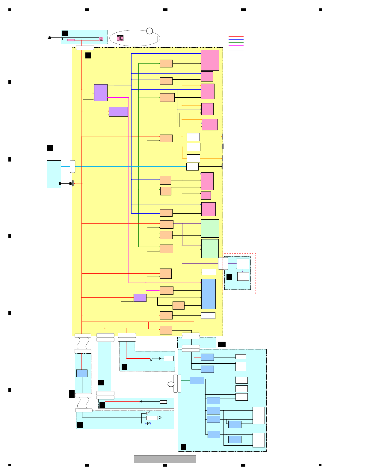
1
V+3R3_MA
V+1R25_MA
V+2R5_MA
DVCPOW
NETPOW
V+1R2_HD
V+1R1_PA
DVCPOW
JA1601
DVCPOW
JA1602
JA1603
V+5_MHL
JA9607
JA9620
V+1R8_SC
V+1_SC
V+1R8_VD
V+3R3_DSP
DIRPOW
DIRPOW
V+1_D1
DIRPOW
V+1R3_D2
V+3R3_OS
DIRPOW
V+1R2_NW
V+3R3_NW
NETPOW
V+2R5_NW
V+5_EV
V+5_DSP
DIRPOW
V+3R3_HHH(MA)
V+5R6_EV(DDD)
V+1R8_HHH
V+1R8_NW
NW Module
AXX7293
IC101
SH2
R5S726B0D216FP
IC103
Serial Flash
IC102
SDRAM
IC603
Gate Array
PE7008A
IC9002
CS49844A-CQZ
IC9001
SDRAM
IC9004
Serial Flash
IC909
VIDEO Decorder
ADV7181CBSTZ
IC9515
1.25V LDO
S-1172B1C-U5
IC9602
HDMI SW
SiI9589CTUC-3
IC1602
HDMI Tx
MN864787
IC9511
5V LDO
MM3529A50
IC9502
VARIABLE LDO
S-13A1A00-E6
IC9518
1V LDO
S-1172B10
IC9508
2.5V LDO
MM3529A25
V+5_HD
IC9505
1.8V LDO
MM3529A18
X1501, X1502
XTAL
IC9408
3.3V DCDC
MM3542BF
IC9403
1.1V DCDC Converter
MM3543BH
V+3R3_DSP
IC9603
Current SW
BD82065FVJ
IC451
3chDCDC
Converter
TPS65251RHA
IC9406
5V LDO
MM3411A50
232C
Mute Buffer
IC9703
DSP
D808K013DPTP456
IC9702
SDRAM
IC9704
Serial Flash
IC9407
2.5V LDO
MM3529A25
IC1615
5V LOAD SW
BD2242G-G
HDMI OUT1
HDMI OUT3/HDZONE
IC1605
5V LOAD SW
BD2242G-G
SMPS
Other Circuits
V+5R6_EV
Refer to
MAIN Transformer part
A
CN9501
CN9502
HDMI IN7/MHL
IC9523
1.2V Ripple
Blocker
MIC94325YMT
IC1609
HDMI TX SW 4in2
MN864788
IC1610
5V LOAD SW
BD2242G-G
HDMI OUT2
IC1204
VIDEO
PROCESSOR
88DE2750
IC1212
DDR2 for
Scaler
IC9402
1V LDO
S-1172B10
IC9404
1.8V LDO
MM3529A18
IC9513
3.3V LDO
NJM2846DL3-33
IC9514
1.3V Ripple
Blocker
MIC94325YMT
IC9512
3.3V LDO
NJM2872BF33
IR
IC9504
5V LDO
MM3529A50
EVENT CPU
V+5_EV
IC6001
CN7903
FFC
CN6001
V+5_EV
V+5R6_EV
CN7954
CN7004
CN7952
CN603
IC8601
RS232C
232POW
IC2003
DIR + DIT
Peripheral
AK4118AEQ
IC2026
Zone2 DAC
AK4388EF
IC2027
A/D Converter
PCM1804DB
IC2031
3.3V LDO
NJM2872BF33
C
N
2
0
0
4
V+3R3_DA
V+5_D
C
N
3
7
9
1
V+6_AD
C
IC2034
5V LDO
NJM2845DL1-05
V+5_D
V+3R3_D
IC2029
3.3V LDO
NJM2872BF33
IC2030
3.3V LDO
S-1172B33-E6
IC2009
SUB DAC
ES9016S
V+3R3_A
IC2010
MAIN DAC
ES9016S
V+3R3_DA2
IC2037
1.2V LDO
S-1172B12-E6
V+1R2_A2
IC2028
1.2V LDO
S-1172B12-E6
V+1R2_A
CN8301
CN901
IC7902
5V LDO
MM3411A50
IC2038
HDZone DAC
AK4388EF
IC2040
3.3V LDO
S-1172B33-E6
V+3R3_DA3
CN601
FFC
CN7902
CN9701
CN2001
CN3784
CN3783
IC2036
3.3V LDO
NJM2872BF33
V+3R3_DAOSC
X2001
XTAL
CN1984
CN5501
USBDPON
IC5503
USBDAC
CM6631
Q5622
FET SW
RTQ040P02
SC-99, SC-LX89 only
IC2002
3.3V LDO
NJM2881F33
FRONT HDMI
USB ASSY
DISPLAY ASSY
PRIMARY ASSY
C
L
T
DAC HIGH ASSY
INTERFACE_M ASSY
COMPONENT ASSY
CONNECT_M ASSY
B
H
I
Y
DISPLAY BRIDGE ASSY
AF
USB DAC
ASSY
F
D-DAC BRIDGE ASSY
AD
DIGITAL MAIN ASSY
G
2 3 4
4.6 BLOCK DIAGRAM FOR POWER BLOCK (1)
A
B
C
D
E
F
20
1
2 3 4
SC-99
Page 21
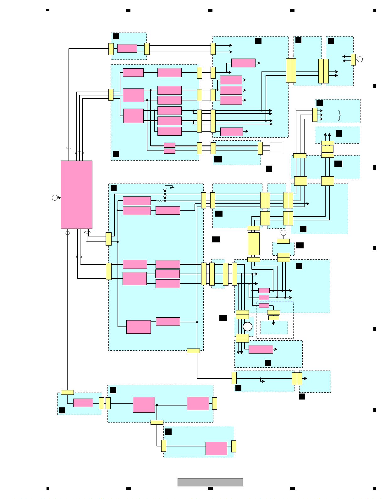
5
MAIN
Transformer
RECTIFIER
D7601
IC7601
NJM78M05FA
RECTIFIER
D7611-7613,C7611
IC7611
NJM78M12FA
5
CN7601
5
+
-
+
+
-
V+12A
V-12A
V+6AD
V+5V
AC1,AC2
-VF
CN7502
V+12TRG
2
for FL
V+12_A
V-12_A
TUNER MODULE
CN3902
FFC
V+5_T
V+7_A
V-7_A
V-12_A
V+12_A
V+5_DA
V+5_V
CN3001
CN3792
CN3791
CN2004
FFC
CN8301
CN901
V+5_V
A
RECTIFIER
D7521,7522
CN7501
+
CN7602
CN7721
CN7683
CN7681
CN7002
CN7603
CN7724
CN2503
CN7684
CN7722
CN7682
CN7007
CN7005 CN7008
CN7662 CN7661
CN7664
CN7663
FFC
CN3472
V-7_A
V+7_A
V+12TRG
AC1,AC2
-VF
V+5_V
CN7201
8
+
+
+
-
-
CN7241CN7271CN7291
FAN
-B+15V
V+8_MD
V-8_MD
V+FAN
V-FAN
V+12DF
V-12DF
3
CN7400
+
-
+B
-B
CN4001CN4002CN4003
V+64V
V-64V
VSS+12V
V+12V
V-12V
V+12RY
V-12RY
V+12**
V-12**
CN3801,3802
CN6802,6803
CN6801
CN3810-3890
CN4*00
CN6952
CN3051
CN6951
B
B
V+7_A
V-7_A
CN7401
IC4*03
NJM2830U1-12
Driver IC VCC
CN5932
CN5931
CN5775
IC2183
NJM2845DL1-05
RECTIFIER
D3651
+
CN3653
CN3652
C
V+5_USB
USB +5V
Supply
V+UN_USB
HDMI V+5MHL
Supply
JP8001
IC9603
BD82065FVJ
(Load SW)
JA9607
CN9502
CN8001
IC8004
BD9329EFJ
(DC-DC
Converter)
JA8001
IC8002
BD82065FVJ
(Load SW)
V+5_MHL
IC7241
NJM78M15FA
RECTIFIER
D7400,7401
V+6V
V-6V
IC4008
NJM78M06DL1A
IC4009
NJM79M06DL1A
IC4003
NJM78M05DL1A
V+5V_S
RECTIFIER
D7241-7244
IC7271
NJM78M08FA
IC7272
NJM79M08FA
RECTIFIER
D7271-7274
RECTIFIER
D7251-7254
IC7251
NJM78M12FA
IC7252
NJM79M12FA
IC7273
NJM78M15FA
CN7251
CN4004
Q7211
Q7212
V+15VDD
IC4002
NJM2830U1-12
V+12VD
JP7725
RECTIFIER
D7621-7623,C7621
JP5775
JP3001
IC7521
NJM78M06FA
IC7501
NJM78M12FA
IC7502
NJM79M12FA
RECTIFIER
D7501-7504
Q3002
Q3001
Q3901
Except Japanese Model
JP8401
JP6001
C
D
A
B
H
I
K
L
P
R
S
V
W
X
Z
AA
AB
AE
AG
AI
AK
AUDIO ASSY
DAC HIGH ASSY
FRONT HDMI USB ASSY
USB RECT_M ASSY
INTERFACE_M ASSY
COMPONENT ASSY
MIC HP ASSY
DISPLAY ASSY
IR BUFFER_M
ASSY
IR
INTERFACE_M
ASSY
D AMP ASSY
REG ASSY
IR REG_M ASSY
B DIODE ASSY
FB CONNECT
ASSY
PRE BRIDGE_M
ASSY
A-DAC
BRIDGE
ASSY
FRONT BRIDGE
ASSY
F-IN BRIDGE
ASSY
A REG
BRIDGE
ASSY
FAN CONNECT ASSY
DIGITAL MAIN ASSY
G
DIGITAL MAIN ASSY
G
6 7 8
4.7 BLOCK DIAGRAM FOR POWER BLOCK (2)
A
B
C
D
E
5
SC-99
6 7 8
F
21
Page 22
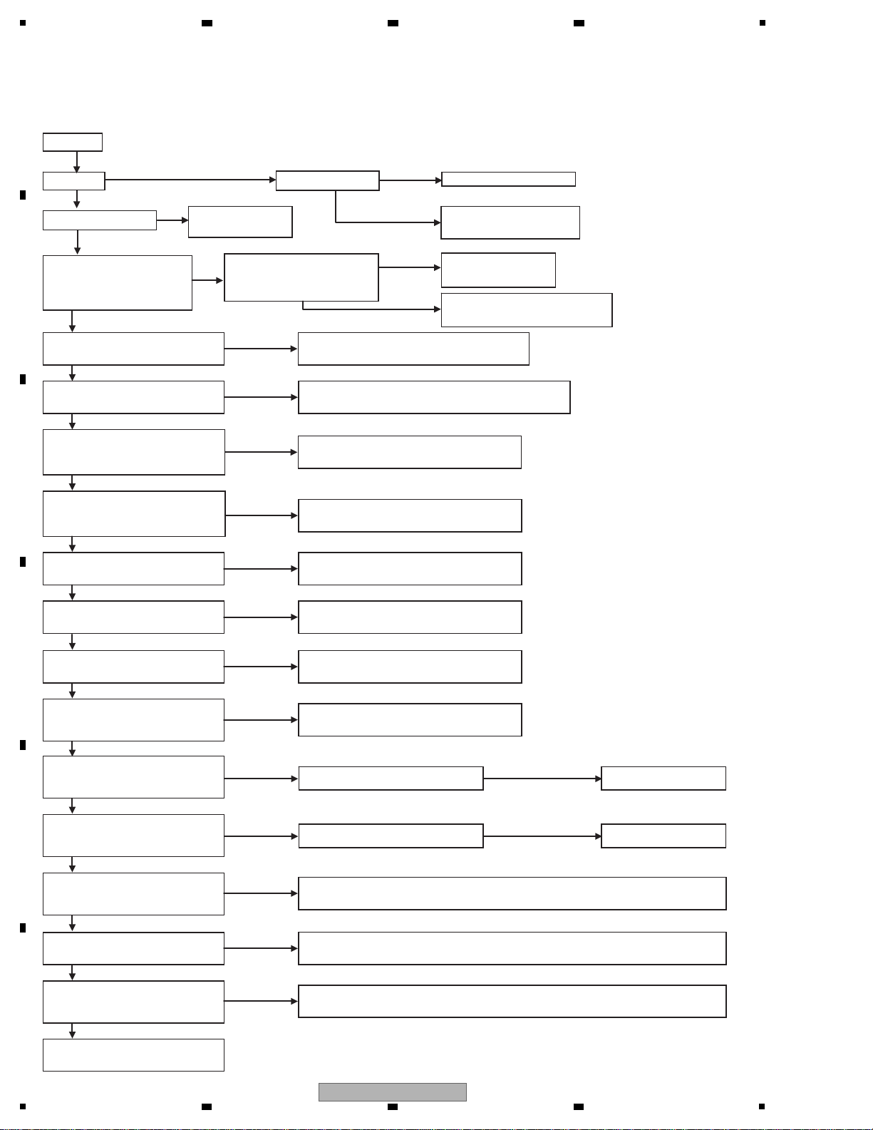
1
This is just for general reference and does not including every single case.
No Power
Error Indications ?
Stand by
No
Yes
Yes
No
Refer to the
“5.2 [4] Error Indocations”
Jump to “No FL DISPLAY”
Fuse FU4 OPEN ?
No
Yes
Diagnose or replace
PRIMARY ASSY
Check PRIMARY ASSY
JP51-1,2,3pin or DIGITAL
MAIN ASSY
CN9501-1,2,3pin +5.6V
No
Check DIGITAL MAIN ASSY
CN601-1,2pin +5.6V
Check +5.6V line on DIGITAL MAIN ASSY
or replace DIGITAL MAIN ASSY
Check DISPLAY ASSY
C6017 +3.3V
Replace DISPLAY ASSY
or replace L6001
Yes
Yes
Yes
Yes
Yes
Check DISPLAY ASSY
L6001 +5.0V
Replace DISPLAY ASSY
or replace IC6002
Check DISPLAY ASSY
IC6001-10pin +4.9V (XRESET)
Check the signal path of XRESET
or replace DISPLAY ASSY
Check DISPLAY ASSY
IC6001-32pin (POWKEY)
HL when press power key
Check the signal path of POWKEY
Check DISPLAY ASSY
CN6001-16pin (DVCPOW)
LH when press power key
Check the signal path of DVCPOW
No
Check DISPLAY ASSY
CN6001-12pin (ACRY)
LH when press power key
No Problem
Replace DISPLAY ASSY
Check the signal path of ACRY
Check PRIMARY ASSY
JP51-7pin (ACRY)
LH when press power key
Does RY71 turn on
when press power key ?
Remove AC code and remove
CN9501. Insart AC code and
check JP51-1,2,3pin, +5.6V
Diagnose or replace
PRIMARY ASSY
No
Diagnose the power supply path of
V+5R6_EV after PRIMARY ASSY
Yes
Check DISPLAY BRIDGE ASSY
CN7902-38,39pin +5.6V
Replace FFC
(DIGITAL MAIN ASSY to DISPLAY BRIDGE ASSY)
Check DISPLAY BRIDGE ASSY
CN7903-1,2pin +5.0V
CN7903-36pin +4.9V(XRESET)
Check DISPLAY ASSY
CN6001-38,39pin +5.0V
CN6001-4pin +4.9V(XRESET)
Replace DISPLAY BRIDGE ASSY,
D7901, IC7901, IC7902 or IC7903
Replace FFC
(DISPLAY BRIDGE ASSY to DISPLAY ASSY)
No
No
No
No
No
Yes
No
Yes
No
No
Yes
No
Yes
No No Problem
Replace DISPLAY ASSY
Yes
Yes
No
Yes
Yes
No
Yes
Check the signal path of ACRY DISPLAY ASSY DISPLAY BRIDGE ASSY
DIGITAL MAIN ASSYPRIMARY ASSY
Check the circuits around RY71 or replace PRIMARY ASSY
Check DIGITAL MAIN ASSY
CN601-16pin (DVCPOW)
LH when press power key
Check the signal path of DVCPOW DISPLAY ASSY DISPLAY BRIDGE ASSY
DIGITAL MAIN ASSY
Diagnose or replace
DIGITAL MAIN ASSY
2 3 4
5. DIAGNOSIS
5.1 DIAGNOSIS FLOWCHART
NO POWER
A
B
C
D
E
F
22
1
SC-99
2 3 4
Page 23
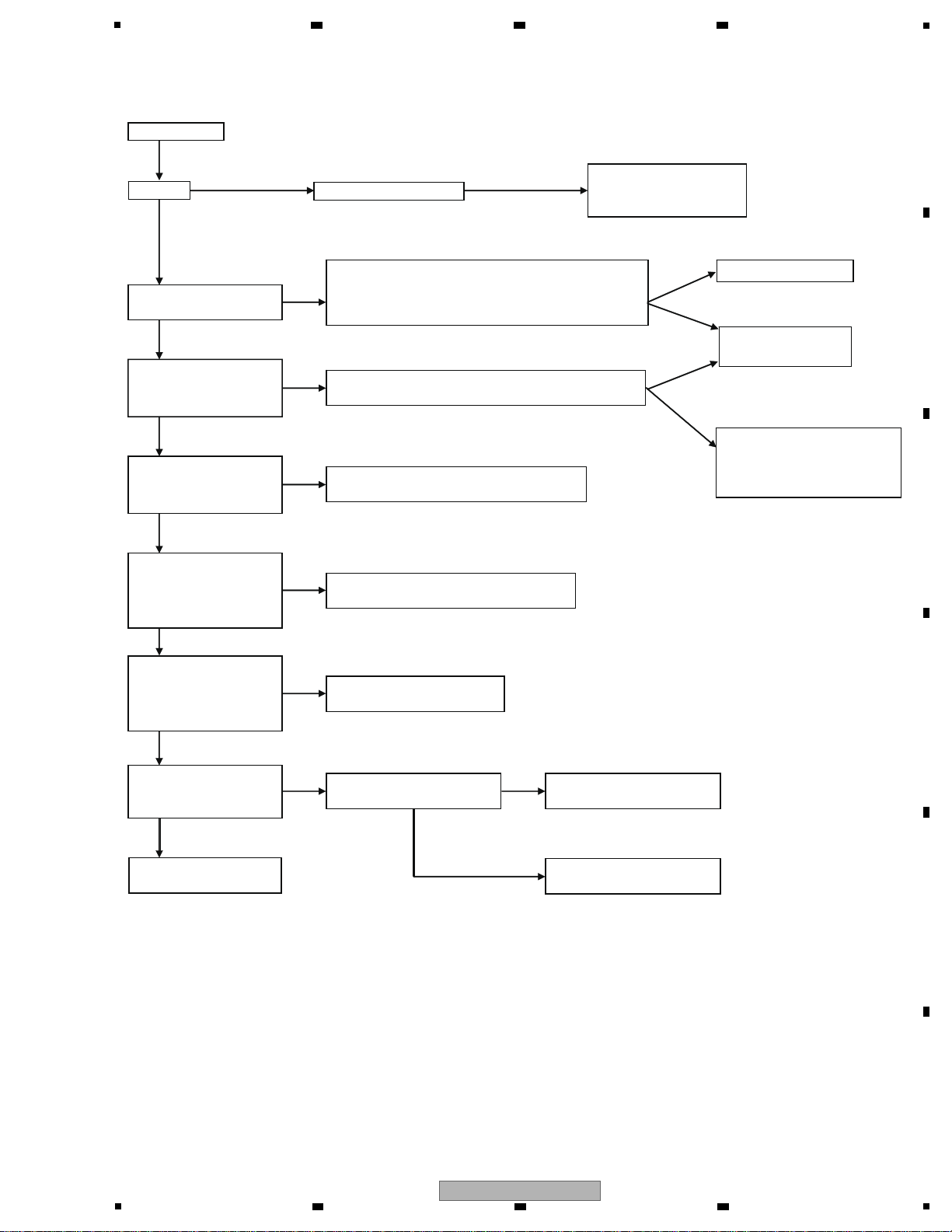
5
This is just for general reference and does not including every single case.
No FL DISPLAY
Dimmer ?
No
"FL OFF" LED light on ?
Yes No
JP6001 6,7pin 4.3Vac
Yes
No
V6001(FL Display)
damage
Yes
No
Yes
Replace V6001
(FL Display)
Check the power supply path of FL AC1
and AC2 or replace DISPLAY ASSY
Check DISPLAY ASSY
Check DISPLAY ASSY
JP6001 5pin -30V (VF)
4pin +5V
No
Yes
Check the path of V+5_V,-VF
(Signal path is same as FL AC1 and AC2)
All NG
All NG
Replace MAIN TRANS
Diagnose or replace
NG ASSY
Other results
Other results
Diagnose the circuits
(around D6010)
or replace DISPLAY ASSY
Diagnose around IC6003
NG
Replace IC6003
or DISPLAY ASSY
No Problem
Replace V6001(FL Display)
or DISPLAY ASSY
Check DISPLAY ASSY
Check DISPLAY ASSY
Yes
No
No
Replace IC6003
or DISPLAY ASSY
Diagnose REG ASSY
(around IC7601:V+5_V, D7625,
D7267:-VF) or replace
REG ASSY
Check the path of FL AC1 and AC2
DISPLAY
F-IN BRIDGE INTERFACE_M
FB CONNECT
FRONT BRIDGE REG
MAIN TRANS
Check DISPLAY ASSY
V6001(FL Display)
1,62pin 4.3Vac
Check DISPLAY ASSY
IC6003(FL uCOM)
56pin +5.0V (V+5_V),
IC6003(FL uCOM)
51pin (OSC1)
52pin +5.0V (XFLRST)
Check the path of V+5_V or XFLRST
or replace DISPLAY ASSY
No
Yes
Oscillating 2MHz
6 7 8
NO FL DISPLAY
A
B
C
D
5
SC-99
6 7 8
E
F
23
Page 24
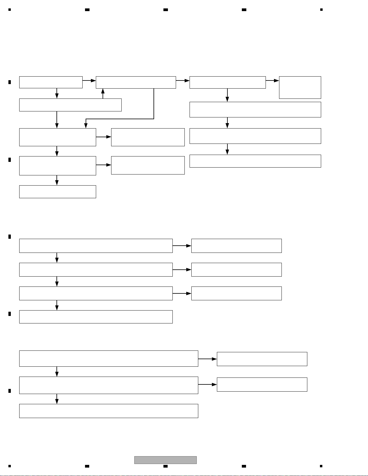
1
EXT STEREO mode : 2ch signals are distributed to all channels.
OPTIMUM Surr mode : Surround mode of headphones
No sound from speakers (Single channel - Check only the signal path of the relevant channel. Plural channels
- There may be troubles with power source, control signals: MUTE, DET and others. Bad connection of cables
and connectors should be also considered.)
No sound only from front
channels (L/R 2 channels)
The sound of the relevant
channel does not come from Preout.
Sound comes from speakers in Pure Direct by
applying a signal to analog input terminal.
The signal of the relevant channel
exists in PRE BRIDGE_S ASSY.
Check the path of
the relevant
channel in AUDIO
ASSY.
Check the signal path of the relevant channel in
IR BUFFER_M ASSY, or check the path of the power supply
to the relevant channel.
In EXT STEREO, the signal of the
relevant channel does not exist in
A-DAC BRIDGE ASSY.
Check the path of the relevant
channel in AUDIO ASSY.
Check the signal path of the relevant channel in
IR INTERFACE_M ASSY, or check the path of the power
supply to the relevant channel.
The signal (DATA, BCK, LRCK) of
the relevant channel does not exist
in D-DAC BRIDGE ASSY.
Check the path of the relevant
channel in DAC HIGH ASSY.
Check the path of the relevant channel in
D AMP ASSY.
Check the path of the relevant
signal in DIGITAL MAIN ASSY.
No sound only from Preout (Single channel - Check only the signal path of the relevant channel. Plural channels
- There may be troubles with power source, control signals: MUTE, DET and others. Bad connection of cables
and connectors should be also considered.)
No sound only in DVROUT or PHONO - Check the relevant path in AUDIO ASSY .
No sound from speakers additionally
Check the path of the relevant channel
in AUDIO ASSY.
In EXT STEREO, the signal of the relevant channel does not exist in
A-DAC BRIDGE ASSY.
Check the path of the relevant channel
in AUDIO ASSY.
The signal (DATA, BCK, LRCK) of the relevant channel does not exist
in D-DAC BRIDGE ASSY.
Check the path of the relevant channel
in DAC HIGH ASSY.
Check the path of the relevant signal in DIGITAL MAIN ASSY.
No No No
Yes
Yes
Yes
Yes
Yes
Yes
OK
OK
No
No
No
Yes
Yes
Yes
No
No
No
No sound only in COAX and OPT input (Single channel - Check only the signal path of the relevant channel.
Plural channels - There may be troubles with power source, control signals: MUTE, DET and others.
Bad connection of cables and connectors should be also considered.)
Check the path of the relevant channel
in DAC HIGH ASSY.
Check the path of the relevant signal in DIGITAL MAIN ASSY.
Yes
No
Check the path of the relevant channel
in DAC HIGH ASSY.
Yes
No
Apply a signal to analog input terminal but not output from preout
and SPEAKER in AutoSurr.
Return to COAX and OPT input but DIRDATO, DIRBCK,
DIRLRCH and DIRMCKO of D-DAC BRIDGE ASSY are not existed.
2 3 4
NO SOUND (Except for troubles caused by setting and others)
A
B
C
D
E
F
24
1
2 3 4
SC-99
Page 25
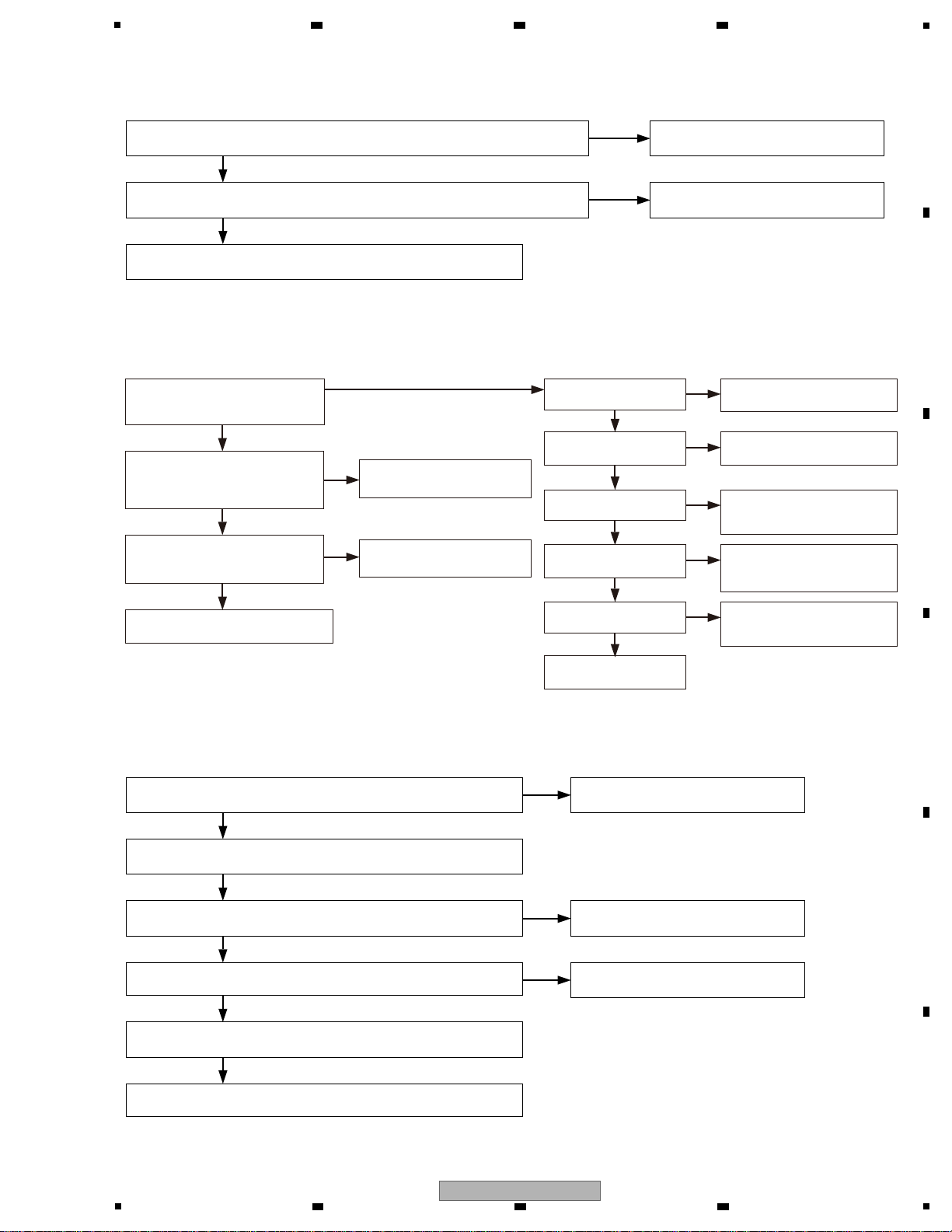
5
No sound only in AutoSurr in analog input (Single channel - Check only the signal path of the relevant channel.
Plural channels - There may be troubles with power source, control signals: MUTE, DET and others.
Bad connection of cables and connectors should be also considered.)
Apply a signal to COAX and OPT input terminal but not output
from preout and SPEAKER in AutoSurr.
Check the path of the relevant channel
in DAC HIGH ASSY.
Return to AutoSurr of analog input but DIRDATO, DIRBCK, DIRLRCK,
DIRMCKI and DIRMCKO of D-DAC BRIDGE ASSY are not existed.
Check the path of the relevant channel
in DAC HIGH ASSY.
Check the path of the relevant signal in DIGITAL MAIN ASSY.
No sound from HEADPHONES (Single channel - Check only the signal path of the relevant channel. Plural channels -
There may be troubles with power source, control signals: MUTE, DET and others. Bad connection of cables and
connectors should be also considered.)
If it is impossible to change to HEADPHONE, check the path of XHPDET signal.
No sound only from ZONE (Single channel - Check only the signal path of the relevant channel. Plural channels -
There may be troubles with power source, control signals: MUTE, DET and others.
Bad connection of cables and connectors should be also considered.)
No sound only in ZONE SW - Check the relevant path in AUDIO ASSY.
Sound comes from ZONE2 or ZONE3 OUT by applying the signal to
analog input terminal.
Check the path of the relevant channel
in AUDIO ASSY.
If music content is replayed with Front USB terminal, sound does
not from ZONE2.
In AutoSurr, the signal of the relevant channel exist in
A-DAC BRIDGE ASSY.
Check the path of the relevant channel
in AUDIO ASSY.
The signal(ZFDA, ZBCK, ZLRCK, ZMCK) of the relevant
channel does not exist in D-DAC BRIDGE ASSY.
Check the path of the relevant channel
(ZONE2 DAC) in DAC HIGH ASSY.
Check the path of the relevant signal in DIGITAL MAIN ASSY.
Check the path of the relevant signal in FRONT HDMI USB ASSY.
Yes
Yes
No
No
Yes
Yes
Yes
Yes
Yes
No
No
No
Sound comes from HEADPHONE
in Pure Direct by applying a signal
to analog input terminal.
Sound comes from
Preout in PureDirect.
Check the path of the relevant
channel in AUDIO ASSY.
In AutoSurr with removing
HEADPHONE, the signal of the
relevant channel does not exists in
A-DAC BRIDGE ASSY
Check the path of the relevant
channel in AUDIO ASSY.
HP signal exists in
FRONT BRIDGE ASSY.
Check the path of the relevant
channel in AUDIO ASSY.
The signal(DATA, BCK, LRCK) of
the relevant channel does not
exist in D-DAC BRIDGE ASSY.
Check the path of the relevant
channel in DAC HIGH ASSY.
HP signal exists in
FB CONNECT ASSY.
Check the path of the relevant
channel in FRONT BRIDGE
ASSY.
Check the path of the relevant
signal in DIGITAL MAIN ASSY.
Check the HP signal
path in MIC HP ASSY.
No
No
No
No
Yes
Yes
Yes
Yes
Yes
Yes
HP signal exists in
INTERFACE_M ASSY.
Check the path of the relevant
channel in FB CONNECT
ASSY.
HP signal exists in
F-IN BRIDGE ASSY.
Check the path of the relevant
channel in INTERFACE_M
ASSY.
No
No
Yes
Yes
No
No
6 7 8
A
B
C
D
SC-99
5
6 7 8
E
F
25
Page 26
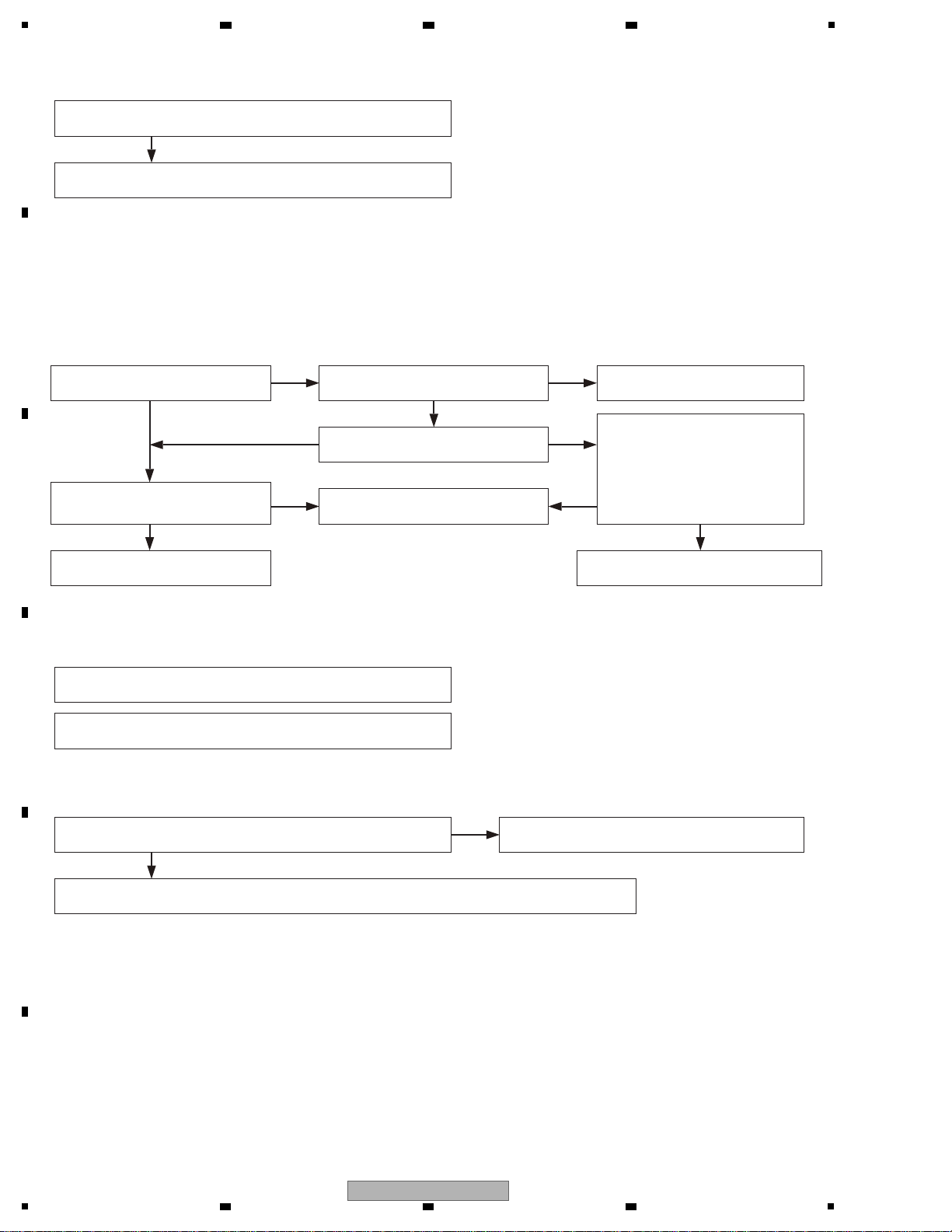
1
No sound only from FRONT USB terminal or only from MHL terminal (There may be troubles with the power
source of circuit and control signals. Bad connection of cables and connectors should be also considered.)
Check the path of the relevant signal in FRONT HDMI USB ASSY.
Check the path of the relevant signal in DIGITAL MAIN ASSY.
No sound only in HDMI, MEDIA SERVER and INTERNET RADIO (There may be troubles with the power source of
circuit and control signals. Bad connection of cables and connectors should be also considered.)
Check the path of the relevant signal in DIGITAL MAIN ASSY.
No sound only in BT (Single channel - Check only the signal path of the relevant channel. Plural channels -
There may be troubles with power source, control signals: MUTE, DET and others. Bad connection of cables
and connectors should be also considered.)
No sound only in tuner (There may be troubles with the power source of circuit and control signals.
Bad connection of cables and connectors should be also considered.)
No sound only in MULTI CH IN (There may be troubles with the power source of circuit and control signals.
Bad connection of cables and connectors should be also considered.) (SC-97, SC-LX79 only)
Check the path of the relevant channel in AUDIO ASSY, and check TUNER MODULE.
Yes
The signal of the relevant channel(2, 4, 6, 8, 10, 12, 14 and 16pin)
exists in CN2510
Yes
No
No sound only in USB-DAC (There may be troubles with the power source of circuit and control signals.
Bad connection of cables and connectors should be also considered.) (SC-99, SC-LX89 only)
Check the path of the relevant signal in USB DAC ASSY.
Check the path of the relevant signal in DIGITAL MAIN ASSY.
Check the circuit of the connection destination.
Check the broken point (start with checking the relevant channel (FL, FR, C, SW, SL, SR of
IC2501 and SBL, SBR of IC3273), and check the peripheral circuit.
Yes
Yes
Yes
No
Yes
No
No
OK
No
Is the Antenna (ADH7049) connected to
the Network Module(AXX7293)?
Is the Home Menu OSD displayed?
Remove the Network Module
(AXX7293) and check the following
voltages of CN9203
1pin or 3pin :1.2V /
2pin or 4pin : 2.5V /
7pin or 9pin : 1.8V /
8pin or 10pin : 3.3V
Check the Power IC for problem voltage
or replace the DIGITAL MAIN ASSY
Connect the Antenna (ADH7049)
to Network Module (AXX7293)
Replace the Network Module(AXX7293)
Check the degital audio signal output
(CN9203 - 26, 28, 30, 32, 34pin) of
DIGITAL MAIN ASSY
Can it connect (paring) with any BT
Devices?
No Good
Replace the DIGITAL MAIN ASSY
A
2 3 4
B
C
D
E
F
26
SC-99
1
2 3 4
Page 27
5
No sound only in POWERD HD ZONE
Speaker setting is correct ? Set the Speaker setting correctly.
Is there signal in the CN9702-22, 24, 25, 26pin of
DIGITAL MAIN ASSY ?
Check the peripheral circuit of IC1818.
Check the path from IC1602.
Is there signal in the IC2038-1, 2, 3, 4pin of
DAC HIGH ASSY ?
Check the peripheral path.
Check the VOL IC(IC2501, IC3273) peripheral circuit of
AUDIO ASSY.
Yes
Yes
Yes
Yes
No
No
No
Check the peripheral circuit of IC2038.
Is there signal in the CN2003-1, 3pin of DAC HIGH ASSY ? Check the peripheral circuit of IC2039.
Yes
No
No
Is there signal in the IC2038-10, 11pin of DAC HIGH ASSY ?
No sound by MEDIA SERVER, INTERNET RADIO, FRONT USB, BT and Wi-Fi
Yes
No
Yes
No
Yes
No
Check the Power IC for problem voltage or
replace the DIGITAL MAIN ASSY
Check the connection between DIGITAL MAIN ASSY and
Network Module (AXX7293)
Reconnect the Network Module(AXX7293) to
DIGITAL MAIN ASSY.
Check the digital audio signal lines or
replace the DIGITAL MAIN ASSY
Replace the Network Module(AXX7293)
Check the degital audio signal output (CN9203 - 26, 28, 30, 32, 34pin)
of DIGITAL MAIN ASSY
Remove the Network Module (AXX7293) from DIGITAL MAIN ASSY
and check the following voltages of CN9203 - 1pin or 3pin :1.2V / 2pin
or 4pin : 2.5V / 7pin or 9pin : 1.8V / 8pin or 10pin : 3.3V
6 7 8
A
B
C
D
E
5
6 7 8
SC-99
F
27
Page 28
1
No sound only in PHONO
Check the path and circuit between IC2501 and JA2503.
No sound in plural input modes of speaker and Preout
No sound in plural channels
Check the broken point (start with checking the
relevant channel of CN2502)
Check of power source: Is there ±12V in JP3001 ? Check the circuit of the connection destination.
7V and -7V are output from Q3001 and 3002. Check the circuit.
MUTE signal of the relevant channel of CN2861 is "L".
Check the circuit of the connection destination.
When CN2861 volume is changed, the signal is
transmitted to 11, 12, 13pin.
Check the circuit of the connection destination.
Check the broken point (start with checking the relevant
channel of CN2502), and check the peripheral circuit.
No sound only in analog input
Check the path from each input terminal to IC2501.
No sound only from HEADPHONES
Check the peripheral of IC2801.
No sound only from ZONE 2 and ZONE 3 (Both of them, Either of them)
MUTE signal of the relevant channel of CN2861 is "L." Check the circuit of the connection destination.
When CN2861 ZONE volume is changed, the signal is
transmitted to 11, 13pin.
Check the circuit of the connection destination.
Check the broken point (start with checking the relevant channel (34, 35, 77, 78pin of
IC2501), and check the peripheral circuit.
No sound only from ZONE 2 of FRONT USB
Check the path from 1, 3pin of CN2502 to IC2501.
No sound only in BT
Check the path from 18, 20pin of CN3001 to IC2501.
No sound only in Tuner
The signal is transmitted to 7, 9pin when CN3902 is in
reception state.
Check or repalce TUNER MODULE.
5V is output from Q3901. Check the circuit.
When the frequency of the tuner of CN3902 is changed, the
signal is transmitted to 1, 2, 3, 4pin.
Check the signal path between
CN3902 and CN2861.
Check the signal path form CN3902 to IC2501.
No sound only from DVR/BDR OUT
Check the path and circuit between IC2501 and JA2501.
No
No
No
No
No
Yes
Yes
Yes
Yes
No
No
No
Yes
Yes
Yes
Yes
No
No
Yes
Yes
2 3 4
AUDIO ASSY DIAGNOSIS
A
B
C
D
E
F
28
1
SC-99
2 3 4
Page 29
5
No sound from speakers and Preout in EXT STEREO
No sound in plural channels
Check the broken point (start with checking the
relevant channel of CN2003)
Check of power source: Is there ±12V in CN2004 ?
Check of power source: Is there ±6V in CN2004 ?
Check the circuit of the connection destination.
Check the circuit of the connection destination.
Check the circuit of the connection destination.
No sound only in analog input
Check the peripheral circuit of IC2027.
No sound only in COAX input or OPT input
Check the peripheral circuit of IC2003.
No sound only from ZONE 2 of FRONT USB
Check the peripheral circuit of IC2026.
No
No
No
No
No
Yes
Yes
Yes
Yes
Yes
Check the peripheral circuit of X2001.
The signal(DABCK, DALRCK, each DATA) of the relevant
channel exist in CN2001.
80MHz clock exist in 19pins of IC2009 and IC2010.
Check the broken point (start with checking the relevant
channel of CN2003), and check the peripheral circuit.
No sound only in BT
Check the 14, 16pin of JA2010, the power source and control signals.
DAC HIGH ASSY DIGNOSIS
6 7 8
A
B
C
D
E
5
SC-99
6 7 8
F
29
Page 30
1
1) No Sound
No
Yes
No
No
Yes
Yes
No
No
Yes
Yes
NOTE : Wiring number listed is the example of Front L-ch
2) Diagnosis Flow Chart from Error Symptom
Failure locating method from error symptom is available as diagnosis after product shutdown.
Diagnosis Flow Chart from error symptom due to Amplifier Section is shown here.
Cause of being BERR
When B-Power Supply Voltage exceeds
+
75 V
No
When B-Power Supply Voltage falls below +20 V
Yes
Cause of being OL
No
At Over Current Detected (Not worked with no-load)
At Driver IC not Oscillated
At ZOBEL Detection Circuit Activated
Yes
Cause of being DC
When DC 7V or above is output in Audio Output Line
Cause of being TEMPERR
When MOSFET Temperature exceeds approx. 120 degrees
When MOSFET temperature is suddenly increased
Shorted MOSFET (Q4101, Q4102)
Failure BERR Detection Circuit
(around Q4022, Q4024)
Check Connector Conductivity
Oscillation
Waveform on Driver IC
(IC4101) Output (13pin) seen
just in a moment
at restarting?
Parts Failure after AMPLPF
(L4100, C4101)
Failure in MOSFET (Q4101, Q4102)
Check Power Supply on
Temperature Detection Circuit
(around R4181 and Q4117)
Perform impedance check on
Audio Output Line vs. Power Supply
Failure around Driver ->
Replace Driver IC
Failure around ZOBEL Detection
Circuit (Q4104, etc)
Power
Distribution
Status
Any Switching
Residual Waveform existed
in Speaker Output* ?
(Sine wave = Approx.
450 KHz, 0.7V rms)
Audio Signal Input
Check how far the
signal is passing
MUTE cleared ?
Check MUTE Control
voltage (Q4109 Base)
V = -12V (Normally)
Go to 2) Diagnosis Flow Chart
from Error Symptom if immediate
shut down happens by the
Protection Circuit.
Check LPF COIL Conductivity
(L4100)
Check each Power Supply of
Driver IC (IC4101)
Check Relay (RY4100) is ON
Check MUTE Control Line
Signal exists just
before Driver IC (IC4101) ?
Check the four block ASSY of
D AMP ASSY
Failure Driver IC (IC4101)
Abnormality
Detection on
AMP Power
Voltage (BERR)
Over Current
Detection (OL)
DC Detection
TEMPERR
Check XBERR Line Conductivity
from D AMP ASSY
CN4000-6pin to DISPLAY ASSY
CN6001-31pin.
BERR Conductivity
Failure Detection
(CERR)
Approx. DC 2V
exists in
Speaker Output ?
Check Voltage of Driver IC
CSD Port (2pin)
DIGITAL AMP BLOCK FLOWCHART
(Waveform 1 and 2)*
* : Refer to D AMP ASSY (2/6)
There is a problem
in Conduction of Power
Supply Connector* ?
*: (CN4001, CN4002,
CN4003, CN4004)
*
Precautions for checking the speaker output
For the channel shown below, positive and negative of
SP terminal are inverted.
surround ch :
surround back ch :
The black terminal is HOT
and the red terminal is ground.
Parts Failure after AMPLPF (L4100, Q4101)
A
2 3 4
B
C
D
E
F
30
1
2 3 4
SC-99
Page 31

5
No Picture
Analog Video IN ?
Diagnose or replace
FRONT HDMI USB ASSY
Composite in
Composite out ?
Check
COMPONENT ASSY
CN8303 video signals
Diagnose COMPONENT ASSY
(around IC8301)
or replace COMPONENT ASSY
Diagnose COMPOSITE ASSY
(input circuits)
or replace COMPOSITE ASSY
Diagnose COMPOSITE ASSY
(output circuits)
or replace COMPOSITE ASSY
Component in
Component out ?
Front HDMI in
HDMI out ?
Diagnose or replace
DIGITAL MAIN ASSY
Composite
(Component) in
HDMI out ?
Diagnose or replace
DIGITAL MAIN ASSY
No GUI ?
HOME MENU GUI
USB GUI
NETWORK GUI
Diagnose DIGITAL MAIN ASSY
(around IC1602)
or Replace DIGITAL MAIN ASSY
No Problem
IN:NG,
OUT:NG
IN:OK,OUT:OK
IN:OK,
OUT:NG
HDMI IN3,IN4, IN6 and IN7
HDMI out ?
NG
OK
Check connection
(FRONT HDMI USB ASSY
DIGITAL MAIN ASSY)
Rear HDMI in
HDMI out ?
Diagnose or replace
DIGITAL MAIN ASSY
Check
DIGITAL MAIN ASSY
CN901 video signals
ONLY GUI ?
Replace Network Module (AXX7293)
NO
YES
This is just for general reference and does not including every single case.
In case of using 4K/60p-compatible TV and no picure.
The receiver’s HDMI input terminals support the 4K/60p signal. However, there are two types of terminals as follows.
Type 1: 4K/60p 4:4:4 24 bit signal (transmission speed up to 18 Gbps) can be transmitted: BD, DVD (HDMI IN 1), SAT (HDMI IN 2)
Type 2: 4K/60p 4:2:0 24 bit signal can be transmitted (4K/60p 4:4:4 24 bit signal is not supported, transmission speed up to 10.2 Gbps):
HDMI input terminals other than the above
NOTE: All input terminals are type 2 when HDZONE is turned on.
1. When a source device that does not support the 4K/60p 4:4:4 24 bit signal is connected to a type 1 terminal, the video image may become reddish,
sound may not be output, or 3D signals may not be output for some devices. For such devices, try the following.
*This is not a malfunction of the receiver.
Connect the device to a type 2 terminal instead of the type 1 terminal.
It is also possible to set all input terminals to type 2. Set the following “HDMI 4K/60p signal output setting” to “4:2:0”.
2. When the video image is not output, is interrupted, or there is noise, the cause may be the HDMI cable. (Some HDMI cables do not support
4K/60p 4:4:4 24 bit signal transmission.) In such cases, set the following “HDMI 4K/60p signal output setting” to “4:2:0”.
HDMI 4K/60p signal output setting
Operation is performed on the front panel of the unit. You cannot perform the setting if the multizone function is not set to MULTI ZONE OFF.
1 Switch the receiver into standby.
2 While holding down ENTER on the front panel, press STANDBY/ON.
The display shows RESET NO .
3 Use / to select ‘4K/60p’.
4 Use / to select the signal to set.
4:4:4 – Select this setting when connecting to a 4K/60p 4:4:4 24 bit compatible TV using HDMI. More high quality video images can be enjoyed.
4:2:0 – Select this setting when connecting to a 4K/60p 4:2:0 24 bit compatible TV using HDMI.
5 When you’re finished, press RETURN.
6 Press STANDBY/ON to switch on the receiver and your TV.
Make sure that the TV’s video input is set to this receiver.
6 7 8
NO PICTURE
A
B
C
D
5
6 7 8
SC-99
E
F
31
Page 32

1
This is just for general reference and does not including every single case.
12V Trig
RS-232C
IR
IR
RS-232C
Remote Control
No
Yes
No
No
Still NG
NG
Repair or replace
NG point
No Problem
12V Trig
Check INTERFACE_M ASSY
CN7002 4pin +12V
No
Yes
No
Check the power supply path of V+12_TRG
REG ASSYFRONT BRIDGE ASSY
FB CONNECT ASSYINTERFACE_M ASSY
ALL NG
Other results
Repair or
replace NG
point
Check the signal path of 232RX,232TX,232POW,232CDET
COMPONENT ASSY DIGITAL MAIN ASSY DISPLAY BRIDGE ASSY DISPLAY ASSY(IC6001)
and check the power supply path of V+5R6_EV
PRIMARY ASSY DIGITAL MAIN ASSY COMPONENT ASSY
Diagnose INTERFACE_M ASSY
(Circuits around Q7008,Q7010)
or replace INTERFACE_M ASSY
Diagnose COMPONENT ASSY
(around IC8601)
or replace COMPONENT ASSY
Diagnose INTERFACE_M ASSY(IR circuits)
or check the signal path of IR-IN
INTERFACE_M ASSY CONNECT_M ASSY DIGITAL MAIN ASSY
DISPLAY BRIDGE ASSY DISPLAY ASSY or replace INTERFACE_M ASSY
Check the signal path of
RMC
DISPLAY ASSY
Diagnose DISPLAY ASSY
(RMC signal path, around U6001,IC6001)
or replace DISPLAY ASSY
Diagnose REG ASSY
(Circuits around IC7611)
or replace REG ASSY
2 3 4
OTHER
A
B
C
D
E
F
32
1
SC-99
2 3 4
Page 33

5
[1] Protection Circuit Process List
Amplifier Circuit
Item Purpose Detection Method Status of Equipment Warning Indication Remarks
Overheat
detection
Detects MOS FET
temperature of amplifier output
stage
Detects when TEMPERR5 port
becomes "L" in case of the
detecting temperature exceeds
120°C or rapid change by short
cuicuit of speaker terminals.
(IC6001 24pin)
Blinks FL OFF LED
indicator.
Recoverable by power-on
after shutdown in 1 minute.
AMPTEMP voltage
[US Model Only]
5V-2.9V : FANLOW
2.9V or less : FANHIGH
[Except US Model]
5V-3.8V : FANSTOP
3.8V-2.9V : FANLOW
2.9V or less : FANHIGH
Detects when AMPTEMP port
becomes below 1.6V at NTC
Thermistor detect circuit.
(IC6001 64pin)
Fan rotates by power-on.
DC
detection
Detects DC of amplifier output
(After LPF)
Detects when SP output exceeds
DC ± 7V and XDCERR port
becomes "L". (IC6001 21pin)
MUTE on and Speaker
Relay off.
Flashes “AMP ERR”.
Shuts down when
abnormality continues for
more than 3 seconds.
MUTE on and Speaker
Relay off.
Flashes “AMP ERR”.
Shuts down when
abnormality continues for
more than 3 seconds.
Blinks MCACC PRO
LED
Blinks MCACC PRO
LED
Blinks FL OFF LED
indicator.
In case of detecting DC
abnormality during normal
operation. Recoverable by
power-on after 1 minute.
In case of detecting DC
abnormality during
power-on sequence after
the DC was once detected.
Recoverable by only DC
DETECT cancel.
Refer to “How to Enter
Release Mode” .
Recoverable by only DC
DETECT cancel.
Refer to “How to Enter
Release Mode” .
Fan
abnormality
detection
Detects a Fan not rotating by
loose connector or Fan lock
when controling the Fan rotation
Detects when XFANERR port
becomes "L". (IC6001 28pin)
Detects when XBERR port
becomes "M". (approx. 2.5V)
(IC6001 75pin)
Flashes "FAN STOP"
Shuts down when
abnormality continues for
more than 3 seconds.
Blinks Wireless LED
Blinks Wireless LED
Blinks Wireless LED
Recoverable by power-on
Recoverable by power-on
Recoverable by power-on
Zobel
detection
Protects overcurrent by Zobel
Resistance when high power
output of higher frequency
continued
Detects XOLERR port becomes
"L". (IC6001 13pin)
Shuts down
Shuts down
Shuts down
Overcurrent
detection
Protects overcurrent of MOS
FET in output stage when
overcurrent flows at the output
stage
Detects XOLERR port becomes
"L". (IC6001 13pin)
During Standby mode, simultaneously press and hold the "TUNE [] " and "ZONE2 ON/OFF" keys for 5 seconds.
[How to Enter Release Mode]
Flashes "OVERHEAT"
Shuts down when
abnormality continues for
more than 3 seconds.
Detects abnormal in the
Amplifier Power Supply
Detects XBERR line
conductivity failure
Blinks Wireless LED
Recoverable by power-on.
Shuts down
Blinks Wireless LED
Recoverable by power-on.
Amplifier
Power
Supply
failure
detection
BERR
conductivity
failure
detection
Detects B-Power Supply Voltage
exceeds
± 75V and XOLERR port
becomes "L". (IC6001 13pin)
Detects B-Power Supply Voltage
falls below
± 20V and XBERR port
becomes "L". (IC6001 75pin)
6 7 8
5.2 CIRCUIT DESCRIPTION
A
B
C
D
E
SC-99
5
6 7 8
F
33
Page 34

1
Overheat Detection
D AMP ASSY
S
AMP_TEMP
CN4000
-15
-16
XTEMPERR5
TEMP_OUT
TEMP_OUT
S
2/6
S
3/6
TEMP_OUT
S
4/6
TEMP_OUT
S
5/6
TEMP_OUT
S
6/6
GND_TP
GND_TP
2SA1576A(QRS)-TLB
Q4411
2SA1576A(QRS)
-TLB
Q4311
R4380
10k
R4480
10k
GND_TP
GND_TP
2SA1576A(QRS)
-TLB
Q4511
2SA1576A(QRS)-TLB
Q4611
R4580
10k
R4680
10k
GND_TP
2SA1576A(QRS)-TLB
Q4711
R4780
10k
GND_TP
GND_TP
2SA1576A(QRS)
Q4911
2SA1576A(QRS)
Q4811
R4980
10k
R4880
10k
INTERFACE_M
ASSY
H
CN7006
-4
-5
CN7004
-6
-9
CN7003
XTEMPSD5
AMP_TEMP
64
24
UCOM
IC6001
CN6001
-30
-9
DISPLAY
ASSY
L
DISPLAY BRIDGE
ASSY
CN602
-3
CN601
-35
-38
CN7954
-6
-9
CN7953
-16
CN7952
-16
CN603
CN7951
-3
CN7902
-5
CN7903
-10
-31
-2
CONNECT_M
ASSY
Y
DIGITAL MAIN ASSYG
AF
!
!
C4252 YB
NM
C4151
YB
NM
C4251
YB
NMC4152 YB
NM
C4153
NM
C4253
NM
GND_TP2
GND_TP
GND_TP2
GND_TP
GND_TP2
GND_TP2
GND_TP
Q4108
2SC4081(QRS)
Q4208
2SC4081(QRS)
Q4111
2SA1576A(QRS)-TLB
2SA1514K(RS)
Q4210
2SA1514K(RS)
Q4110
Q4211
2SA1576A(QRS)-TLB
R4163
2.7k
1%
R4170
22k
R4168
75k
1%
R4269
39k
1%
R4167
1k
1%
R4169
39k
1%
R4166
10k
1%
R4266
10k
1%
R4267
1k
1%
R4145
8.2k
1%
R4245
8.2k
1%
R4268
75k
1%
R4280
10k
R4180
10k
R5141
18k
3216
R5142
18k
3216
R4275
10
R4263
2.7k
1%
R4270
22k
NTCG104KF104FB
R4181
NTCG104KF104FB
R4281
VD2
VD1
V+5V_S
TEMP
GND_TPGND_TP
Q4117
2SC4081(QRS)
Q4217
2SC4081(QRS)
R6462
15k
R6461
15k
10u/16
C4023
CEHVW
C4024
100u/10
ACH1479-A-TS
10u/16
C5185
CEHVW
CCH1814-A
C4040
22u/6.3v
C4012
NM
C4026
0.01u/16
CFHXSQ103J16-T
C4022
ACE7090-A
C4011
NM
D4005
1SS355-TRB
GND_TP
GND
GND_TP
GND_TP
GND_TP
GND_TP
IC4005
TA76L431FB
IC4001
BU7262SFVM
(1/2)
3
4
GND
2
1
8
VCC
IC4001
BU7262SFVM
(2/2)
5
4
GND
6
7
8
VCC
R4021 220
R4094
2.2k
R4025
100
R4060
56k 1%
R4056
470k
R4054
3.3k
R4058
68k
R4057
470
2125
1/8W
R4024
100
R4022 100
R5032
100
R5031
100
R4097
27
R4064
47k
R4055
22k
R5162
12
R4062
3.3k
R4061
33k 1%
R5033
12
R4059
100
V+5V_S
R6428
0
OVER HEAT
DETECT CIRCUIT
A
B
C
2 3 4
D
E
F
34
SC-99
1
2 3 4
Page 35

DC Detection
CN4000
-17
D AMP ASSY
S
XDCERR
DC_DETECT3
IC4201
S
2/6
S
3/6
DC_DETECT5
S
4/6
DC_DETECT2
S
5/6
IC4401
IC4301
IC4601
IC4501
IC4701
!
! ! !!
DC_DETECT4
S
6/6
IC4801
!!
!
IC4901
!!
L4100
ATH7090-A
DC_DETECT1
C4013
18p/50 CH
GND
R4023 100
R4026
100
R4157
220k
1%
100u/16
C4010
100u/16
C4036
100u/16
C4053
100u/16
C4052
100u/16
C4008
C4042
NM
YB
C4041
NM
C4055
NM
C4054
NM
C4030
NM
C4028
NM
YB
C4037
NM
C4043
NM
GND_DC
GND_DC
GND_DC
GND_DC
GND_DC
GND_DC
GND_DC
GND_DC
HN1C01FU(YGR)
Q4014
E1
1
B1
2
C2
3E24
5
B2
6
C1
HN1C01FU(YGR)
Q4028
E1
1
B1
2
C2
3E24
5
B2
6
C1
HN1C01FU(YGR)
Q4016
E1
1
B1
2
C2
3E24
5
B2
6
C1
HN1C01FU(YGR)
Q4027
E1
1
B1
2
C2
3E24
5
B2
6
C1
HN1C01FU(YGR)
Q4029
E1
1
B1
2
C2
3E24
5
B2
6
C1
Q4021
2SC4081(QRS)
2SA1576A(QRS)
Q4020
R4000
18k 1%
R4079
18k
1%
R4017
0
R4019
NM
R5190
100
R4018
0
R4040
47k
R4032
47k
R4033
47k
R4066
470k
R4090
18k
1%
R4078
18k
1%
R4027
18k
1%
R4010
0
V+5V_S
DC_DETECT1
DC_DETECT3
DC_DETECT2
DC_DETECT5
DC_DETECT4
DCdetRY
R6429
0
R6430
0
R6431
0
R6432
0
DC DETECT
CIRCUIT
S
4/6
S
2/6
S
5/6
S
3/6
S
6/6
XDCERR
INTERFACE_M
ASSY
H
CN7006
-3
CN7004
-7
21
UCOM
IC6001
CN6001
-32
DISPLAY
ASSY
L
DISPLAY BRIDGE
ASSY
CN602
-2
CN601
-33
CN7954
-7
CN7951
-2
CN7902
-7
CN7903
-8
CONNECT_M ASSY
Y
AF
DIGITAL MAIN ASSY
G
!
!
!
!
ACH7377-A
C4134
18u/50v
ACH7377-A
C4136
18u/50v
C4132
NM
C4133
NM
C4159
ACE7108-A
100p
200V
C4161
0.1u
ACE7130-A-T
100V
C4112
NM
C4160
ACE7108-A
100p
200V
C4175
ACE7130-A-T
0.1u 100V
D4101
NM
D4117
RF071M2S
D4118
CMH07
IRS20957SPBFS1
IC4101
VDD
1
CSD
2
IN
3
VSS
4
5
NC1
6
VREF
7
OCSET
8
DT
9
COM
10
LO
11
VCC
12
NC2
13
VS
14
HO
15
VB
16
CSH
Q4102
IRF6775MPBFS1-TRB
SOURCE1
1
SOURCE2
2
GATE3DRAIN1
4
DRAIN2
5
DRAIN3
6
DRAIN4
7
Q4101
IRF6775MPBFS1-TRB
SOURCE1
1
SOURCE2
2
GATE3DRAIN1
4
DRAIN2
5
DRAIN3
6
DRAIN4
7
R4130
10k
2125
R4142
ACN7189-B
5025
10
R4135
7.5k
2125
R4139
1.2
2125
R4140
27
3216
R4196
2.2
2125
R4195
2.2
2125
R4141
ACN7165-A
3216
10
R4137
ACN7165-A
3216
10
R4109
330
2125
R4133
ACN7197-A
100k
R4198
2.7
2125
R4131
12k
2125
R4129
2.2k
2125
R4138
8.2
2125
R4197
2.7
2125
R4136
2.4k
2125
R4143
ACN7189-B
5025
10
R4144
ACN7197-A
100k
R4134
10k
2125
R4108
NM
R4193
1.2
2125
R4186
150
2125
R4161
NM
R4132
13k
2125
VSS+12V
VS2
VD2
PWM2
C4113
NM
D4102
DZ2J130M0
R6438
10
R6439
0
Q4109
2SC2412K(QRS)
C4147
NM
DRIVER
5
6 7 8
A
B
C
D
E
F
5
SC-99
6 7 8
35
Page 36

1
Zobel Detection
Over Current Detection of MOS FET in Output Stage
D AMP ASSY
S
AMPOVERLOAD
IC4201
S
2/6
S
3/6
S
4/6
S
5/6
IC4401
IC4301
IC4601
IC4501
IC4701
AMPOVERLOAD
AMPOVERLOAD
AMPOVERLOAD
C4021
GND
R4045
47k
R4043
100
R4044
1.5k
V+5V_S
AMPOVERLOAD
S
2/6 - 6/6
XOLERR
!
!
!
!
!
!
NM
CH
CN4000
-5
S
6/6
IC4801
IC4901
AMPOVERLOAD
!
!
C4157
NM
C4156
ACE7097-A
0.01u 63V
D4119
1SS355
Q4104
2SC4081(QRS)
R4152
68k
1%
R4155
100k
1%
R4156
24k
1%
R4154
10
/5W
ACN7186-A
R4153
47k
R6411
0
R6412
1
R6448
0
GNDP
C4100
0.1u/100
CFTLA104J2A-T
L4100
ATH7090-A
INTERFACE_M
ASSY
H
CN7006
-15
CN7003
-8
XOLERR
13
UCOM
IC6001
CN6001
-33
DISPLAY
ASSY
L
DISPLAY BRIDGE
ASSY
CN603
-17
CN601
-32
CN7953
-8
CN7952
-17
CN7902
-8
CN7903
-7
CONNECT_M ASSY
Y
AF
DIGITAL MAIN ASSYG
!
!
!
!
ACH7377-A
C4134
18u/50v
ACH7377-A
C4136
18u/50v
C4132
NM
C4133
NM
C4159
ACE7108-A
100p
200V
C4161
0.1u
ACE7130-A-T
100V
C4112
NM
C4160
ACE7108-A
100p
200V
C4175
ACE7130-A-T
0.1u 100V
D4101
NM
D4117
RF071M2S
D4118
CMH07
IRS20957SPBFS1
IC4101
VDD
1
CSD
2
IN
3
VSS
4
5
NC1
6
VREF
7
OCSET
8
DT
9
COM
10
LO
11
VCC
12
NC2
13
VS
14
HO
15
VB
16
CSH
Q4102
IRF6775MPBFS1-TRB
SOURCE1
1
SOURCE2
2
GATE3DRAIN1
4
DRAIN2
5
DRAIN3
6
DRAIN4
7
Q4101
IRF6775MPBFS1-TRB
SOURCE1
1
SOURCE2
2
GATE3DRAIN1
4
DRAIN2
5
DRAIN3
6
DRAIN4
7
R4130
10k
2125
R4142
ACN7189-B
5025
10
R4135
7.5k
2125
R4139
1.2
2125
R4140
27
3216
R4196
2.2
2125
R4195
2.2
2125
R4141
ACN7165-A
3216
10
R4137
ACN7165-A
3216
10
R4109
330
2125
R4133
ACN7197-A
100k
R4198
2.7
2125
R4131
12k
2125
R4129
2.2k
2125
R4138
8.2
2125
R4197
2.7
2125
R4136
2.4k
2125
R4143
ACN7189-B
5025
10
R4144
ACN7197-A
100k
R4134
10k
2125
R4108
NM
R4193
1.2
2125
R4186
150
2125
R4161
NM
R4132
13k
2125
VSS+12V
VS2
VD2
PWM2
C4113
NM
D4102
DZ2J130M0
R6438
10
R6439
0
Q4109
2SC2412K(QRS)
C4147
NM
DRIVER
2 3 4
A
B
C
D
E
F
36
1
2 3 4
SC-99
Page 37

5
Amplifier Power Supply Failure Detection
BERR Conductivity Failure Detection
D AMP ASSY
S
CN4000
-6
XBERR
R4092
220
R4093
100
Connect overcurrent detection circuit.
B-Power Supply Voltage exceeds
±
75V and becomes “L”.
INTERFACE_M
ASSY
H
CN7006
-14
CN7004
-5
XBERR
75
UCOM
IC6001
CN6001
-31
DISPLAY
ASSY
L
DISPLAY BRIDGE
ASSY
CN602
-4
CN601
-34
CN7954
-5
CN7951
-4
CN7902
-6
CN7903
-9
CONNECT_M ASSY
Y
AF
DIGITAL MAIN ASSY
G
C4050NMCH
C4046NMCH
50V
C4051
NM
CH
C4048
ACE7107-A
100p 50V
C4098
1000p/50
CFHXSQ102J50-T
C4099
1000p/50
CFHXSQ102J50-T
C4049
NM
CFHXSQ103J16-T
C4047
NM
CH
C4044
ACE7107-A
100p 50V
D4023
1SS355
D4022
1SS355
D4019
DZ2J240M0
D4017
DZ2J180M0
D4021
DZ2J180M0
D4020
DZ2J270M0
D4013
DZ2J240M0
D4014
DZ2J240M0
D4015
DZ2J270M0
D4018
DZ2J240M0
GND_B
GND_B
GND_B
GND_B
Q4025
2SC4081(QRS)
Q4024
2SC3906K(RS)
Vceo120V
Q4017
2SC4081(QRS)
Q4023
2SC4081(QRS)
Q4022
2SC4081(QRS)
2SA1576A(QRS)
Q4030
2SA1576A(QRS)
Q4026
R5016
2125
100k
R5015
22k
2125
R5022
2125
68k
R5024
2125
100k
R5028
100
R5030
2125
10k
R5029
2125
10k
R5014
2125
68k
R5017
47k
2125
R5039
2.2k
2125
R5023
22k
2125
R5189
180
R5188
0
R5025
47k
2125
R5027
100
R4096
1
R5054
100k
R5138
100
R5140
100
R5139
100
R5011
2125
56k
R5019
220k
2125
R5018
56k
2125
R5012
2125
100k
R4020
1
R5013
220k
2125
R5072
56k
R5021
100k
2125
R5040
2.2k
2125
R4846
100k
R4646
100
R4446
100
R4246
100
R4247
100k
R5020
2125
100k
V+5V_S
V-64V
V+64V
V+5V_S
V+5V_S
AMPOVERLOAD
OVP&UVP
DETECT CIRCUIT
6 7 8
A
B
C
D
E
F
SC-99
5
6 7 8
37
Page 38

1
Fan Abnormality Detection
IR REG_M ASSY
W
CN7281
XFANERR
V+FAN
V-FAN
LOCK DET
FANCTLL
FANCTLH
-12.7V
+12.5V
-2
-1
-3
CN7723
-1
FRONT BRIDGE ASSY
FB CONNECT ASSY
Z
CN7722
-17
CN7684
-17
CN7682
-1
CN7007
-1
CN7003
-1
CN7953
-1
CN7952
-25
CN603
-25
CN601
-37
CN7902
-3
CN7903
-13
28
UCOM
IC6001
CN6001
-27
DISPLAY ASSY
L
R6092
100
R6088
100k
V+5V_VDD
INTERFACE_M ASSY
H
CONNECT_M ASSY
Y
AE
DISPLAY BRIDGE ASSY
AF
UCOM
IC603
110
111
R691 100
R688 100
R671 47k
R676 47k
R805 10
R804 10
-23
-24
GND D
-23
-24
-3
-2
-3
-2
-2
-3
-2
-3
-16
-15
-16
-15
-3
-2
FANCTLH
FANCTLL
XFANERR
DIGITAL MAIN ASSYG
!
!
FANCTLL
10u/50
C7215
100u/16
C7214
10u/50
C7219
47u/25
C7221
100u/16
C7213
C7218
NM
C7217
NM
C7222
470p/50
CH
C7220
NM
*C7204
NM
C7223
NM
C7224
NM
C7294
470p/50
CH
C7295
NM
CH
C7296NMC7297
NM
*C7203
NM
C7216
NM
D7216
1SR154-400
D7215
1SR154-400
D7221
NM
D7220
1SS355
D7219
1SS355
D7217
NM
D7213
DZ2J075M0
D7218
NM
D7214
DZ2J075M0
L7201
NM
GND_MD_2
DTC124EUA
Q7203
DTC124EUA
Q7226
DTC124EUA
Q7204
DTC124EUA
Q7225
DTC124EUA
Q7207
DTC124EUA
Q7223
DTC124EUA
Q7221
DTA124EUA
Q7224
DTA124EUA
Q7206
DTA124EUA
Q7205
DTA143EUA
Q7222
Q7211
2SD2400A
2SB1569A
Q7212
R7223
NM
R7222
100k
R7225
NM
R7211
1K
R7213
1K
R7227
NM
R7226
NM
R7215
47k
R7212
15
R7214
15
R7221
22k
V+8_MD
FAN V+FAN V-FAN
OFF
LOW
HIGH
0V 0V
-0.7V
-6.5V
+6.5V
-6.5V
COOLING FAN
Power Supply for
FANCTLH
3216
2125
A
B
2 3 4
C
D
E
F
38
1
2 3 4
SC-99
Page 39

5
XVDDERR Circuit
[2] Protection Circuit Process List (XVDDERR)
Item Purpose Detection Method Status of Equipment Warning Indication Remarks
USB
power
failure
detection
Detection of failure
in regulator circuit
for external supply
Detected when USB
voltage reaches 7V or
higher.
XVDDERR port is set to
"L" (IC6001 60pin)
Shuts down Blinks Wireless LED
Restoration
possible with
Power ON
GNDD
C6010
UCOM
IC6001
60
DISPLAY ASSY
L
R6042
FRONT HDMI USB ASSY
C
CN6003
-4
CN8002
-4
V+5_USB_DC
C8028
NM
C8027
NM
D8004
DZ2J056M0
Q8004
2SC4081(QRS)
R8025
100k
R8023
1.5k
R8024
2.2k
V+5_HD
GNDCH
R6087
10
R6222
10
R6214
22
0.01u/50
1M
R8096
10
6 7 8
A
B
C
D
E
F
SC-99
5
6 7 8
39
Page 40

1
XMHLPERR Circuit
[3] Protection Circuit Process List (XMHLPERR)
Item Purpose Detection Method Status of Equipment Warning Indication Remarks
MHL
Overcurrent
detecition
Detection of overcurrent in MHL
power supply
IC9603 detectes MHL
circuit overcurrent and
XMHLPERR port is
set to "L".
Flashes "MHL POW
ERR" and stops MHL
power supply.
MHL power is not
supplied until the
MHL equipment is
acknowledged
after second
power-on.
DIGITAL MAIN ASSY
G
R263
67
10
UCOM
IC101
!
XMHLPERR
MHLPOW
V+5_MHL
R9609
0
(2125)
C9646
NM
C9644
NM
C9648
(2125)
(1u/25)
C9649
NM
C9643
NM
C9645
NM
C9647
47p/50
GNDD
BD82065FVJ
IC9603
GND1IN12IN23EN
45
OC
6
OUT1
7
OUT2
8
OUT3
100u/16
C9642
R9626
10
R9606
0
(2125)
R9644
100
V+5_R7
NM
A
2 3 4
B
C
D
E
F
40
1
2 3 4
SC-99
Page 41

FL Display LED flashes Status Timing (sec.) Description Remarks
(1) Over Current NA
When the overload USB
device (over 500 mA) is
connected.
Warning indication for
HDMI Simplay
Flashes 5 seconds
The connected USB device is overload.
The 12V trigger circuit is short-circuited, and a overcurrent is
generated.
(2) HDCP ERROR NA
When an HDCP ERROR
is detected.
Flashes
(3) 12V TRG ERR NA
When the 12V trigger
circuit is short-circuited.
(4) NA
[4] Error Indications
(5) NA
(6) NA
UE11
Update error of software
for Event Ucom.
Update DSP firmware
again. If the error still
remains after
updating, replace
DIGITAL MAIN ASSY.
UE22
Read error of DSP
firmware.
Flashing
Flashing
Flashing
UE33
Read error of Network
Module firmware.
Updating of Event Ucom was failed due to some reason such
as AC OFF during updating. (The unit was starting up with
old version)
Updating of Network Module firmware was failed due to some
reason such as AC OFF during the updating. Or there's a
possibility of communication error between Network Module
and flash ROM IC for Network Module.
Updating of DSP firmware was failed due to some reason such
as AC OFF during the updating. Or there's a possibility of
communication error between DSP IC and flash ROM IC for
DSP.
Update Event Ucom
again.
Update Network Module
firmware again. If the
error still remains
after updating,
replace Network Module
(AXX7293).
5
6 7 8
A
B
C
D
E
5
6 7 8
F
SC-99
41
Page 42

1
Procedures:
Check if the set SSID of this unit is displayed on a device such as a PC or a smart phone, following the procedures shown below.
If the SSID is displayed on the device, the antenna connections of the Network Module are normal.
If the SSID is not displayed, check the antenna cable connections on the Network Module.
1 Press "Home Menu" button on a remote control and
select "Network Connection" from the Network, Bluetooth
menu on screen.
2 Select "Wireless Direct" from the Network Connection
menu.
3 Select the encryption method to "None" with / from
Security Protocol.
4 Select "Frequency Band" at and select the frequency
to "2.4GHz".
5 Select "OK" then press ENTER. "Setting change?" window
is displayed, then select "YES" and press ENTER.
6 Select the SSID shown on the screen of this unit.
(e.g. WirelessDirectX: XXXXXX)
1
1
2
5
6
3
4
5
2 3 4
5.3 CONFIRMATION OF THE NETWORK MODULE
A
B
C
D
E
F
42
1
2 3 4
SC-99
Page 43

5
How to Check on a Smartphone (Example: iPod Touch)
1 At the top screen of an iPod Touch, select Settings.
WirelessDirectX:XXXXXX
3
Check that the above-mentioned SSID
(WirelessDirectX:XXXXXX)
is displayed in the "Choose
a Network" box.
2 Select Wi-Fi.
1 Left-click on the wireless network icon on the system tray.
2 Check that the above-mentioned SSID
(WirelessDirectX:XXXXXX) is displayed on the list that
appears.
How to Check on a PC Equipped with a Wireless LAN
Device
[Windows 7]
WirelessDirectX: XXXXXX
6 7 8
A
B
C
D
E
F
SC-99
5
6 7 8
43
Page 44

1
Key operation FL display
Display number of times
DC is detected.
Display number of times
OVERLOAD is detected.
Display number of times
COMBINATION is detected.
(Detects DC and OVERLOAD
simultaneously)
Display number of times
FAN STOP is
detected.
Display number of times
AMP overheat is
detected.
[↓]
[↑]
[↓]
[↑]
[↓]
[↑]
[↓]
[↑]
[↓]
[↑]
Display number of times
Digital Power abnormality is
detected.
[↓]
[↑]
[↓]
[↑]
OL
:
DC
:
:
:
COM
FAN
:
STMP
:
DERR
The numbers of detections for various protection processes are displayed.
During Standby mode, simultaneously press and hold “ZONE2 ON/OFF” and “ENTER” keys for 5 seconds to enter
this mode.
Turn off the power to this unit by setting the main volume level to “---dB” and Multi-zone to “OFF”.
Display number of times
B REG power supply
failure is detected.
Display number of times
B REG conductivity
failure is detected.
:
BERR
:
CERR
[↓] : TUNE Key
[↑] : TUNE Key
[←] : PRESET Key
[→] : PRESET Key
[1] Detected protection history
[Purpose]
[How to enter/exit]
[Basic operations]
Front Panel Key
2 3 4
6. SERVICE MODE
A
B
C
D
E
F
44
1
SC-99
2 3 4
Page 45

5
Key operation FL display
Display CEC(TEST) state.
Display FAN(TEST) state.
[↓]
[↑]
[↓]
[↑]
CEC
OFF
FAN
CEC
ON
OFF
Resetting the number of
times error is detected.
[↓]
[↑]
RESET
RESET
RESET
RESET
HOLD
CLEAR?
Resetting the number of times error is detected
Key operation FL display
↓
Continued
[ENTER]
[←][→]
Display CEC(TEST) state.
Key operation FL display
↓
Change cyclically
[←][→]
FAN
ON
Key operation FL display
↓
Change cyclically
[←][→]
Display accumulated
time & RESET.
[↓]
[↑]
CL?
RST
12345h20m
12345h 20m
0h 0m
HLD
Resetting the accumulated time
Key operation FL display
↓
Continued
[ENTER]
[←][→]
USB Backup state
[↓]
[↑]
USB BAK
HOLD
USB BAK
PLEASE WAIT
COMPLETE
SAVE?
USB BAK LOAD?
Saving and Loading of USB backup state.
(A/V Receiver → USB)
(USB → A/V Receiver)
Key operation FL display
↓
Change cyclically
5-15 sec
SAVE or LOAD
is completed.
[←][→]
[←][→]
Key operation FL display
↓
Power OFF
(All zone OFF)
[ENTER]
6 7 8
A
B
C
5
SC-99
6 7 8
D
E
F
45
Page 46

1
Key operation FL display
Change cyclicaliy
Display Wireless disconnection
judgement time
[↓]
[↑]
5min
60min
WLAN DC
WLAN DC
WLAN DC
3min
Selecting Wireless disconnection judgement time
Key operation FL display
↓
<10min>,<15min>,<30min>
[←][→]
[←][→]
FAN TEST : The function for making the FAN to be forced to rotate.
[↓]
[↑]
Change cyclically
CEC TEST : The function for making the HDMI output terminal to
output 1 kHz square wave. If the square wave is output,
the CEC line is considered to be normal.
[Description]
Display
Model Name/Destination
state.
SC-99/CUXJ
SC-97/CUXJ
SC-LX89/SYXJ8
SC-LX79/SYXJ8
↓
↓
A
2 3 4
B
C
D
E
F
46
SC-99
1
2 3 4
Page 47

5
A A
A
DCB
ABA1011 ABA1207 ABA7078
A
BPZ30P100FTC
G
F
BMZ30P040FCC BPZ30P080FTB CBZ30P080FTB
E
G G
F
F
F
F FFF FF F FF FF F
F F
F F
F
F F
F
D
E E E E E E E E E E
D D D D D
B B
C
C
A
A
A
A
A
A
A
A
A A
A
A
A
A
A
A
A
AAA
A
A
A
A
F
E
A
A
A
SC-99/CUXJ,
SC-LX89-K/SYXJ8,
SC-LX89-S/SYXJ8
only
SC-99/CUXJ,
SC-LX89-K/SYXJ8,
SC-LX89-S/SYXJ8
only
SC-LX89-K/SYXJ8,
SC-LX89-S/SYXJ8
only
Ground Points
Screws for Rear Panel
Note:
The points marked below must be grounded when the Rear Panel is removed.
Before turning the unit ON, be sure to ground the marked points with the Chassis /68. Or, you may short-circuit the ground
points on the solder surface, using pieces of wire.
6 7 8
7. DISASSEMBLY
A
B
C
D
E
5
6 7 8
SC-99
F
47
Page 48

1
1
2
3
5
3
4
Cord Clamper /HL
Bonnet
FRONT HDMI USB ASSY
MIC HP GUARD ASSY
MIC HP ASSY
∗1
∗4
∗3
∗2
JA8003
15P FCC
Front
3
3
Disassembly
[1] Front Section
Remove the Bonnet by removing the 18 screws.
Notes on assembling as to the Bonnet
∗1: Tighten screw from the location *1 on the
photo.
∗2: Be careful. Only one screw is different from
others.
(IBP30P090FCC)
-----------------------------------------------------------------
[1-1] Front Section
(1) Release the cables from the Cord Clamper /HL.
(2) Disconnect the connector
.
(3)
Remove the four screws. (BBZ30P060FCC)
(4) Release the 15P FFC (ADD7791) from the
PCB binder.
(5) Remove the 15P FFC (ADD7791) from the
MIC HP GUARD ASSY and then move
under the PCB binder.
Note: 15P FCC (ADD7791) is affixed with the
Double Side T
ape (10 x 110mm).
Notes
on assembling
∗3: PCB binder tilt in the direction of the blue
arrow.
∗4: How to bend the 15P FFC (ADD7791).
Note :
(1) Even if the unit shown in the photos and illustrations in this manual may differ from your product, the
procedures descr
ibed
here are common.
(2) For performing the diagnosis shown below, the following jigs for service is required.
• 15P FFC extension jig cable (GGD1680)
• 5P board to board extension jig cable (GGD1857)
• 29P board to board extension jig cable (GGD1856)
• 24P board to board extension jig cab
le
(GGD1871) x 2
• 5P PH Housing ASSY extension jig cable (GGD1594)
• 23P board to board extension jig cable (GGD1875)
• 30P + 30P board to board extension jig cable (GGD1682)
• 28P board to board extension jig cable (GGD1867)
• 20P board to board extension jig cab
le
(GGD1868)
(3) Before starting the diagnosis, wait for three minutes until the electricity of the unit is discharged.
15P FFC
MIC HP GUARD ASSY
A
B
2 3 4
C
D
E
F
48
1
SC-99
2 3 4
Page 49

5
∗12
∗11
∗11
∗11
∗11
∗11
DIGITAL MAIN ASSY
diode
capacitor
capacitor
USB RECT_M ASSY
DISPLAY BRIDGE ASSY
∗5
∗5
Front
Front
Front
Front
39P FFC
Insert to dent
∗7
∗10
∗6
∗8
∗8
DISPLAY BRIDGE ASSY
Housing(D)
15P FFC
FRONT HDMI USB ASSY
7
8
9
9
9
6
6
MIC HP GUARD ASSY
HDMI Cable
11
2P cable (ADX7760)
7P cable (ADX7753)
7P cable (ADX7753)
7P cable (ADX7753)
JA9620
∗9
10
10
10
capacitor
(6) Release the 2P cable (ADX7760) from the
two PCB binders.
Note on assembling
∗5: Twist the two PCB binders around the 2P
cable (ADX7760) and tilt in the direction of
the blue arrow, so that it doesn’t touch the
capacitors and diode.
(7) Release the 15P FCC (ADD7791) from the
PCB binder
.
(8
) Remove the 15P FFC (ADD7791) from the
MIC HP GUARD ASSY and then move
under the PCB binder.
Notes on assembling
∗6: PCB binder tilt in the direction of the blue
arrow.
∗7: Bend the 39P FCC
. (ADD
7796)
∗8: Don't touch the cables to a top of screws.
(9) Release the cables from the three PCB binders.
Notes on assembling
∗9: PCB binder tilt in the direction of the blue arrow.
∗10: Doesn't touch the 7P cable (ADX7753) to the
jumper wires of the DISPLAY BRIDGE ASSY.
(10) Cut the three Binders
.
(11)
Remove the HDMI Cable (ADX7732) by
disconnect the connector.
Notes on assembling
∗11: Twist the two PCB binders around the
Housing(D) (ADX7821) and tilt in the
direction of the blue arrow, so that it doesn’t
touch the DIGIT
AL
MAIN ASSY, diode,
capacitor, screw and the Bonnet.
∗12: HDMI Cabel (ADX7732) and Housing(D)
(ADX7821) bind together inside.
6 7 8
A
B
C
5
SC-99
6 7 8
D
E
F
49
Page 50

1
Front Section
16
• Bottom view
• Top view
12
12
13
14
Front Section
FRONT HDMI USB ASSY
JA8003
HDMI Cable
HDMI Cable
HDMI Cable
2
1
3
1
FRONT HDMI USB ASSY
JA8003
Front
13
JA9620
DIGITAL MAIN ASSY
15
15
14
14
(12) Remove the two screws.
(
SC-99/CUXJ : BBZ30P080FTB
)
SC-97/CUXJ
SC-LX89-K/SYXJ8
SC-LX79-K/SYXJ8
(
SC-LX89-S/SYXJ8 : BBZ30P080FNI
)
SC-LX79-S/SYXJ8
(13) Remove the four screws. (ABA1193)
(14) Remove the three screws. (BBT30P080FCC)
(15) Unhook the two hooks.
(16) Remove the Front Section.
[1-2] Diagnosis
(1) Arrange the unit as shown in the photo.
(2) Connect the another normal HDMI Cable.
(3) Connect the another normal HDMI Cable
from the DIGITAL MAIN ASSY.
[2] Rear Section
Remove the Bonnet by removing the 18 screws.
-----------------------------------------------------------------
[2-1] Rear Section
(1) Remove the HDMI Cable (ADX7732) by disconnect
the connector, and then connect the another normal
HDMI Cable.
Note: Don’t connect the HDMI Cable (ADX7732)
provided with the product to prevent damage to
the HDMI connector for the DIGITAL MAIN ASSY.
Instead, use the another normal HDMI Cable to
prevent a load from being applied to the HDMI
connector.
Always connect the HDMI Cable because the
Wireless LED blinks, which causes a shutdown,
if the power is turned on without the cable
connected.
Note: Always connect the HDMI Cable because the Wireless LED
blinks, which causes a shutdown, if the power is turned on
without the cable connected.
A
2 3 4
B
C
D
E
F
50
1
2 3 4
SC-99
Page 51

5
DIGITAL MAIN ASSY
DIGITAL MAIN ASSY
∗18
∗19
CN2503
6
6
8
8
9
7
15P FFC
VREG GUARD ASSY
4P cable (ADX7746)
FB CONNECT ASSY
AUDIO ASSY
A REG BRIDGE ASSY
FRONT BRIDGE
ASSY
Front
Front
Front
CN7724
CN5775
∗13
∗14
∗14
diode
REG ASSY
39P FFC
5
2
2
2
4
3
3
3
3
JA9620
CN601
x 2
DISPLAY BRIDGE
ASSY
HDMI Cable
CONNECT_M ASSY
∗16
∗17
5P cable
(ADX7745)
∗15
∗15
∗15
∗15
∗15
∗15
Housing(D)
Housing(D)
4
4
capacitor
(2) Cut the three Binders.
(3) Release the cables from the four PCB
binders.
(4) Disconnect the four connectors.
(5) Remove the screw. (BBZ30P060FCC)
Notes on assembling
∗13: HDMI Cabel (ADX7732) and Housing(D)
(ADX7821) bind together inside.
∗14: Two PCB binders tilt in the direction of the
blue arro
w.
∗15: T
wist the two PCB binders around the
Housing(D) (ADX7821) and tilt in the
direction of the blue arrow, so that it doesn’t
touch the DIGITAL MAIN ASSY, diode,
capacitor, screw and the Bonnet.
(6) Remove the 15P FFC (ADD7725) by
disconnect the two connectors.
(7) Release the 4P cab
le
(ADX7746: from
COMPONENT ASSY) from hook of the
VREG GUARD ASSY.
(8) Release the cables from the two PCB binders.
(9) Disconnect the connector.
Notes on assembling
∗16: Twist the PCB binder around the 4P cable
(ADX7746) and tilt in the direction of the b
lue
arro
w, so that it doesn't touch the FB
CONNECT ASSY and plate.
∗17: Don't touch the other cables.
∗18: PCB binder tilt in the direction of the blue
arrow and pull the 5P cable (ADX7745: from
A
UDIO
ASSY) to the opposite direction.
∗19: Push the 15P FFC (ADD7725) and bend it
to the lower side.
6 7 8
A
B
C
5
6 7 8
SC-99
D
E
F
51
Page 52

1
x 6
14
x 21
17
AC inlet
:
15
16
Insulating Sheet /68
12
Front
11
BIND DM CABLE_M ASSY
Front
fuse
∗20
BIND DM
CABLE_M ASSY
Cushion Circle 14B
x 10
screwdriver
7P cable (ADX7812)
7P cable (ADX7812)
capacitor
10
Rear Panel
insulation sheet
2
1
Front
DIGITAL MAIN ASSY
DIGITAL MAIN ASSY
18
PRE BRIDGE_M ASSY
Right Angle 85 (MTL)
heat sink
13
(10) Remove the PRE BRIDGE_M ASSY.
(11) Release the 7P cable (ADX7812: from
PRIMARY ASSY) from the PCB binder.
Note on assembling
∗20: Doesn't touch the cable to the capacitor,
heat sink and fuse.
(12) Remove the Cushion Circle 14B.
(13) Remove the Insulating Sheet /68 (with the
nine Cushion Circle 14Bs).
(14) Remo
ve
the six screws. (BPZ30P100FTC)
(15) Remove the AC inlet by removing the two
screws. (CBZ30P080FTB)
(16) Remove the screw. (BPZ30P080FTB)
(17) Remove the 21 screws. (ABA1011)
(18) Unhook the hook.
[2-2] Diagnosis
(1) Arrange the unit as shown in the photo
.
(2) Inser
t the insulation sheet.
A
B
2 3 4
C
D
E
F
52
1
SC-99
2 3 4
Page 53

5
5P cable
(ADX7745)
CN6801
CN7502
6
7
AUDIO ASSY
IR BUFFER_M ASSY
5P PH Housing ASSY
extension jig cable (GGD1594)
Front
CN6952
CN3051
(3) Connect the 24P board to board extension
jig cable (GGD1871) to the PRE BRIDGE_M
ASSY.
(4) Attach the PRE BRIDGE_M ASSY to the IR
BUFFER_M ASSY.
(5) Connect the 24P board to board extension
jig cable. (GGD1871)
(PRE BRIDGE_M CN6952 <-> AUDIO CN3051)
(6) Disconnect the connector
.
(7
) Connect the 5P PH Housing ASSY extension
jig cable. (GGD1594)
(AUDIO ADX7745 <-> REG CN7502)
(8) Connect the connector.
(9) Connect the 15P FFC extension jig cable.
(GGD1680)
(AUDIO CN2503 <-> FRONT BRIDGE CN7724)
(10) Connect the another normal HDMI Cable
from the FRONT HDMI USB ASSY.
Note: Don’t connect the HDMI Cab
le
(ADX7732)
provided with the product to prevent
damage to the HDMI connector. Instead,
use the another normal HDMI Cable to
prevent a load from being applied to the
HDMI connector.
Always connect the HDMI Cable because
the Wireless LED blinks, which causes a
shutdown, if the po
wer is turned on without
the
cable connected.
(11) Connect the 29P board to board extension
jig cable. (GGD1856)
(DIGITAL MAIN CN603 <-> CONNECT_M CN7952)
(12) Connect the 5P board to board extension
jig cable. (GGD1857)
(DIGITAL MAIN CN602 <-> CONNECT_M CN7951)
Front
Front
15P FFC extension
jig cable (GGD1680)
FRONT BRIDGE ASSY
CN2503
39P FFC
AUDIO ASSY
CN7724
CN601
PRE BRIDGE_M ASSY
24P board to board extension
jig cable (GGD1871)
24P board to board extension
jig cable (GGD1871)
DIGITAL MAIN ASSY
5
4
3
7
REG ASSY
9
8
PRE BRIDGE_M ASSY
9
CN7951
CN7952
CN602
CN603
HDMI Cable
29P board to board extension
jig cable (GGD1856)
JA9620
5P board to board extension
jig cable (GGD1857)
CONNECT_M ASSY
11
11
10
12
12
DIGITAL MAIN ASSY
6 7 8
A
B
C
5
SC-99
6 7 8
D
E
F
53
Page 54

1
Front
FAN CONNECT ASSY
CN5931
∗21
∗22
13
Rear Panel
Chassis /68
D AMP ASSY
∗23
Acetate Tape
PRIMARY ASSY
Front
4
1
2
3
3
Note: When diagnosing, it is not necessary to
connect Fan Cable (FAN CONNECT
ASSY: CN5931).
Notes on assembling
∗21: PCB binder tilt in the direction of the blue
arrow.
∗22: This cable doesn't touch the jumper wires
and screw.
(13) Connect the Rear Panel to the Chassis /68
Ground and GND point of the D AMP ASSY.
(Ref
er
to the “Ground Points” for the GND
point of the D AMP ASSY.)
[3] D AMP ASSY
Remove the Rear Section.
(Refer to the “[2] Rear Section”)
Remove the 24P board to board extension jig
cable (GGD1871) and the PRE BRIDGE_M ASSY.
(Refer to the step (5) and (4) of “[2-2]
Diagnosis”.)
-----------------------------------------------------------------
[3-1] Remove the IR Cover 85 (MTL)
(1) Cut the Binder
.
(2)
Remove the Acetate Tape.
(3) Remove the two screws. (ABA1011)
(4) Remove the PRIMARY ASSY.
Note on assembling
∗23: After cable is bounded, pull the extra length
to the direction of the blue arrow.
A
B
2 3 4
C
D
E
F
54
SC-99
1
2 3 4
Page 55

5
7
4P Housing
Front
PCB Holder
Plier
Front
6
6
5
FRONT BRIDGE ASSY
x 2
FB CONNECT ASSY
IR INTERFACE_M ASSY
D AMP ASSY
Front
7
IR BUFFER_M ASSY
8
8
8
8
8
8
8
9
x 2
IR Cover 85 (MTL)
IR Cover 85 (MTL)
(5) Disconnect the two connectors.
(6) Remove the FRONT BRIDGE ASSY from
the two PCB Holders, using the Plier.
(7) Cut the Binder.
(8) Remove the seven screws.
(AMZ30P060FTC)
(9) Disconnect the two connectors and then
remove the IR Cover 85 (MTL) (with other
ASSY).
Note on assembling :
To attach the IR Co
ver
85 (MTL) in the correct
position, refer to the “[2] Attach the IR Cover
85 (MTL)” of “Assembling of Digital Amplifier
Block”.
Note: If IR BUFFER_M ASSY is removed,
connectors of IR INTERFACE_M ASSY
ma
y
be loosened.
Attach the connectors securely.
6 7 8
A
B
C
D
5
SC-99
6 7 8
E
F
55
Page 56

1
FRONT BRIDGE ASSY
PRE BRIDGE_M ASSY
x 2
x 2
IR INTERFACE_M ASSY
IR BUFFER_M ASSY
CN6803
24P board to board extension
jig cable (GGD1871)
CN6802
Front
Rear Panel
1
1
1
IR Cover 85 (MTL)
CN3802
CN3801
3
2
x 2
4
Rear Panel
D AMP ASSY
5
5
PRIMARY ASSY
Chassis /68
[3-2] Diagnosis
(1) Temporarily attach the IR Cover 85 (MTL) to
the Rear Panel, using the three screws.
(ABA1011)
(2) Connect the two connectors and then attach
the PRE BRIDGE_M ASSY.
(3) Connect the two connectors and then attach
the FRONT BRIDGE ASSY.
(4) Connect the tw
o 24P board to board
extension
jig cables. (GGD1871)
(IR INTERFACE_M CN3801 <-> IR BUFFER_M
CN6802)
(IR INTERFACE_M CN3802 <-> IR BUFFER_M
CN6803)
(5) Attach the PRIMARY ASSY, using the two
screws. (ABA1011)
A
2 3 4
B
C
D
E
F
56
SC-99
1
2 3 4
Page 57

5
Short grip screwdriver
D AMP ASSY
x 6
6
x 8
7
8
::
∗27
REG ASSY
19P FFC
4P Housing
x 9
3
x 4
4
4
D AMP ASSY
D AMP ASSY
CN7006
IR INTERFACE_M ASSY
INTERFACE_M ASSY
CN4001
CN4002
CN4003
CN4004
Front
Front
Front
5
5
9
9
9
9
D AMP ASSY (side-B)
Heat Sink 85 (AL)
Heat Sink 85 (AL)
Heat Cond Sheet
[3-3] Remove the D AMP ASSY
(1) Disconnect the two 24P board to board extension
jig cables (GGD1871) and remove the PRIMARY
ASSY and the FRONT BRIDGE ASSY.
(Refer to the step (5) to (3) of “[3-2] Diagnosis”)
(2) Remove the GND cab
le.
(Ref
er to the step (13) of “[2-2] Diagnosis”)
(3) Remove the IR INTERFACE_M ASSY.
(4) Disconnect the five connectors.
(5) PuII out the two cables from the two holes.
(6) Remove the six screws. (ABA1011)
(7) Remove the eight screws. (IBZ30P150FCC)
(8) Remo
ve the D AMP ASSY.
Note
: The screw at position ∗27 cannot be unscrewed
using a usual screwdriver because it touch a
capacitor in the REG ASSY. Unscrew and
secure it using a screwdriver with a short grip.
(9) Remove the four screws. (ABA1052)
(10) Remove the Heat Sink 85 (AL) and the nine
Heat Cond Sheets with side-A of the D AMP
ASSY f
acing
upward.
Note on assembling
∗24: When you exchange the Heat Cond Sheets,
attach the new Heat Cond Sheets into the
yellow marks of the D AMP ASSY.
6 7 8
A
B
C
D
5
SC-99
6 7 8
E
F
57
Page 58

1
D AMP ASSY
19P FFC
CN4000
11
12
11
11
11
∗24 ∗24 ∗24
HDMI Cable
1
FRONT HDMI USB ASSY
JA8003
Front
DIGITAL MAIN ASSY
DIGITAL MAIN ASSY
Front
Front
∗25
∗26
∗26
diode
REG ASSY
39P FFC
5
2
2
2
4
3
3
3
3
JA9620
CN601
x 2
DISPLAY BRIDGE
ASSY
HDMI Cable
CONNECT_M ASSY
∗27
∗27
∗27
∗27
∗27
∗27
Housing(D)
Housing(D)
4
4
capacitor
(11) Remove the four Heat Sink Spacer (PLS)s.
(12) Remove the 19P FFC (ADD7795) by
disconnect the connector.
Note on assembling :
To attach the D AMP ASSY in the correct
position, refer to the “[1] Attach the D AMP
ASSY” of “Assembling of Digital Amplifier
Block”.
[4] DIGITAL MAIN ASSY and
DAC HIGH ASSY
Remove the Bonnet by removing the 18 screws.
-----------------------------------------------------------------
[4-1] DIGITAL MAIN ASSY
(1) Remove the HDMI Cable (ADX7732) by
disconnect the connector, and then connect
the another normal HDMI Cable.
Note: Don’t connect the HDMI Cable (ADX7732)
provided with the product to prevent damage
to the HDMI connector for the DIGIT
AL
MAIN
ASSY. Instead, use the another
normal HDMI Cable to prevent a load from
being applied to the HDMI connector.
Always connect the HDMI Cable because
the Wireless LED blinks, which causes a
shutdown, if the power is turned on without
the cable connected.
(2) Cut the three Binders.
(3) Release the cab
les
from the four PCB binders.
(4) Disconnect the four connectors.
(5) Remove the screw. (BBZ30P060FCC)
Notes on assembling
∗25: HDMI Cabel (ADX7732) and Housing(D)
(ADX7821) bind together inside.
∗26: Two PCB binders tilt in the direction of
the blue arrow.
∗27: T
wist the two PCB binders around the
Housing(D)
(ADX7821) and tilt in the
direction of the blue arrow, so that it doesn’t
touch the DIGITAL MAIN ASSY, diode,
capacitor, screw and the Bonnet.
A
B
C
2 3 4
D
E
F
58
1
SC-99
2 3 4
Page 59

5
screwdriver
A-DAC BRIDGE ASSY
D-DAC BRIDGE ASSY
D-AUDIO BRIDGE ASSY
DAC HIGH ASSY
AUDIO ASSY
Front
9
8
7
DIGITAL MAIN ASSY
DIGITAL MAIN ASSY
6
Front
BIND DM CABLE_M ASSY
fuse
∗28
BIND DM
CABLE_M ASSY
7P cable (ADX7812)
7P cable (ADX7812)
capacitor
heat sink
11
x 10
:
12
x 4
:
13
x 6
:
Front
USB DAC ASSY
15
14
15
15
PRIMARY SHIELD ASSY
SC-99/CUXJ,
SC-LX89-K/SYXJ8,
SC-LX89-S/SYXJ8 only
SC-LX89-K/SYXJ8,
SC-LX89-S/SYXJ8 only
(Photo: SC-LX88)
SC-97/CUXJ,
SC-LX79-K/SYXJ8,
SC-LX79-S/SYXJ8 only
10
14
(6) Release the 7P cable (ADX7812: from
PRIMARY ASSY) from the PCB binder.
Note on assembling
∗28: Doesn't touch the cable to the capacitor,
heat sink and fuse.
(7) Remove the D-DAC BRIDGE ASSY.
(8) Remove the A-DAC BRIDGE ASSY.
(9) Remo
ve the D-AUDIO BRIDGE ASSY.
(11) Remo
ve the ten screws. (BMZ30P040FCC)
(12) Remove the four screws. (BPZ30P080FTB)
(13) Remove the six screws. (ABA1011)
(14) Remove the screw. (BMZ30P040FCC)
(15) Remove the two Push Rivets. (AEC7071)
(10) Remove the three screws. (ABA1011)
(14) Remove the Push Rivet.
(15) Remove the PRIMARY SHIELD ASSY.
6 7 8
A
B
C
D
E
F
SC-99
5
6 7 8
59
Page 60

1
Front
COMPONENT ASSY
18
19
CN901
Insulation Sheet
***USB DAC ASSY
1
2
3
DAC HIGH ASSY
∗29
∗30
chemi-con
**Other Antenna (ADH7049)
*Other Antenna (ADH7048)
Cushion
17
17
Correct direction of cable styling
Network Module
Acetate Tape
16
19
DIGITAL MAIN ASSY
***SC-99/CUXJ, SC-LX89-K/SYXJ8, SC-LX89-S/SYXJ8 only
22
21
22
22
DIGITAL MAIN ASSY
DIGITAL MAIN ASSY
DIGITAL MAIN ASSY
x 4
:
21
SC-LX89-K/SYXJ8,
SC-LX89-S/SYXJ8 only
(20) Remove the four screws. (BBZ30P060FCC)
(21) Remove the two Nylon Rivets. (AEC7406)
(22) Remove the two Hooks and then remove the
D. Main Shield 85 (MTL).
D. Main Shield 85 (MTL)
Hook
(Photo: SC-LX88)
20
(16) Remove the Acetate Tape.
(17) Disconnect the two connectors.
(18) Unhook the hook.
(19) Disconnect the connector and then remove
the DIGITAL MAIN ASSY.
[4-2] Diagnosis
(1) Arrange the DIGITAL MAIN ASSY (*** with
the USB DAC ASSY) as shown in the photo.
(2) Insert the Insulation Sheet.
(3) Remo
ve
the DAC HIGH ASSY.
Notes on assembling
∗29: Lay the **Other Antenna (ADH7049) on the
Cushion and then affix the Acetate Tape over them.
∗30: *Other Antenna (ADH7048) doesn’t touch to the chemi-con.
* Except SC-99/CUXJ, SC-97/CUXJ: ANT CONN-Cab
le
(ADH7046)
** Except SC-99/CUXJ, SC-97/CUXJ: ANT CONN-Cable (ADH7051)
A
B
2 3 4
C
D
E
F
60
1
SC-99
2 3 4
Page 61

5
D-AUDIO BRIDGE ASSY
24P board to board
extension jig cable (GGD1871)
CN3771
9
A-DAC BRIDGE ASSY
28P board to board extension
jig cable (GGD1867)
20P board to board extension
jig cable (GGD1868)
10
11
12
CN3791
CN3793
DAC HIGH ASSY
CN2001
18
18
15
DIGITAL MAIN ASSY
CN2002
Insulation Sheet
∗31
17
17
16
24P board to board
extension jig cable (GGD1871)
Rear Panel
28P board to board
extension jig cable
(GGD1867)
20P board to board extension
jig cable (GGD1868)
CN1502
CN9702
CN9701
CN2003
CN2004
30P + 30P board to board
extension jig cable (GGD1682)
14
USB DAC ASSY
13
DIGITAL MAIN ASSY
COMPONENT ASSY
CN603
CN601
23P board to board extension
jig cable (GGD1875)
CONNECT_M ASSY
CN901
39P FFC
HDMI Cable
JA9620
CN8301
CN7952
CN7951
5P board to board extension
jig cable (GGD1857)
CN602
29P board to board extension
jig cable (GGD1856)
6
6
7
7
8
5
5
4
Front
Front
(4) Connect the connector.
(5) Connect the 23P board to board extension
jig cable. (GGD1875)
(DIGITAL MAIN CN901 <-> COMPONENT CN8301)
(6) Connect the 29P board to board extension jig
cable. (GGD1856)
(DIGITAL MAIN CN603 <-> CONNECT_M CN7952)
(7) Connect the 5P board to board extension jig
cable. (GGD1857)
(DIGITAL MAIN CN602 <-> CONNECT_M CN7951)
(8) Connect the another nor
mal
HDMI Cable
from the FRONT HDMI USB ASSY.
Note: Don’t connect the HDMI Cable (ADX7732)
provided with the product to prevent
damage to the HDMI connector. Instead,
use the another normal HDMI Cable to
prevent a load from being applied to the
HDMI connector.
Always connect the HDMI Cab
le
because
the Wireless LED blinks, which causes a
shutdown, if the power is turned on without
the cable connected.
(9) Connect the 24P board to board extension jig
cable (GGD1871) to the D-AUDIO BRIDGE ASSY.
(10)Connect the 28P board to board extension
jig cab
le
(GGD1867) and the 20P board to
board extension jig cable (GGD1868) to
the A-DAC BRIDGE ASSY.
(11) Attach the A-DAC BRIDGE ASSY to the
AUDIO ASSY.
(12) Attach the D-AUDIO BRIDGE ASSY to the
AUDIO ASSY.
(13) Connect the 24P board to board extension jig
cab
le
(GGD1871) to the DIGITAL MAIN ASSY.
(D-AUDIO BRIDGE CN3771 <-> DIGITAL MAIN CN1502)
(14)Arrange the DAC HIGH ASSY as shown in
the photo.
(15)Insert the Insulation Sheet.
(16) Connect the 28P board to board extension
jig cable (GGD1867) and the 20P board to
board extension jig cable (GGD1868) to the
DA
C HIGH
ASSY.
(A-DAC BRIDGE CN3793 <-> DAC HIGH CN2003)
(A-DAC BRIDGE CN3791 <-> DAC HIGH CN2004)
(17) Connect the 30P + 30P board to board
extension jig cable. (GGD1682)
(DAC HIGH CN2001 <-> DIGITAL MAIN CN9701)
(DAC HIGH CN2002 <-> DIGITAL MAIN CN9702)
(18)Connect the DIGITAL MAIN ASSY and DAC
HIGH ASSY to the Rear Panel Ground.
(Refer to the “Ground points.”)
Note
∗31: Ground this bracket (DAC HIGH ASSY) and
Rear P
anel
surely. (Sound of all channels is
not output if this part is not connected).
6 7 8
A
5
6 7 8
SC-99
B
C
D
E
F
61
Page 62

1
1
D AMP ASSY
Note : The attachment positioning of the Digital Amplifier Block relates to sound quality of the unit. If assembling Digital
Amplifier Block by wrong steps, sound quality would deteriorate. Therefore assemble it correctly following the
procedure shown below.
Assembling of Digital Amplifier Block
Network Module
Cushion pasting position
Cushion
Acetate Tape pasting position
• Top View
DIGITAL MAIN ASSY
CN9204
CN9203
1
Network Module
Cushion
Screwdriver
Screwdriver
2
DIGITAL MAIN ASSY
Front
2
2
3
3
2
Right Angle 85 (MTL)
Hook
[1] Attach the D AMP ASSY
When the D AMP ASSY has been diagnosed with the passage of
electric current using extension jig cables, disconnect all extension jig
cables and 39P FFC (ADD7787).
Remove the PRE BRIDGE_M ASSY and the IR Cover 85 (MTL) from
the Rear Section.
( Refer to the “[3] D AMP ASSY” of “Disassembly” )
----------------------------------------------------------------(1) Allocate the D AMP ASSY attached with the Heat Cond Sheet,
Heat Sink Spacer
,
Heat Sink 85 (AL) and 19P FFC (ADD7795).
Don’t fix it with screws.
(2) Temporarily attach the Rear Panel (with other ASSY) to the
Chassis /68, using the three scre
ws.
(ABA1011)
Note: Fix the DIGITAL MAIN ASSY to the Hook of
the Right Angle 85 (MTL).
(3) Temporarily attach the D AMP ASSY to the
Rear Panel, using the two screws. (ABA1011)
[4-3] Network Module
(1) Remove the screw. (BMZ30P040FCC)
(2) Disconnect the two connectors, using the
Large Scre
wdriv
er and then remove the
Network Module.
Note: Replace the Cushion to new one if it is
damaged.
After attached the Network Module to the
DIGITAL MAIN ASSY, attach the Other
Antennas to the Network Module surely.
A
2 3 4
B
C
D
E
F
62
1
SC-99
2 3 4
Page 63

5
x 8
7
8
8
REG ASSY
Short grip screwdriver
:
4
4
4
4
D AMP ASSY
D AMP ASSY
∗32
10
10
19P FFC
9
9
D AMP ASSY
x 4
INTERFACE_M ASSY
CN4001
CN4002
CN4003
CN4004
Front
Front
x 9
D AMP ASSY
IR INTERFACE_M ASSY
11
4P Housing
DIGITAL MAIN ASSY
(4) Attach the D AMP ASSY, using the four
screws. (ABA1011)
(5) Remove the five screws temporarily fixed in
accordance with step (2) and (3). (ABA1011)
(6) Remove the Rear Panel (with other ASSY).
(7) Attach the eight screws. (IBZ30P150FCC)
(8) Attach the two scre
ws. (ABA1011)
N
ote: The screw at position ∗32 cannot be
screwed using a usual screwdriver
because it touch a capacitor in the REG
ASSY. Attach and secure it using a
screwdriver with a short grip.
(9) Put the two cables through the two holes.
(10) Connect the five connectors
.
(11)
Attach the IR INTERFACE_M ASSY.
6 7 8
A
B
C
D
E
F
5
SC-99
6 7 8
63
Page 64

1
3
3
3
4
4
2
x 2
1
IR BUFFER_M ASSY
DIGITAL MAIN ASSY
Front
Hook
5
5
5
IR Cover 85 (MTL)
DIGITAL MAIN ASSY
Right Angle 85 (MTL)
IR Cover 85 (MTL)
[2] Attach the IR Cover 85 (MTL)
(1) Allocate the IR Cover 85 (MTL) (with other
ASSY).
Don’t fix it with screws.
(2) Connect the two connectors.
(3) Temporarily attach the Rear Panel (with
other ASSY) to the Chassis /68, using the
three screws. (ABA1011)
Note: Fix the DIGITAL MAIN ASSY to the Hook
of the Right Angle 85 (MTL).
(4) T
emporar
ily attach the IR Cover 85 (MTL) to
the Rear Panel, using the two screws.
(ABA1011)
(5) Attach the IR Cover 85 (MTL), using the
three screws. (AMZ30P060FTC)
Note: Secure the screws for fixing the IR Cover
85 (MTL) without using the electric
scre
wdriv
er, but manually.
(6) Remove the five screws temporarily fixed in
accordance with step (3) and (4). (ABA1011)
(7) Remove the Rear Panel (with other ASSY).
A
B
C
2 3 4
D
E
F
64
1
SC-99
2 3 4
Page 65

5
Insulator
mark
• Bottom view
(1) Align the mark at under surface of the
Insulator with the direction of photo.
(8) Attach the four screws. (AMZ30P060FTC)
Refer to the step (7) to (1) of “[3-1] Remove the
IR Cover 85 (MTL)” of “Disassembly” henceforth.
Direction of Insulator
8
8
8
8
IR Cover 85 (MTL)
6 7 8
A
B
C
D
E
F
SC-99
5
6 7 8
65
Page 66

1
Styling of the Cables
Note ∗1: Keep the cables, binders and PCB binders off the Bonnet.
Note ∗2: Avoid the cables touching each other.
Note ∗3: Attach the binders to the points of color numbers in numerical order.
1
1
3
3
2
2
10
4P Housing
BIND B CABLE ASSY
USB RECT_M ASSY
Cord Clamper /HL
Housing(D)
5P cable (ADX7745)
2P cable (S7)
HDMI Cable
AUDIO ASSY
Front Front
Front
4
5
8
6
7
9
11
19
13
12
20
14 15
17
16
18
11
19
IR Cover 85 (MTL)
A
2 3 4
B
C
D
E
F
66
1
SC-99
2 3 4
Page 67

5
COMPONENT ASSY
∗4
∗4
∗5
∗5
∗4 ∗4
∗6
∗7
∗6
∗7
∗8
Mini Clamp
Front
Note: Replace the Cushion if it is damaged.
*Other Antenna
(ADH7049)
**Other Antenna (ADH7048)
**Other Antenna (ADH7048)
Cushion
Cushion
*Other Antenna (ADH7049)
*Other Antenna (ADH7049)
Rear Panel
DIGITAL MAIN ASSY
Network Module
Acetate Tape
• Top View
Network Module
DIGITAL MAIN ASSY
Front
Doesn’t touch the chemi-con.
Correct direction of cable styling
Wrong direction of cable styling
Touch the chemi-con.
Note ∗4: Bind the *Other Antenna (ADH7049) below the three Cushions.
*Except SC-99/CUXJ, SC-97/CUXJ: ANT CONN-Cable (ADH7051)
Note ∗8: **Other Antenna (ADH7048)
doesn’t touch to the
chemi-con.
Note ∗5: Lay the *Other Antenna (ADH7049) on the Cushion and then
affix the Acetate Tape over them.
Note ∗6: Bind the **Other Antenna (ADH7048).
Note ∗7: Bend the **Other Antenna (ADH7048) and then cramp it
twice with the Mini Clamp.
**Except SC-99/CUXJ, SC-97/CUXJ:
ANT CONN-Cab
le
(ADH7046)
**Other Antenna (ADH7048)
6 7 8
A
B
C
D
5
SC-99
6 7 8
E
F
67
Page 68

1
DISPLAY ASSY "8.3 REGION WRITING"
DIGITAL MAIN ASSY
"8.2 HOW TO SAVE AND LOAD THE SETTING USING
BACKUP FUNCTION WITH USB MEMORY"
Other assemblies No adjustment required
When any of the following assemblies is replaced
DIGITAL MAIN ASSY No adjustment required
The part listed below is difficult to replace as a discrete
component part. When the part listed in the table is
defective, replace whole Assy.
Other assemblies No adjustment required
D AMP ASSY No adjustment reguired
The part listed below is difficult to replace as a discrete
component part. When the part listed in the table is
defective, replace whole Assy.
• Q4101,4102 (
IRF6775MPBFS1-TRB
)
• Q4201,4202 (
IRF6775MPBFS1-TRB
)
• Q4301,4302 (
IRF6775MPBFS1-TRB
)
• Q4401,4402 (
IRF6775MPBFS1-TRB
)
• Q4501,4502 (
IRF6775MPBFS1-TRB
)
• Q4601,4602 (
IRF6775MPBFS1-TRB
)
• Q4701,4702 (
IRF6775MPBFS1-TRB
)
• Q4801,4802 (
IRF6775MPBFS1-TRB
)
• Q4901,4902 (
IRF6775MPBFS1-TRB
)
When any of the following parts is replaced
DISPLAY ASSY After replacing IC6001(R5F100MHAFA-K), perform
"8.3 REGION WRITING" and then, update to the
latest firmware.
• IC451 (TPS65251RHA-TLB)
• IC1204 (88DE2750-K)
• IC1212 (K4T51163QJ-BCE7-K)
• IC1602 (MN864787-K)
• IC1609 (MN864788-K)
• IC9002 (CS49844A-K)
• IC9703 (D808K013DPTP456-K)
• IC9206 (H337S3959-TBB)
• IC9403 (MM3543BH)
• IC9514 (MIC94325YMT)
• IC9515 (MIC94325YMT)
• IC9523 (MIC94325YMT)
• IC9602 (SII9589CTUC-3)
Note 1:
After replacing NETWORK MODULE (AXX7293) or DIGITAL MAIN ASSY, the unit needs to update.
Refer to "UPDATE PANEL Mode (Version update)" on "8.4 HOW TO UPDATE FIRMWARE"
Note 2:
After replacing NETWORK MODULE (AXX7293) or DIGITAL MAIN ASSY, the unit needs to test Wi-Fi function.
Refer to "5.3 CONFIRMATION OF THE NETWORK MODULE"
2 3 4
8. EACH SETTING AND ADJUSTMENT
8.1 ADJUSTMENT REQUIRED WHEN THE UNIT IS REPAIRED OR REPLACED
A
B
C
D
E
F
68
1
2 3 4
SC-99
Page 69

5
[Introduction]
This model is capable of saving the set values stored in the MAIN Ucom (IC103) of DIGITAL MAIN ASSY
in the USB and loading them in a new DIGITAL MAIN ASSY.
(Note that MAIN Ucom should normally operate to enable this function.)
When replacing DIGITAL MAIN ASSY, execute the above mentioned processes.
[Data that can be saved/cannot be saved]
The following data can not be saved. Data other than these can be saved.
(As the data saved by EVENT Ucom is o n t he DISP LAY AS SY,
the data cannot be deleted unless Assy is replaced at the same time.)
[Requirements for USB memory]
USB memory to be used should meet the following requirements.
Compatible with USB Mass storage Class
With a file system of FAT(FAT16 or FAT32)
[File saving format]
Files are to be saved in the following format: Model number_backup version.extension(avr)
Example: SC-99_BK01.avr SC-97_BK01.avr
SC-LX89_BK01.avr SC-LX79_BK01.avr
[How to save in the USB memory from AV amplifier]
1. Insert the usable USB memory into the USB term in a l wh en the main device is off.
2. Enter the SERVICE MODE and select [USB BAK
HOLD ] with keys.
(See [6. SERVICE MODE] for how to ente r the SERVICE MODE.)
3. Select [USB BAK
SAVE ] with keys an d press [ENTER].
4. Saving in the USB star ts and the main device automatically goes off after the normal completion ([COMPLETE]
is displayed.).
5. Remove the USB and saving is finished.
*1. If the following errors occur after "SAVE" is executed, error message will be displayed and "SAVE" will be stopped
and the power will be turned off.
Ejecting of USB device
Short capacity of USB device
Error during writing in the USB device (Read Only or defective Sector, etc.)
*2. If the same file name exists in the USB, overwriting will b e automatic a lly executed.
[How to write into AV amplifier from the USB memory]
1. Insert the USB with the saved file into the USB terminal when the main device is off.
2. Enter the SERVICE MODE and select [USB BAK
HOLD ] with keys.
(See [6. SERVICE MODE] for how to enter the SERVICE MODE.)
3. Select [USB BAK
LOAD ] with keys and press [ENTER].
4. Saving in the main device starts and it automatically goes off after the normal completion
([COMPLETE] is displayed.).
5. Remove the USB and loading is finished.
* If the following errors occur after "LOAD" is executed, error message will be displayed and "LOAD" will be stopped and
the power will be turned off.
No setting file
Mismatching between the setting file and the specification of the A/V RECEIVER type to be loaded back
Error due to Checksum, Signature Check, and Size Check
Ejecting of USB device (during reading of the setting file)
Contents to save Destination to save
Last memory for turning ON/OFF the Main power and power supply for ZONE2, ZONE3 and HDZONE
Last memory for inputting the Main ZONE, ZONE2, ZONE3 and HDZONE
Data to be save upon the operation of protection circuit
Roku Standby Mode
HDMI OUT3 terminal setting (MAIN/HDZONE)
EVENT Ucom
IC6001
(DISPLAY ASSY)
Internet Radio Last Station, Favorite, etc. Network Module
( AXX7293)
8.2
HOW TO SAVE AND LOAD THE SETTING USING BACKUP FUNCTION WITH USB MEMORY
6 7 8
A
B
C
D
E
SC-99
5
6 7 8
F
69
Page 70

1
Precautions
Files are stored in Root of USB memory.
Files are read from Root of USB memory.
To make operations such as moving files, be sure to assign the saved file in Root
of the USB memory.
Also please be careful not to assign *.avr in multiple numbers.
The time and date of updating for saved file is fixed to "2006/03/08 20:01."
In principle, please implement Load without making of factory default settings.
[Cautions]
You cannot use the backup function with USB memory until the Network Module software starts.
It takes about 60 seconds before the Network Module software starts.
Depending on the type of USB memory device, the setting file may not have properly been saved even though
[COMPLETE] is displayed after a SAVE process.
Before replacing the DIGITAL MAIN ASSY, perform a LOAD process and check that [COMPLETE] is displayed.
Power On (Automatically)
Start up finished
Connect USB
Memory.
Loading finished
correctly
POWER ON
SC-99/CUXJ
SC-97/CUXJ
SC-LX89/SYXJ8
SC-LX79/SYXJ8
SET REGION
Key operation FL display
Plug in the AC cord.
(No Region information)
Function initial display
Region Writing finished
[Preparations]
1. Please copy the REGION File for the same model number and the point of destination with the object set to the route
directory of USB Memory.
Note: Copy only the REGION File to the USB memory. Never copy to other files.
[Precautions]
Please be sure to use the REGION File for the same model number and the point of destination with the object set.
If you make a mistake, it is impossible to rewrite. (Replacement of DISPLAY ASSY is required again)
[Procedures]
1. Connect an AC cord after replacing DISPLAY
ASSY. (Power turns ON automatically)
2. [SET REGION] is displayed several seconds after
[POWER ON] is displayed on the front panel.
(Standby status for REGION File writing)
3. Automatic writing starts when USB memory
prepared by [Preparation: 1] is inserted.
(Degree of several seconds)
4. The written model number is displayed after the
normal completion of REGION File writing.
(14 characters, maximum)
5. Pull out the AC cord.
This is the function to write Region information by using an USB Memory.
Automatic start-up is conducted with POWER ON if the Region information is not written.
This work is carried out when DISPLAY ASSY is replaced.
[Cautions]
Writing of destination is not completed until the Network Module software starts.
It takes about 60 seconds before the Network Module software starts.
A
B
8.3 REGION WRITING
2 3 4
C
D
E
F
70
1
2 3 4
SC-99
Page 71

5
[Case of Abnormal Completion]
If REGION File writing did not complete normally, an error number is displayed rather than the model number.
Please perform rewriting based on the coping strategy by error numbers below.
*1 If an error is appeared, disconnect and connect the AC cord within 30 seconds and try to write the destination again.
FL Display Examples Reason for Displa y Coping Strategy
ERROR R01
.
Case of unsuccessful USB Read-in.Try writing with other USB Memory
.
Case of No File for Writing
.
Place writing required REGION File
to root directory *1
ERROR R03
Case of destroyed File Download REGION File again
ERROR R04
Case of destinat io n inform a tion for
different mod e l is w rit te n
Download REGION File for correct
model
MAIN com, SUB com (EVENT) , DSP Flash ROM and Network Module Update
by USB Memory and the Confirmation of the Version
[Preparations]
UPDATE PANEL Mode (Version update)
1. Copy the UPDATE FILE to the root directory of the USB Memory.
Note: NEVER copy several UPDATE FILES to the root directory of the USB Memory.
Copy only the corresponding UPDATE FILE.
Enter the UPDATE PANEL mode.
Check a current version.
2. Turn off the power to this unit by setting Multi-Zone to "OFF".
3. Connect the USB Memory to the USB terminal (A type) of the front panel.
1. While holding down "TUNE↑" key on the front panel, press "STANDBY ON/OFF" key and
moves to the UPDATE PANEL mode.
2. The updating process is as follows.
[Procedures]
Workflow
Check an updated version.
Turn the power off.
(Release the UPDATE PANEL mode.)
Update it.
Update completed.
(Turn the power OFF automatically.)
Updating process
Enter the UPDATE PANEL mode again.
Checking process
6 7 8
8.4 HOW TO UPDATE FIRMWARE
A
B
C
D
E
5
SC-99
6 7 8
F
71
Page 72

1
Update Menu
UPDATE
Update Confirmation
UPDATE ?
NO
Update Confirmation
UPDATE ?
Y ES
File searching
Accessing
Key operation FL display
[PRESET→]
or
[PRESET←]
[←]
[→]
[ENTER]
[ENTER]
UPDATE FILE searching
completed
Key operation FL display
[STANDBY ON/OFF]
[TUNE↑] +
Version is displayed.
Version number of
Network Module
Version number of DSP
Version number of Sub com
(EVENT)
Small version number of
Main com
Big version number of
Main com
Update Menu
Booting is completed
[TUNE↓] or [TUNE↑]
[↓]
[↑]
1-001002003004
POWER ON
UPDATE
1-001002003004
Front Panel Key
[↓] : TUNE key
[↑] : TUNE key
[←] : PRESET key
[→] : PRESET key
"" displayed instead of number indicates
the process while the version is obtained.
Wait for a while until the version is displayed.
A
2 3 4
B
C
D
E
F
72
1
2 3 4
SC-99
Page 73

5
Key operation FL display
UPDATE start
UPDATE completed
5 Second
Power turns off automatically.
(All ZONE OFF)
Disconnect the USB MEMORY.
Updating process
∗ Updating. 2 0%
Update completion display
∗ Updating. 100%
UPDATE FILE searching
completed
[Confirmation]
Enter UPDATE PANEL mode and check that the programs have been updated.
Update time is fluctuated by contents of the update. It will take about 26 minutes at the maximum.
(Actual time is from 3 minutes to 26 minutes.)
Time required for updating varies, because only the programs that require updating will be updated.
[Cautions]
You cannot perform an update until the Network Module software starts.
It takes about 60 seconds before the Network Module software starts.
6 7 8
A
B
C
D
5
6 7 8
SC-99
E
F
73
Page 74

1
NOTES: - Parts marked by “NSP” are generally unavailable because they are not in our Master Spare Parts List.
-
The > mark found on some component parts indicates the importance of the safety factor of the part.
Therefore, when replacing, be sure to use parts of identical designation.
-
Screws adjacent to b mark on product are used for disassembly.
-
For the applying amount of lubricants or glue, follow the instructions in this manual.
(In the case of no amount instructions, apply as you think it appropriate.)
∗1
SC-99/CUXJ,
SC-LX89-K/SYXJ8,
SC-LX89-S/SYXJ8 only
SC-97/CUXJ,
SC-LX79-K/SYXJ8,
SC-LX79-S/SYXJ8 only
Except
SC-99/CUXJ,
SC-97/CUXJ
Note ∗2: Paste the Packing Pad /S
to the Packing Case like
this.
0~10mm
-5~5mm
Front
Double side
tape 10 x 130mm
∗2
Note ∗1: Put the Tape to fit the
lower and left side of
“HDMI”.
Tape
2 3 4
9. EXPLODED VIEWS AND PARTS LIST
A
9.1 PACKING SECTION
B
C
D
E
F
74
1
2 3 4
SC-99
Page 75

5
(1) PACKING SECTION PARTS LIST
Mark No. Description Part No.
1 FM Wire Antenna ADH7030
NSP 2 Polyethylene Bag AHG7117
Setup Microphone(Cable:5m(16.4ft))
3
Setup Microphone(Cable:5m(16.4ft))
4
NSP5Caution Card /SPE ARM7161
See Contrast table (2)
See Contrast table (2)
6 7 8
No. Description Part No.
Mark
11 Quick Start Guide See Contrast table (2)
NSP12Caution Sheet See Contrast table (2)
13 Packing Pad /F AHA7502
14 Packing Pad/R AHA7500
15 Packing Case See Contrast table (2)
A
NSP6Warranty Sheet See Contrast table (2)
7 Remote Control Unit AXD7723
NSP 8
> 9Power Cord See Contrast table (2)
AAA Size IEC R03 Dry Cell Batteries x2
10 IM CD-ROM See Contrast table (2)
VEM1057
16 Packing Sheet RHC1023
17 Packing Pad/S AHA7499
18 Battery Door AZN8047
19 AM Loop Antenna XTB3004
20 Other AntennaSee Contrast table (2)
(2) CONTRAST TABLE
SC-99/CUXJ, SC-97/CUXJ, SC-LX89-K/SYXJ8, SC-LX89-S/SYXJ8, SC-LX79-K/SYXJ8 and SC-LX79-S/SYXJ8 are constructed
the same except for the following:
MarkNo. S ymbol and Description
3
Setup Microphone (Cable:5m(16.4ft))
Setup Microphone (Cable:5m(16.4ft))
4
NSP6 Warranty Sheet ARY7007 ARY7007 ARY7158 ARY7158 ARY7158 ARY7158
> 9 Power Cord ADG7118 ADG7118 ADG7119 ADG7119 ADG7119 ADG7119
10 IM CD-ROM ARU7078 ARU7078 ARU7079 ARU7079 ARU7079 ARU7079
11 Quick Start Guide ARH7230 ARH7230 ARH7231ARH7231ARH7231ARH7231
NSP12 Caution Sheet ARM7182ARM7182ARM7183 ARM7183 ARM7183 ARM7183
15 Packing CaseAHD8891 AHD8897 AHD8892 AHD8893 AHD8898 AHD8899
20 Other Antenna Not used Not used ADH7045 ADH7045 ADH7045 ADH7045
SC-99/
CUXJ
APM7009 Not used APM7009 APM7009 Not used Not used
Not used APM7011 Not used Not used APM7011 APM7011
SC-97/
CUXJ
SC-LX89-K/
SYXJ8
SC-LX89-S/
SYXJ8
SC-LX79-K/
SYXJ8
SC-LX79-S/
SYXJ8
B
C
D
E
F
SC-99
5
6 7 8
75
Page 76

1
9.2 EXTERIOR SECTION
A
2 3 4
B
C
NON-CONTACT
SIDE
DC Fan Motor
D AMP ASSY
CN4004
CONTACT SIDE
AK
D AMP ASSY
CN4002
PRIMARY ASSY
CN81
REG ASSY
CN7601
REG ASSY
CN7501
A
B
C
D
E
W
Refer to
“9.3 REAR
SECTION”
FRONT BRIDGE ASSY
D
E
CN7723
Refer to
“9.5 FRONT SECTION”
F
D AMP ASSY
CN4003
DISPLAY ASSY
JP6001
DISPLAY ASSY
CN6001
AN
FRONT HDMI USB
ASSY JA8003
FRONT HDMI USB
ASSY CN8001
A
F
D´
D
MIC HP ASSY
CN3472
AJ
FRONT HDMI
USB ASSY
JP8001
C
F
D´
Double side
tape 10 x 110mm
B
D AMP ASSY
CN4001
E
D
X
AF
AG
INTERFACE_M ASSY
CN7008, CN7005
76
SC-99
1
2 3 4
Page 77

5
(1) EXTERIOR SECTION PARTS LIST
Mark No. Description Part No.
1 MIC HP GUARD ASSY AWX2052
2 FAN CONNECT ASSY AWX2055
3 IR REG_M ASSY See Contrast table (2)
4B DIODE ASSY See Contrast table (2)
5DISPLAY BRIDGE ASSY See Contrast table (2)
6 7 8
No. Description Part No.
Mark
21 Push Rivet AEC7071
NSP22Mini Clamp VEC1597
23 Cord Clamper /HL AEC7653
24 Cushion 11X7 AED7092
25 Label /LSC ARW7509
A
6 F-IN BRIDGE ASSY AWX2158
7USB RECT_M ASSY See Contrast table (2)
NSP 8 FFC GUARD_M ASSYAWX1821
> 9Power Transformer See Contrast table (2)
> 10 Fuse (FU10) See Contrast table (2)
> 11 Fuse (FU11, FU12, FU15) See Contrast table (2)
> 12 Fuse (FU13, FU14) See Contrast table (
1339P FF
14 3P Housing (Y0024) ADX7766
15 Bonnet See Contrast table (2)
NSP16Panel Stay 85 (MTL) ANG7684
17 Top Beam 85 (MTL) ANG7726
18 PCB Mold (PP) AMR2533
19 Insulator See Contrast table (2)
20 Cushion /INS AEB7447
C (J0003) ADD7787
2)
26 Screw (Steel) ABA1011
27 Screw (Steel) ABA1193
28Screw 4X12 (FE) ABA7109
ABA7
29 Cup Screw 3X8 FCC
30 Screw BBT30P080FCC
31 Screw BBZ30P060FCC
32 Screw See Contrast table (2)
33 Screw See Contrast table (2)
34 Screw IBP30P090FCC
35 Screw IBZ30P180FTC
36 Toothed Lock Washer WH40FNI
37 Binder (BK-1) ZCA-BK1
149
(2) CONTRAST TABLE
SC-99/CUXJ, SC-97/CUXJ, SC-LX89-K/SYXJ8, SC-LX89-S/SYXJ8, SC-LX79-K/SYXJ8 and SC-LX79-S/SYXJ8 are constructed
the same except for the following:
MarkNo. S ymbol and Description
3 IR REG_M ASSY AWX2124 AWX2127 AWX2125 AWX2125 AWX2128 AWX2128
4B DIODE ASSYAWX2130AWX2130AWX2131AWX2131AWX2131AWX2131
5DISPLAY BRIDGE ASSY AWX2155 AWX2155 AWX2156 AWX2156 AWX2156 AWX2156
7USB RECT_M ASSY AWX2165 AWX2165 AWX2166 AWX2166 AWX2166 AWX2166
> 9Power Transformer ATS7474 ATS7478 ATS7475 ATS7475 ATS7479 ATS7479
SC-99/
CUXJ
SC-97/
CUXJ
SC-LX89-K/
SYXJ8
SC-LX89-S/
SYXJ8
SC-LX79-K/
SYXJ8
SC-LX79-S/
SYXJ8
B
C
D
> 10 Fuse (FU10) REK1151 REK1151 AEK1061 AEK1061 AEK1061 AEK1061
> 11 Fuse (FU11, FU12, FU15) REK1143 REK1143 AEK7073 AEK7073 AEK7073 AEK7073
> 12 Fuse (FU13, FU14) REK1142 REK1142 AEK7072 AEK7072 AEK7072 AEK7072
15 Bonnet AEA7034 AEA7034AEA7034 AEA7036 AEA7034 AEA7036
19 Insulator AMR7707 AMR7707 AMR7709 AMR7709 AMR7709 AMR7709
32 Screw
33 Screw
BBZ30P080FTB BBZ30P080FTB BBZ30P080FTB BBZ30P080FNI BBZ30P080FTB BBZ30P080FNI
BCZ40P060FTB BCZ40P060FTB BCZ40P060FTB BCZ40P060FNI BCZ40P060FTB BCZ40P060FNI
SC-99
5
6 7 8
E
F
77
Page 78

1
CONTACT SIDE
NON-CONTACT
SIDE
H
H
B
B´
G
G´
I
C
FRONT HDMI
USB ASSY
CN8001
REG ASSY
CN7603
E
C
SC-97/CUXJ,
SC-LX79-K/SYXJ8,
SC-LX79-S/SYXJ8 only
C
J
J
D
A´
F
F
D
E
I
A´
A
B
A
B
A
C
Power
Transformer
G
G
B
U
F
A
E
Y
T
J
I
AA
AC
AB
AH
AD
AO
Refer to
“9.4 CHASSIS SECTION”
Acetate tape
G´
B´
SC-99/CUXJ,
SC-97/CUXJ only
SC-99/CUXJ,
SC-97/CUXJ
only
SC-99/CUXJ,
SC-97/CUXJ only
Except
SC-99/CUXJ,
SC-97/CUXJ
1/2
2/2
1/2
2/2
SC-99/CUXJ,
SC-LX89-K/SYXJ8,
SC-LX89-S/SYXJ8
only
SC-LX89-K/SYXJ8,
SC-LX89-S/SYXJ8
only
Acetate Tape
B
A
9.3 REAR SECTION
A
2 3 4
B
C
D
E
F
78
1
2 3 4
SC-99
Page 79

5
(1) REAR SECTION PARTS LIST
Mark No. Description Part No.
1 AUDIO ASSY See Contrast table (2)
2COMPOSITE ASSY See Contrast table (2)
3 D-AUDIO BRIDGE ASSY AWX2196
4 D-DAC BRIDGE ASSY AWX2197
5 A-DAC BRIDGE ASSY AWX2198
6 7 8
No. Description Part No.
Mark
26 Right Angle 85 (MTL) ANG7687
27 Nylon Rivet AEC7406
28 Insulating Sheet /68 AEC7659
Push Ri
29
30Cushion Circle 14B AED7081
vet AEC7071
A
6PRIMARY ASSY See Contrast table (2)
7DAC HIGH ASSY See Contrast table (2)
8 COMPONENT ASSY See Contrast table (2)
9 PRE BRIDGE_M ASSYAWX1822
10 PRIMARY SHIELD ASSY See Contrast table (2)
11 MULTI CH IN ASSY See Contrast table (2)
12 MCH BRIDGE ASSY See Contrast table (2)
13 CONNECT_M ASSY See Contrast table (
14 DIGIT
NSP 15 VREG GUARD ASSY AWX2053
16 USB DAC ASSY See Contrast table (2)
17 AM/FM Tuner Unit See Contrast table (2)
18 Network Module AXX7293
19 Other AntennaSee Contrast table (2)
20 Other AntennaSee Contrast table (2)
> 21 Fuse (FU1) See Contrast table (2)
> 22 Fuse (FU4) See Contrast table (2)
23 9P FFC (J0005) ADD7794
24 15P FFC/60V (J0007) ADD7725
25 Rear Panel See Contrast table (2)
AL MAIN ASSY See Contrast table (2)
NSP 31Mini Clamp VEC1597
NSP 32PCB Spacer AEC1084
33 Locking Spacer (PLS) See Contrast table (2)
34Bush /ANT AMR7706
35Cushion AEB7449
36 Screw (Steel) ABA1011
37 Screw (Steel) ABA1207
2)
38 Ter minal Screw AKE-031
39 Screw BBZ30P060FCC
NSP40Screw BMZ30P040FCC
41 Screw BPZ30P080FTB
42 Screw BPZ30P100FTC
ew CBZ30P080FTB
43Scr
Hex Head Screw 2.85X7 ABA7078
44
45 Binder (BK-1) ZCA-BK1
46 D. Main Shield 85 (MTL) See Contrast table (2)
47 ANT CONN-Cable See Contrast table (2)
48 ANT CONN-Cable See Contrast table (2)
B
C
(2) CONTRAST TABLE
SC-99/CUXJ, SC-97/CUXJ, SC-LX89-K/SYXJ8, SC-LX89-S/SYXJ8, SC-LX79-K/SYXJ8 and SC-LX79-S/SYXJ8 are constructed
the same except for the following:
MarkNo. S ymbol and Description
1 AUDIO ASSY AWX2076 AWX2080 AWX2077 AWX2077 AWX2081AWX2081
2COMPOSITE ASSYAWX2085AWX2086AWX2085AWX2085AWX2086AWX2086
6PRIMARY ASSYAWX2038 AWX2038 AWX2039AWX2039AWX2039AWX2039
7DAC HIGH ASSY AWX2063 AWX2067 AWX2064 AWX2064 AWX2068 AWX2068
8 COMPONENT ASSY AWX2105 AWX2108 AWX2106 AWX2106 AWX2109 AWX2109
10 PRIMARY SHIELD ASSYNot used AWX1820 Not used Not used AWX1820 AWX1820
11 MULTI CH IN ASSY AWX2159 Not used AWX2160 AWX2160 Not used Not used
12 MCH BRIDGE ASSYAWX1840 Not used AWX1840 AWX1840 Not used Not used
13 CONNECT_M ASSY AWX2162 AWX2162 AWX2163 AW
14 DIGITAL MAIN ASSY AWX2013 AWX2017 AWX2014 AWX2014 AWX2018 AWX2018
16 USB DAC ASSY AWX2056 Not used AWX2057 AWX2057 Not used Not used
17 AM/FM Tuner Unit AXX7282 AXX7282AXX7283 AXX7283 AXX7283 AXX7283
19 Other Antenna ADH7048 ADH7048 Not used Not used Not used Not used
20 Other Antenna ADH7049 ADH7049 Not used Not used Not used Not used
> 21 Fuse (FU1) REK1154 REK1154 AEK1061 AEK1061 AEK1061 AEK1061
> 22 Fuse (FU4) REK1139 REK1139 REK1104 REK1104 REK1104 REK1104
25 Rear Panel ANC8735ANC8741 ANC8736ANC8737ANC8742 ANC8743
king Spa
33 Loc
46 D. Main Shield 85 (MTL) Not used Not used ANK7162 ANK7162 Not used Not used
47 ANT CONN-Cable Not used Not used ADH7046 ADH7046 ADH7046 ADH7046
cer (PLS) AEC7643 Not used AEC7643 AEC7643 Not used Not used
SC-99/
CUXJ
SC-97/
CUXJ
SC-LX89-K/
SYXJ8
SC-LX89-S/
SYXJ8
X2163 AWX
SC-LX79-K/
SYXJ8
2163 AWX2163
SC-LX79-S/
SYXJ8
D
E
F
48 ANT CONN-Cable Not used Not used ADH7051 ADH7051 ADH7051 ADH7051
SC-99
5
6 7 8
79
Page 80

1
D
D
FAN CONNECT
ASSY CN5931
Cleaning paper
GED-008
IR REG_M ASSY
CN7251
IR REG_M ASSY
CN7271
IR REG_M ASSY
CN7241
B
B DIODE
ASSY
CN7401
B
A
COMPONENT ASSY
JP8402
Power
Transformer
Power
Transformer
Accessory of
Panel Base
Tape
Tape
Accessory of
Panel Base
B
A
C
C
AUDIO ASSY
JP3001
A
B
E
E
IR REG_M ASSY
CN7281
A
P
Q
R
S
V
Z
H
AI
AM
AE
AL
CONTACT SIDE
NON-CONTACT
SIDE
9.4 CHASSIS SECTION
A
2 3 4
B
C
D
E
F
80
1
SC-99
2 3 4
Page 81

5
(1) CHASSIS SECTION PARTS LIST
Mark No. Description Part No.
1 D AMP ASSY See Contrast table (2)
2IR BUFFER_M ASSY See Contrast table (2)
3 BUFFER GND_M ASSYAWX1783
4 INTERFACE_M ASSY See Contrast table (2)
5 A REG BRIDGE ASSY See Contrast table (2)
6 7 8
No. Description Part No.
Mark
26 Insulator ICE (PLS) AMR7523
27 PCB Mold (PP) AMR7536
28 Damper Bushing 83 AEB7425
29 Cushion 5X8 AEB7397
30PCB Spacer AEC7080
A
6REG ASSY See Contrast table (2)
7 FRONT BRIDGE ASSYAWX1833
8 FB CONNECT ASSYAWX1841
9 BIND DM CABLE_M ASSYAWX1846
10 IR INTERFACE_M ASSY AWX1776
NSP 11 BIND B CABLE ASSYAWX1826
> 12 DC Fan Motor AXM7040
> 13 Fuse (FU21, FU22) See Contrast table (2)
14 19P FFC (J0004) ADD7795
15 4P Housing (Y0020) ADX7755
16 3P Housing (Y0023) ADX7759
DX
17 7P+4P+2P Housing (Y0028)A
NSP18 Chassis /68 ANA7244
19 Trans Frame 85 (MTL) ANG7685
20 Center Beam 85 (MTL) ANG7689
NSP21IR Box 85 (MTL) ANF7061
NSP 22 IR Cover 85 (MTL) ANF7062
23 REG ASSY Plate 85 (MTL) ANG7688
NSP24Heat Sink 85 (AL) ANH7234
25 PCB Mold (PP) AMR2533
7817
eat Cond
31H
NSP 32 PCB Holder PNW2100
33 Heat Sink Spacer (PLS) AMR7568
NSP 34PCB Spacer AEC1446
35Cushion /T3 AEB7448
36Insulating Sheet AEC7654
37 Screw (Steel) ABA1011
38 Screw ABA1052
39 Screw (3*11.6) ABA7146
40 Screw AMZ30P060FTC
41 Screw BBZ30P060FCC
42 Screw BBZ30P060FTC
43Screw BBZ30P180FCC
44 Screw BPZ30P080FNI
45 Screw IBZ30P150FCC
46 Binder (BK-1) ZCA-BK1
Fuse (FU3
47
Sheet AEB7434
1, FU32) See Contrast table (2)
B
C
(2) CONTRAST TABLE
SC-99/CUXJ, SC-97/CUXJ, SC-LX89-K/SYXJ8, SC-LX89-S/SYXJ8, SC-LX79-K/SYXJ8 and SC-LX79-S/SYXJ8 are constructed
the same except for the following:
MarkNo. S ymbol and Description
1 D AMP ASSY AWH7104 AWH7108 AWH7105 AWH7105 AWH7109 AWH7109
2IR BUFFER_M ASSY AWX2093 AWX2093 AWX2094 AWX2094 AWX2096 AWX2096
4 INTERFACE_M ASSY AWX2120 AWX2120 AWX2121 AWX2121 AWX2121 AWX2121
5 A REG BRIDGE ASSYAWX2132AWX2132AWX2133 AWX2133 AWX2133 AWX2133
6REG ASSY AWX2149 AWX2152 AWX2150 AWX2150 AWX2153 AWX2153
> 13 Fuse (FU21, FU22) REK1143 REK1143 AEK7072 AEK7072 AEK7072 AEK7072
47 Fuse (FU31, FU32) REK1143 REK1143 AEK7073 AEK7073 AEK7073 AEK7073
SC-99/
CUXJ
SC-97/
CUXJ
SC-LX89-K/
SYXJ8
SC-LX89-S/
SYXJ8
SC-LX79-K/
SYXJ8
SC-LX79-S/
SYXJ8
D
E
F
SC-99
5
6 7 8
81
Page 82

1
Grease
GYA1001
Lubricant
Grease
GYA1001
Lubricant
Double side
tape 20mm
Accessory of
Panel Base
Accessory of
Panel Base
Double side tape
Double side
tape
Double side
tape 30mm
Double side
tape 20mm
DISPLAY
BRIDGE ASSY
CN7903
F-IN BRIDGE
ASSY
CN7664
F-IN BRIDGE ASSY
CN7663
DIGITAL MAIN ASSY
JA9620
DIGITAL MAIN ASSY
CN9202, CN9502
A
A
USB RECT_M ASSY
CN3652
∗2
∗2
∗2
∗1
∗2
∗3
∗4
N
O
L
M
K
C
AP
Grease
GYA1001
Lubricant
CONTACT SIDE
NON-CONTACT
SIDE
Note ∗1: Please pay attention not to hurt Panel Base when
you remove the Panel.
Note ∗2: Please tape up at four (4) places to protect
Panel Base as shown on the photograph when
you remove the Panel.
Note ∗3: Double Side Tape (10mm x 30mm) affixing
position on the P
anel.
Note
∗4: Put the Cushion /T3 to fit the
lower side of the screw.
Left side Right side
Inside
Center line
+0mm
-1.5mm
Cushion /T3
Screw
Door Spring (SUS)
9.5 FRONT SECTION
A
2 3 4
B
C
D
E
F
82
SC-99
1
2 3 4
Page 83

5
(1) FRONT SECTION PARTS LIST
Mark No. Description Part No.
1DISPLAY ASSY See Contrast table (2)
2VOL ASSY AWX2029
3 POWER SW ASSYAWX2030
4 MIC HP ASSY See Contrast table (2)
5 ENCODER ASSY AWX2051
6 7 8
No. Description Part No.
Mark
21 Earth Spring 85 (SUS) ABK7070
22 Door Base See Contrast table (2)
23 VOL. Knob ASSY See Contrast table (2)
24 Power Ring See Contrast table (2)
25 Window See Contrast table (2)
A
6FRONT HDMI USB ASSY See Contrast table (2)
NSP7PANEL GUARD ASSY AWX2054
8 5P FFC (J0001) ADD7783
9 15P FFC (J0002) ADD7791
10 39P FFC (J0006) ADD7796
11 HDMI Cable (Y0026) ADX7732
12 Housing(D) (Y0027) ADX7821
13 Cushion /T3 AEB7448
14 Door Spring (SUS) ABK7061
15 Earth Spring 81 (SUS) ABK7067
16 Cushion Circle 6 See Contrast table (2)
Cushion 11X7 AED7092
17
8Shaft /DOR AMR7704
1
19 Door See Contrast table (2)
20 Damper /DOR AXA7159
26 Filter See Contrast table (2)
27 Panel See Contrast table (2)
> 28 Panel Base See Contrast table (2)
29 Pioneer Badge See Contrast table (2)
30 STDBY BTN ASSY See Contrast table (2)
ng ABH7213
Ri
31
32Vol Stabilizer LX85 AEC7644
33 Screw See Contrast table (2)
34 Screw BPZ30P080FNI
35Nut NK90FTC
36 Binder (BK-1) ZCA-BK1
(2) CONTRAST TABLE
SC-99/CUXJ, SC-97/CUXJ, SC-LX89-K/SYXJ8, SC-LX89-S/SYXJ8, SC-LX79-K/SYXJ8 and SC-LX79-S/SYXJ8 are constructed
the same except for the following:
MarkNo. S ymbol and Description
1DISPLAY ASSY AWX2026 AWX2026 AWX2027 AWX2027 AWX2027 AWX2027
4 MIC HP ASSY AWX2048 AWX2048 AWX2049 AWX2049 AWX2049 AWX2049
6FRONT HDMI USB ASSY AWX2115 AWX2115 AWX2116 AWX2116 AWX2118 AWX2118
16 Cushion Circle 6 AED7083 AED7083 AED7083 AED7080 AED7083 AED7080
19 Door ANB7645 ANB7645 ANB7644 ANB7646 ANB7644 ANB7646
SC-99/
CUXJ
SC-97/
CUXJ
SC-LX89-K/
SYXJ8
SC-LX89-S/
SYXJ8
SC-LX79-K/
SYXJ8
SC-LX79-S/
SYXJ8
B
C
D
22 Door Base AMR7565 AMR7565 AMR7565 AMR7636 AMR7565 AMR7636
23 VOL. Knob ASSY AAA7064 AAA7064 AAA7064 AAA7071 AAA7064 AAA7071
24 Power Ring AAK8571 AAK8571 AAK8571 AAK8574 AAK8571 AAK8574
25 Window AAK8594 AAK8594 AAK8597 AAK8597 AAK8597 AAK8597
26 Filter AAK8443 AAK8443 AAK8459 AAK8459 AAK8459 AAK8459
27 Panel ANB7651 ANB7655 ANB7652 ANB7653 ANB7656 ANB7657
> 28 Pane
29 Pioneer Badge VAM1159 VAM1159 VAM1158 VAM1158 VAM1158 VAM1158
30 STDBY BTN ASSY AAD7804 AAD7804 AAD7804 AAD7807 AAD7804 AAD7807
33 Screw
l BaseAMB80
85AMB8085AMB8086AMB8087AMB8086AMB8087
BBZ30P080FTB BBZ30P080FTB BBZ30P080FTB BBZ30P080FNI BBZ30P080FTB BBZ30P080FNI
SC-99
5
6 7 8
E
F
83
Page 84

1
5 6 2 1
1 R 0
R 5 0
5 6 1
4 7 3
NOTES: - Parts marked by “NSP” are generally unavailable because they are not in our Master Spare Parts List.
-
The > mark found on some component parts indicates the importance of the safety factor of the part.
Therefore, when replacing, be sure to use parts of identical designation.
-
When ordering resistors, first convert resistance values into code form as shown in the following examples.
Ex.1 When there are 2 effective digits (any digit apart from 0), such as 560 ohm and 47 k ohm (tolerance is shown by J = 5%,
and K = 10%).
560 Ω → 56 × 101 → 561
...................................................................
RD1/4PU J
47 kΩ → 47 × 10
3
→ 473
...................................................................
RD1/4PU J
0.5 Ω → R50
.................................................................................................
RN2H K
1 Ω → 1R0
.................................................................................................
RS1P K
Ex.2 When there are 3 effective digits (such as in high precision metal film resistors).
5.62 kΩ → 562 × 101 → 5621
.................................................................
RN1/4PC F
10. PCB PARTS LIST
A
2 3 4
Mark No. Description Part No.
B
Mark No. Description Part No.
LIST OF ASSEMBLIES
1...D AMP ASSY (SC-99) AWH7104
1...D AMP ASSY (SC-97) AWH7108
1...D AMP ASSY (SC-LX89) AWH7105
1...D AMP ASSY (SC-LX79) AWH7109
NSP 1...AUDIO COMPOSITE_H ASSY (SC-99) AWR7288
2..AUDIO ASSY AWX2076
2..COMPOSITE ASSY AWX2085
C
D
E
F
2..D-AUDIO BRIDGE ASSY AWX2196
2..D-DAC BRIDGE ASSY AWX2197
2..A-DAC BRIDGE ASSY AWX2198
NSP 1...AUDIO COMPOSITE_H ASSY (SC-97) AWR7292
2..AUDIO ASSY AWX2080
2..COMPOSITE ASSY AWX2086
2..D-AUDIO BRIDGE ASSY AWX2196
2..D-DAC BRIDGE ASSY AWX2197
2..A-DAC BRIDGE ASSY AWX2198
NSP 1...AUDIO COMPOSITE_H ASSY (SC-LX89) AWR7289
2..AUDIO ASSY AWX2077
2..COMPOSITE ASSY AWX2085
2..D-AUDIO BRIDGE ASSY AWX2196
2..D-DAC BRIDGE ASSY AWX2197
2..A-DAC BRIDGE ASSY AWX2198
NSP 1...AUDIO COMPOSITE_H ASSY (SC-LX79) AWR7293
2..AUDIO ASSY AWX2081
2..COMPOSITE ASSY AWX2086
2..D-AUDIO BRIDGE ASSY AWX2196
2..D-DAC BRIDGE ASSY AWX2197
2..A-DAC BRIDGE ASSY AWX2198
NSP 1...PRIM DISPLAY ASSY (SC-99/SC-97) AWM8417
2..MIC HP ASSY AWX2048
2..DISPLAY ASSY AWX2026
2..VOL ASSY AWX2029
2..POWER SW ASSY AWX2030
2..PRIMARY ASSY AWX2038
2..ENCODER ASSY AWX2051
2..MIC HP GUARD ASSY AWX2052
2..FAN CONNECT ASSY AWX2055
NSP 2..VREG GUARD ASSY AWX2053
NSP 2..PANEL GUARD ASSY AWX2054
NSP 1...PRIM DISPLAY ASSY (SC-LX89/SC-LX79) AWM8418
2..MIC HP ASSY AWX2049
2..DISPLAY ASSY AWX2027
2..VOL ASSY AWX2029
2..POWER SW ASSY AWX2030
2..PRIMARY ASSY AWX2039
2..ENCODER ASSY AWX2051
2..MIC HP GUARD ASSY AWX2052
2..FAN CONNECT ASSY AWX2055
NSP 2..VREG GUARD ASSY AWX2053
NSP 2..PANEL GUARD ASSY AWX2054
84
1
SC-99
2 3 4
NSP 1...IR BUFFER_M ASSY (SC-99/SC-97) AWM8423
2..IR BUFFER_M ASSY AWX2093
2..BUFFER GND_M ASSY AWX1783
NSP 1...IR BUFFER_M ASSY (SC-LX89) AWM8424
2..IR BUFFER_M ASSY AWX2094
2..BUFFER GND_M ASSY AWX1783
NSP 1...IR BUFFER_M ASSY (SC-LX79) AWM8426
2..IR BUFFER_M_ASSY AWX2096
2..BUFFER GND_M ASSY AWX1783
NSP 1...INTERFACE REG_M ASSY (SC-99) AWR7296
2..INTERFACE_M ASSY AWX2120
2..IR REG_M ASSY AWX2124
2..B DIODE ASSY AWX2130
2..PRE BRIDGE_M ASSY AWX1822
2..A REG BRIDGE ASSY AWX2132
NSP 2..FFC GUARD_M ASSY AWX1821
NSP 2..BIND B CABLE ASSY AWX1826
NSP 1...INTERFACE REG_M ASSY (SC-97) AWR7299
2..INTERFACE_M ASSY AWX2120
2..IR REG_M ASSY AWX2127
2..B DIODE ASSY AWX2130
2..PRIMARY SHIELD ASSY AWX1820
2..PRE BRIDGE_M ASSY AWX1822
2..A REG BRIDGE ASSY AWX2132
NSP 2..FFC GUARD_M ASSY AWX1821
NSP 2..BIND B CABLE ASSY AWX1826
NSP 1...INTERFACE REG_M ASSY (SC-LX89) AWR7297
2..INTERFACE_M ASSY AWX2121
2..IR REG_M ASSY AWX2125
2..B DIODE ASSY AWX2131
2..PRE BRIDGE_M ASSY AWX1822
2..A REG BRIDGE ASSY AWX2133
NSP 2..FFC GUARD_M ASSY AWX1821
NSP 2..BIND B CABLE ASSY AWX1826
NSP 1...INTERFACE REG_M ASSY (SC-LX79) AWR7300
2..INTERFACE_M ASSY AWX2121
2..IR REG_M ASSY AWX2128
2..B DIODE ASSY AWX2131
2..PRIMARY SHIELD ASSY AWX1820
2..PRE BRIDGE_M ASSY AWX1822
2..A REG BRIDGE ASSY AWX2133
NSP 2..FFC GUARD_M ASSY AWX1821
NSP 2..BIND B CABLE ASSY AWX1826
NSP 1...REG BRIDGE ASSY (SC-99) AWR7306
2..REG ASSY AWX2149
2..FRONT BRIDGE ASSY AWX1833
2..DISPLAY BRIDGE ASSY AWX2155
2..F-IN BRIDGE ASSY AWX2158
2..MULTI CH IN ASSY AWX2159
2..MCH BRIDGE ASSY AWX1840
2..FB CONNECT ASSY AWX1841
2..CONNECT_M ASSY AWX2162
2..USB RECT_M ASSY AWX2165
2..BIND DM CABLE_M ASSY AWX1846
Page 85

5
6 7 8
Mark No. Description Part No.
NSP 1...REG BRIDGE ASSY (SC-97) AWR7309
2..REG ASSY AWX2152
2..FRONT BRIDGE ASSY AWX1833
2..DISPLAY BRIDGE ASSY AWX2155
2..F-IN BRIDGE ASSY AWX2158
2..FB CONNECT ASSY AWX1841
2..CONNECT_M ASSY AWX2162
2..USB RECT_M ASSY AWX2165
2..BIND DM CABLE_M ASSY AWX1846
NSP 1...REG BRIDGE ASSY (SC-LX89) AWR7307
2..REG ASSY AWX2150
2..FRONT BRIDGE ASSY AWX1833
2..DISPLAY BRIDGE ASSY AWX2156
2..F-IN BRIDGE ASSY AWX2158
2..MULTI CH IN ASSY AWX2160
2..MCH BRIDGE ASSY AWX1840
2..FB CONNECT ASSY AWX1841
2..CONNECT_M ASSY AWX2163
2..USB RECT_M ASSY AWX2166
2..BIND DM CABLE_M ASSY AWX1846
NSP 1...REG BRIDGE ASSY (SC-LX79) AWR7310
2..REG ASSY AWX2153
2..FRONT BRIDGE ASSY AWX1833
2..DISPLAY BRIDGE ASSY AWX2156
2..F-IN BRIDGE ASSY AWX2158
2..FB CONNECT ASSY AWX1841
2..CONNECT_M ASSY AWX2163
2..USB RECT_M ASSY AWX2166
2..BIND DM CABLE_M ASSY AWX1846
1...IR INTERFACE_M ASSY AWX1776
A
B
C
1...DAC HIGH ASSY (SC-99) AWX2063
1...DAC HIGH ASSY (SC-97) AWX2067
1...DAC HIGH ASSY (SC-LX89) AWX2064
1...DAC HIGH ASSY (SC-LX79) AWX2068
1...COMPONENT ASSY (SC-99) AWX2105
1...COMPONENT ASSY (SC-97) AWX2108
1...COMPONENT ASSY (SC-LX89) AWX2106
1...COMPONENT ASSY (SC-LX79) AWX2109
1...DIGITAL MAIN ASSY (SC-99) AWX2013
2..NETWORK MODULE AXX7293
1...DIGITAL MAIN ASSY (SC-97) AWX2017
2..NETWORK MODULE AXX7293
1...DIGITAL MAIN ASSY (SC-LX89) AWX2014
2..NETWORK MODULE AXX7293
1...DIGITAL MAIN ASSY (SC-LX79) AWX2018
2..NETWORK MODULE AXX7293
1...FRONT HDMI USB ASSY (SC-99/SC-97) AWX2115
1...FRONT HDMI USB ASSY (SC-LX89) AWX2116
1...FRONT HDMI USB ASSY (SC-LX79) AWX2118
D
E
1...USB DAC ASSY (SC-99) AWX2056
1...USB DAC ASSY (SC-LX89) AWX2057
5
6 7 8
SC-99
F
85
Page 86

1
2 3 4
A AUDIO ASSY
AWX2076 and AWX2080 are constructed the same except for the following:
Mark Symbol and Description AWX2076 AWX2080
A
Q3276 Not Used IMX25
CN2510 AKP7123 Not Used
JA2501,JA3202,JA6701 AKB7263 AKB7246
JA2503 AKB7260 AKB7259
JA2505,JA2506,JA3102 AKB7261 AKB7247
JA3101 AKB7262 AKB7254
JA3103 AKB7258 AKB7248
JA3201 AKB7264 AKB7245
R2769 RS1/10SR0R0J Not Used
C3276 Not Used CEAK220M50
B
AWX2077 and AWX2081 are constructed the same except for the following:
Mark Symbol and Description AWX2077 AWX2081
CN2510 AKP7123 Not Used
JA2501,JA3202,JA6701 AKB7263 AKB7246
JA2503 AKB7260 AKB7259
JA2505,JA2506,JA3102 AKB7261 AKB7247
JA3101 AKB7262 AKB7254
JA3103 AKB7258 AKB7248
JA3201 AKB7264 AKB7245
R2670 RS1/10SR394J Not Used
C
R2769 RS1/10SR0R0J Not Used
C2609 ACH7388 CEAK220M50
C2700 ACE7101 CCSQCH151J50
C2707,C2708,C2715,C2716 ACH7377 CEAK220M50
C3281 CCSRCH331J50 Not Used
B DAC HIGH ASSY
AWX2063 and AWX2067 are constructed the same except for the following:
Mark Symbol and Description AWX2063 AWX2067
JA2009 AKB7235 AKB7173
C2240-C2249, C2474, C2476,
D
C5419,C5430
CFHXSQ103J16 CKSQYB103K50
AWX2064 and AWX2068 are constructed the same except for the following:
Mark Symbol and Description AWX2064 AWX2068
JA2009 AKB7235 AKB7173
C2116 ACE7105 CCSQCH471J50
C2125,C2126 ACH7388 CEAK100M50
C2230,C2231,C2233,C2234,C2238,
C2239,C2415,C5433,C5434
C2240-C2249,C2474,C2476,C5419,
C5430
E
C2357 ACE7105 CCSQCH331J50
ACH7377 CEAK220M50
CFHXSQ103J16 CKSQYB103K50
C FRONT HDMI USB ASSY
AWX2116 and AWX2118 are constructed the same except for the following:
Mark Symbol and Description AWX2116 AWX2118
C8010 Not Used ACH7377
C8041 Not Used CCSRCH221J50
C8087 VCH1286 Not Used
F
86
1
2 3 4
SC-99
Page 87

5
6 7 8
E MULTI CH IN ASSY
AWX2159 and AWX2160 are constructed the same except for the following:
Mark Symbol and Description AWX2159 AWX2160
C7761,C7762,C7767,C7768,C7773,
C7774,C7779,C7780,C7763,C7764,
C7769,C7770,C7775,C7776,C7781,
C7782
Not Used CCSQCH101J50
F USB DAC ASSY
AWX2056 and AWX2057 are constructed the same except for the following:
Mark Symbol and Description AWX2056 AWX2057
C5561 VCH1234 ACH7399
I COMPONENT ASSY
AWX2105,AWX2108,AWX2106 and AWX2109 are construc ted the same except for the following:
Mark Symbol and Description AWX2105 AWX2108 AWX2106 AWX2109
JA8301,JA8302 AKB7228 AKB7227 AKB7228 AKB7227
JA8304 AKB7228 Not Used AKB7228 Not Used
R8310,R8312,R8314 RS1/10SR68R0F Not Used RS1/10SR68R0F Not Used
R8311,R8313,R8315 RS1/10SR3R9J Not Used RS1/10SR3R9J Not Used
C8383 CEAK101M16 CEAK101M16 VCH1286 CEAK101M16
C8525,C8526 CEAK471M6R3 Not Used CEAK471M6R3 Not Used
C8527 CEAK102M6R3 Not Used CEAK102M6R3 Not Used
J COMPOSITE ASSY
AWX2085 and AWX2086 are constructed the same except for the following:
A
B
C
Mark Symbol and Description AWX2085 AWX2086
JA3601 AKB7232 AKB7231
JA3602 AKB7256 AKB7252
L DISPLAY ASSY
AWX2026 and AWX2027 are constructed the same except for the following:
Mark Symbol and Description AWX2026 AWX2027
R6012 RS1/10SR101J RS1/10SR121J
S D AMP ASSY
AWH7104 and AWH7108 are constructed the same except for the following:
Mark Symbol and Description AWH7104 AWH7108
JA4101 AKE7150 AKE7142
JA4301,JA4501,JA4901,JA5101 AKE7149 AKE7141
R5191 RS1/10SR0R0J Not Used
R5195 Not Used RS1/10SR0R0J
AWH7105 and AWH7109 are constructed the same except for the following:
Mark Symbol and Description AWH7105 AWH7109
JA4101 AKE7148 AKE7144
JA4301,JA4501,JA4901,JA5101 AKE7147 AKE7143
R5192 RS1/10SR0R0J Not Used
R5196 Not Used RS1/10SR0R0J
D
E
T PRIMARY ASSY
AWX2038 and AWX2039 are constructed the same except for the following:
Mark Symbol and Description AWX2038 AWX2039
> L1 ATF7046 ATF7050
> CN81 B2P3-VH Not Used
> CN82 Not Used B3P5-VH
SC-99
5
6 7 8
F
87
Page 88

1
2 3 4
V REG ASSY
AWX2149,AWX2152,AWX2150 and AWX2153 are constructed the same except for the following:
Mark Symbol and Description AWX2149 AWX2152 AWX2150 AWX2153
A
> IC7521 Not Used NJM78M06FA NJM78M06FA NJM78M06FA
> D7521,D7522 Not Used 1SR154-400 1SR154-400 1SR154-400
> P7521,P7522 Not Used AEK7011 AEK7011 AEK7011
C7521 Not Used CEAK222M25 CEAK222M25 CEAK222M25
C7522 Not Used CCSRCH330J50 CCSRCH330J50 CCSRCH330J50
C7523 Not Used CEAK221M16 CEAK221M16 CEAK221M16
C7525,C7526 Not Used CFTLA394J50 CF TLA394J50 CFTLA394J50
W IR REG_M ASSY
AWX2124,AWX2127,AWX2125 and AWX2128 are constructed the same except for the following:
B
Mark Symbol and Description AWX2124 AWX2127 AWX2125 AWX2128
R7274 RS1/4SA102J RS1/4SA102J RS1/4SA112J RS1/4SA112J
Y CONNECT_M ASSY
AWX2162 and AWX2163 are constructed the same except for the following:
Mark Symbol and Description AWX2162 AWX2163
R7959 RS1/10SR330J RS1/10SR390J
Mark No. Description Part No.
C
AUDIO ASSY (SC-99)
A
SEMICONDUCTORS
IC 2501 BD3473KS2
IC 2661,2702,2704 NJM4585M
IC 2701,2703 TC4066BFT
IC 3101,3201,3251 NJM4580V
Q 2701 DTC115EUA
Q 2702 DTA124EUA
Q 2971,3101,3102,3201 IMX25
>
D
Q 3001 2SD2400A
>
Q 3002 2SB1569A
Q 3202,3251,3252,6701 IMX25
>
Q 3901 2SC5712
D 3001,3002 DZ2J075M0
D 3902 DZ2J056M0
MISCELLANEOUS
JA 2501,3202,6701 RCA JACK AKB7263
JA 2503 RCA JACK AKB7260
JA 2505,2506,3102 RCA JACK AKB7261
JA 3101 RCA JACK AKB7262
E
JA 3103 RCA JACK AKB7258
JA 3201 RCA JACK AKB7264
CN 2502 B TO B CONNECTOR AKP7269
CN 2503 CONNECTOR 9607S-15F
CN 2510 18P SOCKET AKP7123
CN 3001 20P SOCKET AKP7249
Mark No. Description Part No.
CAPACITORS
C 2507,2508,2817,2818 CEAK101M16
C 2523,2524 CCSQCH271J50
C 2525,2526,2587,2588 CEAK220M50
C 2589,2700 CCSQCH151J50
C 2605,2606,2705,2706 CFHXSQ103J16
C 2607,2608 CCSQCH101J50
C 2609,2701,2702,2707 CEAK220M50
C 2663,2664,6701,6702 CEAK100M50
C 2665,2666 CCSRCH331J50
C 2667,2668 CCSRCH561J50
C 2669 CEAK470M25
C 2708,2715,2716,2760 CEAK220M50
C 2709-2714,2763,2764 CFHXSQ103J16
C 2812,3164 CCSRCH101J50
C 2815,2816,3103,3104 CFHXSQ103J16
C 2819 CEAK471M16
C 2971,2972,6703,6704 CCSRCH471J50
C 3001,3002 CEAK2R2M50
C 3105,3106,3205,3206 CEAK220M50
C 3161 ACE7107
C 3163 ACE7112
C 3203,3204,3253,3254 CFHXSQ103J16
C 3230 CCSQCH331J50
C 3255,3256 CEAK220M50
C 3903,3906 CEAK101M16
C 3907 CKSQYB103K50
RESISTORS
F
88
CN 3902 CONNECTOR 9604S-09C
JP 3001 HOUSING ADX7745
R 2819 RS1/4SA180J
R 3031 RS1/8SQ475J
R 3032 RS1/8SQ182J
Other Resistors RS1/10SR###J
1
2 3 4
SC-99
AUDIO ASSY (SC-LX89)
A
SEMICONDUCTORS
IC 2501 BD3473KS2
IC 2661,2702,2704 NJM4585M
IC 2701,2703 TC4066BFT
IC 3101,3201,3251 NJM4580V
Q 2701 DTC115EUA
Page 89

5
6 7 8
Mark No. Description Part No.
Q 2702 DTA124EUA
Q 2971,3101,3102,3201 IMX25
>
Q 3001 2SD2400A
>
Q 3002 2SB1569A
Q 3202,3251,3252,6701 IMX25
>
Q 3901 2SC5712
D 3001,3002 DZ2J075M0
D 3902 DZ2J056M0
MISCELLANEOUS
JA 2501,3202,6701 RCA JACK AKB7263
JA 2503 RCA JACK AKB7260
JA 2505,2506,3102 RCA JACK AKB7261
JA 3101 RCA JACK AKB7262
JA 3103 RCA JACK AKB7258
JA 3201 RCA JACK AKB7264
CN 2502 B TO B CONNECTOR AKP7269
CN 2503 CONNECTOR 9607S-15F
CN 2510 18P SOCKET AKP7123
CN 3001 20P SOCKET AKP7249
CN 3902 CONNECTOR 9604S-09C
JP 3001 HOUSING ADX7745
RESISTORS
R 2819 RS1/4SA180J
R 3031 RS1/8SQ475J
R 3032 RS1/8SQ182J
Other Resistors RS1/10SR###J
CAPACITORS
C 2507,2508,2817,2818 CEAK101M16
C 2523,2524 CCSQCH271J50
C 2525,2526,2587,2588 CEAK220M50
C 2589 CCSQCH151J50
C 2605,2606,2705,2706 CFHXSQ103J16
Mark No. Description Part No.
DAC HIGH ASSY (SC-99)
B
SEMICONDUCTORS
>
IC 2002 NJM2881F33
IC 2003 AK4118AEQ8
IC 2006 TC74VHC08FK
IC 2007 TC74VHC32FK
IC 2009,2010 ES9016SD1
IC 2011-2025,2032,2033 NJM4585M
IC 2026,2038 AK4388ET
IC 2027 PCM1804DB
>
IC 2028,2037 S-1172B12-E6
>
IC 2029,2031,2036 NJM2872BF33
>
IC 2030,2040 S-1172B33-E6
>
IC 2034 NJM2845DL1-05
IC 2035,2039,2041,2042 NJM4585M
IC 2051-2053 NJM4585M
Q 2001,2002 HN1K02FU
Q 2003,2004 2SA1576A
Q 2005 2SC4081
D 2004,2007 DAN202U
D 2005,2006 DAP202U
MISCELLANEOUS
L 2001,2005 CHIP SOLID INDUCTOR QTL1013
L 2006,2008 CHIP SOLID INDUCTOR QTL1013
L 2009,2011 CHIP SOLID INDUCTOR QTL1013
L 2010 CHIP BEADS VTL1129
L 2012,2016 CHIP SOLID INDUCTOR QTL1013
JA 2002,2004 OPT IN MODULE AKS7008
JA 2006 OPT OUT MODULE AKS7009
JA 2009 RCA JACK AKB7235
KN 2001-2003 SCREW PLATE VNE1948
X 2001 CRYSTAL OSCILLATOR ASS7124
A
B
C
C 2607,2608 CCSQCH101J50
C 2609 ACH7388
C 2663,2664,6701,6702 CEAK100M50
C 2665,2666,3281 CCSRCH331J50
C 2667,2668 CCSRCH561J50
C 2669 CEAK470M25
C 2700 ACE7101
C 2701,2702,2760,3105 CEAK220M50
C 2707,2708,2715,2716 ACH7377
C 2709-2714,2763,2764 CFHXSQ103J16
C 2812,3164 CCSRCH101J50
C 2815,2816,3103,3104 CFHXSQ103J16
C 2819 CEAK471M16
C 2971,2972,6703,6704 CCSRCH471J50
C 3001,3002 CEAK2R2M50
C 3106,3205,3206,3255 CEAK220M50
C 3161 ACE7107
C 3163 ACE7112
C 3203,3204,3253,3254 CFHXSQ103J16
C 3230 CCSQCH331J50
C 3256 CEAK220M50
C 3903,3906 CEAK101M16
C 3907 CKSQYB103K50
5
6 7 8
SC-99
CN 2001,2002 SOCKET(30PL) BKP1047
CN 2003 B TO B CONNECTOR AKP7269
CN 2004 20P SOCKET AKP7249
RESISTORS
R 2003,2138-2140 RS1/16SS220J
R 2004,2005,2022,2028 RS1/16SS101J
R 2035 RS1/16SS1002F
R 2041 RS1/16SS181J
R 2042,2044-2046 RS1/16SS121J
R 2043 RS1/16SS471J
R 2047,2417-2419 RS1/16SS221J
R 2048,2117,2134,2135 RS1/16SS101J
R 2049,2051,2052 RS1/16SS470J
R 2050,2053,2421 RS1/16SS680J
R 2054-2056,2146 RS1/16SS470J
R 2058,2059 RS1/8SQ225J
R 2064,2122,5395,5396 RS1/16SS0R0J
R 2066,2067,2073,2074 RS1/16SS100J
R 2077-2083,2105-2112 RS1/16SS100J
R 2118-2121,2123,2149 RS1/16SS100J
R 2141,2147,2148,2150 RS1/16SS101J
R 2151,2416,2420,2425 RS1/16SS101J
R 2167,2168,2195,2198 RS1/8SQ0R0J
R 2172,2174 RS1/4SAR47J
R 2173,2175,5225,5447 RS1/4SA1R0J
R 2190,2191,2196,2197 RS1/8SQ103J
R 2199,2200 RS1/8SQ103J
D
E
F
89
Page 90

1
2 3 4
Mark No. Description Part No.
R 2204,2205,5407,5408 RS1/8SQ0R0J
R 2245,2248,2249,2252 RS1/4SA272J
A
B
C
D
R 2253,2256,2257,2260 RS1/4SA272J
R 2261,2264,2265,2268 RS1/4SA272J
R 2269,2272,2273,2276 RS1/4SA272J
R 2277,2280,2281,2284 RS1/4SA272J
R 2285-2304,5233,5234 RS1/4SA123J
R 2305,2308,2309,2312 RS1/4SA272J
R 2313,2316,2325,2328 RS1/4SA332J
R 2317,2320,5235,5238 RS1/4SA562J
R 2321,2324,2337,2340 RS1/4SA272J
R 2329,2332,2333,2336 RS1/4SA332J
R 2341,2344,5229,5232 RS1/4SA272J
R 2422-2424 RS1/16SS121J
R 2428,5465 RS1/16SS473J
R 2436,2462,5378,5379 RS1/8SQ184J
R 2440-2443,5463,5472 RS1/16SS101J
R 2446,2465,2474,5223 RS1/16SS100J
R 2485,2493 RS1/8SQ105J
R 2490 RS1/8SQ242J
R 5377,5380 RS1/8SQ154J
R 5409-5412,5488,5489 RS1/8SQ100J
R 5417,5418,8220,8326 RS1/16SS100J
R 5419,5429,5430,8257 RS1/16SS0R0J
R 5448,5499 RS1/4SA1R0J
R 5459-5462 RS1/16SS221J
R 5473 RS1/16SS101J
R 5500,8260,8261 RS1/4SA0R0J
R 8231-8233,8268,8269 RS1/16SS220J
R 8258 RS1/16SS0R0J
R 8281 RS1/16SS103J
R 8283,8285 RS1/8SQ0R0J
R 8290,8293,8296,8299 RS1/4SA272J
R 8294,8295,8311,8312 RS1/4SA123J
R 8307,8310,8313,8316 RS1/4SA272J
Other Resistors RS1/10SR###J
CAPACITORS
C 2005,2006,2138,2139 CKSQYB104K50
C 2007,2099,2100,2102 CKSQYB103K50
C 2009,2021,2081,2083 CEAK221M16
C 2011,2116,2211,2213 CCSQCH471J50
C 2014,2098,2106,2133 CCSQCH331J50
C 2029,2032,2499 ACE7097
C 2030,2033 ACE7100
C 2037,2050,2068 CKSSYB104K16
E
F
C 2038 CCSSCH221J50
C 2039,2048,2071 CKSSYB103K25
C 2040 CEAK102M16
C 2043 ACH7388
C 2045 CCSRCH180J50
C 2046 CKSRYB474K16
C 2047 CCSSCH470J50
C 2051,2273 CEAK101M16
C 2053,2058,2059,2065 CCSRCH100D50
C 2055 CEHAZL221M10
C 2082,2267,2291 CKSRYB103K50
C 2086 CCSRCH271J50
C 2087,2089,2091,2093 CEAK470M25
C 2088,2092,2334,5402 CEAK221M16
Mark No. Description Part No.
C 2117,2118,2136,2266 CKSQYB103K50
C 2125,2126,2316,2317 CEAK100M50
C 2128-2131,2240-2249 CFHXSQ103J16
C 2135,2491 ACE7105
C 2150-2169,2358,2408 CFHXSQ101J50
C 2190-2195,2198-2209 CCSQCH472J50
C 2196,2197,2412,2413 CCSQCH222J50
C 2215,2219,2221,2223 CCSQCH471J50
C 2217,2369,2414,2418 CCSQCH271J50
C 2225,2227,2229,2283 CCSQCH471J50
C 2230,2231,2233,2234 CEAK220M50
C 2238,2239,2305,2306 CEAK220M50
C 2268,2269,2292,2293 CKSRYB104K50
C 2274,2287,2294,2384 CEAK470M25
C 2277,2298,2307,2352 CEHAZL101M10
C 2279,2282,2311,2351 CKSQYB104K50
C 2281,2288,2329-2331 CFHXSQ103J16
C 2284,2296,2318,2382 CKSQYB103K50
C 2290 CEHAZL470M25
C 2299 CCSQCH5R0C50
C 2308 CCH1814
C 2314,2315 DCH1263
C 2319,2320,2338,2339 CEAK100M50
C 2322,2323,2393,2394 CCSRCH391J50
C 2324,2325,2395,2396 CCSRCH471J50
C 2335,2336,2342-2344 CFHXSQ103J16
C 2345,2348 CEAK101M35
C 2349,2354,2397,2398 CFHXSQ103J16
C 2350,2357,5404 CCSQCH331J50
C 2359 CFHXSQ102J50
C 2362,5401 CKSQYB104K50
C 2363 CCSQCH221J50
C 2366-2368,2370-2375 CCSQCH471J50
C 2386 CKSQYB103K50
C 2388,2403 CEHAZL101M10
C 2391,2392,2415,5433 CEAK220M50
C 2399,2400 CEAK100M50
C 2409,5412,5413,5423 CFHXSQ101J50
C 2474,2476,5419,5430 CFHXSQ103J16
C 2485 CEAK470M25
C 2486 ACE7106
C 2488 CCG1321
C 2490,2495 ACE7101
C 2493 ACH7396
C 2496 CFHXSQ331J50
C 5416,5417,5427,5428 CCSQCH472J50
C 5418,5421,5429,5432 CCSQCH471J50
C 5424 CFHXSQ101J50
C 5434 CEAK220M50
DAC HIGH ASSY (SC-LX89)
B
SEMICONDUCTORS
>
IC 2002 NJM2881F33
IC 2003 AK4118AEQ8
IC 2006 TC74VHC08FK
IC 2007 TC74VHC32FK
IC 2009,2010 ES9016SD1
IC 2011-2025,2032,2033 NJM4585M
90
SC-99
1
2 3 4
Page 91

5
6 7 8
Mark No. Description Part No.
IC 2026,2038 AK4388ET
IC 2027 PCM1804DB
>
IC 2028,2037 S-1172B12-E6
>
IC 2029,2031,2036 NJM2872BF33
>
IC 2030,2040 S-1172B33-E6
>
IC 2034 NJM2845DL1-05
IC 2035,2039,2041,2042 NJM4585M
IC 2051-2053 NJM4585M
Q 2001,2002 HN1K02FU
Q 2003,2004 2SA1576A
Q 2005 2SC4081
D 2004,2007 DAN202U
D 2005,2006 DAP202U
MISCELLANEOUS
L 2001,2005 CHIP SOLID INDUCTOR QTL1013
L 2006,2008 CHIP SOLID INDUCTOR QTL1013
L 2009,2011 CHIP SOLID INDUCTOR QTL1013
L 2010 CHIP BEADS VTL1129
L 2012,2016 CHIP SOLID INDUCTOR QTL1013
JA 2002,2004 OPT IN MODULE AKS7008
JA 2006 OPT OUT MODULE AKS7009
JA 2009 RCA JACK AKB7235
KN 2001-2003 SCREW PLATE VNE1948
X 2001 CRYSTAL OSCILLATOR ASS7124
CN 2001,2002 SOCKET(30PL) BKP1047
CN 2003 B TO B CONNECTOR AKP7269
CN 2004 20P SOCKET AKP7249
RESISTORS
R 2003,2138-2140 RS1/16SS220J
R 2004,2005,2022,2028 RS1/16SS101J
R 2035 RS1/16SS1002F
R 2041 RS1/16SS181J
R 2042,2044-2046 RS1/16SS121J
R 2043 RS1/16SS471J
R 2047,2417-2419 RS1/16SS221J
R 2048,2117,2134,2135 RS1/16SS101J
R 2049,2051,2052 RS1/16SS470J
R 2050,2053,2421 RS1/16SS680J
R 2054-2056,2146 RS1/16SS470J
R 2058,2059 RS1/8SQ225J
R 2064,2122,5395,5396 RS1/16SS0R0J
R 2066,2067,2073,2074 RS1/16SS100J
R 2077-2083,2105-2112 RS1/16SS100J
R 2118-2121,2123,2149 RS1/16SS100J
R 2141,2147,2148,2150 RS1/16SS101J
R 2151,2416,2420,2425 RS1/16SS101J
R 2167,2168,2195,2198 RS1/8SQ0R0J
R 2172,2174 RS1/4SAR47J
R 2173,2175,5225,5447 RS1/4SA1R0J
R 2190,2191,2196,2197 RS1/8SQ103J
R 2199,2200 RS1/8SQ103J
R 2204,2205,5407,5408 RS1/8SQ0R0J
R 2245,2248,2249,2252 RS1/4SA272J
R 2253,2256,2257,2260 RS1/4SA272J
R 2261,2264,2265,2268 RS1/4SA272J
R 2269,2272,2273,2276 RS1/4SA272J
R 2277,2280,2281,2284 RS1/4SA272J
R 2285-2304,5233,5234 RS1/4SA123J
R 2305,2308,2309,2312 RS1/4SA272J
5
6 7 8
Mark No. Description Part No.
R 2313,2316,2325,2328 RS1/4SA332J
R 2317,2320,5235,5238 RS1/4SA562J
R 2321,2324,2337,2340 RS1/4SA272J
R 2329,2332,2333,2336 RS1/4SA332J
R 2341,2344,5229,5232 RS1/4SA272J
R 2422-2424 RS1/16SS121J
R 2428,5465 RS1/16SS473J
R 2436,2462,5378,5379 RS1/8SQ184J
R 2440-2443,5463,5472 RS1/16SS101J
R 2446,2465,2474,5223 RS1/16SS100J
R 2485,2493 RS1/8SQ105J
R 2490 RS1/8SQ242J
R 5377,5380 RS1/8SQ154J
R 5409-5412,5488,5489 RS1/8SQ100J
R 5417,5418,8220,8326 RS1/16SS100J
R 5419,5429,5430,8257 RS1/16SS0R0J
R 5448 RS1/4SA2R2J
R 5459-5462 RS1/16SS221J
R 5473 RS1/16SS101J
R 5499 RS1/4SA1R0J
R 5500,8260,8261 RS1/4SA0R0J
R 8231-8233,8268,8269 RS1/16SS220J
R 8258 RS1/16SS0R0J
R 8281 RS1/16SS103J
R 8283,8285 RS1/8SQ0R0J
R 8290,8293,8296,8299 RS1/4SA272J
R 8294,8295,8311,8312 RS1/4SA123J
R 8307,8310,8313,8316 RS1/4SA272J
Other Resistors RS1/10SR###J
CAPACITORS
C 2005,2006,2138,2139 CKSQYB104K50
C 2007,2099,2100,2102 CKSQYB103K50
C 2009,2021,2081,2083 CEAK221M16
C 2011,2211,2213,2215 CCSQCH471J50
C 2014,2106,2133,2350 CCSQCH331J50
C 2029,2032,2359,2499 ACE7097
C 2030,2033 ACE7100
C 2037,2050,2068 CKSSYB104K16
C 2038 CCSSCH221J50
C 2039,2048,2071 CKSSYB103K25
C 2040 CEAK102M16
C 2043,2055,2125,2126 ACH7388
C 2045 CCSRCH180J50
C 2046 CKSRYB474K16
C 2047 CCSSCH470J50
C 2051,2273 CEAK101M16
C 2053,2058,2059,2065 CCSRCH100D50
C 2082,2267,2291 CKSRYB103K50
C 2086 CCSRCH271J50
C 2087,2089,2091,2093 CEAK470M25
C 2088,2092,2334,5402 CEAK221M16
C 2098,2116,2135,2357 ACE7105
C 2117,2118,2136,2266 CKSQYB103K50
C 2128-2131,2240-2249 CFHXSQ103J16
C 2150-2169,2408,2409 CFHXSQ101J50
C 2190-2195,2198-2209 CCSQCH472J50
C 2196,2197,2412,2413 CCSQCH222J50
C 2217,2369,2414,2418 CCSQCH271J50
C 2219,2221,2223,2225 CCSQCH471J50
C 2227,2229,2283 CCSQCH471J50
SC-99
A
B
C
D
E
F
91
Page 92

1
2 3 4
Mark No. Description Part No.
C 2230,2231,2233,2234 ACH7377
A
B
C
C 2238,2239,2415,5433 ACH7377
C 2268,2269,2292,2293 CKSRYB104K50
C 2270,2360,2490,2495 ACE7101
C 2274,2287,2294,2384 CEAK470M25
C 2277,2298,2352,2388 CEHAZL101M10
C 2279,2282,2311,2351 CKSQYB104K50
C 2281,2288,2329-2331 CFHXSQ103J16
C 2284,2296,2318,2382 CKSQYB103K50
C 2290,2307,2403 ACH7388
C 2299 CCSQCH5R0C50
C 2305,2306,2391,2392 CEAK220M50
C 2308 CCH1814
C 2314,2315 DCH1263
C 2316,2317,2319,2320 CEAK100M50
C 2322,2323,2393,2394 CCSRCH391J50
C 2324,2325,2395,2396 CCSRCH471J50
C 2335,2336,2342-2344 CFHXSQ103J16
C 2338,2339,2399,2400 CEAK100M50
C 2345,2348 CEAK101M35
C 2349,2354,2397,2398 CFHXSQ103J16
C 2358,2491 ACE7105
C 2362,5401 CKSQYB104K50
C 2363 CCSQCH221J50
C 2366-2368,2370-2375 CCSQCH471J50
Mark No. Description Part No.
R 8009 RS1/10SR473J
R 8022,8100,8101 RS1/10SR0R0J
R 8033 RS1/8SQ105J
R 8044 RS1/16SS1801F
R 8045 RS1/16SS2200F
R 8046 RS1/16SS8201F
R 8055,8091 RS1/4SA105J
R 8092-8095 RS1/8SQ0R0J
Other Resistors RS1/16SS###J
CAPACITORS
C 8001,8021 CCSSCH101J50
C 8003,8042,8043 CCSSCH331J50
C 8010 ACH7377
C 8012,8017 CKSQYB103K50
C 8014,8031 CCSRCH331J50
C 8029,8037,8038 CKSRYB104K50
C 8030 CKSRYB103K50
C 8033,8044,8045 CCG1236
C 8035 CCSRCH390J50
C 8039 CCSRCH222J50
C 8041 CCSRCH221J50
C 8048 ACH7388
C 8051 CCSQCH331J50
C 8053 CCSRCH100D50
C 8079 CCSRCH120J50
C 2386 CKSQYB103K50
C 2474,2476,5419,5430 CFHXSQ103J16
C 2485 CEAK470M25
C 2486 ACE7106
C 2488 ACE7112
C 2493 ACH7396
C 2496 CFHXSQ331J50
C 5404 CCSQCH331J50
C 5412,5413,5423,5424 CFHXSQ101J50
D
C 5416,5417,5427,5428 CCSQCH472J50
C 5418,5421,5429,5432 CCSQCH471J50
C 5434 ACH7377
FRONT HDMI USB ASSY (SC-99)
C
SEMICONDUCTORS
>
IC 8002 BD82065FVJ
IC 8003 PCA9517DGK
>
IC 8004 BD9329EFJ
Q 8004 2SC4081
E
D 8004 DZ2J056M0
MISCELLANEOUS
L 8001,8002 CHIP BEADS ATL7010
L 8003 CHOKE COIL CTH1446
F 8001 EMI FILTER DTL1106
JA 8001 USB JACK DKN1658
JA 8002 HDMI JACK AKP7286
JA 8003 HDMI JACK AKP7280
KN 8001,8002 EARTH TERMINAL AKF7002
CN 8002 5P CONNECTOR VKN1374
F
JH 8002 PCB BINDER AEF7008
JP 8001 HOUSING ADX7760
RESISTORS
R 8005,8052,8053 RS1/8SQ0R0J
92
FRONT HDMI USB ASSY (SC-LX89)
C
SEMICONDUCTORS
>
IC 8002 BD82065FVJ
IC 8003 PCA9517DGK
>
IC 8004 BD9329EFJ
Q 8004 2SC4081
D 8004 DZ2J056M0
MISCELLANEOUS
L 8001,8002 CHIP BEADS ATL7010
L 8003 CHOKE COIL CTH1446
F 8001 EMI FILTER DTL1106
JA 8001 USB JACK DKN1658
JA 8002 HDMI JACK AKP7286
JA 8003 HDMI JACK AKP7280
KN 8001,8002 EARTH TERMINAL AKF7002
CN 8002 5P CONNECTOR VKN1374
JH 8002 PCB BINDER AEF7008
JP 8001 HOUSING ADX7760
RESISTORS
R 8005,8052,8053 RS1/8SQ0R0J
R 8009 RS1/10SR473J
R 8022,8100,8101 RS1/10SR0R0J
R 8033 RS1/8SQ105J
R 8044 RS1/16SS1801F
R 8045 RS1/16SS2200F
R 8046 RS1/16SS8201F
R 8055,8091 RS1/4SA105J
R 8092-8095 RS1/8SQ0R0J
Other Resistors RS1/16SS###J
CAPACITORS
C 8001,8021 CCSSCH101J50
C 8003,8042,8043 CCSSCH331J50
C 8012,8017 CKSQYB103K50
C 8014,8031 CCSRCH331J50
SC-99
1
2 3 4
Page 93

5
6 7 8
Mark No. Description Part No.
C 8029,8037,8038 CKSRYB104K50
C 8030 CKSRYB103K50
C 8033,8044,8045 CCG1236
C 8035 CCSRCH390J50
C 8039 CCSRCH222J50
C 8048 ACH7388
C 8051 CCSQCH331J50
C 8053 CCSRCH100D50
C 8079 CCSRCH120J50
C 8086 CCH1814
C 8087 VCH1286
USB RECT_M ASSY (SC-99,SC-LX89)
D
MISCELLANEOUS
>
D 3651 D5SBA60
MISCELLANEOUS
H 3651,3652 FUSE CLIP AKR1004
KN 3651 EARTH TERMINAL AKF7002
CN 3651 3P TOP POST B3B-EH
CN 3652 2P TOP POST B2B-EH
JH 3652 PCB BINDER AEF7008
RESISTORS
R 3652 RS1/4SA105J
R 3655 RS1/10SR0R0J
Other Resistors RS1/8SQ###J
CAPACITORS
C 3651 CFTLA104J50
C 3659 RS1/8SQ105J
C 3665,3666 CEAK472M16
Mark No. Description Part No.
KN 5501 SCREW PLATE VNE1948
X 5501 CRYSTAL TRANSDUCER ASS7120
X 5502 CRYSTAL OSCILLATOR ASS7121
X 5503 CRYSTAL OSCILLATOR ASS7122
CN 5501 B TO B 17PIN PLUG AKM7104
RESISTORS
R 5509 CCSRCH120J50
R 5601 RS1/16SS1202F
R 5626 RS1/8SQ104J
R 5630-5635 RAB4CQ220J
R 5707 RS1/8SQ0R0J
Other Resistors RS1/16SS###J
CAPACITORS
C 5503 RS1/16SS105J
C 5521,5567,5666,5677 CKSSYB103K25
C 5552,5582,5584,5665 CCSSCH101J50
C 5559,5560 CCSSCH5R0C50
C 5561 VCH1234
C 5562 CCSSCH330J50
C 5568 DCH1246
C 5572,5575 CCG1222
C 5573,5576,5583,5623 CKSSYB104K16
C 5574,5577 CCSSCH390J50
C 5578,5579 CCSSCH471J50
C 5580,5621 CCSSCH331J50
C 5581 CCSSCH470J50
C 5625,5648,5675,5676 CKSSYB104K16
C 5639 CKSRYB474K16
C 5649 DCH1263
C 5678,5690 CKSSYB103K25
A
B
C
MULTI CH IN ASSY (SC-99,SC-LX89)
E
MISCELLANEOUS
JA 7761,7762 RCA JACK AKB7263
KN 7761 SCREW PLATE VNE1948
CN 7761 18P SOCKET AKP7123
RESISTORS
All Resistors RS1/10SR###J
CAPACITORS
C 7765,7766,7771,7772 CEAK220M50
C 7777,7778,7783,7784 CEAK220M50
USB DAC ASSY (SC-99)
F
SEMICONDUCTORS
IC 5503 CM6631A
IC 5512 AYW7396
Q 5505,5670 2SA1576A
Q 5506 HN1K02FU
Q 5621 2SC4081
>
Q 5622 RTQ040P02
D 5670 1SS355
MISCELLANEOUS
L 5505 CHIP BEADS VTL1128
L 5509 CHIP BEADS ATL7010
L 5510,5511,5520,5521 CHIP BEADS VTL1129
JA 5501 USB CONNECTOR DKN1237
5
DIGITAL MAIN ASSY (SC-99)
G
SEMICONDUCTORS
IC 101 R5S726B0D216FP
IC 102,9001,9702 A3V64S40GTP-60
IC 102,9001,9702 M12L64164A-5TG2Y
IC 103 AYW7422
IC 105,1521,9208 TC7SH08FUS1
IC 107,608,609,612 TC74VHCT08AFKS1
>
IC 451 TPS65251RHA
IC 603 PE7008A
IC 604,1808 TC7WHU04FK
IC 610,1509,1806 74VHC126FT
IC 611 74VHCT126AFT
IC 613,1601,1603,1616 TC74VHC08FK
IC 614,1502 TC74VHCT08AFKS1
IC 615,1512 TC7SZ126FUS1
IC 901,903 74LCX541FT
IC 909 ADV7181CBSTZ
IC 1204 88DE2750
IC 1212
IC 1212 K4T51163QQ-BCE7
>
IC 1216 BD3539NUX
IC 1501,1516,1815,1817 TC74VHC157FK
IC 1503,1515,1814,1818 TC74LCX157FK
IC 1507 TC7WH157FU
IC 1508 TC7SET08FUS3
IC 1511 ICS511MLF
M14D51216322R5BG2K
SC-99
6 7 8
D
E
F
93
Page 94

1
2 3 4
Mark No. Description Part No.
IC 1602 MN864787
>
A
IC 1605,1610,1615 BD2242G-G
IC 1606-1608 TC74VCX541FK
IC 1609 MN864788
IC 1804 TC74LCX08FK
IC 9002 CS49844A
IC 9005 74VHC4040FT
IC 9006,9101 TC74VHC157FK
IC 9202 AYW7424
IC 9206 H337S3959
>
IC 9402,9518 S-1172B10-U5
>
IC 9403 MM3543BH
>
B
IC 9404,9505 MM3529A18P
>
IC 9406 MM3411A50N
>
IC 9407,9508 MM3529A25P
>
IC 9408 MM3542BF
>
IC 9502 S-13A1A00-E6
>
IC 9504,9511 MM3529A50P
>
IC 9512 NJM2872BF33
>
IC 9513 NJM2846DL3-33
>
IC 9514,9515,9523 MIC94325YMT
IC 9602 SII9589CTUC-3
>
IC 9603 BD82065FVJ
C
IC 9703 D808K013DPTP456
Q 601,701,1501,9603 DTC124EUA
Q 906-908,1001,1506 2SA1576A
Q 909-911 2SC4081
Q 912 HN1K02FU
Q 1502-1505,1508,1509 DTA124EUA
Q 9001,9606,9608,9610 DTC114YUA
Q 9607,9609,9611 DTC124EUA
D 601 RB501VM-40
MISCELLANEOUS
D
E
F
L 102,103,105,106 CHIP BEADS VTL1129
L 321,341,361,603 CHIP BEADS VTL1129
L 342,9007,9704 RESISTOR RS1/16SS0R0J
L 453,9410 INDUCTOR ATH7107
L 454,455,457-459 CHIP BEADS ATL7010
L 475,476,918,1210 CHIP BEADS ATL7010
L 604 RESISTOR RS1/16SS100J
L 606,608,609,902 CHIP BEADS VTL1129
L 907,917,919,1208 CHIP BEADS VTL1129
L 921 INDUCTOR CTF1547
L 922-924 INDUCTOR ATL7033
L 925-927 INDUCTOR ATL7035
L 1151-1154,1609-1612 CHOKE COIL ATH7099
L 1155,1618,1642 FERRITE BEAD CTF1528
L 1209,1501-1503 CHIP BEADS VTL1129
L 1211,1601,9002,9003 CHIP BEADS ATL7010
L 1505-1508,1515,1521 CHIP BEADS VTL1129
L 1510,9004,9703,9705 CHIP BEADS VTL1128
L 1602,1604,1619-1621 CHIP BEADS VTL1129
L 1617 CHIP BEADS VTL1126
L 1638-1641,9215,9216 CHOKE COIL ATH7099
L 1801,1806-1808,1810 CHIP BEADS VTL1129
L 1815,9005,9009,9101 CHIP BEADS VTL1129
L 9203-9206,9402,9406 CHIP BEADS ATL7010
L 9211,9219,9861 CHIP BEADS VTL1129
Mark No. Description Part No.
L 9217 FILTER CTF1703
L 9408,9411,9412,9502 CHIP BEADS ATL7010
L 9505,9510-9513,9610 CHIP BEADS ATL7010
L 9612,9702 CHIP BEADS ATL7010
L 9701 RESISTOR RS1/8SQ0R0J
F 1603,1605-1608,1613 EMI FILTER DTL1106
F 1614,1622-1625 EMI FILTER DTL1106
JA 1601-1603,9601-9607 HDMI JACK AKP7286
JA 9202 RJ45 CONNECTOR AKN7115
JA 9620 HDMI JACK AKP7286
KN 602,9402,9403 SCREW PLATE VNE1948
KN 9201 EARTH TERMINAL/VRT ANG7840
X 101 CRYSTAL TRANSDUCER ASS7120
X 602 CRYSTAL RESONATOR ASS7126
X 902 CRYSTAL ASS7111
X 1201 CRYSTAL ASS7114
X 1501 CRYSTAL OSCILLATOR ASS7102
X 1502 CRYSTAL OSCILLATOR ASS7101
X 1601,1602 CRYSTAL OSCILLATOR ASS7123
X 9001 CRYSTAL(24MHZ) DSS1203
CN 601 39P CONNECTOR VKN2098
CN 602 B TO B CONNECTOR AKN7155
CN 603 B TO B CONNECTOR AKN7152
CN 901 B TO B 23PIN JACK AKN7073
CN 1502 24P SOCKET AKP7251
CN 1984 B TO B 17PIN JACK AKN7070
CN 9202 CONNECTOR AKM1276
CN 9203,9204 B TO B CONNECTOR AKM7235
CN 9501 CONNECTOR B7B-EH
CN 9502 CONNECTOR AKM1274
CN 9701,9702 SOCKET(30PL) BKP1047
JH 9501,9502 PCB BINDER AEF7008
RESISTORS
R 101-104,108-110 RAB4CQ101J
R 117-120,1735,9016 RAB4CQ220J
R 124,132-135,189 RAB4CQ223J
R 269,338,1115 RS1/10SR0R0J
R 335 RS1/10SR470J
R 400,9444 RS1/16SS6800F
R 401 RS1/16SS4701F
R 408 RS1/16SS2202F
R 453 RS1/16SS3002F
R 455,457,459 RS1/16SS4022F
R 456 RS1/16SS2702F
R 458 RS1/16SS1272F
R 460,9437,9573 RS1/16SS2401F
R 469,9406,9469 RS1/16SS8202F
R 470,9470 RS1/16SS7501F
R 471 RS1/16SS3301F
R 477,478,789,1203 RS1/8SQ0R0J
R 480-483,9418,9447 RS1/8SQ105J
R 511,1159,1613,1661 RS1/16SS1003F
R 608,609,1725,1726 RAB4CQ100J
R 611-614,913,914 RAB4CQ101J
R 902-904,921 RAB4CQ0R0J
R 907,909,1201,1202 RAB4CQ473J
R 910,911,1041,1049 RAB4CQ330J
R 1004,1100-1105 RS1/16SS4700F
R 1005 RS1/16SS5100F
94
SC-99
1
2 3 4
Page 95

5
6 7 8
Mark No. Description Part No.
R 1047,1048,1608,1611 RAB4CQ680J
R 1160,1614,1662,9572 RS1/16SS6201F
R 1205,1207,1215,1242 RAB4CQ330J
R 1208,1243,1244,1343 RAB4CQ473J
R 1235 RAB4CQ472J
R 1245,1248,1249,1339 RAB4CQ330J
R 1277,1284,1288,1289 RAB4CQ151J
R 1291 RAB4CQ151J
R 1342,1365,9007-9010 RAB4CQ330J
R 1345-1348,1464 RAB4CQ473J
R 1451-1453,1458-1460 RS1/10SR0R0J
R 1454-1457,1704,1705 RS1/8SQ0R0J
R 1615,1616,1622,1625 RAB4CQ680J
R 1677,1679,1680,1687 RAB4CQ470J
R 1690 RAB4CQ470J
R 1710,9205-9207,9401 RS1/8SQ0R0J
R 1711,1712,9208,9209 RS1/10SR0R0J
R 1723,1724,1728,1729 RAB4CQ680J
R 1730,1731,9171,9804 RAB4CQ100J
R 1733,9011,9012,9018 RAB4CQ680J
R 9017,9024,9031,9761 RAB4CQ220J
R 9019,9756,9757,9763 RAB4CQ680J
R 9043,9050,9149,9785 RAB4CQ101J
R 9265,9266,9752-9755 RAB4CQ330J
R 9404 RS1/16SS1002F
R 9408 RS1/16SS8201F
R 9431 ATL7010
R 9443 RS1/16SS2200F
R 9449,9805 RS1/10SR0R0J
R 9466 RS1/16SS1201F
R 9485 RS1/8SQ225J
R 9513,9606,9609 RS1/8SQ0R0J
R 9515 RS1/8SQ475J
R 9525 RS1/4SA105J
R 9530,9567,9591,9641 RS1/8SQ105J
R 9571 RS1/16SS1301F
R 9596 RS1/16SS1802F
R 9762,9766,9770 RAB4CQ220J
R 9764,9781 RAB4CQ680J
R 9806 RS1/4SA0R0J
Other Resistors RS1/16SS###J
CAPACITORS
C 101,104,107,116 CEVW101M16
C 105,157,193,206 CCSSCH100D50
C 109,148,186,187 CCSSCH8R0D50
C 117,119,126,162 CCSSCH101J50
C 118,1229,1549,1721 DCH1246
C 120,124,130,133 CKSSYB103K25
C 122,127,136,137 CKSSYB104K16
C 129,160,511,538 CCSSCH270J50
C 132,196,1468,1771 CCSSCH120J50
C 138,146,153,155 CKSSYB103K25
C 150,152,159,166 CKSSYB104K16
C 151,454,1570,9061 CCSSCH390J50
C 154,194,361,554 CCSSCH220J50
C 156,961,1035,1069 CCSSCH471J50
C 158,163,178,205 CKSSYB103K25
C 165,1204,1313,1326 CCSSCH150J50
C 171,208,216,322 CKSSYB104K16
Mark No. Description Part No.
C 176,492,624,648 CCSSCH470J50
C 180,665,666 CCSSCH7R0D50
C 192,406,498,572 CCSSCH330J50
C 201,649,699,734 CCSSCH221J50
C 207,213,217,218 CKSSYB103K25
C 212,219,363,619 CCSSCH101J50
C 221,223,342,362 CKSSYB103K25
C 222,321,341 CCSSCH100D50
C 343,9101 CCSSCH820J50
C 405,407,9408,9433 CCG1222
C 412,9022,9115 CCSRCH100D50
C 417,9634 ACG7114
C 421,424,473,474 RS1/8SQ105J
C 423,9425 CCSQCH330J50
C 451,656 CCSSCH680J50
C 453,499,714,1025 CEVW101M16
C 455,495,496 CCG1332
C 456,459,1207,1358 CEVW221M4
C 457,623,1379,1506 CCSSCH560J50
C 460-462 CKSRYB473K50
C 463,464,483,612 CKSSYB103K25
C 465,1104-1106,1457 CCSSCH4R0C50
C 467,1095-1100,1359 CCSSCH5R0C50
C 476 CCSQCH100D50
C 477,479,9441,9538 CCSRCH222J50
C 481,9302,9504 CKSSYB223K16
C 482,9641 CKSSYB473K16
C 484-486,506-508 CCG1236
C 487 CCSRCH102J50
C 489-491,604,608 CCSSCH100D50
C 601,1208,1638,1764 ACH7399
C 602,1355,1427,1610 VCH1234
C 613,647,1461 CCSSCH151J50
C 616,618,628,633 CKSSYB103K25
C 617,625,626,638 CKSSYB104K16
C 621,679,904,1206 CCSSCH220J50
C 627,639,650,659 CCSSCH101J50
C 634,640,737,740 CCSSCH100D50
C 636,644,653,664 CKSSYB103K25
C 641,642,645,662 CKSSYB104K16
C 660,669,671,682 CCSSCH101J50
C 661,663,678,753 CCSSCH330J50
C 667,670,680,685 CKSSYB103K25
C 675,962,964,1032 CKSSYB104K16
C 690,697,705,708 CCSSCH101J50
C 713,739,741,1479 CCSSCH8R0D50
C 717,718,743,744 CCSSCH470J50
C 735,749,751,752 CCSSCH101J50
C 742,745,746,755 CCSSCH100D50
C 748,750,1040,1244 CCSSCH221J50
C 756,1076,1511,1550 CCSSCH330J50
C 757,9007,9750 RS1/16SS105J
C 902,910,1027,1033 CCSSCH101J50
C 903,909,1010,1034 CKSSYB103K25
C 908,1647,1651,1663 CCSSCH470J50
C 1001,1089-1091,9694 DCH1201
C 1024,1107-1109,1720 CCSSCH180J50
C 1028,1036,1274,1390 CCSSCH270J50
C 1031,1042,1064,1075 CEVW101M16
A
B
C
D
E
F
SC-99
5
6 7 8
95
Page 96

1
2 3 4
Mark No. Description Part No.
C 1037,1046,1070,1251 CCSSCH331J50
C 1038,1043,1045,1047 CKSSYB103K25
A
B
C
D
E
F
C 1044 CKSSYB823K10
C 1048,1060,1063,1065 DCH1263
C 1049,1252 CCSSCH102J50
C 1050-1052,1055,1057 CKSSYB104K16
C 1054,1056,1224,1236 CKSSYB103K25
C 1059,1061,1067,1068 CKSSYB104K16
C 1062,1088,1246,1286 CCSSCH100D50
C 1071,1072,1092-1094 CKSSYB104K16
C 1074,1205,1352 DCH1263
C 1079,1084,1215,1231 CCSSCH101J50
C 1101-1103,1333,1478 CCSSCH7R0D50
C 1110-1112,1213,1240 CKSSYB104K16
C 1113,1357,1660,1763 CEVW101M16
C 1153,1606,1611,1626 VCG1072
C 1155,1621,1693,9250 CKSRYB103K50
C 1203,1230,1349,1656 CKSQYB105K25
C 1210 ACG7118
C 1220,1248,1278,1360 CCSSCH220J50
C 1228,9403,9405 ACG7113
C 1238,1267,1270,1276 CKSSYB103K25
C 1254,1289,1297,1343 CKSSYB104K16
C 1256,1268,1322,1339 CCSSCH101J50
C 1285,1305,1319,1325 CKSSYB103K25
C 1299,1324,1388,1488 CCSSCH221J50
C 1311,1323,1346,1381 CCSSCH331J50
C 1334,1380,1426,1453 CKSSYB103K25
C 1353,9226,9228,9230 RS1/8SQ105J
C 1361,1410,1411,1485 CCSSCH100D50
C 1384,1409,1455,1466 CKSSYB104K16
C 1393,1648,1671,1680 CCSSCH220J50
C 1395,1559,1561,1631 CCSSCH150J50
C 1398,1451,1470,1569 CCSSCH331J50
C 1425,1456,1460,1471 CCSSCH101J50
C 1454,1458,1459,1462 CKSSYB103K25
C 1464,1513,1734,1748 CCSSCH471J50
C 1467,1490,1568,1625 CKSSYB104K16
C 1474,1480,1518,1548 CCSSCH101J50
C 1475,1477,1484,1486 CKSSYB103K25
C 1482 CCH1814
C 1487,1592 CCSSCH271J50
C 1489,1536,1560,1650 CCSSCH221J50
C 1502,1537,1557,1565 CCSSCH100D50
C 1505,1522,1529,1535 CKSSYB103K25
C 1509,9545,9546 CEAK102M16
C 1551,1556,1567,1593 CKSSYB103K25
C 1553,9027,9636,9770 CCSSCH270J50
C 1555,1620,1664,1743 CCSSCH330J50
C 1562,1609,1637,1716 CCSSCH4R0C50
C 1566,1836 CEVW470M6R3
C 1584,1585,1645,1677 CCSSCH100D50
C 1586,1587,1653,1708 CCSSCH101J50
C 1595,1602,1624,1646 CKSSYB103K25
C 1601,1617,1618,1630 CEVW221M4
C 1604,1644,1690,1816 CCSSCH5R0C50
C 1614,1615,1781,1796 CCSSCH7R0D50
C 1623,1780,9606,9608 CCSSCH331J50
C 1627,1666,1688,1700 ACG7115
Mark No. Description Part No.
C 1633,1695,1696,1714 CCG1325
C 1642,1649,1662,1667 CKSSYB104K16
C 1652,1665,1669,1679 CKSSYB103K25
C 1654,9501 ACH7306
C 1655,1784,9005,9029 CEVW221M4
C 1659,1694,1766,1775 CCSSCH150J50
C 1670,1731,1835,1855 CCSSCH221J50
C 1673,1683,1710,1742 CKSSYB104K16
C 1681,1684,1685,1689 CKSSYB103K25
C 1691,1699,1703,1706 CKSSYB103K25
C 1692,1711,1768,9003 CCSSCH220J50
C 1702,1739,1754,1777 CCSSCH100D50
C 1704 VCG1072
C 1705 CCSRCH272J50
C 1713,1718,1735-1737 CKSSYB103K25
C 1717,1741,1749,1789 CCSSCH101J50
C 1725,1727,1728,1744 DCH1246
C 1738,9015,9056,9085 CCSSCH470J50
C 1750,1753,1756,1770 CKSSYB104K16
C 1751,1755,1757,1774 CKSSYB103K25
C 1752,1767,9231,9629 CCSSCH180J50
C 1765,1935,9458,9466 CEVW101M16
C 1769,1773,1783,9455 CKSQYB105K25
C 1772,9044,9054,9099 CCSSCH330J50
C 1776,1778,1790,1793 CKSSYB103K25
C 1779,1788,1791,1797 CKSSYB104K16
C 1785 CCSSCH4R0C50
C 1794 CCSSCH9R0D50
C 1795,9783 CCSSCH8R0D50
C 1798,1801,1828,1845 CKSSYB103K25
C 1799,1983,1989,9009 CCSSCH100D50
C 1803,1846,9019,9024 CCSSCH101J50
C 1822,9218,9701,9731 CCSSCH150J50
C 1834,1854,1932,9014 CKSSYB104K16
C 1839 CKSRYB105K16
C 1934,9532 CFHXSQ103J16
C 9002,9233,9249,9315 CCSSCH7R0D50
C 9004,9314 ACH7399
C 9011,9013,9016,9021 CKSSYB103K25
C 9020,9034,9037,9041 CCSSCH100D50
C 9023,9025,9031,9042 CKSSYB104K16
C 9026,9032,9039,9046 CCSSCH101J50
C 9028,9035,9040,9043 CKSSYB103K25
C 9030 ACG7115
C 9038 CFHXSR182J16
C 9048,9052,9063,9069 CKSSYB103K25
C 9049,9055,9301,9599 CCSSCH220J50
C 9051,9058,9066,9088 CKSSYB104K16
C 9053,9057,9064,9083 CCSSCH101J50
C 9065,9074,9096,9103 CCSSCH100D50
C 9075,9332,9529,9799 CKSRYB104K50
C 9084,9089,9093,9094 CKSSYB103K25
C 9098,9102,9333,9409 CKSSYB103K25
C 9118,9213 ACE7113
C 9126,9229,9313,9402 CCSSCH100D50
C 9227,9338,9434,9454 CCSSCH101J50
C 9232,9436,9450,9499 CEVW221M4
C 9234,9418,9557 RS1/8SQ105J
C 9235,9647,9758,9784 CCSSCH470J50
C 9246,9311 CEVW471M10
96
SC-99
1
2 3 4
Page 97

5
6 7 8
Mark No. Description Part No.
C 9324,9325 CKSSYB222K50
C 9337,9421,9632,9659 CKSSYB104K16
C 9404,9662,9767 CCSSCH221J50
C 9410,9432,9445,9482 CCSSCH100D50
C 9416,9457,9465,9524 CCG1325
C 9426-9428,9463,9502 CKSSYB103K25
C 9429,9444,9451,9514 CCG1236
C 9430 CCG1321
C 9431,9477,9494 CKSRYB103K50
C 9435,9479,9481,9488 CCG1222
C 9442 CKSSYB153K16
C 9459,9460,9517,9519 CKSQYB105K25
C 9461,9516,9533,9581 CCSSCH101J50
C 9462 CKSRYB223K50
C 9473 CKSQYB104K50
C 9484,9492,9495,9503 CCSSCH100D50
C 9485,9525,9782 CCSSCH330J50
C 9489,9498,9507,9530 CEVW101M16
C 9493,9496 CCG1222
C 9505,9506,9509,9522 CCSSCH100D50
C 9512,9534 CKSSYB472K50
C 9513 CCSSCH7R0D50
C 9521,9537 CCG1236
C 9523,9726 CCSSCH120J50
C 9526 CKSQYB105K25
C 9527,9626,9635,9772 CEVW221M4
C 9528,9627,9661,9663 CKSSYB103K25
C 9558 CCSRCH330J50
C 9559,9600,9642,9747 CEVW101M16
C 9582,9590 CCG1325
C 9597,9602,9621,9660 CCSSCH101J50
C 9610,9697,9700,9773 DCH1246
C 9615,9672,9674,9680 CCSSCH331J50
C 9616,9630,9744,9798 CCSSCH220J50
C 9617,9702,9703,9705 CCSSCH100D50
C 9665,9709,9712-9714 CKSSYB103K25
C 9666,9670,9678,9691 CCSSCH101J50
C 9669,9673,9679,9692 CKSSYB104K16
C 9688 CCSSCH331J50
C 9696,9721,9745,9757 CKSSYB104K16
C 9706,9724,9734,9735 CCSSCH100D50
C 9716,9719,9728,9736 CKSSYB103K25
C 9730 CCSSCH5R0C50
C 9732,9738-9740 CCSSCH150J50
C 9737,9742,9752,9765 CCSSCH100D50
C 9748 CEVW101M16
C 9753,9756,9760,9771 CKSSYB103K25
C 9761 CCSRCH152J50
C 9762-9764,9766,9768 CKSSYB104K16
C 9769,9775,9781,9787 CCSSCH101J50
C 9774,9776,9780,9789 CKSSYB103K25
C 9777 CCSSCH390J50
C 9779,9785,9788,9790 CKSSYB104K16
C 9791,9814,9816,9820 CCSSCH100D50
C 9793,9796,9797,9804 CKSSYB103K25
C 9794,9805,9812,9821 CKSSYB104K16
C 9795,9810,9819,9863 CCSSCH101J50
C 9811,9815,9818,9908 CKSSYB103K25
C 9813 CCSRCH222J50
Mark No. Description Part No.
C 9822 CCSSCH470J50
C 9861 CCSSCH220J50
C 9862 CKSSYB104K16
C 9910,9912 DCH1246
DIGITAL MAIN ASSY (SC-97)
G
SEMICONDUCTORS
IC 101 R5S726B0D216FP
IC 102,9001,9702 M12L64164A-5TG2Y
IC 102,9001,9702 A3V64S40GTP-60
IC 103 AYW7422
IC 105,1521,9208 TC7SH08FUS1
IC 107,608,609,612 TC74VHCT08AFKS1
>
IC 451 TPS65251RHA
IC 603 PE7008A
IC 604,1808 TC7WHU04FK
IC 610,1509,1806 74VHC126FT
IC 611 74VHCT126AFT
IC 613,1601,1603,1616 TC74VHC08FK
IC 614,1502 TC74VHCT08AFKS1
IC 615,1512 TC7SZ126FUS1
IC 901,903 74LCX541FT
IC 909 ADV7181CBSTZ
IC 1204 88DE2750
IC 1212 K4T51163QQ-BCE7
IC 1212
>
IC 1216 BD3539NUX
IC 1501,1516,1815,1817 TC74VHC157FK
IC 1503,1515,1814,1818 TC74LCX157FK
IC 1507 TC7WH157FU
IC 1508 TC7SET08FUS3
IC 1511 ICS511MLF
IC 1602 MN864787
>
IC 1605,1610,1615 BD2242G-G
IC 1606-1608 TC74VCX541FK
IC 1609 MN864788
IC 1804 TC74LCX08FK
IC 9002 CS49844A
IC 9005 74VHC4040FT
IC 9006,9101 TC74VHC157FK
IC 9202 AYW7424
IC 9206 H337S3959
>
IC 9402,9518 S-1172B10-U5
>
IC 9403 MM3543BH
>
IC 9404,9505 MM3529A18P
>
IC 9406 MM3411A50N
>
IC 9407,9508 MM3529A25P
>
IC 9408 MM3542BF
>
IC 9502 S-13A1A00-E6
>
IC 9504,9511 MM3529A50P
>
IC 9512 NJM2872BF33
>
IC 9513 NJM2846DL3-33
>
IC 9514,9515,9523 MIC94325YMT
IC 9602 SII9589CTUC-3
>
IC 9603 BD82065FVJ
IC 9703 D808K013DPTP456
Q 601,701,1501,9603 DTC124EUA
Q 906-908,1001,1506 2SA1576A
M14D51216322R5BG2K
A
B
C
D
E
F
SC-99
5
6 7 8
97
Page 98

1
2 3 4
Mark No. Description Part No.
Q 909-911 2SC4081
Q 912 HN1K02FU
A
Q 1502-1505,1508,1509 DTA124EUA
Q 9001,9606,9608,9610 DTC114YUA
Q 9607,9609,9611 DTC124EUA
D 601 RB501VM-40
Mark No. Description Part No.
CN 9202 CONNECTOR AKM1276
CN 9203,9204 B TO B CONNECTOR AKM7235
CN 9501 CONNECTOR B7B-EH
CN 9502 CONNECTOR AKM1274
CN 9701,9702 SOCKET(30PL) BKP1047
JH 9501,9502 PCB BINDER AEF7008
MISCELLANEOUS
L 102,103,105,106 CHIP BEADS VTL1129
L 321,341,361,603 CHIP BEADS VTL1129
L 342,9007,9704 RESISTOR RS1/16SS0R0J
L 454,455,457-459 CHIP BEADS ATL7010
L 461 SMD SPL INDUCTOR ATH7108
B
C
L 462,9417 SMD SPL INDUCTOR ATH7110
L 463,9520 SMD SPL INDUCTOR ATH7109
L 475,476,918,1210 CHIP BEADS ATL7010
L 604,609 RESISTOR RS1/16SS100J
L 606,608,902,907 CHIP BEADS VTL1129
L 917,919,1208,1209 CHIP BEADS VTL1129
L 921 INDUCTOR CTF1547
L 922-924 INDUCTOR ATL7033
L 925-927 INDUCTOR ATL7035
L 1151-1154,1609-1612 CHOKE COIL ATH7099
L 1155,1618,1642 FERRITE BEAD CTF1528
L 1211,1601,9002,9003 CHIP BEADS ATL7010
L 1501-1503,1505-1508 CHIP BEADS VTL1129
L 1510,9004,9703,9705 CHIP BEADS VTL1128
L 1515,1521,1602,1604 CHIP BEADS VTL1129
L 1617 CHIP BEADS VTL1126
L 1619-1621,1801 CHIP BEADS VTL1129
L 1638-1641,9215,9216 CHOKE COIL ATH7099
L 1806-1808,1810,1815 CHIP BEADS VTL1129
L 9005,9009,9101,9211 CHIP BEADS VTL1129
RESISTORS
R 101-104,108-110 RAB4CQ101J
R 117-120,1735,9016 RAB4CQ220J
R 124,132-135,189 RAB4CQ223J
R 269,338,1115 RS1/10SR0R0J
R 335 RS1/10SR470J
R 400,9444 RS1/16SS6800F
R 401 RS1/16SS4701F
R 408 RS1/16SS2202F
R 453 RS1/16SS3002F
R 455,457,459 RS1/16SS4022F
R 456 RS1/16SS2702F
R 458 RS1/16SS1272F
R 460,9437,9573 RS1/16SS2401F
R 469,9406,9469 RS1/16SS8202F
R 470,9470 RS1/16SS7501F
R 471 RS1/16SS3301F
R 477,478,789,1203 RS1/8SQ0R0J
R 480-483,9418,9447 RS1/8SQ105J
R 511,1159,1613,1661 RS1/16SS1003F
R 608,609,1725,1726 RAB4CQ100J
R 611-614,913,914 RAB4CQ101J
R 902-904,921 RAB4CQ0R0J
R 907,909,1201,1202 RAB4CQ473J
R 910,911,1041,1049 RAB4CQ330J
R 1004,1100-1105 RS1/16SS4700F
L 9203-9206,9402,9406 CHIP BEADS ATL7010
L 9217 FILTER CTF1703
D
L 9219,9861 CHIP BEADS VTL1129
L 9408,9411,9412,9502 CHIP BEADS ATL7010
L 9505,9510-9513,9610 CHIP BEADS ATL7010
L 9612,9701,9702 CHIP BEADS ATL7010
F 1603,1605-1608,1613 EMI FILTER DTL1106
F 1614,1622-1625 EMI FILTER DTL1106
JA 1601-1603,9601-9607 HDMI JACK AKP7286
JA 9202 RJ45 CONNECTOR AKN7115
JA 9620 HDMI JACK AKP7286
KN 602,9402,9403 SCREW PLATE VNE1948
KN 9201 EARTH TERMINAL/VRT ANG7840
E
X 101 CRYSTAL TRANSDUCER ASS7120
X 602 CRYSTAL RESONATOR ASS7126
X 902 CRYSTAL ASS7111
X 1201 CRYSTAL ASS7114
X 1501 CRYSTAL OSCILLATOR ASS7102
X 1502 CRYSTAL OSCILLATOR ASS7101
X 1601,1602 CRYSTAL OSCILLATOR ASS7123
X 9001 CRYSTAL(24MHZ) DSS1203
CN 601 39P CONNECTOR VKN2098
CN 602 B TO B CONNECTOR AKN7155
CN 603 B TO B CONNECTOR AKN7152
F
CN 901 B TO B 23PIN JACK AKN7073
R 1005 RS1/16SS5100F
R 1047,1048,1608,1611 RAB4CQ680J
R 1160,1614,1662,9572 RS1/16SS6201F
R 1205,1207,1215,1242 RAB4CQ330J
R 1208,1243,1244,1343 RAB4CQ473J
R 1235 RAB4CQ472J
R 1245,1248,1249,1339 RAB4CQ330J
R 1277,1284,1288,1289 RAB4CQ151J
R 1291 RAB4CQ151J
R 1342,1365,9007-9010 RAB4CQ330J
R 1345-1348,1464 RAB4CQ473J
R 1451-1453,1458-1460 RS1/10SR0R0J
R 1454-1457,1704,1705 RS1/8SQ0R0J
R 1615,1616,1622,1625 RAB4CQ680J
R 1677,1679,1680,1687 RAB4CQ470J
R 1690 RAB4CQ470J
R 1710,9205-9207,9401 RS1/8SQ0R0J
R 1711,1712,9208,9209 RS1/10SR0R0J
R 1723,1724,1728,1729 RAB4CQ680J
R 1730,1731,9171,9804 RAB4CQ100J
R 1733,9011,9012,9018 RAB4CQ680J
R 9017,9024,9031,9761 RAB4CQ220J
R 9019,9756,9757,9763 RAB4CQ680J
R 9043,9050,9149,9785 RAB4CQ101J
R 9265,9266,9752-9755 RAB4CQ330J
CN 1502 24P SOCKET AKP7251
CN 1984 B TO B 17PIN JACK AKN7070
98
1
R 9404 RS1/16SS1002F
R 9408 RS1/16SS8201F
SC-99
2 3 4
Page 99

5
6 7 8
Mark No. Description Part No.
R 9431 ATL7010
R 9443 RS1/16SS2200F
R 9449,9805 RS1/10SR0R0J
R 9466 RS1/16SS1201F
R 9485 RS1/8SQ225J
R 9513,9606,9609 RS1/8SQ0R0J
R 9515 RS1/8SQ475J
R 9525 RS1/4SA105J
R 9530,9567,9591,9641 RS1/8SQ105J
R 9571 RS1/16SS1301F
R 9596 RS1/16SS1802F
R 9762,9766,9770 RAB4CQ220J
R 9764,9781 RAB4CQ680J
R 9806 RS1/4SA0R0J
Other Resistors RS1/16SS###J
CAPACITORS
C 101,116,499,714 CEVW101M16
C 104,107,453,456 ACH7399
C 105,157,193,206 CCSSCH100D50
C 109,148,186,187 CCSSCH8R0D50
C 117,119,126,162 CCSSCH101J50
C 118,1229,1549,1721 DCH1246
C 120,121,124,130 CKSSYB103K25
C 122,136,137,150 CKSSYB104K16
C 129,160,511,538 CCSSCH270J50
C 132,196,1468,9726 CCSSCH120J50
C 133,138,144,146 CKSSYB103K25
C 151,1570,9061 CCSSCH390J50
C 152,159,166,170 CKSSYB104K16
C 153,155,158,161 CKSSYB103K25
C 154,194,361,554 CCSSCH220J50
C 156,961,1035,1069 CCSSCH471J50
C 163,178,205,213 CKSSYB103K25
C 165,1313,1326,1395 CCSSCH150J50
C 176,492,624,648 CCSSCH470J50
C 180,665,666 CCSSCH7R0D50
C 192,406,498,572 CCSSCH330J50
C 201,649,699,734 CCSSCH221J50
C 208,211,215,322 CKSSYB104K16
C 212,219,363,619 CCSSCH101J50
C 217,221,223,342 CKSSYB103K25
C 222,321,341 CCSSCH100D50
C 343,9101 CCSSCH820J50
C 344,435,446,614 CCH1814
C 362,463,464,483 CKSSYB103K25
C 405,407,9433,9435 CCG1222
C 412,9022,9115 CCSRCH100D50
C 417,9488,9634 ACG7114
C 421,424,473,474 RS1/8SQ105J
C 423,9425 CCSQCH330J50
C 459,601,602,1207 ACH7399
C 460-462 CKSRYB473K50
C 465,1104-1106,1457 CCSSCH4R0C50
C 467,1095-1100,1359 CCSSCH5R0C50
C 476,1153,1704 ACE7100
C 477,479,9441,9538 CCSRCH222J50
C 481,9302,9504 CKSSYB223K16
C 482,9641 CKSSYB473K16
C 484-486,506-508 CCG1236
Mark No. Description Part No.
C 487 CCSRCH102J50
C 489-491,604,608 CCSSCH100D50
C 612,618,620,631 CKSSYB103K25
C 613,647,1461 CCSSCH151J50
C 617,625,626,638 CKSSYB104K16
C 621,679,904,1206 CCSSCH220J50
C 623,1379,1506 CCSSCH560J50
C 627,639,650,659 CCSSCH101J50
C 633,636,644,653 CKSSYB103K25
C 634,640,737,740 CCSSCH100D50
C 641,642,645,662 CKSSYB104K16
C 656 CCSSCH680J50
C 660,671,682,690 CCSSCH101J50
C 661,663,678,753 CCSSCH330J50
C 664,669,670,680 CKSSYB103K25
C 675,962,964,1032 CKSSYB104K16
C 685,903,909,1010 CKSSYB103K25
C 697,705,708,735 CCSSCH101J50
C 713,739,741,1479 CCSSCH8R0D50
C 717,718,743,744 CCSSCH470J50
C 742,745,746,755 CCSSCH100D50
C 748,750,1040,1244 CCSSCH221J50
C 749,751,752,902 CCSSCH101J50
C 756,1076,1511,1550 CCSSCH330J50
C 757,9007,9750 RS1/16SS105J
C 908,1647,1651,1663 CCSSCH470J50
C 910,1027,1033,1079 CCSSCH101J50
C 1001,1089-1091,9694 DCH1201
C 1024,1107-1109,1720 CCSSCH180J50
C 1025,1042,1064,1075 CEVW101M16
C 1028,1036,1274,1390 CCSSCH270J50
C 1031,1358,9635 VCH1234
C 1034,1038,1043,1045 CKSSYB103K25
C 1037,1046,1070,1251 CCSSCH331J50
C 1044 CKSSYB823K10
C 1047,1054,1056,1224 CKSSYB103K25
C 1048,1060,1063,1065 DCH1263
C 1049,1252 CCSSCH102J50
C 1050-1052,1055,1057 CKSSYB104K16
C 1059,1061,1067,1068 CKSSYB104K16
C 1062,1088,1246,1286 CCSSCH100D50
C 1071,1072,1092-1094 CKSSYB104K16
C 1074 DCH1263
C 1084,1215,1231,1256 CCSSCH101J50
C 1101-1103,1333,1478 CCSSCH7R0D50
C 1110-1112,1213,1240 CKSSYB104K16
C 1113,1357,1660,1763 CEVW101M16
C 1155,1621,1693,9250 CKSRYB103K50
C 1203,1228,1230,9403 ACG7113
C 1205,1352,1627,1666 ACG7115
C 1208,1355,1427,1601 ACH7399
C 1210 ACG7118
C 1220,1248,1278,1360 CCSSCH220J50
C 1236,1238,1267,1270 CKSSYB103K25
C 1254,1289,1297,1343 CKSSYB104K16
C 1268,1322,1339,1425 CCSSCH101J50
C 1276,1285,1305,1319 CKSSYB103K25
C 1299,1324,1388,1488 CCSSCH221J50
C 1311,1323,1346,1381 CCSSCH331J50
A
B
C
D
E
F
SC-99
5
6 7 8
99
Page 100

1
2 3 4
Mark No. Description Part No.
C 1325,1334,1380,1426 CKSSYB103K25
C 1349,1695,1696,1769 CCG1325
A
B
C
D
E
F
C 1353,9226,9228,9230 RS1/8SQ105J
C 1361,1410,1411,1485 CCSSCH100D50
C 1384,1409,1455,1466 CKSSYB104K16
C 1393,1518,1586,1587 CCSSCH220J50
C 1398,1451,1470,1569 CCSSCH331J50
C 1453,1454,1458,1459 CKSSYB103K25
C 1456,1460,1471,1474 CCSSCH101J50
C 1462,1475,1477,1484 CKSSYB103K25
C 1464,1513,1734,1748 CCSSCH471J50
C 1467,1490,1568,1625 CKSSYB104K16
C 1480,1548,1653,1708 CCSSCH101J50
C 1482,1605,9121 CCH1814
C 1486,1505,1522,1529 CKSSYB103K25
C 1487,1592 CCSSCH271J50
C 1489,1536,1560,1650 CCSSCH221J50
C 1502,1537,1557,1565 CCSSCH100D50
C 1509,9546 CEAK102M16
C 1535,1551,1556,1567 CKSSYB103K25
C 1553,9027,9636,9770 CCSSCH270J50
C 1555,1620,1664,1743 CCSSCH330J50
C 1559,1561,1631,1694 CCSSCH150J50
C 1562,1609,1716 CCSSCH4R0C50
C 1566,1836 CEVW470M6R3
C 1584,1585,1645,1677 CCSSCH100D50
C 1593,1595,1602,1624 CKSSYB103K25
C 1604,1816,9730 CCSSCH5R0C50
C 1606,1611,1626,9465 VCG1072
C 1610,1617,1618,1630 ACH7399
C 1615,1781,1796,9002 CCSSCH7R0D50
C 1623,1780,9606,9608 CCSSCH331J50
C 1632,1654,9501 ACH7306
C 1633,1714 ACG7117
C 1638,1764,1784,9004 ACH7399
C 1642,1649,1662,1667 CKSSYB104K16
C 1646,1652,1665,1669 CKSSYB103K25
C 1648,1671,1680,1692 CCSSCH220J50
C 1655,9029,9232,9436 CEVW221M4
C 1656,1783,9455,9459 CKSQYB105K25
C 1670,1731,1835,1855 CCSSCH221J50
C 1673,1683,1710,1742 CKSSYB104K16
C 1679,1681,1684,1685 CKSSYB103K25
C 1688,1700,9030 ACG7115
C 1689-1691,1699,1703 CKSSYB103K25
C 1702,1739,1754,1771 CCSSCH100D50
C 1705,9038,9118,9213 ACE7113
C 1706,1713,1718 CKSSYB103K25
C 1711,1768,9003,9049 CCSSCH220J50
C 1717,1741,1749,1803 CCSSCH101J50
C 1725,1727,1728,1744 DCH1246
C 1735-1737,1751,1755 CKSSYB103K25
C 1738,9015,9056,9085 CCSSCH470J50
C 1750,1753,1756,1770 CKSSYB104K16
C 1752,9231,9629 CCSSCH180J50
C 1757,1772,1774,1776 CKSSYB103K25
C 1765,1935,9458,9466 CEVW101M16
C 1766,1775,1822,9218 CCSSCH150J50
C 1773 ACG7122
Mark No. Description Part No.
C 1777,1799,1983,1989 CCSSCH100D50
C 1778,1789,1790,1793 CKSSYB103K25
C 1779,1788,1791,1797 CKSSYB104K16
C 1794 CCSSCH9R0D50
C 1795,9783 CCSSCH8R0D50
C 1798,1801,1828,1845 CKSSYB103K25
C 1834,1854,1932,9014 CKSSYB104K16
C 1839 CKSRYB105K16
C 1846,9019,9024,9026 CCSSCH101J50
C 1934,9532 CFHXSQ103J16
C 9005,9312,9314,9450 ACH7399
C 9009,9020,9034,9037 CCSSCH100D50
C 9011,9013,9016,9021 CKSSYB103K25
C 9023,9025,9031,9042 CKSSYB104K16
C 9028,9035,9040,9043 CKSSYB103K25
C 9032,9039,9046,9053 CCSSCH101J50
C 9041,9065,9074,9096 CCSSCH100D50
C 9044,9054,9099,9485 CCSSCH330J50
C 9048,9052,9062,9063 CKSSYB103K25
C 9051,9058,9066,9088 CKSSYB104K16
C 9055,9301,9599,9616 CCSSCH220J50
C 9057,9064,9083,9227 CCSSCH101J50
C 9069,9084,9089,9093 CKSSYB103K25
C 9075,9332,9529,9799 CKSRYB104K50
C 9098,9102,9333,9409 CKSSYB103K25
C 9103,9126,9229,9313 CCSSCH100D50
C 9233,9249,9315,9513 CCSSCH7R0D50
C 9234,9418,9557 RS1/8SQ105J
C 9235,9647,9758,9784 CCSSCH470J50
C 9246 CEVW471M10
C 9324,9325 CKSSYB222K50
C 9337,9421,9632,9659 CKSSYB104K16
C 9338,9434,9454,9461 CCSSCH101J50
C 9402,9410,9432,9445 CCSSCH100D50
C 9404,9662,9767 CCSSCH221J50
C 9405 ACG7113
C 9416,9457,9460,9524 CCG1325
C 9426-9428,9463,9502 CKSSYB103K25
C 9429,9444,9514,9521 CCG1236
C 9430 CCG1321
C 9431,9477,9494 CKSRYB103K50
C 9442 CKSSYB153K16
C 9462 CKSRYB223K50
C 9473 CKSQYB104K50
C 9479,9481,9496 CCG1222
C 9482,9484,9495,9503 CCSSCH100D50
C 9489,9498,9507,9559 CEVW101M16
C 9499,9527,9626,9772 CEVW221M4
C 9505,9506,9509,9522 CCSSCH100D50
C 9512,9534 CKSSYB472K50
C 9516,9581,9597,9602 CCSSCH101J50
C 9517,9519,9526 CKSQYB105K25
C 9525,9777,9782 CCSSCH330J50
C 9528,9627,9661,9663 CKSSYB103K25
C 9530,9583,9747,9748 ACH7399
C 9537 CCG1236
C 9545 ACH7390
C 9558 CCSRCH330J50
C 9582,9590 CCG1325
100
SC-99
1
2 3 4
 Loading...