

Page 1
PIONEER CORPORATION 4-1, Meguro 1-chome, Meguro-ku, Tokyo 153-8654, Japan
PIONEER ELECTRONICS (USA) INC. P.O. Box 1760, Long Beach, CA 90801-1760, U.S.A.
PIONEER EUROPE NV Haven 1087, Keetberglaan 1, 9120 Melsele, Belgium
PIONEER ELECTRONICS ASIACENTRE PTE. LTD. 253 Alexandra Road, #04-01, Singapore 159936
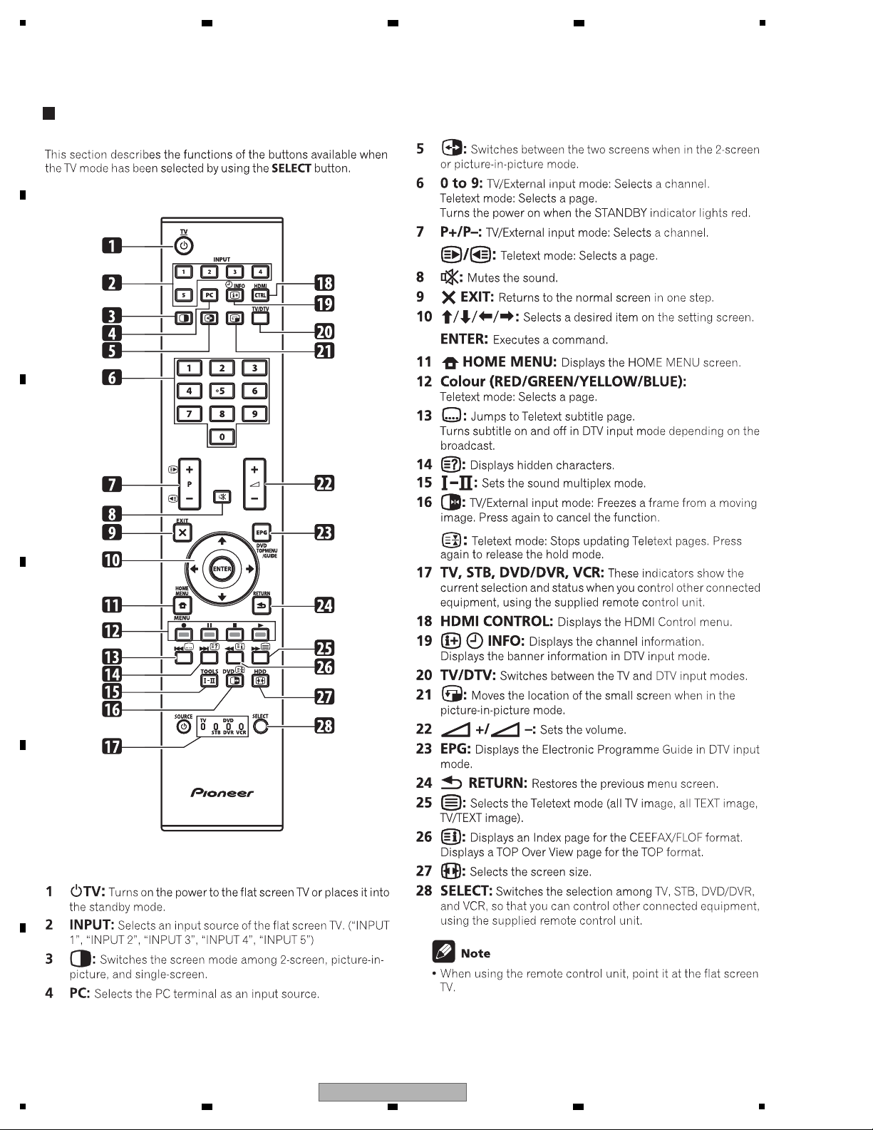
PIONEER CORPORATION
2008
PDP-LX5090
For details, refer to "Important Check Points for good servicing".
FLAT SCREEN TV
PDP-LX5090
THIS MANUAL IS APPLICABLE TO THE FOLLOWING MODEL(S) AND TYPE(S).
Model Type Power Requirement Remarks
PDP-LX5090 WYSIXK5 AC 220 V to 240 V
PDP-LX5090 WYS5 AC 220 V to 240 V
ORDER NO.
ARP3480
T-IZS-001 MAY
2008 Printed in Japan
Page 2

1
This service manual is intended for qualified service technicians ; it is not meant for the casual
do-it-yourselfer. Qualified technicians have the necessary test equipment and tools, and have been
trained to properly and safely repair complex products such as those covered by this manual.
Improperly performed repairs can adversely affect the safety and reliability of the product and may
void the warranty. If you are not qualified to perform the repair of this product properly and safely,
you should not risk trying to do so and refer the repair to a qualified service technician.
WARNING
This product contains lead in solder and certain electrical parts contain chemicals which are known to the state of California to
cause cancer, birth defects or other reproductive harm.
Health & Safety Code Section 25249.6 - Proposition 65
NOTICE
(FOR CANADIAN MODEL ONLY)
Fuse symbols (fast operating fuse) and/or (slow operating fuse) on PCB indicate that replacement parts must
be of identical designation.
REMARQUE
(POUR MODÈLE CANADIEN SEULEMENT)
Les symboles de fusible (fusible de type rapide) et/ou (fusible de type lent) sur CCI indiquent que les pièces
de remplacement doivent avoir la même désignation.
SAFETY PRECAUTIONS
NOTICE : Comply with all cautions and safety related notes
located on or inside the cabinet and on the chassis.
The following precautions should be observed :
1. When service is required, even though the PDP UNIT an
isolation transformer should be inserted between the power line
and the set in safety before any service is performed.
2. When replacing a chassis in the set, all the protective devices
must be put back in place, such as barriers, nonmetallic knobs,
adjustment and compartment covershields, isolation resistor capacitor, etc.
3. When service is required, observe the original lead dress. Extra
precaution should be taken to assure correct lead dress in the
high voltage circuitry area.
4. Always use the manufacture's replacement components.
Especially critical components as indicated on the circuit
diagram should not be replaced by other manufacture's.
Furthermore where a short circuit has occurred, replace those
components that indicate evidence of overheating.
5. Before returning a serviced set to the customer, the service
technician must thoroughly test the unit to be certain that it is
completely safe to operate without danger of electrical shock,
and be sure that no protective device built into the set by the
manufacture has become defective, or inadvertently defeated
during servicing. Therefore, the following checks should be
performed for the continued protection of the customer and
servicetechnician.
6. Perform the following precautions against unwanted radiation
and rise in internal temperature.
• Always return the internal wiring to the original styling.
• Attach parts (Gascket, Ferrite Core, Ground, Rear Cover,
Shield Case etc.) surely after disassembly.
7. Perform the following precautions for the PDP panel.
• When the front case is removed, make sure nothing hits the
panel face, panel corner, and panel edge (so that the glass does
not break).
• Make sure that the panel vent does not break. (Check that the
cover is attached.)
• Handle the FPC connected to the panel carefully.
Twisting or pulling the FPC when connecting it to the
connector will cause it to peel off from the panel.
8. Pay attention to the following.
• Pay extreme caution when the front case and rear panel are
removed because this may cause a high risk of disturbance to
TVs and radios in the surrounding.
2 3 4
SAFETY INFORMATION
A
B
C
D
E
F
2
1
2 3 4
PDP-LX5090
Page 3
5
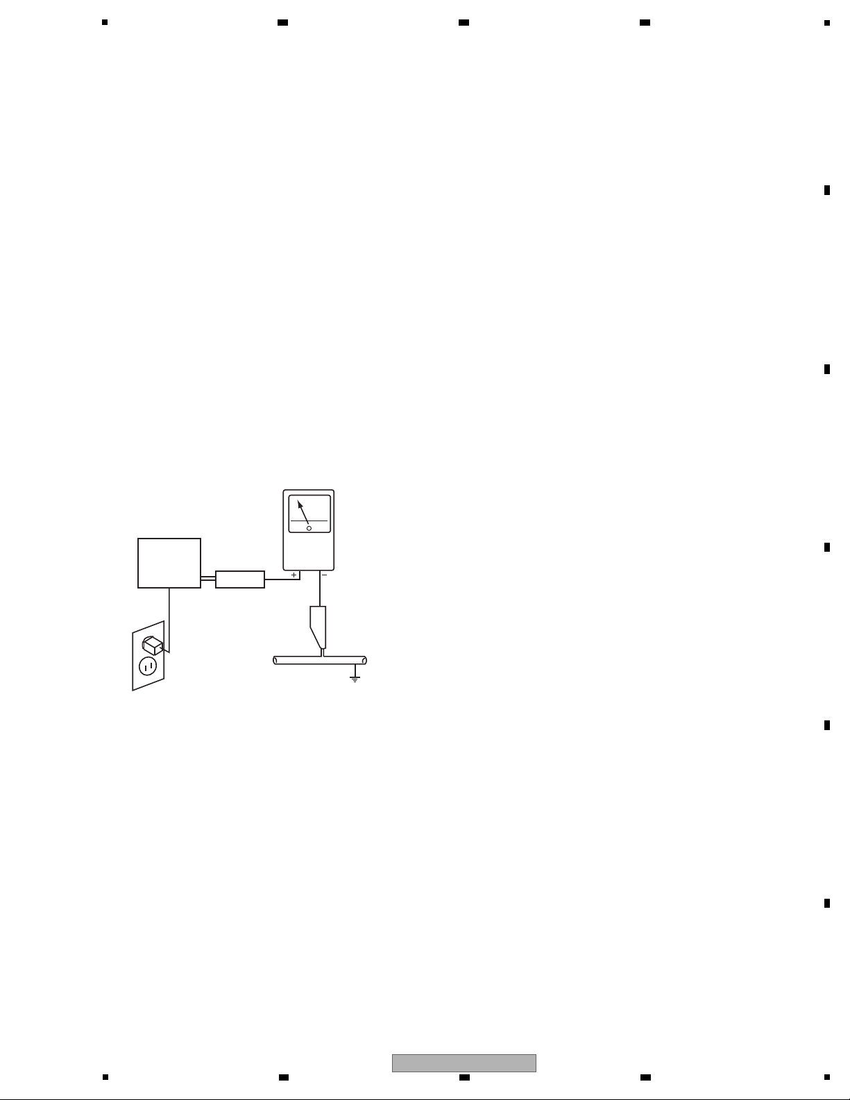
Leakage Current Cold Check
With the AC plug removed from an AC power source, place a
jumper across the two plug prongs. Turn the AC power switch on.
Using an insulation tester (DC 500V), connect one lead to the
jumpered AC plug and touch the other lead to each exposed metal
part (input/output terminals, screwheads, metal overlays, control
shafts, etc.), particularly any exposed metal part having a return
path to the chassis. Exposed metal parts having a return path to
the chassis should have a minimum resistor reading of 4 MΩ.
The below 4 MΩ resistor value indicate an abnormality which
require corrective action. Exposed metal parts not having a return
path to the chassis will indicate an open circuit.
Leakage Current Hot Check
Plug the AC line cord directly into an AC power source (do not
use an isolation transformer for this check).
Turn the AC power switch on.
Using a "Leakage Current Tester (Simpson Model 229
equivalent)", measure for current from all exposed metal parts of
the cabinet (input/output terminals, screwheads, metal overlays,
control shaft, etc.), particularly any exposed metal part having a
return path to the chassis, to a known earth ground (water pipe,
conduit, etc.). Any current measured must not exceed 1 mA.
ANY MEASUREMENTS NOT WITHIN THE LIMITS
OUTLINED ABOVE ARE INDICATIVE OF A POTENTIAL
SHOCK HAZARD AND MUST BE CORRECTED BEFORE
RETURNING THE SET TO THE CUSTOMER.
PRODUCT SAFETY NOTICE
Many electrical and mechanical parts in PIONEER set have
special safety related characteristics. These are often not evident
from visual inspection nor the protection afforded by them
necessarily can be obtained by using replacement components
rated for higher voltage, wattage, etc. Replacement parts which
have these special safety characteristics are identified in this
Service Manual.
Electrical components having such features are identified by
marking with a > on the schematics and on the parts list in this
Service Manual.
The use of a substitute replacement component which dose not
have the same safety characteristics as the PIONEER
recommended replacement one, shown in the parts list in this
Service Manual, may create shock, fire or other hazards.
Product Safety is continuously under review and new instructions
are issued from time to time. For the latest information, always
consult the current PIONEER Service Manual. A subscription to,
or additional copies of, PIONEER Service Manual may be
obtained at a nominal charge from PIONEER.
Leakage
current
tester
Reading should
not be above
1 mA
Device
under
test
Test all
exposed metal
surfaces
Also test with
plug reversed
(Using AC adapter
plug as required)
Earth
ground
AC Leakage Test
6 7 8
A
B
C
D
E
F
PDP-LX5090
5
6 7 8
3
Page 4
1
[Important Check Points for Good Servicing]
In this manual, procedures that must be performed during repairs are marked with the below symbol.
Please be sure to confirm and follow these procedures.
1. Product safety
Please conform to product regulations (such as safety and radiation regulations), and maintain a safe servicing environment by
following the safety instructions described in this manual.
1 Use specified parts for repair.
Use genuine parts. Be sure to use important parts for safety.
2 Do not perform modifications without proper instructions.
Please follow the specified safety methods when modification(addition/change of parts) is required due to interferences such as
radio/TV interference and foreign noise.
3 Make sure the soldering of repaired locations is properly performed.
When you solder while repairing, please be sure that there are no cold solder and other debris.
Soldering should be finished with the proper quantity. (Refer to the example)
4 Make sure the screws are tightly fastened.
Please be sure that all screws are fastened, and that there are no loose screws.
5 Make sure each connectors are correctly inserted.
Please be sure that all connectors are inserted, and that there are no imperfect insertion.
6 Make sure the wiring cables are set to their original state.
Please replace the wiring and cables to the original state after repairs.
In addition, be sure that there are no pinched wires, etc.
7 Make sure screws and soldering scraps do not remain inside the product.
Please check that neither solder debris nor screws remain inside the product.
8 There should be no semi-broken wires, scratches, melting, etc. on the coating of the power cord.
Damaged power cords may lead to fire accidents, so please be sure that there are no damages.
If you find a damaged power cord, please exchange it with a suitable one.
9 There should be no spark traces or similar marks on the power plug.
When spark traces or similar marks are found on the power supply plug, please check the connection and advise on secure
connections and suitable usage. Please exchange the power cord if necessary.
a Safe environment should be secured during servicing.
When you perform repairs, please pay attention to static electricity, furniture, household articles, etc. in order to prevent injuries.
Please pay attention to your surroundings and repair safely.
2. Adjustments
To keep the original performance of the products, optimum adjustments and confirmation of characteristics within specification.
Adjustments should be performed in accordance with the procedures/instructions described in this manual.
4. Cleaning
For parts that require cleaning, such as optical pickups, tape deck heads, lenses and mirrors used in projection monitors, proper
cleaning should be performed to restore their performances.
3. Lubricants, Glues, and Replacement parts
Use grease and adhesives that are equal to the specified substance.
Make sure the proper amount is applied.
5. Shipping mode and Shipping screws
To protect products from damages or failures during transit, the shipping mode should be set or the shipping screws should be
installed before shipment. Please be sure to follow this method especially if it is specified in this manual.
A
2 3 4
B
C
D
E
F
4
1
PDP-LX5090
2 3 4
Page 5

5
6 7 8
CONTENTS
SAFETY INFORMATION.......................................................................................................................................................... 2
1. SERVICE PRECAUTIONS.................................................................................................................................................... 6
1.1 NOTES ON SOLDERING ...............................................................................................................................................6
1.2 CHARGED SECTION AND HIGH VOLTAGE GENERATING POINT .............................................................................7
2. SPECIFICATIONS ................................................................................................................................................................. 8
2.1 ACCESSORIES.............................................................................................................................................................. 8
2.2 SPECIFICATIONS .......................................................................................................................................................... 9
2.3 PANEL FACILITIES....................................................................................................................................................... 10
3. BASIC ITEMS FOR SERVICE ............................................................................................................................................13
3.1 CHECK POINTS AFTER SERVICING ......................................................................................................................... 13
3.2 QUICK REFERENCE ...................................................................................................................................................14
3.3 PCB LOCATIONS ......................................................................................................................................................... 16
4. BLOCK DIAGRAM .............................................................................................................................................................. 18
4.1 OVERALL WIRING DIAGRAM (1/2)............................................................................................................................. 18
4.2 OVERALL WIRING DIAGRAM (2/2)............................................................................................................................. 20
4.3 OVERALL BLOCK DIAGRAM (1/2) ..............................................................................................................................22
4.4 OVERALL BLOCK DIAGRAM (2/2) ..............................................................................................................................24
4.5 POWER SUPPLY UNIT ................................................................................................................................................ 26
4.6 50F X DRIVE ASSY......................................................................................................................................................28
4.7 50F Y DRIVE, 50F SCAN A and B ASSYS ..................................................................................................................29
4.8 POWER SUPPLY BLOCK of 50F X, Y DRIVE and 50F SCAN A and B ASSYS ......................................................... 30
4.9 50F ADDRESS L and S ASSYS................................................................................................................................... 31
4.10 50F DIGITAL ASSY ....................................................................................................................................................32
4.11 POWER SUPPLY BLOCK of MAIN ASSY.................................................................................................................. 34
4.12 IO_AUDIO ASSY ........................................................................................................................................................36
4.13 LED and IR ASSYS .................................................................................................................................................... 38
5. DIAGNOSIS ........................................................................................................................................................................ 39
5.1 POWER SUPPLY OPERATION ....................................................................................................................................39
5.2 DIAGNOSIS FLOWCHART OF FAILURE ANALYSIS .................................................................................................. 45
5.3 DIAGNOSIS OF PD (POWER-DOWN)......................................................................................................................... 66
5.4 DIAGNOSIS OF SD (SHUTDOWN) ............................................................................................................................. 70
5.5 NON-FAILURE INFORMATION ....................................................................................................................................74
5.6 OUTLINE OF THE OPERATION ..................................................................................................................................76
5.7 OUTLINE OF RS-232C COMMAND ............................................................................................................................ 81
5.8 LIST OF RS-232C COMMANDS ..................................................................................................................................82
5.9 DETAILS OF EACH COMMANDS ................................................................................................................................ 91
6. SERVICE FACTORY MODE ............................................................................................................................................. 105
6.1 OUTLINE OF THE SERVICE FACTORY MODE ........................................................................................................ 105
6.2 DETAILS OF FACTORY MENU ..................................................................................................................................113
7. DISASSEMBLY ................................................................................................................................................................. 137
7.1 FLOWCHART OF REMOVAL ORDER .......................................................................................................................137
7.2 DISASSEMBLY........................................................................................................................................................... 138
8. EACH SETTING AND ADJUSTMENT .............................................................................................................................. 147
8.1 ADJUSTMENT REQUIRED WHEN THE UNIT IS REPAIRED OR REPLACED........................................................ 147
8.2 BACKUP OF THE EEPROM (DIGITAL ASSY) ........................................................................................................... 150
8.3 HOW TO CLEAR HISTORY DATA .............................................................................................................................. 153
8.4 ADJUSTMENT WHEN THE SERVICE PANEL ASSY IS REPLACED .......................................................................154
8.5 ADJUSTMENT WHEN THE DRIVE ASSYS ARE REPLACED.................................................................................. 165
8.6 ADJUSTMENT WHEN THE MAIN OR IO_AUDIO ASSY IS REPLACED.................................................................. 168
9. EXPLODED VIEWS AND PARTS LIST............................................................................................................................. 170
9.1 PACKING SECTION ...................................................................................................................................................170
9.2 REAR SECTION......................................................................................................................................................... 172
9.3 FRONT SECTION ...............................................................................................................
9.4 CHASSIS SECTION (1/2)........................................................................................................................................... 176
9.5 CHASSIS SECTION (2/2)........................................................................................................................................... 178
9.6 PANEL CHASSIS SECTION.......................................................................................................................................180
9.7 MULTIBASE SECTION............................................................................................................................................... 182
9.8 PDP SERVICE ASSY ................................................................................................................................................. 184
.......................................174
A
B
C
D
E
F
PDP-LX5090
5
6 7 8
5
Page 6

1
• For environmental protection, lead-free solder is used on the printed circuit boards mounted in this unit.
Be sure to use lead-free solder and a soldering iron that can meet specifications for use with lead-free solders for repairs
accompanied by reworking of soldering.
• Compared with conventional eutectic solders, lead-free solders have higher melting points, by approximately 40 ºC.
Therefore, for lead-free soldering, the tip temperature of a soldering iron must be set to around 373 ºC in general, although
the temperature depends on the heat capacity of the PC board on which reworking is required and the weight of the tip of
the soldering iron.
Do NOT use a soldering iron whose tip temperature cannot be controlled.
Compared with eutectic solders, lead-free solders have higher bond strengths but slower wetting times and higher melting
temperatures (hard to melt/easy to harden).
The following lead-free solders are available as service parts:
• Parts numbers of lead-free solder:
GYP1006 1.0 in dia.
GYP1007 0.6 in dia.
GYP1008 0.3 in dia.
2 3 4
1. SERVICE PRECAUTIONS
1.1 NOTES ON SOLDERING
A
B
C
D
E
F
6
1
2 3 4
PDP-LX5090
Page 7
5
Fig. High Voltage Generating Point (Rear view)
: Part is the High Voltage Generating Points
other than the Charged Section.
50F Y DRIVE Assy
Plate Y POWER SUPPLY Unit 50F X DRIVE Assy Plate X
50F SCAN A Assy50F SCAN B Assy
The places where the commercial AC power is used without
passing through the power supply transformer.
If the places are touched, there is a risk of electric shock. In
addition, the measuring equipment can be damaged if it is
connected to the GND of the charged section and the GND of the
non-charged section while connecting the set directly to the
commercial AC power supply. Therefore, be sure to connect the
set via an insulated transformer and supply the current.
1. Power Cord
2. AC Inlet
3. Power Switch
4. Fuse (In the POWER SUPPLY Unit)
5. STB Transformer and Converter Transformer
(In the POWER SUPPLY Unit)
6. Other primary side of the POWER SUPPLY Unit
AC inlet Power switch
: Part is Charged Section.
Charged Section
The places where voltage is 100 V or more except for the charged
places described above. If the places are touched, there is a risk of
electric shock.
The VSUS voltage remains for several minutes after the power to
the unit is turned off. These places must not be touched until
about 10 minutes after the power is turned off, or it is confirmed
with a tester that there is no residual VSUS voltage.
If the procedures described in “5.6 [1] PANEL DRIVE-POWER
ON/OFF FUNCTION” are performed before the power is turned
off, the voltage will be discharged in about 30 seconds.
50F X DRIVE Assy .......................................................... (205 V)
50F Y DRIVE Assy ......................................... (−280 V to 420 V)
50F SCAN A Assy .......................................... (−280 V to 420 V)
50F SCAN B Assy ........................................... (−280 V to 420 V)
High Voltage Generating Point
6 7 8
1.2 CHARGED SECTION AND HIGH VOLTAGE GENERATING POINT
A
B
C
D
E
F
5
6 7 8
PDP-LX5090
7
Page 8
1
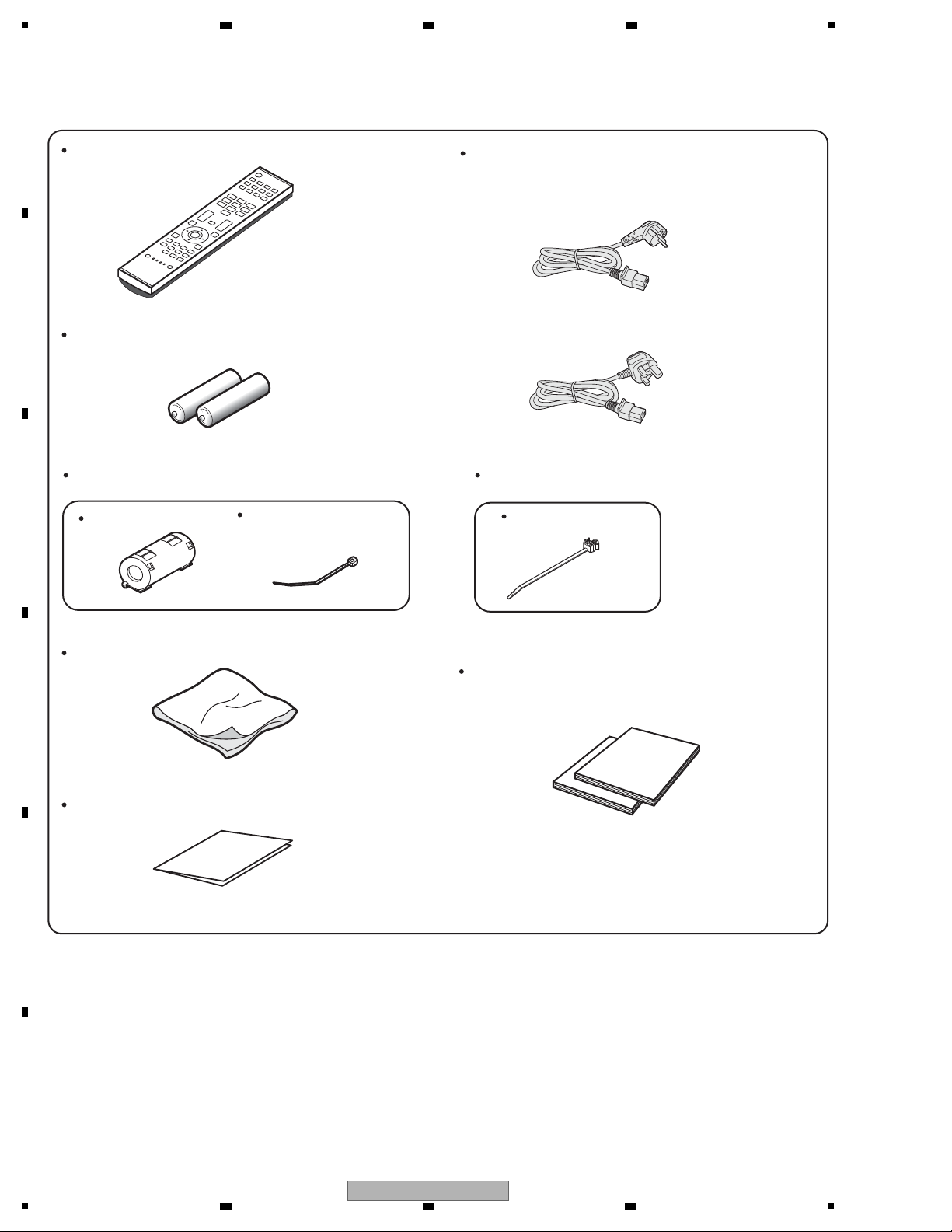
Remote control unit
(AXD1564)
Power cable
Cable tie (for ferrite core)
Cable clamp (×4)
Ferrite core
(ATX1039)
Dry cell battery (R6, AA) (×2)
(for remote control unit)
Ferrite core
Cleaning cloth (AED1285)
Warranty card
Operating instructions (×2)
(ARE1492: WYSIXK5 only)
(ARC1606: WYSIXK5 only) or (ARC1618: WYS5 only)
Binder Assy
(AEC2158)
For Europe, except UK and Republic of Ireland
For UK and Republic of Ireland
Only the power cable appropriate for your country or region
is supplied:
(ADG1214)
(ADG1223: WYSIXK5 only)
2. SPECIFICATIONS
2.1 ACCESSORIES
A
2 3 4
B
C
D
E
F
8
1
2 3 4
PDP-LX5090
Page 9
5
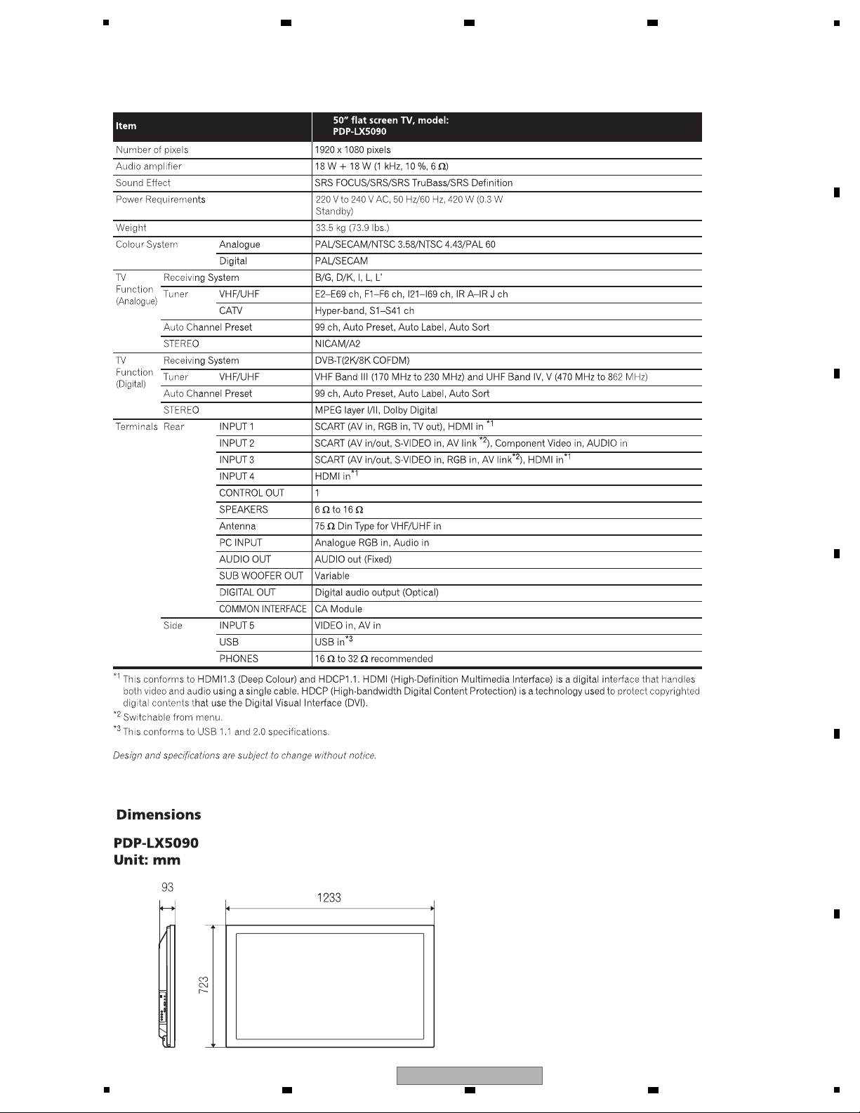
2.2 SPECIFICATIONS
6 7 8
A
B
C
D
E
F
PDP-LX5090
5
6 7 8
9
Page 10
1
Front Section
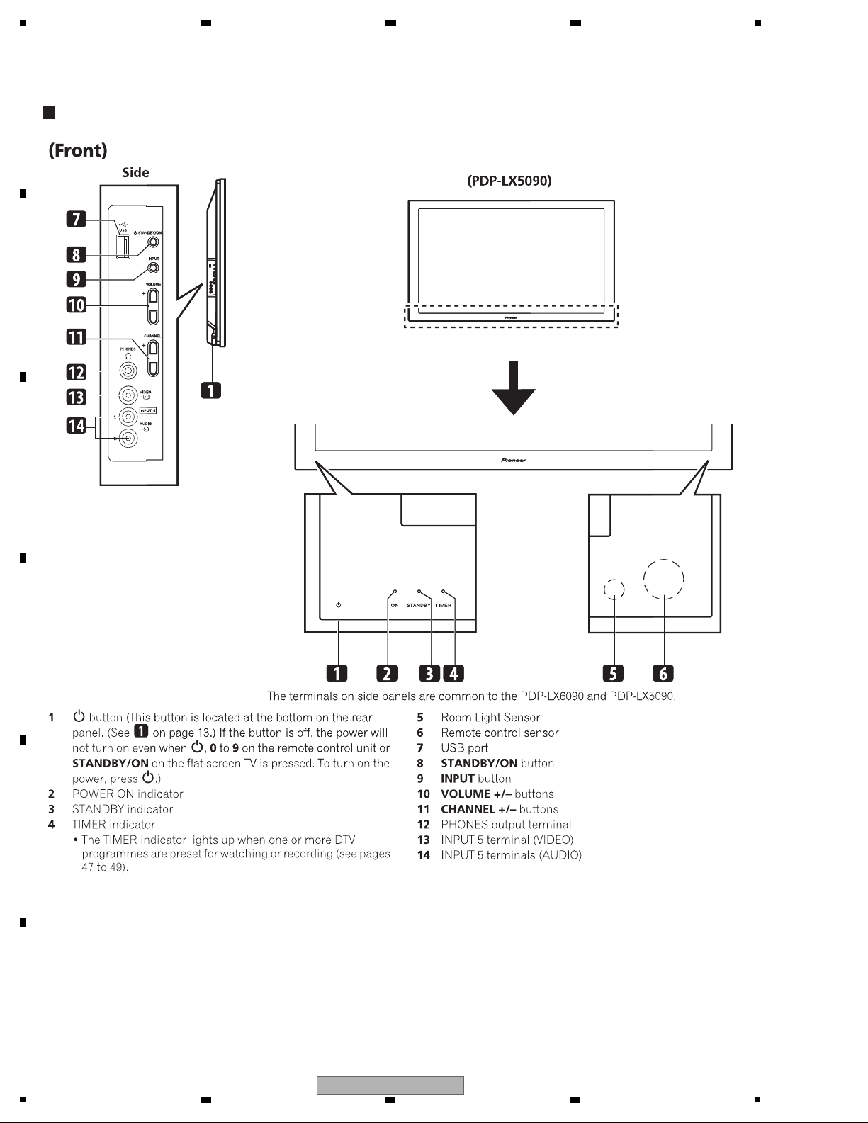
2.3 PANEL FACILITIES
A
B
2 3 4
C
D
E
F
10
1
2 3 4
PDP-LX5090
Page 11
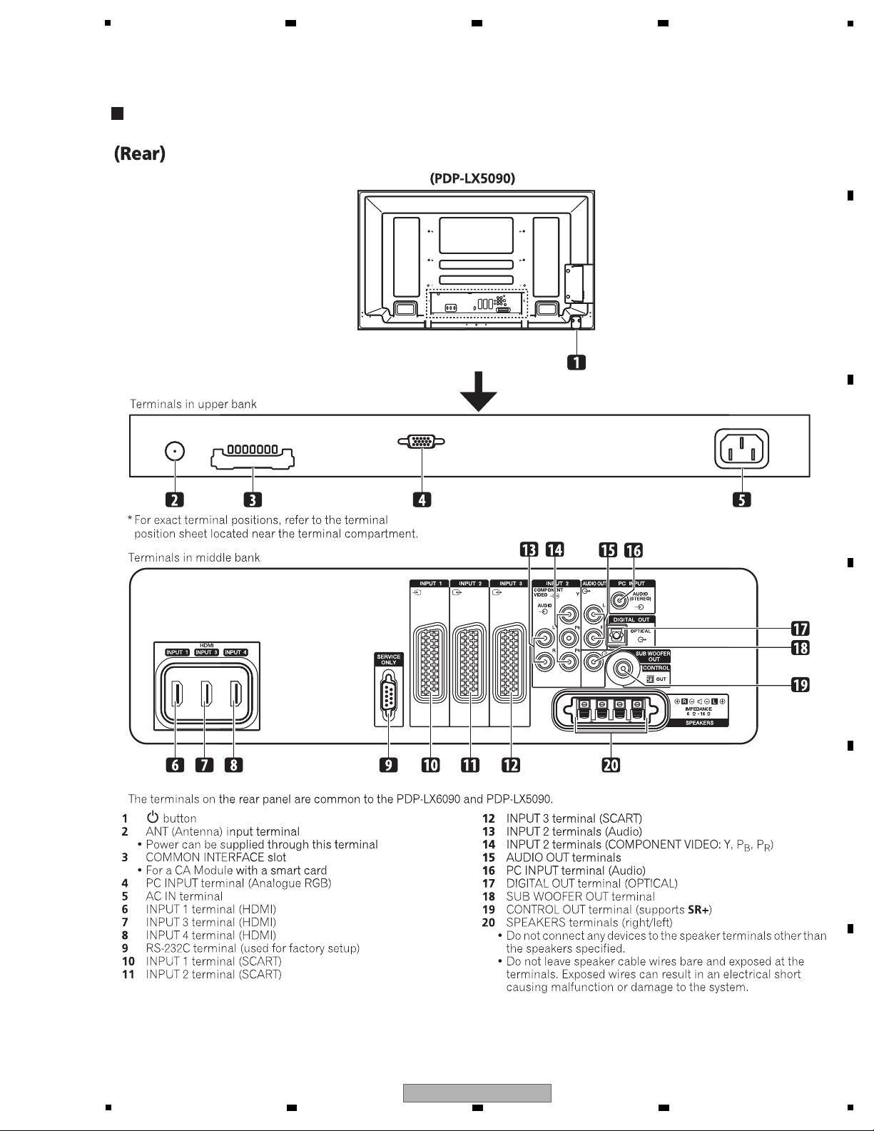
Rear Section
5
6 7 8
A
B
C
D
E
F
PDP-LX5090
5
6 7 8
11
Page 12
1
Remote Control Unit
A
B
2 3 4
C
D
E
F
12
1
2 3 4
PDP-LX5090
Page 13
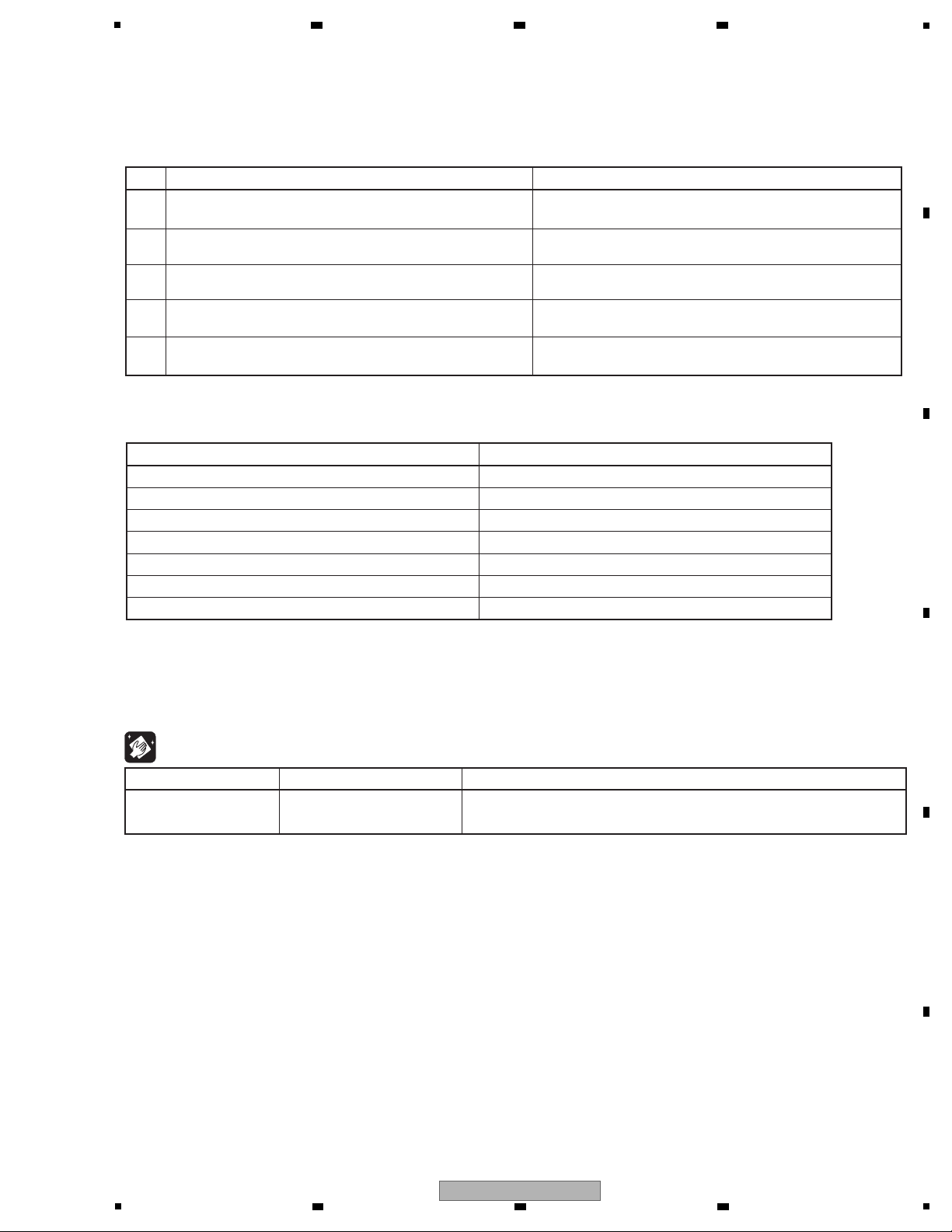
5
Items to be checked after repair (PDP)
To ensure the quality of the product after repair, check the recommended items shown below:
See the table below for the items to be checked regarding video and audio:
Item to be checked regarding video Item to be checked regarding audio
Block noise Distortion
Horizontal noise Noise
Dot noise Volume too low
Disturbed image (video jumpiness) Volume too high
Too dark Volume fluctuating
Too bright Sound interrupted
Mottled color
No. Procedures Item to be checked
1
Check if all the symptoms pointed out by the customer have been
addressed.
The symptoms in question must not be reproduced.
2 Connect the peripheral equipment.
Connect all external peripheral equipment as originally connected
and check if the connections are correct.
3 Check the video and audio.
Tune in to the stations that the customer would normally receive
and check if video and audio are normal.
4 Check the buttons and controls.
Use the buttons and controls on the remote control unit and main
unit and check if they operate properly.
5 Check the cabinet.
Check for any scratches or dirt that have been made or attached
on the cabinet after receiving the product for repair.
Name Part No. Remarks
Used to fan cleaning.
Refer to “9.4 CHASSIS SECTION (1/2)”.
Cleaning paper GED-008
Cleaning
6 7 8
3. BASIC ITEMS FOR SERVICE
3.1 CHECK POINTS AFTER SERVICING
A
B
C
D
E
F
PDP-LX5090
5
6 7 8
13
Page 14
1
Notes when visiting for service
1. Notes when disassembling/reassembling
1 Rear case
When reassembling the rear case, the screws must be tightened in a
specific order. Be careful not to tighten them in the wrong order forcibly.
For details, see "Rear Case" in "7. DISASSEMBLY".
2 Attaching screws for the HDMI connector
When attaching the HDMI connector after replacing the Main Assy,
secure the HDMI connector manually with a screwdriver, but not
with an electric screwdriver. If you tighten the screws too tightly
with an electric screwdriver, the screw heads may be damaged, in
which case the screws cannot be untightened/tightened any more.
2. On parts replacement
1 How to discharge before replacing the Assys
A charge of significant voltage remains in the Plasma Panel even
after the power is turned off. Safely discharge the panel before
replacement of parts, in either manner indicated below:
A:
Let the panel sit at least for 3 minutes after the power is turned off.
B: Turn the Large Signal System off before the power is turned off
then, after 1 minute, turn the power off.
For details, see "5.6 [1] PANEL DRIVE-POWER ON/OFF
FUNCTION".
2 On the settings after replacement of the Assys
Some boards need settings made after replacement of the Assys.
For details, see "8. EACH SETTING AND ADJUSTMENT".
3. On various settings
1 Setting in Factory mode
After a Mask indication into the panel is performed, be sure to
set the Mask setting to "OFF" then exit Factory mode.
Adjustments and Settings after replacement of the
Assys (Procedures in Factory mode)
1. Digital Video Assy: Transfer of backup data
1 Select {PANEL FACTORY}, {ETC}, then {BACKUP DATA}. (After entering Factory
mode, press [MUTING] once, press [ENTER/SET], press [j] seven times, then
press [ENTER/SET].)
2 Select {TRANSFER}, using [l], then hold [ENTER/SET] pressed for at least 5
seconds.
3 After transfer of backup data is completed, {ETC} is automatically selected, and the
LED on the front panel returns to normal lighting.
2. MAIN Assy: Execution of FINAL SETUP.
1 Select {INITIALIZE} then {FINAL SETUP}, then press [ENTER/SET]. (After entering
Factory mode, press [MUTING] three times, then press [j] four times.)
2 Select "YES", using [l]. Then hold [ENTER/SET] pressed for at least 5 seconds.
3 After "FINAL SETUP IS COMPLETE" is displayed on the screen, turn the POWER
switch of the main unit off.
3. POWER SUPPLY Unit: Clearance of the accumulated power-on count
and maximum temperature value
1 Select {PANEL FACTORY}, {ETC}, then {P COUNT INFO}. (After entering Factory
mode, press [MUTING] once, press [ENTER/SET], press [j] seven times, press
[ENTER/SET], then press [j] six times.)
2 Press [l] to select "CLEAR". Hold [ENTER/SET] pressed for at least 5 seconds.
After clearance is completed, "ETC" is automatically selected. Clear the maximum
temperature value (MAX TEMP) in the same manner.
4. Other Assys: Clearance of the maximum temperature value
1 Select {PANEL FACTORY}, {ETC}, then {MAX TEMP}. (After entering Factory mode,
press [MUTING] once, press [ENTER], press [j] seven times, press [ENTER/SET],
then press [j] seven times.)
2 Press [l] to select "CLEAR". Hold [ENTER/SET] pressed for at least 5 seconds.
After clearance is completed, "ETC" is automatically selected.
How to locate several items on the Factory menu
1. Confirmation of accumulated power-on time and power-on
count
Select {INFORMATION} then {HOUR METER}.
(After entering Factory mode, press [j] four times.)
2. Confirmation of the Power-down and Shutdown histories
1 Panel system
PD: Select {PANEL FACTORY} then {POWER DOWN}.
(After entering Factory mode, press [MUTING] once, press
[ENTER/SET], then press [j] two times.)
SD: Select {PANEL FACTORY} then {SHUT DOWN}.
(After entering Factory mode, press [MUTING] once, press
[ENTER/SET], then press [j] three times.)
2 MTB section
Select {INFORMATION} then {MAIN NG}.
(After entering Factory mode, press [j] two times.)
3. How to display the Mask indication
1 Mask indication in the panel side
1. Select {PANEL FACTORY} then {RASTER MASK SETUP}.
(After entering Factory mode, press [MUTING] once, press
[ENTER/SET], then press [j] 8 times.)
2. Press [ENTER/SET], then select a Mask indication, using [i] or [j].
{ } : Item on the Factory menu
[ ] : Key on the remote control unit
" " : Screen indication
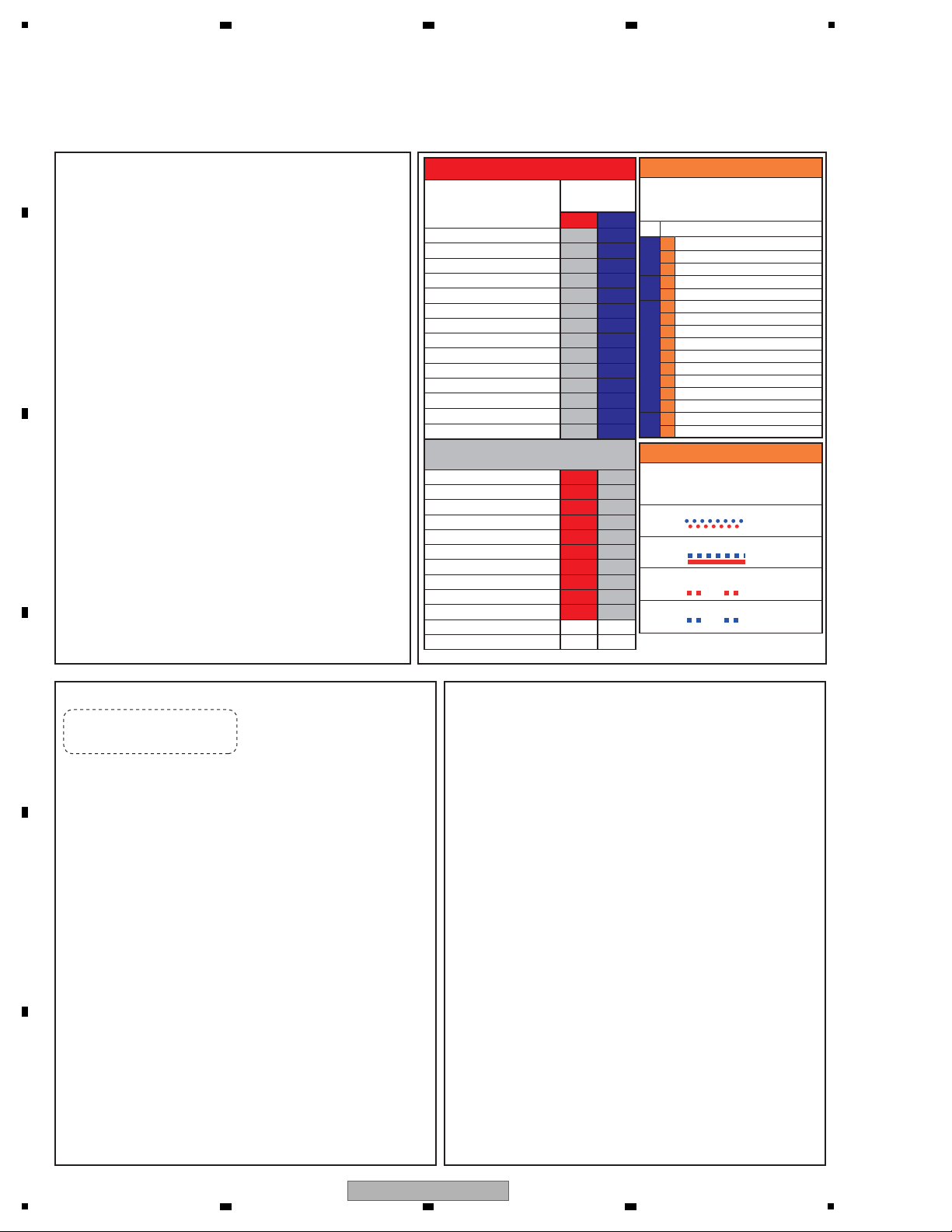
Quick Reference upon Service Visit 1
Notes, PD/SD diagnosis, and methods for various settings
Item
SD SD Subcategory
No. of LEDs
flashing
1 Rewriting software
If the DISPLAY key is pressed during
shutdown, the orange LED flashes.
For indication patterns other than
described below, see 5.4 [2].
2 No backup
LED Display Information
Red 1
Red 2
Red 3
Red 4
Red 6
Red 7
Red 8
Red 10
Red 11
Red 12
Red 15
Blue 1
Blue 2
Blue 3
Blue 4
Blue 5
Blue 6
Blue 7
Blue 8
Blue 9
Blue 10
Blue 11
Blue 12
Blue 13
Blue 15
Red Blue
SQ_LSI
Module device communication
DIGITAL-RST2
Panel temperature
Audio
Module UCOM communication
Main 3-wire serial communication
Main IIC communication
Main UCOM communication
FAN
Unit high temperature
D-TUNER communication
MTB-RST2/RST4
Main EEPROM
Subcategory confirmation procedure
MR POWER
POWER
SCAN
SCN-5V
Y-DCDC
Y- S U S
ADRS
X-DCDC
X-SUS
DIG-DCDC
UNKNOWN
B
R
B
R
B
R
B
R
3 PD (2-15)
4 SD (1-15)
For indication patterns other than
described below, see 5.1 [1].
PD/SD
2
4
8
13
1
2
3
1
2
1
2
3
4
5
6
7
8
13
1
2
EEPROM
BACKUP
DAC
PANEL high temperature
PANEL low temperature
Tuner 1
MSP/MAP
AV Switch
RGB Switch
Main VDEC
VDEC-SDRAM
AD/PLL
HDMI
COFDEM (PDP-LX5090 only)
RST2
RST4
3.2 QUICK REFERENCE
A
2 3 4
B
C
D
E
F
14
PDP-LX5090
1
2 3 4
Page 15
5
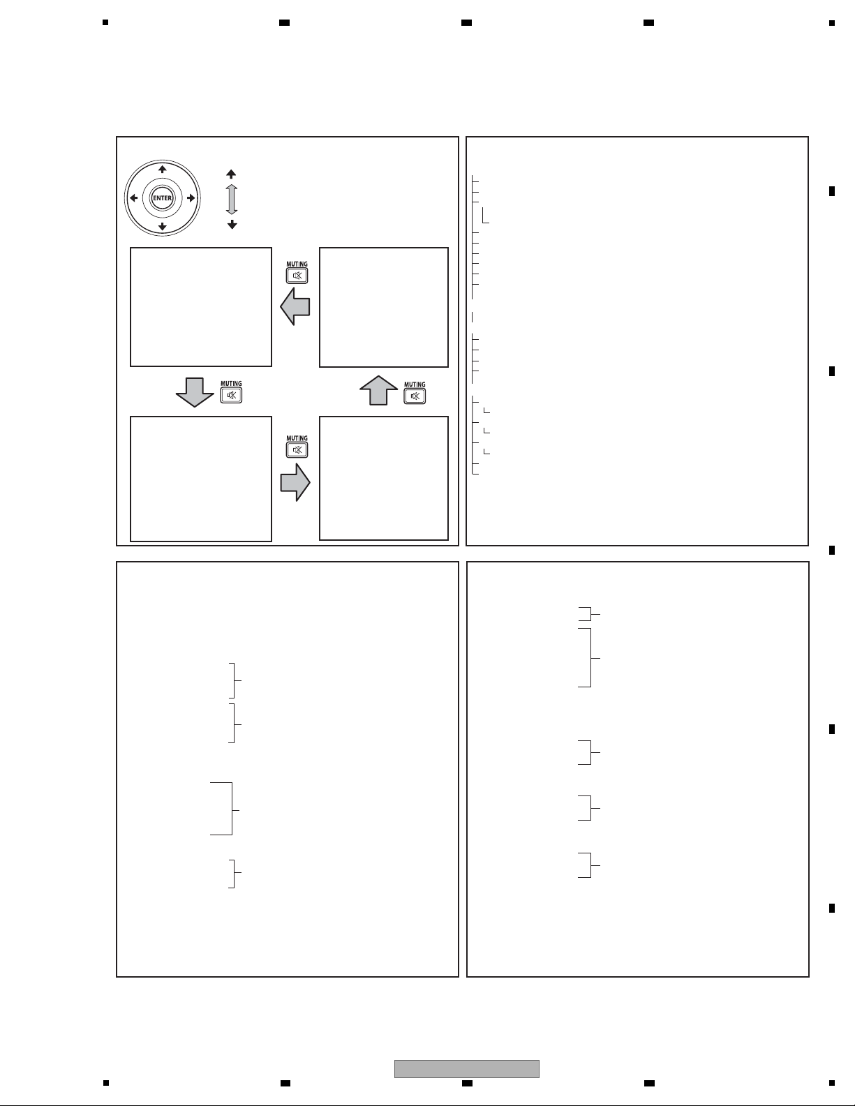
Structure of Layers in Service Factory Mode
INFORMATION mode
1. VERSION (1) The software versions for each microcomputer
2. VERSION (2) The Flash memory versions for each device
3. MAIN NG The shutdown message ID/event times
(Going Clear mode by [ENTER/SET] key)
3-1. CLEAR
Select Yes by [l] key l pushing and hold [ENTER/SET] key
4. TEMPERATURE The temperature/FAN rotating status/Room Light Sensor
5. HOUR METER The HOUR METER/P-COUNT information
6. HDMI SIGNAL INFO 1 The information of HDMI information files
7. HDMI SIGNAL INFO 2 The information of HDMI information files
8. VDEC SIGNAL INFO 1 The signal information of VDEC
9. VDEC SIGNAL INFO 2 The signal information of VDEC
PANEL FACTORY mode Refer to [PANEL FACTORY MODE]
OPTION mode
1. CH PRESET For production line use
2. Digital AFT For production line use (PDP-LX5090H only)
3. SYNC DET For technical analysis
4. CTI For technical analysis
INITIALIZE mode
1. SIDE MASK LEVEL For factory use
1-1. SIDE MASK LEVEL
2. FINAL SETUP Set to Factory default settings (it should perform after
2-1. DATA RESET replacing a MAIN Assy)
3. DTB SERVICE MODE
Information for the Digital Tuner Service Menu is displayed
3-1. MODE SHIFT
4. Wide XGA AUTO For technical analysis
5. AUTO ADJUSTMENT
Quick Reference upon Service Visit 2
Mode transition and structure of layers in Service Factory mode
INFORMATION mode
1. VERSION (1)
2. VERSION (2)
3. MAIN NG
4. TEMPERATURE
5. HOUR METER
6. HDMI SIGNAL INFO 1
7. HDMI SIGNAL INFO 2
8. VDEC SIGNAL INFO 1
9. VDEC SIGNAL INFO 2
PANEL FACTORY mode
1. PANEL INFORMATION
2. PANEL WORKS
3. POWER DOWN
4. SHUT DOWN
5. PANEL-1 ADJ
6. PANEL-2 ADJ
7. PANEL FUNCTION
8. ETC.
9. RASTER MASK SETUP
10. PATTEN MASK SETUP
11. COMBI MASK SETUP
INITIALIZE mode
1. SIDE MASK LEVEL
2. FINAL SETUP
3. DTB SERVICE MENU
4. Wide XGA AUTO
5. AUTO ADJUSTMENT
OPTION mode
1. CH PRESET
2. Digital AFT (*)
3. SYNC DET
4. CTI
(*): PDP-LX5090H only
• To shift to another mode, press [MUTING].
• To shift to another item in a specific mode,
press [i] or [j].
• To shift to the next nested layer below for an
item with a "(+)" indication, press [ENTER/SET].
To return to the next nested layer above,
also press [ENTER/SET].
Mode transition in Service Factory mode
Up
Down
Structure of Layers in Panel Factory Mode 2
8. ETC (+)
1. BACKUP DATA
2. DIGITAL EEPROM
3. PD INFO.
4. SD INFO.
5. HR-MTR INFO.
6. PM/B1-B5
7. P COUNT INFO.
8. MAX TEMP.
9. MIRROR
10. CLS
9. RASTER MASK SETUP (+)
1. MASK OFF
2. RST MASK 01
• • • • •
10. PATTERN MASK SETUP (+)
1. MASK OFF
2. PTN MASK 01
• • • • •
11. COMBI MASK SETUP (+)
1. MASK OFF
2. CMB MASK 01
• • • • •
Structure of Layers in Panel Factory Mode 1
1. PANEL INFORMATION Version indication of the panel
2. PANEL WORKS Indications of the accumulated power-on time and
power-on count of the panel
3. POWER DOWN Indication of the Power-down history
4. SHUT DOWN Indication of the Shutdown history
5. PANEL-1 ADJ (+)
1. VOL SUS
2. VOL OFFSET
• • • • •
10. RESET1ST_KSB
• • • • •
25. SUS FREQ
6. PANEL-2 ADJ (+)
1. R-HIGH
2. G-HIGH
• • • • •
6. B-LOW
7. ABL
7. PANEL FUNCTION (+)
1. R-LEVEL
• • • • •
To "Structure of Layers in Panel Factory Mode 2"
For AM noise prevention (Depending on the mode,
brightness of the screen changes.)
For confirmation of the result of the setting change,
the unit must be turned off then back on again.
Items for factory use
Items for factory use
Settings required after replacement of the panel
For transferring backup data (after replacement of
the DIGITAL Assy)
Change the adjustment status of the DIGITAL Assy.
For use while the Raster Mask is displayed.
Use [i] or [j] to select the type of mask.
Use [l] or [k] to select the sequence.
Switch the Mirror display mode.
Switch the function when checking the color sensor
level.
For use while the Pattern Mask is displayed.
Use [i] or [j] to select the type of mask.
Use [l] or [k] to select the sequence.
For use while the Combination Mask is displayed.
Use [i] or [j] to select the type of mask.
Use [l] or [k] to select the sequence.
For clearance of data for the corresponding items.
The clearing method is the same: Select "CLEAR",
then hold [ENTER/SET] pressed for at least 5
seconds.
For the WB adjustment of the panel and ABL
adjustment.
A setting table is available for each signal frequency.
6 7 8
A
B
C
D
E
F
PDP-LX5090
5
6 7 8
15
Page 16
1
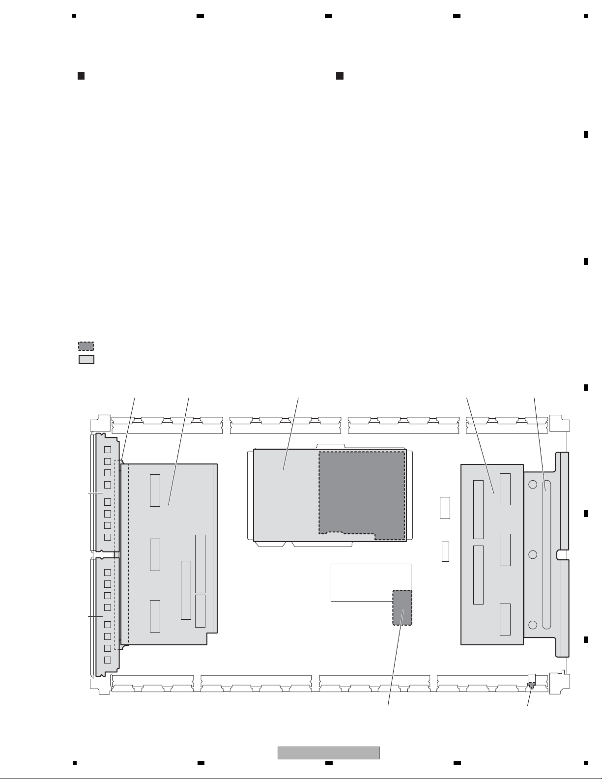
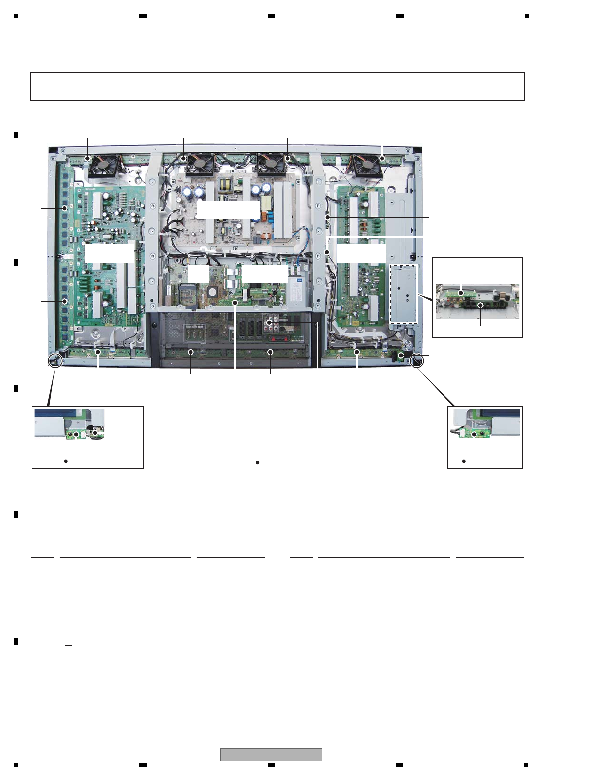
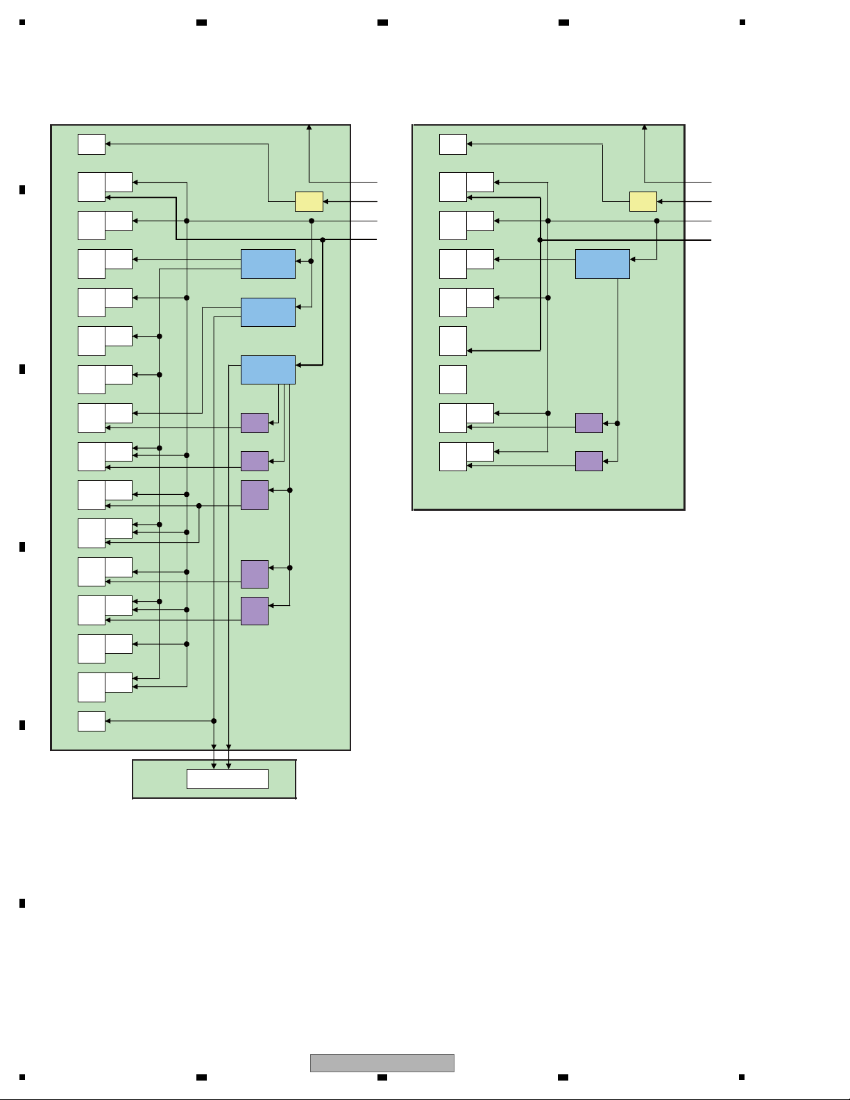
50F Y DRIVE
Assy
MAIN
Assy
50F DIGITAL
Assy
50F X DRIVE
Assy
50F SCAN A Assy
50F ADDRESS L
Assy
50F ADDRESS S
Assy
RLS Assy
IR Assy
50F ADDRESS L
Assy
50F ADDRESS L
Assy
PC Assy IO_AUDIO Assy
50F ADDRESS L
Assy
50F ADDRESS L
Assy
50F ADDRESS L
Assy
50F ADDRESS S
Assy
SIDE IO
Assy
SIDE KEY Assy
LED Assy
FAN CONNECT Assy
POWER SW Assy
SENSOR Assy
50F SCAN B Assy
POWER SUPPLY
Unit
Mark No. Description Part No.
LIST OF ASSEMBLIES
NSP 50F ADDRESS L ASSY AWW1348
NSP 50F ADDRESS S ASSY AWW1349
NSP 50F SCAN A ASSY AWW1350
IC2801 - IC2808 AN16184A
NSP 50F SCAN B ASSY AWW1351
IC2901 - IC2908 AN16184A
SENSOR ASSY AWW1340
50F DIGITAL Assy AWW1347
50F X DRIVE ASSY AWV2546
50F Y DRIVE ASSY AWV2547
Mark No. Description Part No.
> MAIN ASSY AWV2555
IO_AUDIO ASSY AWW1354
SIDE IO ASSY AWW1358
PC ASSY AWW1359
SIDE KEY ASSY AWW1361
LED ASSY AWW1362
IR ASSY AWW1363
FAN CONNECT ASSY AWW1364
RLS ASSY AWW1365
POWER SW ASSY AWW1366
> POWER SUPPLY UNIT AXY1200
PDP SERVICE ASSY 509FE AWU1342
Rear view
Front view Front view
NOTES: - Parts marked by “NSP” are generally unavailable because they are not in our Master Spare Parts List.
-
The > mark found on some component parts indicates the importance of the safety factor of the part.
Therefore, when replacing, be sure to use parts of identical designation.
Note: The wiring shown in the photo is different from the actual wiring, because the product in the photo is a prototype.
Upon servicing, be sure to restore the original wiring of the unit after repair work.
2 3 4
3.3 PCB LOCATIONS
A
B
C
D
E
F
16
1
2 3 4
PDP-LX5090
Page 17

5
6 7 8
A
B
C
D
E
F
PDP-LX5090
5
6 7 8
17
Page 18
1
2 3 4
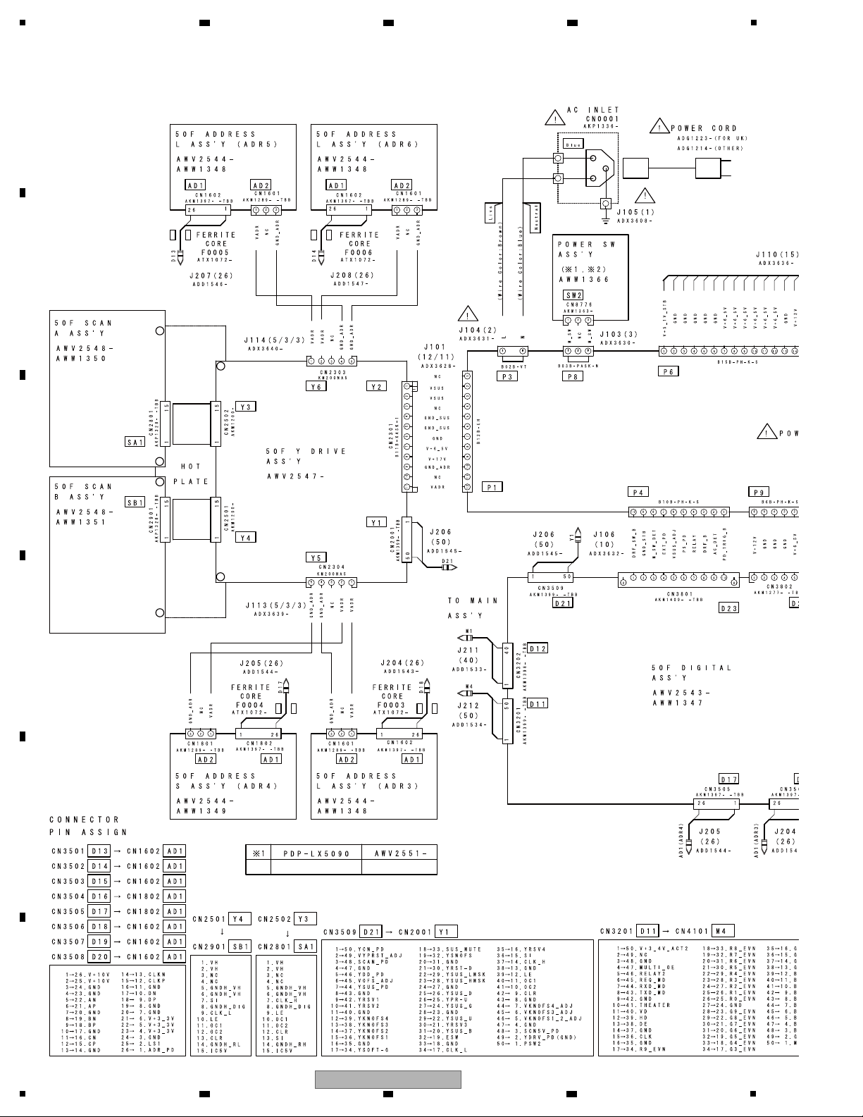
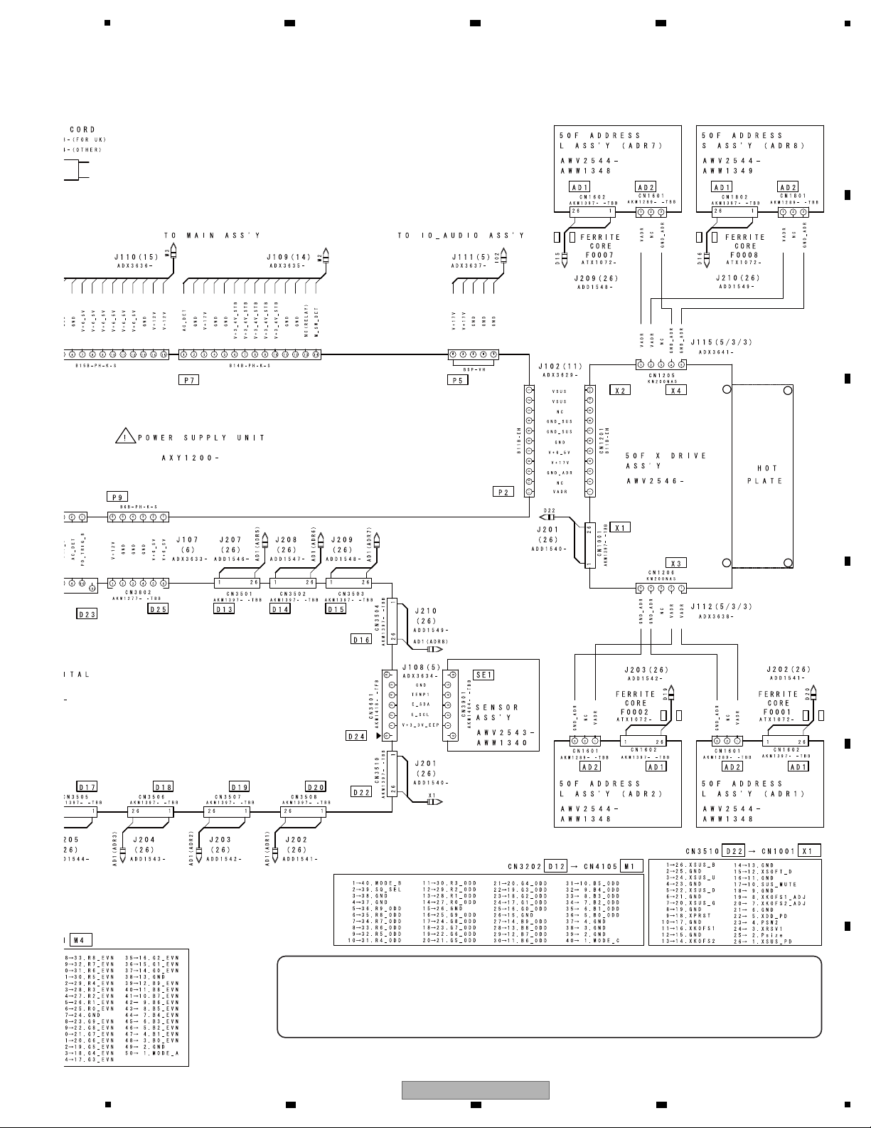
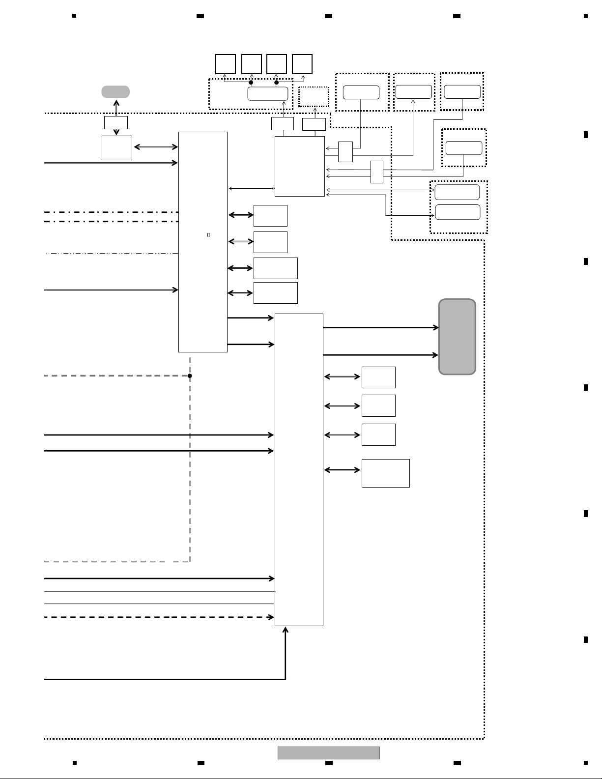
4. BLOCK DIAGRAM
4.1 OVERALL WIRING DIAGRAM (1/2)
A
B
C
D
E
F
18
1
2 3 4
PDP-LX5090
Page 19
5
OVERALL DIAGRAM
PDP-LX5090
k
When ordering service parts, be sure to refer to “EXPLODED VIEWS and PARTS LIST” or
“PCB PARTS LIST”.
k
The > mark found on some component parts indicates the importance of the safety factor
of the part. Therefore, when replacing, be sure to use parts of identical designation.
6 7 8
A
B
C
D
E
PDP-LX5090
5
6 7 8
F
19
Page 20
1
2 3 4
4.2 OVERALL WIRING DIAGRAM (2/2)
A
B
C
D
E
F
20
1
2 3 4
PDP-LX5090
Page 21
5
OVERALL DIAGRAM
PDP-LX5090
6 7 8
A
B
C
D
E
F
PDP-LX5090
5
6 7 8
21
Page 22
1
TE1
D21
OR
V+3_3V_D
MODULE
M30620
LVDS
ADR_PD1
SCAN,YSUS
TEMP1
DAC
UART
SW
V+3V_EEP
ADR_PD
_MSK
SCL,SDA
PULSE
D14
D15
V+1_1V_D
V+1_8V_D
V+2_5V_D
V+3_3V_D
V+1_1V_D
V+2_5V_D
V+2_5V_D V+1_2V_D
V+2_5V_D
V+1_8V_D
D16
D13
MASK
V+12V
V+10V
RELAY1
V+6_5V V+
PSW2
Vsus_AD
Y*****_PD
SCN**_PD
VOFS_ADJ,YPRST_ADJ,
DAC_**
XKOFS*_ADJ
V+3_3V_D
V+10V
V+3_3V_D
V+10V
V+3_3V_D
V+10V
V+3_3V_D
V+10V
SUS_MUTE
V+1_2
V+2_5
V+3_3
D26
UART(CS
DET_CS
D12
SQ_NON
STOP_SQ
YSUS
ADRS_P
V+3VACTV
WE_SQ
ODI_R, G, B
SQ_SEL
RELAY2
MULTI_OE
UART
SCAN B ASSY
(LOW-SIDE)
SCAN A ASSY
(HIGH-SIDE)
SCAN IC
IC2801
SCAN IC
IC2802
SCAN IC
IC2803
SCAN IC
IC2804
SCAN IC
IC2805
SCAN IC
IC2806
SCAN IC
IC2807
SCAN IC
IC2808
SCAN IC
IC2901
SCAN IC
IC2902
SCAN IC
IC2903
SCAN IC
IC2904
SCAN IC
IC2905
SCAN IC
IC2906
SCAN IC
IC2907
SCAN IC
IC2908
WIRE HARNESS
FFC
NOTE:
Y DRIVE ASSY
SENSOR
ASSY
D24
D25
10V
REG.
1.2V
REG.
1.8V
REG.
OR
Pulse
Width
SUB-
XY DRV
PATT
PE
TRAN
PEG
I
DC-DC
CONVERTER
BD8606FV
IC3801
VADR4
V+75V
V+75V
V+10V
V+10V
V+3.3V
V+3.3V
CLK / LE / HBLK
LBLK/R/G/B
CLK / LE / HBLK
LBLK/R/G/B
VADR1
VADR2
VADR3
VDDLS1
VDDLS2
VDDLS3
VADR1
VADR2
VADR3
VDDLS1
VDDLS2
VDDLS3
VDDLS4
AN/P BN/P
CN/ P DN/ P
CLKN/ P
AN/P BN/P
CN/P DN/P
CLKN/P
ADDRESS
S ASSY
ADDRESS L
ASSY
AD2
CN1801
AD2
CN1601
IC1601
LVDS
RECEIVER
RESONANCE
BLOCK
RESONANCE
BLOCK
RESONANCE
BLOCK
RESONANCE
BLOCK
RESONANCE
BLOCK
RESONANCE
BLOCK
RESONANCE
BLOCK
IC1801
LVDS
RECEIVER
AD1
CN1802
AD1
CN1602
VADR1 VADR2
VADR3 VADR4
V+10V
V+75V
V+3.3V
CLK / LE / HBLK
LBLK/R/G/B
VDDLS1 VDDLS2 VDDLS3 VDDLS4
RESONANCE
BLOCK
RESONANCE
BLOCK
RESONANCE
BLOCK
RESONANCE
BLOCK
AN/P BN/P
CN/P DN/P
CLKN/P
ADDRESS L
ASSY
AD2
CN1601
IC1601
LVDS
RECEIVER
AD1
CN1602
VADR1 VADR2
VADR3 VADR4
V+10V
V+75V
V+3.3V
CLK / LE / HBLK
LBLK/R/G/B
VDDLS1 VDDLS2 VDDLS3 VDDLS4
RESONANCE
BLOCK
RESONANCE
BLOCK
RESONANCE
BLOCK
RESONANCE
BLOCK
AN/P BN/P
CN/P DN/P
CLKN/P
ADDRESS L
ASSY
AD2
CN1601
IC1601
LVDS
RECEIVER
AD1
CN1602
VH IC5V
VH IC5V
PSUS
PSUS
VH
IC5V
VH
IC5V
Y3
SA1
SB1
Y4
SCAN SIGNAL
VADR
VSUS
STB5.1V
+6.5V
DRF_SW_B
M_SW_DET
EXT_PD
P2P1
VADR
VSUS
P6
+17V
+6.5V
P5
P9
P7
+6.5V
STB3.4V
+6.5V
+12V
+17V
+12V
+17V
+6.5V
+17V
+12V
M_SW_DET
+17V
AC_DET
VSUS_ADJ
P4
PS_PD
RELAY
DRF_B
AC_DET
PD_TRIG_B
VH IC5V
VH IC5V
VH IC5V
VH IC5V
VH IC5V
VH IC5V
VH IC5V
VH
IC5V
VH IC5V
VH IC5V
VH IC5V
VH IC5V
VH IC5V
VH IC5V
SCAN SIGNAL
VH
VH
IC5V
IC5V
IC202
Q202
SECONDARY
PRIMARY
T702
T901
T501
T101
Y 1
PSUS
PSUS
Scan Signal
IC5V
Y 5
+17V
IC5V/VF
DC/DC
CONV.
IC5V
VC_P
+17V
15V
DC/DC
CONV.
VC_S
VC_U
+5V
Drive Signal
VSUS
VYPRST
VSNOFS
VKNOFS2
VKNOFS3
VKNOFS4
VKNOFS1
MAIN
DC/DC
CONV.
VH
Y 2
Photo Coupler
BLOCK
VSUS
SUS
BLOCK
VSUS
SUS
BLOCK
VSUS
SUS
BLOCK
SUS
PreDrive
+17V
VC_S
H-MSK
VC_S
L-MSK
+17V
KNOFS1
KNOFS3
BLOCK
VKNOFS1
VKNOFS3
RESONANCE
BLOCK
VC_U
+17V
Drive Signal
VC_P
PRST
BLOCK
VYPRST
RST-D
BLOCK
+17V
+17V
KNOFS4
SOFT-G
BLOCK
VC_S
VKNOFS4
+17V
SNOFS
KNOFS2
BLOCK
VSNOFS
VKNOFS2
VC_S
Drive
Signal
SUSOUT
MSK-S
Gate Signal
Y 6
+17V
+5V
VSUS
+6.5V
REG
RESONANCE
BLOCK
VC_U +17V
VADR
VADR
VADR
LOGIC
BLOCK
DRIVER IC
IC1651
DRIVER IC
IC1661
DRIVER IC
IC1671
DRIVER IC
IC1681
DRIVER IC
IC1651
DRIVER IC
IC1661
DRIVER IC
IC1671
DRIVER IC
IC1681
DRIVER IC
IC1651
DRIVER IC
IC1661
DRIVER IC
IC1671
DRIVER IC
IC1681
DRIVER IC
IC1851
DRIVER IC
IC1861
DRIVER IC
IC1871
2 3 4
4.3 OVERALL BLOCK DIAGRAM (1/2)
A
B
C
D
E
F
22
1
PDP-LX5090
2 3 4
Page 23
5
D23
OR
V+6_5
MODULE UCOM
M30620F CSGP
PD
PD_TRG_B,
AC_DET, M_SW_DET
XSUS
LVDS
VDI
AND
AND
AND
DRF_B
RELAY1
DRF_SW_B
PSW1
PSW21
OR
RELAY
RESET
V+3VACTV
RST_SQ
V+3V_D
RST2
SUS_MUT
EVI_R, G, B
KDD
D22
D20
D19D18D17
AND
RESET
THEATE
PS_PD
DRF_B
PSW2
EXT_PD
X****_PD
PSIZE
AND
RESETX
V+1_2V_D
V+2_5V_D
V+3_3V_D
PD_MUTE
ADRS_P
V+3_3V_D
GPIO8
V+3VACTV
EVI_SYNC
RELAY2
MULTI_OE
UART
D11
POWER SUPPLY UNIT
X DRIVE ASSY
POWER SW ASSY
SW2
AC
INLET
DIGITAL
ASSY
D25
Flash Memory
SUB-FILD CONV.
&
XY DRV SEQUENCE
PATTERN GEN.
PEG383B-K
IC3301
LVDS
TRANSMITTER
PEG478A-K
IC3401
DC-DC
CONVERTER
BD8606FV
IC3801
VADR4
V+75V
V+10V
V+3.3V
CLK / LE / HBLK
LBLK/R/G/B
VADR1
VADR2
VADR3
VDDLS1
VDDLS2
VDDLS3
VDDLS4
AN/P BN/P
CN/ P DN/ P
CLKN/ P
ADDRESS L
ASSY
AD2
CN1601
IC1601
LVDS
RECEIVER
RESONANCE
BLOCK
RESONANCE
BLOCK
RESONANCE
BLOCK
RESONANCE
BLOCK
AD1
CN1602
VADR4
V+75V
V+10V
V+3.3V
CLK / LE / HBLK
LBLK/R/G/B
VADR1
VADR2
VADR3
VDDLS1
VDDLS2
VDDLS3
VDDLS4
AN/P BN/P
CN/ P DN/ P
CLKN/ P
ADDRESS L
ASSY
AD2
CN1601
IC1601
LVDS
RECEIVER
RESONANCE
BLOCK
RESONANCE
BLOCK
RESONANCE
BLOCK
RESONANCE
BLOCK
AD1
CN1602
VADR1VADR1 VADR2VADR2
VADR3VADR3 VADR4
V+75V
V+10V
V+10V
V+3.3V
V+75V
V+3.3V
CLK / LE / HBLK
LBLK/R/G/B
CLK / LE / HBLK
LBLK/R/G/B
VDDLS1VDDLS1 VDDLS2VDDLS2 VDDLS3VDDLS3 VDDLS4
RESONANCE
BLOCK
IC1801
LVDS
RECEIVER
RESONANCE
BLOCK
RESONANCE
BLOCK
RESONANCE
BLOCK
RESONANCE
BLOCK
RESONANCE
BLOCK
RESONANCE
BLOCK
AN/P BN/P
CN/P DN/P
CLKN/P
AN/P BN/P
CN/P DN/P
CLKN/P
ADDRESS S
ASSY
ADDRESS L
ASSY
AD2
CN1801
AD2
CN1601
IC1601
LVDS
RECEIVER
AD1
CN1802
AD1
CN1602
F102
+B FOR
RELAY
DRIVE
RY102
D101
PFC Q103
Q104
Q106
D115
D112
D108
IC101
Switching
Switching
Switching
Switching
LIVE
NEUTRAL
+395V
P3
P10
V+3_3V_D
V+10V
V+3_3V_D
V+10V
V+3_3V_D
V+10V
V+3_3V_D
V+10V
PRIMARY
Q502
Q901
Q902
Q704
Q703
Q503
Drive Signal
X 1
PSUS
+17V
OFFSET
BLOCK
VPOFS
VXKOFS1
VXKOFS2
VSUS
SUS
BLOCK
Gate Signal
Drive Signal
RESONANCE
BLOCK
PSUS
+5V
OFFSET
Reg.
Drive Signal
SUS
PreDrive
VPU
+17V
VSUS
SUS
BLOCK
VSUS
SUS
BLOCK
SOFT-D
XPRST
VSUS
+17V
PSUS
LOGIC
BLOCK
+17V
15V
DC/DC
CONV.
VPU
VPOFS
+17V
+5V
VSUS
+6.5V
X 2
REG
X 3
VADR
VADR
VADR
X 4
Gate Signal
Gate Signal
DRIVER IC
IC1651
DRIVER IC
IC1661
DRIVER IC
IC1671
DRIVER IC
IC1681
DRIVER IC
IC1851
DRIVER IC
IC1861
DRIVER IC
IC1871
DRIVER IC
IC1651
DRIVER IC
IC1661
DRIVER IC
IC1671
DRIVER IC
IC1681
DRIVER IC
IC1651
DRIVER IC
IC1661
DRIVER IC
IC1671
DRIVER IC
IC1681
6 7 8
A
B
C
5
6 7 8
PDP-LX5090
D
E
F
23
Page 24
1
Analog Audio signal
Analog Video signal
Digital Video signal
Digital Audio signal
Component signal
Synchronized signal
IF signal
Control signal
Data signal
IO_AUDIO Assy
PC Assy
SIDE IO Assy
MAIN ASSY
JA7701
Input1 SCART
JA7702
Input2 SCART
JA7703
Input3 SCART
JA8601
Input5
CN8602
Head Phone
JA7804
SUB WOOFER
JA7804
Audio Out
JA7802
Audio Input for PC
SPDIF
IC8001
R2S11006FT
(AVSW)
A_TUNER_V
SLOW_SW1/2/3
Y/C
Y/C
SW OUT
HP_L/R OUT
IC8101
R2S11001FT
(RGBSW)
AUDIO_OUT_L/R
L/R IN
PC_L/R IN
IC8201
MSP5651M
(MSP)
IC8401
TAS5122DCA
(D-AMP)
IC4901
SII9125CTU
(HDMI RX)
IC5001
CXB1444R
(HDMI SW)
AIR-SIF
IC4801
AD9985KSTZ
(ADC)
RGB
/YPbPr
IC4702
CM0048BF
(VDEC)
RGB
Main Y/C
Sub Y/C
COMP_Y
IC5701
TC90173FG
(VBI Slicer)
U5301
AXF1192
(Tuner)
CVBS
IC4701
HY57V641620FTP
64Mbit(SDRAM)
FB
CLP
CLP
INPUT3
HDMI
CVBS
SCART1_OUT_V
CVBS
CVBS
JA7881
SPDIF
INPUT4
HDMI
INPUT1
HDMI
CLP,H
CVBS
L/R IN
L/R IN
L/R IN
RAPID_SW1/3
OPT_OUT
AIR OUT L/R
AIR OUT L/R
AIR OUT L/R
SCART2_OUT_V
SCART3_OUT_V
RAPID_SW1
RAPID_SW3
SLOW_SW2
SLOW_SW1
SLOW_SW3
JA7805
INPUT2 Component
Input2 Y/Cb/Cr
Input1 RGB
Input3 RGB
JA7803
Audio Input for
INPUT2 Component
L/R IN
JA8551
SPEAKER TERMINAL
IC5401
DRX3975D
(COFDM)
D_IF1
D_IF2
DT_MON_CVBS
EMMA_DA_GY
PC_RGB
PC_H/V
CN9601
PC Input
SPDIF
I2S
2 3 4
4.4 OVERALL BLOCK DIAGRAM (2/2)
A
B
C
D
E
F
24
1
2 3 4
PDP-LX5090
Page 25
FAN CONNECT ASSY
SIDE KEY ASSY LED ASSY IR ASSY
RLS ASSY
IO_AUDIO ASSY
USB
IC6501
PD6568A
(ARIA)
DIN6 ( 12bit *3 )
DIN4_656DATA ( 8bit )
DIN3_656DATA ( 10bit )
DIN7 OSD 8bit *4
IC6811
AGC1072
(M30620FCSGP)
IF UCOM
IC6702
EDD1232ABBH
128Mbit (DDR)
IC6703
EDD1232ABBH
128Mbit (DDR)
IC6704
EDD1232ABBH
128Mbit (DDR)
IC6701
AGC1079
(S29GL016A90TFIR2)
16Mbit Flash
RDATA
IC7201
K4H510838D
(512Mbit DDR)
IC7204
K4H510838D
(512Mbit DDR)
IC7202
AGC1075
(S29GL064N90TFI04)
(64Mbit FLASH)
IC7205
AGC1076
(S29GL064N90TFI04)
(64Mbit FLASH)
IC5801
M66596FP
INT H/V, EXT H/V
EMMA_DA_GY / BCB / RCR
DIN1_656 ( 8bit )
DIN2 ( 8bit*3 )
RS232C
SR_OUT
IR
REM
SR_OUT
TXD_SR
RXD_SR
TXD_232C
RXD 232C
RLS
M15
CN4208
RLS
KEY1
KEY2
LED
M11
CN4209
KEY
M6
CN4107
RGB 10bit *3
RGB 10bit *3
FAN
M10
CN4201
M5
CN4202
FAN FANFAN
Fan Connect
FAN
RESERVED
IC7003
uPD61123F1
(EMMA SV)
To
DIGITAL
Ass'y
5
6 7 8
A
B
C
D
E
PDP-LX5090
5
6 7 8
F
25
Page 26
1
POWER SUPPLY UNIT
RY102
LIVE
NEUTRAL
PRIMARY
SECONDARY
VADR
VSUS
T901
PFC Q103
Q104
Q106
PS_PD
RELAY
EXT_PD
T702
T501
P3
P2
P1
P6
P5
+6.5V
VSUS_ADJ
Q704
Q703
Switching
Switching
P4
P10
+17V
+17V
+6.5V
+17V
+12V
F102
+B for
RELAY DRIVE
DRF_SW_B
M_SW_DET
PD_TRIG_B
DRF_B
Q902
Q901
Q503
Q502
Switching
Switching
+12V
STB5.1V
+17V
+6.5V
VADR
VSUS
D101
+395V
P9
Switching
+12V
+6.5V
+17V
D108
T101
P7
Switching
IC101
STB3.4V
D112
Q202
AC_DET
M_SW_DET
IC202
+6.5V
D115
AC_DET
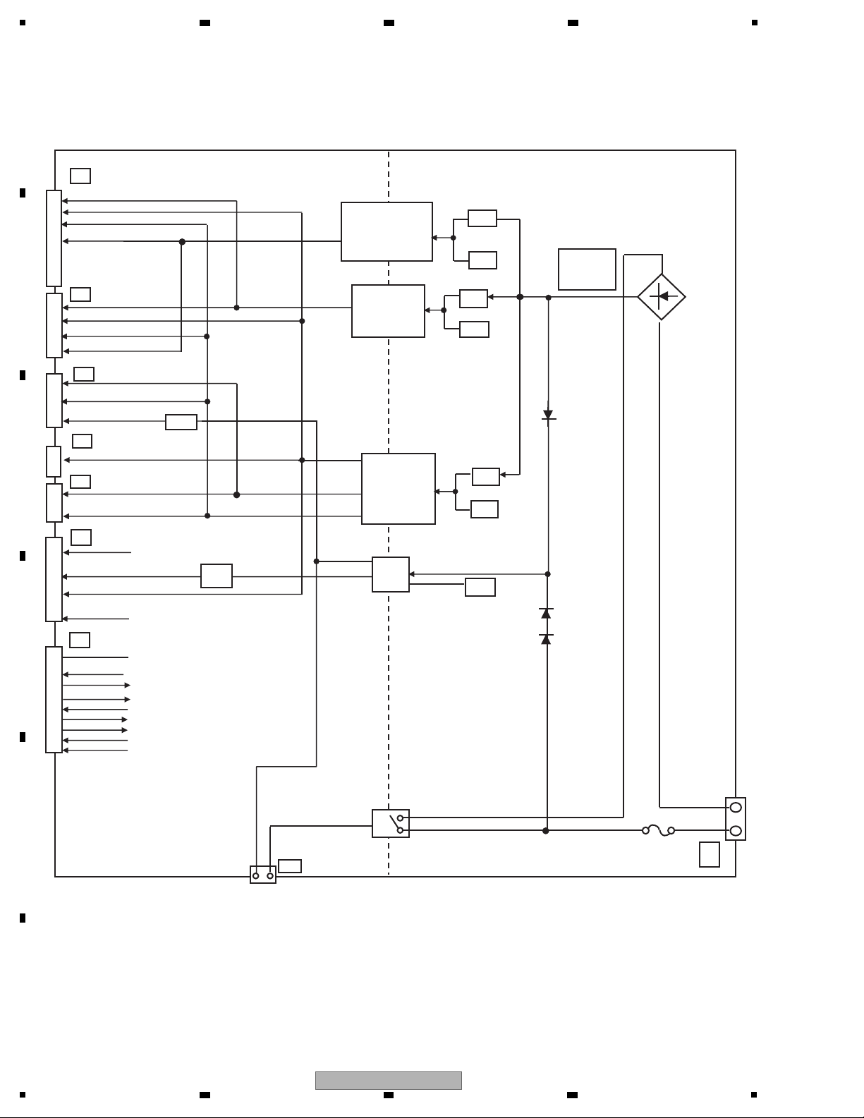
4.5 POWER SUPPLY UNIT
A
2 3 4
B
C
D
E
F
26
1
2 3 4
PDP-LX5090
Page 27

5
6 7 8
A
B
C
D
E
F
PDP-LX5090
5
6 7 8
27
Page 28
1
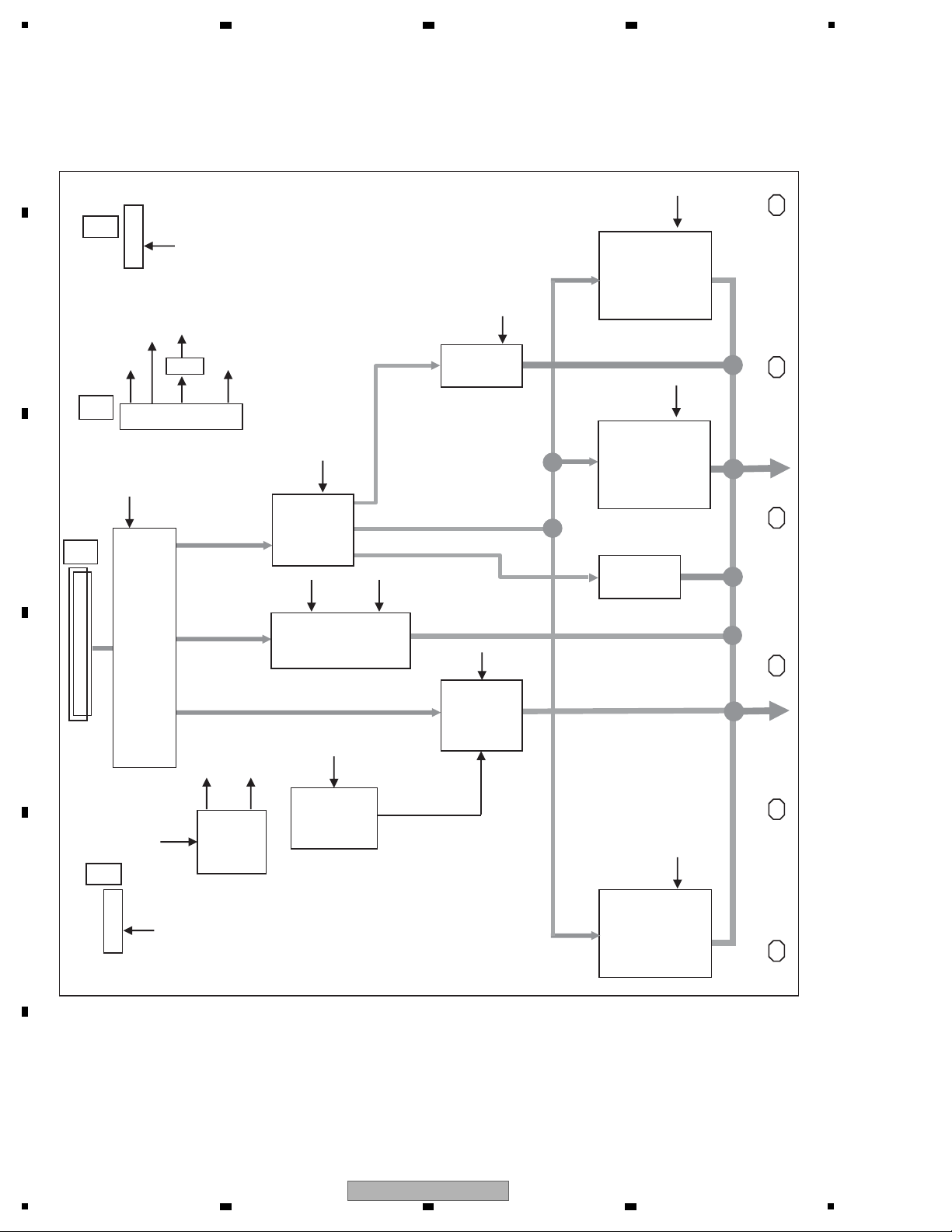
Drive Signal
X 1
PSUS
+17V
OFFSET
BLOCK
VPOFS
VXKOFS1
VXKOFS2
VSUS
SUS
BLOCK
Gate Signal
Gate Signal
Gate Signal
Drive Signal
RESONANCE
BLOCK
PSUS
+5V
OFFSET
Reg.
Drive Signal
SUS
PreDrive
VPU
+17V
VSUS
SUS
BLOCK
VSUS
SUS
BLOCK
SOFT- D
XPRST
VSUS
+17V
PSUS
LOGIC
BLOCK
+17V
15V
DC/DC
CONV.
VPU
VPOFS
+17V
+5V
VSUS
+6.5V
X 2
REG
X 3
VADR
VADR
VADR
X 4
50F X DRIVE ASSY
4.6 50F X DRIVE ASSY
A
2 3 4
B
C
D
E
F
28
1
2 3 4
PDP-LX5090
Page 29
5
50F Y DRIVE ASSY
50F SCAN A ASSY
(HIGH-SIDE)
50F SCAN B ASSY
(LOW-SIDE)
SCAN IC
IC2801
SCAN IC
IC2802
SCAN IC
IC2803
SCAN IC
IC2804
SCAN IC
IC2805
SCAN IC
IC2806
SCAN IC
IC2807
SCAN IC
IC2808
SCAN IC
IC2901
SCAN IC
IC2902
SCAN IC
IC2903
SCAN IC
IC2904
SCAN IC
IC2905
SCAN IC
IC2906
SCAN IC
IC2907
SCAN IC
IC2908
VH IC5V
VH IC5V
PSUS
PSUS
VH
IC5V
VH
IC5V
Y3
SA1
SB1
Y4
SCAN SIGNAL
VH IC5V
VH IC5V
VH IC5V
VH IC5V
VH IC5V
VH IC5V
VH IC5V
VH
IC5V
VH IC5V
VH IC5V
VH IC5V
VH IC5V
VH IC5V
VH IC5V
SCAN SIGNAL
VH
VH
IC5V
IC5V
Y 1
PSUS
PSUS
Scan Signal
IC5V
Y 5
+17V
IC5V/VF
DC/DC
CONV.
IC5V
VC_P
+17V
15V
DC/DC
CONV.
VC_S
VC_U
+5V
Drive Signal
VSUS
VYPRST
VSNOFS
VKNOFS2
VKNOFS3
VKNOFS4
VKNOFS1
MAIN
DC/DC
CONV.
VH
Y 2
Photo Coupler
BLOCK
VSUS
SUS
BLOCK
VSUS
SUS
BLOCK
VSUS
SUS
BLOCK
SUS
PreDrive
+17V
VC_S
H-MSK
VC_S
L-MSK
+17V
KNOFS1
KNOFS3
BLOCK
VKNOFS1
VKNOFS3
RESONANCE
BLOCK
VC_U
+17V
Drive Signal
VC_P
PRST
BLOCK
VYPRST
RST-D
BLOCK
+17V
+17V
KNOFS4
SOFT-G
BLOCK
VC_S
VKNOFS4
+17V
SNOFS
KNOFS2
BLOCK
VSNOFS
VKNOFS2
VC_S
Drive
Signal
SUSOUT
MSK-S
Gate Signal
Y 6
+17V
+5V
VSUS
+6.5V
REG
RESONANCE
BLOCK
VC_U +17V
VADR
VADR
VADR
LOGIC
BLOCK
6 7 8
4.7 50F Y DRIVE, 50F SCAN A and B ASSYS
A
B
C
D
E
5
PDP-LX5090
6 7 8
F
29
Page 30
1
50F X DRIVE ASSY
50F SCAN A, B ASSYS
5.0V
5.0V
Vadr Vadr
5.0V 6.5V 5.0V 6.5V
17V 17V
VSUS VSUS
VC_U VPU
VC_S
VPOFS
VC_P
IC5V
VH
VKOFS1
VKOFS2
IC5V VH
5V
IC5V
DC/DC
Conv.
Scan
Logic
Scan IC
15V
DC/DC
Conv.
HMSK
FET
Pre
drive
Logic
5V
Re
g
.IC
DC/DC
Conv.
SUS-G
IGBT
Pre
drive
SUS-B
IGBT
Pre
drive
SUS-U
IGBT
Pre
drive
SUS-D
IGBT
Pre
drive
XPRST
FET
XSOFT-D
FET
XKOFS1
FET
Pre
drive
XKOFS2
FET
Pre
drive
XKOFS1
Reg.
XKOFS2
Reg.
Logic
SUS-G
IGBT
Pre
drive
SUS-B
IGBT
Pre
drive
SUS-U
IGBT
Pre
drive
SUS-D
IGBT
Pre
drive
LMSK
FET
Pre
drive
YPRST
FET
Pre
drive
SNOFS
FET
Pre
drive
YKOFS
1
FET
Pre
drive
YKOFS
2
FET
Pre
drive
YKOFS
3
FET
Pre
drive
YKOFS
4
FET
Pre
drive
RST-D
FET
Pre
drive
VYKOFS
12
Reg.
VYKOFS
3
Reg.
VYKOFS
4
Reg.
DC/DC
Conv.
VSNOFS
Reg.
VYPRST
Reg.
SOFT-G
FET
Pre
drive
from POWER
SUPPLY
UNT
from POWER
SUPPLY
UNT
to ADDRESS ASSY
to ADDRESS ASSY
Reg.IC
50F Y DRIVE ASSY
Note:
VYPRST, VSNOFS, VYKOFS12, VYKOFS3, VYKOFS4
VXKOFS1 and VXKOFS2 voltages are electrical volume controls.
2 3 4
4.8 POWER SUPPLY BLOCK of 50F X, Y DRIVE and 50F SCAN A and B ASSYS
A
B
C
D
E
F
30
1
2 3 4
PDP-LX5090
Page 31

5
DRIVER IC
IC1651
DRIVER IC
IC1661
DRIVER IC
IC1871
DRIVER IC
IC1861
DRIVER IC
IC1851
DRIVER IC
IC1671
DRIVER IC
IC1681
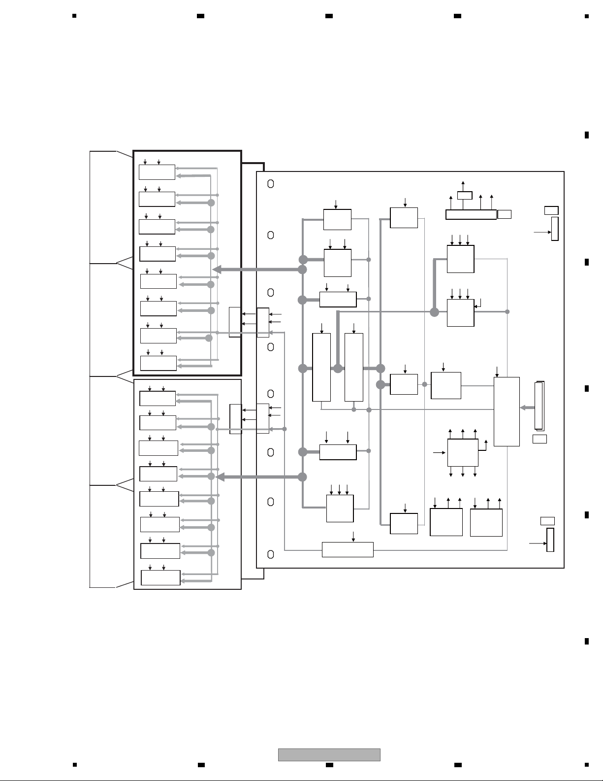
50F ADDRESS S ASSY
50F ADDRESS L ASSY
VADR1
VADR1
VADR2
VADR2
VADR3
VADR3 VADR4
V+75V
V+10V
V+10V
V+3.3V
V+75V
V+3.3V
CLK / LE / HBLK
LBLK/R/G/B
CLK / LE / HBLK
LBLK/R/G/B
VDDLS1
VDDLS1
VDDLS2
VDDLS2
VDDLS3
VDDLS3 VDDLS4
RESONANCE
BLOCK
IC1801
LVDS
RECEIVER
RESONANCE
BLOCK
RESONANCE
BLOCK
RESONANCE
BLOCK
RESONANCE
BLOCK
RESONANCE
BLOCK
RESONANCE
BLOCK
AN/P BN/P
CN/P DN/P
CLKN/P
AN/P BN/P
CN/P DN/P
CLKN/P
AD2
CN1801
AD1
CN1802
AD2
CN1601
AD1
CN1602
IC1601
LVDS
RECEIVER
4.9 50F ADDRESS L and S ASSYS
6 7 8
A
B
C
5
PDP-LX5090
6 7 8
D
E
F
31
Page 32

1
50F DIGITAL ASSY
D23
D21
V+6_5V
V+3_3V_D
OR
D13
LVDS
ADR_PD1
Y*****_PD
SCN**_PD
PS_PD
PD_MUTE
PD
Vsus_AD
PD_TRG_B,
AC_DET,
M_SW_DE
XSUS
SCAN,YSUS
ODI_R, G, B
D11
TEMP1
PSIZE
LVDS
DAC
DAC_**
D24
THEATER
Pulse
Width
SQ_NON
VOFS_ADJ,YPRST_ADJ,
YKNOFS**_ADJ
VDI
V+3VACTV
UART
V+3V_EEP
ADR_PD_MSK
STOP_SQ
AND
DRF_
SCL,SDA
MULTI_OE
DRF_SW_B
PSW1
X****_PD
PSW2
MASK
ADRS_PD
V+6_5V
XKOFS*_ADJ
OR
RELAY
RELAY2
SQ_SEL
V+3VACT
V+3VACT
RESET
RST_SQ
V+3V_D
EXT_PD
RST2
SUS_MUTE
EVI_R, G, B
EVI_SYNC
DRF_B
KDD
D14
D15
D16
D22
D18
D19
D20
D17
RESETX
AND
V+1_1V_D
V+2_5V_D
V+2_5V_D V+1_2V_D
V+2_5V_D
V+1_8V_D
D26
V+3_3V_D
10V
REG
1.2V
REG
1.8V
REG
V+12V V+10V
UART(CS)
YSUS
DET_CS
D12
WE_SQ
RELAY1
SUS_MUTE
AND
AND
GPIO8
PSW2
V+3_3V_D
V+10V
V+3_3V_D
V+10V
V+3_3V_D
V+10V
V+3_3V_D
V+10V
V+3_3V_D
V+10V
V+3_3V_D
V+10V
V+3_3V_D
V+10V
V+3_3V_D
V+10V
RELAY1
D25
V+12V
UART
SUB-FILD CONV.
&
XY DRV SEQUENCE
PATTERN GEN.
PEG383B-K
IC3301
Flash Memory
IC3302
V+1_1V_D
V+1_8V_D
V+2_5V_D
V+3_3V_D
V+3_3V_D
V+1_2V_D
V+2_5V_D
LVDS
TRANSMITTER
PEG478A-K
IC3401
MODULE UCOM
M30620FCSGP
IC3601
RESET
Pulse
Width
O
R
AND
DC-DC
CONVERTER
BD8606FV
IC3801
4.10 50F DIGITAL ASSY
A
B
C
D
2 3 4
E
F
32
1
2 3 4
PDP-LX5090
Page 33

5
6 7 8
A
B
C
D
E
F
PDP-LX5090
5
6 7 8
33
Page 34

1
for DVB-T TUNER
for FAN
V+5_1V_D
V+2_6V_D2
V+2_6V_D2_ARIA
V+VDDIO_ARIA for ARIA
V+2_6V_D2_ARIA_DDR_A
V+2_6V_D2_ARIA_DDR_B
for ARIA_DDR
V+2_6V_D2_ARIA_DDR_C
V+1_2V_D2
V+1_2V_D2_ARIA
V+1_2V_D2_ARIA_PLL1
V+1_2V_D2_ARIA_PLL2
for ARIA
V+1_2V_D2_ARIA_PLL3
V+1_2V_D2_ARIA_PLL4
V+3_4V_STB_IF
V+1_8V_D_COF
for COFDM
V+3_4V_D3_VDEC_RAM
for VDEC
V+3_4V_D3_VDEC
V+3_4V_D3_ARIA
for ARIA
V+3_4V_D4_HDMI
V+3_4V_D4_HDMI_IO
for HDMIRx
V+3_4V_D4_HDMI_A
V+3_4V_D4_HDMI_REG
V+3_4V_D4_HDMISW
for HDMISW
V+1_8V_D2_HDMI
V+1_8V_D2_HDMI_A
V+3_4V_D_ADC
for HDMIRx
for ADC
V+1_8V_D2_HDMI_C
V+1_8V_D2_HDMI_D
V+1_8V_D3_VDEC
for VDEC
V+1_8V_D3_VDEC_PLL
SW REG CONTROLED BY RELAY
V+12V
V+6.5V
3ch DD converter
BD8606FV
STBY SW REG
V+3_4V_STB
Q4510
FET-SW
(V+3_4V_D)
RTQ045N03
L6502
L6503
R6602
R6703
R6702
R6701
L6504
L6505
L6506
L6507
L6508
L6509
IC4305
5V-REG
(V+5V_ANT)
NJM2846DL3_05
IC4402
D/D conv
(V+5_1V_D)
IC4402
D/D conv
(V+2_6V_D)
IC4402
D/D conv
(V+1_2V_D)
IC4303
Variable-REG
(V+FAN_VCC2)
PQ200WNA1ZPH
R5402
L4701
R4702
L6501
IC4503
1.8V-REG
(V+1_8V__D)
NJM2846DL3_18
Q4506
FET-SW
(V+3_4V_D3)
RSS090P03
Q4522
FET-SW
(V+3_4V_D4)
RTQ045N03
R4901
F4902
L4902
L4905
F5001
R4704
L4901
F4901
L4903
R4703
R4704
IC4504
1.8V-REG
(V+1_8V__D2)
NJM2846DL3_18
Q4523
FET-SW
(V+1_8V_D3)
RTQ045N03
R4803
2 3 4
4.11 POWER SUPPLY BLOCK of MAIN ASSY
A
B
C
D
E
F
34
1
2 3 4
PDP-LX5090
Page 35

for DVB-T TUNER
for COMMON_IF
for USB
for DVB-T TUNER
V+3_3V_A_ADC
for ADC
V+3_3V_A_ADC_PLL
V+3_3V_A2_VDEC
for VDEC
V+3_3V_A3_COF
for COFDM
V+3_3V_A_3_CI
for CI_SLOT
V+3_4V_ACT V+3_4V_ACT_VBI
for VBI_SLICER
V+3_4V_ACT2 V+3_4V_ACT2_UCOM
for EMMA2
V+3_4V_ACT2_USB
for USB
V+3_4V_ACT2_USB_A
for USB
V+3_4V_ACT2_USB_D
for USB
V+2_5V_ACT_VBI
for VBI_SLICER
V+2_5V_ACT_UCOM
for EMMA2
V+2_5V_ACT_UCOM_DDR
for EMMA2_DDR
V+1_5V_ACT_UCOM
for EMMA2
V+1_5V_ACT_USB
for USB
V+1_5V_ACT_USB_A
for USB
V+1_5V_ACT_USB_D
for USB
V+1_5V_ACT2_VBI
for VBI_SLICER
Q4501
FET-SW
(V+3_4V_ACT)
UPA1917TE-TRB
Q4509
FET-SW
(V+3_4V_ACT2)
UPA1917TE-TRB
2ch DD converter
LTC3407ESME-2
R4801
R4802
R4701
R5401
R5601
Q4413
FET-SW
(V+3V_A2)
UPA1917TE-TRB
R7001
R5801
L5802
R5802
L5701
L7002
L7201
L7001
L5801
L5803
R5803
L5702
Q4524
FET-SW
(V+1_5V_ACT2)
RTQ045N03
R5701
IC4501
D/D conv
(V+2_5V_ACT)
IC4501
D/D conv
(V+1_5V_ACT)
IC4306
D/D conv
(V+31V_ANT)
BD8903
IC4301
OCP-SW
(V+5_1V_D_USB)
R5523N001B
IC4404
3V-REG
(V+3_3V_A)
NJM2846DL3_33
IC4304
CURRENT LIMIT IC
(V+5_1V_D_ANT_POW)
MB3842PFV
IC4308
OCP-SW
(V+5V_D_CI)
IC4406
3V-REG
(V+3_3V_A3)
MM1593DF
5
6 7 8
A
B
C
D
E
F
5
6 7 8
PDP-LX5090
35
Page 36

1
IO_AUDIO ASS'Y
+1.8V
INPUT(AUDIO)
MSP IC
IC8201
MSP5651M
INPUT1(SCART)
INPUT2(SCART)
INPUT2(RCA pin)
INPUT3(SCART)
PC AUDIO
OPTICAL OUT
SUB WOOFER OUT
AUDIO OUT
SCART OUT
OUTPUT(AUDIO)
OPT_OUT
IO1
+6.5
IO2
CN7502
+17V
+3.4
+8V
+12V
CN7501
PWM
DIGITAL AMP IC
IC8401
TAS5122DCA
DC
DETECT
BLOCK
R_OUT+
R_OUT-
L_OUT-
L_OUT+
+17V
LPF
L OUT
SP TERMINAL
R OUT
A_NG_B
OTW
IO3
REGULATOR
IC7961
NJM78M12DL1A
+17V
+12V
SPDIF_HDMI,SPDIF_DTV,I2S_BCLK_DTV,I2S_LRCLK_DTV,I2S_SDATA_DTV
RST_MSP
SDA_AV ,SCL_AV
for MAIN ASSY
SIDE_L/R
AUDIO_D
SR_OUT
JA7871
TXD_SR, SR_OUT
RXD_SR
TEMPERATURE
AC_AM_MUTE
AC_SC1/SC2/SC3_MUTE
LINK_IO2/IO3
CN7503
AC_A_MUTE
AC_HP_MUTE
+3.4V
4.12 IO_AUDIO ASSY
A
2 3 4
B
C
D
E
F
36
1
2 3 4
PDP-LX5090
Page 37

5
RGB SW
IC8101
R2S11001FT
AV SW
IC8001
R2S11006FT
RS232C
JA7851
REGULATOR
IC7951
NJM2846DL3-18
+3.4V
+1.8V
REGULATOR
IC7901
NJM2846DL3-05
+6.5V
+5V
REGULATOR
IC7911
P0200WNA1ZPH
+12V
+8V
INPUT(CVBS)
OUTPUT(CVBS)
INPUT(YCbCr,RGB)
AIR_SIF
for MAIN ASSY
IO4
CN7506
for PC ASSY
for SIDE ASSY
DSUB_DET
RGB,VD,HD
HP_L/R
HP_PLUG
WP_EDID
SDA/SCL_AV5
SDA/SCL_AV5
SDA/SCL_AV5
SIDE_V
EMMA_DA_GY
EMMA_DA_GY/BCB/RCR
EXT_HD/VD, INT_HD/VD
CLP_RGB1/RGB2
VBI_Y, MAIN_C/Y, SUB_C/Y
A_TUNER_V, DT_MON_CVBS
RCR/BCB/GY_AD, RCR/BCB/GY/FB_VDEC
TEMP2
CN7504
+8V
+5V
+5V
TXD 232C 1
RXD 232C 1, 232C DET
CN7505
6 7 8
A
B
C
D
E
F
PDP-LX5090
5
6 7 8
37
Page 38

1
DIGITAL ASSY
POWER SUPPLY UNIT
LED ASSY
SIDE KEY ASSY
MAIN ASSY
IO_AUDIO ASSY
SIDE IO
ASSY
PC ASSY
IR ASSY
RLS ASSY
FAN CONNECT
ASSY
M12
M13
M14
M4
M1
M2M3
M5
M6
M11
M15
FAN
P8 P9
SW1
L1
RL1
RE1
FAN
FA1
FA2 FA3
IO5
S1
IO6
IO2
IO3
IO4
IO1
D12
D11
P5
PC1
FANFAN
USB
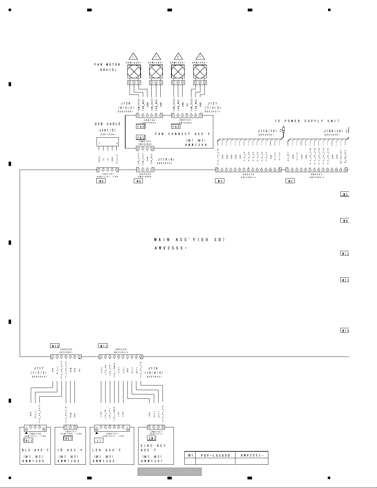
4.13 LED and IR ASSYS
A
2 3 4
B
C
D
E
F
38
1
2 3 4
PDP-LX5090
Page 39

5
*1: Notify upon the power-down content by Red LED flashing number of times.
*2: Notify upon the shutdown content by Blue LED flashing number of times
*3: Notify upon the subcategory number by Orange LED flashing number of times.
*4: PDP-LX5090H only
*5: Notify upon the abnormal state by Orange LED flashing number of times.
POWER ON STANDBY TIMER
Status
LED
LED Pattern/Remarks
Blue
Red
Orange
Blue
Red
Orange
Blue
Red
Orange
Blue
Red
Orange
Blue
Red
Orange
Blue
Red
Orange
Blue
Red
Orange
Blue
Red
Orange
Blue
Red
Orange
Blue
Red
Orange
Blue
Red
Orange
Blue
Red
Orange
Blue
Red
Orange
Blue
Red
Orange
Blue
Red
Orange
Blue
Red
Orange
LED Pattern
[1] LED DISPLAY INFORMATION
AC OFF or
Main Power Switch OFF
Standby Power
Management
Power On
Power-Down
Shutdown
Updating the PC
Sleep timer
Shutdown
(Subcategory flashing)
No digital adjustment
data copied for backup
During factory operation
During USB update
During DTB
communication inhibit
Updating of USB is
abnormally finished.
During reservation video
recording (Unit: Standby)
During reservation video
recording (Unit: ON)
Updating of USB is
finished normally.
Once Twice n times 2.5s Once
*1
500ms
500ms
*2
Once Twice n times 2.5s Once
500ms
*2
Once Twice n times 2.5s Once
*3
500ms
200ms
100ms
100ms
100ms
*4
100ms
*4
100ms
100ms
*4
100ms
100ms
*4
100ms
*5
500ms Once 500ms Twice 500ms n Times 2.5sec 500ms
*4
*4
5. DIAGNOSIS
5.1 POWER SUPPLY OPERATION
6 7 8
A
B
C
D
E
F
PDP-LX5090
5
6 7 8
39
Page 40

1
1 : The remote control (or KEY) signal is input to the IF microcomputer.
2 : The IF microcomputer sends the operation data of the remote control unit (or KEY) to the main microcomputer.
3 : The main microcomputer issues a startup command (PON) to the MOD microcomputer.
4 : The relay is controlled with logical OR interpretation of control signals by the main microcomputer and
module (MOD) microcomputer.
MOD
Microcomputer
IC3601
MAIN
Microcomputer
IC7003
IF
Microcomputer
IC6811
Power MOD
RELAY Control
OR
REM
Inv. Amp
Q8751
REM
infrared
receiver
Side Keys
SR OUT Jack
JA7871
4
1
2
1
RELAY2
SR_OUT
KEY_1
KEY_2
TXD_MD
RXD_MD
REQ_MD
SR_IN
TXD_IF
RXD_IF
CE_IF
REQ_IF
BUSY_IF
Inv. Amp
Q6812
Inv. Amp
Q4211
3
[2] POWER ON SEQUENCE
A
2 3 4
B
C
D
E
F
40
1
2 3 4
PDP-LX5090
Page 41

5
[3] DETAILS OF POWER ON SEQUENCE
AC
Microcomputer
output port setting
Microcomputer
input port state
All devices are not electrified.
Only the periphery of the IF microcomputer are electrified.
The user operation is invalid due to Main Switch off.
(*): PDP-LX5090H only
(*): PDP-LX5090H only
AC-OFF Main Power OFF, Passive Standby
AC-ON Main Power OFF, Passive Standby
OFF
OFF
OFF
OFF
OFF
OFF
OFF
IF: ACTIVE
OFF
Main: RELAY2
Main: PSW1
Module: DRF_B
Main: RST4
Main: RST2
Module: RST2
Microcomputer
output port setting
Microcomputer
input port state
OFF
OFF
OFF
OFF
OFF
OFF
OFF
IF: ACTIVE
OFF
Main: RELAY2
Main: PSW1
Module: DRF_B
Main: RST4
Main: RST2
Module: RST2
Main
Digital
Sensor
X/Y Drive, SCAN
Address
Main
Digital
Sensor
X/Y Drive, SCAN
Address
Power supply
Power supply
IO_AUDIO
IO_AUDIO
Main
Switch
AC
Main
Switch
IF ucom
Main_
ucom
Module_
ucom
OR
RELAY
DAC
ASIC
LED
DRIVE
SCAN
AND
ADDRESS
DRIVE
SCAN
TEMP1
BACK_EEP
PSW1
AND
RELAY2
RST2
RST4
ACTIVE
DRF_B
EMG_DDC
RST2
AD
M_SW_DET
ON OFF
FAN
ASIC
RST3
M_SW_DET_B
M_SW_DET
AC_DET
Vs/Va
Trans
Vcc
Trans
STB
Trans
AC_DET
V+3_4V_STB
V+5_1V_STB
V+17V
V+12V
V+6_5V
VSUS
VADR
OR
PS_PD
EXT_PD
A.TUNER
D.TUNER
(XDA)
PD
PD PD
SW
EEPROM
DCDC/REG
D-AMP
DCDC/REG
DCDC/REG
IR
KEY
232C
CEC
ucom
TEMP2
RGB-SW
VDEC
HDMI
ASIC
PS_PD/PD_TRG_B
EXT_PD
RELAY
VBI
REG
AV-SW
DCDC/REG
RLS
EEPROM
SW
V+6_5V
A.D.TUNER
COFDEM
BCM
A.D.TUNER
MPX
DEMOD
BCM
MAP
COLOR-S
A.D.TUNER
COFDEM
CIF
BCM(*)
MSP
SAT.
TUNER
S2DEMOD
CIMAX
LNB
CARD (*)
CARD (*)
IF ucom
Main_
ucom
Module_
ucom
OR
DAC
ASIC
LED
DRIVE
SCAN
AND
ADDRESS
DRIVE
SCAN
TEMP1
BACK_EEP
PSW1
AND
RELAY2
RST2
RST4
ACTIVE
DRF_B
EMG_DDC
RST2
AD
M_SW_DET
ON OFF
"kill me"
FAN
ASIC
RST3
M_SW_DET_B
M_SW_DET
AC_DET
Vs/Va
Trans
Vcc
Trans
STB
Trans
AC_DET
V+3_4V_STB
V+5_1V_STB
V+17V
V+12V
V+6_5V
VSUS
VADR
OR
PS_PD
EXT_PD
A.TUNER
D.TUNER
(XDA)
PD
PD PD
SW
EEPROM
DCDC/REG
DCDC/REG
DCDC/REG
IR
KEY
232C
CEC
ucom
TEMP2
RGB-SW
VDEC
HDMI
ASIC
PS_PD/PD_TRG_B
EXT_PD
RELAY
VBI
AV-SW
DCDC/REG
RLS
EEPROM
SW
V+6_5V
A.D.TUNER
COFDEM
BCM
A.D.TUNER
MPX
DEMOD
BCM
MAP
PC
COLOR-S
(Elite)
A.D.TUNER
COFDEM
CIF
BCM(*)
MSP
SAT.
TUNER
S2DEMOD
CIMAX
LNB
D-AMP
REG
RELAY
Front LED: OFF
Front LED: OFF
RELAY1
•KDD
Module: RELAY1•KDD
Module: RELAY1•KDD
RELAY1
•KDD
6 7 8
A
B
C
D
E
F
5
6 7 8
PDP-LX5090
41
Page 42

1
Microcomputer
output port setting
Microcomputer
input port state
OFF
ON
OFF
OFF
OFF
OFF
OFF
IF: ACTIVE
OFF
Main: RELAY2
Main: PSW1
Module: DRF_B
Main: RST4
Main: RST2
Module: RST2
Front LED: OFF
Microcomputer
output port setting
Microcomputer
input port state
OFF
OFF
OFF
OFF
OFF
OFF
OFF
IF: ACTIVE
OFF
Main: RELAY2
Main: PSW1
Module: DRF_B
Main: RST4
Main: RST2
Module: RST2
Front LED: RED
Periphery of the IF, Main and Module microcomputers are operated.
The user operation is invalid due to Main Switch off.
Only the periphery of the IF microcomputer is electrified.
The user operation is valid.
AC-ON Main Power OFF, Active Standby
AC-ON Main Power ON, Passive Standby
Main
Digital
Sensor
X/Y Drive, SCAN
Address
Main
Digital
Sensor
X/Y Drive, SCAN
Address
Power supply
Power supply
AC
Main
Switch
AC
Main
Switch
IF ucom
Main_
ucom
Module_
ucom
OR
RELAY
DAC
ASIC
LED
DRIVE
SCAN
AND
ADDRESS
DRIVE
SCAN
TEMP1
BACK_EEP
PSW1
AND
RELAY2
RST2
RST4
ACTIVE
DRF_B
EMG_DDC
RST2
AD
M_SW_DET
ON OFF
FAN
ASIC
RST3
M_SW_DET_B
M_SW_DET
AC_DET
Vs/Va
Trans
Vcc
Trans
STB
Trans
AC_DET
V+3_4V_STB
V+5_1V_STB
V+17V
V+12V
V+6_5V
VSUS
VADR
OR
PS_PD
EXT_PD
A.TUNER
D.TUNER
(XDA)
PD
PD PD
SW
EEPROM
DCDC/REG
D-AMP
DCDC/REG
DCDC/REG
IR
KEY
232C
CEC
ucom
TEMP2
RGB-SW
VDEC
HDMI
ASIC
PS_PD/PD_TRG_B
EXT_PD
RELAY
VBI
REG
AV-SW
DCDC/REG
RLS
EEPROM
SW
V+6_5V
A.D.TUNER
COFDEM
BCM
A.D.TUNER
MPX
DEMOD
BCM
MAP
PC
COLOR-S
(Elite)
A.D.TUNER
COFDEM
CIF
BCM(*)
MSP
SAT.
TUNER
S2DEMOD
CIMAX
LNB
IF ucom
Main_
ucom
Module_
ucom
OR
RELAY
DAC
ASIC
LED
DRIVE
SCAN
AND
ADDRESS
DRIVE
SCAN
TEMP1
BACK_EEP
PSW1
AND
RELAY2
RST2
RST4
ACTIVE
DRF_B
EMG_DDC
RST2
AD
M_SW_DET
ON OFF
"Kill me"
FAN
ASIC
RST3
M_SW_DET_B
M_SW_DET
AC_DET
Vs/Va
Trans
Vcc
Trans
STB
Trans
AC_DET
V+3_4V_STB
V+5_1V_STB
V+17V
V+12V
V+6_5V
VSUS
VADR
OR
PS_PD
EXT_PD
A.TUNER
D.TUNER
(XDA)
PD
PD PD
SW
EEPROM
DCDC/REG
D-AMP
DCDC/REG
DCDC/REG
IR
KEY
232C
CEC
ucom
TEMP2
RGB-SW
VDEC
HDMI
ASIC
PS_PD/PD_TRG_B
EXT_PD
RELAY
VBI
REG
AV-SW
DCDC/REG
RLS
EEPROM
SW
V+6_5V
A.D.TUNER
COFDEM
BCM
A.D.TUNER
MPX
DEMOD
BCM
MAP
PC
COLOR-S
(Elite)
A.D.TUNER
COFDEM
CIF
BCM(*)
MSP
SAT.
TUNER
S2DEMOD
CIMAX
LNB
(*): PDP-LX5090H only
IO_AUDIO
CARD (*)
(*): PDP-LX5090H only
IO_AUDIO
CARD (*)
RELAY1
•KDD
Module: RELAY1•KDD
RELAY1
•KDD
Module: RELAY1•KDD
A
2 3 4
B
C
D
E
F
42
1
2 3 4
PDP-LX5090
Page 43

5
Microcomputer
output port setting
Microcomputer
input port state
OFF
ON
ON
OFF
OFF
OFF
IF: ACTIVE
ON
Main: RELAY2
Main: PSW1
Module: DRF_B
Main: RST4
Main: RST2
Module: RST2
OFF
Front LED: RED
Microcomputer
output port setting
Microcomputer
input port state
OFF
ON
OFF
OFF
OFF
OFF
OFF
IF: ACTIVE
OFF
Main: RELAY2
Main: PSW1
Module: DRF_B
Main: RST4
Main: RST2
Module: RST2
Front LED: RED
Periphery of the IF, Main and Module microcomputers are operated.
The user operation is valid.
AC-ON Main Power ON, Active Standby
AC-ON Main Power ON, Function Standby
Main
Digital
Sensor
X/Y Drive, SCAN
Address
Main
Digital
Sensor
X/Y Drive, SCAN
Address
Power supply
Power supply
AC
Main
Switch
AC
Main
Switch
Standby power device and some Vcc power devices operate.
The user operation is valid.
RGB-SW/AD/D-AMP/MAP are electrified, but uses the power-saving mode function of the IC.
IF ucom
Main_
ucom
Module_
ucom
OR
RELAY
DAC
ASIC
LED
DRIVE
SCAN
AND
ADDRESS
DRIVE
SCAN
TEMP1
BACK_EEP
PSW1
AND
RELAY2
RST2
RST4
ACTIVE
DRF_B
EMG_DDC
RST2
AD
M_SW_DET
ON OFF
"POF"
FAN
ASIC
RST3
M_SW_DET_B
M_SW_DET
AC_DET
Vs/Va
Trans
Vcc
Trans
STB
Trans
AC_DET
V+3_4V_STB
V+5_1V_STB
V+17V
V+12V
V+6_5V
VSUS
VADR
OR
PS_PD
EXT_PD
A.TUNER
D.TUNER
(XDA)
PD
PD PD
SW
EEPROM
DCDC/REG
D-AMP
DCDC/REG
DCDC/REG
IR
KEY
232C
CEC
ucom
TEMP2
RGB-SW
VDEC
HDMI
ASIC
PS_PD/PD_TRG_B
EXT_PD
RELAY
VBI
REG
AV-SW
DCDC/REG
RLS
EEPROM
SW
V+6_5V
A.D.TUNER
COFDEM
BCM
A.D.TUNER
MPX
DEMOD
BCM
MAP
PC
COLOR-S
(Elite)
A.D.TUNER
COFDEM
CIF
BCM(*)
MSP
SAT.
TUNER
S2DEMOD
CIMAX
LNB
(*): PDP-LX5090H only
IO_AUDIO
CARD (*)
(*): PDP-LX5090H only
IO_AUDIO
CARD (*)
RELAY1
•KDD
Module: RELAY1•KDD
RELAY1
•KDD
Module: RELAY1•KDD
6 7 8
A
B
C
5
PDP-LX5090
6 7 8
D
E
F
43
Page 44

1
AC
All devices are operated.
AC-ON Main Power ON, PDP Screen ON
Main
Digital
Sensor
X/Y Drive, SCAN
Address
Power supply
Main
Switch
IF ucom
Main_
ucom
Module_
ucom
OR
RELAY
DAC
ASIC
LED
DRIVE
SCAN
AND
ADDRESS
DRIVE
SCAN
TEMP1
BACK_EEP
PSW1
AND
RELAY2
RST2
RST4
ACTIVE
DRF_B
EMG_DDC
RST2
AD
M_SW_DET
ON OFF
"PON"
FAN
ASIC
RST3
M_SW_DET_B
M_SW_DET
AC_DET
Vs/Va
Trans
Vcc
Trans
STB
Trans
AC_DET
V+3_4V_STB
V+5_1V_STB
V+17V
V+12V
V+6_5V
VSUS
VADR
OR
PS_PD
EXT_PD
A.TUNER
D.TUNER
(XDA)
PD
PD PD
SW
EEPROM
DCDC/REG
D-AMP
DCDC/REG
DCDC/REG
IR
KEY
232C
CEC
ucom
TEMP2
RGB-SW
VDEC
HDMI
ASIC
PS_PD/PD_TRG_B
EXT_PD
RELAY
VBI
REG
AV-SW
DCDC/REG
RLS
EEPROM
SW
V+6_5V
A.D.TUNER
COFDEM
BCM
A.D.TUNER
MPX
DEMOD
BCM
MAP
PC
COLOR-S
(Elite)
A.D.TUNER
COFDEM
CIF
BCM(*)
MSP
SAT.
TUNER
S2DEMOD
CIMAX
LNB
(*): PDP-LX5090H only
IO_AUDIO
CARD (*)
Microcomputer
output port setting
Microcomputer
input port state
ON
ON
ON
ON
ON
ON
ON
IF: ACTIVE
ON
Main: RELAY2
Main: PSW1
Module: DRF_B
Main: RST4
Main: RST2
Module: RST2
Front LED: BLUE
RELAY1
•KDD
Module: RELAY1•KDD
A
2 3 4
B
C
D
E
F
44
PDP-LX5090
1
2 3 4
Page 45

5
Flowchart of Failure Analysis for The Whole Unit
START
Is the STB LED lit?
Is STB 3.4 V power supplied?
(Check the power at the IF microcomputer on the MAIN Assy.)
Can the unit be turned on
(Relay ON)?
Is the panel arbitrary turned on or
off repeatedly? Or do luminescent
spots appear on the screen?
A shutdown occurs.
Are the voltages at AC_DET and
MSW_DET on the POWER
SUPPLY Unit high?
Replace the POWER SUPPLY
Unit.
Check if the cable that connects
the POWER SUPPLY and MAIN
Assys is firmly connected.
In the power startup, the Main microcomputer
controls a relay port earlier than module
microcomputer.
• Check the DRF SW.
• Before turning the drive off with the RS-232C
commands or using the remote control unit,
turn the unit off.
In a case where luminescent spots appear
or the panel is repeatedly turned on or off.
In a case where luminescent spots appear.
(*1): As reset lighting of the 9th-generation panel is faint,
reduce the ambient lighting when checking the display.
Is the voltage at the RELAY port
of the connectors between the
DIGITAL Assy and POWER
SUPPLY Unit H (3.4 V)?
No
No
Is the drive off?
Turn the drive on.
No
Ye s
Ye s
Ye s
A shutdown occurs.
See "5.4 DIAGNOSIS OF SD (SHUTDOWN)."
For PDP-LX5090H, refer to the sction "3.3 DIAGNOSIS OF SD (SHUTDOWN)"
of the Service Manual for PDP-LX5090H.
See "5.4 DIAGNOSIS OF SD (SHUTDOWN)."
For PDP-LX5090H, refer to the sction "3.3 DIAGNOSIS OF SD (SHUTDOWN)"
of the Service Manual for PDP-LX5090H.
Ye s
A power-down occurs.
Does the screen display reset
lighting? (*1)
See "5.3 DIAGNOSIS OF PD (POWER-DOWN)."
Ye s
When the panel drive-power is in OFF state, there will be no PD,
except PS_PD.
When the panel drive-power is in OFF state, there will be no PD,
except PS_PD.
A power-down occurs.
See "5.3 DIAGNOSIS OF PD (POWER-DOWN)."
Ye s
No
No
Ye s
No
NG
No
Ye s
Ye s
Ye s
Ye s
No
No
Ye s
No
No
No
Ye s
Problems concerning STB status
Note: Check that the Main power SW is ON side.
Problems concerning the power
Problems concerning lighting of the panel
Failure analysis for the
MAIN Assy => MA1
Failure analysis for the
MAIN Assy => MA2
Failure analysis for the
POWER SUPPLY Unit => PS1
Failure analysis for the
POWER SUPPLY Unit => PS2
Failure analysis for the
POWER SUPPLY Unit => PS3
Failure analysis for the
drive system => DR1
Failure analysis for the
drive system => DR2
A
The green/red LEDs on the DIGITAL Assy indicate ON/STB
of the panel and causes for a power-down or shutdown.
If neither the green nor red LED lights, it is likely that the
power to the STB system is not supplied. (failure, PASV-STB status)
If AC_DET or MSW_DET is Low, LED goes off.
[1] WHOLE UNIT
5.2 DIAGNOSIS FLOWCHART OF FAILURE ANALYSIS
6 7 8
A
B
C
D
5
PDP-LX5090
6 7 8
E
F
45
Page 46

1
• Check with the combination of the animated/slanting ramp or other mask patterns and mirror function.
* Animated pattern: For checking erroneously discharged cells, load change is constantly caused on a screen.
* Ramp pattern: For checking gradation expression
* Mirror function: For checking if a defective indication is interlocked with mirror inversion, in order to identify a defective point
Is the on-screen display (OSD)
properly displayed?
Is the audio signal output?
Is the panel mask properly
displayed?
No
No
Ye s
Check on the Factory menu.
Is an external video signal
displayed properly?
Specific failure whose cause is
difficult to identify in the initial stage
No
No
Failure analysis for the
audio system => AU1
Ye s
Ye s
Ye s
In the subsequent diagnostic steps, it is most likely that the multi base section is in failure.
Problems concerning video display
Problems concerning the audio output
A
Failure analysis for the
DIGITAL Assy => DG1
Failure analysis for the MAIN Assy => MA3
For PDP-LX5090H, refer to the "Failure analysis for the MAIN Assy => MA3” on the sction
"3.1 [5] MAIN ASSY" of the Service Manual for PDP-LX5090H.
Failure analysis for the
drive system => DR2
Is the abnormality associated
with one scan IC block?
Ye s
Is there any local abnormality
on the screen?
Is the abnormality associated
with one ADDRESS or one TCP?
No
No
Ye s
Failure analysis for the
drive system => DR3
Failure analysis for the
drive system => DR4
Ye s
No
Replace the panel chassis.
A
2 3 4
B
C
D
E
F
46
PDP-LX5090
1
2 3 4
Page 47

5
[2] POWER SUPPLY UNIT
Flowchart of Failure Analysis for The POWER SUPPLY Unit
Is the cable connected firmly to
the P7 connector?
Is the cable to the P7 connector
broken?
Check the voltage at the MAIN Assy and
POWER SUPPLY Unit.
Check the resistance between D112 cathode
and JW194 (jumper),
using a tester.
Properly connect the cable between
the P7 and M2 connectors.
No
Replace the defective cable (J109).
Ye s
Ye s
Is the fuse (F102) blown?
Replace the POWER SUPPLY
Unit.
Replace the POWER SUPPLY
Unit.
Replace the POWER SUPPLY
Unit.
Replace the POWER SUPPLY
Unit.
Ye s
No
Is one of the limiting resistors
(R126) blown?
Ye s
No
The POWER SUPPLY Unit is
normal.
The POWER SUPPLY Unit is
normal.
STB 3.4 V power is not output.
No
Is the VADR voltage within the
specified values?
Is the VSUS voltage within the
specified range?
Is there a fluctuation in the
VADR voltage?
Is there a fluctuation in the
VSUS voltage?
The ripple must be within 5 V.
The ripple must be within 10 V.
The specified voltage values are between
72 and 78 V.
The specified voltage values are between
200 and 210 V (VSU: 125/35°C).
No
Ye s
Ye s
No
No
Ye s
Ye s
The cells of the panel do not
light normally.
No
The POWER SUPPLY Unit is
normal.
The power is not on, even though
the RELAY port is active.
Is the relay (RY102) on?
• Check the relay operation at the JW281
(jumper). (Voltage: 5 V)
• Check the relay sound (click).
No
Ye s
Is the PFC voltage normal?
• Check the voltage between the JW154
(jumper) (-) and JW139 (jumper) (+).
• The voltage must be around 400 V.
(340V or less are defective.)
Caution: High voltage!
Replace the POWER SUPPLY
Unit.
Replace the POWER SUPPLY
Unit.
Replace the POWER SUPPLY
Unit.
Replace the POWER SUPPLY
Unit.
No
Ye s
Failure analysis for the
POWER SUPPLY Unit => PS1
Failure analysis for the
POWER SUPPLY Unit => PS2
Failure analysis for the
POWER SUPPLY Unit => PS3
6 7 8
A
B
C
D
5
PDP-LX5090
6 7 8
E
F
47
Page 48

1
[3] DRIVE ASSY
Flowchart of Failure Analysis for The Drive Assy
X/Y DRIVE Assys
No
No
No
NG
NGYe s
Ye s
Ye s
Are the FFC cables properly
connected?
Are the panel FPC and SCAN Assys
connectors properly connected to
the X/Y DRIVE Assys?
Is the input signal normal?
Replace the panel chassis.
Ye s
Replace the X/Y DRIVE Assys.
NG
Replace the DIGITAL Assy.
Properly connect the panel FPC
and SCAN Assys connectors.
Properly connect the FFC cables.
No
Replace the FFC cables.
Reset lighting is not displayed.
Is the waveform normal when the
voltage is applied to the panel?
Failure analysis for the
drive system => DR1
A
2 3 4
B
C
D
E
F
48
1
2 3 4
PDP-LX5090
Page 49

No
Y DRIVE Assy
Is the waveform normal when the
voltage is applied to the panel?
(See the oscilloscope photos.)
Are all the connectors properly
connected?
Reconnect the connectors.
No
To " 8.4. Adjustment when the Service
Panel Assy is Replaced"
No
Set the VH voltage correctly.
X DRIVE Assy
Y DRIVE Assy / SCAN Assy
ADDRESS Assy
Is the adjustment value of each
voltage within the appropriate range?
Abnormality across the whole
screen such as luminescent spots.
B
D
C
Ye s
Ye s
No
Is the VH set voltage (140 V)
correctly set?
Ye s
Is the output value of each voltage
from the Y DRIVE Assy appropriate?
Another Assy may
be in failure.
No
Replace the FFC cables.
Replace the DIGITAL Assy.
Replace the Y DRIVE Assy.
Replace the SCAN IC.
NG
Ye s
Ye s
Ye s
No
Is the input signal normal?
(See the oscilloscope photos.)
No
Is the waveform of the control
signal from the SCAN Assy normal?
(See the oscilloscope photos.)
Failure analysis for the
drive system => DR2
Because it is difficult to identify which drive is in failure, follow the flowchart below to check each Assy.
* Using ADJ1 on the Panel Factory menu or the QAJ
command, check if the adjustment value is within the
range described in the table below
When go forward to the section "8.4 Adjustment when the service panel Assy
is replaced" from this step, please be careful to the following items.
• Do not clear hour meter and pulse meter.
(for readjustment in the panel non-replacement)
• Input a setting value of label mention example as preparations
(because a product panel does not have a label)
• Compare the measurement value at the last output stage of each
voltage against the value calculated using the measurement value
of the DAC output voltage. (See the table below.)
• There may be a case where the setting of an adjustable resistor on
the Assy is out of range.
5
6 7 8
A
B
C
D
5
PDP-LX5090
6 7 8
E
F
49
Page 50

1
Is the waveform normal when the
voltage is applied to the panel?
(See the oscilloscope photos.)
No
Is the output value of each voltage
from the X DRIVE Assy appropriate?
Another Assy may
be in failure.
Ye s
Replace the X DRIVE Assy.
Replace the DIGITAL Assy.
NG
No
Ye s
No
Is the input signal normal?
(See the oscilloscope photos.)
Replace the FFC cables.
* Waveform such as the
signal is OK for an
LVDS signal.
No
Are all the connectors properly
connected?
Reconnect the connectors.
B
D
Ye s
X DRIVE Assy
No
Are all the connectors properly
connected?
Reconnect the connectors.
No
C
No
Ye s
Is the TCP control signal normal?
(See the oscilloscope photos.)
Ye s
ADDRESS Assy
Replace the panel chassis.
Replace the DIGITAL Assy.
Ye s No
NG
Replace the FFC cables.
Is the input signal normal?
(See the oscilloscope photos.)
• Compare the measurement value at the last output stage of each
voltage against the value calculated using the measurement value
of the DAC output voltage. (See the table below.)
• There may be a case where the setting of an adjustable resistor on
the Assy is out of range.
A
2 3 4
B
C
D
E
F
50
PDP-LX5090
1
2 3 4
Page 51

5
(*1): These parts have not been mounted.
(*2): It is recommended to measure the DAC output voltage with the drive off.
(*3): View when the Assy is mounted on the unit and viewed from the rear.
(*4): The value calculated using an adjustment value may be different from the
value measured at the last output stage, because various corrections such
as temperature correction are not taken into consideration.
VSNOFS
VYRST
VKNOFS1_2
VKNOFS3
VKNOFS4
XKOFS1
XKOFS2
040 to 085
001 to 056
054 to 107
065 to 117
111 to 164
105
063
101 to 157
001 to 074
121 to 164
107 to 149
151 to 193
085
047
A
B
C
D
E
F
G
H
I
J
R2754,R2755,R2757
R2723
R2621
CN2405
CN2403,CN2406
CN2404
CN2401
K1401
K1402
CN1301,CN1302
CN2404 (*1)
CN2401 (*1)
CN2405 (*1)
CN2403 (*1)
CN2406 (*1)
CN1302 (*1)
CN1301 (*1)
Lower side of R2723 (*3)
Upper side of R2621 (*3)
Left side of R2754 (*3)
Right side of R2757 (*3)
Right side of R2755 (*3)
K1402 (*1)
K1401 (*1)
VOFS_ADJ × 13.91 + 55.54
VYPRST_ADJ × 62.495 + 75.2
YVKNOFS1_ADJ × 36.85 + 159.3
YVKNOFS3_ADJ × 36.85 + 159.3
YVKNOFS4_ADJ × 36.85 + 159.3
XKNOFS1_ADJ × 27.3 + 30
XKNOFS2_ADJ × 25.0 + 69.8
VOF value × 0.18 + 9.6
VRP value × 0.81 + 74.4
(V1F value+VYF value-128)
× 0.48 + 158.8
(V3F value+VYF value-128)
× 0.48 + 158.8
(V4F value+VYF value-128)
× 0.48 + 158.8
VX1 value × 0.35 + 29.7
VX2 value × 0.32 + 69.5
Y DRIVE
Assy
X DRIVE
Assy
Adjustable Range
Assy Name
Voltage to be
Checked (V)
60-inch 50-inch
Output at the
Last Stage
DAC Output (*2)
Computation Using
DAC Output Voltage (V)
Computation Using Adjustment
Value (*4)
Measurement Point
Computation Formula for Voltage (Absolute Value)
EDAF
Diagrammatic view of the Y DRIVE Assy Diagrammatic view of the X DRIVE Assy
G
C
B
H
J
I
6 7 8
A
B
C
D
E
F
PDP-LX5090
5
6 7 8
51
Page 52

1
Is the TCP control signal normal?
No
NG
NG
Ye s Ye s
No
Are the FFC cables properly
connected?
Replace the DIGITAL Assy.
Properly connect the FFC cables.
The abnormality is associated with
one ADDRESS or one TCP.
Diagnose the ADDRESS Assy.
In most cases of damage on one line,
the panel chassis must be replaced.
If the FFC cable that connects the DIGITAL and ADDRESS Assys is in failure,
the abnormality is associated with one address in most cases.
Replace the panel chassis.
No
NG
Ye s
Ye s
Ye s
No
Is the 15P connector connected
properly to the socket?
Reconnect the connector properly.
NG
Is the waveform of the SCAN IC
control signal from the Y DRIVE
Assy normal?
No
Replace the Y DRIVE Assy.
The abnormality is associated
with a single scan line.
Diagnose the SCAN Assy.
Replace the SCAN IC.
Replace the panel chassis.
Failure analysis for the
drive system => DR3
Failure analysis for the
drive system => DR4
Is the waveform normal when the
voltage is applied to the panel?
(See the oscilloscope photos.)
Note1
Note 1:
In a case where confirmation of the waveform for a particular line is impossible with
an oscilloscope, it is possible to identify a defective line by lighting a particular line,
using the following commands: (The SCAN IC outputting each line refers to the table.)
PON
FAY
MKRS01
BSMS01 (Command for reducing phosphor burn-in)
$250000∗∗∗∗ (In place of ∗∗∗∗, input a figure between 0001 and 1080, which denotes
an ordinal number of a particular line.)
With the above commands, a particular line lights. Be careful to light a line for as
short a time as possible, to avoid phosphor burn-in.
After a particular line is identified, display an all-white screen to protect the screen
from burn-in.
IC No.
No 1
No 2
No 3
No 4
No 5
No 6
No 7
No 8
No 9
No 10
No 11
No 12
No 13
No 14
No 15
No 16
Line Number
66
68
68
68
68
68
68
66
66
68
68
68
68
68
68
66
Object Line
0001 to 0066
0067 to 0134
0135 to 0202
0203 to 0270
0271 to 0338
0339 to 0406
0407 to 0474
0475 to 0540
0541 to 0606
0607 to 0674
0675 to 0742
0743 to 0810
0811 to 0878
0879 to 0946
0947 to 1014
1015 to 1080
A
2 3 4
B
C
D
E
F
52
1
2 3 4
PDP-LX5090
Page 53

5
[4] DIGITAL ASSY
Flowchart of Failure Analysis for The DIGITAL Assy
Is an appropriate signal input?
(Check the V frequency with the
QSI command.)
Is the sync signal properly output
from the MAIN Assy?
Disconnect and reconnect the
50P (J212) FFC/40P (J211) FFC.
• If the OSD is not properly displayed although the panel mask is properly displayed,
a failure exists in the path from the output of IC2801 on the MAIN Assy to IC3301 on the DIGITAL Assy.
-> If only the OSD is abnormal, the MAIN Assy is in failure.
• If no vertical sync signal is input to the DIGITAL Assy,
a freeze-frame picture will be displayed.
• It is most likely that the video signal
and sync signal data are abnormal.
No
No
No
NG
Failure in connectors CN3201 or
CN3202 on the DIGITAL Assy.
Failure in ASIC (IC3301) on the
DIGITAL Assy.
Replace the MAIN Assy.
Replace the 50P (J212) FFC/
40P (J211) FFC.
NG
Ye s
OKNG
Replace the DIGITAL Assy.
The on-screen display (OSD) is
not properly indicated.
Failure analysis for the
DIGITAL Assy => DG1
6 7 8
A
B
C
D
E
F
PDP-LX5090
5
6 7 8
53
Page 54

1
[5] MAIN ASSY
Flowchart of Failure Analysis for The MAIN Assy
Failure in the RST IC (IC8302) output or its peripheral circuits
No
Replace the MAIN Assy.
No
Turn the POWER switch on.
The STB LED does not light although
STB 3.4 V power is supplied.
Does the POWER switch on?
No
Is the M11 connector securely
connected?
Securely connect the M11 connector.
Ye s
Ye s
Is the cable that is connected to
the M11 connector broken?
Replace the cable (J116).
No
No
No
NG
NG
The RELAY port does not work.
The power is not turned on.
Is voltage at REQ_IF on the MAIN
Assy High (3.3 V)?
Can the unit be turned on, using
the remote control unit?
Can the unit be turned on, using
the Power switch on the unit?
Can the unit be turned on, using
RS-232C commands?
Ye s
Ye s
Is resetting of the IF
microcomputer canceled?
Failure in the line between the IF microcomputer and M11 connector
No
Replace the MAIN Assy.
Ye s
Is the voltage at Pin 3 of the M11
connector High?
Relay control is unable unless it supplies a power supply to the module microcompute.
No
Replace the MAIN Assy.
Ye s
Is the voltage at Pin 50 of the M4
connector 3.4 V?
No
Replace the MAIN Assy.
Ye s
Are the voltages (1.5 V/2.5 V/3.4 V)
supplied to the main microcomputer?
No problem with the MAIN Assy.
Check the LED Assy.
No
Ye s
Ye s
Ye s
Replace the cable (J117) that
connects between the IR and
MAIN Assys.
Replace the cable (J116) that
connects between the SIDE KEY
and MAIN Assys.
Replace the IR Assy.
Replace the SIDE KEY Assy.
Replace the MAIN Assy.
Replace the MAIN Assy.
Replace the MAIN Assy.
NG
No
NG
Replace the 50P cable (J213) that
connects between the IO and
MAIN Assys.
Replace the IO Assy.
Replace the MAIN Assy.
NG
NG
Failure analysis for the
MAIN Assy => MA1
Failure analysis for the
MAIN Assy => MA2
A
2 3 4
B
C
D
E
F
54
1
PDP-LX5090
2 3 4
Page 55

5
Flowchart of Failure Analysis for The Video System
Is the selected input signal a
terrestrial analog TV?
Are the data displayed on the
"HDMI SIGNAL INFO" page of
the Factory menu correct?
The source equipment previously
used is in failure.
No problem with the MAIN Assy.
Is the sync signal output from
IC4901?
Does the result of SIG mode
detection on the Factory menu
coincide with the input signal data?
Ye s
No
No
No
OK
After changing the source
equipment, check the "HDMI
SIGNAL INFO" data again.
NG
Replace the MAIN Assy.
No
Replace the MAIN Assy.
The input signal is not displayed.
=> ATV
Is the selected input signal a
composite signal?
Ye s
No
=> COMP / S1
=> COMP / PC2
Is the selected input signal a
component signal?
Ye s
=> COMP / PC1
Is the selected input signal a
S-video signal?
Is the selected input signal an
PC signal?
Ye s
No
Is the selected input signal an
HDMI signal?
Ye s
Ye s
=> DTV
Is the selected input signal a
digital TV signal?
Ye s
No problem with the MAIN Assy
No
No
Ye s
Ye s
Ye s
Is the sync signal input to IC6501?
No
Replace the MAIN Assy.
Replace the MAIN Assy.
Ye s
Replace the MAIN Assy.
No
No
=> COMP / S1
Is the selected input signal a
RGB signal (SCART)?
Ye s
No
=> RGB
Failure analysis for the
MAIN Assy => MA3
6 7 8
A
B
C
D
5
PDP-LX5090
6 7 8
E
F
55
Page 56

1
[6] VIDEO SYSTEM
Flowchart of Failure Analysis for The Video System
Is the input selecter set to TV?
(Analog)
Set the Input selector to TV.
(Analog)
No
No
Check the 40P FFC (J214) between MAIN Assy and IO
Assy. If there was problem, replace it.
No
Check around IC8001 and check the communications
between IC8001 and microcomuputer.
If there was no ploblem, replace the IO Assy.
Check around IC4702 and check the communications
between IC4702 and microcomuputer.
If there was no ploblem, replace the MAIN Assy.
No
Check around the IC that is found to have failure in
communication and the microcomputer.
If there was no ploblem, replace the MAIN Assy.
No
No
No
Replace the MAIN Assy.
Ye s
Ye s
Analog tuner signal is not
displayed on the screen.
=> ATV
Is a signal input to IC8001
(AVSW)? (pin 60)
Has the signal arrived at emitter
of Q5304?
No
Replace the U5301 (TUNER).
Is a signal input to TP7563?
No
Check the 40P FFC (J214) between the MAIN Assy and IO Assy.
If there was problem, replace it.
Ye s
Which signal is not output,
main or sub signal?
Is a signal output from IC8001?
(AVSW) (pin 45)
Are the data output from IC4702?
(VDEC) (pins 93 to 97, 99 to 104,
107 to 109)
Ye s
Has the signal arrived at IC4702?
(VDEC) (pin 22)
Ye s
Ye s
Ye s
Is the communication between
each IC (VDEC, ASIC) on the
MAIN Assy and the microcomputer
normal?
Ye s
Has the signal arrived at IC4702?
(pin 70)
Ye s
MAIN
SUB
1
No
Is a HS signal input to IC6811
(IFUCOM)? (pin 3)
Has the signal arrived at pin 6 of
Q5307?
Has the signal arrived at R5303.
No No
Replace the U5301 (TUNER).
Ye s
2
4
5
4
No
No
Are the data output from IC4702?
(pins 79 to 86, 88 to 90)
Ye s
5
Is a signal output from IC4601?
(pin 49)
3
3
2
IC6811 - pin 3
V: 1 V/div H: 10 μsec/div
1
IC8001 - pin 60 (in)
V: 500 mV/div H: 10 μsec/div
3
IC8001 - pins 45, 49 (out)
V: 500 mV/div H: 10 μsec/div
4
IC4702 - pins 22, 70
V: 500 mV/div H: 10 μsec/div
5
IC4702 (out)
V: 1 V/div H: 2 μsec/div
Waveforms
Input signal: PAL Color-bar (Analog tuner)
A
2 3 4
B
C
D
E
F
56
1
2 3 4
PDP-LX5090
Page 57

Is the function correspondeing to
selected signal input selected?
Select the corresponding signal
with the Input selector.
No
Check the 40P FFC (J214) between MAIN Assy and
IO Assy. If there was problem, replace it.
No
Check around IC8001 and check the communications
between IC8001 and microcomuputer.
If there was no ploblem, replace the IO Assy.
No No
No
Check around the input terminals.
No
Replace the IO Assy.
NG
Ye s
Ye s
Image for the composite or S-video
signal is not displayed.
=> COMP/S1
Has the signal arrived at IC8001?
(AVSW)
Which signal is not output,
main or sub signal?
Is a signal output from IC8001?
(AVSW) (pins 42, 45)
Ye s
Has the signal arrived at IC4702?
(VDEC) (pins 22, 26)
Ye s
Has the signal arrived at IC4702?
(pins 69, 70)
Ye s
Ye s
Ye s
MAIN
SUB
76
9
11
Is a signal output from IC8001?
(pins 47, 49)
1312
1514
8
10
6
IC8001 - pins 87, 93 (Y)
V: 500 mV/div H: 20 μsec/div
7
IC8001 - pins 89, 95 (C)
V: 500 mV/div H: 20 μsec/div
8
IC8001 - pin 45 (Main Y)
V: 500 mV/div H: 20 μsec/div
9 10
IC8001 - pin 42 (Main C)
V: 500 mV/div H: 20 μsec/div
IC4702 - pin 22 (Main Y)
V: 500 mV/div H: 20 μsec/div
11
IC4702 - pin 26 (Main C)
V: 500 mV/div H: 20 μsec/div
12
IC8001 - pin 49 (Sub Y)
V: 500 mV/div H: 20 μsec/div
13 14
IC8001 - pin 47 (Sub C)
V: 500 mV/div H: 20 μsec/div
IC4702 - pin 70 (Sub Y)
V: 500 mV/div H: 20 μsec/div
15
IC4702 - pin 69 (Sub C)
V: 500 mV/div H: 20 μsec/div
Waveforms
Input signal: PAL Color-bar (S termial)
Check around the IC that is found to have failure in
communication and the microcomputer.
If there was no ploblem, replace the MAIN Assy.
No
Replace the MAIN Assy.
Ye s
Ye s
Is the communication between
each IC (VDEC, ASIC) on the
MAIN Assy and the microcomputer
normal?
No
Specifications that does not
display in the sub-side.
Is the screen of main side Tuner?
5
6 7 8
A
B
C
D
5
6 7 8
PDP-LX5090
E
F
57
Page 58

1
No
No
Ye s
Ye s
Is the function correspondeing to
selected signal input selected?
Image for the RGB (SCART) input
signal is not displasyed.
Select the corresponding signal
with the Input selector.
Is the screen of main side Tuner?
No
Specifications that does not
display in the sub-side.
=> RGB
Sub
Main
Which signal is not output,
main or sub signal?
Check the 40P FFC (J214) between MAIN Assy and
IO Assy. If there was problem, replace it.
No
Check around the IC that is found to
have failure in communication and
the microcomputer. If there was no
ploblem, replace the MAIN Assy.
No
Check around IC8101 and check the
communications between IC8101
and microcomuputer. If there was
no ploblem, replace the IO Assy.
No
Replace the MAIN Assy.
Is a signal output from IC8101?
(pins 41, 43 and 45)
Has the signal arrived at IC4702?
(pins 27, 28 and 65)
Ye s
Ye s
Ye s
Is the communication between
each IC (VDEC, ASIC) on the
MAIN Assy and the microcomputer
normal?
Ye s
Has the signal arrived at IC8101
(RGBSW)?
212019
1716 18
16
IC8101 - pin 45 (G out)
V: 500 mV/div H: 20 μS/div
17 18
IC8101 - pin 41 (B out)
V: 500 mV/div H: 20 μS/div
19
IC4702 - pin 65 (GY)
V: 500 mV/div H: 20 μS/div
20
IC47021 - pin 27 (BCB)
V: 500 mV/div H: 20 μS/div
21
IC4702 - pin 28 (BCR)
V: 500 mV/div H: 20 μS/div
Waveforms
Input signal: PAL Color-bar (SCART RGB terminal)
IC8101 - pin 43 (B out)
V: 500 mV/div H: 20 μS/div
Check around the input terminals.
No
Replace the IO Assy.
A
B
2 3 4
C
D
E
F
58
PDP-LX5090
1
2 3 4
Page 59

Is the function corresponding to
selected signal input selected?
Select the corresponding signal
with the input selector.
No
No
NG
No
No
Ye s
Ye s
Image for the component signal
is not displayed.
=> COMP/PC1
Ye s
Is a signal output from IC8101?
(RGBSW) (pins 30, 32, 34)
Has the signal arrived at IC4801?
(ADC) (pins 43, 48, 54)
Ye s
Ye s
27
30
2625
2928
Check around the input terminals.
Replace the IO Assy.
No
Specifications that does not
display in the sub-side.
Has the signal arrived at IC8101?
(RGBSW) (pins 86, 88, 90)
SUB
Is the screen of main side Tuner?
Which signal is not output,
main or sub signal?
Ye s
MAIN
242322
Check around IC8101 and check the communications
between IC8101 and microcomuputer.
If there was no ploblem, replace the IO Assy.
Check the 40P FFC (J214) between MAIN Assy and
IO Assy. If there was problem, replace it.
Check around the IC that is found to have failure in
communication and the microcomputer.
If there was no ploblem, replace the MAIN Assy.
No
Replace the MAIN Assy.
Ye s
Is the communication between
each IC (ADC, ASIC) on the
MAIN Assy and the microcomputer
normal?
22
IC8101 - pin 86 (Y)
V: 500 mV/div H: 20 μsec/div
23
IC8101 - pin 88 (Pb)
V: 500 mV/div H: 20 μsec/div
24
IC8101 - pin 90 (Pr)
V: 500 mV/div H: 20 μsec/div
25 26
IC8101 - pin 34 (Y)
V: 500 mV/div H: 20 μsec/div
IC8101 - pin 32 (Pb)
V: 500 mV/div H: 20 μsec/div
27
IC8101 - pin 30 (Pr)
V: 500 mV/div H: 20 μsec/div
28
IC4801 - pin 48 (Y)
V: 500 mV/div H: 20 μsec/div
29 30
IC4801 - pin 43 (Pb)
V: 500 mV/div H: 20 μsec/div
IC4801 - pin 54 (Pr)
V: 500 mV/div H: 20 μsec/div
Waveforms
Input signal: Color-bar (Component 720p/50 Hz)
5
6 7 8
A
B
C
D
E
5
6 7 8
PDP-LX5090
F
59
Page 60

1
Is the function corresponding to
selected signal input selected?
Select the corresponding signal
with the input selector.
No
No
No
No
Ye s
Ye s
Image for the PC signals is not
displayed.
=> COMP/PC2
Ye s
Is a signal output from IC8101?
(RGBSW) (pins 30, 32, 34)
Has the signal arrived at IC4801?
(ADC) (pins 43, 48, 54)
Ye s
Ye s
38
41
3736
4039
No
Specifications that does not
display in the sub-side.
Has the signal arrived at IC8101?
(RGBSW) (pins 2, 4, 6, 14, 15)
SUB
Is the screen of main side Tuner?
Which signal is not output,
main or sub signal?
Ye s
MAIN
3332 353431
Check around IC8101 and check the communications
between IC8101 and microcomuputer.
If there was no ploblem, replace the IO Assy.
Check the 40P FFC (J214) between MAIN Assy and
IO Assy. If there was problem, replace it.
Check the 12P FFC (J215) between IO Assy and
PC Assy. If there was problem, replace it.
Check around the IC that is found to have failure in
communication and the microcomputer.
If there was no ploblem, replace the MAIN Assy.
No
Replace the MAIN Assy.
Ye s
Is the communication between
each IC (ADC, ASIC) on the
MAIN Assy and the microcomputer
normal?
31
IC8101 - pin 2 (G in)
V: 500 mV/div H: 10 μsec/div
32
IC8101 - pin 4 (B in)
V: 500 mV/div H: 10 μsec/div
33
IC8101 - pin 6 (R in)
V: 500 mV/div H: 10 μsec/div
34 35
IC8101 - pin 14 (HD in)
V: 1 V/div H: 10 μsec/div
(polarity is no care)
IC8101 - pin 15 (VD in)
V: 1 V/div H: 2 msec/div
(polarity is no care)
40
IC4801 - pin 43 (B)
V: 500 mV/div H: 10 μsec/div
36
IC8101 - pin 34 (G out)
V: 500 mV/div H: 10 μsec/div
41
IC4801 - pin 54 (R)
V: 500 mV/div H: 10 μsec/div
37
IC8101 - pin 32 (B out)
V: 500 mV/div H: 10 μsec/div
38 39
IC8101 - pin 30 (R out)
V: 500 mV/div H: 10 μsec/div
IC4801 - pin 48 (G)
V: 500 mV/div H: 10 μsec/div
Waveforms
Input signal: Color-bar (PC SXGA/60 Hz)
A
B
2 3 4
C
D
E
F
60
PDP-LX5090
1
2 3 4
Page 61

No
No
No
Replace the MAIN Assy.
Is the periphery of the terrestrialbroadcast tuner defective?
No
Replace the MAIN Assy.
Ye s
With a DTV channel selected, are the
level and quality of the DTV channel
displayed on the Home Menu high
enough?
Ye s
Is the symptom cleared if connection
of the RF IN connector is secured or
the RF cable is replaced?
Poor connection of the
connectors or defective cable
Ye s
Ye s
Is the DTV-related menu displayed
on the home menu?
No
Ye s
=> DTV
Replace the MAIN Assy.
Is the input selecter set to
TV/DTV?
Select the TV/DTV selector
to DTV input.
Digital tuner signal is not
displayed on the screen.
Replace the MAIN Assy.
No
No
Is a PCMCIA card inserted?
Pull out a PCMCIA card.
Ye s
Ye s
Is the DTV video and audio signal
output to SCART output?
The failure in between BCM7404
and the ARIA.
5
6 7 8
A
B
C
D
E
F
PDP-LX5090
5
6 7 8
61
Page 62

1
[7] AUDIO SYSTEM
No
No
No
No
Ye s
Ye s
No
Has the sound been emitted from
the speakers?
Ye s
Has the sound been emitted from
the Audio out terminal?
Sound of all functions does not
output?
Ye s
Ye s
Check the speakers and speaker
cables. Is it no problem?
=> AU1
Is sound muting set?
Is the volume set to 0?
Is not headphone inserted?
Go to .
No
No
Check the cables (CN7502) from the main power and peripheral circuit.
Repair the failure points.
Pull out headphone, then check
again.
Replace the speakers or speaker
cables.
Replace the speakers or speaker
cables.
Cancel muting, then check again.
Ye s
Ye s
Raise the volume, then check again.
Is a voltage (+17 V) supplied to
IC8401?
Ye s
No
Is not a signal output from speaker
terminals?
Ye s
Check the IC7961 and peripheral circuit.
Repair the failure points.
Is a 12 V output from +12V_Reg
output of IC7961 normal?
Ye s
Check the peripheral circuits and the communication with the
microcomputer.
If there was no ploblem replace the MSP5651M.
Are signals input to IC8311,
IC8331, IC8351 (pins 2, 3, 5, 6)
and Q8301?
Ye s
Check the IC8311, IC8331, IC8351 and peripheral circuit.
Repair the failure points.
Are signals output from IC8311,
IC8331, IC8351 (pins 1, 7)
and Q8301?
No
Check between the LPF (L8451, L8452) and speaker terminals.
Repair the failure points.
Is not a PWM signal output from
IC8401?
(pins 34, 38, 46, 50)
Ye s
Ye s
No
Check between the input terminals and IC8201.
Repair the failure points.
Check the peripheral circuits and the communication with the
microcomputer and clock output of X8201.
If there was no ploblem replace the MSP5651M.
Is a signal input to IC8201?
(pins 24, 25)
No
No
Has I2C communication signal
arrived at IC8201?
B
A
Flowchart of Failure Analysis for The Audio System
42 43
44 45
No
Check around the IC8201.
Repair the failure points.
Is not a PWM signal output from
IC8201?
(pins 52, 53, 54, 55)
Ye s
46 47
49 50
48
51
A
2 3 4
B
C
D
E
F
62
1
PDP-LX5090
2 3 4
Page 63

5
No
No
Ye s
Has the sound been emitted from
the Headphones?
Is sound muting set?
Is the volume set to 0?
No
Check the communications around the IC8371 and between the IC8371
and the microcomputer. If there was no ploblem, replace BH3544F.
Cancel muting, then check again.
Ye s
Raise the volume, then check again.
Is a signal output from IC8201?
(pins 38, 39)
No
Ye s
No
Check around the IC8201
and r
epair the failure points
.
Is a signal output from IC8371?
(pins 1, 7)
Ye s
Replace the cables or SIDE IO Assy.
NG
Check the cables between CN7505
and CN8601 or check around the
Headphones jack.
B
42 43
47 48
Waveforms
Input signal: L/R 1 kHz, 0.5 Vrms (VOL 30)
44
49
45
50
46
51
52
53
JA8551 - pins 1, 2
V: 2 V/div H: 1 mS/div
IC8201 - pins 54, 55
V: 2 V/div H: 5 μS/div
JA8551 - pins 3, 4
V: 2 V/div H: 1 mS/div
IC8201 - pins 24, 25
V: 2 V/div H: 1 mS/div
52 53
IC8201 - pins 38, 39
V: 1 V/div H: 1 mS/div
IC8271 - pins 1, 7
V: 1 V/div H: 1 mS/div
IC8401 - pins 34, 38
V: 10 V/div H: 5 μS/div
IC8331 - pins 2, 3
V: 2 V/div H: 1 mS/div
IC8401 - pins 46, 50
V: 10 V/div H: 5 μS/div
IC8331 - pins 5, 6
V: 2 V/div H: 1 mS/div
IC8201 - pins 52, 53
V: 2 V/div H: 5 μS/div
IC8331 - pin 17
V: 2 V/div H: 1 mS/div
6 7 8
A
B
C
D
5
PDP-LX5090
6 7 8
E
F
63
Page 64

1
Ye s
No
Ye s
Ye s
No
Has the sound of the Analog
broadcasting output?
Is a SIF signal input to IC8201?
(pins 68)
Check the communications around the IC8201 and between the IC8201
and the microcomputer. If there was no ploblem, replace MSP5651M.
Check the communications between
the U5301 and the microcomputer
and between the U5301 and IC8201.
NG
Replace the U5301
and
r
epair the failure points
.
Ye s
No
No
No
No
Has the sound of the HDMI
output?
Is a SPDIF signal output from
IC4901? (pin 78)
Check the communications around the IC8201 and between the IC8201
and the microcomputer. If there was no ploblem, replace MSP5651M.
Check the FFC and cables between
the MAIN Assy and IO_AUDIO Assy.
Does not sound output even if replace
them?
Poor contact of the connector or
FFC, or cable is defective.
Replace FFC or cable.
Replace the IC4901.
Ye s
Ye s Ye s
No
Poor contact of the connector or FFC, or cable is defective.
Replace FFC or cable.
Ye s
No
Has the sound of the Digital
broadcasting output?
Ye s
No
Has the sound of the SCART,
component or PC input output?
Is a I2S signal input to IC8201?
(pins 100 to 102)
Ye s
Is a SPDIF signal input to
IC8201? (pin 4)
Check the communications around the
IC8201 and between the IC8201 and
the microcomputer. If there was no
ploblem replace the MAIN Assy.
Is a signal output from IC7003 of
the MAIN Assy?
No
Repare the DTB block.
Check around IC7003
and r
epair
the failure points
.
Check between input terminal and
IC8201
and r
epair the failure points
.
Ye s
Ye s
No
Is a signal input to IC8201?
(pins 24 to 27, 32 to 37)
Check the communications around the IC8201 and between the IC8201
and the microcomputer. If there was no ploblem replace the MAIN Assy.
Check the communications around the IC8201 and between the IC8201
and the microcomputer. If there was no ploblem replace the MAIN Assy.
Check between IC8201 and
CN7505
and r
epair the failure points
.
No
Is a signal input to IC8201?
(pins 30, 31)
A
No
Has the sound of the side input
output?
Replace the cables.
NG
Check the cables between CN8601
and CN7505, and check around
the pin jack.
OK
54
Waveforms
55 56 57
IC4901 - pin 78, IC8201- pin4
V: 1 V/div H: 1 μS/div
IC8201 - pin 106
V: 1 V/div H: 10 μS/div
IC8201 - pin 107
V: 1 V/div H: 10 μS/div
IC8201 - pin 108
V: 1 V/div H: 10 μS/div
Input signal: L/R 1 kHz, 0.5 Vrms (VOL 30)
54
54
5756
5049
5049
55
NG
Check that the HDMI switch of the
MENU is properly set.
A
2 3 4
B
C
D
E
F
64
1
PDP-LX5090
2 3 4
Page 65

5
6 7 8
A
B
C
D
E
F
PDP-LX5090
5
6 7 8
65
Page 66

1
[1] BLOCK DIAGRAM OF THE POWER-DOWN SIGNAL
X DRIVE
ASSY
Y DRIVE
ASSY
SCAN ASSY
ADDRESS ASSY
(x8)
15VDD
Output
signal
VXKOFS1
VXKOFS2
15VDD
VNOFS
SCAN connector
disconnection
detection (upper)
SCAN connector
disconnection
detection (lower)
VKOFS1_2
VKOFS3
VKOFS4
IC5V
VH
VPRST
Resonance center
electric potential
Resonance center
electric potential
Y1
D22
D21
X1
D13
to
D20
AD1
OR
OR
OR
DCDC Convertor
Stop
PD detecdtion
Under voltage
detection
Under voltage
detection
Under voltage
detection
Under voltage
detection
Under voltage
detection
Under voltage
detection
Over or under
voltage detection
Over or under
voltage detection
Over or under
voltage detection
Over or under
voltage detection
2 3 4
5.3 DIAGNOSIS OF PD (POWER-DOWN)
A
B
C
D
E
F
66
PDP-LX5090
1
2 3 4
Page 67

5
DIGITAL ASSY
POWER SUPPLY
UNIT
12
10
11
2
7
6
3
4
8
Note:
The figures 2 to c indicate the number of
times the Red LED flashes when power-down
occurs in the corresponding route.
ADR_PD_MSK
ADR_PD
DIGI_DCDC_PD
XDD_PD
XSUS_PD
DRF_SW
EXT_PD
SCN5V_PD
SCAN_PD
YDD_PD
YSUS_PD
PS_PD
PD_TRG_B
PD_MUTE_B
DRF_SW
P4D23
MODULE Microcomputer
OR
OR
ADRS_PD
Gen.
PD MUTE
circuit
DCDC
Convertor
SQ_LSI
Relay
Control
Protection
Circuit
6 7 8
A
B
C
D
5
6 7 8
PDP-LX5090
E
F
67
Page 68

1
Red LED
Flashing
Count
Factory
History
Display
Defective
Assy
PD Outline Checkpoint
Each PD in the POWER SUPPLY Unit
Connector disconnection
Connector disconnection
Connector disconnection
Connector disconnection
Connector disconnection
Connector disconnection
Connector disconnection
Connector disconnection
Connector disconnection
Connector disconnection
Connector disconnection
Connector disconnection
Connector disconnection
Connector disconnection
Connector [P14][P15] (60”only)
X DRIVE Assy
X DRIVE Assy
VSUS under voltage protection X SUS block
Y DRIVE Assy
Y DRIVE Assy
Y DRIVE Assy
Y DRIVE Assy
Y DRIVE Assy
Y DRIVE Assy
X DRIVE Assy
X DRIVE Assy
X DRIVE Assy
VSUS under voltage protection Y SUS block
ADDRESS Assy
ADDRESS Assy
Connector [AD1]
DIGITAL Assy Connector [D13] to [D20]
SCAN Assy SCAN IC
X SUS block
Y SUS block
VH DC/DC
OFFSET block
Connector [Y1][Y2]
DIGITAL Assy Connector [D21]
Connector [SA1][SB1][SB2][SC1][SC2]
[SD1]
SCAN IC
IC5V DC/DC
Y MSK block
NOFS block
VNOFS DC/DC
VPRST regulaotr
PR-U block
15V DC/DC
SOFT-G block
Y MSK block
KNOFS2 block
VYKOFS1, 2 regulaotr
Y MSK block
VYKOFS3 regulaotr
Y MSK block
KNOFS4 block
VYKOFS4 regulaotr
Over or under voltage protection of the
center electric potential
Over or under voltage protection of the
center electric potential
Y resonance block
DIGITAL Assy SQ_LSI does not operate SEQ_LSI
(Sync input, output waveform)
Address resonance block
TCP
Connector [AD1][AD2]
DIGITAL Assy Connector [D13] to [D20]
Connector [Y2][Y5][Y6]
Connector [X2][X3][X4]
Connector [P1][P2]
10
Connector [X2]
15VDD under voltage protection X SUS block
15V DC/DC
VXKOFS1 under voltage protection VXKOFS1 regulaotr
X OFFSET block
VXKOFS2 under voltage protection
Over voltage/under voltage/overcurrent
protection
VXKOFS2 regulaotr
X OFFSET block
11 X-SUS
X resonance block
3.3V,2.5V,1.1V DC/DC controlo IC
D-DCDC DIGITAL Assy
Connector [P4]
Connector [D23]
ModuleUcom can not detection Each PD line of ModuleUcom
Y-SUS
2P-PWR
POWER SUPPLY
Unit
POWER SUPPLY
Unit
POWER SUPPLY
Unit
8ADRS
7
VH over or under voltage protection
3
15VDD under voltage protection
SCAN
SCN5V4
6 Y-DCDC
VKOFS3 under voltage protection
VKOFS4 under voltage protection
VNOFS under voltage protection
SCAN Assy
IC5V over or under voltage protection
VKOFS1,2 under voltage protection
VYPRST under voltage protection
DC/DC block
UNKNOW15
DIGITAL Assy
VADR under voltage protection
X-DCDC
12
A
2 3 4
B
C
D
E
F
68
1
2 3 4
PDP-LX5090
Page 69

5
Possible Defective Part Remarks
The POWER SUPPLY Unit of 60 inches model is a structure of the two parts.
Q1218,Q1219,Q1221-Q1223,Q1226
VSUS-SUSOUT and SUSOUT-SUSGND are short-circuited.
VSUS-SUSOUT and SUSOUT-SUSGND are short-circuited.
VSUS-SUSOUT and SUSOUT-SUSGND are short-circuited.
VSUS-SUSOUT and SUSOUT-SUSGND are short-circuited.
Q2217-Q2224
each SCAN IC The abnormality of the SCAN IC
Q1218,Q1219,Q1221-Q1223,Q1226
Q2217-Q2219,Q2221-Q2223
IC2601,IC2603,IC2604
Q2401,Q2402 KNOFS1 and KNOFS3 are short-circuited.
[SB2][SC1][SC2][SD1] are 60 inches model only.
each SCAN IC
Q2764,D2768,R2764
Q2321-Q2326,Q2328-Q2331,Q2333,Q2334 L MSK is short-circuited.
Q2424,Q2429 NOFS is short-circuited.
D2606,Q2709-Q2711
Q2604,Q2605,IC2602
Q2418 PR-U is short-circuited.
Q2662,R2669,L2301,R2335
Q2427 SOFT-G is short-circuited.
Q2321-Q2326,Q2328-Q2331,Q2333,Q2334 L MSK is short-circuited.
Q2430 KNOFS2 is short-circuited.
Q2702,Q2705,R2714
Q2321-Q2326,Q2328-Q2331,Q2333,Q2334 L MSK is short-circuited.
Q2703,Q2706,R2715
Q2321-Q2326,Q2328-Q2331,Q2333,Q2334 L MSK is short-circuited.
Q2432 KNOFS4 is short-circuited.
Q2704,Q2707,R2717
Q2106-Q2109,Q2111,Q2113,D2104-D2107
IC3301,IC3302 The history of SD1 remains
Q1711,Q1721,Q1731,Q1741,Q1911,Q1921,Q1931,D1711,D1721,D1731,D1741,D1911,D1921,D1931
TCP (IC1651,IC1661,IC1671,IC1681,IC1851,IC1861,IC1871) When the TCP is damaged, replace the panel.
Ref No. of L Assy (6 pieces) and S Assy (2 pieces) are common use.
L1201,R1217
Q1402
Q1405,Q1406
Q1302,Q1304
Q1403,Q1404
Q1301,Q1303
Q1108,Q1112,Q1116,Q1119
IC3801
Q3841,Q3861,Q3881,L3841,L3861,L3881
R3820,R3848,R3868,R3888
EXT_PD line : Open
EXT_PD line : Open
It becomes "UNKNOW" except above-mentioned
PD detection condition.
6 7 8
A
B
C
D
PDP-LX5090
5
6 7 8
E
F
69
Page 70

1
[1] BLOCK DIAGRAM OF THE SHUTDOWN SIGNAL
MAIN ASSY
IO_AUDIO ASSY
8 8
8
5
5
97
8
8
15
11
10
TH7891
Temp. sensor
External
FAN
TEMP2
RXD_ARIA
TXD_ARIA
IC8201
MSP
I03
M13
M12
IC7003
EMMA2_UCOM
TXD_MD
RXD_MD
A_NG_B
RST4
RST2
IC8401
D-Amp
I04
IC4702
VDEC
SCL_AV
SDA_AV
SCL_AV5
SDA_AV5
SCL_MA
SDA_MA
IC4801
ADC
IC4901
HDMI_RX
IC7004
EEPROM
IC8001
AV SW
IC8101
RGB SW
SCL_MB
SDA_MB
IC6811
IF_UCOM
TXD_IF
RXD_IF
CLK_IF
BUSY_IF
CE_IF
REQ_IF
OTW
ANT_POW_DE
U5301
AD-FE
IC5401
COFDEM
FAN NG2
M5
2 =>1
SW
5V ⇔ 3.3V
Converter
2 3 4
5.4 DIAGNOSIS OF SD (SHUTDOWN)
A
B
C
D
E
F
70
1
PDP-LX5090
2 3 4
Page 71

5
Note : The figures 1 to f indicate the number of times the Blue
LED flashes when shut-down occurs in the corresponding
route.
PANEL SENSOR ASSY
X DRIVE
ASSY
DIGITAL ASSY
6
7
1
1
1
1
2
2
3
1
4
13
13
3-wire serial
Status notice line
BUS
I2C
UART
V+6_5V
IC6501
MULTI_LSI
M4
EMG_DDC
V+12V
V+6_5V
IC7002
AND-Gate
IC7002
AND-Gate
V+3_4V_ACT2
IC4402
3chDC-DC
V+3_4V_D
V+3_3V_D3
D11
IC3601
MODULE_UCOM
(MDU)
IC3301
SQ_LSI
IC3607
MONO
MULTI
TXD_SQ
RXD_SQ
CLK_SQ
CE_SQ
BUSY_SQ
RST_SQ
IC3805
3.3V_RST_IC
IC3602
DIG
EEPROM
IC3901
SENSOR
IC3902
BACKUP
EEPROM
IC3605
DAC
RST2
SQ_NON
TEMP1
DAC_DIN
DAC_DOUT
DAC_CLK
E_SCL
E_SDA
D24
SE1
STOP_SQ
FU3801
5A_FUSE
IC3801
DDC
PLANT
R3628
R1019
Identification
resistor
Identification
resistor
PSIZE
X1
D22
RXD_MD
TXD_MD
6 7 8
A
B
C
D
E
PDP-LX5090
5
6 7 8
F
71
Page 72

1
[2] SD (SHUTDOWN) DIAGNOSIS
Frequency of
LED Flashing (*1)
Major Type Detailed Type
Log Indication in Factory Mode
MAIN SUB
Abnormality in the Sequence LSI
Failure in MDU device
communication
Abnormality in RST2 power
decrease
Abnormality in panel temperature
Short-circuiting of the speakers
D-AMP temperature abnormality
Failure in communication with the
module microcomputer
Failure in IF microcomputer
3-wire serial communication
Failure in IIC communication with
the main microcomputer
Failure in communication with the main microcomputer
Abnormality in FAN
High temperature of the unit
Digital Tuner
Failure in the power supply
Main EEPROM
Digital Tuner
Communication error
Drive stop
Busy
Version mismatching
(hardware, software)
Version mismatching
(hardware, backup memory)
Version mismatching
(hardware, DIGITAL memory)
Digital EEPROM
Backup EEPROM
DAC IC
–
Abnormality in high temperature
Abnormality in low temperature
–
–
IF microcomputer
MULTI
Tuner 1
MSP/MAP
AV switch
RGB switch
Main VDEC
VDEC SDRAM
AD/PLL
HDMI
COFDEM
–
FAN2
–
DTV startup error
DC-DC Converter power decrease
POWER SUPPLY
Main EEPROM communication error
DTV Antenna
SQ-LSI
MD-DEV
RST2
TMP-NG
AUDIO
MODULE
MA-3L
MA-IIC
MAIN
FAN
TEMP2
DTUNER
RST-MA
MA-EEP
DTUNER
RTRY
SQNO
BUSY
VER-HS
VER-HM
VER-HI
EEPROM
BACKUP
DAC
–
TMP-H
TMP-L
–
–
IF
MULTI
FE1
MSPMAP
AV-SW
RGB-SW
VDEC
SDRAM
ADC
HDMI
DEMOD
–
FAN2
–
PS/RST
M-DCDC
RELAY
–
D-ANT
Blue 1
Blue 2
Blue 3
Blue 4
Blue 5
Blue 6
Blue 7
Blue 8
Blue 9
Blue 10
Blue 11
Blue 12
Blue 13
Blue 15
–
Orange 1
Orange 2
Orange 3
Orange 4
Orange 5
Orange 6
Orange 1
Orange 2
Orange 3
–
Orange 1
Orange 2
–
–
–
–
Orange 1
Orange 2
Orange 1
Orange 2
Orange 3
Orange 4
Orange 5
Orange 6
Orange 7
Orange 8
Orange 13
–
Orange 2
–
Orange 1
Orange 1
Orange 2
–
–
*1: If the DISPLAY key is pressed during shutdown (the blue LED is flashing), flashing of the orange LED, which indicates the subcategory, can be confirmed.
The blue LED remains flashing. Pressing the DISPLAY key again will make the orange LED go dark.
A
2 3 4
B
C
D
E
F
72
1
2 3 4
PDP-LX5090
Page 73

5
Checkpoint
Possible Defective
Part
Remarks
Communication line between MDU and SQ_LSI
Drive detectig signal of MDU (SQ_NON)
Communication line between MDU and SQ_LSI (BUSY_SQ)
Check the DIGITAL Assy and the software version of
SEQ and the destination of the panel.
Check the connection between [X1] and [D22].
Check the DIGITAL Assy and the software version of
SEQ and the destination of the panel.
Check the
connections between [X1] and [D22], and [SE1] and [D24].
Communication line between MDU and BACKUP EEPROM
Check the DIGITAL Assy and the software version of
SEQ and the destination of the panel. Check the
connections between [X1] and [D22].
Communication line between MDU and DIG EEPROM
Communication line between MDU and DIG EEPROM
Communication line between MDU and BACKUP EEPROM
Communication line between MDU and DAC
3.3 V output (TP3881) of DDC
V+6.5V of POWER SUPPLY Unit (Check [D25][P4])
FU3801 has melted.
Installation environment
Installation environment
Check the connection between SE1 and D24.
Speaker terminals
D_AMP
Periphery of the cable between IO3 and M12, and
IO4 and M13
Communication line between MAIN and MOD
Periphery of the cable between D11 and M12
Communication line between IF and MAIN
Communication line between MULTI and MAIN
IIC communication line between Tuner and MAIN
IIC communication line between MSP/MAP and MAIN
IIC communication line between AV-SW and MAIN
IIC communication line between RGB_SW and MAIN
IIC communication line between M_VDEC and MAIN
IIC communication line between VDEC and SDRAM
IIC communication line between ADC and MAIN
IIC communication line between HDMI_RX and MAIN
IIC communication line between COFDEM and MAIN
Communication line between IF and MAIN
Dirt attached to the fan motor
Periphery of the FAN CONNECT Assy
Periphery of the cable between FA1 and FA3
Periphery of the fan control regulator
Ambient temperature
Temperature sensor or its periphery
Periphery of the cable between IO4 and M13
Startup of BCM7404
RST2 V+3_4V_ACT2, V+3_3V_D3
RST4 V+12V, V+6_5V, V+5_1V, V+3_4V_D
RST4 V+12V, V+6_5V, V+5_1V, V+3_4V_D
Check the cables M2 and M3.
IIC communication line between EEPROM and MAIN
Antenna supply po
w
er
IC3601/IC3301
CN3201/IC3601/
IC3301/IC3607
IC3601/IC3301
IC3601/IC3301
IC3601/
SENSOR Assy(IC3902)
IC3601/IC3602
IC3601/IC3602
IC3601/SENSOR Assy(IC3902)
IC3601/IC3605
IC3801/IC3805
POWER SUPPLY Unit,
FU3801
SENSOR Assy
(IC3901)
SENSOR Assy
(IC3901)
JA8551
IC8401
CN7503,CN7504,
CN4003,CN4004
IC7003
CN4101,CN4105
IC7003,IC6501
IC7003,IC6501
U5301,IC7003
IC8201,IC7003
IC8001,IC7003
IC8101,IC7003
IC4702,IC7003
IC4702,IC4802
IC4801,IC7003
IC4901,IC7003
IC5401,IC7003
IC6811,IC7003
IC4303
TH7891
CN7504,CN4004
IC6001
IC7002
IC7002
POWER SUPPLY Unit
CN4207, CN4210
IC7004, IC7003
IC4304
SQ_IC communication not established. IC3301 may not have properly started up.
A shutdown occurs if the drive waveform periodically does not output.
(When SQ_NON of MDU input is High, a shutdown is generated.)
If BUSY_SQ remains high, a shutdown is generated.
When the identification resistor of PSIZE/PLANT and software version of SEQ
are incoherent, a shutdown occurs.
When the identification resistor of PSIZE/PLANT and stored content of
EEPROM on the SENSOR Assy are incoherent, a shutdown occurs.
When the identification resistor of PSIZE/PLANT and stored content of
EEPROM on the DIGITAL Assy are incoherent, a shutdown occurs.
If RST2 does not become high after the unit is turned on, a shutdown will be
generated in several seconds.
Check if V + 6_5 V is started. Also check if the FU3801 on the DIGITAL Assy
has been melted.
If TEMP1 that is read by the module microcomputer is 85 °C or higher, a
shutdown will be generated.
A shutdown occurs if the reading of TEMP1 detected by the module microcomputer is –20 °C or less. Also check the connection between SE1 and D24.
Check if any speaker cable is in contact with the chassis.
Check if the AMP output is short-circuited. Check the temperature that is 125 °C or less.
Check if cables are firmly connected.
Check the communication lines (TXD_MOD/RXD_MOD).
Check if cables are firmly connected.
Check the communication lines (TXD_IF/RXD_IF/CLK_IF/BUSY_IF/CE_IF/REQ_IF).
Check the communication lines (TXD_ARIA/RXD_ARIA).
Check the communication lines (SCL_TU/SDA_TU or SCL_AV/SDA_AV).
Check the communication lines (SCL_AV/SDA_AV).
Check the communication lines (SCL_AV5/SDA_AV5).
Check the communication lines (SCL_AV5/SDA_AV5).
Check the communication lines (SCL_MB/SDA_MB).
Check the communication lines (SDRAM). Defective SDRAM
Check the communication lines (SCL_AV/SDA_AV).
Check the communication lines (SCL_MB/SDA_MB).
Check the communication lines (SCL_AV/SDA_AV).
C
heck the communication lines (TXD_IF/RXD_IF/CLK_IF/BUSY_IF/CE_IF/REQ_IF).
Check the fan.
(SD10 does not detect it at the temperature that fans do not turn.)
FAN NG
Check if cables are firmly connected.
Check that the voltage outputs it.
TEMP2 A shutdown occurs because of high temperature.
TEMP2
Check if cables are firmly connected.
Check the startup of the BCM7404 and the communication line with MAIN.
Check if each voltages are started.
Check if each voltages are started.
Check if each voltages are started.
Check if cables are firmly connected.
Check the communcation lines (SCL_EP/SDA_EP)
Check the IC4304 and periphery device.
6 7 8
A
B
C
D
E
F
PDP-LX5090
5
6 7 8
73
Page 74

1
SUPPLEMENT: On the video setting for HDMI
There are three types of HDMI output formats: color difference 4:4:4, color difference 4:2:2, and RGB4:4:4.
(The proportions, such as 4:4:4 and 4:2:2, represent those of the amount of data for video signal components. For example, as for color difference 4:4:4, the
proportion of the amount of data as for Y, Cb, and Cr is 4:4:4.)
It is required to make the settings of the PDP according to the settings of the output equipment. For usual operation, however, set them to AUTO. If the color is
inappropriate, make the settings manually.
In the HDMI system, video signals are coded at 24 bits per pixel and transmitted as a series of 24-bit pixels. In a case of color difference 4:4:4, Y, Cb, and Cr use 8
bits each. In a case of color difference 4:2:2, Y, Cb, and Cr use 12 bits each, but Cb and Cr are transmitted at a half sampling rate of Y. This unit is capable of
processing the upper 10 bits out of 12 bits of video data. Recent high-end DVD players, such as Pioneer DV-79AVi, are capable of outputting 10-bit color-difference
signals. In general, it is said that picture quality for color difference 4:2:2 format is assumed to be higher, because human eyes are more sensitive to luminance
than to colors. In the case of RGB4:4:4, R, G, and B use 8 bits each.
Symptom Cause, item to check, information
HDMI: Symptoms concerning the input format and settings
The picture color for an INPUT 1 or 3 or 4 signal is not
correct.
The color setting for INPUT 1 or 3 or 4 is not compatible with that of the output equipment.
Check whether the color setting is YPbPr or RGB.
The video signal to INPUT 1 or 3 or 4 is not displayed, and a
message is displayed.
A unsupported video signal is input.
The audio signal input to the INPUT 1 or 3 is not output.
No HDMI signal is input.
The audio setting for INPUT 1 or 3 is any setting, and a video signal is not input. If the audio
setting is any setting, to output an analog audio signal, the HDMI signal must be input. (If a DVI
device is to be connected, use a DVI-HDMI conversion cable.) If the HDMI video signal is not
input, the analog audio signal is not output.
No sound of signals to INPUT 1 or 3 or 4 is output.
The setting on the side of the HDMI output equipment is wrong.
Example: Dolby Digital
SCART video output
The video output signal from the SCART connector is
deteriorated. Or when the video output signal from the SCART
connector is recorded, its playback picture is deteriorated.
The video signal output from the SCART connector is Macrovision protected.
The video signal is not output when the component signal is
input to INPUT 2.
The video signal is not output from the SCART connector when the component signal is selected.
The video signal is not output when the video signal is input
to INPUT 1 or 3 or 4.
The video signal is not output from the SCART connector when the HDMI signal is selected.
AUDIO OUT and SCART
The image displayed on the PDP is not synchronized with the
sound from the SCART.
The audio signal from the SCART connector is synchronized with the video output signal from the SCART connector.
And the audio signal from the AUDIO OUT is synchronized with the video signal that is currently displayed.
DIGITAL OUT
Playback of the signal from the DIGITAL audio output
connector is possible, but recording is not possible.
The video signal output from the DIGITAL connector is copy-protected.
The digital audio output signal from the DIGITAL connector is
not synchronized with that from the SCART video output.
The digital audio output signal from the DIGITAL connector is synchronized with the video signal
that is currently displayed, and not with the SCART video output.
Miscellaneous
The video signal to the S video connector is not displayed.
As the signal input to the connector that has been selected on the INPUT SELECT submenu of
the Home menu is selected (this does not apply to the connectors located on the side of the unit),
check the menu setting. If the output signal is not available even if the input signal is properly
selected, input a signal to other input functions, check the connecting cables, or check the
settings for the connected equipment.
The video signal to the composite video connector is not
displayed.
The 1080p input signal is not displayed properly or at all,
although the 1080i input signal is displayed properly.
Check that the connected cable supports HDMI Category 2. (As the clock frequency for the 1080p
signal is triple that for the 1080i signal, signal degradation caused by a cable must not be
neglected. A cable supporting HDMI Category 2 can be used for the 1080p signal. Although some
conventional cables can support the 1080p signal, some others cannot.)
[1] INFORMATION ON SYMPTOMS THAT DO NOT CONSTITUTE FAILURE
The no-signal off function is not activated.
The no-signal off and no-operation off functions are effective only if video (composite, S video,
component, HDMI [excluding PC]) input or TV input is selected.
The no-operation off function is not activated.
Power management does not function.
Power Management is effective only while an analog PC signal is being input. It is not effective
with HDMI-PC signal input.
The AUTO SETUP function is not activated.
The Auto Setup function is effective only while an analog PC signal is being input. This function
does not work if an analog PC signal is not input, even if the INPUT PC is selected.
Control via the SR connector is not possible. Wrong connection of the cable to the PC INPUT (AUDIO) connector is suspected.
The audio signal from the PC is not output. Wrong connection of the cable to the SR connector is suspected.
The picture-quality setting (AV Selection) is not stored.
The picture-quality setting is stored for each input. As the setting is changed when another input
is selected, the user may have a false idea that the setting is not stored.
The picture size changes arbitrary. The Auto Size setting is set to ON.
The display position of the screen changes slightly while the
screen is on.
The orbiter function for minimizing the effects of phosphor burn is activated. Although the setting
for this function can be changed on the Home menu, retaining the factory setting is strongly
recommended.
2 3 4
5.5 NON-FAILURE INFORMATION
A
B
C
D
E
F
74
1
2 3 4
PDP-LX5090
Page 75

5
[2] FUNCTION OF DECREASING THE BRIGHTNESS LEVEL
If the panel temperature becomes high or a video signal that requires activation of panel protection is input, the unit will
protect the panel by decreasing the brightness level.
* While a mask is being displayed, the panel protection function will not be activated.
Limiting for the maximum number of SUS pulses
By gradually decreasing the limit for the maximum number of SUS pulses, the temperature of the panel will be lowered.
• The limit for the maximum number of SUS pulses will be decreased by 8 per 5 seconds.
• The lower limit for the maximum number of SUS pulses is about 700.
• The maximum number of SUS pulses will begin to increase gradually if the conditions that led to activation of the
protection function return to normal.
ABL adjustment value offset
By gradually offsetting the ABL adjustment value, the temperature of the
panel will be lowered. The number of SUS pulses, which is determined
based on the input APL (average picture level), will be decreased.
• The ABL adjustment value will be offset by one step per 30 seconds.
• The ABL adjustment value will be gradually restored if conditions that
let to activation of the protection function return to normal.
2000
700
Fig. 1: Relationship between input APL and number of SUS pulses
Input APL
Limiting for the maximum number
of SUS pulses
Offsetting of the ABL adjustment value
The number of SUS pulses with regard
to the input APL will be decreased.
Number of SUS pulses
Fig. 3: Detection example: Protection against panel cracking
Fig. 2: Detection example: SCAN IC protection
Protection Function
Name
Purpose Conditions Protection Function Remarks
High-temperature
protection function 1
For protection of
parts (DCF)
High-temperature
protection function 2
Panel protection
function 1
Panel protection
function 2
Panel protection
function 3
For reducing
heating in the unit
For preventing
burn-in
For protection of
SCAN ICs
For protection
against panel
cracking
Panel temperature (TEMP1)
reaches 65 ºC.
Panel temperature (TEMP1)
reaches 80 ºC.
A still image is displayed for
3 minutes or more.
An image with which a particular
load is applied to one SCAN IC
is displayed. (See Fig. 2)
An image with which the heat of
part in the panel is increased is
displayed. (See Fig. 3)
Offsetting the ABL
adjustment value
Limiting for the maximum
number of SUS pulses
Limiting for the maximum
number of SUS pulses
The picture will be considered to be still
if only the mouse cursor is moved.
Limiting for the maximum
number of SUS pulses
Limiting for the maximum
number of SUS pulses
6 7 8
A
B
C
D
5
PDP-LX5090
6 7 8
E
F
75
Page 76

1
[1] PANEL DRIVE-POWER ON/OFF FUNCTION
POWER SUPPLY Unit POWER SUPPLY Unit
When the panel drive-power is ON When the panel drive-power is OFF
Multi base
Multi base
GND
Alligator clip
DRF-SW-B
(TEST PIN)
DRF-SW-B
(TEST PIN)
Function:
It is an operational mode where the digital signal processing performs circuit operation but the power is not supplied to the
panel driving system (Vsus, VAddress) in order to avoid a power down (PD).
Application:
1. When it is necessary to check whether the signal output is correctly reaching the drive system in a repairing activity etc.
2. In the case of a PD, to determine whether the problem is with the panel drive-power supply or with the other system power
supply.
Method:
1. Short-circuit between the specified location of the POWER SUPPLY Unit and GND (Multi base section recommended),
using a jumper with alligator clips (refer to the photos below).
2. Execute [DRV S00] by RS-232C command. ([DRV S01] for release)
Supplemental explanation:
•
When the panel drive-power is in OFF state, there will be no PD, except PS_PD, as the PD signal has been muted.
• If the clip is removed in the OFF state of the panel drive-power, PD will take place at the instance of clip removal.
Therefore, be sure to remove the clip after turning the power OFF.
• Under RS-232C command control, [DRV S01] (release) is possible during power ON. However, there is a possibility of
damaging the set. Therefore, make this operation only after turning the power OFF.
• Command [DRV S00/S01] is effective even during standby.
• Setting with RS-232C commands or the remote control unit is enabled during Standby mode. However, if the unit is left
unoperated for about 10 seconds in Standby mode after setting with RS-232C commands or the remote control unit is
completed, the setting will become void.
• When the main power switch is set to OFF, no command is accepted.
• Setting with RS-232C commands or the remote control unit will become void if the AC power cord is unplugged, the main
power switch is set to OFF, or the unit is left unoperated for about 10 seconds in Standby mode.
2 3 4
5.6 OUTLINE OF THE OPERATION
A
B
C
D
E
F
76
1
2 3 4
PDP-LX5090
Page 77

5
DIGITAL Assy IO Assy
If an emergency signal
is detected, it will be
transmitted.
0 to 12V
FAN_VCC2
TEMP2
FAN_NG2
FAN_ON2
FAN_CONT2
OR
FAN_2_
REG
TEMP2
IF_Ucom
Main_Ucom
Module_Ucom
R
External fans
FAN
CONNECT
Assy
MAIN Assy
The Main microcomputer controls
the IF microcomputer
as a port expander.
Detection of
disconnection
VOLTAGE
CONTROL
The external fans cool down the whole unit.
• The operating temperature of the fan is higher than the ambient temperature, because the sensor temperature is read by
the microcomputer.
• If the critical values for signals are displayed in the address circuit, the fan may be activated or be rotated at higher speed
in response to values lower than the set temperature values shown above.
• When the temperature rises, the sensor voltage of TEMP2 decreases.
• When the voltage of the DAC output for external FAN decreases, rotation speed of FAN rises.
DAC output
Block diagram
Operation specifications
Notes:
Temperature SD
DAC2
DAC1
STOP
0xFF
43.0 ºC 45.0 ºC 51.0 ºC 54.0 ºC 62.0 ºC (<- PDP-LX5090)
41.0 ºC 43.0 ºC 49.0 ºC 52.0 ºC 62.0 ºC (<- PDP-LX5090H)
External FAN
[2] SPECIFICATION OF THE FAN CONTROL
6 7 8
A
B
C
D
PDP-LX5090
5
6 7 8
E
F
77
Page 78

1
[3] PROCESSING IN ABNORMALITY
Specifications for port monitoring
Operation specifications of the main CPU
Conditions for resetting the circuits
Port Name SD/PD Indication Active
A_NG_B AUDIO
Shutdown occurs when the signal is "L."
30 mS ∗ 10 times
OTW AUDIO
Shutdown occurs when the signal is "L."
120 mS ∗ 3 times
Monitoring conditions
RST4 = "H" (always)
(Monitoring starts 2 sec
after the above conditions
are established.)
Operation
The main CPU operations described below will be
performed when either "A_NG_B = L" or "OTW = L" is
detected (established) under the monitoring conditions.
Speaker short-circuit
A_NG_BA_NG_B
MAIN_UCOM
PULL_D
OTWOTW
MAIN Assy
IO_AUDIO Assy
(1) Establish the short-circuit of the speaker by the main CPU
• After a warning indication is displayed for 5 sec, a shutdown is generated (the blue LED flashes 5 times).
• A warning indication is displayed for all input-signal types.
• Example of a warning indication: "The speaker terminals are short-circuited. After reconnection, turn the unit on again."
(2) Display conditions
When the panel is on: A warning indication is displayed immediately.
When the panel is off: A warning indication is not displayed immediately but is displayed when the panel is turned on.
Note: A warning indication is displayed each time the panel is turned on if the conditions for a shutdown persist.
The circuits will be reset upon Standby ON/OFF.
IF_UCOM
DIGITAL
POWER
AMP IC
Circuit configuration
PULL_D
A
2 3 4
B
C
D
E
F
78
1
2 3 4
PDP-LX5090
Page 79

5
Specifications for port monitoring
Port Name SD/PD Indication Active
RST2 ASIC power
(M-DCDC)
Shutdown occurs when the
signal is "L."
for 5 sec after PSW1 is ON.
or
for 2 sec while the unit is
ON.
RST3 AC power
AC_OFF when the signal is
"H."
Monitoring conditions
• Panel screen ON
(RST4 = H and PSW1 = H)
• While awaiting restoration
of RST2 (RST2 = L)
Operation
Shutdown occurs immediately
Blue LED flashes 13 times
Excepting passive standby
If "RST3 = H" (AC_OFF) is detected under the
monitoring conditions, a power-off process starts.
Monitoring of the RST3 port is continued, while
monitoring of other ports is interrupted.
Communication is controlled only by the IF
microcomputer. The port outputs are set as specified.
If the signal at the RST3 port continues to be H after
30 mS of waiting, monitoring is continued.
If RST3 is L, a restoration process starts according to
the latest power-on/-off status.
RST4 MAIN power
(RELAY)
Shutdown occurs if the
signal is "L."
for 5 sec after RELAY2 is
ON.
or
for 2 sec while the unit is
ON or in Functional STB.
RELAY2 = ON (High)
Shutdown occurs immediately
Blue LED flashes 13 times
Power supply and DC-DC converter
SW_REG
MAIN
POWER
SW
DC/DC Converter
MODULE_Ucom
Inverter
AND
AND
RST4
RST3
PSW1
RST2
ACTIVE
AC shutdown
detection
Voltage
detection
Voltage
detection
DC_DC Converter
output control
PON/POFF
Command
Startup
Main ucom
Command
MAIN_UCOM
IF_UCOM
RELAY2
POWER SUPPLY Unit
DIGITAL ASSY
MAIN Assy
Circuit configuration
V+3_4V_D3
V+3_4V_D
V+3_4V_ACT
V+6.5V
AC_DET
RELAY1
V+12V
PULL_D
OR
PULL_U
V+3_4V_ACT2
V+6_5V
PULL_D
PULL_U
V+5_1V
PULL_D
PULL_U
6 7 8
A
B
C
D
E
F
PDP-LX5090
5
6 7 8
79
Page 80

1
TEMP2
TEMP2
FAN_VCC1/FA_VCC2
PULL_U
SENSOR
FAN CONT2
FAN_NG2 (H act)
Drive
Circuit
OR
FAN ON2
Fan and temperature sensor
Circuit configuration
MAIN Assy
PANEL SENSOR
Assy
FAN CONNECT
Assy
IO Assy
DIGITAL Assy
IF_UCOM
FAN
FAN
FAN
FAN
V+3_3V_UCOM
TEMP1
SENSOR
MAIN_UCOM
DAC
MODULE_
UCOM
PULL_D
Specifications for port monitoring
Port Name SD/PD Indication Active
TEMP2 High temperature at
MTB
Shutdown occurs if any
values equal to or
greater than minimum to
require a shutdown are
detected.
1 S ∗ 3 times
Monitoring conditions Operation
FAN_NG2 FAN
Shutdown occurs when
the signal is "H."
1 S ∗ 3 times
RST2 = H and FAN_ON2 = H
(Monitoring starts 3 sec after the
above conditions are established.)
Shutdown occurs immediately
Blue LED flashes 10 times
RST4 = H
(Monitoring starts 1 sec after the
above conditions are established.)
In the Panel screen ON: Shutdown occurs after the
warning indication is displayed for 30 sec.
In the Functional STB:
Shutdown occurs immediately
Blue LED flashes 11 times
TEMP1
Panel temperature is
high
Panel temperature is
low
Shutdown occurs if any
values equal to or
greater than minimum to
require a shutdown are
detected.
200 mS ∗ 5 times
(average)
Digital video RST2 = H
Shutdown occurs after waiting for 30 sec.
Blue LED flashes 4 times
Shutdown occurs after waiting for 3 sec.
Blue LED flashes 4 times
Port Name SD/PD Indication Active
ANT_POW_DET
DTB antenna
short-circuited
Warning message is displayed
when the signal is L (100 mS,
3 times)
Monitoring conditions
RST4 = H and
ANT_POW_B = L
Operation
If "ANT_POW_DET = L" is detected (established) under
the monitoring conditions, an SD log is created and the
warning message is displayed for 60 sec. A shutdown
process is not performed in the power system.
DTB Antenna power supply
Circuit configuration
Specifications for port monitoring
Inverter
Latch
ON/OFF
Overcurrent
Detection
ANT_POW_B
H: OFF
L: ON
48
47
Monitoring
H: ON
L: OFF
ANT
Current limit IC
IF_UCOM
ANT_POW_DET
MAIN Assy
MAIN_UCOM
V+5_1V_D
V+5_1V_D
Hold "L" at
the short-circuit.
A
2 3 4
B
C
D
E
F
80
1
PDP-LX5090
2 3 4
Page 81

5
[1] PREPARED TOOLS
[2] USING RS-232C COMMANDS
Individual ports are provided for RS-232C and SR+ connectors with this model. Therefore, unlike the case of previous models,
which required switching of exclusive operation between these connectors on the Integrator menu, switching is no longer
required.
It is necessary to prepare the following one to use 232C command.
• PC
• Application for control
• 232C cable (straight)
∗ The setting of the Com port cannot be communicated if it doesn't do correctly.
(Please follow a set explanation of PC in the Com port)
6 7 8
5.7 OUTLINE OF RS-232C COMMAND
A
B
C
D
E
F
PDP-LX5090
5
6 7 8
81
Page 82

1
Command
Name
Function
Effective only
in Factory
mode
Active
U-com
Last
Memory
Remarks
ABL
∗∗∗
Adjusting the upper limit of the power
%
%
%
%
%
%
%
%
%
%
%
%
%
%
%
%
%
%
%
%
%
%
%
%
%
%
%
%
%
%
%
%
%
%
%
%
%
%
%
%
%
%
%
S00
MOD
MOD
MOD
MOD
MOD
Note 1
Note 1
Note 1
Note 1
Clear the hour meter of
screen display of MAIN NG
S01
BSM
S00
After image/Burning safe mode: OFF
S01
After image/Burning safe mode: ON
BCP
Copying the backup data in the EEPROM
∗∗∗
S∗∗
S∗∗
CBU
Clearing backup data of EEPROM
CHM
Clearing data of the hour meter
CSF
Color sensor function OFF
Color sensor function ON
CHR
Clearing data of the hour meter of MTB/MR side
CNG
Clearing shutdown history of MTB/MR side
%
%
%
CMT
Clearing data of the maximum temperature
CPC
Clearing power-on count data
CPD
Clearing power-down histrory
CPM
Clearing data of the pulse meter
CSD
Clearing shutdown history of Panel side
DW*
To subtract ∗ to the adjustment value (∗ = 0 to 9, subtract 10 with DW0 and
set to minimum value with DWF)
DRV
DIZ
S00
S01
S00
CSM
Color space mode 1: Pioneer original
Color space mode 2: EBU standard conformity
S02
S01
CTP
Color temperature switch OFF
Color temperature switch LOW setting
S01
S00
%
%
CHN
Changing tuner preset channel (1 step forward)
Changing tuner preset channel (1 step reverse)
REV
FWD
Panel drive-power OFF
S00
Dither/L dither OFF & noise OFF
S01
Dither/L dither ON & noise ON
S02
Dither/L dither OFF & noise ON
S03
Dither/L dither ON & noise OFF
S01
Panel drive-power ON
A
MDU
B
C
D
MTB
AMT
Audio mute OFF
AP0
ADDRESS L1, L2 setting
AP1
ADDRESS L3, L4 setting
%
%
MOD
S∗∗
AP3
ADDRESS U3, U4 setting
%
%
MOD
S∗∗
AP2
ADDRESS U1, U2 setting
APN
1V average pulse number setting
%
%
MOD
MOD
MOD
MOD
MOD
MOD
MOD
MOD
∗∗∗
CSB
Blue coefficient of color sensor
%
%
MOD
∗∗∗
CSG
Green coefficient of color sensor
%
%
%
%
Color temperature switch MID LOW setting
Color temperature switch MID setting
S03
S02
%
%
Color temperature switch MID HIGH setting
Color temperature switch HIGH setting
S05
S04
%
%
MOD
∗∗∗
CSR
Red coefficient of color sensor
Audio mute ON
RS-232C command list
RS-232C commands can be used in Service Factory mode. Before using RS-232C commands, it is necessary to change the factory presetting.
See "5.7 OUTLINE OF RS-232C COMMAND".
[Note ; If you want to see version infomation (ex. QS1, QSE, Factory, Menu), Please see 10 seconds after starting.]
Note 1: It is necessary to turn off the power for reflecting the setting change.
2 3 4
5.8 LIST OF RS-232C COMMANDS
A
B
C
D
E
F
82
1
PDP-LX5090
2 3 4
Page 83

5
Command
Name
Function
Effective only
in Factory
mode
Active
U-com
Last
Memory
Remarks
%
%
%
%
%
%
%
%
%
%
%
%
%
%
%
%
%
%
%
%
%
%
%
%
%
%
%
%
%
%
%
%
%
%
%
%
%
MOD
MAIN
MOD
MOD
MOD
MAIN
MAIN
MAIN
MAIN
MAIN
MAIN
MAIN
MAIN
MAIN
MOD
MOD
MOD
MOD
MOD
MOD
MOD
MOD
MOD
MOD
MOD
MOD
MOD
MDU
MTB
INA
∗∗∗
Switching the terrestrial analog signal, direct tuning
(∗∗∗: channel number)
Switching the terrestrial analog signal (Channnel is in the last.)
INH
Switching the Home Media Gallery / Home Gallery
INP
Input switch: INPUT 1
∗∗∗
∗∗∗
INC
Switching the terrestrial digital signal, direct tuning
(∗∗∗:channel number)
Switching the terrestrial digital signal (Channnel is in the last.)
%
%
MAIN
MAIN
∗∗∗
IND
Switching the satellite digital signal, direct tuning
(∗∗∗:channel number)
Switching the satellite digital signal (Channnel is in the last.)
Input switch: INPUT 2
Input switch: INPUT 3
Input switch: INPUT 4
Input switch: INPUT 5
Input switch: INPUT 6 (PC)
M
MKC
MASK OFF
H ramp (slant 1) M
H ramp (slant 4) M
Slanting ramp M
30 for aging
05 for aging
S06
S00
S01
S02
FBM
OFF (In-phase SUS drive prohibition)
MODE1 (In-phase SUS drive permission)
S00
S01
S32
S03
S04
S05
S06
S01
S02
S03
%
%
%
%
MIR
Mirror display mode: OFF
Mirror display mode: Right and left inversion
Mirror display mode: Top and bottom inversion
Mirror display mode: Top and bottom and right and left inversion
S00
S01
S02
S03
S04
S05
Erasing afterimage 1
S07
Erasing afterimage 2
S08
White (change in luminance level)
S09
PEAK detection raster
MKS
S10
Address lack check
%
%
MOD
S11
Green vertical line scroll
%
%
MOD
S12
Green horizontal line scroll
%
%
MOD
S13
Vertical ramp vertical scroll (white)
%
%
MOD
S14
Vertical ramp vertical scroll (green)
%
%
MOD
S15
Horizontal ramp horizontal scroll (white)
%
%
MOD
S16
Horizontal ramp horizontal scroll (green)
%
%
MOD
S17
Cross hatch + window
S00
MASK OFF
S01
H ramp (slant 1)
S02
H ramp (slant 4)
I
%
%
%
%
%
%
%
%
%
%
%
%
%
FAJ
Determining the flag of the DIGITAL Assy adjustment in "adjustment is
completed"
FAN
FAY
Factory mode ON
Factory mode OFF
FST
Set each memory setting of MTB/MR side to the shipment state.
S34
%
%
Set each memory setting of MTB/MR side to the shipment state.
F
Note 1: It is necessary to turn off the power for reflecting the setting change.
Note 1
Note 1
PDP-LX5090H only
PDP-LX5090 only
6 7 8
A
5
6 7 8
PDP-LX5090
B
C
D
E
F
83
Page 84

1
%
%
%
%
%
%
MOD
MOD
MOD
S03
V ramp (slant 1)
S04
S05
Slanting ramp
Window (Hi= 870, Lo= 102)
Command
Name
Function
Effective only
in Factory
mode
Active
U-com
Last
Memory
Remarks
%
%
%
%
%
%
%
%
%
%
%
%
%
%
%
%
%
%
%
%
%
%
%
%
%
%
%
%
%
%
%
%
%
%
%
%
%
%
%
%
%
%
%
%
%
%
%
%
%
%
MOD
MOD
MOD
MOD
MOD
MOD
MOD
MOD
MOD
MOD
MOD
MOD
MOD
MOD
MOD
MOD
MOD
MOD
MOD
MOD
MOD
MOD
MOD
MOD
MOD
MDU
MTB
MKS
B & W, checker (4 lines)
B & W, checker (8 lines)
Slanting lines
COLOR BAR
Red & black, checker (1 line)
Red & black, checker (2 lines)
S21
S15
S16
S17
S18
S19
S20
Red & black, checker (4 lines)
S22
Red & black, checker (8 lines)
S23
Erasing afterimage (RGB: zigzag, V: reverse)
S24
Black raster (max SUS pulses)
S25
1 for perfect linear
S26
2 for perfect linear
S27
3 for perfect linear
S28
4 for perfect linear
S29
RGB checker 1
S30
S31
S32
S33
S34
S35
S36
S37
S38
S39
RGB checker 2
Window GREEN (GREEN=1023)
Even line horizontal stripes
Window BLUE (BLUE=1023)
Window RED (RED=1023)
Afterimage check 2
Afterimage check 4
%
%
MOD
S40
Red single-color slanting ramp
%
%
MOD
S41
GREEN single-color slanting ramp
%
%
MOD
S42
BLUE single-color slanting ramp
%
%
MOD
S43
For panel light check 1
%
%
MOD
S44
For panel light check 2
%
%
MOD
S45
5 for perfect linear
%
%
MOD
S46
6 for perfect linear
%
%
MOD
S47
7 for perfect linear
%
%
MOD
S48
8 for perfect linear
%
%
MOD
S49
Mask for ABL adjustment
Afterimage check 3
Odd line horizontal stripes
Afterimage check 1
M
%
%
%
%
%
%
%
%
%
%
%
%
%
%
%
%
%
%
MOD
MOD
MOD
MOD
MOD
MOD
MOD
MOD
MOD
S06
S07
S08
S09
S10
S11
S12
S14
Window (Hi= 1023, Lo=000)
Window (Hi= 1023, Lo= 102)
Window (Hi= 1023) 4 %
STRIPE (MGT/GRN)
B & W, checker (2 lines)
STRIPE (GRN/MGT)
S13
B & W, checker (1 line)
Window (Hi= 1023) 1.25 %
Window (1/7 LINE)
Note 5
Note 5: Peak luminance detection function (PKD) modification is impossible.
A
2 3 4
B
C
D
E
F
84
1
PDP-LX5090
2 3 4
Page 85

5
%
%%
%
MOD
MOD
Raster - White
Raster - Red
S01
S02
Command
Name
Function
Effective only
in Factory
mode
Active
U-com
Last
Memory
Remarks
MDU
MTB
NGP
%
MOD
MASK OFF
S00
MKR
S00
S00
Negative positive inversion: OFF
S01
Negative positive inversion: ON
PAV
AV selection: FACTORY
P
%
S01
AV selection: STANDARD / PERFORMANCE
%
S02
AV selection: DYNAMIC
%
S03
AV selection: MOVIE
%
S04
AV selection: GAME
%
S05
AV selection: SPORT
%
S06
AV selection: PURE
%
S07
AV selection: USER
%
MAIN
MAIN
N
OSD
S00
OSD display setting: OFF
S01
OSD display setting: ON
%
%
%
%
%
%
%
%
%
O
%
%
%
%
%
%
%
%
%
%
%
%
%
%
%
%
%
%
%
%
%
%
%
%
%
%
%
%
%
%
%
%
%
%
%
%
%
%
MOD
MOD
MOD
MOD
MOD
MOD
MOD
MOD
MOD
MOD
MOD
MOD
MOD
MOD
MOD
MOD
MOD
MOD
MOD
Raster - Green
S04
S03
Raster - Blue
S05
Raster - Black
S06
Raster - Cyan
S07
Raster - Magenta
S08
Raster - Yellow
S09
Raster - Pink
MST
Display one screen
S01
S00
PsideP (Main size: normal)
MSE
Product form : one body/monitor model
S01
S00
Product form : System model
S02
PinP (Right down)
S03
PinP (Right up)
S04
PinP (Left down)
S05
PinP (Left up)
S08
SWAP (Exchanging sub-screen)
S10
Raster - Yellow egg color
S11
Raster - Light blue
S12
Raster - Beige
S13
S14
S15
S16
S17
S18
S19
S20
S21
Raster - Yellow green
Raster - Magenta 120
Raster - Gray 120
Raster - Yellow 120
Raster - Cyan 120
Raster - Blue 626
Raster - Red 1023+
%%
%
%
MOD
S22
Raster - Green 1023+
%
%
%
%
MOD
MOD
S23
S24
Raster - Blue 1023+
Raster - Green 225
%%
MOD
%%
MOD
%%
MOD
S25
Raster - Gray 307
Raster - Red 626
Raster - Green 626
Note 1
Note 1
Note 1: It is necessary to turn off the power for reflecting the setting change.
6 7 8
A
5
6 7 8
PDP-LX5090
B
C
D
E
F
85
Page 86

1
S08
AV selection: isf-DAY
%
S09
AV selection: isf-NIGHT
%
S11
AV selection: isf-AUTO
%
S12
AV selection: Standard
%
S13
AV selection: Reserved (Australian standard)
%
S10
AV selection: OPTIMUM
%
PDM
S00
Passing PD signals to the POWER SUPPLY Unit => Power-down
S01
Not passing PD signals to the POWER SUPPLY Unit => No power-down
PFL
S00
Peripheral luminance correction: OFF
S01
Peripheral luminance correction: ON fixed
S02
Peripheral luminance correction: APL interlocked ON
PES
S00
For general-purpose commonness: Standard
S01
For general-purpose commonness: Energy saving 1
S02
S00
S00
For general-purpose commonness: Energy saving 2
Factory mode at panel side: OFF
∗∗∗
∗∗∗
PBH
PAV
Panel white balance adjustment - Blue highlight
PBL
Panel white balance adjustment - Blue low light
PFN
PFS
Setup the panel side to shipment
PFY
Factory mode at panel side: ON
PGB
Blue gamma setting: Straight
PGG
Green gamma setting: Straight
%
%
%
%
%
%
S∗∗
Center luminance correction
%
%
%
%
%
%
%
S10
For general-purpose Japan standard: Standard
S11
For general-purpose Japan standard: Energy saving 1
%
%
S12
For general-purpose Japan standard: Energy saving 2
%
%
%
PCS
S00
Normal operation
S01
Catalog specification operation
%
%
%
%
%
MOD
MOD
∗∗∗
PBX
Panel Bx measuring value
%
%
MOD
∗∗∗
PBY
Panel By measuring value
%
%
%
%
MOD
MOD
Command
Name
Function
Effective only
in Factory
mode
Active
U-com
Last
Memory
Remarks
MDU
MTB
P
S01
Blue gamma setting: Fixed on 1.6
S02
Blue gamma setting: Fixed on 1.7
%
%
S03
Blue gamma setting: Fixed on 1.8
S04
Blue gamma setting: Fixed on 1.9
%
%
S05
Blue gamma setting: Fixed on 2.0
S06
Blue gamma setting: Fixed on 2.1
%
%
S07
Blue gamma setting: Fixed on 2.2
S08
Blue gamma setting: Fixed on 2.3
%
%
S10-31
Blue gamma setting: Customize
%
S09
Blue gamma setting: Fixed on 2.4
%
S01
Green gamma setting: Fixed on 1.6
S02
Green gamma setting: Fixed on 1.7
%
%
S03
Green gamma setting: Fixed on 1.8
S04
Green gamma setting: Fixed on 1.9
%
%
S05
Green gamma setting: Fixed on 2.0
S06
Green gamma setting: Fixed on 2.1
%
%
S07
Green gamma setting: Fixed on 2.2
S08
Green gamma setting: Fixed on 2.3
%
%
S10-31
Green gamma setting: Customize
%
S09
Green gamma setting: Fixed on 2.4
%
∗∗∗
PGH
Panel white balance adjustment - Green highlight
%
%
MOD
Note 2: Mask setting and the picture quality setting of MTB are not changed.
Note 2
A
2 3 4
B
C
D
E
F
86
1
PDP-LX5090
2 3 4
Page 87

5
∗∗∗
PGL
Panel white balance adjustment - Green low light
%
%
MOD
S00
PGR
Red gamma setting: Straight
%
Command
Name
Function
Effective only
in Factory
mode
Active
U-com
Last
Memory
Remarks
MDU
MTB
P
∗∗∗
∗∗∗
PON
Power ON
PRH
Panel white balance adjustment - Red highlight
PRL
Panel white balance adjustment - Red low light
Power OFF
POF
PUC
S00
Pure cinema: OFF
S01
Pure cinema: Standard
S02
Pure cinema: Advance
PPT
S00
Panel protection function: OFF
S01
Panel protection function: ON
%
%
%
%
%
%
%
S00
S00
S01
PKD
Peak luminance detection: OFF
Peak luminance detection: ON
No brightness limitation : 100 %
PKL
%
%
%
%
%
%%
%
%
%
%
%
%
%
%
%%
%
%
%
%
%
S03
Pure cinema: Smooth
%%
MOD
MOD
∗∗∗
∗∗∗
PRX
Panel Rx measuring value
PRY
Panel Ry measuring value
%
%
%
%
MOD
MOD
MAIN
MAIN
MAIN
MAIN
MAIN
%%
MAIN
QAJ
QMT
QNG
QPD
QPM
Acquiring various adjustment values of the panel side
Acquiring temperature of MTB/MR side and Fan speed
Acquiring shutdown information of MTB/MR side
Acquiring logs of power-down points
Acquiring data of the pulse meter
Acquiring panel white balance adjustment values
QPW
%
Acquiring characteristic / function setting values of the panel side
QPF
QS1
Acquiring unit data, such as the software version
%
Acquiring data on the status of the unit, such as temperature
QS2
Q
S01
Red gamma setting: Fixed on 1.6
S02
Red gamma setting: Fixed on 1.7
%
%
S03
Red gamma setting: Fixed on 1.8
S04
Red gamma setting: Fixed on 1.9
%
%
S05
Red gamma setting: Fixed on 2.0
S06
Red gamma setting: Fixed on 2.1
%
%
S07
Red gamma setting: Fixed on 2.2
S08
Red gamma setting: Fixed on 2.3
%
S01
Brightness limitation 1 : 87 %
S02
Brightness limitation 2 : 73 %
%
%
S03
Brightness limitation 3 : 60 %
S04
Brightness limitation 4 : 52 %
%
%
S05
Brightness limitation 5 : 40 %
S06
Brightness limitation 6 : 27 %
%
%
S07
Brightness limitation 7 : 13 %
%
%
S10-31
Redt gamma setting: Customize
%
∗∗∗
PGX
Panel Gx measuring value
%
%
MOD
∗∗∗
PGY
Panel Gy measuring value
%
%
MOD
S09
Red gamma setting: Fixed on 2.4
%
S00
PMT
Canceling panel muting
S01
Panel muting
%
%
Note 3
Note 3: The mute is unable while displaying the internal mask.
6 7 8
A
5
6 7 8
PDP-LX5090
B
C
D
E
F
87
Page 88

1
∗∗∗
SML
Adjustment of the side mask level
%
%
%
%
%
%
%
%
%
%
MAIN
∗∗∗
∗∗∗
∗∗∗
SN0
Setting of the serial No. 0 (panel)
Setting of the serial No. 1 (panel)
SN2
SN3
SN4
Setting of the serial No. 2 (panel)
SN1
∗∗∗
Setting of the serial No. 3 (panel)
∗∗∗
Setting of the serial No. 4 (panel)
%
%
%
%
%
%
%
%
%
%
SWA
∗∗∗
Estimated value of the illuminant color (absolute value)
%
SWR
∗∗∗
Estimated value of the illuminant color (relative value)
%
S01
S02
SQM
VIDEO sequence setting
PC sequence setting
%
%
S03
FILM sequence setting
%
MOD
MOD
MOD
MOD
MOD
QSI
Acquiring data related with signals
%
%
%
%
Each information output for panel
QS3
%
Each information output for panel (individual function)
QS5
QSE
Acquiring unit data, such as the software version of MTB/MR side (specific destination)
QSD
Acquiring data on shutdown
%
QSP
Acquiring sub-version of the microcomputer for panel
S00-07
RBL
R2K
BLUE setting for panel degradation correction : Level 0 to 7
%
%
MOD
S00-07
RGL
GREEN setting for panel degradation correction : Level 0 to 7
%
%
MOD
∗∗∗
First reset (wedge width)
∗∗∗
Second reset (wedge width)
R1K
%
%%
%
MOD
MOD
Command
Name
Function
Effective only
in Factory
mode
Active
U-com
Last
Memory
Remarks
MDU
MTB
S00
S01
S01-08
Shutdown enabled
SDM
SFR
Shutdown prohibited
Measures against AM radio noise - Pattern 1 to 8
S
%
%
%
%
MOD
∗∗∗
SAT
Timing adjustment between the scan and address
%
%
MOD
S00
S01
S02
SCW
Normal operation
Draw the warning blue window (left side)
Draw the warning red window (right side)
%
%
%
S00
S01
S02
S03
SDF
SRS DEFINITION: OFF
SRS DEFINITION: DEFINITION1
SRS DEFINITION: DEFINITION2
SRS DEFINITION: DEFINITION3
S00
S01
SMC
Smooth clear drive OFF
Smooth clear drive ON
%
%
%
%
S00
S01-08
SKM
STREAKING correction mode OFF
STREAKING correction mode Setting mode 1 to 8
%
%
%
%
MOD
MOD
S00
S01
S02
S03
S00
S01
SSM
SSCG OFF
SSCG ON
%
%
%
%
S00
S01
SWF
Reflection of the estimated information of the illuminant color: OFF
Reflection of the estimated information of the illuminant color: ON
%
%
SRS
SRS: OFF
SRS: SRS1
SRS: SRS2
SRS: SRS3
S00
RLS
Room light sensor operation : OFF
%
S01-05
Room light sensor operation : 1 to 5
%
Q
R
Note 1
Note 1
S00-07
RRL
RED setting for panel degradation correction : Level 0 to 7
%
%
MOD
Note 1
Note 1
Note 1: It is necessary to turn off the power for reflecting the setting change.
A
2 3 4
B
C
D
E
F
88
1
PDP-LX5090
2 3 4
Page 89

5
V
%
%
%
%
%
%
%
%
%
%
MOD
MOD
∗∗∗
S00
S01
VRP
∗∗∗
Adjustment of the reference value of Vyprst voltage
∗∗∗
Adjustment of the reference value of Vsus voltage
VSU
%
%
∗∗∗
Adjustment of the reference value of Vxpofs1 voltage
VX1
MOD
%
%
∗∗∗
Adjustment of the reference value of Vxpofs2 voltage
VX2
MOD
%
%
∗∗∗
Adjustment of the reference value of Δ Vyknofs1, 2/3/4 voltage
VYF
WBI
Panel WB standard output mode: OFF
XSB
Panel WB standard output mode: ON
2SF-repeat XSUS (resonance up width)
W
X
%
%
MOD
∗∗∗
X3B
2SF-third XSUS (resonance up width)
%
%
MOD
∗∗∗
X1B
3SF and later-first XSUS (resonance up width)
VFQ
S02
Setting the frequency in Mask mode to VD-50 Hz
S03
Setting the frequency in Mask mode to VD-60 Hz
S05
S06
S07
S13
Setting the frequency in Mask mode to VD-72 Hz
Setting the frequency in Mask mode to VD-75 Hz-1
Setting the frequency in Mask mode to PC-60 Hz
Setting the frequency in Mask mode to VD-75 Hz-2
%
%
%
%
%
%
%
%
%
%
%
%
MOD
MOD
MOD
MOD
MOD
MOD
%
%
%
MOD
MOD
%
%
V1F
∗∗∗
Adjustment of the reference value of Vyknofs 1, 2 voltage
MOD
%
%
V3F
∗∗∗
Adjustment of the reference value of Vyknofs 3 voltage
MOD
%
%
V4F
∗∗∗
Adjustment of the reference value of Vyknofs 4 voltage
MOD
MOD
∗∗∗
Adjustment of the reference value of Vysnofs voltage
VOF
VOL
UP∗,
DW∗,
∗∗∗
To adjust the volume
Note 4
UAJ
Determining the flag for the DIGITAL Assy adjustment in "not adjusted"
UP∗
SZM
To add ∗ to the adjustment value (∗ = 0 to 9, add 10 with UP0 and set to
maximum value with UPF)
S00
S01
S00
S01
S02
S03
Setting the screen size to Dot by Dot
Setting the screen size to 4 :3
Setting the screen size to ZOOM
Setting the screen size to WIDE or WIDE1
Setting the screen size to FULL or FULL 1080i
S04
S05
Setting the screen size to CINEMA
U
%
%
%
%
TBS
S00
S01
S02
S03
TRUBASS: OFF
TRUBASS: TRUBASS1
TRUBASS: TRUBASS3
TRUBASS: TRUBASS2
%
%
%
%
%
%
%
%
MAIN
MAIN
MAIN
MAIN
MAIN
S06
Setting the screen size to FULL 14:9
%
MAIN
S07
Setting the screen size to CINEMA 14:9
%
MAIN
MAIN
Setting the screen size to WIDE2
S11
S12
Setting the screen size to AUTO
%
%
MAIN
MAIN
MOD
THS
Theater port interlock operation OFF
Theater port interlock operation ON
T
%
%
Command
Name
Function
Effective only
in Factory
mode
Active
U-com
Last
Memory
Remarks
MDU
MTB
S
%
Note 4: Use this command by designating the adjustment value *** (=000 to 060).
6 7 8
A
B
C
D
E
F
PDP-LX5090
5
6 7 8
89
Page 90

1
Command
Name
Function
Effective only
in Factory
mode
Active
U-com
Last
Memory
Remarks
MDU
MTB
Y
%
%
%
%
%
%
%
%
%
%
MOD
MOD
MOD
MOD
∗∗∗
∗∗∗
∗∗∗
∗∗∗
∗∗∗
Y1K
1SF-YSUS-Tail (wedge width)
1SF-YSUS-Tail (resonance down width)
2SF-second YSUS (resonance up width)
2SF-repeat YSUS (resonance up width)
Y1Z
Y2B
%
%
MOD
∗∗∗
2SF-YSUS-Tail (wedge width)
Y2K
%
%
MOD
∗∗∗
2SF-YSUS-Tail (resonance down width)
Y2Z
%
%
MOD
∗∗∗
3SF and later (SSF 2 pulses)-YSUS Tail (wedge width)
YNK
%
%
MOD
∗∗∗
3SF and later-YSUS Tail (wedge width)
YTK
%
%
MOD
∗∗∗
3SF and later-YSUS Tail (resonance down width)
YTZ
YSB
ZME
Initializing the video EEPROM data of the MTB/MR side
Z
A
2 3 4
B
C
D
E
F
90
PDP-LX5090
1
2 3 4
Page 91

5
Model information and version information are returned.
[1] QS1 (PANEL STATUS)
Command
Format
Effective Operation
Modes
Function Remarks
[QS1] Every Time Output of status Return data: 3 (ECO) + 112 (DATA) + 2 (CS) = 117 Byte
2: Panel Generation
9G9
3: Destination
∗
Commonness
4: Grade
∗
Commonness
Z Evaluation
Data Arrangement
Data
Length
Output Example
ECO 3 byte QS1
1 Resolution/Size 1 byte F
2 Panel Generation 1 byte 9
3 Destination 1 byte
∗
4 Grade 1 byte
∗
5 Panel Product Form 1 byte A
6 Boot version of Module microcomputer 3 byte -01A
7 Program version of Module microcomputer 8 byte -01A ‘ ’ ’ ’
8 Boot version of sequence processor 3 byte -01Z
9 Program version of sequence processor 8 byte -01Z ‘ ’ ’ ’
10 Panel information 8 byte G9_50F_2
A
H
B
-01A
01A
-01A
01A
-01A
01A
-01A
-01A
11
14
15
Derivative operation identification 1 byte
∗
12 Reserved (panel section) 7 byte
∗∗∗∗∗∗∗
13
, (comma) 1 byte ,
16
MTB generation 1 byte
17
MTB destination 1 byte
9
18
MTB grade 1 byte
19
MTB product form 1 byte
20
Program version of IF microcomputer 8 byte
21
Boot version of IF microcomputer 4 byte
22
Program version of Main microcomputer 8 byte
Boot version of Main microcomputer 4 byte
23
Common version of ASIC 8 byte
24
Boot version of ASIC 8 byte
25
PRS version of ASIC 8 byte
PIC version of ASIC
8 byte
-0A
01A
26
27
Common version of the Digital Tuner 8 byte
Boot version of the Digital Tuner
4 byte
4A
CS
2 Byte
2 byte
5: Panel Product Form
A One body/monitor model
S System model
14: MTB Generation
9
G9
15: MTB Destination
A North America
C China
E Europe
G General
J Japan
U Australia
16: MTB Grade
H Elite/One body Europe HD
/System Europe HD/One body
Australia
T Regular/One body Europe SD
D Derivative Model
17: MTB Product Form
S System model
B One body model
∗
No Grade (Japan/General/China)
11: Derivative Operation Identification
∗
Standard model operation
1 Derivative model operation
1: Resolution/Size
F
50-FHD (1920∗1080)
G
60-FHD (1920∗1080)
10: Panel Information (8 Byte)
1 to 2nd byte G9
50
60
Generation information
4 to 5th byte
50 inch
60 inch
F
6th byte FHD
3
2
‘
8th byte 50 inch 2nd PLANT (Reserved)
50 inch 2nd PLANT
1 50 inch 1st PLANT
Others
‘ = space
5.9 DETAILS OF EACH COMMANDS
6 7 8
A
B
C
D
E
5
6 7 8
PDP-LX5090
F
91
Page 92

1
[2] QS2 (PANEL OPERATION DATA)
Data Arrangement
Data
Length
Output Example
ECO 3 byte QS2
1
Notify of the standby operation transition
1 byte 1
2 Adjustment flag of the main unit 1 byte 0
3 Adjustment-data backup flag 1 byte 0
4 "1st PD" data 1 byte 0
5 "2nd PD" data 1 byte 0
0
6 Color sensor data 1 byte
∗∗
∗∗∗∗
∗∗∗
7 Reserved 2 byte
8 Temperature data (TEMP 1) 3 byte 128
9 SD data 1 byte 0
10 SD subcategory data 1 byte 0
11 Operation status induced by SD 1 byte 0
12 Reserved 3 byte
00000259
13 HOUR METER 8 byte
0
0
0
0
14 MASK indication 1 byte 0
4A
15 Still picture detection 1 byte
16 SCAN protection detection 1 byte
17 Panel crack detection 1 byte
1819Address emergency detection 1 byte
Reserved 4 byte
CS
2 Byte 2 byte
1:
Power supply status
0
Shifting to Passive
Standby is not
possible.
P
During power ON
1
Shifting to Passive
Standby is possible.
2: Adjustment flag of
the main unit
0
Adjustment completed
1
Adjustment not
completed
3: Adjustment-data
backup flag
0 Adjustment completed
1
Adjustment not completed
4, 5: PD data
0 No PD data
2 POWER
3 SCAN
4 SCN-5V
6 Y-DCDC
7 Y-SUS
8 ADRS
A X-DCDC
10-1: SD subcategory (SQ_LSI)
0 No SD-Sub data
1 Communication error
2 Drive stop
3 BUSY
4 Version mismatching (H/S)
B X-SUS
C DIG-DCDC
F UNKNOWN
9: SD data
0 No SD
1 SQ_LSI
2 MDU-DEVICE
3 RST2
4 Panel temperature
11: Operation status
induced by SD
0 Normal
1 Relay-off completed
2
During warning
indication
14: MASK indication
0 MASK-OFF
1 MASK-ON
15 to 18: Detection of Each Protection function
0 Normal operation
1 At detection of protection operation
Command
Format
Effective Operation
Modes
Function Remarks
[QS2] Every Time
Output of status
Return data: 3 (ECO) + 34 (DATA) + 2 (CS) = 39 Byte
The command QS2 is for acquiring data on the panel's operational information.
10-2: SD subcategory (MDU-DEVICE)
0 No SD-Sub data
1 EEPROM
2 BACKUP
3DAC
6: Color sensor data
- Function OFF (including standby)
0 Normal
1 Hardware connection is not completed
2 Data mismatching
10-3: SD subcategory
(Panel temperature)
0 No SD-Sub data
1 Panel high temperature
2 Panel low temperature
5 Version mismatching (H/M)
6 Version mismatching (H/I)
A
2 3 4
B
C
D
E
F
92
1
2 3 4
PDP-LX5090
Page 93

5
Data Arrangement
Data
Length
Output Example
ECO 3 byte QS3
1 SERIAL 15 byte - - - - - - - - - - - - - - 2 HOUR METER 8 byte 00000000
3 TOTAL HR METER 8 byte 00000000
4 PON COUNTER 8 byte 00000000
5 Panel temperature (*1) 5 byte 23.5
6 Reserved (TEMP0 acquisition) 5 byte _ _ _._
7 MAX panel temperature history (*1) 5 byte 78.3
8CSReserved 4 byte
∗∗∗∗
2 Byte 2 byte 94
Command
Format
Effective Operation
Modes
Function Remarks
[QS3] Every Time
Output of status
Return data: 3 (ECO) + 58 (DATA) + 2 (CS) = 63 Byte
[3] QS3 (OTHER DATA ON THE PANEL)
The command QS3 is for acquiring data on operational information of the panel.
Note
(*1) : Centigrade scale
Data Arrangement
Data
Length
Output Example
ECO 3 byte QS5
1 Color sensor data (Note) 1 byte 2
2 RED data of color sensor 4 byte 0425
3 GREEN data of color sensor 4 byte 2112
4 BLUE data of color sensor 4 byte 5000
5 Reserved 32 byte
∗∗ to ∗∗
CS 2 Byte 2 byte 94
Command
Format
Effective Operation
Modes
Function Remarks
[QS5] Every Time
Output of status
Return data: 3 (ECO) + 45 (DATA) + 2 (CS) = 50 Byte
[4] QS5 (COLOR SENSOR DATA)
The command QS5 is for acquiring the color sensor information.
Note: The color sensor data is output as the same data as QS2.
6 7 8
A
B
C
D
E
F
PDP-LX5090
5
6 7 8
93
Page 94

1
Data Arrangement
Data
Length
Output Example
ECO 3 byte QSP
1 MDUcom-PRG 8 byte =01Y
2 MDUcom-DATA_TBL 8 byte =01Y ’ ’ ’ ’
3 SQ_LSI-PRG 4 byte =01Y
4 SQ_LSI-PIC_TBL 8 byte =01Y ’ ’ ’ ’
5 SQ_LSI-SEQ_DATA 4 byte =01Y
6CSReserved 8 byte
∗∗∗∗∗∗∗∗
2 Byte 2 byte A3
Command
Format
Effective Operation
Modes
Function Remarks
[QSP] Every Time
Output of status
Return data: 3 (ECO) + 40 (DATA) + 2 (CS) = 45 Byte
[5] QSP (SUB VERSION OF THE PANEL SECTION)
The command QSP is for acquiring sub version data on software of the panel.
A
2 3 4
B
C
D
E
F
94
PDP-LX5090
1
2 3 4
Page 95

5
[6] QAJ (PANEL ADJUSTMENT DATA)
Data Arrangement
Data
Length
Output Example
ECO 3 byte QAJ
1 Vsus adjustment value 3 byte 128
2 Vysnofs adjustment value 3 byte 128
3 Vyprst adjustment value 3 byte 128
4 Vxpofs1 adjustment value 3 byte 128
5 Vxpofs2 adjustment value 3 byte 128
6 Vyknofs1,2 adjustment value 3 byte 128
7 Vyknofs3 adjustment value 3 byte 128
11 R1K adjustment value 3 byte 128
12 R2K adjustment value 3 byte 128
13 Y1K adjustment value 3 byte 128
8 Vyknofs4 adjustment value 3 byte 128
9
Δ Vyknofs1,2/3/4 adjustment value
3 byte 128
10 Reserved 6 byte
∗∗∗∗∗∗
14 Y1Z adjustment value 3 byte 128
15 X1B adjustment value 3 byte 128
16 Y2B adjustment value 3 byte 128
17 X3B adjustment value 3 byte 128
18 YSB adjustment value 3 byte 128
19 XSB adjustment value 3 byte 128
20 YTK adjustment value 3 byte 128
24 YNK adjustment value 3 byte 128
25 SAT adjustment value 3 byte 128
26 Reserved 3 byte
∗∗∗
21 YTZ adjustment value 3 byte 128
22 Y2K adjustment value 3 byte 128
23 Y2Z adjustment value 3 byte 128
27 AM radio countermeasure 1 byte 1
28CSReserved 2 byte
∗∗
2 Byte 2 byte B7
Command
Format
Effective Operation
Modes
Function Remarks
[QAJ] Every Time
Output of status
Return data: 3 (ECO) + 84 (DATA) + 2 (CS) = 89 Byte
The command QAJ is for acquiring the panel's factory-preset data.
27: AM radio countermeasure
n n: 1 to 8 (SUS frequency n)
6 7 8
A
B
C
D
E
F
PDP-LX5090
5
6 7 8
95
Page 96

1
[7] QPW (VIDEO ADJUSTMENT DATA OF THE PANEL)
Data Arrangement
Data
Length
Output
Example
ECO 3 byte QPW
1
Type of drive sequence (Note 1)
4 byte 60VS
2 ABL adjustment table 1 byte 1
3 Type of WB adjustment table
(Note 1)
1 byte 1
4 ABL adjustment value 3 byte 128
5 R-HIGH adjustment value 3 byte 256
6 G-HIGH adjustment value 3 byte 256
7 B-HIGH adjustment value 3 byte 256
15 Center luminance correction 1 byte 0
16 Reserved 1 byte
∗
17 Interlocked with APL 1 byte 0
18
Transition of protective operations
1 byte 0
19CSReserved 2 byte
∗∗
8 R-LOW adjustment value 3 byte 512
9 G-LOW adjustment value 3 byte 512
10 B-LOW adjustment value 3 byte 512
11 R gamma setting 2 byte 31
12 G gamma setting 2 byte 10
13 B gamma setting 2 byte 10
14 Streaking correction 1 byte 1
2 Byte 2 byte 37
15: Center luminance
correction
0 OFF
2 ON (interlocked with APL)
1ON
11, 12, 13: RGB Gamma setting
n 00 to 31
18: Transition of protective
operations
0 Upper limit state for brightness
1 Brightness being reduced
2 Lower limit state for brightness
3
Brightness being increased
17: Interlocked with APL
0 OFF
1ON
2
WB interlocked ON/γ OFF
3
WB interlocked OFF/γ ON
1: Type of Drive
sequence
60VS Video 60 Hz
50VS Video 50 Hz
72VS Video 72 Hz
75V1 Video 75-1 Hz
75V2 Video 75-2 Hz
60PS PC 60 Hz
2: ABL adjustment
table
n n: 1 to 3
3: Type of WB
adjustment table
n n: 1 to 4
Command
Format
Effective Operation
Modes
Function Remarks
[QPW] Every Time
Output of status
Return data: 3 (ECO) + 40 (DATA) + 2 (CS) = 45 Byte
The command QPW is for acquiring the factory-preset data about the video of the panel.
Note 1: The "75 Hz-2" Drive Sequence type signals and WB Adjustment Table 4 are output only
when "75 Hz-2" (VFQS07) is selected for internal signals (mask signals).
When external signals are selected and the Drive Sequence type is 75 Hz, "75 Hz-1" is
output because "75 Hz-1" and "75 Hz-2" are not distinguished for external signals.
A
2 3 4
B
C
D
E
F
96
1
2 3 4
PDP-LX5090
Page 97

5
Data Arrangement
Data
Length
Output Example
ECO 3 byte QPM
1 Pulse meter B 1 8 byte 00000000
2 Pulse meter B 2 8 byte 00000000
3 Pulse meter B 3 8 byte 00000000
4 Pulse meter B 4 8 byte 00000000
5CSPulse meter B 5 8 byte 00000000
2 Byte 2 byte E7
Command
Format
Effective Operation
Modes
Function Remarks
[QPM] Every Time
Output of status
Return data: 3 (ECO) + 40 (DATA) + 2 (CS) = 45 Byte
Return data: 3 (ECO) + 69 (DATA) + 2 (CS) = 74 Byte
Note:
The minimum for a returned value of the pulse meter for each
block (B1-B2) is one million.
[8] QPF (FUNCTION OF THE PANEL)
[9] QPM (PULSE METER VALUE)
Data Arrangement
Data
Length
Output Example
ECO 3 byte QPF
1 R-REVISE setting value 1 byte 0
2 G-REVISE setting value 1 byte 0
3 B-REVISE setting value 1 byte 0
4 Reserved 3 byte
∗∗∗
5
ADDRESS L1,L2 setting value
2 byte 01
6
ADDRESS L3,L4 setting value
2 byte 13
7
ADDRESS U1,U2 setting value
2 byte 32
11
Full-screen black display mode
1 byte 1
12 Reserved 4 byte
∗∗∗∗
13 PANEL RX 3 byte 512
8
ADDRESS U3,U4 setting value
2 byte 30
9 Reserved 4 byte
∗∗∗∗
10 Streaking correction 1 byte 1
14 PANEL RY 3 byte 512
15 PANEL GX 3 byte 512
16 PANEL GY 3 byte 512
17 PANEL BX 3 byte 512
18 PANEL BY 3 byte 512
19 Reserved 6 byte
∗∗∗∗∗∗
20 Color sensor R coefficient 3 byte
∗∗∗
21 Color sensor G coefficient 3 byte
∗∗∗
22 Color sensor B coefficient 3 byte
∗∗∗
23 Reserved 12 byte
∗∗ to ∗∗
CS
2 Byte 2 byte 37
Command
Format
Effective Operation
Modes
Function Remarks
[QPF] Every Time
Output of status
The command QPF is for acquiring the characteristic and the function setting value of the panel.
The command QPM is for acquiring the accumulated pulse count.
1: 2: 3: RGB-REVISE setting value
n n: 0 to 7 (Level n)
5 to 8: ADDRESS α, β setting
nm
n: 0 to 9 (Address α setting PHASE n)
m: 0 to 9 (Address β setting PHASE m)
10: Streaking correction
0nOFF
n: 1 to 8 (Mode n)
11: Full-screen black display mode
01OFF (In-phase SUS drive prohibition)
MODE1 (In-phase SUS drive permission)
6 7 8
A
B
C
D
5
6 7 8
PDP-LX5090
E
F
97
Page 98

1
[10] QPD (POWER DOWN LOGS)
Data Arrangement
Data
Length
Output Example
ECO 3 byte QPD
1 Latest "1st PD" data 1 byte A
2 Latest "2nd PD" data 1 byte 2
3 Data from the hour meter for the latest PD 8 byte 00010020
4 Second latest "1st PD" data 1 byte E
5 Second latest "2nd PD" data 1 byte 9
6 Data from the hour meter for the second latest PD 8 byte 00008523
7 Third latest "1st PD" data 1 byte 4
8 Third latest "2nd PD" data 1 byte 3
9 Data from the hour meter for the third latest PD 8 byte 00004335
10 Fourth latest "1st PD" data 1 byte 2
11 Fourth latest "2nd PD" data 1 byte 0
12 Data from the hour meter for the fourth latest PD 8 byte 00000945
13 Fifth latest "1st PD" data 1 byte 4
14 Fifth latest "2nd PD" data 1 byte 0
15 Data from the hour meter for the fifth latest PD 8 byte 00000715
16 Sixth latest "1st PD" data 1 byte A
17 Sixth latest "2nd PD" data 1 byte 2
18 Data from the hour meter for the sixth latest PD 8 byte 00000552
19 Seventh latest "1st PD" data 1 byte A
20 Seventh latest "2nd PD" data 1 byte 0
21 Data from the hour meter for the seventh latest PD 8 byte 00000213
22 Eighth latest "1st PD" data 1 byte D
23 Eighth latest "2nd PD" data 1 byte 0
24CSData from the hour meter for the eighth latest PD 8 byte 000001A7
2 Byte 2 byte 27
" PD data
0 No PD
2 P-POWER
3 SCAN
4 SCN-5V
6 Y-DCDC
7 Y-SUS
8 Address
A X-DCDC
B X-SUS
C DIGI-DCDC
F UNKNOWN
Command
Format
Effective Operation
Modes
Function Remarks
[QPD] Every Time
Output of status
Return data: 3 (ECO) + 80 (DATA) + 2 (CS) = 85 Byte
The command QPD is for acquiring data from the 8 latest power-down (PD) logs.
A
2 3 4
B
C
D
E
F
98
1
2 3 4
PDP-LX5090
Page 99

5
[11] QSD (SHUTDOWN LOGS of the Panel Section)
Data Arrangement
Data
Length
Output Example
ECO 3 byte QSD
1 Latest SD data 1 byte 1
2 Latest SD subcategory data 1 byte 0
3 Data from the hour meter for the latest SD 8 byte 00752013
4 Second latest SD data 1 byte 5
5 Second latest SD subcategory data 1 byte 0
6 Data from the hour meter for the second latest SD 8 byte 00495204
7 Third latest SD data 1 byte 2
8 Third latest SD subcategory data 1 byte 3
9 Data from the hour meter for the third latest SD 8 byte 00100355
10 Fourth latest SD data 1 byte 2
11 Fourth latest SD subcategory data 1 byte 5
12 Data from the hour meter for the fourth latest SD 8 byte 00075620
13 Fifth latest SD data 1 byte 1
14 Fifth latest SD subcategory data 1 byte 0
15 Data from the hour meter for the fifth latest SD 8 byte 00000852
16 Sixth latest SD data 1 byte 2
17 Sixth latest SD subcategory data 1 byte 2
18 Data from the hour meter for the sixth latest SD 8 byte 00000451
19 Seventh latest SD data 1 byte 0
20 Seventh latest SD subcategory data 1 byte 0
21 Data from the hour meter for the seventh latest SD 8 byte 00000000
22 Eighth latest SD data 1 byte 0
23 Eighth latest SD subcategory data 1 byte 0
24CSData from the hour meter for the eighth latest SD 8 byte 00000000
2 Byte 2 Byte 7D
Command
Format
Effective Operation
Modes
Function Remarks
[QSD] Every Time
Output of status
Return data: 3 (ECO) + 80 (DATA) + 2 (CS) = 85 Byte
The command QSD is for acquiring the data from the 8 latest shutdown (SD) logs of the panel section.
" SD data
0 No SD
1 SQ_LSI
2 MDU-DEVICE
3 RST2
4 Panel temperature
" SD subcategory (SQ_LSI)
0 No SD-Sub data
1 Communication error
2 Drive stop
4 Version mismatching (H/S)
3 BUSY
" SD subcategory (MDU-DEVICE)
0 No SD-Sub data
1 EEPROM
2 BACKUP
3DAC
" SD subcategory
(Panel temperature)
0 No SD-Sub data
1 TEMP1 (high temperature)
2 TEMP1 (low temperature)
5 Version mismatching (H/M)
6 Version mismatching (H/I)
6 7 8
A
B
C
D
E
F
PDP-LX5090
5
6 7 8
99
Page 100

1
Data Arrangement
Data
Length
Output Example
3 byte QSE
∗∗∗∗
FFFF
1234
13
1
ECO
Reserved 4 byte
2 DTB HARDWARE version 4 byte
3 User setting password 4 byte
CS Check Sum 2 byte
Data Arrangement
Data
Length
Output Example
3 byte QMT
276
1
009
5
1
ECO
A/D value of temperature of MTB/MR section 3 byte
2
FAN rotating speed of MTB/MR section
(0: STOP, 1: LOW, 2: HIGH)
1 byte
3 A/D value of room light sensor 3 byte
4 Level of room light sensor (Value: 1 to 5) 1 byte
Command
Format
Effective Operation
Modes
Function Remarks
[QSE] Every time
Output of status
Induce it peculiar, individual information is acquired.
• For PDP-LX5090
• For PDP-LX5090H
[12] QSE (DESTINATION PECULIAR INFORMATION)
[13] QMT (STATUS INFORMATION OF MTB/MR SECTION)
Return data: 3 (ECO) + 12 (DATA) + 2 (CS) = 17 Byte
Command
Format
Effective Operation
Modes
Function Remarks
[QSE] Every time
Output of status
Return data: 3 (ECO) + 28 (DATA) + 2 (CS) = 33 Byte
Return data: 3 (ECO) + 8 (DATA) = 11 Byte
Command
Format
Effective Operation
Modes
Function Remarks
[QMT] Every time
Output of status
Temperature information / FAN rotation state / Room light sensor information on the MTB/MR section is acquired.
* Returned each block.
Data Arrangement
Data
Length
Output Example
3 byte QSE
E
∗∗∗
0342
∗∗∗∗∗∗∗∗∗∗∗∗∗∗∗∗
13
1
ECO
Check flag for production 1 byte
2 Reserved 3 byte
3 DTB HARDWARE version 4 byte
4 Reserved 16 byte
1234
5 User setting password 4 byte
CS Check Sum 2 byte
A
2 3 4
B
C
D
E
F
100
1
2 3 4
PDP-LX5090
 Loading...