


 Loading...
Philips SCN2652AC2A44, SCN2652AC2F40, SCN2652AC2N40, SCN68652AC2A44, SCN68652AC2F40 Datasheet
...INTEGRATED CIRCUITS
SCN2652/SCN68652
Multi-protocol communications controller
(MPCC)
Product specification |
1995 May 01 |
IC19 Data Handbook
m n r

Philips Semiconductors |
Product specification |
|
|
|
|
|
|
|
Multi-protocol communications controller (MPCC) |
SCN2652/SCN68652 |
|
|
|
|
|
|
|
DESCRIPTION
The SCN2652/68652 Multi-Protocol Communications Controller
(MPCC) is a monolithic n-channel MOS LSI circuit that formats, transmits and receives synchronous serial data while supporting bit-oriented or byte control protocols. The chip is TTL compatible, operates from a single +5V supply, and can interface to a processor with an 8 or 16-bit bidirectional data bus.
APPLICATIONS
•Intelligent terminals
•Line controllers
•Network processors
•Front end communications
•Remote data concentrators
•Communication test equipment
•Computer to computer links
FEATURES
•DC to 2Mbps data rate
•Bit-oriented protocols (BOP): SDLC, ADCCP, HDLC
•Byte-control protocols (BCP): DDCMP, BISYNC (external CRC)
•Programmable operation
±8 or 16-bit tri-state data bus
±Error control ± CRC or VRC or none
±Character length ± 1 to 8 bits for BOP or 5 to 8 bits for BCP
±SYNC or secondary station address comparison for BCP-BOP
±Idle transmission of SYNC/FLAG or MARK for BCP-BOP
•Automatic detection and generation of special BOP control sequences, i.e., FLAG, ABORT, GA
•Zero insertion and deletion for BOP
•Short character detection for last BOP data character
•SYNC generation, detection, and stripping for BCP
•Maintenance mode for self-testing
•TTL compatible
•Single +5V supply
PIN CONFIGURATION
|
|
|
|
|
|
|
|
|
|
|
CE |
1 |
|
|
|
40 |
MM |
||
RxC |
|
|
|
|
|
TxC |
|||
2 |
|
|
|
39 |
|||||
RxSI |
|
|
|
|
|
TxSQ |
|||
3 |
|
|
|
38 |
|||||
|
S/F |
|
|
|
|
|
TxE |
||
|
4 |
|
|
|
37 |
||||
RxA |
|
|
|
|
|
TxU |
|||
5 |
|
|
|
36 |
|||||
RxDA |
|
|
|
|
|
TxBE |
|||
6 |
|
|
|
35 |
|||||
RxSA |
|
|
|
|
|
TxA |
|||
7 |
|
|
|
34 |
|||||
RxE |
|
|
|
|
|
RESET |
|||
8 |
|
|
|
33 |
|||||
GND |
|
|
|
|
|
|
|||
9 |
|
|
|
32 |
VCC |
||||
DB08 |
|
|
DIP |
|
DB00 |
||||
10 |
|
31 |
|||||||
DB09 |
|
|
|
|
|
DB01 |
|||
11 |
|
|
|
30 |
|||||
DB10 |
|
|
|
|
|
|
DB02 |
||
|
12 |
|
|
|
29 |
||||
DB11 |
|
|
|
|
|
DB03 |
|||
13 |
|
|
|
28 |
|||||
DB12 |
|
|
|
|
|
|
DB04 |
||
|
14 |
|
|
|
27 |
||||
DB13 |
|
|
|
|
|
DB05 |
|||
15 |
|
|
|
26 |
|||||
DB14 |
|
|
|
|
|
DB06 |
|||
16 |
|
|
|
25 |
|||||
DB15 |
|
|
|
|
|
DB07 |
|||
17 |
|
|
|
24 |
|||||
|
|
|
|
|
|
|
|
|
DBEN |
|
R/W |
|
18 |
|
|
|
23 |
||
|
A2 |
|
|
|
|
|
BYTE |
||
|
19 |
|
|
|
22 |
||||
|
|
|
|
|
|
|
|
|
|
|
A1 |
|
20 |
|
|
|
21 |
A0 |
|
|
|
|
|
|
|
|
|
|
|
|
|
|
|
|
TOP VIEW |
|
|
||
INDEX |
|
|
|
|
|
|
|
|
|
|
|
|
||
CORNER |
|
|
|
|
|
|
|
|
|
|
|
|
||
|
|
|
6 |
|
|
|
1 |
|
|
40 |
|
|
|
|
|
|
|
|
|
|
|
|
|
|
|
|
|
|
|
|
7 |
|
|
|
|
|
|
|
|
|
|
|
|
39 |
|
|
|
|
|
|
|
PLCC |
|
|
|
|
|
||
|
|
|
|
|
|
|
|
|
|
|
|
|
|
|
|
17 |
|
|
|
|
|
|
|
|
|
|
|
|
29 |
|
|
|
|
|
|
|
|
|
|
|
|
|
|
|
|
|
|
|
|
|
|
|
|
|
|
|
|
|
|
|
|
|
18 |
|
|
|
|
|
28 |
|
|
|
||
|
|
|
|
|
|
TOP VIEW |
|
|
|
|
|
|||
|
|
|
|
|
|
|
|
|
|
|
||||
|
Pin |
Function |
|
|
Pin |
Function |
||||||||
1 |
|
|
NC |
23 |
NC |
|||||||||
2 |
|
|
CE |
24 |
A0 |
|||||||||
3 |
|
|
RxC |
25 |
BYTE |
|||||||||
4 |
|
|
RxSI |
26 |
DBEN |
|||||||||
5 |
|
|
S/F |
27 |
DB07 |
|||||||||
6 |
|
|
RxA |
28 |
DB06 |
|||||||||
7 |
|
|
RxDA |
29 |
DB05 |
|||||||||
8 |
|
|
RxSA |
30 |
DB04 |
|||||||||
9 |
|
|
RxE |
31 |
DB03 |
|||||||||
10 |
|
GND |
32 |
DB02 |
||||||||||
11 |
|
DB08 |
33 |
DB01 |
||||||||||
12 |
|
NC |
34 |
NC |
||||||||||
13 |
|
DB09 |
35 |
DB00 |
||||||||||
14 |
|
DB10 |
36 |
VCC |
||||||||||
15 |
|
DB11 |
37 |
RESET |
||||||||||
16 |
|
DB12 |
38 |
TxA |
||||||||||
17 |
|
DB13 |
39 |
TxBE |
||||||||||
18 |
|
DB14 |
40 |
TxU |
||||||||||
19 |
|
DB15 |
41 |
TxE |
||||||||||
20 |
|
|
|
|
42 |
TxSQ |
||||||||
|
R/W |
|||||||||||||
21 |
|
A2 |
43 |
TxC |
||||||||||
22 |
|
A1 |
44 |
MM |
||||||||||
NOTE: DB00 is least significant bit, highest number (that is, DB15, A2) is most significant bit.
SD00057
Figure 1. Pin Configuration
1995 May 01 |
2 |
853-1068 15179 |
Philips Semiconductors |
Product specification |
|
|
|
|
Multi-protocol communications controller (MPCC) |
SCN2652/SCN68652 |
|
|
|
|
ORDERING CODE
PACKAGES |
VCC = 5V +5% |
|
DWG # |
Commercial |
Industrial |
||
|
0°C to +70°C |
-40°C to +85°C |
|
|
|
|
|
40-Pin Ceramic Dual In-Line Package (DIP) |
SCN2652AC2F40 / SCN68652AC2F40 |
|
0590B |
|
|
|
|
40-Pin Plastic Dual In-Line Package (DIP) |
SCN2652AC2N40 / SCN68652AC2N40 |
Contact Factory |
SOT129-1 |
|
|
|
|
44-Pin Square Plastic Lead Chip Carrier (PLCC) |
SCN2652AC2A44 / SCN68652AC2A44 |
Contact Factory |
SOT187-2 |
ABSOLUTE MAXIMUM RATINGS1
SYMBOL |
PARAMETER |
RATING |
UNIT |
|
|
|
|
T |
Operating ambient temperature2 |
Note 4 |
°C |
A |
|
|
|
TSTG |
Storage temperature |
±65 to +150 |
°C |
VCC |
All inputs with respect to GND3 |
±0.3 to +7 |
V |
NOTES:
1.Stresses above those listed under ªAbsolute Maximum Ratingsº may cause permanent damage to the device. This is a stress rating only and functional operation of the device at these or at any other condition above those indicated in the operation sections of this specification is not implied.
2.For operating at elevated temperatures the device must be derated based on +150°C maximum junction temperature.
3.This product includes circuitry specifically designed for the protection of its internal devices from the damaging effects of excessive static charge. Nonetheless, it is suggested that conventional precautions be taken to avoid applying any voltages larger than the rated maxima.
4.Parameters are valid over operating temperature range unless otherwise specified. See ordering code table for applicable temperature range and operating supply range.
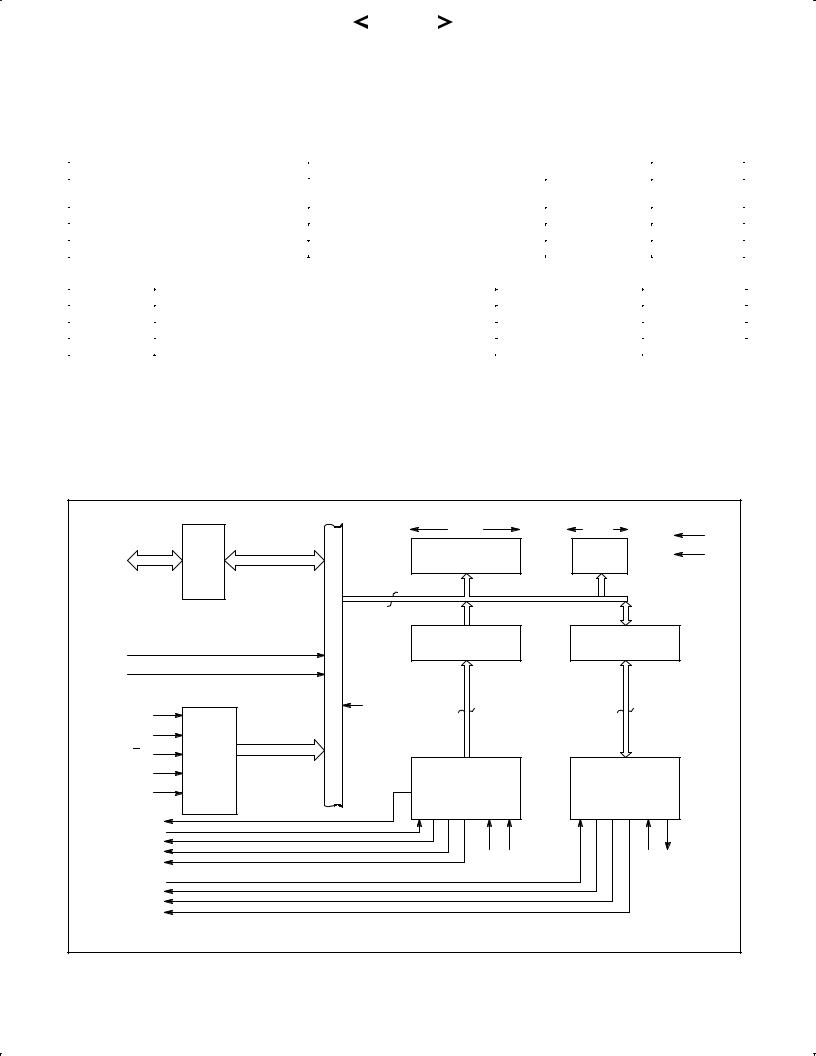
BLOCK DIAGRAM
|
|
|
16 BITS |
|
8 BITS |
|
VCC |
|
|
|
|
|
|
|
|
|
DATA |
|
PARAMETER CONTROL |
PCSAR |
PARAMETER |
PCR |
GND |
DB15± |
|
SYNC/ADDRESS |
CONTROL |
||||
BUS |
|
||||||
|
|
||||||
DB00 |
BUFFER |
|
REGISTER |
|
REGISTER |
|
|
|
|
16 |
|
|
|
|
|
|
|
|
RECEIVER |
RDSR |
TRANSMITTER |
TDSR |
|
|
|
|
DATA/STATUS |
DATA/STATUS |
|||
RESET |
|
|
REGISTER |
|
REGISTER |
|
|
|
|
|
|
|
|
|
|
MM |
|
|
|
|
|
|
|
|
|
INTERNAL |
16 |
|
|
16 |
|
A2±A0 |
|
BUS |
|
|
|
||
|
|
|
|
|
|
||
|
|
|
|
|
|
|
|
BYTE |
|
|
|
|
|
|
|
|
READ/ |
|
|
|
|
|
|
R/W |
WRITE |
|
|
|
|
|
|
|
LOGIC |
|
|
|
|
|
|
CE |
AND |
|
|
|
|
|
|
|
CONTROL |
|
RECEIVER |
|
TRANSMITTER |
|
|
DBEN |
|
|
LOGIC AND |
|
LOGIC AND |
|
|
|
|
CONTROL |
|
CONTROL |
|
||
|
|
|
|
|
|||
S/F |
|
|
|
|
|
|
|
RxE |
|
|
|
|
|
|
|
RxA |
|
|
|
|
|
|
|
RxDA |
|
|
RxC RxSI |
|
|
TxC TxSO |
|
RxSA |
|
|
|
|
|
||
|
|
|
|
|
|
|
|
TxE |
|
|
|
|
|
|
|
TxA |
|
|
|
|
|
|
|
TxBE |
|
|
|
|
|
|
|
TxU |
|
|
|
|
|
|
|
|
|
|
|
|
|
|
SD00058 |
Figure 2. Block Diagram
1995 May 01 |
3 |

Philips Semiconductors |
Product specification |
|
|
|
|
Multi-protocol communications controller (MPCC) |
SCN2652/SCN68652 |
|
|
|
|
PIN DESCRIPTION
|
MNEMONIC |
PIN NO. |
TYPE |
NAME AND FUNCTION |
||||||
|
|
|
|
|
|
|
|
|
|
|
|
|
|
17±10 |
|
Data Bus: DB07±DB00 contain bidirectional data while DB15±DB08 contain control and status |
|||||
DB15±DB00 |
I/O |
information to or from the processor. Corresponding bits of the high and low order bytes can be wire |
||||||||
24±31 |
||||||||||
|
|
|
|
OR'ed onto an 8-bit bus. The data bus is floating if either CE or DBEN are low. |
||||||
|
|
|
|
|
||||||
|
|
|
|
|
|
|
|
|
|
|
A2±A0 |
19±21 |
I |
Address Bus: A2±A0 select internal registers. The four 16-bit registers can be addressed on a word or |
|||||||
byte basis. See Register Address section. |
||||||||||
|
|
|
|
|
||||||
|
|
|
|
|
|
|
|
|
|
|
BYTE |
22 |
I |
Byte: Single byte (8-bit) data bus transfers are specified when this input is high. A low level specifies |
|||||||
16-bit data bus transfers. |
||||||||||
|
|
|
|
|
||||||
|
|
|
|
|
|
|
|
|
|
|
CE |
1 |
I |
Chip Enable: A high input permits a data bus operation when DBEN is activated. |
|||||||
|
|
|
|
|
|
|
|
|
|
|
|
|
|
|
|
Read/Write: |
|
|
|
|
|
|
|
|
|
|
R/W controls the direction of data bus transfer. When high, the data is to be loaded into the |
|||||
|
R/W |
18 |
I |
addressed register. A low input causes the contents of the addressed register to be presented on the |
||||||
|
|
|
|
|
data bus. |
|||||
|
|
|
|
|
|
|
||||
|
|
|
|
|
Data Bus Enable: After A2±A0, CE, BYTE and |
|
|
|||
|
|
|
|
|
R/W are set up, DBEN may be strobed. During a read, |
|||||
DBEN |
23 |
I |
the 3-state data bus (DB) is enabled with information for the processor. During a write, the stable data is |
|||||||
|
|
|
|
|
loaded into the addressed register and TxBE will be reset if TDSR was addressed. |
|||||
|
|
|
|
|||||||
RESET |
33 |
I |
Reset: A high level initializes all internal registers (to zero) and timing. |
|||||||
|
|
|
|
|
|
|||||
MM |
40 |
I |
Maintenance Mode: MM internally gates TxSO back to RxSI and TxC to RxC for off line diagnostic |
|||||||
purposes. The RxC and RxSI inputs are disabled and TxSO is high when MM is asserted. |
||||||||||
|
|
|
|
|
||||||
|
|
|
|
|
|
|||||
RxE |
8 |
I |
Receiver Enable: A high level input permits the processing of RxSI data. A low level disables the |
|||||||
receiver logic and initializes all receiver registers and timing. |
||||||||||
|
|
|
|
|
||||||
|
|
|
|
|
|
|||||
|
|
|
|
|
Receiver Active: RxA is asserted when the first data character of a message is ready for the processor. |
|||||
|
|
|
|
|
In the BOP mode this character is the address. The received address must match the secondary station |
|||||
RxA |
5 |
O |
address if the MPCC is a secondary station. In BCP mode, if strip-SYNC (PCSAR13) is set, the first |
|||||||
|
|
|
|
|
non-SYNC character is the first data character; if strip-SYNC is zero, the character following the second |
|||||
|
|
|
|
|
SYNC is the first data character. In the BOP mode, the closing FLAG resets RxA. In the BCP mode, RxA |
|||||
|
|
|
|
|
is reset by a low level at RxE. |
|||||
|
|
|
|
|||||||
RxDA* |
6 |
O |
Receiver Data Available: RxDA is asserted when an assembled character is in RDSRL and is ready to |
|||||||
|
|
|
|
|
be presented to the processor. This output is reset when RDSRL is read. |
|||||
RxC |
2 |
I |
Receiver Clock: RxC (1X) provides timing for the receiver logic. The positive going edge shifts serial |
|||||||
data into the RxSR from RxSI. |
||||||||||
|
|
|
|
|
||||||
|
|
|
|
|||||||
S/F |
4 |
O |
SYNC/FLAG: S/F is asserted for one RxC clock time when a SYNC or FLAG character is detected. |
|||||||
|
|
|
|
|||||||
RxSA* |
7 |
O |
Receiver Status Available: RxSA is asserted when there is a zero to one transition of any bit in RDSRH |
|||||||
|
|
|
|
|
except for RSOM. It is cleared when RDSRH is read. |
|||||
RxSI |
3 |
I |
Receiver Serial Input: RxSI is the received serial data. Mark = `1', space = `0'. |
|||||||
|
|
|
|
|
|
|||||
|
|
|
|
|
Transmitter Enable: A high level input enables the transmitter data path between TDSRL and TxSO. At |
|||||
TxE |
37 |
I |
the end of a message, a low level input causes TxSO = 1(mark) and TxA = 0 after the closing FLAG |
|||||||
|
|
|
|
|
(BOP) or last character (BCP) is output on TxSO. |
|||||
|
|
|
|
|||||||
TxA |
34 |
O |
Transmitter Active: TxA is asserted after TSOM (TDSR8) is set and TxE is raised. This output will reset |
|||||||
|
|
|
|
|
when TxE is low and the closing FLAG (BOP) or last character (BCP) has been output on TxSO. |
|||||
|
|
|
|
|
|
|||||
TxBE* |
35 |
O |
Transmitter Buffer Empty: TxBE is asserted when theTDSR is ready to be loaded with new control |
|||||||
information or data. The processor should respond by loading theTDSR which resets TxBE. |
||||||||||
|
|
|
|
|
||||||
|
|
|
|
|
|
|||||
|
|
|
|
|
Transmitter Underrun: TxU is asserted during a transmit sequence when the service of TxBE has been |
|||||
TxU* |
36 |
O |
delayed for one character time. This indicates the processor is not keeping up with the transmitter. Line |
|||||||
fill depends on PCSAR11. TxU is reset by RESET or setting of TSOM (TDSR8), synchronized by the |
||||||||||
|
|
|
|
|
||||||
|
|
|
|
|
falling edge of TxC. |
|||||
|
|
|
|
|
|
|||||
TxC |
39 |
I |
Transmitter Clock: TxC (1X) provides timing for the transmitter logic. The positive going edge shifts |
|||||||
data out of the TxSR to TxSO. |
||||||||||
|
|
|
|
|
||||||
|
|
|
|
|||||||
TxSO |
38 |
O |
Transmitter Serial Output: TxSO is the transmitted serial data. Mark = `1', space = `0'. |
|||||||
|
|
|
|
|||||||
VCC |
32 |
I |
+5V: Power supply. |
|||||||
GND |
9 |
I |
Ground: 0V reference ground. |
|||||||
|
|
|
|
|
|
|
|
|
|
|
*Indicates possible interrupt signal
1995 May 01 |
4 |
Philips Semiconductors |
Product specification |
|
|
|
|
Multi-protocol communications controller (MPCC) |
SCN2652/SCN68652 |
|
|
|
|
Table 1. |
Register Access |
|
|
|
|
|
|
|
REGISTERS |
NO. OF BITS |
DESCRIPTION* |
|
|
|
|
Addressable |
|
|
|
|
|
|
|
|
Parameter control sync/ |
|
PCSARH and PCR contain parameters common to the |
PCSAR |
address register |
16 |
receiver and transmitter. PCSARL contains a programmable |
|
|
|
SYNC character (BCP) or secondary station address (BOP). |
PCR |
Parameter control register |
8 |
RDSRH contains receiver status information. |
RDSR |
Receive data/status register |
16 |
RDSRL = RxDB contains the received assembled character. |
|
|
|
TDSRH contains transmitter command and status |
TDSR |
Transmit data/status register |
16 |
information. TDSRL = TxDB contains the character to be |
|
|
|
transmitted |
|
|
|
|
Non-Addressable |
|
|
|
CCSR |
Control character shift register |
8 |
|
|
|
|
|
HSR |
Holding shift register |
16 |
|
|
|
|
|
RxSR |
Receiver shift register |
8 |
|
|
|
|
|
TxSR |
Transmitter shift register |
8 |
|
|
|
|
|
RxCRC |
Receiver CRC accumulation |
16 |
|
register |
|||
|
|
||
|
|
|
|
TxCRC |
Transmitter CRC generation |
16 |
|
register |
|||
|
|
||
|
|
|
These registers are used for character assembly (CSSR, HSR, RxSR), disassembly (TxSR), and CRC accumulation/generation (RxCRC, TxCRC).
NOTES:
*H = High byte ± bits 15±8
L = Low byte ± bits 7±0
Table 2. |
Error Control |
|
CHARACTER |
DESCRIPTION |
|
|
|
|
FCS |
|
Frame check sequence is transmitted/received |
|
|
as 16 bits following the last data character of a |
|
|
BOP message. The divisor is usually |
|
|
CRC±CCITT (X16 + X12 + X5 + 1) with dividend |
|
|
preset to 1's but can be other wise determined |
|
|
by ECM. The inverted remainder is transmitter as |
|
|
the FCS. |
|
|
|
BCC |
|
Block check character is transmitted/received as |
|
|
two successive characters following the last data |
|
|
character of a BCP message. The polynomial is |
|
|
CRC±16 (X16 + X15 + X2 + 1) or CRC±CCITT |
|
|
with dividend preset to 0's (as specified by |
|
|
ECM). The true remainder is transmitted as the |
|
|
BCC. |
Table 3. |
Special Characters |
||
OPERATION |
|
BIT PATTERN |
FUNCTION |
|
|
|
|
BOP |
|
|
|
|
|
|
|
FLAG |
|
01111110 |
Frame message |
|
|
|
|
ABORT |
|
11111111 generation |
Terminate communication |
|
|
|
|
|
|
01111111 detection |
|
|
|
|
|
GA |
|
01111111 |
Terminate loop mode |
|
repeater function |
||
|
|
|
|
|
|
|
|
Address |
|
(PCSAR )1 |
Secondary station address |
|
|
L |
|
BCP |
|
|
|
|
|
|
|
SYNC |
|
(PCSARL) or |
Character synchronization |
|
|
(TxDB)2 generation |
|
NOTES: |
|
|
|
1.( ) = contents of.
2.For IDLE = 0 or 1 respectively.
|
15 |
|
14 |
13 |
|
12 |
11 |
10 |
9 |
8 |
7 |
6 |
5 |
4 |
3 |
2 |
1 |
0 |
|||
PCSAR |
APA |
PROTO |
SS/GA |
|
SAM |
IDLE |
|
E C M |
|
|
|
S/AR |
|
|
|
||||||
|
|
|
|
|
|
|
|
|
|
|
|
|
|
|
|
|
|
|
|
|
|
|
15 |
|
14 |
13 |
|
12 |
11 |
10 |
9 |
8 |
|
|
|
|
|
|
|
|
|||
PCR |
|
TxCL |
|
|
TxC |
R x C |
L E |
|
RxCL |
|
|
|
|
|
|
|
|
||||
|
|
|
|
|
|
|
LE |
|
|
|
|
|
|
|
|
|
|
|
|
|
|
|
15 |
14 |
13 |
12 |
|
11 |
10 |
9 |
|
8 |
|
|
|
|
|
|
|
|
|||
RDSR |
RERR |
|
A B C |
|
|
ROR |
RAB/ |
|
REOM |
|
RSOM |
|
|
|
RxDB |
|
|
|
|||
|
|
|
GA |
|
|
|
|
|
|
|
|
||||||||||
|
|
|
|
|
|
|
|
|
|
|
|
|
|
|
|
|
|
|
|
||
|
15 |
14 |
13 |
12 |
|
11 |
10 |
9 |
|
8 |
|
|
|
|
|
|
|
|
|||
TDSR |
TERR |
NOT DEFINED |
|
|
TGA |
TABORT |
TEOM |
|
TSOM |
|
|
|
TxDB |
|
|
|
|||||
|
|
|
|
|
|
|
|
|
|
|
|
|
|
|
|
|
|
|
|
|
|
NOTE:
Refer to Register Formats for mnemonics and description.
SD00059
Figure 3. Short Form Register Bit Formats
1995 May 01 |
5 |

Philips Semiconductors |
Product specification |
|
|
|
|
Multi-protocol communications controller (MPCC) |
SCN2652/SCN68652 |
|
|
|
|
|
|
|
|
|
|
BCP . CRC |
|
TO |
|
|
|
|
|
|
BOP . CRC |
|
RDSRL |
|
|
|
|
|
|
|
|
|
|
|
|
|
|
|
BCP . CRC |
|
|
|
|
|
|
|
8 |
8 |
|
|
RxSI |
M |
SYNC |
|
|
|
|
M |
|
|
|
|
|
|
|
|||
|
U |
CCSR (8) |
|
|
HSR (16) |
U |
RxSR (8) |
|
|
FF |
|
|
|||||
|
X |
|
|
|
|
X |
|
|
|
|
|
|
|
|
|
||
|
SEL |
1-BIT |
|
|
|
BOP . CRC |
|
|
|
|
DELAY |
SYNC/FLAG1 |
|
ZERO (BOP) |
ZERO |
|
|
FROM |
|
|
|
|
|
|||
|
|
|
DELETION |
DELETION |
|
|
||
|
|
COMPARATOR |
|
|
|
|||
XMITTER |
|
|
|
LOGIC |
CONTROL |
|
|
|
|
|
|
|
|
|
|||
MM |
|
|
|
|
PARITY (BCP) |
|
|
|
|
|
|
|
|
|
|
|
|
|
|
|
|
BOP |
LOGIC |
|
|
|
|
|
|
|
|
|
|
|
|
S/F |
|
|
|
M |
|
CRC±16 (BCP) OR |
CRC±16 = 0 |
RERR |
|
|
|
|
|
||||
|
|
|
BCP |
U |
RxCRC ACC |
CCRC±CCITT |
COMPARATOR |
|
|
|
|
|
X |
|
(BOP) |
CRC±CCIT = F0B8 |
|
|
|
|
|
|
RESET |
|
|
|
|
|
|
|
|
RxE |
RECEIVER |
|
|
|
|
|
|
|
RxA |
CONTROL |
|
|
|
|
|
|
|
RxDA |
LOGIC |
|
|
|
|
|
|
|
RxSA |
|
|
|
RxC
NOTES:
1.Detected in SYNC FF and 7 MS bits of CCSR.
2.In BOP mode, a minimum of two data characters must be received to turn the receiver active.
|
|
|
|
|
SD00060 |
|
|
Figure 4. MPCC Receiver Data Path |
|
|
|
|
|
FROM OR PCSARL (SYNC) |
|
|
|
|
|
TDSARL |
|
|
|
RESET |
|
|
|
|
|
TxE |
|
|
|
SYNC |
|
TRANS- |
TXSR (8) |
|
FF |
TxSO |
|
|
|
|
|
||
|
MITTER |
|
|
|
|
TxA |
|
|
|
|
|
CONTROL |
|
|
1 BIT |
|
|
|
|
|
|
||
|
LOGIC |
|
|
|
|
TxBE |
|
|
DELAY |
|
|
|
|
|
|
||
TxU |
|
|
|
|
|
|
|
|
M |
BOP |
|
|
|
|
ZERO |
|
|
|
|
|
U |
|
|
|
|
|
INSERTION |
|
|
|
|
TXCRC ACC (16) |
X |
ZERO |
|
|
|
LOGIC |
|||
|
|
CRC±16 OR CRC±CCITT |
|
INSERTION |
|
|
|
|
|
||
|
|
|
|
|
CONTROL |
|
|
|
|
BCP |
|
|
|
|
SEL1, 2 |
PARITY |
|
|
TxC |
|
|
GENERATION |
|
|
|
|
|
|
|
|
|
CONTROL |
|
|
|
|
|
CHARACTER |
|
|
|
|
|
GENERATOR |
|
|
|
|
FLAG ABORT GA |
|
NOTES: |
|
|
1. |
TxCRC selected if TEOM = 1 and the last data character has been shifted out of TxSR. |
|
2. |
In BCP parity selected will be generated after each character is shifted out of TxSR. |
SD00088 |
|
|
|
Figure 5. MPCC Transmitter Data Path
1995 May 01 |
6 |

Philips Semiconductors |
Product specification |
|
|
|
|
Multi-protocol communications controller (MPCC) |
SCN2652/SCN68652 |
|
|
|
|
FUNCTIONAL DESCRIPTION
The MPCC can be functionally partitioned into receiver logic, transmitter logic, registers that can be read or loaded by the processor, and data bus control circuitry. The register bit formats are shown in Figure 3 while the receiver and transmitter data paths are depicted in Figures 4 and 3.
RECEIVER OPERATION
General
After initializing the parameter control registers (PCSAR and PCR), the RxE input must be set high to enable the receiver data path. The serial data on the RxSI is synchronized and shifted into an 8-bit Control Character Shift Register (CCSR) on the rising edge of RxC. A comparison between CCSR contents and the FLAG (BOP) or SYNC (BCP) character is made until a match is found. At that time, the S/F output is asserted for one RxC time and the 16-bit Holding
Shift Register (HSR) is enabled. The receiver then operates as described below.
should check RDSR9±15 each time RxSA is asserted. If RDSR9 is set, then RDSR12±15 should be examined.
Receiver character length may be changed dynamically in response to RxDA: read the character in RxDB and write the new character length into RxCL. The character length will be changed on the next receiver character boundary. A received residual (short) character will be transferred into RxDB after the previous character in RxDB has been read, i.e. there will not be an overrun. In general the last two characters are protected from overrun.
The CRC±CCITT, if specified by PCSAR8±10, is accumulated in RxCRC on each character following the FLAG. When the closing FLAG is detected in the CCSR, the received CRC is in the 16-bit
HSR. At that time, the Receive End of Message bit (REOM) will be set; RxSA and RxDA will be asserted. The processor should read the last data character in RDSRL and the receiver status in
RDSR9±15. If RDSR15 = 1, there has been a transmission error; the accumulated CRC±CCITT is incorrect. If RDSR12±14 ≠ 0, last data character is not of prescribed length. Neither the received CRC nor
closing FLAG are presented to the processor. The processor may drop RxE or leave it active at the end of the received message.
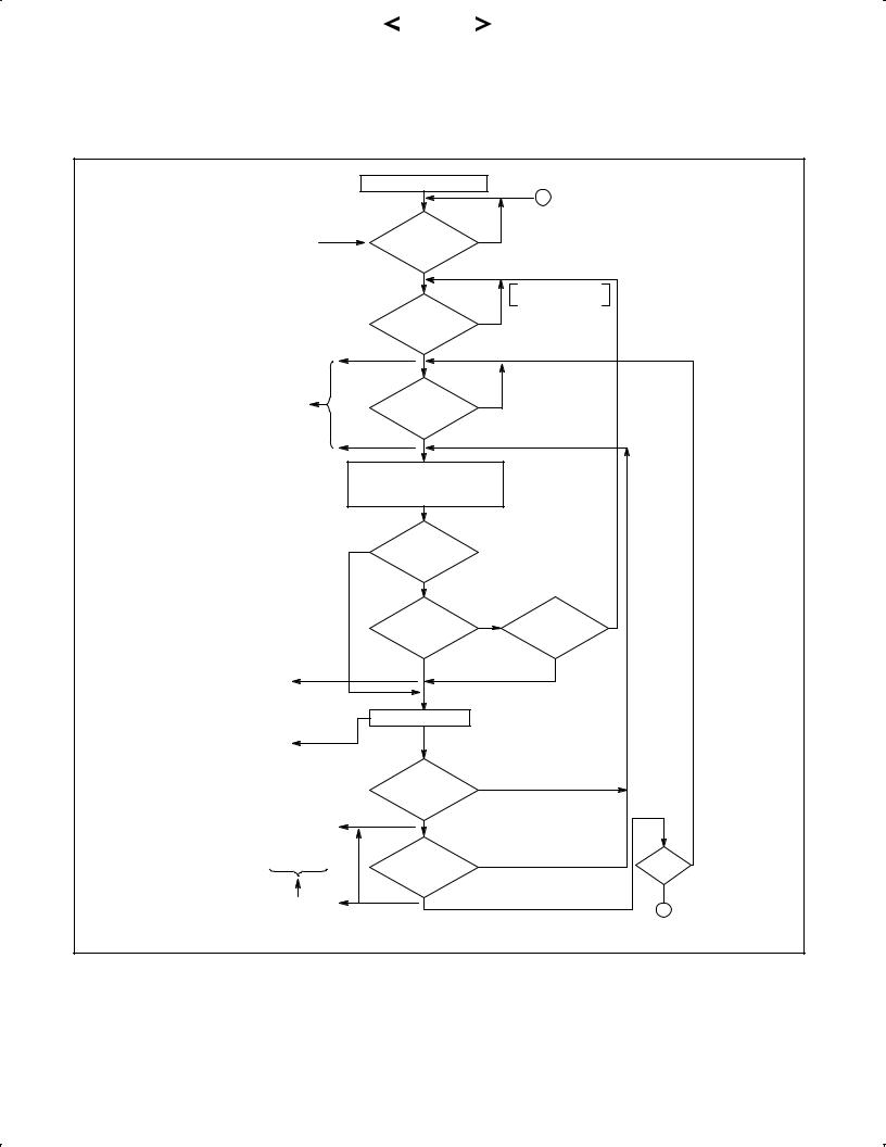
BOP Operation
A flowchart of receiver operation in BOP mode appears in Figure 6. Zero deletion (after five ones are received) is implemented on the received serial data so that a data character will not be interpreted as a FLAG, ABORT, or GA. Bits following the FLAG are shifted through the CCSR, HSR, and into the Receiver Shift Register (RxSR). A character will be assembled in the RxSR and transferred to the RDSRL for presentation to the processor. At that time the RxDA output will be asserted and the processor must take the character no later than one RxC time after the next character is assembled in the RxSR. If not, an overrun (RDSR11 = 1) will occur and succeeding characters will be lost.
The first character following the FLAG is the secondary station address. If the MPCC is a secondary station (PCSAR12 = 1), the contents of RxSR are compared with the address stored in PCSARL. A match indicates the forthcoming message is intended for the station; the RxA output is asserted, the character is loaded into RDSRL, RxDA is asserted and the Receive Start of Message bit (RSOM) is set. No match indicates that another station is being addressed and the receiver searches for the next FLAG.
If the MPCC is a primary station, (PCSAR12 = 0), no secondary address check is made; RxA is asserted and RSOM is set once the first non-FLAG character has been loaded into RDSRL and RxDA has been asserted. Extended address field can be supported by software if PCSAR12 = 0.
When the 8 bits following the address character have been loaded into RDSRL and RxDA has been asserted, RSOM will be cleared.
The processor should read this 8-bit character and interpret it as the Control field.
Received serial data that follows is read and interpreted as the information field by the processor. It will be assembled into character
lengths as specified by PCR8±10. As before, RxDA is asserted each time a character has been transferred into RDSRL and is cleared
when RDSRL is read by the processor. RDSRH should only be read when RxSA is asserted. This occurs on a zero to one transition of any bit in RDSRH except for RSOM. RxSA and all bits in RDSRH except RSOM are cleared when RDSRH is read. The processor
RxBCP Operation
The operation of the receiver in BCP mode is shown in Figure 7.
The receiver initially searches for two successive SYNC characters,
of length specified by PCR8±10, that match the contents of PCSARL. The next non-SYNC character or next SYNC character, if stripping is
not specified (PCSAR13 = 0), causes RxA to be asserted and enables the receiver data path. Once enabled, all characters are assembled in RxSR and loaded into RDSRL. RxDA is active when a character is available in RDSRL. RxSA is active on a 0 to 1 transition of any bit in RDSRH. The signals are cleared when RDSRl or RDSRH are read respectively.
If CRC±16 error control is specified by PCSAR8±10, the processor must determine the last character received prior to the CRC field. When that character is loaded into RDSRL and RxDA is asserted, the received CRC will be in CCSR and HSRL. To check for a transmission error, the processor must read the receiver status
(RDSRH) and examine RDSR15. This bit will be set for one character time if an error free message has been received. If RDSR15 = 0, the CRC±16 is in error. The state of RDSR15 in BCP CRC mode does not set RxSA. Note that this bit should be examined only at the end of a message. The accumulated CRC will include all characters starting with the first non-SYNC character if PCSAR13 = 1, or the character after the opening two SYNCs if PCSAR13 = 0. This necessitates external CRC generation/checking when supporting IBM's
BISYNC. This can be accomplished using the Philips Semiconductors SCN2653 Polynomial Generator/Checker. See
Typical Applications.
If VRC has been selected for error control, parity (odd or even) is regenerated on each character and checked when the parity bit is received. A discrepancy causes RDSR15 to be set and RxSA to be asserted. This must be sensed by the processor. The received parity bit is stripped before the character is presented to the processor.
When the processor has read the last character of the message, it should drop RxE which disables the receiver logic and initializes all receiver registers and timing.
1995 May 01 |
7 |
Philips Semiconductors |
Product specification |
|
|
|
|
Multi-protocol communications controller (MPCC) |
SCN2652/SCN68652 |
|
|
|
|
PROCESSOR |
|
INITIALIZE PCSAR, PCR |
|
|
|
|
|
|
|
|
|
A |
|
|
|
|
|
|
|
|
|
|
|
RxE = 1 |
|
RxE |
|
|
|
|
|
|
= 1? |
|
NO |
|
|
|
|
|
|
|
|
|
|
||
|
|
YES |
|
|
|
|
|
|
|
|
|
|
* TEST MADE |
|
|
|
|
|
|
|
EVERY RxC TIME |
|
|
|
|
FLAG |
|
NO |
|
|
|
|
|
IN CCSR* |
|
|
|
|
|
|
|
|
|
|
|
|
|
|
|
? |
|
|
|
|
|
|
|
YES |
|
|
|
|
|
S/F = 1 |
|
FLAG |
|
YES |
|
|
|
FOR ONE RxC |
|
|
|
|
|
||
BIT TIME |
|
IN CCSR* |
|
|
|
|
|
|
? |
|
|
|
|
|
|
|
|
|
|
|
|
|
|
|
|
NO |
|
|
|
|
|
|
|
ASSEMBLE CHARACTER |
(1) OVERRUN (ROVRN) |
|
|||
|
|
IN RxSR. ZERO DELETION, |
CAUSES LOSS OF |
|
|||
|
|
ACCUMULATE CRC IF |
|
SUBSEQUENT |
|
|
|
|
|
SPECIFIED |
|
|
CHARACTERS |
|
|
|
|
IS |
|
|
|
|
|
|
NO |
IT 1st |
|
|
|
|
|
|
CHARACTER |
|
|
|
|
|
|
|
|
|
|
|
|
|
|
|
|
AFTER FLAG |
|
|
|
|
|
|
|
? |
|
|
|
|
|
|
|
YES |
SECONDARY |
|
|
|
|
|
|
STATION |
|
|
|
||
|
|
|
ADDRESS |
|
|
|
|
|
|
SEC. |
|
|
IS |
NO |
|
|
|
STATION |
|
|
CHARACTER |
|
|
|
|
MODE |
|
YES |
= PCSARL |
|
|
|
|
? |
(PCSAR12 = 1) |
? |
|
|
|
START OF |
|
NO |
|
|
|
||
|
|
|
YES |
|
|
||
MESSAGE |
|
(PCSAR12 = 0) |
|
|
|||
|
|
|
|
||||
RxA = 1 |
|
|
|
|
|
|
|
RSOM = 1 |
|
|
|
|
|
|
|
FOR ONE |
|
|
|
|
|
|
|
CHARACTER |
|
RxSR → RxDB |
|
|
|
|
|
TIME |
|
|
|
|
|
|
|
RxDA = 1 |
|
|
|
|
|
|
|
(PROCESSOR |
|
|
|
|
|
|
|
SHOULD |
|
|
|
|
|
|
|
READ RxDB) |
|
RECEIVER |
|
|
|
|
|
|
|
|
|
|
|
|
|
|
|
STATUS BIT 0 → 1 |
NO |
|
|
|
|
|
|
EXCEPT RSOM |
|
|
|
|
|
RXSA = 1 |
|
? |
|
|
|
|
|
|
|
|
|
|
|
|
|
(PROCESSOR SHOULD |
|
YES |
|
|
|
|
|
READ AND EXAMINE |
|
|
|
|
|
|
|
RDSRH ± REOM, RAB/GA, |
|
FLAG |
|
|
|
|
|
ROVRN, ABC, RERR) |
|
|
|
|
RxE → 0 |
|
|
|
|
IN CCSR* |
|
NO |
|
|
|
|
|
|
|
? |
NO |
||
|
|
? |
|
|
|||
|
|
|
|
|
|
||
S/F = 1 FOR ONE RxC |
|
YES ± END OF MESSAGE |
YES |
|
|||
|
A |
|
|||||
BIT TIME |
|
|
|
|
|
|
|
|
|
|
|
|
|
|
|
REOM = 1, RxA = 0 |
|
|
|
|
|
|
|
|
|
|
|
|
|
SD00061 |
|
Figure 6. BOP Receive
TRANSMITTER OPERATION General
After the parameter control registers (PCSAR and PCR) have been initialized, TxSO is held at mark until TSOM (TDSR8) is set and TxE is raised. Then, transmitter operation depends on protocol mode.
TxBOP Operation
Transmitter operation for BOP is shown in Figure 8. A FLAG is sent after the processor sets the Transmit Start of Message bit (TSOM) and raises TxE. The FLAG is used to synchronize the message that follows. TxA will also be asserted. When TxBE is asserted by the
1995 May 01 |
8 |

Philips Semiconductors |
Product specification |
|
|
|
|
Multi-protocol communications controller (MPCC) |
SCN2652/SCN68652 |
|
|
|
|
MPCC, the processor should load TDSRL with the first character of the message. TSOM should be cleared at the same time TDSRL is loaded (16-bit data bus) or immediately thereafter (8-bit data bus). FLAGS are sent as long as TSOM = 1. For counting the number of
FLAGs, the processor should reassert TSOM in response to the assertion of TxBE.All succeeding characters are loaded into TDSRL by the processor when TxBE = 1. Each
character is serialized in TxSR and transmitted on TxSO. Internal zero insertion logic stuffs a ª0º into the serial bit stream after five successive ª1sº are sent. This insures a data character will not match a FLAG, ABORT, or GA reserved control character. As each character is transmitted, the Frame Check Sequence (FCS) is generated as specified by Error Control Mode (PCSAR8±10). The
FCS should be the CRC±CCITT polynomial (X16 + X12 + X5 + 1) preset to 1s. If an underrun occurs (processor is not keeping up with the transmitter), TxU and TERR (TDSR15) will be asserted with ABORT or FLAG used as the TxSO line fill depending on the state of IDLE (PCSAR11). The processor must set TSOM to reset the underrun condition. To retransmit the message, the processor should proceed with the normal start of message sequence.
A residual character of 1 to 7 bits may be transmitted at the end of the information field. In response to TxBE, write the residual character length into TxCL and load TxDB with the residual character. Dynamic alteration of character length should be done in exactly the same sequence. The character length will be changed on the next transmit character boundary.
After the last data character has been loaded into TDSRL and sent to TxSR (TxBE = 1), the processor should set TEOM (TDSR9). The MPCC will finish transmitting the last character followed by the FCS and the closing FLAG. The processor should clear TEOM and drop
TxE when the next TxBE is asserted. This corresponds to the start of closing FLAG transmission. When TxE has been dropped. TxA will be low 1 1/2 bit times after the last bit of the closing FLAG has been transmitted. TxSO will be marked after the closing FLAG has been transmitted.
If TxE and TEOM are high, the transmitter continues to send
FLAGs. The processor may initiate the next message by resetting TEOM and setting TSOM, or by loading TDSRL with a data character and then simply resetting TSOM (without setting TSOM).
TxBCP Operation
Transmitter operation for BCP mode is shown in Figure 9. TxA will be asserted after TSOM = 1 and TxE is raised. At that time SYNC characters are sent from PCSARL or TDSRL (IDLE = 0 or 1) as long as TSOM = 1. TxBE is asserted at the start of transmission of the first SYNC character. For counting the number of SYNCs, the processor should reassert TSOM in response to the assertion of TxBE. When TSOM = 0 transmission is from TDSRL, which must be loaded with characters from the processor each time TxBE is asserted. If this loading is delayed for more than one character time, an underrun results: TxU and TERR are asserted and the
TxSO line fill depend on IDLE (PCSAR11). The processor must set TSOM and retransmit the message to recover. This is not compatible with IBM's BISYNC, so that the user must not underrun when supporting that protocol.
CRC±16, if specified by PCSAR8±10, is generated on each character transmitted from TDSRL when TSOM =0. The processor must set TEOM = 1 after the last data character has been sent to TxSR (TxBE = 1). The MPCC will finish transmitting the last data character and the CRC±16 field before sending SYNC characters which are transmitted as long as TEOM = 1. If SYNCs are not desired after CRC±16 transmission, the processor should clear TEOM and lower TxE when the TxBE corresponding to the start of CRC±16 transmission is asserted. When TEOM = 0, the line is marked and a new message may be initiated by setting TSOM and raising TxE.
If VRC is specified, it is generated on each data character and the data character length must not exceed 7 bits. For software LRC or CRC, TEOM should be set only if SYNC's are required at the end of the message block.
SPECIAL CASE: The capability to transmit 16 spaces is provided for line turnaround in half duplex mode or for a control recovery situation. This is achieved by setting TSOM and TEOM, clearing
TEOM when TxBE = 1, and proceeding as required.
PROGRAMMING
Prior to initiating data transmission or reception, PCSAR and PCR must be loaded with control information from the processor. The contents of these registers (see Register Format section) will configure the MPCC for the user's specific data communication environment. These registers should be loaded during power-on initialization and after a reset operation. They can be changed at any time that the respective transmitter or receiver is disabled.
The default value for all registers is zero. This corresponds to BOP, primary station mode, 8-bit character length, FCS = CRC±CCITT preset to 1s.
For BOP mode the character length register (PCR) may be set to the desired values during system initialization. The address and control fields will automatically be 8-bits. If a residual character is to be transmitted, TxCL should be changed to the residual character length prior to transmission of that character.
DATA BUS CONTROL
The processor must set up the MPCC register address (A2±A0), chip enable (CE), byte select (BYTE), and read/write (R/W) inputs before each data bus transfer operation.
During a read operation (R/W = 0), the leading edge of DBEN will initiate an MPCC read cycle. The addressed register will place its contents on the data bus. If BYTE = 1, the 8-bit byte is placed on DB15±08 or DB07±00 depending on the H/L status of the register addressed. Unused bits in RDSRL are zero. If BYTE = 0, all 16 bits
(DB15±00) contain MPCC information. The trailing edge of DBEN will reset RxDA and/or RxSA if RDSRL or RDSRH is addressed respectively.
DBEN acts as the enable and strobe so that the MPCC will not begin its internal read cycle until DBEN is asserted.
During a write operation (R/W = 1), data must be stable on DB15±08 and/or DB07±00 prior to the leading edge of DBEN. The stable data is strobed into the addressed register by DBEN. TxBE will be
cleared if the addressed register was TDSRH or TDSRL.
1995 May 01 |
9 |
Loading...