

Philips NE56632-31D, NE56632-43D, NE56632-45D, NE56632-46D, NE56632-30D Datasheet
...
INTEGRATED CIRCUITS
NE56632-XX
Active-LOW system reset
with adjustable delay time
Product data 2002 Mar 25
Philips Semiconductors Product data
NE56632-XXActive-LOW system reset with adjustable delay time
DESCRIPTION
The NE56632-XX is a family of Active-LOW, power-on reset that
offers precision threshold voltage detection within ±1.5% and super
low operating supply current of typically 3.0 µA. It includes a reset
delay that is user adjustable with an external capacitor.
Several detection threshold voltages are available at 1.9V , 2.0 V ,
2.7 V, 2.8 V, 2.9 V, 3.0 V, 3.1 V, 4.2 V, 4.3 V, 4.4 V, 4.5 V, and 4.6 V.
Other thresholds are offered upon request at 100 mV steps from
1.9 V to 4.6 V.
With its ultra low supply current and high precision voltage threshold
detection capability, the NE56632-XX is well suited for various
battery powered applications such as reset circuits for logic and
microprocessors, voltage check, and level detecting. It is available in
the SOT23-5 package.
FEA TURES
•High precision threshold detection voltage: V
±1.5%
S
•Super low operating supply current: 3 µA typ.
•Built-in hysteresis voltage: 50 mV typ.
•Detection threshold voltage: 1.9 V, 2.0 V , 2.7 V, 2.8 V, 2.9 V,
3.0 V, 3.1 V, 4.2 V, 4.3 V, 4.4 V, 4.5 V, and 4.6 V.
•Reset Output: Active-LOW, open collector
•Other detection threshold voltages available upon request at
100 mV steps from 1.9 V to 4.6 V.
•Large low reset output current: 30 mA typ.
•Power-on reset delay time adjustable with external capacitor:
200 µs to 200 ms
•Reset assertion with V
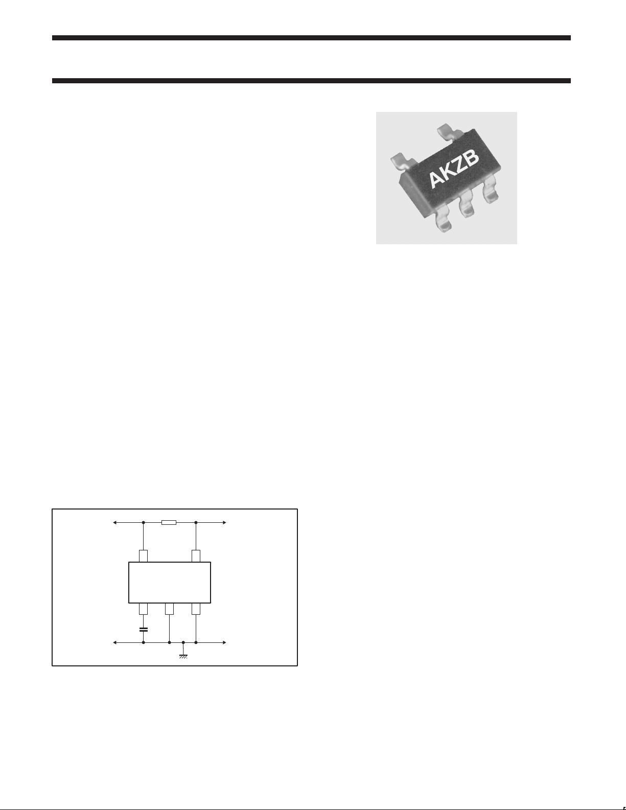
SIMPLIFIED SYSTEM DIAGRAM
TO V
CC
down to 0.65 V
CC
R
PU
NE56632-XX
TO RESET
TERMINAL
OF CPU
45
APPLICATIONS
•Reset for microprocessor and logic circuits
•Voltage level detection circuit
•Battery voltage check circuit
•Detection circuit for battery back-up
123
C
D
SL01605
Figure 1. Simplified system diagram.
2002 Mar 25 853–2329 27919
2
Philips Semiconductors Product data
TYPE NUMBER
NE56632-XXActive-LOW system reset with adjustable delay time
ORDERING INFORMATION
PACKAGE
NAME DESCRIPTION
NE56632-XXD SOT23-5 / SOT25 (SO5) plastic small outline package; 5 leads (see dimensional drawing) –20 to +75 °C
NOTE:
The device has 12 voltage output options, indicated by the XX on
the ‘Type number’.
XX
VOLTAGE (Typical)
19 1.9 V
20 2.0 V
27 2.7 V
28 2.8 V
29 2.9 V
30 3.0 V
31 3.1 V
42 4.2 V
43 4.3 V
44 4.4 V
45 4.5 V
46 4.6 V
Part number marking
The package is marked with a four letter code. The first three letters
designate the product. The fourth letter, represented by ‘x’, is a date
tracking code.
Part Number
NE56632-19D AKZx
NE56632-20D ALAx
NE56632-27D ALBx
NE56632-28D ALCx
NE56632-29D ALDx
NE56632-30D ALEx
NE56632-31D ALFx
NE56632-42D ALGx
NE56632-43D ALHx
NE56632-44D ALJx
NE56632-45D ALKx
NE56632-46D ALLx
Marking
TEMPERATURE
RANGE
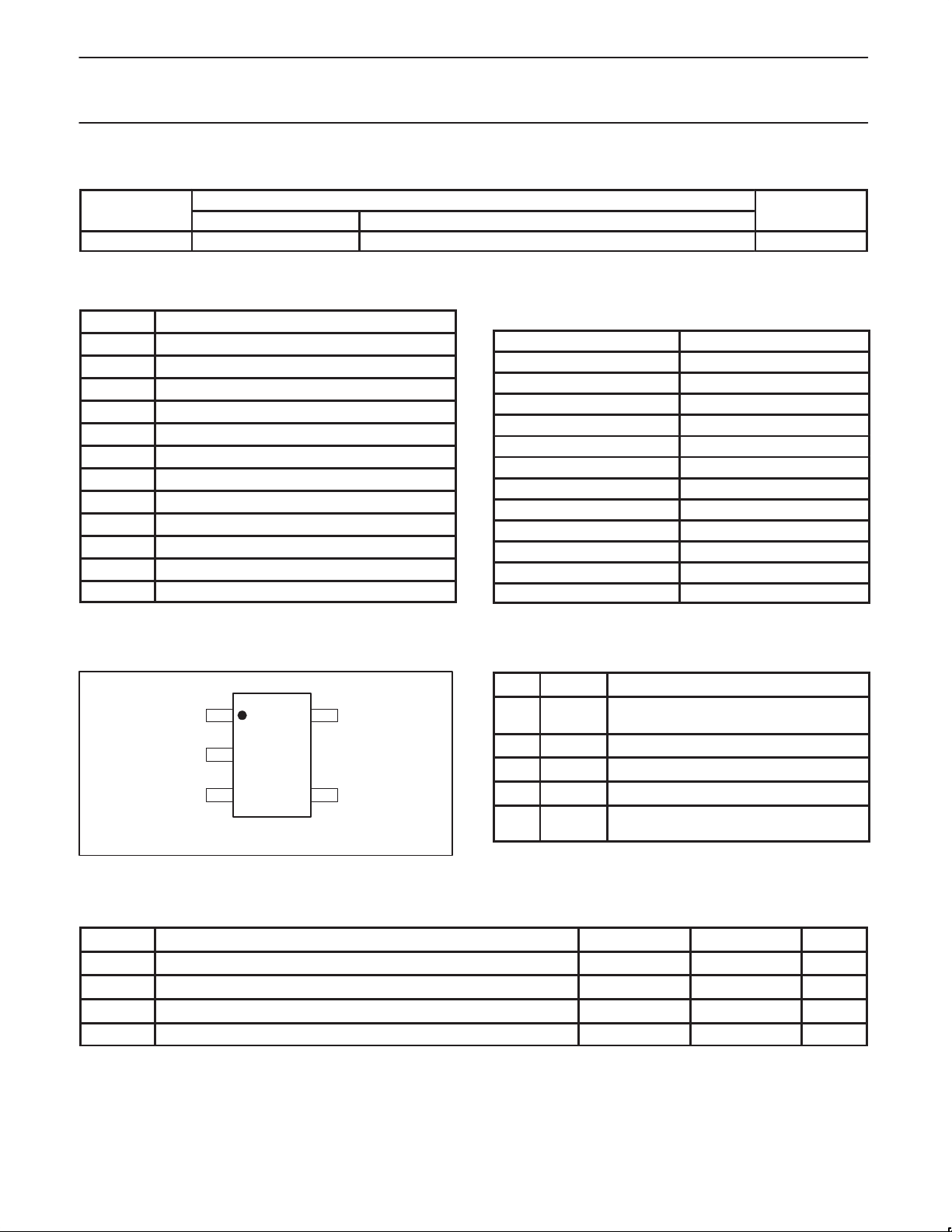
PIN CONFIGURATION
PIN DESCRIPTION
PIN SYMBOL DESCRIPTION
1 TC Delay time control; set with external
capacitor.
2 SUB Substrate. Connect to ground (GND).
SUB
1
TC
2
NE56632-XX
5V
CC
3 GND Ground. Negative supply.
34
GND
SL01604
V
OUT
4 V
5 V
OUT
CC
Reset output voltage. Active-LOW.
Positive supply voltage; detection threshold
voltage input.
Figure 2. Pin configuration.
MAXIMUM RATINGS
SYMBOL PARAMETER MIN. MAX. UNIT
V
CC
T
amb
T
stg
P Power dissipation – 150 mW
Supply voltage –0.3 +10 V
Ambient operating temperature –20 +75 °C
Storage temperature –40 +125 °C
2002 Mar 25
3
Philips Semiconductors Product data
V
(Fig
)
Test Circuit 1 (Figure 27)
NE56632-XXActive-LOW system reset with adjustable delay time
ELECTRICAL CHARACTERISTICS
T
= 25 °C, unless otherwise specified.
amb
SYMBOL
V
S
V
hys
VS/∆T Detection threshold voltage
V
OL
I
LO
I
CCL
I
CCH
t
PLH
t
PHL
V
OPL
I
OL1
I
OL2
NOTES:
1. t
:VCC = (V
PLH
:VCC = (V
2. t
PHL
3. See Table 1.
PARAMETER CONDITIONS -XX MIN. TYP. MAX. UNIT
Detection threshold VCC = HIGH-to-LOW; RL = 4.7 kΩ; S1=ON;
≤ 0.4 V;
OL
Test Circuit 1
ure 27
46
45
44
43
42
31
30
29
28
27
20
19
Hysteresis voltage RL = 4.7 kΩ; VCC = LOW-to-HIGH-to-LOW; S1 = ON; Test
4.531 4.600 4.669 V
4.432 4.500 4.568 V
4.334 4.400 4.466 V
4.235 4.300 4.365 V
4.137 4.200 4.263 V
3.053 3.100 3.147 V
2.955 3.000 3.045 V
2.856 2.900 2.944 V
2.758 2.800 2.842 V
2.659 2.700 2.741 V
1.970 2.000 2.030 V
1.871 1.900 1.929 V
25 50 100 mV
Circuit 1 (Figure 27)
temperature coefficient
LOW-level output voltage V
Output leakage current V
Supply current (ON time) V
Supply current (OFF time) V
CC1
CC1
CC1
RL = 4.7 kΩ; T
= V
CC1
= V
= 10 V; S2 = ON; Test Circuit 1 (Figure 27) – – ±0.1 µA
CC2
= V
S(min)
= V
S(typ)
= –20 °C to +75 °C; S1 = ON;
amb
Test Circuit 1 (Figure 27)
– 0.05 V; RL = 4.7 kΩ; S1 = ON;
S(min)
Test Circuit 1 (Figure 27)
– ±0.01 – %/°C
– 0.2 0.4 V
– 0.05 V; RL = ∞; Test Circuit 1 (Figure 27) – 5.0 9.0 µA
/0.85; RL = ∞; Test Circuit 1 (Figure 27) – 3.0 5.0 µA
LOW-to-HIGH delay time CL = 100 pF; RL = 4.7 kΩ; CD = 10 nF (Note 1) – (Note 3) – ms
HIGH-to-LOW delay time CL = 100 pF; RL = 4.7 kΩ; CD = 10 nF (Note 2) – (Note 3) – µs
Minimum operating
threshold voltage
Output current (ON Time 1) VO = 0.4 V; RL = 0; V
Output current (ON Time 2) VO = 0.4 V; RL = 0; V
– 0.4 V) to (V
S(typ)
+ 0.4 V) to (V
S(typ)
S(typ)
S(typ)
+ 0.4 V); t
– 0.4 V); t
RL = 4.7 kΩ; VOL ≤ 0.4 V; S1 = ON;
Test Circuit 1 (Figure 27)
= V
CC1
CC1
= V
S(min)
S(min)
V
= 0.4 V; S2 = ON; Test Circuit 1 (Figure 27)
CC2
T
= –20 °C to +75 °C; S2 = ON;
amb
Test Circuit 1 (Figure 27)
is release delay time (Test Circuit 2, Figure 28).
PLH
is assertion delay time (Test Circuit 2, Figure 28).
PHL
– 0.05 V;
– 0.05 V;
– 0.65 0.80 V
5 – – mA
3 – – mA
Table 1. NE56632-XX series typical delay time
–XX t
PLH
46 195 ms 140 µs
45 190 ms 140 µs
44 185 ms 140 µs
43 180 ms 140 µs
42 175 ms 140 µs
31 120 ms 120 µs
30 115 ms 120 µs
29 110 ms 120 µs
28 105 ms 100 µs
27 100 ms 100 µs
20 65 ms 100 µs
19 60 ms 100 µs
2002 Mar 25
t
PHL
4

Philips Semiconductors Product data
NE56632-XXActive-LOW system reset with adjustable delay time
TYPICAL PERFORMANCE CURVES, NE56632-20
2.0050
2.0025
2.0000
1.9975
1.9950
1.9925
, DETECTION THRESHOLD (V)
S
V
1.9900
1.9875
1.9850
–40 –20
0 20 40 60 80 100
AMBIENT TEMPERATURE, T
Test Circuit 1
VCC = HIGH-to-LOW
= 4.7 kΩ
R
L
VOL ≤ 0.4 V
S1 = ON
(°C)
amb
SL01620
Figure 3. Detection threshold versus temperature.
0.225
0.220
0.215
0.210
0.205
0.200
, LOW-LEVEL OUTPUT VOLTAGE (V)
V
OL
0.195
0.190
0.185
–40 –20
0 20 40 60 80 100
AMBIENT TEMPERATURE, T
Test Circuit 1
V
= V
CC1
S(min)
RL = 4.7 kΩ
S1 = ON
(°C)
amb
– 0.05 V
SL01622
Figure 5. LOW-level output voltage versus temperature.
100
90
80
70
60
50
, HYSTERESIS VOLTAGE (mV)
Test Circuit 1
hys
VCC = LOW-to-HIGH-to-LOW
V
40
RL = 4.7 kΩ
S1 = ON
30
–40 –20
0 20 40 60 80 100
AMBIENT TEMPERATURE, T
amb
(°C)
SL01621
Figure 4. Hysteresis voltage versus temperature.
9
8
7
6
5
, SUPPLY CURRENT (ON time), ( A)µ
4
Test Circuit 1
CCL
I
V
= V
CC1
= ∞
R
L
3
–40 –20
– 0.05 V
S(min)
0 20 40 60 80 100
AMBIENT TEMPERATURE, T
amb
(°C)
SL01623
Figure 6. Supply current (ON time) versus temperature.
4.5
4.0
3.5
3.0
2.5
, SUPPLY CURRENT (OFF time), ( A)µ
I
CCH
Test Circuit 1
RL = ∞
V
CC1
2.0
–40 –20
= V
/0.85
S(typ)
0 20 40 60 80 100
AMBIENT TEMPERATURE, T
amb
(°C)
Figure 7. Supply current (OFF time) versus temperature.
2002 Mar 25
SL01624
0.9
0.8
0.7
0.6
0.5
Test Circuit 1
0.4
RL = 4.7 kΩ
VOL ≤ 0.4 V
S1 = ON
, MIN. OPERATING THRESHOLD VOLTAGE (V)
0.3
OPL
–40 –20
V
0 20 40 60 80 100
AMBIENT TEMPERATURE, T
amb
(°C)
Figure 8. Min. operating threshold voltage versus temperature.
5
SL01625
 Loading...