

Philips 21PV375-01, 21PV375-07, 21PV375-39, 21PV375-58 Service Manual

TV-VCR Combination
Service
21PV375
/01/07/39/58
Service
Service
Service Manual
Contents
Chapter
Adjustment Procedure
Sec. 1:
Schematic Diagrams and CBA's
Exploded Views
Mechanical and Electrical Parts Lists
Survey of versions:
/01 PAL-BG, EURO
/07 PAL I, UK/IRELAND
/39 PAL/SECAM-BG+PAL/SECAM-L/L',FRANCE
/58 PAL-BG/DK+SECAM-BG/DK,EAST-EURO
Sec. 2:
Standard Maintenance
Mechanism Alignment Procedures
Disassembly / Assembly of Mechanism
Deck Exploded Views
For technical data reference is made to the Service Manual of
14PV374/01/07/39/58 & 14PV375/01/07/39/58 3103 785 22220.
The present Manual states only the differences.
Safety regulations require that the set be restored to its original
condition and that parts which are identical with those specified
be used.
Published by BK 2003 Video Service Department Printed in Japan c
Copyright reserved Subject to modification GB 3103 785 22240
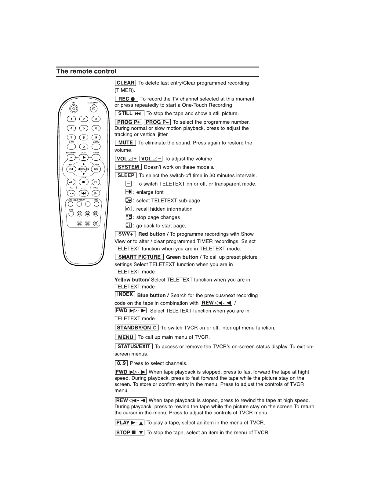
OPERATING CONTROLS AND FUNCTIONS
[ 21PV375/ ( 01, 07, 39, 58 ) ]
1-4-3 T6500IB

1-4-4 T6500IB

CABINET DISASSEMBLY INSTRUCTIONS
[ 21PV375/ ( 01, 07, 39, 58 ) ]
1. Disassembly Flowchart
This flowchart indicates the disassembly steps for the
cabinet parts, and the CBA in order to gain access to
item(s) to be serviced. When reassembling, follow the
steps in reverse order. Bend, route and dress the
cables as they were.
Caution !!
When removing the CRT, be sure to discharge the
Anode Lead of the CRT with the CRT Ground Wire
before removing the Anode Cap.
[1] Rear Cabinet
[2] Power Unit and Tray Chassis Unit
[5] H.V./Power
Supply CBA
[3] Power Unit
[4] Tray Chassis Unit
[6] Top Shield
[7] Bottom Plate
[8] Deck Unit
REMOVAL
ID/
LOC.
No.
[5]
[6] Top Shield 3 5(S-4), CL604 5
[7]
[8] Deck Unit 3, 5
[9] Text CBA 3, 5
[10] Main CBA 3 4(S-10) 9
[11] CRT 4 4(S-11) 10
↓
(1)
PAR T
H.V./Power
Supply
CBA
Bottom
Plate
↓
(2)
REMOVE/
*UNHOOK/
Fig.
UNLOCK/RELEASE/
No.
UNPLUG/DESOLDER
36(S-3) 4
3(S-5) 6
7(S-6), (S-7), (S-8),
Desolder *(CN201,
CL401, CL402,
CL403)
(S-9), *CN751,
*CN752
↓
(3)
↓
(4)
Note
7
8
↓
(5)
[9] Text CBA
[10] Main CBA
[11] CRT
2. Disassembly Method
REMOVAL
ID/
LOC.
No.
[1]
[2]
[3] Power Unit 3,5
[4]
PART
Rear
Cabinet
Power Unit
and Tray
Chassis
Unit
Tr ay
Chassis
Unit
REMOVE/
*UNHOOK/
Fig.
UNLOCK/RELEASE/
No.
UNPLUG/DESOLDER
1,2,5
3,4,5
3 ---------- -
7(S-1), 2(S-2),
*CN151
Anode Cap, *CN501,
*CN551, *CN601,
CRT CBA, Power
Knob
*CN502, *CN552,
*CN602
Note
1
2
3
(1): Order of steps in Procedure. When reassembling,
follow the steps in reverse order.These numbers
are also used as the identification (location) No. of
parts in Figures.
(2): Parts to be removed or installed.
(3): Fig. No. showing Procedure of Part Location.
(4): Identification of part to be removed, unhooked,
unlocked, released, unplugged, unclamped, or
desoldered.
S=Screw, P=Spring, L=Locking Tab, CN=Connec-
tor, *=Unhook, Unlock, Release, Unplug, or
Desolder
2(S-2) = two Screw (S-2)
(5): Refer to the following "Reference Notes in the
Table."
Reference Notes in the Table
1. Removal of the Rear Cabinet.
Remove four screws (S-1) and two screws (S-2).
Disconnect connector CN151 and remove the Rear
Cabinet.
Caution !!
Discharge the Anode Lead of the CRT with the CRT
Ground Wire before removing the Anode Cap.
2. Removal of the Power Unit and Tray Chassis Unit.
Discharge the Anode Lead of the CRT with the
CRT Ground before removing the Anode Cap.
1-5-6 T6500DC

Disconnect the following: Anode Cap, CN501,
CN551, CN601, CRT CBA, and Power Knob. Then
pull the Power Unit and Tray Chassis Unit out
backward.
3. Removal of the Power Unit.
Disconnect connectors CN502, CN552, and
CN602. Then slide the Power Unit out.
4. Removal of the H.V./Power Supply CBA.
Remove six screws (S-3) and pull up the H.V./
Power Supply CBA.
5. Removal of the Top Shield.
Remove five screws (S-4) and CL604, and remove
the Top Shield.
6. Removal of the Bottom Plate.
Remove a screw (S-5). Then slide the Bottom Plate
out front.
S-1 S-1
7. Removal of the Deck Unit.
Remove seven screws (S-6), screw (S-7) and
screw (S-8). Then, desolder connectors (CN201,
CL401, CL402, CL403) and lift up the Deck Unit.
8. Removal of the Text CBA.
Remove screw (S-9), and disconnect connectors
CN751 and CN752. Then, lift the Text CBA up.
9. Removal of the Main CBA.
Remove four screws (S-10) and pull up the Main
CBA.
10.Removal of the CRT.
Remove four screws (S-11) and pull the CRT backward.
S-1
[1] REAR CABINET
S-2
S-1
S-2
Fig. 1
S-1
S-1
S-2
S-1
S-1
S-1
[1] REAR CABINET
Fig. 2
1-5-7 T6500DC

S-4
S-4
[4]
S-4
Tray Chassis Unit
S-6
S-6
[10] MAIN CBA
S-10
S-7
S-6
S-10
S-4
S-10
S-8
CL604
[6] Top Shield
S-6
[8] DECK UNIT
[9] TEXT CBA
S-10
S-9
Text
Holder
Power Knob
[2] Power Unit and Tray Chassis Unit
S-3
S-3
S-3
S-5
[7] Bottom Plate
[5] H.V./Power Supply CBA
S-3
[3] Power Unit
Fig. 3
1-5-8 T6500DC

S-11
S-11
Anode Cap
CRT CBA
S-11
[11] CRT
S-11
Fig. 4
1-5-9 T6500DC

ANODE
CRT
GND
CRT CBA
CN501B
SCREEN
CN502
H.V./POWER SUPPLY CBA
CN552
CL501A
FOCUS
CN501
CN551
MAIN CBA
CN151
CN601
TO DEGAUSS
COIL
CL403
CL401
CL402
CN201
CN751
CL603A
CN602
CL302A
CL301A
CN752
TEXT CBA
CN901
CN902
TO SPEAKER
CYLINDER
ASSEMBLY
FE HEAD
CAPSTAN
MOTOR
AC HEAD
ASSEMBLY
DECK UNIT
1-5-10 T6500DC
Fig. 5
ELECTRICAL ADJUSTMENT INSTRUCTIONS
[ 21PV375/(01, 07, 58, 39) ]
General Note:
"CBA" is abbreviation for "Circuit Board
Assembly."
NOTE:
Electrical adjustments are required after replacing
circuit components and certain mechanical parts.
It is important to perform these adjustments only
after all repairs and replacements have been completed.
Also, do not attempt these adjustments unless the
proper equipment is available.
Test Equipment Required
1. PAL Pattern Generator (Color Bar, Monoscope,
Black Raster, White Raster, Sympte)
2. SECAM Pattern Generator (Gray Scale)
3. AC Milli Voltmeter (RMS)
4. Alignment Tape (FL6A), Blank Tape (E180)
5. DC Voltmeter
6. Oscilloscope: Dual-trace with 10:1 probe,
V-Range: 0.001~50V/Div,
F-Range: DC~AC-60MHz
7. Frequency Counter
8. Plastic Tip Driver
9. RF input (at each broadcasting system)
Receiving Channel : VHF Low
Input level : 80dBµV
10.Ext.input
FRONT VIDEO-IN JACK or REAR SCART JACK
How to set up the option code
1. Enter the Service mode.
2. Press the [STATUS/EXIT] button on the remote
control unit. The option code appears on the display.
3. If needed, input the option code as shown below
using number buttons on the remote control unit.
Model Option Code
21PV375/07 2992
2994
21PV375/01
3058 (Greek)
21PV375/58 2995
21PV375/39 2961
4. To reset the software, press [PAUSE] and [5] buttons on the remote control unit.
The option code is changed.
How to Set up the Service mode:
NOTE:
After replacing the IC202 (Memory) or Main CBA,
the set value in IC202 (Memory) will be lost. So it
is necessary to set up or adjust in the Service
mode after its replacement.
Service Mode:
1. Turn the power on. (Use main power on the TV
unit.)
2. Press [STANDBY/ON], [2], [7], [1], and [MUTE] buttons on the remote control unit in that order within 5
seconds.
- To cancel the service mode, press [STANDBY/ON]
button on the remote control.
1-6-10 T6500EA

1. DC114V (+B) Adjustment
2. H Adjustment
Purpose: To obtain correct operation.
Symptom of Misadjustment: The picture is dark and
unit does not operate correctly.
Test point Adj. Point Mode Input
TP503
(+B),
TP504
(GND)
Tap e M. EQ . S p ec.
---
Note: TP503(+B), TP504(GND), VR601 --- H.V./
Power Supply CBA
1. Connect the unit to AC Power Outlet. (exact
AC230V)
2. Input a color bar signal from RF (or Ext.) input and
leave it for at least 20 minutes.
3. Connect DC Volt Meter to TP503(+B) and
TP504(GND).
4. Adjust VR601 so that the voltage of TP503(+B)
becomes +114±0.5V DC.
VR601
DC Voltmeter,
Plastic Tip Driver
RF
(or Ext.)
+114±0.5V DC
Color
Bar
Purpose: To get correct horizontal position and size of
screen image.
Symptom of Misadjustment: Horizontal position and
size of screen image may not be properly displayed.
Test point Adj. Point Mode Input
R590
Tape M. EQ. Spec.
--- Frequency Counter 15.625kHz±75Hz
Note: R590 --- H.V./Power Supply CBA
1. Connect Frequency Counter to R590.
2. Set the unit to the Ext. mode and no input is necessary. Enter the Service mode.
(See page 1-6-10.)
3. Operate the unit for at least 20 minutes.
4. Press [2] button on the remote control unit and
select H-Adj Mode.
5. Press [P+/P-] buttons on the remote control unit so
that the display will change [0] to [7.]
At this moment, choose display [0] to [7] when the
Frequency counter display is closest to
15.625kHz±75Hz.
6. Turn the power off and on again.
P+/P-
buttons
Ext. ---
1-6-11 T6500EA

3. C-Trap Adjustment
Purpose: To get minimum leakage of the color signal
carrier.
Symptom of Misadjustment: If C-Trap Adjustment is
incorrect, stripes will appear on the screen.
Test point Adj. Point Mode Input
4. To enter the DSPC mode, press [1] button on the
remote control unit. Recording starts automatically
and “DSPC” appears on the display.
TVCR
DSPC
J349F3
(B-OUT)
Ta p e M. E Q . S p e c .
---
minimum
Note: J349F3 (B-Out)--- Main CBA
1. Connect Oscilloscope to J349F3.
2. Input a color bar signal from RF (or Ext.) input.
Enter the Service mode. (See page 1-6-10.)
3. Press [0] button on the remote control unit and
select C-TRAP Mode.
4. Press [P+/P-] buttons on the remote control unit so
that the carrier leakage B-Out (4.43MHz) value
becomes minimum on the oscilloscope.
5. Turn the power off and on again.
P+/P-
buttons
Oscilloscope,
Pattern Generator
Figure
RF
(or Ext.)
200mVp-p Max.
Color Bar
Fig. 1
VIDEO INPUT JACK (Ext. input)
5. Recording continues for 10 seconds in SP mode.
Note: Since the reference value of LP V-ENV is
computed from the reference value of SP V-ENV,
there is no need to survey it.
6. The tape is rewinded to the recording start point.
7. The unit enters the play mode automatically and
the V-ENV levels of each the reference value of SP
mode and the computing value of LP mode are
memorized into the EEPROM.
8. "OK" or "NG" appears on upper left corner of the
screen with blueback.
In case of "OK": "OK" (green) is indicated without
ejecting tape.
In case of "NG": "NG" (red) is indicated with ejecting tape.
l
TVCR TVCR
OK
NG
Fig. 2
4. How to measure the standard
V-ENV value of Digital Studio
Picture Control
Purpose: To set the recording condition appropriate
for the recording tape.
Symptom of Misadjustment: Recording or playing
back picture quality may fall. The picture will be tinted.
1. Insert a new tape (type: E180) for the DSPC alignment into the TV/VCR.
2. Input the black raster signal from the video input
jack (VIDEO-IN).
3. Enter the Service Mode. (See page 1-6-10.)
Normal
1-6-12 T6500EA
Abnormal
Fig. 3
5. SECAM Black Level Adjustment
6. V. Size Adjustment
Purpose: To set Black Level of the SECAM signal R-
Y/B-Y to Ref. level.
Symptom of Misadjustment: If Black Level of the
SECAM signal R-Y/B-Y is incorrect, the picture is bluish or reddish in grayscale compared with PAL signal.
Te st
point
J361G4
Tape M. EQ. Spec.
---
Analog Oscilloscope (unus-
able Digital Oscilloscope)
1. Degauss the CRT and allow CRT to operate for 20
minutes before starting the alignment.
2. Input the SECAM Gray Scale signal from Ext.
input.
3. Enter the Service Mode. (See page 1-6-10.)
4. To enter the C/D/S mode, press [ -] on the
remote control unit.
5. To select SBR (SECAM Black Level R-Y), press [6]
button on the remote control unit.
6. Press [P+/P-] buttons to adjust Y signal to the black
ref. level.
7. To select SBB (SECAM Black Level B-Y), press [7]
button on the remote control unit.
8. Press [P+/P-] buttons to adjust Y signal to the black
ref. level.
Y Signal
Adj. Point Mode Input
P+/P-
buttons
Pattern Generator,
Ext.
SECAM
Gray
Scale
---
Purpose: To obtain correct vertical height of screen
image.
Symptom of Misadjustment: If V. Size is incorrect,
vertical height of image on the screen may not be
properly displayed.
Test point Adj. Point Mode Input
Screen
Tape M. EQ. Spec.
--- Pattern Generator 90±5%
1. Enter the Service mode. (See page 1-6-10.)
Press [9] button on the remote control unit and
select V-S Mode. (Press [9] button then display will
change to V-P and V-S).
2. Input monoscope pattern and leave it for at least 20
minutes.
3. Press [P+/P-] buttons on the remote control unit so
that the monoscope pattern is 90±5% of display
size and the circle is round.
P+/P-
buttons
RF
(or Ext.)
Monoscope
7. V. Shift Adjustment
Purpose: To obtain correct vertical position of screen
image.
Symptom of Misadjustment: If V. position is incorrect, vertical position of image on the screen may not
be properly displayed.
Test point Adj. Point Mode Input
Screen
Tape M. EQ. Spec.
P+/P-
buttons
RF
(or Ext.)
Monoscope
1H
Black REF. Level
1H
1H
5mV/Div (10:1 Prove)
Fig. 4
--- Pattern Generator 90±5%
1. Enter the Service mode. (See page 1-6-10.)
Press [9] button on the remote control unit and
select V-P Mode. (Press [9] button then display will
change to V-P and V-S).
2. Input monoscope pattern and leave it for at least 20
minutes.
3. Press [P+/P-] buttons on the remote control unit so
that the top and bottom of the monoscope pattern
are equal to each other.
1-6-13 T6500EA

8. H. Shift Adjustment
Purpose: To obtain correct horizontal position and
size of screen image.
Symptom of Misadjustment: Horizontal position and
size of screen image may not be properly displayed.
Test point Adj. Point Mode Input
Screen
Tape M. EQ. Spec.
--- Pattern Generator 90±5%
1. Enter the Service mode. (See page 1-6-10.)
Press [8] button on the remote control unit and
select H-P Mode.
2. Input monoscope pattern and leave it for at least 20
minutes.
3. Press [P+/P-] buttons on the remote control unit so
that the left and right side of the monoscope pattern
are equal to each other.
4. Turn the power off and on again.
P+/P-
buttons
RF
(or Ext.)
Monoscope
6. Turn the screen control up until dimmed horizontal
line appears.
7. Press the [P+/P-] buttons until the horizontal line
becomes white.
8. To enter the CUT OFF (G) mode, press [2] button
on the remote control unit.
9. Press the [P+/P-] buttons until the horizontal line
becomes white.
10.To enter the CUT OFF (B) mode, press [3] button
on the remote control unit.
11.Press the [P+/P-] buttons until the horizontal line
becomes white.
12.Turn the screen control so that the horizontal line
adjusted white looks lightly.
13.Turn the power off and on again.
9. Cut-off Adjustment
Purpose: To adjust the beam current of R, G, B, and
screen voltage.
Symptom of Misadjustment: White color may be
reddish, greenish or bluish.
Test point Adj. Point Mode Input
Screen
Tape M. EQ. Spec.
--- Pattern Generator
Notes:
Screen Control (FBT) --- H.V./Power Supply CBA
FBT= Fly Back Transformer
Use the Remote Control Unit
1. Degauss the CRT and allow CRT to operate for 20
minutes before starting the alignment.
2. Set the screen control to minimum position. Input
the Black raster signal from RF (or Ext.) input.
3. Enter the Service Mode. (See page 1-6-10.)
Dimmed horizontal line appears on the CRT.
4. To enter the C/D/S mode, press the [ -] button
on the remote control unit.
5. To enter the CUT OFF (R) mode, press [1] button
on the remote control unit.
Screen-Control,
P+/P- buttons
RF
(or Ext.)
See Reference
Notes below
Black
Raster
1-6-14 T6500EA
10. White Balance Adjustment
11. Sub-Brightness Adjustment
Purpose: To mix red, green and blue beams correctly
for pure white.
Symptom of Misadjustment: White becomes bluish
or reddish.
Test point Adj. Point Mode Input
Screen
Ta p e M . E Q . S p e c .
---
Screen-Control,
P+/P- buttonsRF(or Ext.)
Pattern Generator,
Color analyzer
Figure
Color Ajalyzer
See below
White
Raster
(APL 100%)
Fig. 5
Purpose: To get proper brightness.
Symptom of Misadjustment: If Sub-Brightness is
incorrect, proper brightness cannot be obtained by
adjusting the Brightness Control.
Test point Adj. Point Mode Input
Screen
Tape M. EQ. Spec.
---
White
P+/P-
buttons
Pattern
Generator
Figure
RF
(or Ext.)
See below
ABC
SYMPTE
Black
This bar
(A) just
visible
Note: Use remote control unit
1. Operate the unit more than 20 minutes.
2. Face the unit to east. Degauss the CRT using De-
gaussing Coil.
3. Input the White Raster (APL 100%).
4. Set the color analyzer to the CHROMA mode and
after zero point calibration, bring the optical receptor to the center on the tube surface (CRT).
5. Enter the Service mode. Press [ -] button on the
remote control.
6. Press [4] button on the remote control unit for Red
adjustment. Press [5] button on the remote control
unit for Blue adjustment.
7. In each color mode, Press [P+/P-] buttons to adjust
the values of color.
8. Adjusting Red and Blue color so that the tempera-
ture becomes 8500K (x : 290 / y : 300) ±3%.
9. At this time, Re-check that Horizontal line is white.
If not, Re-adjust Cut-off Adjustment until the Horizontal Line becomes pure white.
10. Turn off and on again to return to normal mode. Re-
ceive APL 100% white signal and Check Chroma
temperatures become 8500K (x : 290 / y : 300) ±3%.
Note: Confirm that Cut Off Adj. is correct after this
adjustment, and attempt Cut Off Adj. if needed.
Fig. 6
Note: Bar (A) in Fig. 7 --- 0 IRE
1. Enter the Service Mode. (See page 1-6-10.)
Then input SYMPTE signal from RF (or Ext.) input
and leave it for at least 20 minutes.
2. Press MENU button. (Each time MENU button is
pressed, display will change BRT, CNT, COL, TNT,
and SHP in that order.) Select BRT and press [P+/
P-] buttons so that the bar (A) in Fig. 6 is just visible.
3. Turn the power off and on again.
1-6-15 T6500EA

12. Setting for CONTRAST,
COLOR, TINT and SHARP
Data Values
General
1. Enter the Service mode. (See page 1-6-10)
2. Press MENU button. (Each time MENU button is
pressed, display will change BRT, CNT, COL, TNT,
and SHP in that order.)
CONTRAST (CNT)
1. Press "MENU" button on the remote control unit.
Then select CNT display.
2. Press [P+/P-] buttons on the remote control unit so
that the value of "CONTRAST" (CNT) becomes 83.
COLOR (COL)
1. Press "MENU" button on the remote control unit.
Then select "COLOR" (COL) display.
2. Press [P+/P-] buttons on the remote control unit so
that the value of "COLOR" (COL) becomes 65.
TINT (TNT)
1. Press "MENU" button on the remote control unit.
Then select "TINT" (TNT) display.
2. Press [P+/P-] buttons on the remote control unit so
that the value of "TINT" (TNT) becomes 68.
SHARP (SHP)
1. Press "MENU" button on the remote control unit.
Then select "SHARP" (SHP) display.
2. Press [P+/P-] buttons on the remote control unit
and select "0."
13. Focus Adjustment
Purpose: Set the optimum Focus.
Symptom of Misadjustment: If Focus Adjustment is
incorrect, blurred images are shown on the display.
Test point Adj. Point Mode Input
Screen Focus Control
Tap e M . E Q . S p e c.
--- Pattern Generator See below.
Note: Focus VR (FBT) --- H.V./Power Supply CBA
FBT= Fly Back Transformer
1. Operate the unit more than 30 minutes.
2. Face the unit to the East and degauss the CRT
using a Degaussing Coil.
3. Input the monoscope pattern.
4. Adjust the Focus Control on the FBT to obtain clear
picture.
RF
(or Ext.)
Monoscope
1-6-16 T6500EA

14. Head Switching Position Adjustment
Purpose: Determine the Head Switching Point during
Playback.
Symptom of Misadjustment: May cause Head
Switching Noise or Vertical Jitter in the picture.
Note: Unit reads Head Switching Position automatically and displays it on the screen (Upper Left Corner).
Manual Adjustment
1. Enter the Service Mode. (See page 1-6-10.)
2. Playback the test tape (FL6A).
3. Press the number [5] button on the remote control
unit.
4. The Head Switching position will display on the
screen; if adjustment is necessary follow step 4.
7.0H (448µs) is preferable.
5. Press [P+/P-] buttons on the remote control unit if
necessary. The value will be changed in 0.5H steps
up or down. Adjustable range is up to 9.5H. If the
value is beyond adjustable range, the display will
change as:
Lower out of range: 0.0H
Upper out of range: -.-H
6. Turn the power off and on again.
Auto Adjustment
1. Load the test tape (FL6A) that have been recorded
the Head Switching Position Value.
2. Enter the service mode.
3. Press [3] button on the remote control unit in the
tape stop mode. The unit playback and adjust the
Head Switching Position automatically.
4. The adjusting report appears on upper left corner
of the screen with blueback.
In case of adjusting correctly: the Head Switching
Position Value recorded in the test tape (FL6A) is
indicated with green.
In case of adjusting incorrectly: "NG" (red) is indicated with ejecting tape.
l
TVCR TVCR
7.0H
NG
Correct
Incorrect
Fig. 7
1-6-17 T6500EA

Adjustment Points and Test Points
H.V./Power Supply CBA Top View
Focus-control (Upper side)
R590
(H Adjustment)
VR601
+B ADJ
Main CBA Top View
TP007
N-A-PB
TP002
RF-SW
TP001
CTL
Screen-control (Lower side)
TP503
+B
TP504
GND
J361G4
(SECAM
Black Level
Adjustment)
TP008
IC202
C-PB
TP003
V-OUT
J349F3
B-OUT
TEST POINT INFORMATION
: Indicates a test point with a jumper wire across a hole in the PCB.
TEST POINTS NOT USED IN ELECTRICAL ADJUSTMENTS
Test Point
TP001
TP002
TP008
TP503
TP504
Mechanical Alignment Procedures
Mechanical Alignment Procedures
Mechanical Alignment Procedures
Electrical Adjustment Instructions
Electrical Adjustment Instructions
Used in: Page No.
2-3-3
2-3-3, 2-3-4
2-3-3, 2-3-4
1-6-10
1-6-10
1-6-18 T6500EA
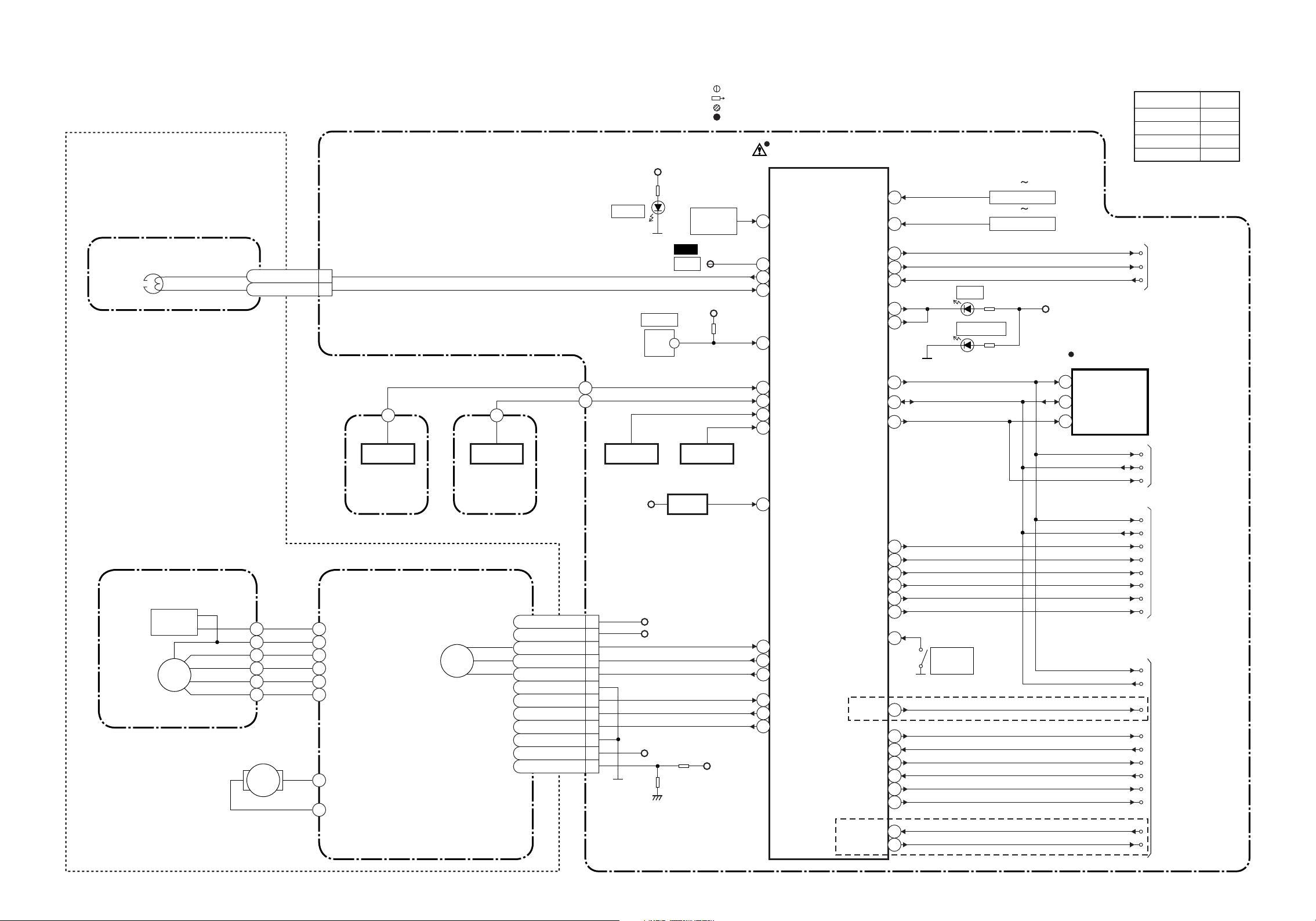
[ 21PV375/ ( 01, 07, 39, 58 ) ]
Servo/System Control Block Diagram
(DECK ASSEMBLY)
MAIN CBA
BLOCK DIAGRAMS
NOTE FOR WIRE CONNECTORS:
1. PREFIX SYMBOL "CN" MEANS CONNECTOR.
(CAN DISCONNECT AND RECONNECT.)
2. PREFIX SYMBOL "CL" MEANS WIRE-SOLDER
HOLES OF THE PCB.
(WIRE IS SOLDERED DIRECTLY.)
D201
S-LED
AL+5V
TEST POINT INFORMATION
RS201
:INDICATES A TEST POINT WITH A JUMPER WIRE ACROSS A HOLE IN THE PCB.
:USED TO INDICATE A TEST POINT WITH A COMPONENT LEAD ON FOIL SIDE.
:USED TO INDICATE A TEST POINT WITH NO TEST PIN.
:USED TO INDICATE A TEST POINT WITH A TEST PIN.
IC201
(SERVO/SYSTEM CONTROL)
REMOTE
SENSOR
REMOTE
14
KEY-1
KEY-2
Comparison Chart of
Models & Marks
Model Mark
21PV375/07
21PV375/01
21PV375/58
21PV375/39
SW201 SW205
7
8
KEY SWITCH
SW206 SW210
KEY SWITCH
I
J
K
L
AC HEAD ASSEMBLY
CONTROL
HEAD
CYLINDER ASSEMBLY
PG
SENSOR
DRUM
MOTOR
M
LOADING
MOTOR
M
CL402
2CTL(+)
1CTL(-)
SENSOR CBA
(ST-SENSOR)
Q202 Q205Q201
ST-SENS.
END-SENS.
SENSOR CBA
(END-SENSOR)
CAPSTAN MOTOR
CAPSTAN
MOTOR
M
C-CONT
D-PFG
TIMER+5V
CN201
1CM+12V/20.5V
2P-ON+5V(3)
3C-FG
4C-F/R
5
6FG-GND
7LD-CONT
8D-CONT
9
10M-GND
11AL+12V(1)
12VG
T-REEL
WF3
CTL
SW212
LD-SW
PI201
S-REEL
Q204
RESET
CM+12V/20.5V
P-ON+5V(3)
AL+12V(1)
TP001
AL+5V
+33V
CTL AMP-OUT
97
95
CTL(+)
CTL(-)
94
LD-SW9
10
ST-SENS.
4
END-SENS.
T-REEL
80
S-REEL
79
34
RESET
C-FG
87
C-F/R
78
C-CONT
76
81
LD-CONT
77
D-CONT
90
D-PFG
C-POWER-SW
P-ON-H
P-DOWN-L
REC LED
REC LED
SCL
SDA
I2C-OPEN
SP-MUTE
A-MUTE-H
1ST-SND-H
EXT-L
SCART-H
SCART-MUTE
REC-SAFETY
I, J, K
DAVN-L
D-REC-H
C-SYNC
DV-SYNC
V-ENV
C-ROTA
RF-SW
L
TRICK-H
SECAM-H
66
67
85
23
24
71
72
45
44
20
21
42
48
29
31
83
47
74
13
15
18
33
32
C-POWER-SW
P-ON-H
P-DOWN-L
D202 REC
AL+5V
D204 STANDBY
(MEMORY)
IC202
SCL
6
5
SDA
CS
7
SCL
SDA
I2C-OPEN
SCL
SDA
SP-MUTE
A-MUTE-H
1ST-SND-H
EXT-L
SCART-H
SCART-MUTE
SW211
REC
SAFETY
6
SCL
SDA
DAVN-L
D-REC-H
C-SYNC
DV-SYNC
V-ENV
C-ROTA
RF-SW
TRICK-H
SECAM-H
FROM/TO POWER
SUPPLY BLOCK
FROM/TO CHROMA
BLOCK
FROM/TO AUDIO
BLOCK
FROM/TO VIDEO
BLOCK
1-7-15 1-7-16 T6500BLS
Video Block Diagram
" " = SMD
MAIN CBA
TO CHROMA BLOCK
TU001
VIDEO OUT
TU002
VIDEO OUT
JK701
V-IN
JK703
V-IN
20
V-OUT
TO CHROMA
BLOCK
19
NOTE FOR WIRE CONNECTORS:
1. PREFIX SYMBOL "CN" MEANS CONNECTOR.
(CAN DISCONNECT AND RECONNECT.)
2. PREFIX SYMBOL "CL" MEANS WIRE-SOLDER
HOLES OF THE PCB.
(WIRE IS SOLDERED DIRECTLY.)
24
24
BUFFER
Q703
TU1-VIDEO
VIDEO
Q705
C-VIDEO
BUFFER
TP003
V-OUT
WF5
Q401
BUFFER
IC401
(VIDEO/AUDIO SIGNAL PROCESS)
WF4
48
50
52
54
56
61
63
TUNER1
TUNER2
SCART
LINE
SCART
LINE
PB/EE
MUTE
TUNER1
TUNER2
PB/EE
MUTE
TEST POINT INFORMATION
:INDICATES A TEST POINT WITH A JUMPER WIRE ACROSS A HOLE IN THE PCB.
:USED TO INDICATE A TEST POINT WITH A COMPONENT LEAD ON FOIL SIDE.
:USED TO INDICATE A TEST POINT WITH NO TEST PIN.
:USED TO INDICATE A TEST POINT WITH A TEST PIN.
FROM /TO
SERVO/SYSTEM
CONTROL BLOCK
65
BYPASS
AGC
CHARA.
INS.
FBC
AGC VXO
58 59
PR
Y. DELAY
1/2
DAVN-L
SDA
SCL
LUMINANCE
SIGNAL
PROCESS
Y/C
MIX
REC-VIDEO SIGNAL PB-VIDEO SIGNAL MODE: SP/REC
69684643
7978
SERIAL
DECORDER
R
P
CCD 1H DELAY
Y
+
C
CHROMINANCE
SIGNAL
PROCESS
R P R P
2928 44
21
14
6
7
16
REC FM
AGC
PB-H OUT
IC101 (VPS)
DAVN-L
SDA
SCL
VPS-V
SP
HEAD
AMP
D-REC-H
RF-SW/C-ROTA
D-V-SYNC
C-SYNC
V-ENV
I, J, K
96
95
93
94
80
70
62
84
67
WF1
TP002
RF-SW
Comparison Chart of
Models & Marks
21PV375/07
21PV375/01
21PV375/58
21PV375/39
(DECK ASSEMBLY)
CL401
V(R)
1
V-COM
V(L)
2
3
D-REC-H
RF-SW
C-ROTA
D-V-SYNC
V-ENV
C-SYNC
TRICK-H
SECAM-H
IC471 (PAL/SECAM DECTECOTR)
CYLINDER ASSEMBLY
FROM/TO SERVO/SYSTEM
CONTROL BLOCK
Model Mark
I
J
K
L
VIDEO (R)
HEAD
VIDEO (L)
HEAD
L
28
29
17
12
16
14
1
PAL/SECAM
2
DETECTOR
TP010
GND
X401
4.43MHz
WF2
TP008
C-PB
WF6
1-7-17 1-7-18 T6500BLV

Audio Block Diagram
NOTE FOR WIRE CONNECTORS:
1. PREFIX SYMBOL "CN" MEANS CONNECTOR.
(CAN DISCONNECT AND RECONNECT.)
" " = SMD
2. PREFIX SYMBOL "CL" MEANS WIRE-SOLDER
HOLES OF THE PCB.
(WIRE IS SOLDERED DIRECTLY.)
TEST POINT INFORMATION
:INDICATES A TEST POINT WITH A JUMPER WIRE ACROSS A HOLE IN THE PCB.
:USED TO INDICATE A TEST POINT WITH A COMPONENT LEAD ON FOIL SIDE.
:USED TO INDICATE A TEST POINT WITH NO TEST PIN.
:USED TO INDICATE A TEST POINT WITH A TEST PIN.
PB-AUDIO SIGNAL REC-AUDIO SIGNAL Mode : SP/REC
TU001
AUDIO OUT
AUDIO OUT
TU002
JK702
A-IN
A-IN
A-OUT
21
21
JK703
2
1
Q701
(DECK ASSEMBLY)
IC702 (SW)
14
SW CTL
11
TU1
TU2
13
12
13
12
IC701 (SW)
1
2
5
3
SW CTL
1011 9
1ST-SND-H
SCART-MUTE
15
4
14
SCART-H
EXT-L
FROM SERVO
/SYSTEM
CONTROL
BLOCK
WF7
52
53
54
(VIDEO/AUDIO/CHROMA/DEFLECTION/IF)
IC301
TUNER1
LINE
AUDIO
MUTE
+5V
Q854
ATT
50
IC401
(AUDIO SIGNAL PROCESS)
TUNER1
13
TUNER2
15
LINE
17
PB-ON
5
6
EQ
AMP
SP/LP-ON
MAIN CBA
IC151 (AMP)
7
WF9
7
OUTPUT
AMP
MUTE
5
98
1
SP-MUTE
(FROM PIN 44 OF IC201)
INV
ATT
CN151
SP
SP-GND 2
R
P
ALC
DET
ALC
1
CL801
LINE
AMP
REC-ON
JK151
HEADPHONE JACK
SP151
SPEAKER
12
MUTE
11
TP007
A-OUT
WF8
AUDIO
HEAD
AUDIO
ERASE
HEAD
ACE HEAD ASSEMBLY
FULL
ERASE
HEAD
FE HEAD
CL402
3 A-PB/REC
4 A-COM
6 AE-H
5 FE-H
CL403
1 FE-H
2 FE-H-GND
Q855
BIAS
OSC
Q856
Q853(PB=ON)
Q851
Q852(PB=ON)
SWITCHING
D-REC-OFF
1
2
+5V
AUTO
BIAS
3
100
REC
AMP
SERIAL
AUDIO HD-SW
DECODER
CONTROL
16
68 69
71
A-MUTE-H
SDA
SCL
FROM/TO
SERVO/SYSTEM
CONTROL BLOCK
1-7-19 1-7-20 T6500BLA
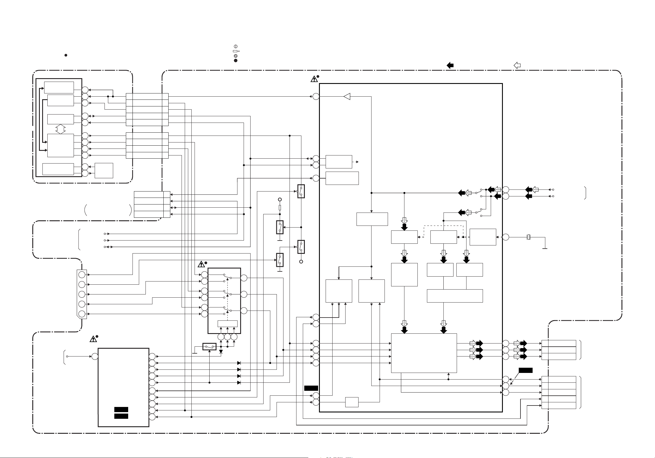
Chroma Block Diagram
NOTE FOR WIRE CONNECTORS:
1. PREFIX SYMBOL "CN" MEANS CONNECTOR.
(CAN DISCONNECT AND RECONNECT.)
" " = SMD
IC901 (TELETEXT DECODER)
ADC/
DATA SLICER
DISPLAY
TIMING
I2C I/F
TELETEXT
DECODER
OSC/CLOCK
GENERATOR
23
37
36
50
49
35
32
33
34
41
42
TEXT CBA
CN303 is used for
adjustment at factory
FROM/TO
SERVO/SYSTEM
CONTROL BLOCK
I2C-OPEN
2. PREFIX SYMBOL "CL" MEANS WIRE-SOLDER
HOLES OF THE PCB.
(WIRE IS SOLDERED DIRECTLY.)
X901
12MHz
OSC
SCL
SDA
CN901 CN751
5 5Y-SW-OUT
1 1V-SYNC
2 2H-SYNC
4 4SDA
3 3SCL
CN752CN902
2 2OSD-BLK
4 4OSD-B
6 6OSD-G
3 3OSD-R
(NO CONNECTION)
INT.MONITOR
I2C-OPEN 2
SDA 4
SCL 5
CN303
1
TEST POINT INFORMATION
:INDICATES A TEST POINT WITH A JUMPER WIRE ACROSS A HOLE IN THE PCB.
:USED TO INDICATE A TEST POINT WITH A COMPONENT LEAD ON FOIL SIDE.
:USED TO INDICATE A TEST POINT WITH NO TEST PIN.
:USED TO INDICATE A TEST POINT WITH A TEST PIN.
Q706
Q702
+5V
Q711
Q704
IC301
40
10
11
43
(VIDEO/AUDIO/CHROMA/DEFLECTION/IF)
SERIAL
I/F
INTELLIGENT
MONITORING
SYNC
SEPARATION
CHROMA
TRAP
CHROMA
BPF
REC VIDEO SIGNAL PB VIDEO SIGNAL
MAIN CBA
LINE/PB
TUNER
LINE/PB
TUNER
CLOCK
CONTROL
CIRCUIT
34
36
32
VIDEO
TU1-VIDEO
X301
4.43MHz
Mode : SP/REC
FROM
VIDEO BLOCK
SLOW-SW
RAPID-SW
FROM
VIDEO
BLOCK
OSD-B
OSD-G
OSD-R
C-VIDEO
8
16
7
11
15
JK703
IC201
(SYSTEM CONTROL/OSD)
C-VIDEO
56
SLOW-SW-IN
RAPID-SW-IN
WF18
WF17
TEXT-L
OSD-R
OSD-G
OSD-B
OSD-BLK
RGB CONT
V-SYNC
H-SYNC
82
64
63
62
60
68
61
65
59
58
IC703 (SW)
5
3
2
1
12
13
Q710
SW CTL
109 11
15
14
+5V
LUMA
SIGNAL
4
V-SYNC
PROCESS
CIRCUIT
H-SYNC
PROCESS
CIRCUIT
PROCESS
CIRCUIT
PAL
DECODER
BASE BAND
SECAM
DECODER
1H DELAY LINE
17
21
CL301A
27
20
28
OSD MIX/RBG MATRIX/
BLANKING
16
15
14
BLUE2
GREEN1
RED
3
TO
CRT/H.V. BLOCK
CL301B
30
WF10
13
12
WF11
6
7
31
INV
CL302A
FBP3
H-DRIVE2
ACL6
V-RAMP-FB5
V-DRIVE4
FROM/TO
CRT/H.V. BLOCK
CL302B
T6500BLC1-7-21 1-7-22

CRT/H.V. Block Diagram
NOTE FOR WIRE CONNECTORS:
1. PREFIX SYMBOL "CN" MEANS CONNECTOR.
(CAN DISCONNECT AND RECONNECT.)
" " = SMD
2. PREFIX SYMBOL "CL" MEANS WIRE-SOLDER
HOLES OF THE PCB.
(WIRE IS SOLDERED DIRECTLY.)
TEST POINT INFORMATION
:INDICATES A TEST POINT WITH A JUMPER WIRE ACROSS A HOLE IN THE PCB.
:USED TO INDICATE A TEST POINT WITH A COMPONENT LEAD ON FOIL SIDE.
:USED TO INDICATE A TEST POINT WITH NO TEST PIN.
:USED TO INDICATE A TEST POINT WITH A TEST PIN.
REC VIDEO SIGNAL PB VIDEO SIGNAL
Mode : SP/REC
FROM
POWER SUPPLY BLOCK
JUNCTION-B
CBA
3
FROM/TO
CHROMA BLOCK
CL302A
3
6
5
4
H.V./POWER SUPPLY CBA
+B
DEF+B
CN302CL302B
3 3FBP
2 2H-DRIVE
6 6ACL
5 5V-RAMP-FB
4 4V-DRIVE
CN552
Q533
H.DRIVE
WF12
Q551
H.OUTPUT
T552
1
5
3
4
T551 F.B.T.
10
IC551 (V-DEFLECTION CONTROL)
THERMAL
7
AMP
1
6
FOCUS VR
HV
F
S
11
8
7
9
6
SCREEN VR
PROTECTION
PUMP
UP
VCC
2
3
ANODE
FOCUS
SCREEN
HEATER 11
P-ON+160V 33
5
CL501BCL501A
WF13
CN551
L551
DEFLECTION-YOKE
5
4
3
1
VDRIVE
HDRIVE
ANODE
FROM CHROMA
BLOCK CL301A
CN301CL301B
2
4
3
JUNCTION-C
CBA
2 2RED
4 4GREEN
3 3BLUE
CN502
Q501
RED AMP
CRT CBA
Q502
GREEN AMP
JK501
FOCUS
WF15WF14
BLUE AMP
Q503
WF16
CN501
1-7-241-7-23
SCREEN
GND
R
G
B
HEATER
GND
T6500BLCRT
V501
CRT
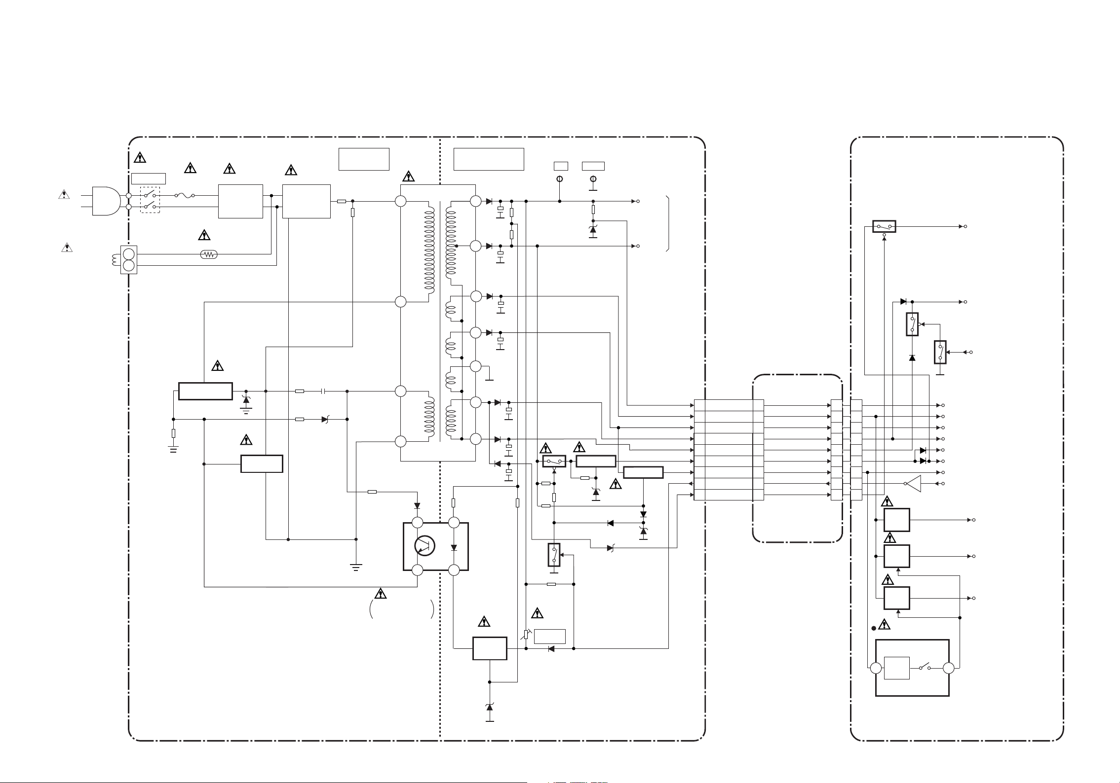
Power Supply Block Diagram
W601
DG601
DEGAUSSING
COIL
CAUTION !
Fixed voltage power supply circuit is used in this unit.
If Main Fuse (F601) is blown, check to see that all components in the power supply
circuit are not defective before you connect the AC plug to the AC power supply.
Otherwise it may cause some components in the power supply circuit to fail.
SW602
POWER
CN601
F601
T4A/250V
PS602
Q602
SWITCHING
L601,L602
LINE
FILTER
Q603
LIMITER
D601 - D604
BRIDGE
RECTIFIER
HOT COLD
T601
6
4
2
1
4 1
3 2
IC601
ERROR
VOLTAGE DET
14
13
12
11
10
9
8
Q604
FEED
BACK
CAUTION
FOR CONTINUED PROTECTION AGAINST FIRE HAZARD,
REPLACE ONLY WITH THE SAME TYPE T4A/250V FUSE.
TP503
Q608
VR601
+B ADJ.
+B
TP504
GND
Q606Q605
+5V REG.
+B
DEF+B
+8V REG.
Q607
TO
CRT/H.V.
BLOCK
CN602
5
12
6
4
AL+33V11
AL+9V8
AL+12V(2)7
AL+12V(1)3
AL+20.5V2
AL+5V
P-ON+8V
P-ON-L
P-DOWN-L
NOTE :
The voltage for parts in hot circuit is measured using
hot GND as a common terminal.
CL603BCN603
11
8
7
3
2
5
12
6
4
JUNCTION-A CBA
11
12
8
7
3
2
5
6
4
CL603A
11
8
7
3
2
5
12
6
4
Q206
IC301
Q682
IC681
+5V
REG.
Q684
+5V
REG.
Q686
+5V
REG.
+5.7V
REG.
P-DOWN-L
(TO PIN85 OF IC201)
CM+12V/20.5V
Q681
Q683
C-POWER-SW
(FROM PIN66 OF IC201)
AL+33V
AL+9V
AL+12V(2)
AL+12V(1)
TIMER+5V
AL+5V
P-ON+8V
P-ON-H
(FROM PIN67 OF IC201)
P-ON+5V(2)
P-ON+5V(3)
P-ON+5V(1)
P-ON-ON
3955
1-7-25
H.V./POWER SUPPLY CBA
1-7-26
MAIN CBA
T6500BLP

[ 21PV375/ ( 01, 07, 39, 57 ) ]
Main 1/5 Schematic Diagram Parts Location Guide
Ref No. Position Ref No. Position Ref No. Position Ref No. Position
CAPACITORS
C203
C205
C207
C208
C209
C210
C211
C212
C213
C214
C217
C218
C221
C222
C223
C224
C225
C226
C227
C228
C229
C230
C231
C233
C234
C235
C236
C237
C238
C239
C240
C241
C242
C243
C244
C245 C-4 R216 A-4 R263 A-4 RS201 B-1
C248
C253
C254
C255
C256
CONNECTOR
CN201 F-5 R223 B-2 R270 B-1
B-3
B-3
B-1
B-1
C-1
C-1
B-1
B-1
B-1
B-1
C-1
C-1
D-2
D-2
D-2
D-2
D-2
D-2
D-3
D-3 RESISTORS
D-3
E-3
D-4
D-4
D-4
C-4
C-4
C-4
C-4
C-4
C-4
C-4
D-4
D-4
C-4
B-1
B-2
C-4
C-4
C-1
D201
D202
D204
D205
D206
D210
D211
D212
D213
D214
IC201
IC202
L201
TRANSISTORS
Q204
Q205
Q206
R201
R202
R203
R204
R205
R206
R207
R208
R209
R210
R211
R212
R213
R214
R215
R217
R218
R219
R220
R221
R222
DIODES
ICS
COIL
B-3
B-2
B-2
B-1
D-3
D-2
D-2
D-2
A-4
A-4
C-3
D-1
D-2
B-1
D-4
C-4
B-4
B-4
B-3
B-4
B-3
B-3
B-4
B-4
A-4
A-4
A-4
A-4
B-4
B-4
A-4
A-4
B-3
B-3
B-3
B-3
B-3
RESISTORS RESISTORS
R224
R226
R227
R228
R229
R230
R231
R232
R233
R234
R235
R236
R237
R238
R239
R240
R241
R242
R243
R244
R248
R249
R250
R251
R252
R253
R254
R255
R256
R257
R258
R259
R260
R261
R262
R264
R265
R266
R267
R268
R269
B-2
B-1
B-1
B-1
B-1
B-1
C-1
C-1
C-1
C-1
D-2
D-2
D-2
D-2
D-2
D-2
D-3
D-3
D-3
D-3
D-3
D-3
D-3
D-4
D-4
D-3
C-4
C-4
C-4
B-3
B-4
B-4
A-4
A-4
A-4
A-4
D-1
D-1
E-1
E-3
E-3
R271
R272
R273
R274
R275
R276
R277
R278
R279
R280
R281
R282
R287
R288
R289
SWITCH ES
SW201
SW202
SW203
SW204
SW205
SW206
SW207
SW208
SW209
SW210
SW211
SW212
TEST POINT
TP001
CRYSTAL OSCILATORS
X201
X202
MISCELLANEOUS
PI201
B-2
B-3
B-2
B-2
D-2
D-2
D-2
D-2
D-2
D-2
C-1
D-2
B-1
E-1
E-1
B-4
A-4
A-4
A-4
A-4
B-4
A-4
A-4
A-4
A-4
B-1
A-4
C-4
C-1
C-1
D-4
1-8-43

Main 1/5 Schematic Diagram
Comparison Chart of
MODEL MARK
21PV375/07 I
21PV375/01 J
21PV375/58 K
21PV375/39 L
“ “ = SMD
Voltage indications for PLAY and REC modes on
the Schematic Diagrams are as shown below:
1 2 3
5.0
THE SAME VOLTAGE FOR
BOTH PLAY & REC MODES.
5.0
~
(2.5)
INDICATES THAT THE VOLTAGE
IS NOT CONSISTENT HERE.
PLAY MODE
REC MODE
Models and Marks
1-8-44 1-8-45
T6500SCM1
 Loading...