

Panasonic TY-TP42P10S, TY-TP50P10S Service Manual
ORDER NO. ITD0805032CE
Touch Panel
Model No. TY-TP42P10S
Model No. TY-TP50P10S
TABLE OF CONTENTS
1 Warning-------------------------------------------------------------- 2
1.1. Prevention of Electrostatic Discharge (ESD)
to Electrostatically Sensitive (ES) Devices---------- 2
1.2. About lead free solder (PbF)---------------------------- 3
2 Specifications ----------------------------------------------------- 4
3 General/Introduction -------------------------------------------- 5
3.1. PCB Stracture---------------------------------------------- 5
4 Operating Instructions------------------------------------------6
5 Disassembly and Assembly Instructions ---------------40
5.1. Remove the Frame U Assy ----------------------------40
5.2. Remove the Cover-U Assy-----------------------------40
5.3. Remove the Flat bracing metal -----------------------40
5.4. Remove the Main board unit---------------------------40
5.5. Remove the Sensor-L board unit---------------------40
5.6. Remove the Sensor-R board unit --------------------40
5.7. Remove the Right angle-UL ---------------------------41
5.8. Remove the Right angle-UR------------------- --------41
6 Measurements and Adjustments---------------------------42
PAGE PAGE
6.1. Before the adjustment when Circuit board are
exchanged------------------------------------------------- 42
6.2. Cautions for replacing the Circuit board------------ 42
6.3. Flow chart for replacing the Boards -----------------42
6.4. How to rewrite data when replacing the Main
Board-------------------------------------------------------- 43
6.5. Adjust the optical axis----------------------------------- 43
6.6. Adjust PEAKPOSI (Corner) --------------------------- 45
6.7. Setting range (first, last) of the optical axis--------46
6.8. Adjust and confirm the light level--------------------- 47
7 25-point calibration---------------------------------------------48
7.1. Prepare setting for adjusting PC--------------------- 48
7.2. Explanation of 25-point Calibration------------------48
8Dimensions-------------------------------------------------------51
9 Block Diagram --------------------------------------------------- 52
10 Schematic Diagram --------------------------------------------53
10.1. Main Board Unit Schematic Diagram ---------------53
10.2. Sensor Board Unit Schematic Diagram ------------54
© 2008 Matsushita Electric Industrial Co., Ltd. All
rights reserved. Unauthorized copying and distribution is a violation of law.
TY-TP42P10S / TY-TP50P10S
1Warning
1.1. Prevention of Electrostatic Discharge (ESD) to Electrostatically Sensitive (ES) Devices
Some semiconductor (solid state) devices can be damaged easily by static electricity. Such components commonly are called Electrostatically Sensitive (ES) Devices. Examples of typical ES devices are integrated circuits and some field-effect transistors and
semiconductor "chip" components. The following techniques should be used to help reduce the incidence of component damage
caused by electrostatic discharge (ESD).
1. Immediately before handling any semiconductor component or semiconductor-equipped assembly, drain off any ESD on your
body by touching a known earth ground. Alternatively, obtain and wear a commercially available discharging ESD wrist strap,
which should be removed for potential shock reasons prior to applying power to the unit under test.
2. After removing an electrical assembly equipped with ES devices, place the assembly on a conductive surface such as aluminum foil, to prevent electrostatic charge buildup or exposure of the assembly.
3. Use only a grounded-tip soldering iron to solder or unsolder ES devices.
4. Use only an anti-static solder removal device. Some solder removal devices not classified as "anti-static (ESD protected)"
can generate electrical charge sufficient to damage ES devices.
5. Do not use freon-propelled chemicals. These can generate electrical charges sufficient to damage ES devices.
6. Do not remove a replacement ES device from its protective package until immediately before you are ready to install it. (Most
replacement ES devices are packaged with leads electrically shorted together by conductive foam, aluminum foil or comparable conductive material).
7. Immediately before removing the protective material from the leads of a replacement ES device, touch the protective material
to the chassis or circuit assembly into which the device will be installed.
Caution
Be sure no power is applied to the chassis or circuit, and observe all other safety precautions.
8. Minimize bodily motions when handling unpackaged replacement ES devices. (Otherwise ham less motion such as the brushing together of your clothes fabric or the lifting of your foot from a carpeted floor can generate static electricity (ESD) sufficient
to damage an ES device).
2
TY-TP42P10S / TY-TP50P10S
1.2. About lead free solder (PbF)
Note: Lead is listed as (Pb) in the periodic table of elements.
In the information below, Pb will refer to Lead solder, and PbF will refer to Lead Free Solder.
The Lead Free Solder used in our manufacturing process and discussed below is (Sn+Ag+Cu).
That is Tin (Sn), Silver (Ag) and Copper (Cu) although other types are available.
This model uses Pb Free solder in it’s manufacture due to environmental conservation issues. For service and repair work, we’d
suggest the use of Pb free solder as well, although Pb solder may be used.
PCBs manufactured using lead free solder will have the PbF within a leaf Symbol PbF stamped on the back of PCB.
Caution
• Pb free solder has a higher melting point than standard solder. Typically the melting point is 50 ~ 70 °F (30~40 °C) higher. Please
use a high temperature soldering iron and set it to 700 ± 20 °F (370 ± 10 °C).
• Pb free solder will tend to splash when heated too high (about 1100 °F or 600 °C).
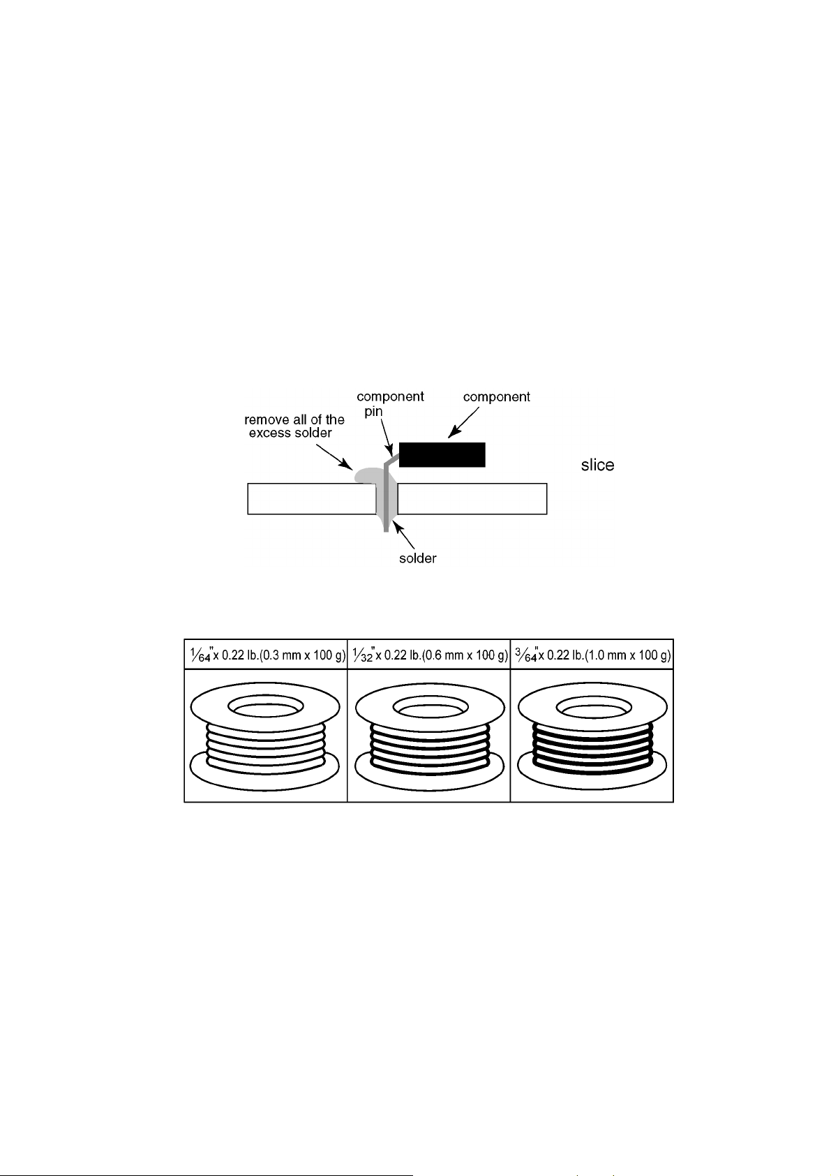
If you must use Pb solder, please completely remove all of the Pb free solder on the pins or solder area before applying Pb solder. If this is not practical, be sure to heat the Pb free solder until it melts, before applying Pb solder.
• After applying PbF solder to double layered boards, please check the component side for excess solder which may flow onto the
opposite side. (see figure below)
Suggested Pb free solder
There are several kinds of Pb free solder available for purchase. This product uses Sn+Ag+Cu (tin, silver, copper) solder. However, Sn+Cu (tin, copper), Sn+Zn+Bi (tin, zinc, bismuth) solder can also be used.
3

TY-TP42P10S / TY-TP50P10S
2 Specifications
Typ e Touch Panel
Power source
Vol tag e +5V DC ± 10%
Electric current Max. 450 mA
Supply system From USB bus
Touch panel
Detection system Infrared retroreflective detection
Panel window
Detection range
Effective detection range Same as above
Resolution Approx. 32,000 × 18,000 points *1
Output system Coordinate output
Optic element pitch Infrared LED x 4, CMOS image sensor × 2
Minimum detection size
Response rate 100 points / sec
Interface
Temperature When operating: 0 ~ 70°C (0 ~ 40°C) *2
Humidity When operating: 20 ~ 80% (No dewing) *2
Resistance to external Lateral light 2,000 lx + 20% (20° angle of incidence)
light Frontal light 10,000 lx + 20% (90° angle of incidence)
External dimensions
Mass Approx. 9.04 lb. (4.1 kg) (TY-TP42P10S) Approx. 10.14 lb. (4.6 kg) (TY-TP50P10S)
Escutcheon material Aluminum
15
36
/16” (938 mm) (W) × 215/64” (535 mm) (H)
(TY-TP42P10S)
15
36
/
“ (920 mm) (W) × 2013/32” (518 mm) (H)
64
(TY-TP42P10S)
9
/32” (7 mm) (TY-TP42P10S)
USB 2.0 full speed device
Signals: +DATA, -DATA, VCC, GND
Connector: Type B
1
40
/32” (1,016.4 mm) (W) × 27” (686 mm) (H)
57
/64” (47.9 mm) (D) (TY-TP42P10S)
× 1
4427/64” (1,128 mm) (W) × 2533/64” (648 mm) (H)
(TY-TP50P10S)
4335/
“ (1,106 mm) (W) × 241/2” (622 mm) (H)
64
(TY-TP50P10S)
21
/64” (8 mm) (TY-TP50P10S)
1
/2” (1,206.4 mm) (W) × 3129/64” (798.6 mm) (H)
47
57
× 1
/64” (47.9 mm) (D) (TY-TP50P10S)
*1 Resolution obtained by using a dedicated Driver software
*2 When the panel is attached to a Plasma display produced by Matsushita Electric Industrial Co., Ltd.
4
3 General/Introduction
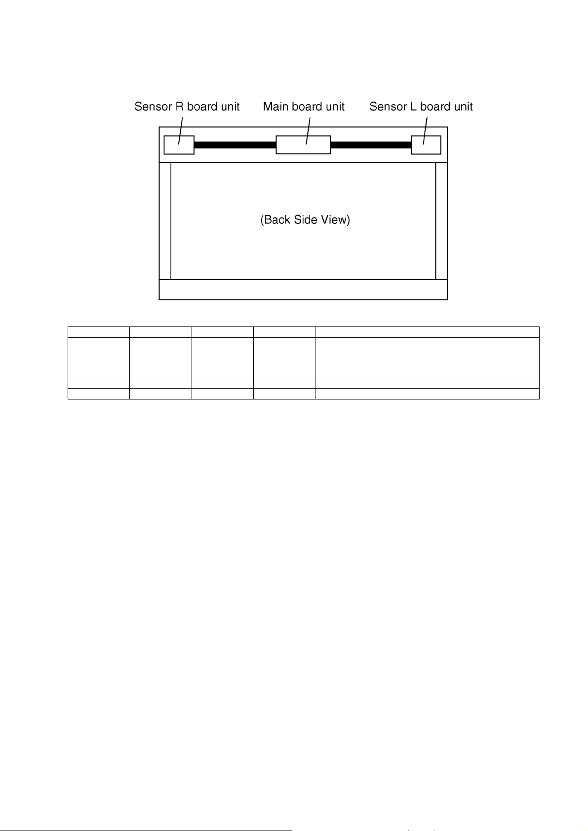
3.1. PCB Stracture
TY-TP42P10S / TY-TP50P10S
Unit Name Board Number Function Contained data Accompanying tasks
Main TXN/12WETB
(TY-TP42P10S)
TXN/11WETB
(TY-TP50P10S)
Sensor-L TXN/22WETB IR sensor L - Adjusting the optical axis. ranee and gain
Sensor-R TXN/31WETB IR sensor R - Adjusting the optical axis, ranee and gain
R-sensor Board and L-sensor Board emit and receive the infrared rays.
Each Board has the infrared LED and image sensor.
Control Board contains data including infrared rays signal. image sensor-receiving position, image sensor sensitivity and its range,
etc in eeprom.
Light receiving-data of left and right sensors is analyzed by this Board and the position is determined.
Main control Adjusted data Copying data, adjusting gain
(If copying is not available, all adjustment is necessary)
5
TY-TP42P10S / TY-TP50P10S
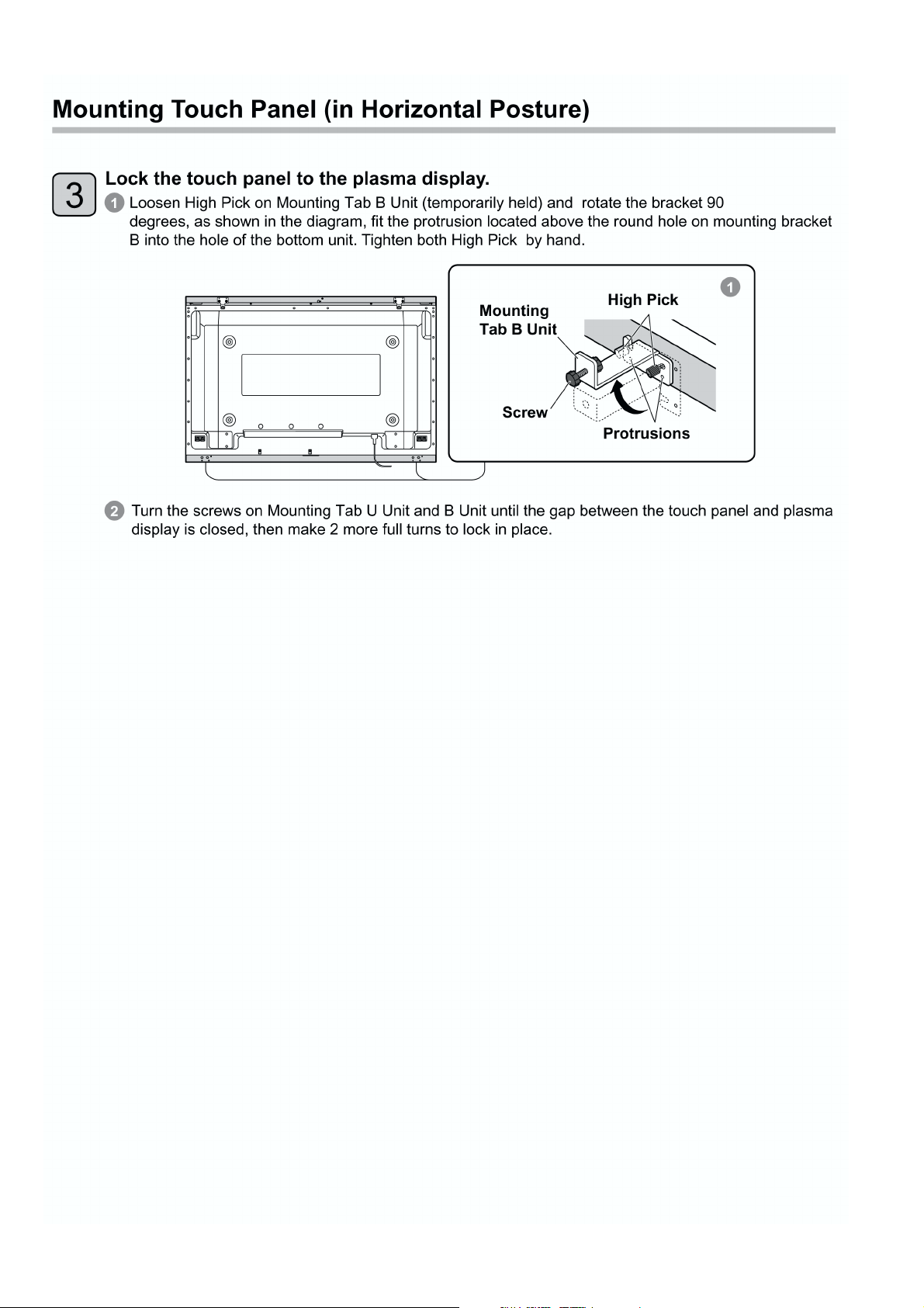
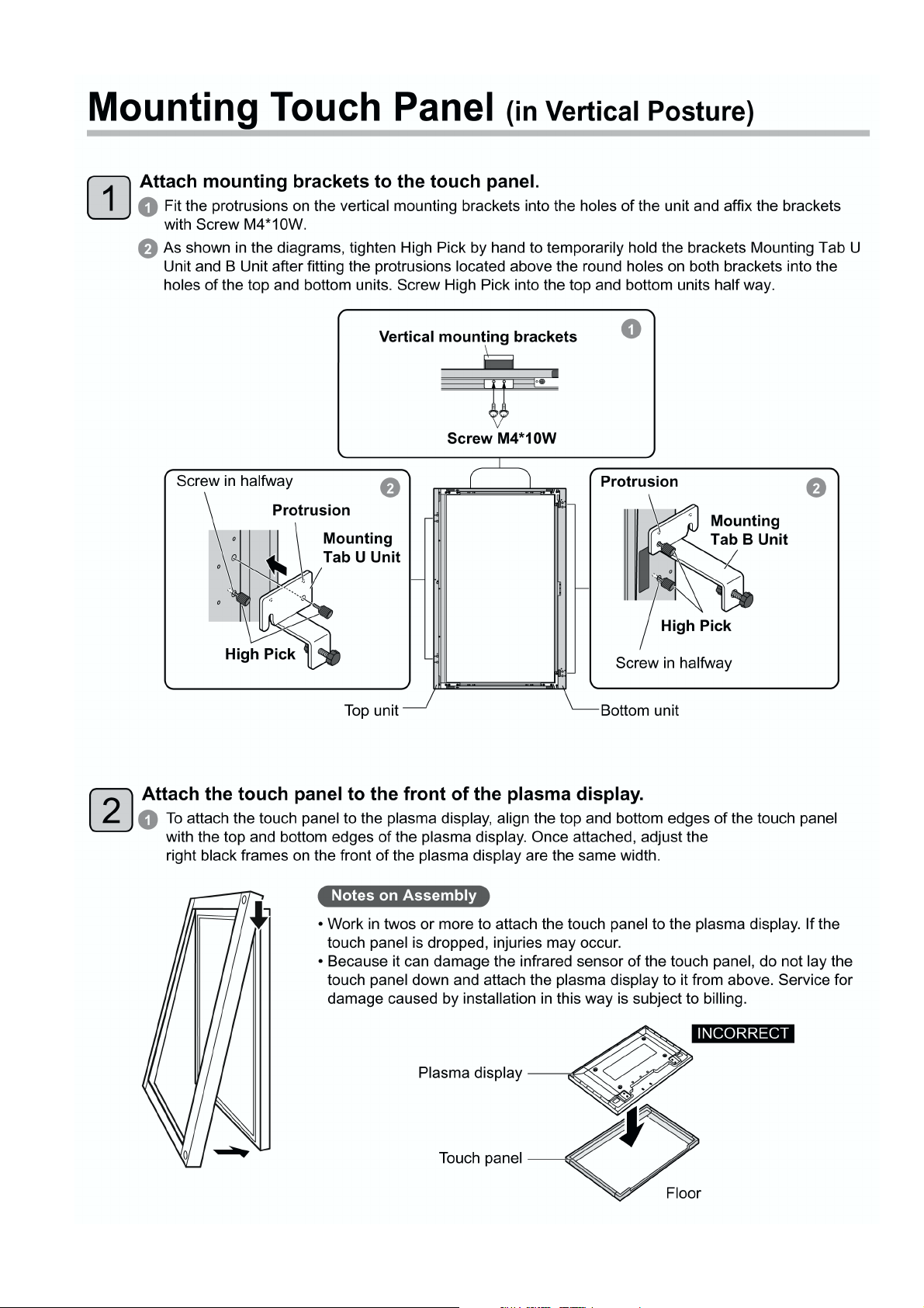
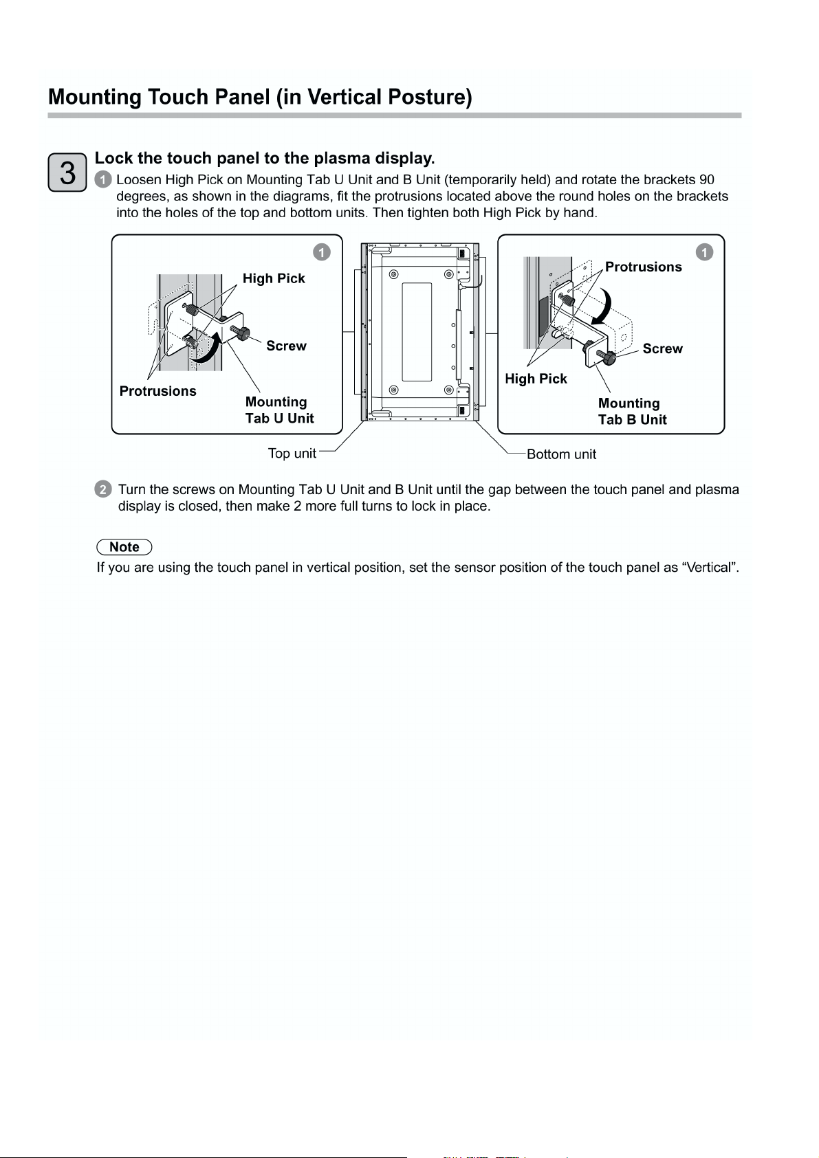
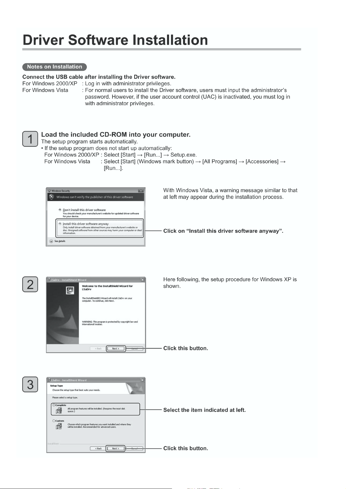
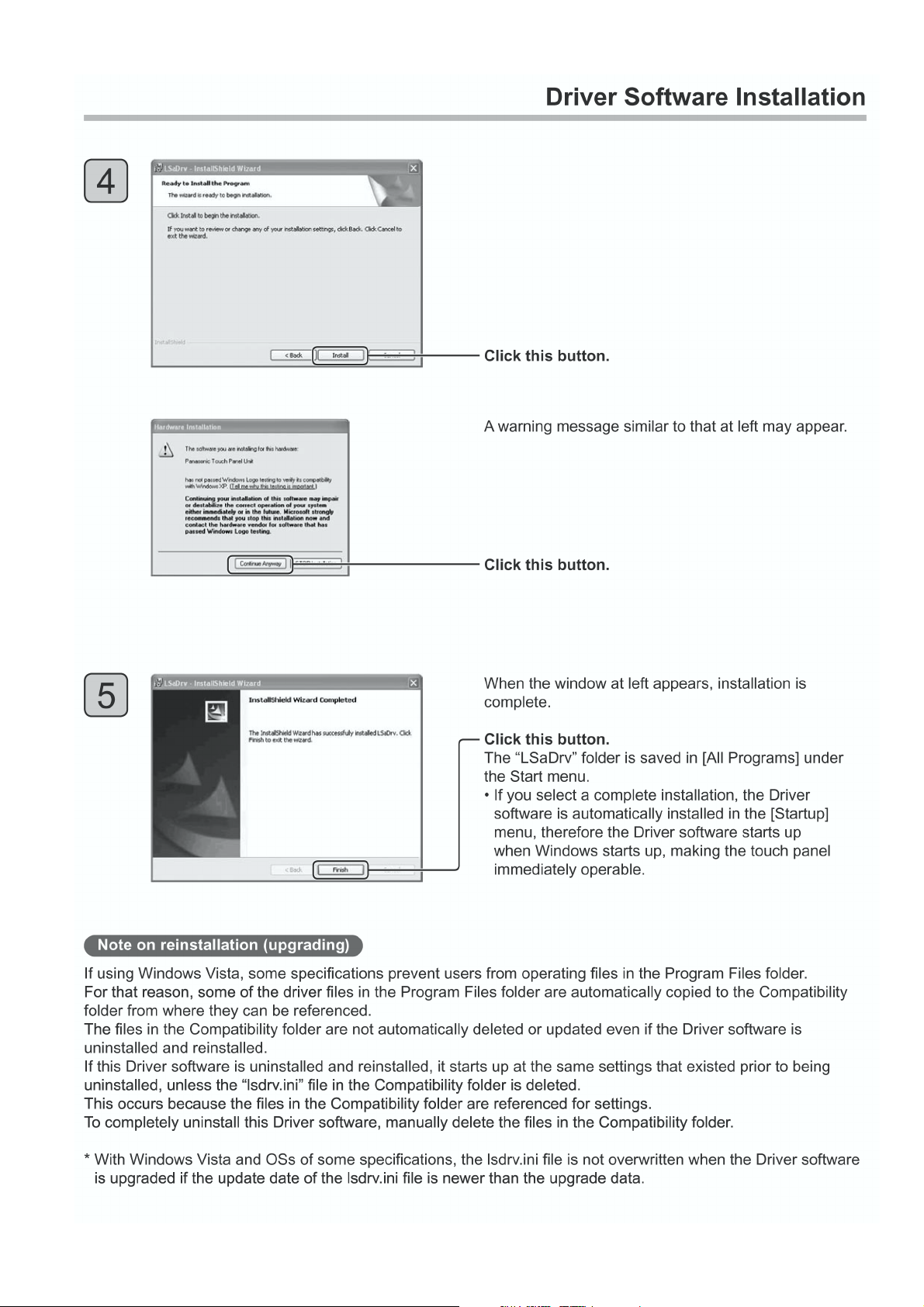
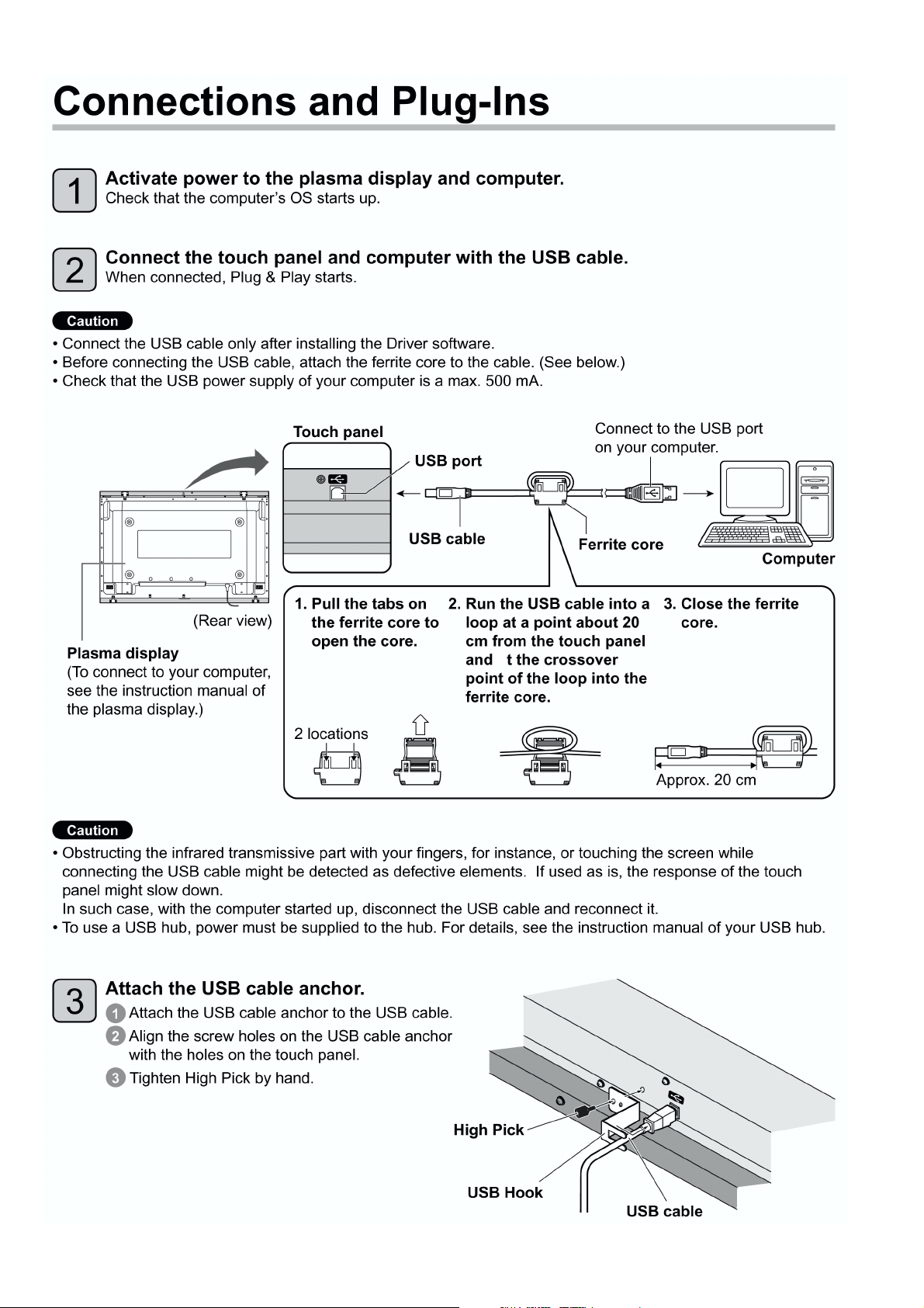
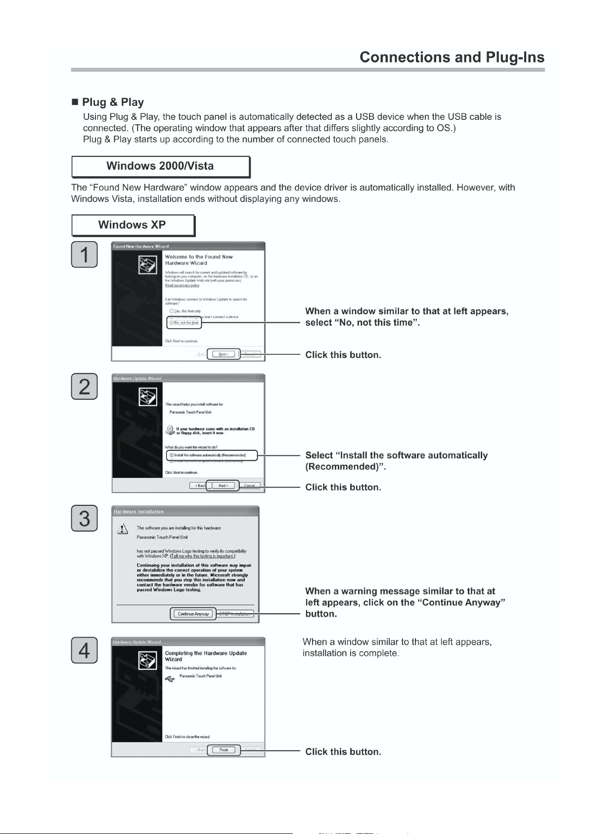
4 Operating Instructions
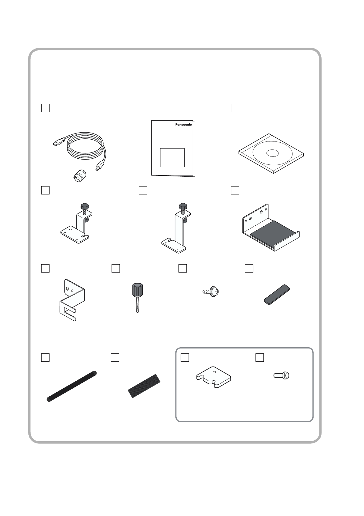
Accessories
Before assembling, attaching and connecting anything, check all accessories have been included in the
product package. Quantities are indicated in ( ).
USB cable (1)
Ferrite core (1)
Mounting Tab U Unit (2)
USB Hook (1) High Pick (9) Screw M4*10 (12)
Instruction Book (7)
• English
• German
• French
• Italian
• Spanish
• Russian
• Ukrainian
Mounting Tab B Unit (2) Vertical Hook Unit (2)
CD-ROM (1)
Driver software
Rubber Pad-S2 (6)*
When you use anti glare*
(options), affix these rubber feet to
the top of the existing rubber feet at
the bottom of the right and left units.
Touch pen (1) Velcro Strip (2) Attached Plate (2) Screw (4)
To use the plasma display with the below pedestal
models, install the spacer included with the touch
panel on the pole of the pedestal as shown.
Applicable pedestals: [TY-ST08-K] [TY-ST08-S]
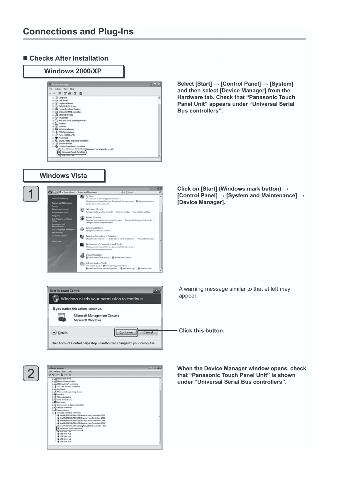
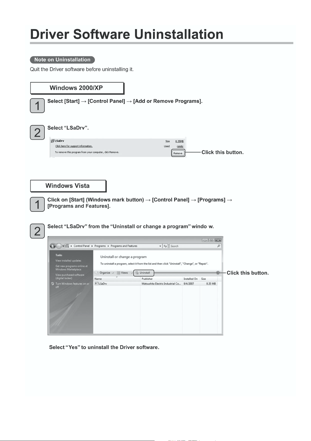
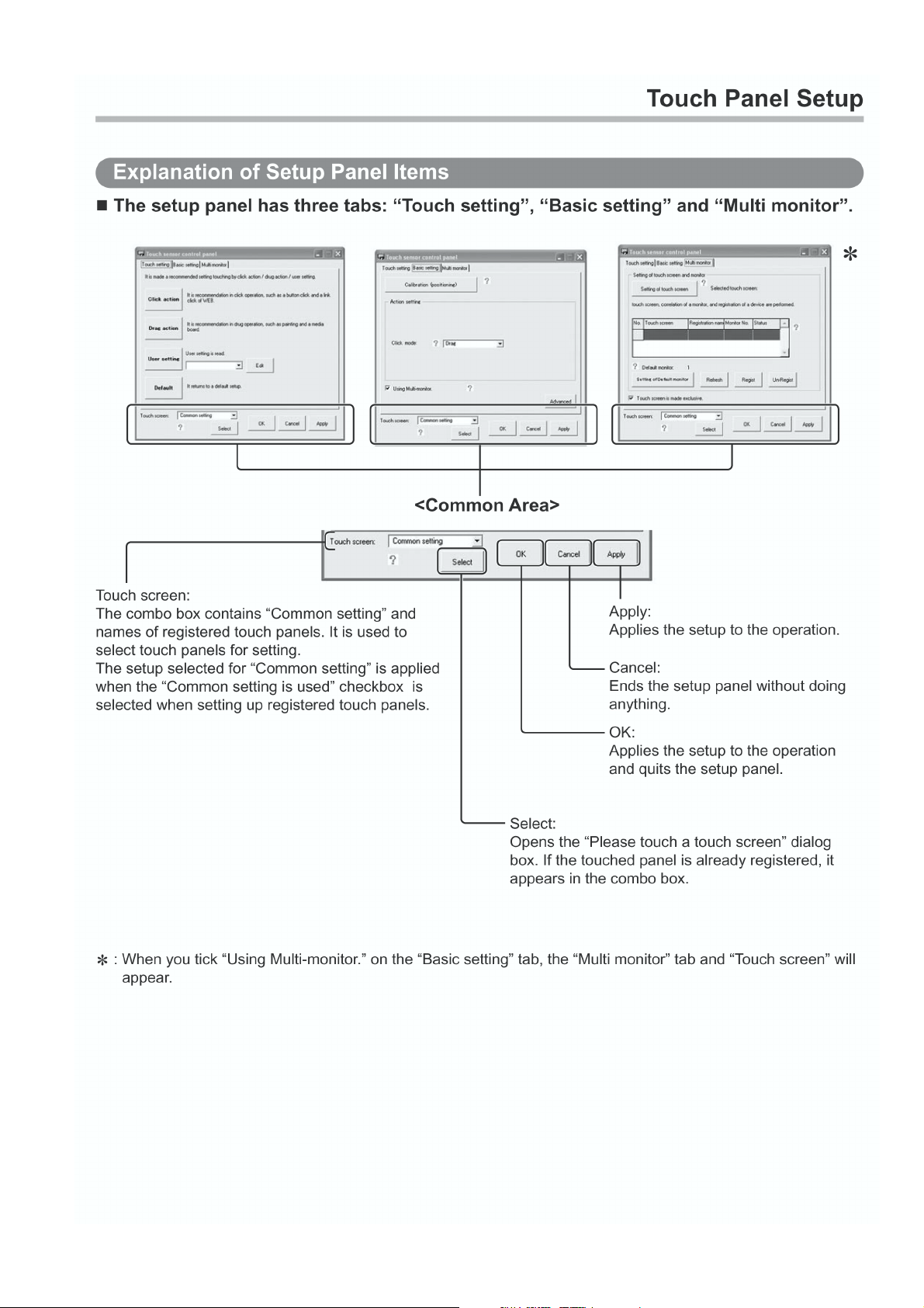
• Illustrations and screens appearing in these operating instructions are conceptual views and may differ
from the actual equipment.
• Windows is a registered trademark of Microsoft Corporation in the USA and other countries. (The official name of
Windows is Microsoft
• The names of other companies and products appearing in this publication are the trademarks, registered
trademarks or products names of their respective owners.
®
Windows®Operating System.)
filters
6
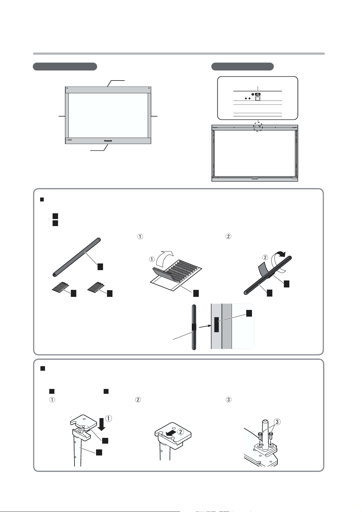
Names of Parts
TY-TP42P10S / TY-TP50P10S
Touch P anel (Fro nt)
Top unit
Left unit
Bottom unit
Attaching the Velcro strip to the touch pen
•
Touch pen
A
Velcro strip (Loop)
B
(with white backing)
the Velcro strip.
Right unit
seirosseccadedulcniwolebehteraperP
Touch Panel (Rear)
morfgnikcabehtffoleeP
the center of the touch pen.
USB port
dnuorapirtsorcleVehtparW
A
B
BB
ne
•
Attach the Velcro strip to the touch panel
so as to hold the touch pen.
PhcuoT
C
C
Touch pen
A
p (Hook)irtsorcleV
(with yellow backing)
Note on attaching the included spacer to the pedestal
To use the plasma display with the below pedestal models, install the spacer included with the touch
panel on the pole of the pedestal as shown. Applicable pedestals: [TY-ST08-K] [TY-ST08-S]
A
Attached Plate
Set the attached plate
over the pole.
B
Pole
Slide the attached plate
in the direction of the arrow.
A
Lock the attached plate to the
pole using the included screws
(25 mm in length).
B
7
TY-TP42P10S / TY-TP50P10S
8
TY-TP42P10S / TY-TP50P10S
9
TY-TP42P10S / TY-TP50P10S
10
TY-TP42P10S / TY-TP50P10S
11
TY-TP42P10S / TY-TP50P10S
12
TY-TP42P10S / TY-TP50P10S
13
TY-TP42P10S / TY-TP50P10S
14
TY-TP42P10S / TY-TP50P10S
15
TY-TP42P10S / TY-TP50P10S
16
TY-TP42P10S / TY-TP50P10S
17
TY-TP42P10S / TY-TP50P10S
18
TY-TP42P10S / TY-TP50P10S
19

TY-TP42P10S / TY-TP50P10S
20
TY-TP42P10S / TY-TP50P10S
21
 Loading...