

Page 1
ORDER NO. MD0703013CE
CD Stereo System
SC-EN35P
SC-EN35PC
Colour
(K)... Black Type
System
SC-EN35P-K
Main Unit: SA-EN35P-K
Speakers: SB-EN35AP-K (L) & SB-EN35P-K (R)
SC-EN35PC-K
Main Unit: SA-EN35PC-K
Speakers: SB-EN35APC-K (L) & SB-EN35PC-K (R)
A6
Specifications
n AMPLIFIER SECTION
FTC OUTPUT POWER both channel driven simultaneously
10% total harmonic distortion (THD)
1 kHz 2.8 W per channel
RMS OUTPUT POWER both channel driven simultaneously
10% total harmonic distortion (THD)
1 kHz 3 W per channel
Output impedance
HEADPHONE 16 Ω to 32 Ω
MUSIC PORT
Phone Jack
Terminal 3.5 mm stereo
Music Port Jack
Terminal 3.5 mm stereo
n TUNER SECTION
Frequency range
FM 87.9 MHz to 107.9 MHz (200 kHz)
87.5 MHz to 108.0 MHz (100 kHz)
AM 520 kHz to 1710 kHz (10 kHz)
n CD PLAYER
Disc played [8cm (3”) or 12cm (5”)]
(1) CD-Audio (CD-DA)
(2) CD-R/RW (CD-DA, MP3)
(3) MP3
14 kΩ
Sampling frequency
CD 44.1 kHz
MP3 32 kHz, 44.1 kHz, 48 kHz
Bit rate
MP3
Decoding
Pick up
Wavelength 785 nm
Laser power CLASS 1
Audio Output (Disc)
Number of channels
Frequency response 20 Hz to 20 kHz (+1, -2 dB)
Wow and flutter
Digital filter 8
D/A converter MASH (1 bit DAC)
n GENERAL
Power supply AC 120 V, 60 Hz
Power consumption 30 W
Dimension (W x H X D) 220mm x 236mm x 146 mm
Mass
With speakers 3.57 kg (7.87 lbs)
Without speakers 1.27 kg (2.80 lbs)
Operating temperature range +5 to +35°C (+41 to +95°F)
32 kbps to 384 kbps
16/20/24 bit linear
2 channel
Below measurement limit
(8 21/32” x 9 9/32” x 5 3/4”)
© 2007 Matsushita Electric Industrial Co. Ltd.. All
rights reserved. Unauthorized copying and
distribution is a violation of law.
Page 2
SC-EN35P / SC-EN35 PC
Operating humidity range 5% to 90% RH (no condensation)
n SPEAKER SECTION
Type 1 Way, 1 speaker system
Speaker(s) 8 cm (5 1/2”) cone type 6 Ω
Impedance 6 Ω
Input power 6 (MAX)
Dimension (W x H x D) 121 mm x 236 mm x 146 mm
(4 3/4” x 9 9/32” x 5 3/4”)
Power consumption in standby mode:
Notes:
· Specifications are subject to change without notice.
· Mass and dimensions are approximate.
CONTENTS
Page Page
1 Safety Precautions
1.1. General Guidelines
1.2. Caution for fuse replacement
1.3. Before repair and adjustment
1.4. Protection Circuitry
1.5. Safety Parts Information
2 Prevention of Electro Static Discharge (ESD) to
Electrostatically Sensitive (ES) Devices
3 Precaution of laser diode
4 Handling Precautions For Traverse Unit
5 About Lead Free Solder (PbF)
5.1. Service caution based on legal restrictions
6 Accessories
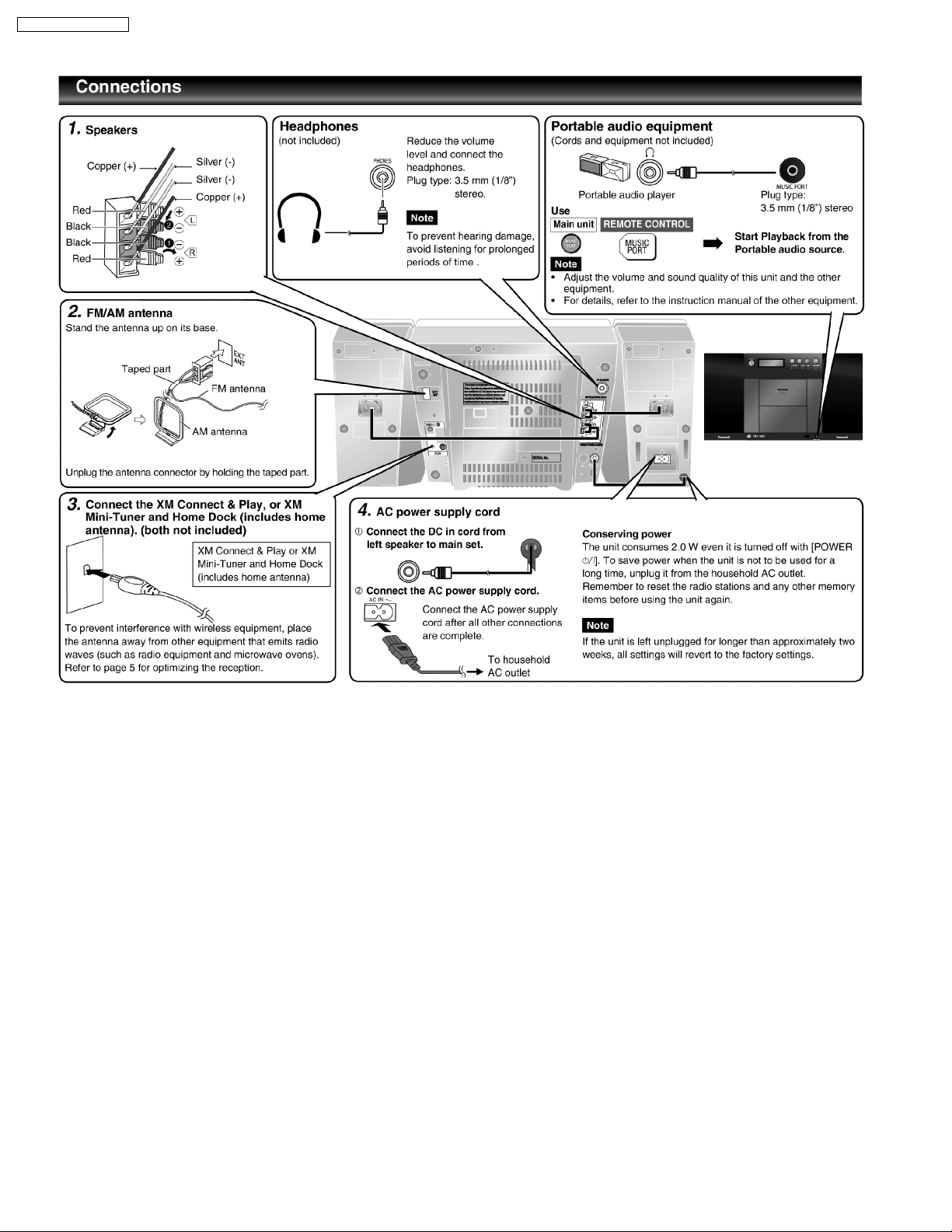
7 Operation Procedures
7.1. Remote Control Key Buttons Operations
7.2. Main Unit Key Buttons Operations
7.3. Connection
7.4. Using the XMョ Satellite Radio
8 Self diagnosis and special mode setting
8.1. Service Mode Summary Table
8.2. Service Mode Table 1
8.3. Error Code Table 1
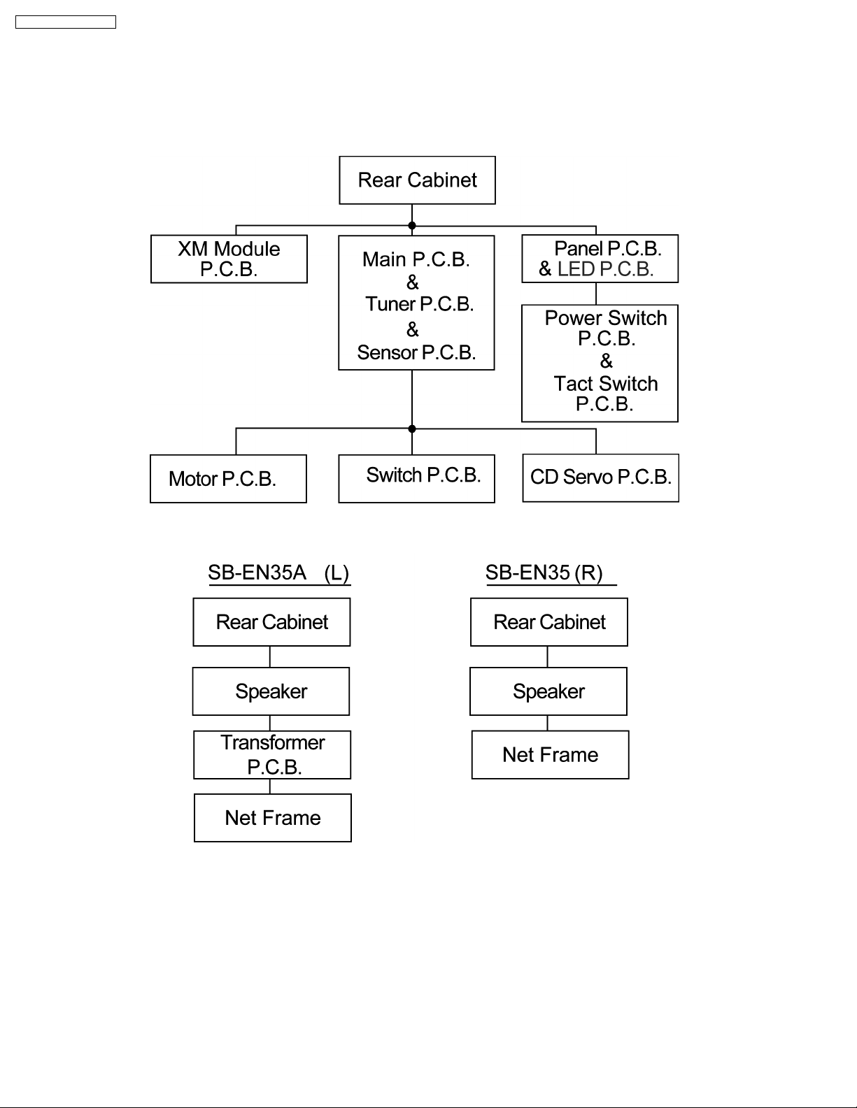
9 Assembling and Disassembling
9.1. Caution
9.2. Disassembly flow chart
9.3. Main Components & P.C.B. Locations
9.4. Disassembly of Rear Cabinet
9.5. Disassembly of XM Module P.C.B.
9.6. Disassembly of Panel P.C.B. & LED P.C.B.
9.7. Disassembly of Main P.C.B., Sensor P.C.B. & Tuner
P.C.B.
9.8. Disassembly of Switch P.C.B. & Traverse Unit
9.9. Disassembly of Power Switch P.C.B. & Tact Switch P.C.B.
9.10. Replacement of Traverse Cover
9.11. Disassembly of CD Servo P.C.B.
9.12. Disassembly of Motor Unit & Motor P.C.B.
4
4
5
5
5
5
6
7
7
9
9
10
11
11
11
12
13
14
14
14
17
19
19
20
21
22
22
22
23
23
24
24
25
26
9.13. Disassembly of CD Block & CD Lid
9.14. Disassembly of Speakers
10 Service Fixture and Tools
11 Service Positions
11.1. Check and Repair of CD Servo P.C.B.
11.2. Check and repair of Main P.C.B., Sensor P.C.B., Tuner
P.C.B., Motor P.C.B., Panel P.C.B., LED P.C.B., Power
Switch P.C.B., Tact Switch P.C.B., XM Module P.C.B. &
Switch P.C.B.
12 Voltage and Waveform Chart
12.1. Main P.C.B.
12.2. CD Servo P.C.B.
12.3. Motor P.C.B.
12.4. Panel P.C.B.
12.5. Tuner P.C.B.
12.6. Waveform Chart
13 Wiring Connection Diagram
14 Block Diagram
14.1. CD Servo
14.2. XM Module & Tuner
14.3. Main (1/2), Transformer, & Sensor
14.4. Main (2/2), Panel, LED, Power Switch, Tact Switch, Switch
& Motor
15 Notes of Schematic Diagrams
16 Schematic Diagram
16.1. (A) CD Servo Circuit
16.2. (B) XM Module Circuit
16.3. (C) Tuner Circuit
16.4. (D) Main Circuit
16.5. (E) Panel Circuit, (F) LED Circuit, (G) Power Switch
Circuit, (H) Tact Switch Circuit & (I) Switch Circuit
16.6. (J) Motor Circuit, (K) Sensor Circuit & (L) Transforme r
Circuit
17 Printed Circuit Board
17.1. (A) CD Servo P.C.B., (B) XM Module P.C.B. & (C) Tuner
P.C.B.
17.2. (D) Main P.C.B.
2.0 W (appx.)
27
28
31
31
32
33
34
34
35
35
35
35
36
37
39
39
40
41
42
43
45
46
47
48
49
52
53
55
56
57
2
Page 3

17.3. (E) Panel P.C.B., (F) LED P.C.B., (G) Power Switch
P.C.B., (H) Tact Switch P.C.B., (I) Switch P.C.B., (J) Motor
P.C.B., (K) Sensor P.C.B. & (L) Transformer P.C.B.
18 Illustration of ICs, Transistors and Diodes
19 Terminal Function of IC's
19.1. IC801 (MN101EF16ZXW) Servo Processor, Digital Signal
Processor/Digital filter and D/A Converter
20 Exploded Views
58
59
60
20.1. Cabinet Parts Location
20.2. Packaging
21 Replacement Parts List
SC-EN35P / SC-EN35 PC
60
61
63
65
67
3
Page 4
SC-EN35P / SC-EN35 PC
1 Safety Precautions
1.1. General Guidelines
1. When servicing, observe the original lead dress. If a short circuit is found, replace all parts which have been overheated or
damaged by the short circuit.
2. After servicing, ensure that all the protective devices such as insulation barriers and insulation papers shields are properly
installed.
3. After servicing, check for leakage current checks to prevent from being exposed to shock hazards.
(This “Safety Precaution” is applied only in U.S.A.)
1. Before servicing, unplug the power cord to prevent an electric shock.
2. When replacing parts, use only manufacturer’s recommended components for safety.
3. Check the condition of the power cord. Replace if wear or damage is evident.
4. After servicing, be sure to restore the lead dress, insulation barriers, insulation papers, shields, etc.
5. Before returning the serviced equipment to the customer, be sure to make the following insulation resistance test to prevent the
customer from being exposed to a shock hazard.
1.1.1. Leakage Current Cold Check
1. Unplug the AC cord and connect a jumper between the two prongs on the plug.
2. Using an ohmmeter measure the resistance value, between the jumpered AC plug and each exposed metallic cabinet part on
the equipment such as screwheads, connectors, control shafts, etc. When the exposed metallic part has a return path to the
chassis, the reading should be between 1MΩ and 5.2MΩ.
When the exposed metal does not have a return path to the chassis, the reading must be
.
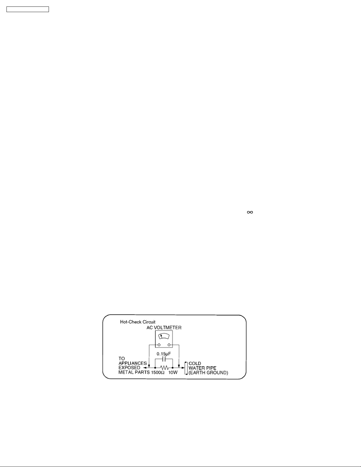
1.1.2. Leakage Current Hot Check (See Figure 1)
1. Plug the AC cord directly into the AC outlet. Do not use an isolation transformer for this check.
2. Connect a 1.5kΩ, 10 watts resistor, in parallel with a 0.15µF capacitor, between each exposed metallic part on the set and a
good earth ground such as a water pipe, as shown in Figure 1.
3. Use an AC voltmeter, with 1000 ohms/volt or more sensitivity, to measure the potential across the resistor.
4. Check each expose d metallic part, and measure the voltage at each point.
5. Reverse the AC plug in the AC outlet and repeat each of the above measurements.
6. The potential at any point should not exceed 0.75 volts RMS. A leakage current tester (Simpson Model 229 or equivalent) may
be used to make the hot checks, leakage current must not exceed 1/2 milliamp. Should the measurement is out of the limits
specified, there is a possibility of a shock hazard, and the equipment should be repaired and rechecked before it is returned to
the customer.
Fig. 1
4
Page 5
SC-EN35P / SC-EN35 PC
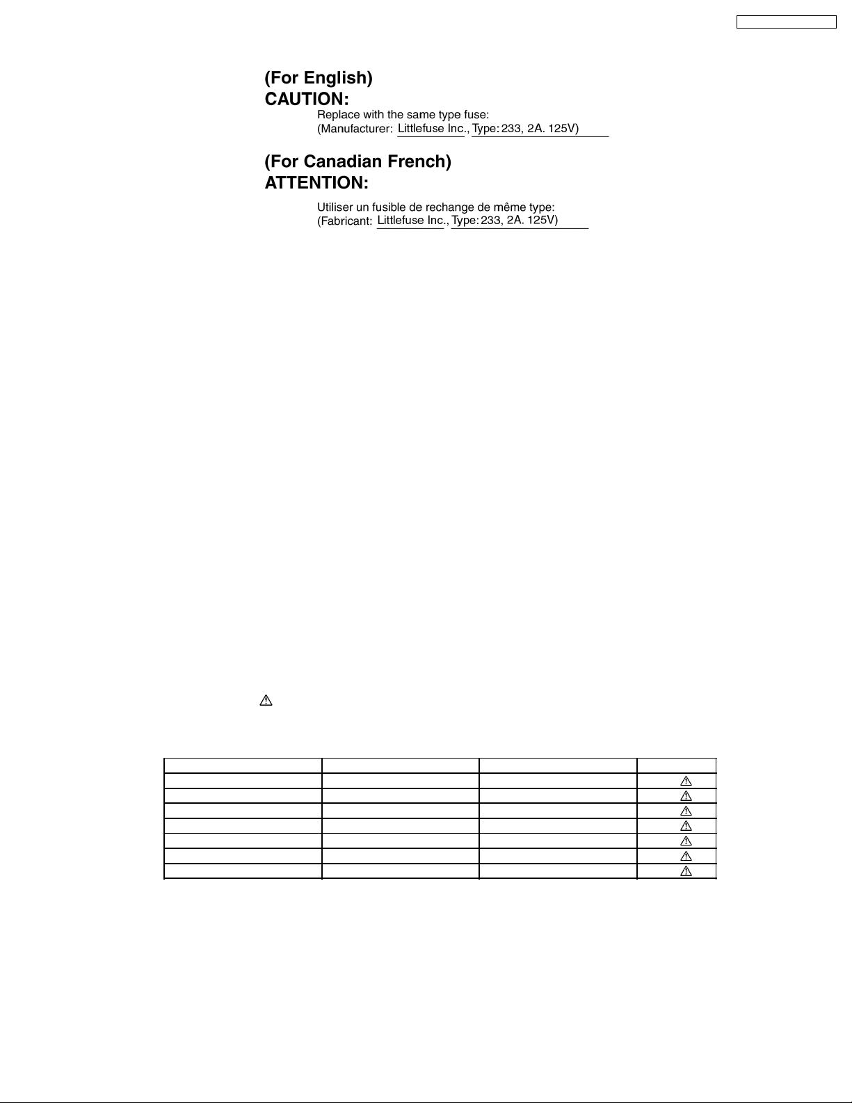
1.2. Caution for fuse replacement
1.3. Before repair and adjustment
Disconnect AC power, discharge Power Capacitors C611 and C616 through a 10Ω, 1W resistor to ground.
DO NOT SHORT-CIRCUIT DIRECTLY (with a screwdriver blade, for instance), as this may destroy solid state devices.
After repairs are completed, restore power gradually using a variac, to avoid overcurrent.
Current consum ption at AC 120V, 60 Hz in NO SIGNAL mode (volume min at CD mode) should be ~ 135mA .
1.4. Protection Circuitry
The protection circuitry may have operated if either of the following conditions are noticed:
· No sound is heard when the power is turned on.
· Sound stops during a performance.
The function of this circuitry is to prevent circuitry damage if, for example, the positive and negative speaker connection wires are
“shorted”, or if speaker systems with an impedance less than the indicated rated impedance of the amplifier are used.
If this occurs, follow the procedure outline s below:
1. Turn off the power.
2. Determine the cause of the problem and correct it.
3. Turn on the power once again after one minute.
Note :
When the protection circuitry functions, the unit will not operate unless the power is first turned off and then on again.
1.5. Safety Parts Information
Safety Parts List:
There are special components used in this equipment which are important for safety.
These parts are marked by
should be replaced with manufacturer’s specified parts to prevent shock, fire or other hazards. Do not modify the original design
without permission of manufacturer.
Reference No. Part No. Part Name & Description Remarks
A2 K2CB2CB00018 AC CORD [M]
F901 K5D202APA008 FUSE [M]
IP601 K5G302AA0002 FUSE PROTECTOR [M]
IP602 K5G251A00008 FUSE PROTECTOR [M]
JK901 K2AB2B000007 FUSE [M]
L901 ELF15N035AN LINE FILTER [M]
T901 G4C5ABD00006 TRANSFORMER [M]
in the Schematic Diagrams & Replac ement Parts List. It is essential that these critical parts
Table 1
5
Page 6

SC-EN35P / SC-EN35 PC
2 Prevention of Electro Static Discharge (ESD) to
Electrostatically Sensitive (ES) Devices
Some semiconductor (solid state) devices can be damaged easily by electricity. Such components commonly are called
Electrostatically Sensitive (ES) Devices. Examples of typical ES devices are integrated circuits and some field-effect transistors and
semiconductor “chip” components. The following techniques should be used to help reduce the incidence of component damage
caused by electro static discharge (ESD).
1. Immediately before handling any semiconductor component or semiconductor-equiped assembly, drain off any ESD on your
body by touching a known earth ground. Alternatively, obtain and wear a commercially available discharging ESD wrist strap,
which should be removed for potential shock reasons prior to applyin g power to the unit under test.
2. After removing an electrical assembly equiped with ES devices, place the assembly on a conductive surface such as aluminium
foil, to prevent electrostatic charge build up or exposu re of the assembly.
3. Use only a grounded-tip soldering iron to solder or unsolder ES devices.
4. Use only an anti-static solder remover device. Some solder removal devices not classified as “anti-static (ESD protected)” can
generate electrical charge to damage ES devices.
5. Do not use freon-propelle d chemicals. These can generate electrical charges sufficient to damage ES devices.
6. Do not remove a replacement ES device from its protective package until immediately before you are ready to install it. (Most
replacement ES devices are packaged with leads electrically shorted together by conductive foam, aluminium foil or
comparable conductive material).
7. Immediately before removing the protective material from the leads of a replacement ES device, touch the protective material
to the chassis or circuit assembly into which the device will be installed.
Caution
Be sure no power is applied to the chassis or circuit, and observe all other safety precautions.
8. Minimize body motions when handling unpackaged replacement ES devices. (Otherwise harmless motion such as the brushing
together of your clothes fabric or the lifting of your foot from a carpeted floor can generate static electricity (ESD) sufficient to
damage an ES device).
6
Page 7
SC-EN35P / SC-EN35 PC
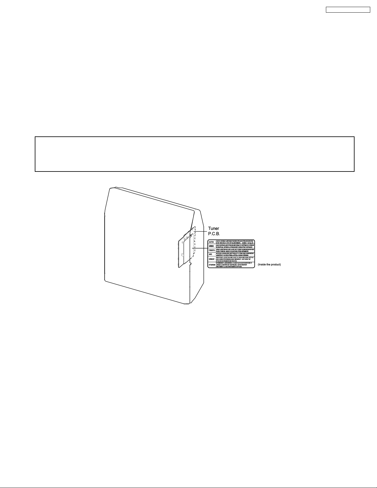
3 Precaution of laser diode
CAUTION:
This unit utilizes a class 1 laser diode in the optical pickup unit .
Invisible laser radiation is emitted from the optical pickup lens.
Wavelength: 780nm
When the unit is turned on:
1. Do not look directly into the optical pickup lens.
2. Do not use optical instruments to look at the optical pickup lens.
3. Do not adjust the preset variable resistor on the optical pickup lens.
4. Do not disassemble the optical optical pickup unit.
5. If the optical pickup is replaced, use the manufacturer’s specified replacement pickup only.
6. Use of control or adjustments or performance of procedures other than those specified herein may result in hazardous radiation
exposure.
CAUTION!
THIS PRODUCT UTILIZES A LASER.
USE OF CONTROLS OR ADJUSTMENTS OR PERFORMANCE OF PROCEDURES OTHER THAN THOSE SPECIFIED HEREIN MAY RESULT
IN HAZARDOUS RADIATION EXPOSURE.
n Use of caution label (Except for U.S.A.)
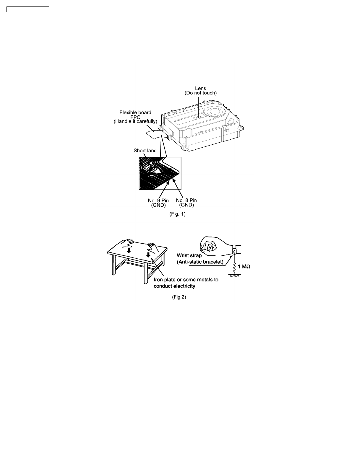
4 Handling Precautions For Traverse Unit
The laser diode in the traverse deck (optical pickup) may break down due to potential difference caused by the static electricity of
clothes or our human body.
So, be careful of electrostatic breakdown during repair of the traverse deck (optical pickup).
· Way of handling the traverse deck (optical pickup)
1. Do not subject the traverse deck (optical pickup) to static electricity as it is extremely sensitive to electrical shock.
2. To prevent the breakdown of the laser diode, an antistatic shorting pin is inserted into the flexible board (FFC board). (Fig. 1)
3. Take care not to apply excessive stress to the flexible board (FFC board). When removing or connecting the short pin, finish
the job in as short time as possible.
4. Do not turn the variable resistor (laser power adjustment). It has already been adjusted.
Grounding for electrostatic breakdown prevention
1. Human body grounding. (Fig. 2)
Use the anti-static wrist strap to discharge the static electricity from your body.
2. Work table grounding. (Fig. 2)
Put a conductive material (sheet) or steel sheet on the area where the traverse deck (optical pickup) is place, and ground the
sheet.
7
Page 8
SC-EN35P / SC-EN35 PC
Caution :
The static electricity of your clothes will not be grounded through the wrist strap. So, take care not to let your clothes touch the
traverse deck (optical pickup).
Caution when replacing the Traverse Deck
The traverse deck has a short point shorted with solder to protect the laser diode against electrostatics breakdown. Be sure to
remove the solder from the short point before making connections.
8
Page 9

SC-EN35P / SC-EN35 PC
5 About Lead Free Solder (PbF)
5.1. Service caution based on legal restrictions
5.1.1. General description about Lead Free Solder (PbF)
The lead free solder has been used in the mounting process of all electrical components on the printed circuit boards used for this
equipment in considering the globally environmental conservation.
The normal solder is the alloy of tin (Sn) and lead (Pb). On the other hand, the lead free solder is the alloy mainly consists of tin
(Sn), silver (Ag) and Copper (Cu), and the melting point of the lead free solder is higher approx.30 degrees C (86°F) more than that
of the normal solder.
Definition of PCB Lead Free Solder being used
The letter of “PbF” is printed either foil side or components side on the PCB using the lead free solder.
(See right figure)
Service caution for repair work using Lead Free Solder (PbF)
· The lead free solder has to be used when repairing the equipment for which the lead free solder is used.
(Definition: The letter of “PbF” is printed on the PCB using the lead free solder.)
· To put lead free solder, it should be well molten and mixed with the original lead free solder.
· Remove the remaining lead free solder on the PCB cleanly for soldering of the new IC.
· Since the melting point of the lead free solder is higher than that of the normal lead solder, it takes the longer time to melt
the lead free solder.
· Use the soldering iron (more than 70W) equipped with the temperature control after setting the temperature at 350±30
degrees C (662±86°F).
Recommended Lead Free Solder (Service Parts Route.)
· The following 3 types of lead free solder are available through the service parts route.
RFKZ03D01K-----------(0.3mm 100g Reel)
RFKZ06D01K-----------(0.6mm 100g Reel)
RFKZ10D01K-----------(1.0mm 100g Reel)
Note
* Ingredient: tin (Sn), 96.5%, silver (Ag) 3.0%, Copper (Cu) 0.5%, Cobalt (Co) / Germanium (Ge) 0.1 to 0.3%
9
Page 10
SC-EN35P / SC-EN35 PC
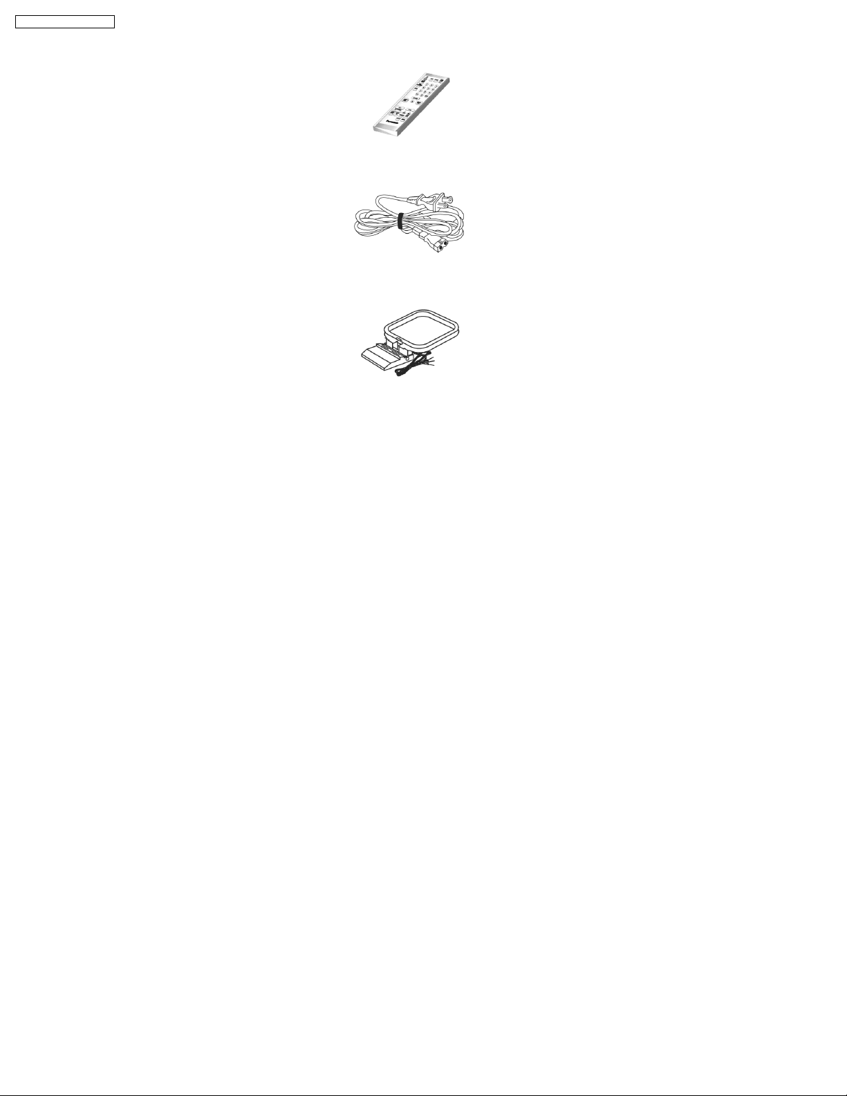
6 Accessories
Remote Control
AC Cord
FM/AM Antenna
10
Page 11
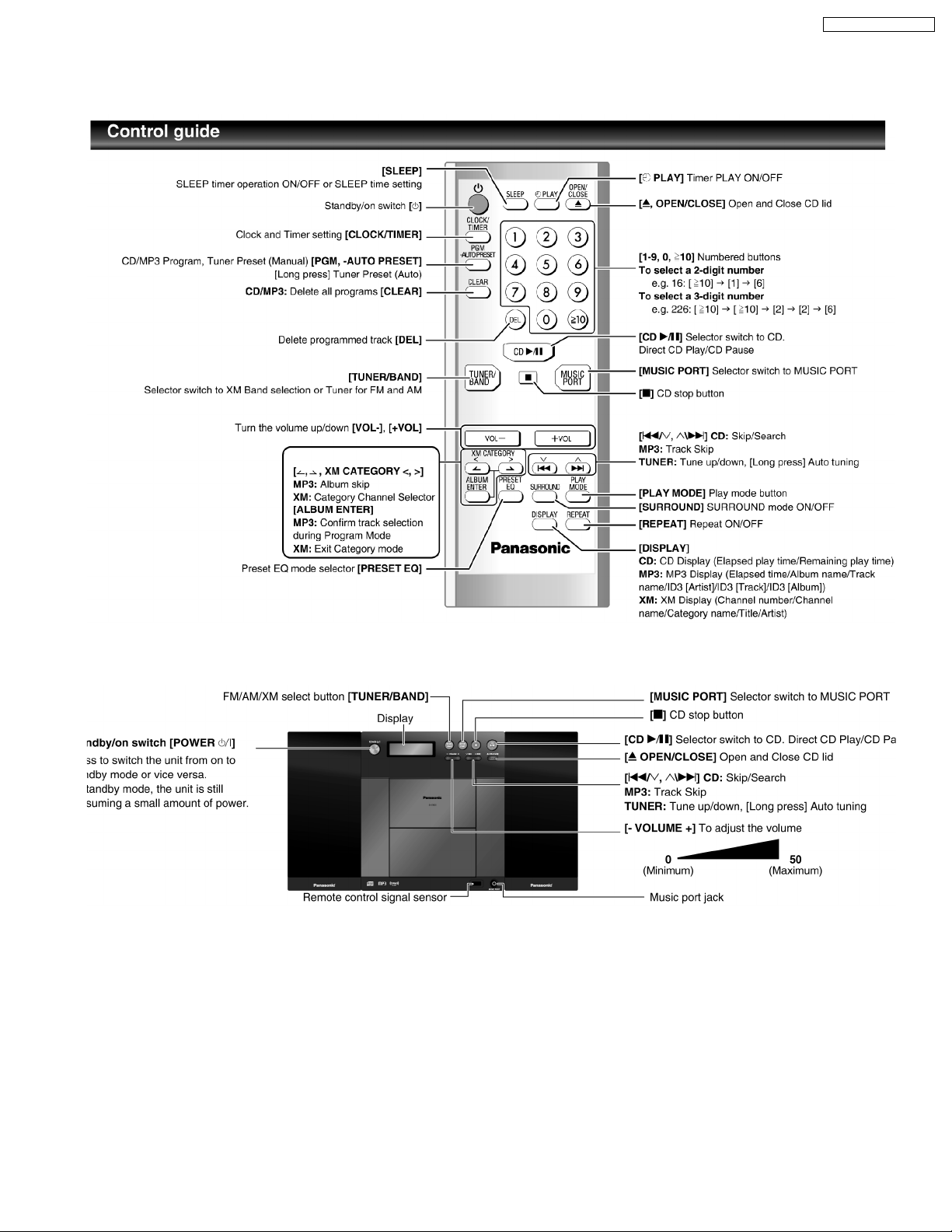
7 Operation Procedures
7.1. Remote Control Key Buttons Operations
SC-EN35P / SC-EN35 PC
7.2. Main Unit Key Buttons Operations
11
Page 12
SC-EN35P / SC-EN35 PC
7.3. Connection
12
Page 13
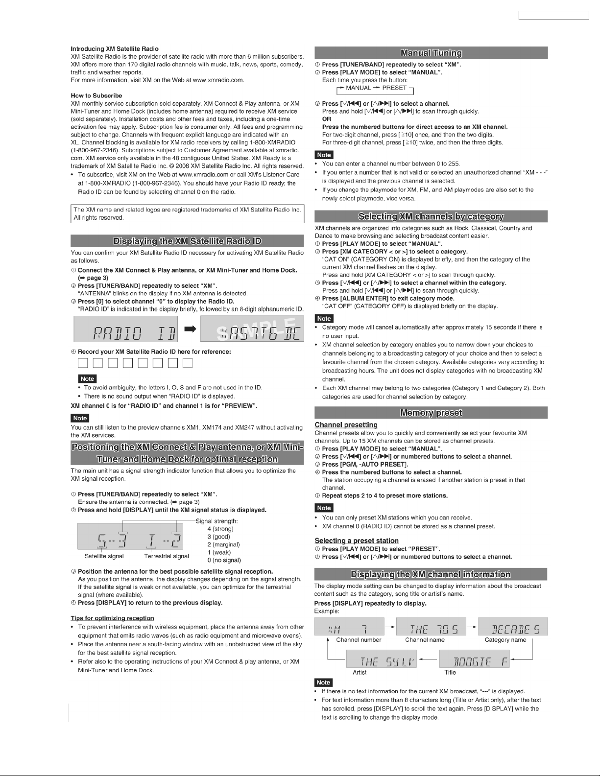
7.4. Using the XM® Satellite Radio
SC-EN35P / SC-EN35 PC
13
Page 14
SC-EN35P / SC-EN35 PC
8 Self diagnosis and special mode setting
This unit is equipped with feature s of self-diagnostic & special mode setting for checking the functions & reliability.
8.1. Service Mode Summary Table
The service mode can be activated by pressing various button combination on the main unit and remote control unit. Below is the
summary for the various modes for checking:-
Player buttons Remote control unit buttons Application Note
[ ] [4], [7] To enter into doctor mode for various item
checking.
Mode Remote control unit buttons Application Note
Doctor Mode [DIMMER] FL ALL Segment inspection (Refer to the section 8.2 for more
[7], [8], [9] Forced VOL setting (Refer to the section 8.2 for more
[ ], [1], [1] CD Loading Test (Refer to the section 8.2 for more
[ ], [1], [2] CD Traverse Test (Refer to the section 8.2 for more
[ ], [1], [3] CD Combination Test (Refer to the section 8.2 for more
[ ], [1], [4] CD Auto Adjustment Display (Refer to the section 8.2 for more
[SLEEP] Cold Start setting (Refer to the section 8.2 for more
(Refer to the section 8.2 for more
information.)
information.)
information.)
information.)
information.)
information.)
information.)
information.)
8.2. Service Mode Table 1
Below is the various special modes for checking:-
Item FL Display Key Operation
Mode Name Description Front Key
Self-Diagnostic
Mode
To enter into self diagnostic checking
for main unit.
1. Select [CD] for CD mode (Ensure
no CD inserted.)
2. Press and hold [
seconds follow by [FF]
To exit, press [
main unit or remote control.
] button for 2
] button on
14
Page 15
Item FL Display Key Operation
Mode Name Description Front Key
Doctor Mode To enter into Doctor Mode for
checking of various items and
displaying EEPROM and firmware
version.
Note: The micro-processor version as
shown is an example. It will be revise
when there is an updates.
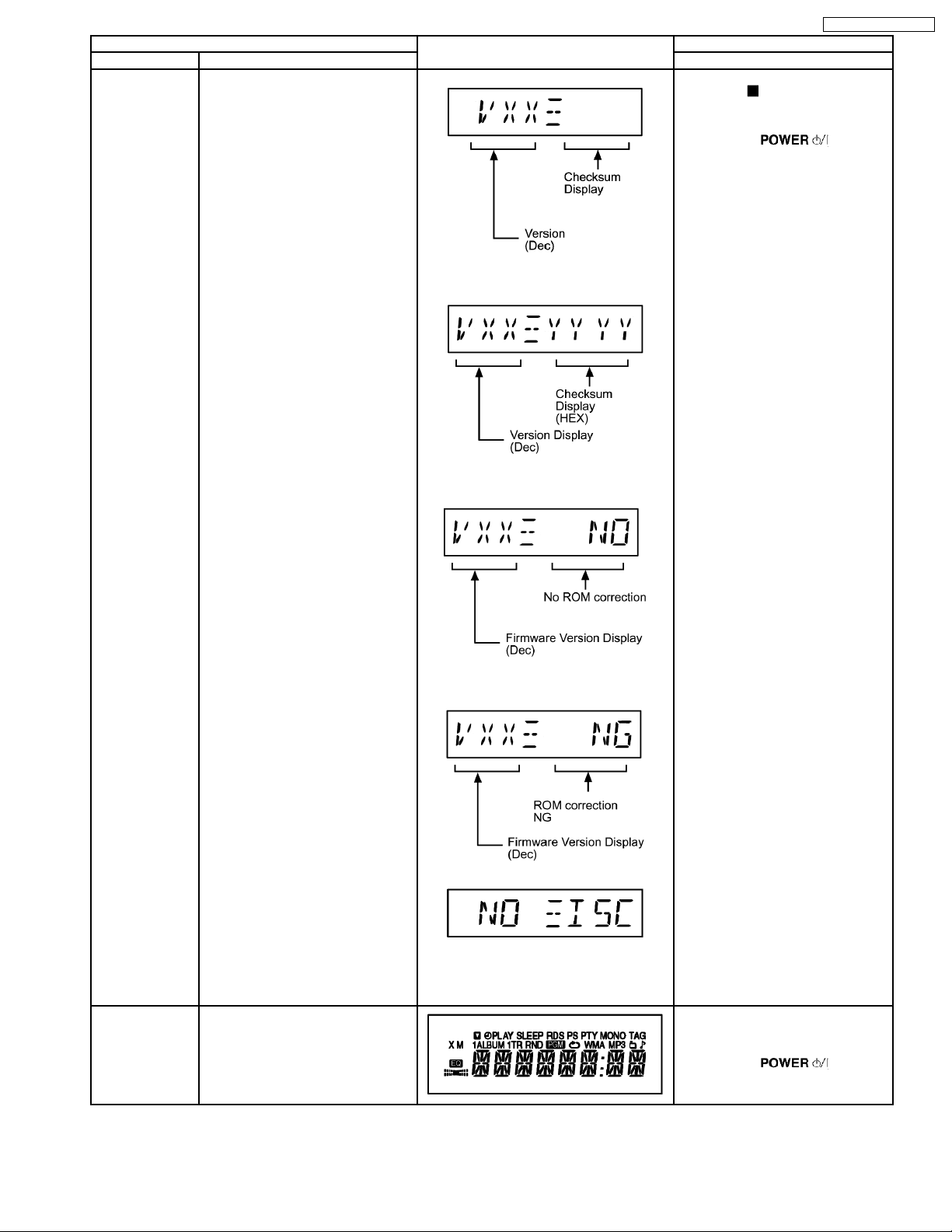
DIsplay 1
In any mode:
1. Press [
follow by [4] and [7] on remote
control.
To exit, press [
main unit or remote control.
FL Display sequence
Display 1 → 2
Checksum (Condition 1)
When EEPROM IC detected and has ROM
correction.
Checksum (Condition 2)
When EEPROM IC is detected and there is
no ROM correction.
SC-EN35P / SC-EN35 PC
] button on main unit
] button on
FL Display Test To check the FL segments display (All
segments will light up)
Checksum (Condition 3)
When EEPROM IC is detected and has ROM
correction but not working properly.
Display 2
The Check Sum of EEPROM and firmware
version will be display for 1 sec.
* ROM correction
** Firmware version No:
In doctor mode:
1. Press [DIMMER] button on remote
control.
To exit, press [
] button on
main unit or remote control.
15
Page 16
SC-EN35P / SC-EN35 PC
Mode Name Description Front Key
Volume Setting
Mode
Item FL Display Key Operation
To check for the volume setting of the
main unit. The volume will be
automatically set to its respective
level (in dB). During the mode,
trebble/bass/EQ will be set to “0” dB
& OFF.
In doctor mode:
1. Press [7] button on remote control.
2. Press [8] button on remote control.
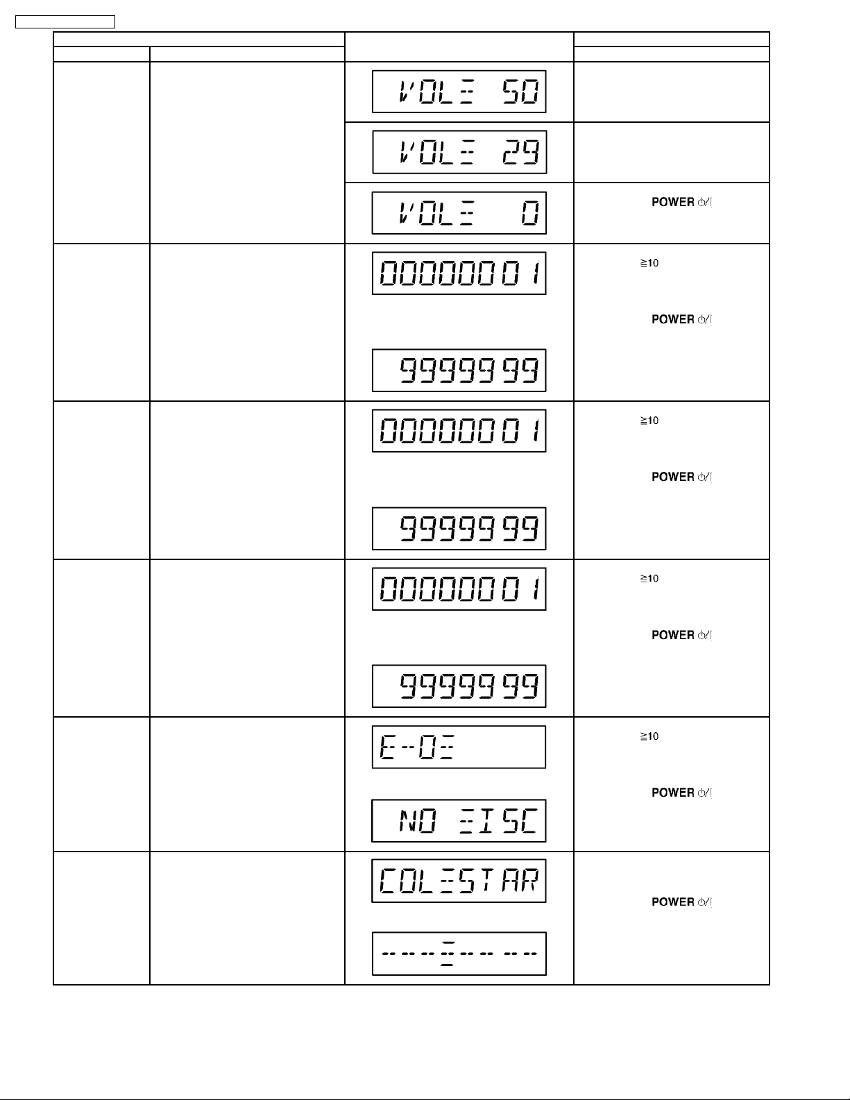
CD Loading Test
Mode
CD Traverse Unit
Test Mode
CD Combination
Test Mode
To determine the reliability of CD
Loading unit.
To check for the Open/Close
operation for the CD loading unit. It
fails when there is abnormality in
opening or closing.
To check for the traverse unit
operation. In this mode, the first & last
track is access & read. (TOC). It fails
when TOC is not completed by IOS or
the traverse is out of focus.
A combination of CD loading &
traverse unit test.
The counter will increment by 1 until reach
9999999
↓
The counter will increment by 1 until reach
9999999
↓
The counter will increment by 1 until reach
9999999
↓
3. Press [7] button on remote control.
To exit, press [
main unit or remote control.
In doctor mode:
1. Press [
remote control.
To cancel, press [0] button remote
control.
To exit, press [
main unit or remote control.
In doctor mode:
1. Press [
remote control.
To cancel, press [0] button remote
control.
To exit, press [
main unit or remote control.
In doctor mode:
1. Press [
remote control.
To cancel, press [0] button remote
control.
To exit, press [
main unit or remote control.
], [1] & [1] button on
], [1] & [2] button on
], [1] & [3] button on
] button on
] button on
] button on
] button on
CD Auto
Adjustment
Display
Cold Start To activate cold start upon next AC
To display result of self adjustment for
CD.
For more information, please refer to
Section 8.2.1.
The [NO DISC] display will appear after 3s,
power up.
8.2.1. CD Self-Adjustment (AJST) Result Display
Purpose: To display result of self-adjustment for CD.
16
In doctor mode:
1. Press [
remote control.
To cancel, press [0] button remote
control.
To exit, press [
main unit or remote control.
In doctor mode:
1. Press [SLEEP] button on remote
control.
To exit, press [
↓
main unit or remote control.
], [1] & [4] button on
] button on
] button on
Page 17
Below is the procedures for this mode.
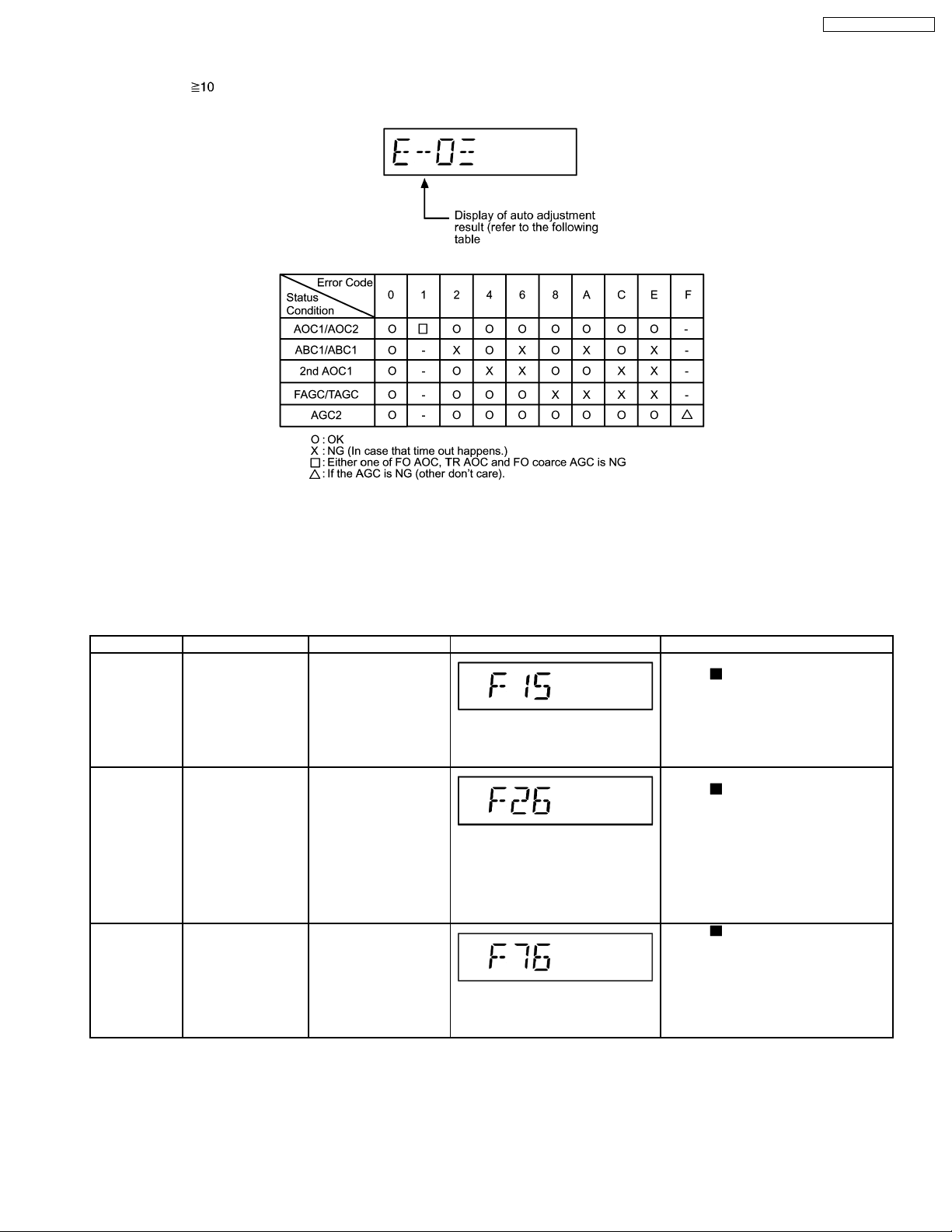
Step 1: Enter into Doctor mode (For more information refer to section 8.2 on key operation to enter into this mode).
Step 2: When [
], [1] & [4] are pressed at the doctor mode, the following shall be display ed for 3s. The result shall correspond
to the condition met as shown in the table below:
SC-EN35P / SC-EN35 PC
8.3. Error Code Table 1
8.3.1. Mechanism Error Code Table
Self-Diagnosis Function provides information on any problems occuring for the unit and its respective components by displaying
error codes. These error code such as U**, H** and F** are stored in memory and held unless it is cleared.
The error code is automatically display after entering into self-diagnostic mode.
Error Code Diagnosis Contents Description of error Automatic FL Display Remarks
F15 CD REST SW
abnormal
F26 Communication
between CD servo
LSI and micro-p
abnormal.
F76 Abnormality in the
output voltage of
stabilized power
supply.
CD traverse position
initial setting operation
failsafe counter
(1000ms) waiting for
REST SW to turn on.
Error no. shall be clear
by force or during cold
start.
CD function DTMS
command, after system
setting, if SENSE = “L”
cannot be detected.
Memory shall contain
F26code. After power
on, CD function shall
continue, error display
shall be “NO DISC”.
Error no. shall be clear
by force or cold start.
In normal operation
when “DCDET” is
detected “L” (IOIO) for
two consecutive times,
this error code will be
displayed for 2s & after
PCONT will be turned to
“L” (Low).
For CD unit.(For traverse).
Press [
For CD unit.(For traverse).
Press [
Press [ ] on main unit for next error.
] on main unit for next error.
] on main unit for next error.
17
Page 18
SC-EN35P / SC-EN35 PC
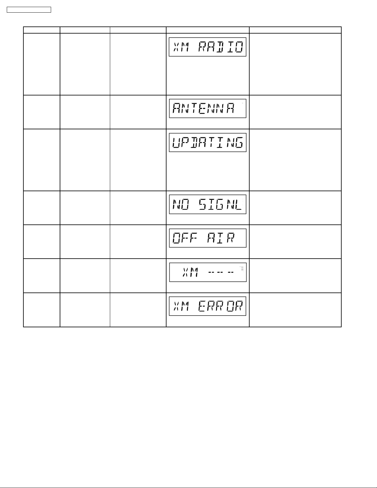
8.3.2. XM Satellite Radio Code Table
Error Code Diagnosis Contents Description of error Automatic FL Display Remarks
XM RADIO XM Radio Selection It takes a short time for
ANTENNA XM connectivity The XM antenna is not
UPDATING XM Encryption Code 1) The XM antenna is
NO SIGNAL XM Signal receptivity The XM antenna is too
OFF AIR XM Channel
Broadcasting
the XM radio to power up
after selecting the
source on the main unit.
During this time, the FL
display shows the
message. Wait for a few
seconds for the process
to complete, if not, check
on the XM antenna if it is
connected or damaged.
properly connected or
the antenna cable is
damaged.
being updated with the
latest encryption code.
(Wait for few seconds for
the updating to be
completed.)
2) The selected XM
channel has been
blocked, or is no longer
available with the
subscription package.
weak.
Re-oriented the XM
antenna for better
reception.
The selected XM
channel is not currently
broadcasting
information.
(Flashing)
For more information, refer to operating
instruction manual for connection of
antenna.
(Flashing)
(Flashing)
For more information, refer to operating
instruction manual for optimizing the
signal reception.
(Flashing)
For more information, refer to operating
instruction manual for selection of the
channels.
(Flashing)
XM --- XM Channel
Broadcasting
XM ERROR XM Module
Abnormality
The selected XM
channel is not available.
Selection of a diffrent
channels.
The XM radio module is
performing abnormally.
Turn the main unit off
and power on. The XM
antenna may be
defective.
(Flashing)
(Flashing)
Special Note: XM Satellite Radio ID is necessary for the activation of the XM Satellite Radio.
For more information, refer to operating
instruction manual for selection of the
channels.
18
Page 19
SC-EN35P / SC-EN35 PC
9 Assembling and Disassembling
9.1. Caution
“ATTENTION SERVICER”
Some chassis components may have sharp edges. Be careful when disassembling and servicing.
1. This section describes procedures for checking the operation of the major printed circuit boards and replacing the main
components.
2. For reassembly after operation checks or replacement, reverse the respective procedures.
Special reassembly procedures are described only when required.
3. Select items from the following index when checks or replacement are required.
4. Refer to the Parts No. on the page of “Parts Location and Replacement Parts List” (Section 21), if necessary.
Warning :-
This product uses a laser diode. Refer to caution statement Precaution of Laser Diode.
Below is the list of disassembly sections
· Disasse mbly of Rear Cabinet
· Disasse mbly of XM Module P.C.B.
· Disasse mbly of Panel P.C.B. & LCD P.C.B.
· Disasse mbly of Main P.C.B., Sensor P.C.B. & Tuner P.C.B.
· Disasse mbly of Switch P.C.B. & Traverse Unit
· Disasse mbly of Power Switch P.C.B. & Tact Switch P.C.B.
· Replacement of Traverse Cover
· Disasse mbly of CD Servo P.C.B.
· Disasse mbly of Motor Unit & Motor P.C.B.
· Disasse mbly of CD Block & CD Lid
· Disasse mbly of Speak ers
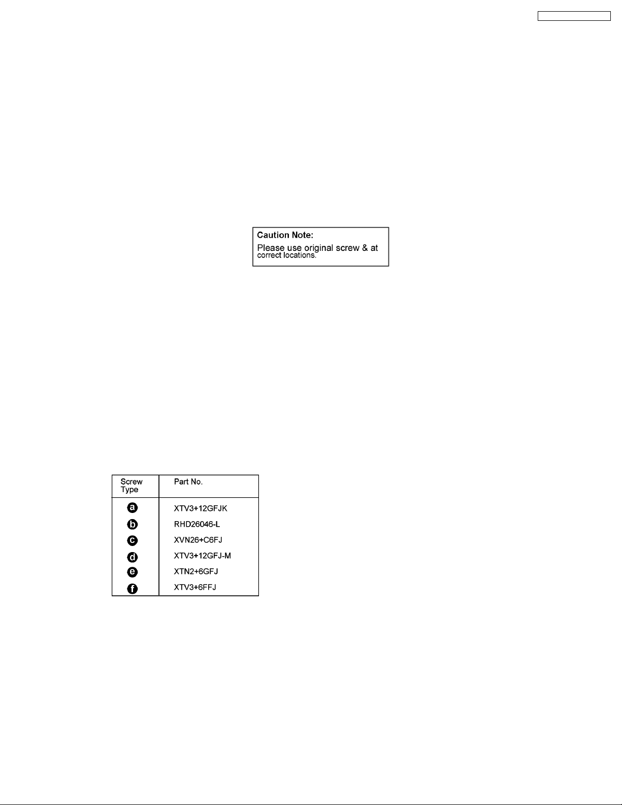
Below shown is part no. of different screws types used:
19
Page 20
SC-EN35P / SC-EN35 PC
9.2. Disassembly flow chart
The following chart is the procedure for disassembling the casing and inside parts for internal inspection when carrying out the
servicing.
To assemble the unit, reverse the steps shown in the chart as below.
9.2.1. For Main unit
9.2.2. For Speaker unit
20
Page 21
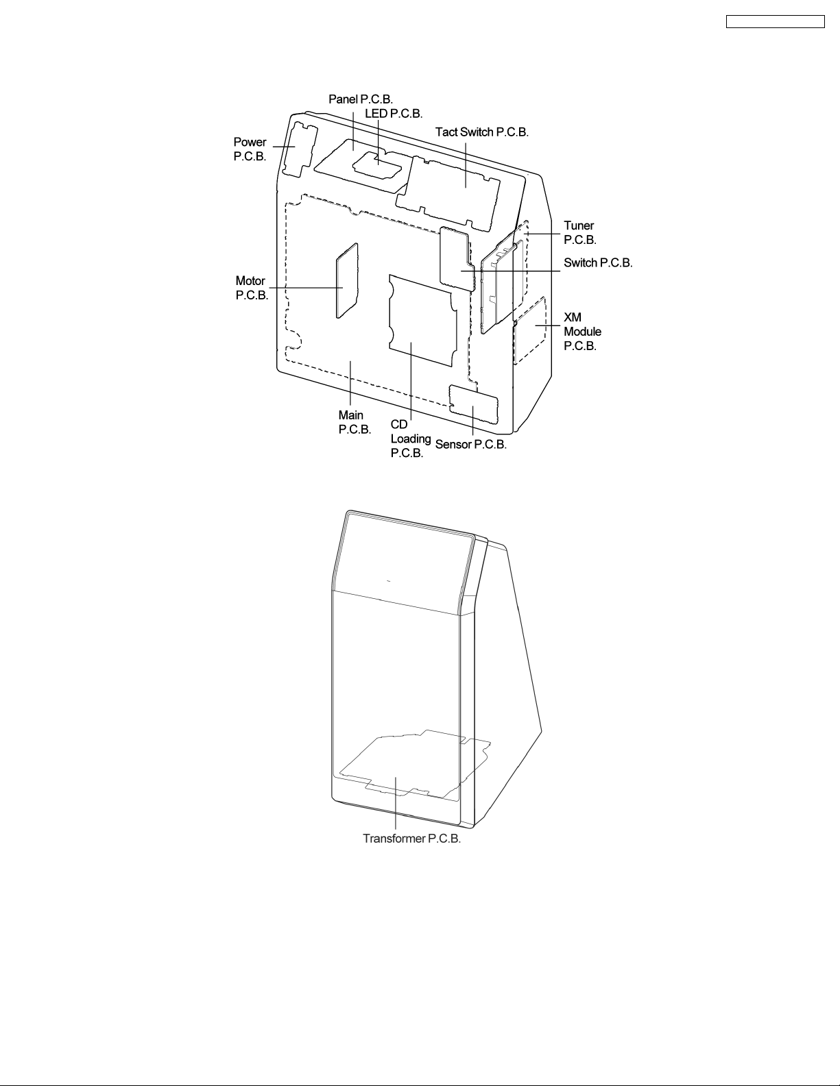
9.3. Main Components & P.C.B. Locations
9.3.1. Main Parts Locations
SC-EN35P / SC-EN35 PC
9.3.2. Speaker Unit Parts Location (For SB-EN35A only)
21
Page 22
SC-EN35P / SC-EN35 PC
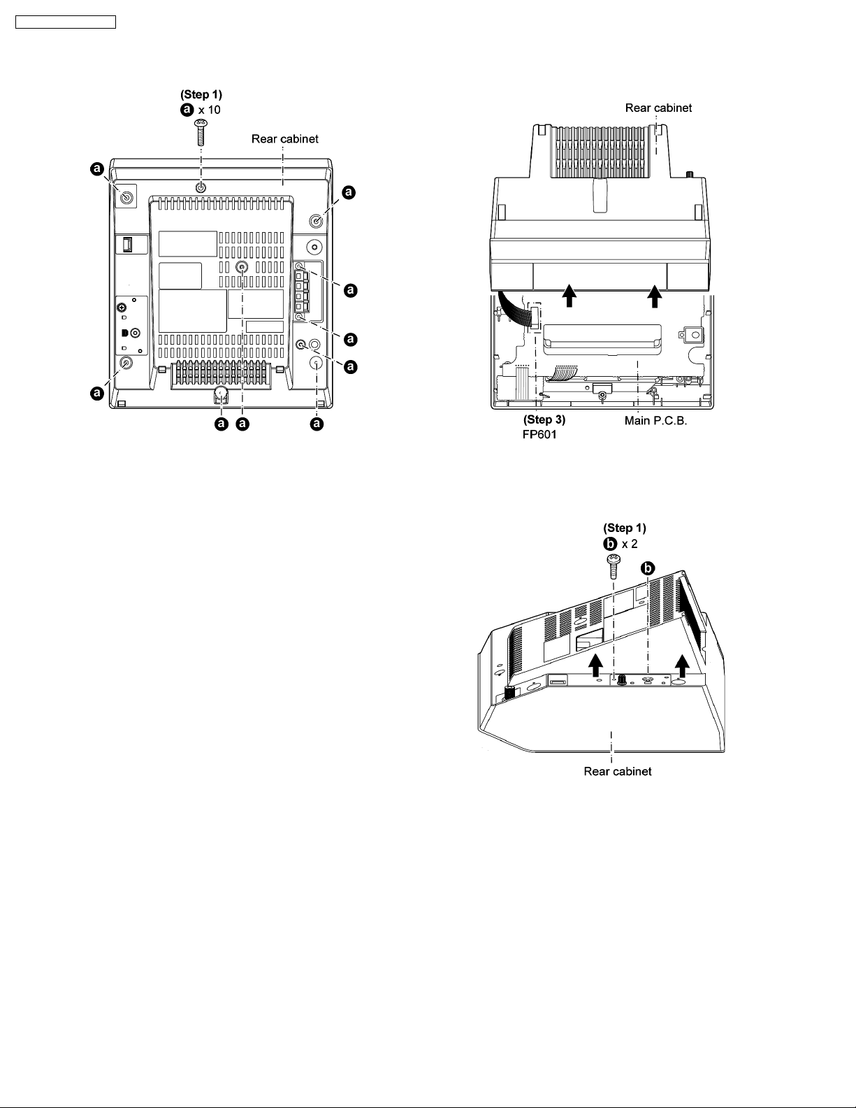
9.4. Disassembly of Rear Cabinet
Step 1 Remove 10 screws.
Step 2 Lift up the rear cabinet.
Step 3 Detach cable (FP601) on Main P.C.B. and remove the
rear cabinet as arrow shown.
9.5. Disassembly of XM Module P.C.B.
· Follow the (Step 1) - (Step 2) of Item 9.4 - Disassembly of Rear Cabinet
Step 1 Remove 2 screws.
9.6. Disassembly of Panel P.C.B. & LED P.C.B.
· Follow the (Step 1) - (Step 2) of Item 9.4 - Disassembly of Rear Cabinet
Step 1 Remove 2 screws on the LCD Holder unit.
22
Page 23

Step 2 Detach cable (P801).
9.7. Disassembly of Main P.C.B., Sensor P.C.B. & Tuner P.C.B.
· Follow the (Step 1) - (Step 2) of Item 9.4 - Disassembly of Rear Cabinet
Step 1 Remove 5 screws.
Step 2 Detach cables (P352, P351 ,FP701 ,P801 & P802) on
Main P.C.B..
Step 3 Lift up the Main P.C.B. Sensor P.C.B. and Tuner P.C.B.
SC-EN35P / SC-EN35 PC
9.8. Disassembly of Switch P.C.B. & Traverse Unit
· Follow the (Step 1) - (Step 3) of Item 9.4 - Disassembly of Rear Cabinet
· Follow the (Step 1) - (Step 3) of Item 9.7 - Disassembly of Main P.C.B., Sensor P.C.B. & Tuner P.C.B.
Step 1 Remove 4 screws.
Step 2 Remove 2 screws on Switch P.C.B..
23
Page 24

SC-EN35P / SC-EN35 PC
9.9. Disassembly of Power Switch P.C.B. & Tact Switch P.C.B.
· Follow the (Step 1) - (Step 3) of Item 9.4 - Disassembly of Rear Cabinet
· Follow the (Step 1) - (Step 2) of Item 9.6 - Disassembly of Panel P.C.B. & LED P.C.B.
Step 1 Detach cable (P802) on Main P.C.B..
Step 2 Remove 3 screws.
Step 3 Release 1 claw to remove front ornament.
Step 4 Release 6 catches to remove Power P.C.B. & Tact
Switch P.C.B..
· Assemble of Front Ornament into slot.
Ensure front ornament fully insert to front cabinet.
9.10. Replacement of Traverse Cover
· Follow the (Step 1) - (Step 3) of Item 9.4 - Disassembly of Rear Cabinet
· Follow the (Step 1) - (Step 2) of Item 9.7 - Disassembly of Main P.C.B. , Sensor P.C.B. & Tuner P.C.B.
· Follow the (Step 1) of Item 9.8 - Disassembly of Switch P.C.B. & Traverse Unit
Step 1 Release 3 catches and remove the Traverse Cover.
24
Page 25

Step 2 Pull out FFC.
SC-EN35P / SC-EN35 PC
Step 3 Widening the catch, push the fixed pin in. (a) → (b)
Step 4 Lift up the traverse unit to remove it.
Caution:
Keep the floating springs (x 4) in safe place & avoid losing
them.
9.11. Disassembly of CD Servo P.C.B.
· Follow the (Step 1) - (Step 3) of Item 9.4 - Disassembly of Rear Cabinet
· Follow the (Step 1) - (Step 2) of Item 9.7 - Disassembly of Main P.C.B. , Sensor P.C.B. & Tuner P.C.B.
· Follow the (Step 1) of Item 9.8 - Disassembly of Switch P.C.B. & Traverse Unit
· Follow the (Step 1) - (Step 4) of Item 9.10 - Replacement of Traverse Cover
Step 1 Desolder the terminal.
25
Page 26

SC-EN35P / SC-EN35 PC
Step 2 Remove 3 screws.
Step 3 Flip the CD Servo P.C.B. over to one side.
Step 4 Detach FFC out from the connector.
Step 5 Attach a short pin to the unit.
Caution:
Insert a short pin into FFC of the optical pickup. [See “Handling
Precautions for traverse unit”].
9.12. Disassembly of Motor Unit & Motor P.C.B.
· Follow the (Step 1) - (Step 3) of Item 9.4 - Disassembly of Rear Cabinet
· Follow the (Step 1) - (Step 2) of Item 9.7 - Disassembly of Main P.C.B. , Sensor P.C.B. & Tuner P.C.B.
Step 1 Remove 3 screws.
Step 4 Remove the belt.
Step 5 Remove pulley gear, 2nd gear and drive gear.
· Disassembly of motor assembly (gears & belt)
Step 2 Remove motor assembly.
Step 3 Remove 2 screws.
Step 6 Remove 2 screws at motor unit.
Step 7 Remove 1 screw and unsolder 3 points at gear base.
26
Page 27

9.13. Disassembly of CD Block & CD Lid
· Follow the (Step 1) - (Step 3) of Item 9.4 - Disassembly of Rear Cabinet
· Follow the (Step 1) - (Step 2) of Item 9.7 - Disassembly of Main P.C.B. , Sensor P.C.B. & Tuner P.C.B.
· Follow the (Step 1) of Item 9.8 - Disassembly of Switch P.C.B. & Traverse Unit
· Follow the (Step 1) of Item 9.11 - Disassembly of Motor Unit & Motor P.C.B.
Step 1 Remove 6 screws to remove CD Block Unit.
Step 3 Remove 4 screws, remove sw lever (left) and roller
guide (R).
SC-EN35P / SC-EN35 PC
Step 2 Remove 2 screws.
Step 4 Remove cd lid.
27
Page 28

SC-EN35P / SC-EN35 PC
9.14. Disassembly of Speakers
9.14.1. Disassembly of the speaker (SB-EN35) - (R)
Step 1 Remove 6 screws.
Step 2 Remove the back cabinet ass’y..
Step 4 Remove 4 screws.
· Disasse mbly of net frame ass’y
Step 5 Remove 4 screws.
Step 3 Unsolder the lead wires, silver (-) and gold (+).
28
Page 29

9.14.2. Disassembly of the rear cabinet (SB-EN35A) - (L)
SC-EN35P / SC-EN35 PC
Step 1 Remove 6 screws.
Step 2 Remove the back cabinet ass’y..
Step 3 Unsolder the lead wires.
Step 4 Remove 4 screws.
29
Page 30

SC-EN35P / SC-EN35 PC
· Disasse mbly of net frame ass’y
Step 5 Remove 4 screws.
· Remova l of Transformer P.C.B.
Step 1 Remove 1 screw on back cabine t assy.
Step 2 Remove 3 screws to remove the port unit.
Step 3 Remove 4 screws on Transformer P.C.B. unit.
Step 4 Unsolder wire and remove Transformer P.C.B..
30
Page 31

SC-EN35P / SC-EN35 PC
10 Service Fixture and Tools
Service Tools
Extension FFC
(A) CD Servo P.C.B. - Main P.C.B. REEX0485 (14 Pins)
11 Service Positions
General proceduree:
Connect the DC in cord cable from (SB-EN35A) to main set, connect AC power supply cord to speaker to on the set. Load in cd
and switch off the set. Proceed to checking.
Note: For description of the disassembly procedures, see the Section 9.
31
Page 32

SC-EN35P / SC-EN35 PC
11.1. Check and Repair of CD Servo P.C.B.
32
Page 33

SC-EN35P / SC-EN35 PC
11.2. Check and repair of Main P.C.B., Sensor P.C.B., Tuner P.C.B., Motor
P.C.B., Panel P.C.B., LED P.C.B., Power Switch P.C.B., Tact Switch
P.C.B., XM Module P.C.B. & Switch P.C.B.
33
Page 34

SC-EN35P / SC-EN35 PC
12 Voltage and Waveform Chart
Note:
Circuit voltage and waveform described herein shall be regarded as reference information when probing defect point, because it
may differ from an actual measuring value due to difference of Measuring instrument and its measuring condition and product itself.
12.1. Main P.C.B.
34
Page 35

12.2. CD Servo P.C.B.
SC-EN35P / SC-EN35 PC
12.3. Motor P.C.B.
12.4. Panel P.C.B.
12.5. Tuner P.C.B.
35
Page 36

SC-EN35P / SC-EN35 PC
12.6. Waveform Chart
36
Page 37

13 Wiring Connection Diagram
SC-EN35P / SC-EN35 PC
HEADPHONE
SPEAKER
TRANSFORMER
JW806
1
2
PbF
JK601
JK602
JK604
PbF
E
PANEL P.C.B
SOLDER SIDE
1 2
P802
D
P351
5
. . .
1
1 . . . . . 9 1 . 3
P801
MAIN P.C.B
SOLDER SIDE
P352
JW1
17
16
. . . . .
2
1
. . . . . . . . .
11
. . . . . . .
1
FP601
P601
6 . . . . 1
PbF
TRANSFORMER P.C.B
L
SOLDER SIDE
JW802
1 . . . . . . 9
FP701
1 . . . . . . . . . 21
2. . . . . . . . . 22
PbF
JW1
1
. . . . . . . . .
11
TUNER CIRCUIT P.C.B
C
SOLDER SIDE
PbF
XM
JK1
XM MODULE P.C.B
B
SOLDER SIDE
(SIDE B)
1
.
AM/FM
P1
3
ANTENNA
17
16
. . . . .
. . . . . . .
2
1
FP1
JK901
AC IN
120V 60HZ
LED P.C.B
F
SOLDER SIDE
PbF
PbF
JW8001
2 1
TACT SWITCH P.C.B
H
SOLDER SIDE
6 . . . . 1
JW601
PbF
SENSOR P.C.B
K
SOLDER SIDE
POWER SWITCH
G
P.C.B
SOLDER SIDE
PbF
JW804
JW803
121
2
MUSIC PORT
JK603
JW805
I
1
2
SWITCH CIRCUIT
P.C.B
SOLDER SIDE
JW352
3 . 1
MOTOR CIRCUIT
J
P.C.B
SOLDER SIDE
1
. . .
5
PbF
JW351
PbF
CAUTION
RISK OF ELECTRIC SHOCK
AC VOLTAGE LINE.
PLEASE DO NOT TOUCH
THIS P.C.B
A
CN7002
22
. . . . . . . . .
. . . . . . . . . .
21
2
1
M
TRAVERSE
MOTOR
M7301
JW902
CD SERVO P.C.B
SOLDER SIDE
M
SPINDLE MOTOR
M7302
. . . . . . . . . . .
15
16
CN7001
2
1
. . . . . . . . . . .
PbF
OPTICAL PICKUP
37
Page 38

SC-EN35P / SC-EN35 PC
38
Page 39

14 Block Diagram
14.1. CD Servo
OPTICAL PICKUP
SEMICONDUCTOR
LASER
B
PHOTO DETECTOR
A
B
B
B
F
B
E
B
F-
FOCUS COIL
TRACKING
COIL
F+
T-
T+
M7302
SPINDLE
MOTOR
M
TRV+
TRV-
IC7002
BA5948FPE2
4 CH DRIVE
D3-
16
D3+
15
D4-
18
17
D4+
D2+14
13
D2-
[CH3]
[CH4]
[CH2]
Q7601
LASER
POWER DRIVE
B
LEVEL
SHIFT
LEVEL
SHIFT
LEVEL
SHIFT
TO MAIN
2/2
26
VREF
IN3
28
27 TRP
IN4
IN2 1
VREF
CN7002 FP701
3
3.3V
3.3V
3.3V
3.3V
A, B, C, D, E, F
ARFF
VREF
VREF
FOP
TRVP
35~40
79
82
61
72
47
31
42
41
50
49
48
45
46
43
32
34
44
22
21
23
24
25
29
30
REGON
NTEST
NSRVMONON
NRST
AVDD2
AVSS2
A,B,C,D,E,F
LD
PD
ARFFB
ARFOUT
ARFDC
RFOUT
RFIN
CENV
CTRCRS
OSCIN
VREF
RFENV
PC
SPOUT
TRVP
TRP
FOP
SRVMON0
SRVMON1
STAT
MLD
X7201
81 80 70 69 67 68 51 53 52 54 55
X2
CMOS
RF
AMPLIFIER
A/D
CONVERTER
OUTPUT
PORT
X1
TIMING
GENERATOR
[GEN]
DIGITAL
OUT
(SMCK)
(PMCK)
MLD
STAT
MICRO COMPUTER
INTERFACE
[MCIF]
SPINDLE
CPU
[DSV]
SERVO
CPU
[DSV]
MP3/WMA
DECORDER
FS
CONVERTER
[FSC]
DIGITAL FILTER
1bitDAC
PWM LOGIC
[DF, MASH]
ANALOG
LOWPASS
FILTER
MCLK
MDATA
MCLK
ARFIN
MDATA
EFM DEMODUALTION
SYNC INTERPOLATION
CIRC ECC
CDROM ECC
[DEMECC]
BUS CONTROL UNIT
IREF
DSLF
DSL/PLL/VCO
[DSLPLL]
CIRC RAM
[BCU]
SERIAL OUTPUT
INTERFACE
PLLF
[DAO]
PLLFO
SUBCODE
INTERFACE
[DEMECC]
1Mbit
DRAM
REGULATOR
TXTCK
TXTD
DQSY
(SBCK)
(SUBC)
(TXNCLDCK)
FLAG
BLKCK
PRAMVDD33
PRAMVSS33
D0~D15
A0~A11
BA0,BA1
NWE,NCAS
NRAS,SDRCK
EXT0
EXT1
EXT2
(LRCK)
(BCLK)
(SRDATA)
(DVDD2)
65
71
20
18
83~92,94~99
1~7,11~15
16,17
8,9
10,100
62
63
64
76
3.3V
SC-EN35P / SC- EN35PC
CN7002 FP701
4
CN7002 FP701
12
CN7002 FP701
6
CN7002 FP701
8
CN7002 FP701
7
CN7002 FP701
5
TO MAIN
(2/2)
TO MAIN
(2/2)
M7301
TRAVERSE
MOTOR
M
SP+
SP-
TX
3
PC1
PC2
IN1
4
2
D1+
12
[CH1]
D1-
11
LEVEL
SHIFT
MUTE
[CH1]
MUTE
[CH2]
SPOUT
PC
IC7001
MN6627954MA
SERVO PROCESSOR/
DIGITAL SIGNAL
PROCESSOR/
DIGITAL FILTER
D/A CONVERTER
66 57
AVSS1
58
3.3V
AVDD1
OUTR
OUTL
6059 56
DVSS3
78
DVSS2
26
DVSS1
76
3.3V
DVDD2
DVDD1
93
28
3.3V 3.3V 3.3V
DRVDD
27
IOVDD2
77
IOVDD1
S7201
REST
SWITCH
LCH OUT
RCH OUT
CN7002 FP701
2
CN7002 FP701
21
CN7002 FP701
19
TO MAIN
(2/2)
TO MAIN
(1/2)
SC-EN35PPC CD SERVO BLOCK DIAGRAM
39
Page 40

SC-EN35P / SC- EN35PC
14.2. XM Module & Tuner
JK1
XM
VCC
IC1
C1AB00002670
XM SAT RADIO DRIVER
18
RX_P
23
D+
D-
TX_P
19
RX_M
22
TX_M
26
IN
X1
28
OUT
12S_LRCLK
LINKACTIVE
SC_TX_OUT
43
12S_OCLK
39
12S_CLK
37
12S_DA
41
44 6 14
MUTE
13
I2S_RATE
14
3
5
SC_RX_IN
9
ANT_REV
11
RST-
2CH D-A CONVERTER
D1
IC3
C0FBBY000027
1
MCLK AOUTR
2
BILK
3
4
SDTI
LPCK
AOUTL
SMUTE
IC2
C0DBZYE00002
POWER SUPPLY
6-8
OUT
PDN
VDD
10
11
5
FP1 FP601
14
FP1 FP601
12
FP1 FP601
11
TO MAIN
(1/2)
5.3V
FP1 FP601
17
FP1 FP601
16
FP1 FP601
15
FP1 FP601
9
FP1 FP601
8
FP1 FP601
7
FP1 FP601
6
3
IN
5.3V
4
EN
FP1 FP601
1
TO MAIN
(2/2)
TO MAIN
(1/2)
FM ANT
AM ANT
P1
1
2
3
L51 L7
D2602
Q2
SWITCH
1
36
3
FM RF-INFM-MIX
CF1
AM RF-IN
22834 323122
REG
A-OUT
AM-MIX
FM RF-OUT
IC1
IC TUNER
AM IF-IN7BO129FMDET
C1BB00001120
FM IF-IN
VCC1
8
5
6
T1
CF2
Q1
FM-OSC
AM-OSC
11
X1
15
MPX-IN
LOUT
ROUT
CL17DI16CE
12
13
18
DO
JW1
JW1
JW1
JW1
JW1
JW1
8
TO MAIN
(1/2)
7
4
TO MAIN
(2/2)
3
2
1
SWITCH
40
SC-EN35PPC XM / TUNER BLOCK DIAGRAM
Page 41

14.3. Main (1/2), Transformer, & Sensor
SC-EN35P / SC- EN35PC
FROM TUNER
FROM
CD SERVO
FROM
XM
JW1
7
JW1
8
CN7002 FP701
19
CN7002 FP701
21
FP1 FP601
14
FP1 FP601
12
SENSOR CIRCUIT
JK603
MUSIC PORT JACK
Z1001
REMOTE SENSOR
SENSOR P.C.B
JW601 P601
1
JW601 P601
2
JW601 P601
6
AUX_LCH
IC301
11
12
13
14
5
6
7
8
D1
(TUNER)
D2
A1
(CD)
A2
B1
(XM)
B2
E1
E2
D3.3V
C1BB00000732
Q603,Q604
CURRENT LIMITER
REGULATOR
OUT1 L_IN
OUT2
VCC
AUDIO SOUND PROCESSOR
3.3V
IC601
C0AAAA000036
IC POWER AMP
22
21
Q401
(Q501)
MUTING
SWITCH
19
D602
9V
D604 D603
7
6
R_IN
SYBY
1
D9V
11
L_OUT
2
R_OUT
12
VCC
Q605-Q607
CURRENT LIMITER
REGULATOR
Q608
SWITCH
LCH
RCH
Q601
VCC DETECT
SWITCH
LCH
RCH
MUTE_B
REM_IN
VCC DET
JK601
HEADPHONE
JK602
SPEAKER
LCH
RCH
SPEAKER
LCH
SPEAKER
RCH
7V
5V
5V
3.3V
3.3V
5V
Q622,Q623
CURRENT LIMITER
REGULATOR
QR619
SWITCH
QR621
SWITCH
D612
D613
QR618
SWITCH
CURRENT LIMITER
SWITCH
Q611,Q612,Q617
QR614
SWITCH
Q613
REGULATOR
Q615
REGULATOR
IC602
C0DAEKG00002
IC REGULATOR
4
OUT IN
QR609
PCONT
SWITCH
IP602 IP601
CTL
GND
D5.3V_CTRL
TRANSFORMER CIRCUIT
JW902
JK604
D901-D904
TRANSFORMER P.C.B
PCONT
CD_CLOSE
CD_OPEN
F1
T901
MOTOR TRANSFORMER
L901
LINE FILTER
JK901
AC INLET
SC-EN35PPC MAIN (1/2) / TRANSFORMER /
SENSOR BLOCK DIAGRAM
41
Page 42

SC-EN35P / SC- EN35PC
14.4. Main (2/2), Panel, LED, Power Switch, Tact Switch, Switch & Motor
FROM TUNER
FROM TUNER
JW1
1
JW1
2
JW1
3
JW1
4
FP1 FP601
1
FP1 FP601
6
FP1 FP601
7
FP1 FP601
8
FP1 FP601
9
FP1 FP601
11
FP1 FP601
15
FP1 FP601
16
FP1 FP601
17
IC801
MN101EF16ZXW
MICRO IC
56
PLL_CE LCD_INH
51
PLL_DI
55
PLL_CLK
50
PLL_DO
23
XM_PCONT
22
XM_RST
21
ANT_REV
72
XM_TXD
73
XM_RXD
20
DAC_RST
10
LINKACTIVE
9
I2S_RATE
8
XM_MUTE
LCD_CLK
LCD_CE
LCD_DI
NRST
GND MMOD
MBP2
MBP1
OSC1(IN)
OSC2(OUT)
PANEL
Z801
GR1
GR12
1-4 5-38
7
6
5
4
15
X1
X801
16
X2
19
11
61
60
13
12
Q802
BEATPROOF SWITCH
X802
Q801
BEATPROOF SWITCH
P801 JW802
3
P801 JW802
4
P801 JW802
5
P801 JW802
6
P801 JW802
1
PANEL P.C.B
CN801
CN801
CN801
CN801
2
4
5
6
45
INH
46
CE
47
CL
48
DI
FOR SOFTWARE
WRTIE IN
COM0
COM3
LCD DISPLAY
IC1001
C0HBA0000238
LCD DRIVER
SEG1
1-3435-38
SEG34
SEG33
SEG1
LED
JW806 JW801
2
LED P.C.B
D1002,
D1004,
D1005
FROM D-PORT
FROM CD SERVO
CN2401 FP806
12
CN2401 FP806
13
CN7002 FP701
12
CN7002 FP701
8
CN7002 FP701
7
CN7002 FP701
6
CN7002 FP701
5
CN7002 FP701
4
CN7002 FP701
3
CN7002 FP701
2
PCONT
VCC DET
D5.3V_CTRL
REM_IN
MUTE_B
CD_OPEN
CD_CLOSE
Q301
SWITCH (CD LOAD)
QR804
MUTING SWITCH
80
IPOD_DET
76
UART_IN
48
CD BOTTOM SW
33
CD_MCLK
31
MDATA
42
MLD
29
BLKCK
32
STATUS
44
CD RESET
43
REST SW
1
PCONT
30
VCCDET
2
D5.3V_CTRL
25
REM_IN
45
MUTE_A
KEY1
CLOSE_L
OPEN_H
CD_TOP_SW
QR803
SWITCH
POWER SWITCH
92
65
66
47
P802 JW803
1
POWER SWITCH P.C.B
SWITCH
P351 JW352
1
P351 JW352
2
SWITCH P.C.B
MOTOR
P351 JW351
1
P351 JW351
2
MOTOR P.C.B
3.3V
RESET
S801
POWER
S352
S351
IC351
C0GAE0000007
MOTOR DRIVER
INA
GND
TACT SWITCH
JW804 JW805
TACT SWITCH P.C.B
M
S802-S810
SWITCH
SIGNAL LINES
: MAIN SIGNAL LINE
: AM SIGNAL LINE
: FM SIGNAL LINE
( ) Indicates the Pin No. of Right Channel.
: CD SIGNAL LINE
: FM/AM/XM SIGNAL LINE
: AUX/IPOD SIGNAL LINE
NOTE : Signal Lines are applicable tothe Left Channel only.
:
: CD-DA (AUDIO/VIDEO) SIGNAL LINE
SC-EN35PPC MAIN (2/2) / PANEL / LED / POWER SWITCH /
TACT SWITCH / SWITCH / MOTOR BLOCK DIAGRAM
42
Page 43

15 Notes of Schematic Diagrams
(All schematic diagrams may be modified at any time with the
development of the new technology)
S351 : CD TOP Switch
S352 : CD BOTTOM Switch
S801 : POWER Switch (
S802 : VOL - Switch (
S803 : VOL + Switch (
S804 : REV_SKIP Switch (
S805 : FWD_SKIP Switch (
S806 : TUNER/XM Switch
S807 : CD Switch (
S808 : MUSIC_PORT Switch
S809 : STOP Switch (
S810 : CD_OP/CL Switch (
S7201 : REST Switch
· Importance safety notice :
Components identified by
characteristics important for safety.
Furthermore, special parts which have purposes of fireretardant (resistors), high-quality sound (capacitors), lownoise (resistors), etc. are used.
When replacing any of components, be sure to use only
manufacturer´s specified parts shown in the parts list.
· Capacitor values are in microfarad(µF) unless specified
otherwise, F=Farad, pF=Pico-Farad
Resistance values are in ohm(Ω), unless specified
otherwise, 1K=1,000Ω , 1M=1,000KΩ
)
mark have special
)
)
)
)
)
)
)
SC-EN35P / SC- EN35PC
· Voltage and Signal lines:
: +B Signal line
: -B Signal line
: CD-DA signal line
: CD signal line
: Main signal line
: XM/FM/AM signal line
: AM signal line
: FM signal line
: AUX signal line
43
Page 44

SC-EN35P / SC- EN35PC
44
Page 45

16 Schematic Diagram
(All schematic diagrams may be modified at any time with the development of the new technology)
SC-EN35P / SC- EN35PC
45
Page 46

SC-EN35P / SC- EN35PC
16.1. (A) CD Servo Circuit
1234567891011121314
A
SCHEMATIC DIAGRAM - 1
OPTICAL PICKUP CIRCUIT
CD SERVO CIRCUIT
: + B SIGNAL LINE
: CD DASIGNAL LINE
: CD SIGNALLINE
A
(FOR REFERENCE ONLY)
R7601
LASER DIODE
6
B
C
8
NBOUT
GND
NAOUT
VREF
C
8
7
6
5
C
C
11
12
4
9
10
5
2
3
C
GND
1
2
VCC
C
3
BIN
4
AIN
1
2
3
4
5
6
7
8
9
10
11
12
13
14
15
16
CN7001
VCC
LD GND
GND
GND (GUARD)
VREF
LPD
GND (GUARD)
W7025
1
2
F
3
E
4
LD
5
6
7
A
8
9
B
10
11
12
13
T-
14
T+
15
F-
16
F+
Q7601
B1ADCF000001
0
LASER POWER DRIVE
C7601
4.7
6.3V33
5.6R7650
C7613
0.1
W7023
0
C7670
0.1
D
E
GND1
F
G
C7335
0.1
C7334
10V220
TP
39
TRAVERSE MOTOR
D3-D2+
D3+D2-
14 12 911 1013
TP
38
TP
+
37
191817 2015 16
D4-
D4+
D1-
D1+
0
W7027
+
SPINDLE MOTOR
PVCC2
PVCC1
TP
PGND2
PGND1
36
GND
NC
IC7002
BA5948FPE2
4 CH DRIVE IC
GND
NC
TP
22 233021 282724 25 26
NC
NC
W7022 0 W7020 0 W7019 0 W7018 0
C7626
0.1
W7017
0
C7614
6.3V100
W7026
0
TP
28
VREF
0
W7016
W7024
0
90
R7327
1k
TRV GAIN
R7336
10
NC
NC
VCC
VREF
NC
NC
PC1
IN1
R7335
100
C7352
0.018
FO GAIN
IN4
IN3
IN2
PC2
2167298345
R7349
R7329
C7338
0.056
R7323
3.3k
R7325
330
W7021
18k
1k
R7339
R7217
1k
C7225
1000P
C7226
R7253
10
W7003
W7002
1000P
0
0
C7218
50
49
48
47
46
45
44
43
42
40
39
38
37
36
35
34
33
32
31
30
29
28
27
26
0.082
C7241
1000P
R7212
820
ARFIN
ARFDC
AVDD2
RFIN
RFOUT
RFENV
CENV
LD
PD
A
C
B
D
F
E
VREF
CTRCRS
OSCIN
AVSS2
SRVMON1
SRVMON0
DVDD1
IODD2
FOP
25
DSLF
TRP
23 21 20224124
IREF
TRVP
R7221
100
C7231
6.3V220
W7005
0
C7230
0.1
PLLF
OUTL
PLLF0
AVSS1
AVDD1
[50] ARFFB
[49] ARFOUT
DIGITAL SIGNAL PROCESSOR/
DIGITAL FILTER D/A CONVERTER
[26] DVSS1
PC
PRAMVDD15
PRAMVDD33
PRAMVSS33
SPOUT
19 17 15 141618
10u
C7164
10u
C7165
R7332
1k
TP
EXT2
EXT0
EXT1
OUTR
DVSS3
NSRVMONON
IC7001
MN6627954MA
SERVO PROCESSOR/
BA1
A0
A2
A1
A10
BA0
13
86
TP87TP
24
FLAG
A3
10 8 7912 11
TX
NRAS
MCLK
MDATA
DVDD2 [76]
IODD1 [77]
SDRCK [100]
NWE
NCAS
MLD
A4
R7218 1k
C7263
0.1
7471 7267 685655 58575251 5453 65 6661 6259 60 6463 7069 73 75
NRST
SMCK
DQSYTXT
DVSS2
REGON
X2
X1
NTEST
D2
D1
D0
D3
D4
D5
D6
D7
D15
D14
DRVDD
D13
D12
D11
D10
D9
D8
A9
PMCK
A11
76
77
78
79
80
81
82
83
84
85
86
87
88
89
90
91
92
93
94
95
96
97
98
99
100
STAT
BLKCK
A6A8A7
A5
465 213
C7234
0.1
C7235
16V10
0
W7011
0.1
C7264
TP
51
(RF)
W7014
0
C7217
3.3k
R711 1
10k
R7330
5.6K
0.1
R7211
82k
C7244
0.015
C7216
680P
C7161
0.1
W7015
0
C7102
0.47
TP
50
C7107
0.022
TP
88
TP
89
0.1C7154
10kR7328
0
C7223
W7012
6.3V4R7
0
C7203
6.3V220
C7204
0.1
C7142
3300P
0
W7013
C7155 0.1
1k
0.018
C7339
C7315
0.47
R7331
22k
R7315
C7233
TP
TP
TP
TP
W7001
0
W7004
0
0.1
8
9
31
4
TP
14
W7010
0
W7009
0
W7008
0
W7006
0
C7232
6.3V220
R7214
X7201
H2B169500005
TP
470
13
R7254
C7166
0.01
LB7262
TP
1K
7
D7650
MAZ80560ML
C7228
50V1
LB7264
LB7263
W7007
0
TP
12
TP
3
S7201
REST SW
R7220
1M
2
TP
16
TP
19
TP
18
C7227
50V1
TP
17
B
C
LB7262-LB7264
D0GBR00JA008
CN7002
22
AGND
21
LCH OUT
20
AGND
19
W7029
C7243
0.1
TP
RCH OUT
18
DGND
17
ST_IN
0
16
ST_CLK
15
ST_REQ
14
3.3V
13
12
11
10
9
8
7
6
5
4
3
2
1
DGND
LD SW
TX
7.5V
PGND
MCLK
MDAT A
MLD
BLKCK
STAT
RST
RESET_SW
LOADING
TO
MAIN CIRCUIT
(FP701) IN
SCHEMATIC
DIAGRAM-4
D
E
F
11
TP
10
C7253
470P
W7028
0
TP
1
TP
2
31
G
H
SA-EN35PPC CD SERVO CIRCUIT
H
1234567891011121314
46
Page 47

SC-EN35P / SC- EN35PC
16.2. (B) XM Module Circuit
1234567891011121314
A
B
C
D
E
F
G
SCHEMATIC DIAGRAM - 2
B
XM MODULE CIRCUIT
TO
MAIN CIRCUIT
(FP601)
IN SCHEMATIC
DIAGRAM - 6
FP1
LINKACTIVE
MUTE
I2S_RATE
AOUT_R
AGND
AOUT_L
DAC_RST
3.3V
SC_RXD
SC_TXD
ANT_REV
DTIC_RST
DGND
DGND
5.3V
5.3V
PWR_CTRL
17
16
15
14
13
12
11
10
9
8
7
6
5
4
3
2
1
3.3V
100mA
5.3V
500mA
R21
47
LB2
J0JHC0000107
R40
100K
R39
100K
C21
0.1
:+B SIGNAL LINE
R54
R53
0
C38
10V10
C37
10V10
LB4 J0JGC0000050
R64
R2
47
100K
R16
47
R17
47
R19
47
R20
47
GND
1
2
3
OUT
IN
OUT
IN
OUT
OC/
EN
R58
0
R57
:XM SIGNAL LINE
LB1
J0JGC0000050
R24
100K
39P
C28
R23
100K
100KR3
R1
100K
1
2
3
C1
4
0.1
R55
100K
100KR4
47
47
0.1
C22
8
7
6
54
5
6
7
C2
8
0.1
9
10
11
12
C3
0.1
C20
0.1
48
47 45 43 4041 38 3739424446
SAII_EN
SC_TX_OUT
VDD
SC_RX_IN
RFU(I2C_SCL)
RFU(I2C_SDA)
VDD
ANT_REV
VSS
RST-
13
R11
1K
R12
1K
0.1
C13
VDD
SAII_DA
[1]LSDP
[2]VSS
C1AB00002670
[12]SLAVE_SEL
[13]I2S_RATE
LINKACTIVE
TX_EN
C4
100
R10 C19
100
LB3
J0JBC0000014
C12
D1
VSS
MUTE
SAII_CLK
12S_OCLK
12S_LRCLK
[35]DT4_MODE
IC1
XM SAT RADIO DRIVER
[25]VSS
RX_M
RX_P
VSS
VDD
VDD
C5
0.1
R9
C18
0.1
0.1
0.1
VDD
VSS
0.1
12S_CLK
HSDP_EN
HSDP_CLK
HSDP_DA
SC_RATE
TX_M
23201514 18 1916 17 2221 24
MA2J72800L
VSS
12S_DA
VDD
VSS
TEST
IN
VDD
OUT
VSS
TX_P
36
35
34
33
32
31
30
29
28
27
26
25
R13
R14
D1
0
0
R62
100K
C10
0.1
R59
100K
C9
R7
0.1
390
X1
H0A451500001
R22
C6
5P
R31
1K
R32
1K
C11
R43
47
10V22
R6
4.7K
X1
C7
5P
C16C17
10V220.1
15541213 98611710
1416
VDD
DZFL
DZFR
IC3
SDTI
MCLK
BICK
21
3
0
0
0
R44
R45
R25 47
R15 47
R46
R26 47
VSS
VCOM
PDN0LRCK
R66
C15
AOUTL
SMUTE
0
LB6
10V10
P/S
AOUTR
DIF0
ACKS
C14
0.1
R8
10K
R65
100K
J0JHC0000107
IC3
C0FBBY000027
2CH D-A CONVERTER
C43
1000P
C42
0.01
4
3
2
1
10V22
C27
LB7
J0JHC0000107
GND
D+
D-
VCC
5
76
JK1
XM
A
B
C
D
E
F
G
IC2
C0DBZYE00002
POWER SUPPLY
H
SA-EN35PPC XM MODULE CIRCUIT
H
1234567891011121314
47
Page 48

SC-EN35P / SC- EN35PC
16.3. (C) Tuner Circuit
1234567891011121314
A
B
C
D
E
F
G
H
SCHEMATIC DIAGRAM - 3
TUNER CIRCUIT
R28
100K
47P
R32
33
L1
G0ZZ00002353
FM_ANT
3
AM/FM ANTENNA
P1
AM_ANT
AM_ANT_GND
2
1
G0ZZ00002353
C1
:+B SIGNAL LINE :FM SIGNAL LINE :AM SIGNAL LINE :AM/FM SIGNAL LINE
C24
10V22
PD
FMDET
J0B1075A0121
16V0.018
C25
R35
4.7K
AGC
LOUT
C26
R16
0.01
10K
R29
1K
C28
AM
LOW-CUT
ROUT
16V0.018
C27
1000P
50V4.7P
DET-OUT
VSS
C29
1000P
R18
R17
10K
22K
C32
CE MPX-IN
R20
10K
C33
100P
AUTOSTOP_H
R38
3.3K
B1ADCF000063
C34
27P
2028 2324 2227 252632 3135 3436 33 2930 21
VDD
XOUT
CL
DI
R22
10K
Q2
SWITCH
R30
39K
H0A750200020
19
XIN
DO
18
C30
50V1
C31
50V1
X2
R39
C39
1000P
C36
22P
C35
100P
0
11
RDS_MPX_IN
10
D9V
9
TU_5V
8
TUN_LCH
7
TUN_RCH
6
D3.3V
5
TU_GND
4
PLL_DO
3
PLL_CLK
2
1
PLL_DI
PLL_CE
TO
MAIN CIRCUIT
(JW1) IN
SCHEMATIC
DIAGRAM-6
C40
6.3V100
L8
G0C101KA0029
JW1
C41
330P
22K
22K
22K
R24
R25
R23
100P
C37
C38 100P
R13
3.3K
R31
C5
0.047
2
1
4.7K
C9
0.01
C11
1000P
15P
C13
R7
100K
R5
68
IC1
C1BB00001120
TUNER IC
J0B1075A0129
CF1
R9
0
C43
0.047
R37
0
C12
0.047
FM
RF-IN
AM
RF-IN
312
C44
0.022
R6
100K
R8
R2
10K
0
D2
B0CDAB000019
R3
3.3K
3
C6
1000P
C2
L3
10P
D1
R1
B0CDAD000010
C3
0.033
10K
2
3
1
C51
7P
C10
0.01
2
C8
7P
1
100K
L5
C7
G0ZZ00002453
1000P
R4
L51
G2A390C00001
3
2
1
B0CDAB000019
3
4
6
C4
16V10
D3
L7
G2BPC0000017
3
2
1
GND2
REG
21 16141210 13 15 173456789 11
C47
10P
4
6
FM
VCC2
RF-OUT
FM-OSC
AM-MIX
GND1
FM-MIX
C15
G2BAC0000055
AM IFT
312
46
Q1
B1ADBF000026
SWITCH
100K
C16
15P
R10
C18
25V0.01
B01
B02
AM-OSC
VCC1
AM
IF-IN
FM
IF-IN
0.047
T1
C48
1000P
R33
4.7K
R34
1.8K
C52
1000P
B0AACK000004
C17
50V3.3
R12
1.5K
A-OUT
PDET
50V1
C19
50V1 3.3K
C21 R11
C20
6.3V100
R36
4.7K
C23
6.3V100
D4
C46
2200P
R14
4.7K
A-IN
PCOMP
X1
50V47
C22
A
B
C
D
E
F
G
H
SA-EN35PPC TUNER CIRCUIT
1234567891011121314
48
Page 49

SC-EN35P / SC- EN35PC
16.4. (D) Main Circuit
1234567891011121314
A
B
C
D
E
F
SCHEMATIC DIAGRAM - 4
MAIN CIRCUIT
22
AGND
21
CD_Lch
20
AGND
CD_Rch
19
DGND
18
17
ST_IN
W723
16
TO
CD SERVO
CIRCUIT
(CN7002)
IN SCHEMATIC
DIAGRAM-1
FP701
ST_CLK
ST_REQ
D3.3V
DGND
LDSW
CD7V
PGND
MCLK
MDATA
BLKCK
STAT
RESET_SW
LOADING
MLD
/RST
TX
W713
0
15
14
13
12
11
10
9
8
7
6
5
4
3
2
1
0
C101
W702 0
W725 0
W726 0
W724 0
W791 0
W728
0
W729
0
C201
1000P1000P
C301
1000P
: +B SIGNAL LINE : -B SIGNAL LINE : CD SIGNAL LINE
0
W759
22K
10K
R305
R304
C356
220P
K1005 0
K1001 0
K1002 0
K1003 0
K1004 0
R313
Q301
R325
C358
10V1000
B1ADCF000063
SWITCH (CD LOAD)
1.5K
Q301
R303
22K
1K
W722
0
22K
R302
C357
220P
22K
R301
L301
0
220P
C303
C305
220P
220P
C304
220P
C302
W757
W714
0
L101
L201
W750
0
0
0
CD_AGND
CD_DGND
MDATA
BLKCK
STATUS
CD_RESET
REST_SW
W715
0
CD_BOTTOM_SW
CD_PGND
0
D3.3V
MCLK
MLD
CD7V
VREF-
W718
0
XM_LCH
XM_RCH
TUN_LCH
TUN_RCH
AUX_LCH
AUX_RCH
W731
0
W721
0
R101 47K
R201 47K
R114 12K
R214 12K
R116 47K
R216 47K
R103 47K
R203 47K
R409 33K
R509 33K
W712
:FM/AM/XM SIGNAL LINE
R102 5.6K
R202 5.6K
R115 5.6K
R215 5.6K
R117 5.6K
R217 5.6K
C103 0.1
C203 0.1
C123 0.1
C223 0.1
C124 0.1
C224 0.1
C104 0.1
C204 0.1
C105 0.1
C205 0.1
0
R105 5.6K
R205 5.6K
R104 5.6K
R204 5.6K
C208 1000P
C108 1000P
C207 1000P
: AUX SIGNAL LINE : MAIN SIGNAL LINE
C110
C222
0.047
C210
C209
0.068
C107 1000P
C206 1000P
C106 1000P
C125 1000P
C225 1000P
C126 1000P
C226 1000P
W709
C309 10V47
0
AUX_GND
C122
0.047
0.1
C109
0.068
CD_AGND
1
2
3
4
5
6
7
8
9
10
11
12
13
14
15
16
R206
6.8K
R106
IC301
VIN1
SEL1
VIN2
SEL2
A1
(CD)
A2
B1
(XM)
B2
C1
(DAB)
C2
D1
(TUNER)
D2
E1
(M-PORT)
E2
FILTER
GND
6.8K
REC1
REC2
MNF1
MOUT1
MNF2
MOUT2
BNF1
BOUT1
BNF2
BOUT2
OUT1
OUT2
CAP
VCC
SI
SC
C310
16V100
D1
IC301
C1BB00000732
32
31
30
29
28
27
26
25
24
23
22
21
20
19
18
17
AUDIO SOUND PROCESSOR
C111
25V0.010.1
C112
0.015
C211
25V0.01
C212
0.015
C113
0.22
C114
0.047
C213
0.22
C214
0.047
C215
1u
C311
50V33
AG_DATA
R107
22K
R207
22K
R108
3.3K
R208
3.3K
C115
1u
R319
33
AG_CLK
C313 220P
R318
33
R317 330K
C312 220P
R316 330K
D3.3V
D2
D3
D4
D5
D6
TO MAIN SECTION (2/3)
D7
G
D8
H
TO MAIN SECTION (3/3)
1/3 2/3
3/3
SA-EN35PPC MAIN CIRCUIT
49
Page 50

SC-EN35P / SC- EN35PC
15 16 17 18 19 20 21 22 23 24 25 26 27 28
SCHEMATIC DIAGRAM - 5
MAIN CIRCUIT
D1
6800P
C117
R109
D2
D3
D4
D5
D6
TO MAIN SECTION (1/3)
D7
10K
R209
10K
C217
6800P
D9V
D3.3V
D5V
D621
B0AACK000004
CD7V
STBY3.3V
BUP3.3V
M5.5V
CD_OPEN
CD_CLOSE
D5.3V_CTRL
D5.3V
B1ACND000003
B1GBCFGJ0016
B1GBCFGJ0016
R110
3.9K
C118
0.033
R210
3.9K
C218
0.033
B1ACND000003
CURRENT LIMITER
R111
33K
R211
33K
Q623
B1ABDF000026
REGULATOR
Q622
Q623
R661
220
W727 0 W730 0
Q611
CURRENT LIMITER
W7530W735
0
R641
1K
QR619
SWITCH
QR618
SWITCH
R645
22K
R646
5.6K
R113
R112
6.8K 4.7K
C119
0.015
R213
R212
4.7K
6.8K
C219
0.015
W703
0
R663
680
R662
100
C626
25V10
C0DAEKG00002
54321
0
W706
UNR511100L
R640
15K
R639
1K
IC602
IC REGULATOR
C
OUT
0
W777
W771
C623
16V100
R647
8.2K
D622
QR621
SWITCH
GND
0
C624
16V10
: +B SIGNAL LINE
R402
1K
R502
1K
D607
B0AACK000004
B0BA5R000004
R644
5.6K
W736
0
QR618
CTL
VCC
MUTE_B
R607
2.2K
R608
33K
W708
0
Q604
B1ABDF000026
REGULATOR
Q603
B1ACND000003
CURRENT LIMITER
Q603
W704
0
R614
150
D602
B0EAKM000117
Q604
C608
16V10
Q611
R636
Q617
2.2K
R642
5.6K
R637
680
R627
220
Q612,Q617
B1ABDF000026
SWITCH
: -B SIGNAL LINE
Q401,Q501
B1ABGD000022
MUTING SWITCH
C402
0.22
L403
0
Q401
Q501
C502
0.22
C604
16V10
R613
B0EAKM000117
22K
L503
D603,D604
D603
D604
D611
B0AACK000004
R612
2.2K
R630
220
C611
6.3V4700
0
Q612
R629
1K
27K
16V10
R628
1K
C610
R643
C403
470P
L_IN
R_IN
C503
470P
B1BCCG000002
CURRENT LIMITTER
B0ACCE000003
B0ACCE000003
Q613
D610
B0AACK000004
R632
4.7K
1K
R631
QR614
QR614
B1GBCFGJ0016
B1ADCF000063
REGULATOR
: MAIN SIGNAL LINE
HTSINK_GND
16V47
16V10
C601
C602
8714
9
P.P
RIPPLE
FILTER
PRE_GND
NC
C0AAAA000036
Q605
IC601
POWER IC
NC NC
13
Q606
B1ADCF000063
CURRENT LIMITTER
R620 2.2
R621 1
R622 1
Q606
R615
1
D605
B0AACK000004
D612
D613
SWITCH
Q607
R616
470
B0BA8R700009
B1ABDF000026
10K
R633
D614
B0BA6R100003
R617
100
REGULATOR
R618
16V10
D608
Q607
Q615
B1BAAJ000003
REGULATOR
R634
100
C612
6.3V100
C615
16V100
Q613
680
C609
L_OUT
R_OUT
231564
R601
8.2K
R635
2.2K
10V1000
121011
R619
680
D615
PCONT
C407
VCC
STBY
C507
10V1000
R624
R605 1K
C618
16V10
QR609
UNR521400L
PCONT SWITCH
IP602
0.25A
B0BA4R600003
470
R625
120
R626
120
12
VCCDET
Q608
C603
R623
470
C616
25V3300
1000P
B1ACND000003
HTSINK_GND
DOCK5VGND
AGND
R403
470
R503
470
Q608
SWITCH
Q601
R604
2.7K
R603
27K
R602
1K
D616
B0EAKM000117
L401
ERJ3GEY0R00V
L501
ERJ3GEY0R00V
L602
0
B1ABDF000026
VCC DETECT SWITCH
IP601
3A
Q601
VCCH
12
GND
7
6
1
2
3
4
5
JK601
1
3
2
JK604
1
Lch
Lch_GND
2
Rch_GND
3
4
Rch
HEADPHONE
TO SPEAKER
JK602
TO
TRANSFORMER CIRCUIT
(JW902) IN SCHEMATIC
DIAGRAM-8
1/3 2/3
3/3
SA-EN35PPC MAIN CIRCUIT
A
B
C
D
E
F
G
H
50
Page 51

SC-EN35P / SC- EN35PC
I
SCHEMATIC DIAGRAM - 6
MAIN CIRCUIT
: +B SIGNAL LINE
: -B SIGNAL LINE : AUX SIGNAL LINE
D8
:AM/FM SIGNAL LINE
TO MAIN SECTION (1/3)
J
C860
XM_MUTE
I2S_RATE
LINKACTIVE
XM_RCH
XM_AGND
XM_LCH
DAC_RST
D3.3V
D_MPUTX
D_MPURX
ANT_REV
XM_RST
XM_DGND
D5.3V
XM_PCONT
STBY3.3V
LCD_DI
LCD_CLK
PLL_CE
PLL_DI
PLL_CLK
PLL_DO
TU_GND
D3.3V
TUN_RCH
TUN_LCH
R900
4.7
D5V
D9V
DAC_RST
ANT_REV
XM_RST
XM_PCONT
REM_IN
W166
0
BUP3.3V
G0C2R2JA0019
C803
1000P
G0C2R2JA0019
D803
B0ACCE000003
C814
50V2.2
R811
47K
D801
B0AACK000004
VREF-
L801
C801
10V100
L802
C830
1000P
X802
H2A800400011
C807
56P
C810
39P
W787
0
QR803
W720
QR803
UNR521300L
RESET SWITCH
1K
C409
1000P
W716
C827
10V330
R862
82
L304
JOJBC0000019
0
W705
0
C410
100P
1/3 2/3
3/3
SA-EN35PPC MAIN CIRCUIT
W707
0
W779
0
LED_VCC
1
LED_GND
2
LCD_INH
3
LCD_CE
4
5
LCD_CL
LCD_DI
6
STBY3.3V
7
VREF-
8
9
VREF-
CD_OPEN
1
CD_CLOSE
2
3
M5.5V
4
VREF-
5
M_GND
CD_BOTTOM_SW
1
CD_TOP_SW
2
VREF-
3
KEY_SW
1
VREF-
2
AUX_LCH
1
AUX_RCH
2
AUX_GND
3
4
STBY3.3V
5
VREF-
REM_IN
6
P801
P351
P352
P802
P601
TO
PANEL CIRCUIT
(JW802)
IN SCHEMATIC
DIAGRAM-7
TO
MOTOR CIRCUIT
(JW351)
IN SCHEMATIC
DIAGRAM-8
TO
SWITCH CIRCUIT
(JW352)
IN SCHEMATIC
DIAGRAM-7
TO
POWER SWITCH
CIRCUIT (JW803)
IN SCHEMATIC
DIAGRAM-7
TO
SENSOR
CIRCUIT (JW601)
IN SCHEMATIC
DIAGRAM-8
R834
R835
C806
1000P
NC
MLD
43
1K
R308
W758 0
MLD
REST_SW
R808
R807
8182 80868788 84 8385
NCNCNC
DAB CLK/RDS CLK[75]DAB_MODE
CD_RESET
MUTE_A
REST_SW
45
1K
R812
R828
CD_RESET
10K 3.3K
3.3K
3.3K
Q801
Q802
W717
C809
1000P
0
79 77 7678
NC
NC
NC
NC
NC
XM_RX_IN
XM_TX_OUT
DAB_PCNT
DAB_TU_SDA
DAB_TU_SCL
DAB_TU_RST
DAB_RST
OPEN_H
CLOSE_L
LCD_RST
VSS
CRTIMER
MBP2
MBP1
E-CLK
E-DATA
E-CS
PLL_CE
PLL_CLK
NC
NC
NC
PLL_DI
CD_TOP_SW
CD_BOTTOM_SW
4947 48 50
R831
100K
1K
R813
PLL_DO
CD_TOP_SW
CD_BOTTOM_SW
75
74
73
72
71
70
69
68
67
66
65
64
63
62
61
60
59
58
57
56
55
54
53
52
51
C822
1000P
D5.3V
Q801,Q802
B1ABDF000026
BEATPROOF SWITCH
W790
0
R842
220
R899
220
1K
R864
1K
R865
R824
470K
D802
B0AACK000004
R816
1K
1K
R815
W766
0
R814
QR804
UNR511100L
MUTING SWITCH
W762
0
R830
100K
QR804
STBY3.3V
MUTE_B
W775
W747
0
W764 0
C820
1K
D_MPUTX
0
/XM_RXD/RDS_DO
16V10
R833
100K
/XM_TXDD_MPURX
CD_OPEN
CD_CLOSE
VREF-
PLL_CE
PLL_CLK
PLL_DI
D5V
LED_GND
LCD_INH
LCD_CE
R901
LCD_CLK
LCD_DI
STBY3.3V
VREF-
CD_OPEN
CD_CLOSE
M5.5V
M_GND
CD_BOTTOM_SW
CD_TOP_SW
KEY_SW
R840
15K
AUX_LCH
AUX_RCH
AUX_GND
STBY3.3V
VREF-
REM_IN
R855
10K
STBY3.3V
R866
47K
C821
R825
1000P
PCONT
LCD_DI
LCD_CE
LCD_INH
R856
1K
C831
1000P
R880
1K
100
100
0
220K
220
220
BUP3.3V
VCCDET
LCD_CLK
W778 0
1K
100
R882
R881
C826
1000P
C816
1000P
R904 0
100
R883
R873
4.7K
W743
C844
1u
C818
1000P
C819
1000P
1K
100
99
R829
1
PCONT
2
D5.3V_CTRL
3
NC
4
LCD_DI
5
LCD_CE
6
LCD_CLK
7
LCD_INH
8
XM_MUTE
9
I2S_RATE
10
LINKACTIVE
11
MMOD(GND)
12
OSC2(8MHz)
OSC1(8MHz)
14
VSS
0
15
XI(32MHz)
16
XO(32MHz)
17
VDD33
18
VDD18
19
NRST
20
DAC_RST
21
ANT_REV
22
23
HALT
W776
C828
2200P
C829
2200P
I2S_RATE
XM_MUTE
LINKACTIVE
D5.3V_CTRL
W733 0
W785 0
W769
0
W734 0
X801
H0A327200097
C812
18P
W739 0
R876
0
820
STBY3.3V
W786 0
R885
R886
R806
R809
C813
18P
R887
R888
R889 220
R890 220
R805
47K
C804
1000P
C808
56P
C811
56P
C815
50V1u
0
R841
LED_GND
W742
820
C817
1000P
95 949697 9091 8993 9298
PDET1
PDET2
[97] REGION
[98]VE_ERR
[99]NC
[100]VREF+
[22] XM_RST
[23]XM_PCONT
[24]DAB_TU_LOCKDET
[25]REM_IN
VCCDET
BLKCK
CD_MDATA
D_DOWFIC
DAB_IRQ
1K
R307
R309
0
BLKCK
MDATA
0
R832
10K
KEY1
MMOD0
TO_ERR
MN101EF16ZXW
CD_MCLK
STAT
USB_SDA
1K1K1K
R312
R306
MCLK
STATUS
KEY_SW
R819
4.7K
VSS
USB_RST
VREF-
R820
10K
R817
18K
R818
10K
NC
NCNCNC
VDD
IC801
MICON IC
VDD18
USB_SCL
D9V
ASP_CLK
VSS
USB_REQ
4124393733 353429 302726 28 3231 36 382540 42 441346
1K1K1K
R823
AG_CLK
NC
[48] VOL_JOG1
[49]VOL_JOG2
[50]PLL_DO
ASP_DATA
R822
AG_DATA
17
R340
9
8
7
6
5
4
3
2
1
R341
R342
W752 0
W756 0
R344
R345
R346
100
100
100
100
100
100
C331
1000P
W765 0
R343
W770 0
K9 0
100
W754
0
12S_RATE
16
15
LINKACTIVE
AOUT_R
14
AGND
13
AOUT_L
TO
XM MODULE
K
CIRCUIT
(FP1)
IN SCHEMATIC
DIAGRAM-2
DAC_RST
3.3V
SC_RXD
SC_TXD
ANT_REV
DTIC_RST
DGND
DGND
5.3V
5.3V
PWR_CTRL
12
11
10
FP601
C330
1000P
W732 0
W741 0
W751 0
W755 0
W746 0
B0ACCE000003
D811
MUTE
L
STBY3.3V
1
OCD_SDA
FOR SOFTWARE
WRITE IN
CN801
M
TO
TUNER CIRCUIT
(JW1)
IN SCHEMATIC
DIAGRAM-3
RDS_MPX_IN
JW1
VSS
OCD_SCL24
NRST
MMOD
PLL_CE
PLL_DI
PLL_CLK
PLL_DO
TU_GND
D3.3V
TUN_RCH
TUN_LCH
TU_5V
D9V
3
5
6
1
2
3
4
5
6
7
8
9
10
11
W773 0
W772
0
W710 0 W711 0
6.3V1000
N
O
P
1234567891011121314
51
Page 52

SC-EN35P / SC- EN35PC
16.5. (E) Panel Circuit, (F) LED Circuit, (G) Power Switch Circuit, (H) Tact Switch Circuit & (I) Switch Circuit
SCHEMATIC DIAGRAM - 7
PANEL CIRCUIT
TO
LED CIRCUIT
(JW8001)
IN SCHEMATIC
DIAGRAM-7
TO
MAIN CIRCUIT
(P801)
IN SCHEMATIC
DIAGRAM-6
LED_VCC
2
LED_GND
1
JW806
JW802
LED_VCC
LED_GND
LCD_INH
LCD_CE
LCD_CL
LCD_DI
STBY3.3V
VREF-
VREF-
1
2
3
4
5
6
7
8
9
L1001
L1002
COM0
COM1
J0JBC0000019
J0JBC0000019
3412
COM2
COM3
SEG1
5
SEG1
SEG2
789
SEG2
SEG3
SEG3
SEG4
SEG4
SEG5
: +B SIGNAL LINE
SEG5
SEG6
SEG7
SEG8
106
SEG6
SEG7
SEG8
C1003
1000P
C1012
6.3V100
C1010
C1011
0.01
W803
0
R1005
470
R1006
470
R1007
470
R1008
470
SEG9
0.01
SEG9
R1010
100K
R1004
100K
W801
W802
SEG10
SEG10
0
0
220P
Z801
L5ACAYY00016
LCD DISPLAY
SEG11
SEG12
SEG12
SEG11
SEG12
SEG12
SEG13
R1002
100K
220P
220P
220P
: -B SIGNAL LINE
SEG13
SEG14
SEG15
SEG14
SEG15
SEG16
680P
100K
SEG16
W804
0
37
38
39
40
41
42
43
44
45
46
47
SEG17
SEG17
COM2
COM3
VDD
VLCD
VLCD1
VLCD2
VSS
OSC
INH
CE
CL
DI
SEG18
SEG18
SEG19
SEG20
SEG21
2524 26 272220 21 23 353231 332928 30 34 36 37 3818161411 1312 15 17 19
SEG19
SEG20
SEG21
SEG1
SEG5
SEG3
SEG4
SEG2
35 3233 28 2527 263031 293436
SEG5
SEG1
SEG3
SEG4
SEG2
[24] SEG9
[36] COM1
[25] SEG10
[37] COM0
IC1001
C0HBA0000238
LCD DRIVER
SEG32
SEG31
SEG29
SEG30
61423 548897
[11] SEG24
[12] SEG23
SEG28
[1] SEG34
[2] SEG33
SEG22
SEG22
SEG6
SEG6
SEG27
SEG23
SEG23
SEG7
SEG8
SEG7
SEG26
10 1211
SEG24
SEG24
SEG9
SEG11
SEG8
SEG12
SEG13
SEG14
SEG15
SEG16
SEG17
SEG18
SEG19
SEG20
SEG21
SEG22
SEG25
SEG25
SEG25
SEG10
SEG26
24
23
22
21
20
19
18
17
16
15
14
13
SEG26
SEG27
SEG27
SEG28
SEG28
SEG11
SEG12
SEG13
SEG14
SEG15
SEG16
SEG17
SEG18
SEG19
SEG20
SEG21
SEG22
SEG29
SEG29
SEG30
SEG30
SEG31
SEG31
SEG32
SEG32
SEG33
SEG33
POWER SWITCH CIRCUIT
TO
MAIN CIRCUIT (P802)
IN SCHEMATIC
DIAGRAM-6
JW803
KEY_SW
VREF-
1
2
S801
1
2
POWER
TACT SWITCH CIRCUIT
R847
R846
2.2K
1.5K
TO
POWER SWITCH
CIRCUIT (JW804)
IN SCHEMATIC
DIAGRAM-7
JW805
KEY_SW_1
VREF-
1
2
S802
VOL-
S803
KEY_SW_1
VREF-
R848
2.7K
VOL+
JW804
S804
TO
TACT SWITCH
CIRCUIT (JW805)
IN SCHEMATIC
DIAGRAM-7
R849
3.9K
S805
REV_SKIP
R850
5.6K
S806
FWD_SKIP
: -B SIGNAL LINE
R851
8.2K
CD
S807
TUNER/XM
R852
15K
S808
R853
33K
S809
MUSIC_PORT
R854
82K
STOP
S810
I
J
K
L
CD_OP/CL
LED CIRCUIT
TO
PANEL CIRCUIT
(JW806)
IN SCHEMATIC
DIAGRAM-7
JW8001
LED_VCC
LED_GND
C1004
C1005
C1007
C1006
R1009
C1009
SEG34
: +B SIGNAL LINE
1u
R1012
2
1
68
D1007
B0BA6R100003
1u
C1014
D1005
LNG4A4CN4E
C1002
SEG32
SEG33
SEG31
SEG30
SEG29
SEG28
SEG27
SEG26
SEG25
SEG23
SEG24
SWITCH CIRCUIT
TO
MAIN CIRCUIT
(P352)
IN SCHEMATIC
DIAGRAM-6
CD_BOTTOM_SW
CD_TOP_SW
JW352
VREF-
1
2
3
4
2
31
S351
: -B SIGNAL LINE
4
2
31
S352
CD BOTTOM SWITCHCD TOP SWITCH
M
N
O
SA-EN35PPC PANEL/LED/POWER SWITCH/TACT SWITCH/SWITCH CIRCUIT
P
15 16 17 18 19 20 21 22 23 24 25 26 27 28
52
Page 53

SC-EN35P / SC- EN35PC
16.6. (J) Motor Circuit, (K) Sensor Circuit & (L) Transformer Circuit
1234567891011121314
A
B
SCHEMATIC DIAGRAM - 8
MOTOR CIRCUIT
CD_OPEN
TO
MAIN CIRCUIT
(P351)
IN SCHEMATIC
DIAGRAM-6
JW351
CD_CLOSE
M5.5V
VREF-
M_GND
1
2
3
4
5
C0GAE0000007
0
W812
: +B SIGNAL LINE : -B SIGNAL LINE
IC351
MOTOR DRIVER
C353
10V220
0
W813
987651342
M351
MOTOR
(Ref no5)
+
TRANSFORMER CIRCUIT
D901-D904
B0EAMM000038
C903
0.01
C904
0.01
D903
D904
TO
MAIN CIRCUIT
(JK604) IN SCHEMATIC
DIAGRAM-5
VCCH
GND
JW902
(ref no71-1)
D901
D902
C901
C902
ZA902
0.01 0.01
F901
2A 125V
G4C5ABD00006
POWER TRANSFORMER
6
ZA901
7
8
9
10
11
12
13
: +B SIGNAL LINE : -B SIGNAL LINE
T901
L901
ELF15N035AN
5
4
4
1
3
2
1
JK901
3
2
AC IN
120V 60HZ
C
D
A
B
C
D
SENSOR CIRCUIT
: +B SIGNAL LINE
: -B SIGNAL LINE
: AUX SIGNAL LINE
E
AUX_LCH
TO
MAIN CIRCUIT
(P601)
IN SCHEMATIC
DIAGRAM-6
JW601
F
G
AUX_RCH
AUX_GND
STBY3.3V
VREF-
REM_IN
1
2
3
4
5
6
C1001
16V10
B0BA7R900004
D1001
L404
ERJ3GEY0R00V
L504
ERJ3GEY0R00V
L601
G0C101KA0029
REMOTE SENSOR
3
2
1
W822
Z1001
0
7
6
1
2
3
4
5
JK603
MUSIC PORT
E
F
G
SA-EN35PPC MOTOR/SENSOR CIRCUIT
H
SB-EN35PPC TRANSFORMER CIRCUIT
H
1234567891011121314
53
Page 54

SC-EN35P / SC- EN35PC
54
Page 55

17 Printed Circuit Board
Note: Circuit board diagrams may be modified at any time with the development of new technology.
SC-EN35P / SC- EN35PC
55
Page 56

SC-EN35P / SC- EN35PC
H
17.1. (A) CD Servo P.C.B., (B) XM Module P.C.B. & (C) Tuner P.C.B.
A
CD SERVO P.C.B (REPV0111A)
B
XM MODULE P.C.B (REP4222B)
G
F
E
D
C
B
A
TP16
TP14
C7253
W7028
W7029
C7243
TP31
TP1
TP18
CN7002
22
21
20
19
18
17
16
15
14
13
12
11
10
9
8
7
6
5
4
3
2
1
TP3
R7332
W7007
C7232
W7002
C7235
TP4
M7301
(TRV MOTOR)
TP7 TP8
TP9
TP17
C7233
W7004
W7003
TP19
TP13
C7231
W7001
M
C7227
C7228
LB7264
W7006
W7008
W7010
W7011
C7226
R7218
TP12
W7009
TP10
R7221
R7254
C7234
X7201
TP39
C7225
TP24
R7253
R7217
C7263
W7005
LB7263
C7166
123
TP38
C7218
75
76
R7220
R7214
C7217
C7241
R7212
C7230
LB7262
70
80
1
2
S7201
(REST SW)
65
85
TP2
TP37
R7211
90
C7264
C7244
C7223
55
60
95
1
2
(TRV MOTOR)
TP11
W7012
W7013
C7216
51
100
R7325
M7302
TP36
IC7001
C7165
R7315
R7335
M
(REF)
TP51
W7014
50
1
W7015
C7161
5
R7323
45
R7331
R7327
28 15203025
C7204
C7102
40
10
TP86
C7338
C7352
15
R7349
R7329
C7142
35
TP87
R7339
C7339
C7107
30
20
R7330
R7328
TP90
C7203
C7315
IC7002
1 5 29 10 14
TP50
26
25
(VREF)
TP28
W7026
R7336
TP88
TP89
C7155
C7164
C7613
16
CN7001
W7016
C7154
12
14
15
C7614
10
C7670
R7111
8
11
13
W7017
W7023
W7024
W7025
4
6
9
D7650
C7601
2
5
7
R7650
PbF
W7018
W7019
W7022
1
3
Q7601
C7334
W7027
0101111A
B
R7601
W7020
W7021
C7626
C
E
C7335
1A
R2
R22
R40
C36
C
R25
C35
C37
E
C25
C27
C33
R18
R17
R20
R22
C40
C13
R45
R8
X1
C28
C18
R55
R1
R24
C5
R26R46
R62
R54
R53
R36
C52
R35
C21
R11
C29
C38
J17
X2
19
20 25 30 3536
R30
C24
R16
C26
C17
R38
J14
C19
R23
C4
R12
E
R34
C22
R14
C46
R4
C3
C9
R6
Q1
C
R10
B
C15
IC1
R37
C7
R7
C48
R21
R11
R12
R33
C11
C20
LB6
LB7
C22
C6
C42
PbF
3168B-1
3168B-1
J20
T1
6
4
C47
CF1
C20
1
5101518
C12
J28
J29
R9
D3
B
E
R7
C13
C
C9
J56
R8
L51
J25
4
1
3
2
3
R1
C3
B
3
2
3
1
2
L7
C43
1
C4
C5
J13
J54
J53
R5
R2
J55
L5
C7
D2
C8
R4
E
C
R6
R3
C6
C44
R31
LB4
LB1
R39
C43
C
C
TUNER P.C.B (REPV0116A)
J26
C30
C31
J27
JW1
1
R23
2
3
J52
R24
R25
4
C41
5
J18
6
7
C39
L8
8
9
10
C34
11
R29
R13
C23
J19
J16
J23
J57
D4
C32
J58
Q2
B
J51
R39
FP1
C11
1
C28
R44
C15
C38
R17
C14
R16
R19
R20
C17
PbF
R64
C16
17
16
15
14
13
12
11
10
9
8
7
6
5
4
3
2
1
3168B-1
3168B-1
XM
JK1
5
6
C27
LB2
R57
R3
4
5
6
IC2
1
3
7
C2
R13
R9
R58
R14
C21
X1
12 5 1
13
15
C18
20
24
C19
C10
R59
IC1
C1
C12
D1
48
LB3
45
40
37
R15
R43
363025
R66
R65
8
IC3
169
R32
R31
C37
3
2187
2
4
(SIDE B)(SIDE A)
6
J22
2
1
J21
D1
C
C51
E
R10
C16
4
6
J12
C10
J24
C2
L3
B
R32
PbF
J15
L1
16A
1116A
1
P1
2
3
J11
C1
R28
SA-EN35P/PC
CD SERVO / XM MODULE / TUNER P.C.B
1
2
3
4
5
6
7
56
8
9
10 11 12 13
Page 57

H
17.2. (D) Main P.C.B.
D
A
MAIN P.C.B (REPV0116A)
SC-EN35P / SC- EN35PC
G
F
E
D
C
B
HEADPHONE
SPEAKER
2
7
JK601
JK604
4
6
W14
R661
W7
1
W5
Q604
W174
R842
W741
K11
W725
W730
W139
C
W128
W770
R636
W124
W744
26
W138
75
W153
Q611
E
W175
W176
W760
W732
W726
W155
W144
W120
W154
W723
W177
W172
W143
W759
C410
W773
R864
R865
W761
W156
W127
20
W167
W170
W185
C358
L101
C101
R824
W157
W159
C611
W212
W186
C820
D614
D802
51
50
W161
W214
R812
R312
W217
W200
R823
C829
W187
W219
Q301
W750
W215
W210
R833
R822
W188
W758
C612
P352
R831
W216
W206
IC7001
41
5
W202
C828
W190
R630
R325
E
C
L201
C201
123
R900
W207
8
W211
W231
W195
R308
R828
W764
R340
R341
W751
W754
W753
W755
R342
R344
R346
R345
K9
C331
B
C301
L301
W775
W218
W203
W204
W205
W196
R830
W762
R816
R814
C860
W189
R815
R813
W229
16
14
12
10
8
6
4
2
FP601
D811
W192
W193
W194
W197
W182
17
15
13
11
W765
9
7
5
3
1
W180
R343
W197
W209
C330
JW1
W183
10
11
K13
W198
W752
W757
1
2
3
4
5
6
7
8
9
W756
P601
W208
W766
123456
W779
0116A
0116A
PbF
W707
Q603
C
W8
R624
R614
R613
W6
B
C
E
W34
Q608
W16
W62
W18
W20
W21
W22
W23
R209
C219
C604
Q501
B
E
R608
W708
C
W48
C503
E
C407
R213
C217
C502
6
5
4
R212
R409
R105
C507
R210
E
R502
Q401
C105
R316
C
R318
W65
W54
R509
C226
C207
C107
R204
R205
C204
R203
R103
R104
C205
C104
C108
C208
W67
W228
C309
C310
W56
C312
W57
C115
C215
R319
C311
R607
C218
R211
B
L503
C403
L403
W46
W47
W49
W50
C601
7
8
9
IC601
3
10
C603
W221
E
E
11
12
C616
Q605
C
C
D615
W222
R601
W52
W41
W42
IP601
3A
W29
B
B
R634
C615
2
1
W35
W43
W40
K8
W39
W44
Q607
B
E
R618
R619
C609
C
Q606
W33
R617
C
R615
E
B
W27
R620
R621
R622
W31
D608
D616
B
C
E
W3
C608
C119
W32
W55
C313
W58
C602
C213
C214
R208
W30
R317
C402
W45
W711
W59
R113
R402
W36
W709
R217
C224
R116
R117
C124
C126
W710
W712
16 1
IC301
W66
17
C113
W105
C114
W107
R102
R101
W60
W91
R112
W92
C117
R111
R109
C118
R110
W100
W53
K6
W86
W87
W38
W26
IP602
0.25
W28
R635
K5
B
Q615
R216
W95
C212
R108
W112
W77
R631
R602
W115
W118
32
C211
C112
R107
R207
R201
W51
W718
W85
W69
D612
C
E
P801
123456789
W117
C827
C209
C109
C122
C222
C210
C206
C203
W119
R106
R206
W721
W224
C103
R202
C111
C106
W98
W90
W106
W102
W111
L304
R901
W113
W720
Q801
R886
R885
B
Q802
C
C809
R808
E
B
W93
C806
W717
C804
C822
W94
C826
W96
R807
L802
W786
W84
W80
W79
W78
W99
Q601
C
E
B
R603
R604
W89
C623
R645
R646
W771
R647
W777
W706
IC602
D611
W714
K74
W72
K75
W108
C
5
W88
C110
C125
E
W70
D610
C123
W114
C813
QR803
W97
W785
C624
4
C409
R115
R215
W103
W109
W110
2
4
6
W778
CN801
C810
C801
C844
W787
W81
QR618
W148
W123
Q613
W71
2
3
R841
C830
C811
W83
W116
W168
R862
W745
W747
W173
W790
R840
C817
W163
R817
R818
R835
R855
R820
100
1
W743
R809
X801
W151
W226
C816
R309
R888
R889
R887
R890
W739
R876
W130
W131
W141
W134
W733
W135
W136
W734
W735
W146
QR621
B
E
C
B
Q617
C
W149
C610
R627
D613
R304
R305
R303
R313
W722
125634781112910151613141718212219
C302
C356
K1003
W724
W728
W746
R899
R640
R642
C303
R819
76
25
R805
W132
W147
C819
IC801
W152
R307
R644
W776
W150
W121
W122
W126
K1002
R306
W133
B
K12
FP701
W727
W171
C223
R114
R214
C225
W178
W162
W101
W164
W165
R904
W104
W742
R834
R866
C818
R832
C821
C831
R825
W166
R829
R856
1
R883
3
R881
5
R882
R880
W772
W769
R873
C807
R806
C812
C808
X802
L801
C815
QR804
C803
R811
B
E
C
C
D803
E
B
C814
D801
W158
W160
W731
W137
W140
W82
W142
W145
W716
R641
C
R639
R637
W736
E
Q612
E
B
C
QR619
B
E
E
B
QR614
C
B
E
W68
C
R632
R628
R633
B
E
R629
R643
W125
C
W713
K1005
R302
K1004
W715
W129
C357
C305
K1001
C304
R301
W729
1
W791
W24
P802
W230
2
1
K4
K10
W25
5
R503
3
L501
1
R403
L602
L401
W220
W15
W19
W17
W16
JK602
1-L
2-L_GND
Q623
B
R662
W12
W704
W1
QR609
R350
W13
W705
C
Q622
E
B
D603
R663
D602
C626
W9
W11
D604
D605
R616
R623
R605
R625
C
R626
E
B
W2
C618
W37
W4
W701
E
D621
P351
5
4
3
2
1
2
B
C
3-R_GND
4-R
D607
R612
D622
W702
K7
W10
W703
A
SA-EN35P/PC
MAIN P.C.B
11 12 1310987654321
57
Page 58

SC-EN35P / SC- EN35PC
H
17.3. (E) Panel P.C.B., (F) LED P.C.B., (G) Power Switch P.C.B., (H) Tact Switch P.C.B., (I) Switch P.C.B., (J) Motor P.C.B., (K) Sensor P.C.B. & (L) Transformer
P.C.B.
E
PANEL P.C.B (REPV0116A)
H
F
TACT SWITCH P.C.B (REPV0116A)
K
SENSOR P.C.B (REPV0116A)
G
F
E
D
C
B
Z801
1
510152025303538
13
12
IC1001
36
10
5
45
40
37
R1010
R1002
1
48
C1011
R1004
C1010
W251
C1007
C1006
R1005
JW802
1
C1005
C1004
W803
23456789
R1006
R1007
C1009
R1008
R1009
C1012
C1003
L1001
PbF
W801
W802
L1002
010116A
15
20
24
W804
W252
W253
JW806
1
2
F
I
LED P.C.B (REPV0116A)
D1007
D1005
25
30
35
C1002
R1012
C1014
JW8001
2
1
16A
010116A
PbF
G
POWER SWITCH P.C.B (REPV0116A)
16A
010116A
PbF
16A
S807
(CD)
R853
R854
S810
(CD_OP/CL)
K
I
SWITCH P.C.B (REPV0116A)
S352
(CD BOTTOM SW)
12
43
S351
3
4
(CD TOP
SW)
1
2
JW352
3
J
MOTOR P.C.B (REPV0116A)
W812
IC351
23456789
1
C353
12
JW351
1
2
3
4
5
W813
PbF
16A
010116A
S805
(FWD_SKIP)
S809
(STOP)
R850
R849
(MUSIC PORT)
R852
S804
R851
(REV_SKIP)
S808
R848
S803
(VOL+)
R847
S806
(TUNER/XM)
010116A
PbF
R846
16A
S802
(VOL-)
JW805
MUSIC PORTSENSOR
Z1001
JW601
123
1
2
L
TRANSFORMER P.C.B (REPV0116A)
ZA902
F901
125V 2A
D1001
L601
23456
C1001
JK603
ZA901
T901
C902
D901
D902
C901
C904
D904
W821
1
7
6
1
2
3
4
5
W822
PbF
010116A
2
1
(POWER TRANSFORMER)
11
16A
L901
L404
L504
C903
W907
D903
3
4
7
PRIMARY SECONARY
135
JW902
(REF N0. 71-1)
JK901
W904
W903
W902
W901
AC IN ~
120V 60HZ
A
S801
(POWER)
11
JW804
22
JW803
PbF
16A
010116A
M351
(REF N0.5)
(MOTOR)
M
58
PbF
16A
010116A
CAUTION
RISK OF ELECTRIC SHOCK
AC VOLTAGE LINE.
PLEASE DO NOT TOUCH THIS P.C.B
SA-EN35P/PC
PANEL/LED/ POWER SWITCH/TACT SWITCH/SWITCH/MOTOR/SENSOR P.C.B
SB-EN35AP/PC
TRANSFORMER P.C.B
11 12 1310987654321
Page 59

18 Illustration of ICs, Transistors and Diodes
SC-EN35P / SC- EN35PC
C0HBA0000238 (48P)
C1AB00002670 (48P)
MN101EF16ZXW (100P)
MN6627954MA (100P)
C0DAEKG00002
1
5
LNG4A4CN4E
Anode
Cathode
A
Ca
B0ACCE000003
MA2J72800L
Cathode
Ca
Anode
A
1
B1BAAJ000003
E
C
B
B0BA4R600003
B0BA5R000004
B0BA6R100003
B0BA7R900004
B0BA8R700009
MAZ80560ML
Anode
A
Cathode
Ca
C0FBBY000027 (16P)
C0DBZYE00002 (8P)
C1BB00000732 (32P)
C1BB00001120 (36P)
No.1
B1ABDF000026
B1ABGD000022
B1ADCF000001
B1ADCF000063
B1GBCFGJ0016
UNR511100L
UNR521300L
UNR521400L
C0GAE0000007
1
B
E
B0AACK000004
B0EAMM000038
A
Anode
9
Ca
Cathode
C
BA5948FPE2
28
22
1
7
8
14
B1ACND000003
E
B
B0EAKM000117
A
Anode
21
Ca
Cathode
15
E
C0AAAA000036
7
12
1
B1BCCG000002
C
B
B0CDAB000019
B0CDAD000010
Cathode
Anode
Anode
6
59
Page 60

SC-EN35P / SC- EN35PC
19 Terminal Function of IC's
19.1. IC801 (MN101EF16ZXW) Servo Processor,Digital Signal
Processor/Digital filter and D/A Converter
Pin No. Mark I/O Function
1 PCONT1 O Power Control Output 1
(PWR Sply Active HIGH)
2 D5.3V_Ctrl O 5.3V Regulator Control
3 N.C. O No connection
4 LCD_DI O LCD Data Output
5 LCD_CE O LCD chip select
6 LCD_CLK O LCD CLK Output
7 LCD_INH I LCD lighting terminal
8 XM MUTE O XM Mute
9 I2S_RATE I XM I2S Rate
10 LINKACTIVE I XM Linkactive
11 MMOD (GND) I Memory mode selection
12 OSC2 (8MHz) O Main Oscillator output
(8MHz)
13 OSC1 (8MHz) I Main Oscillator input
(8MHz)
14 VSS - Micom GND
15 XI (32KHz) I Slow Oscillator input
(32KHz)
16 XO (32KHz) O Slow Oscillator output
(32KHz)
17 VDD33 - 3.3V
18 VDD18 - Internal Output (1.8V)
Connect to pin 37
19 NRST I MICOM RESET IN (L:
reset)
20 DAC RESET O XM DAC Reset
21 ANT_REV I XM Ant Rev
22 XM_RST O XM Reset
23 XM_PCONT O XM Pcont
24 DAB_TU_LOCKDET - No connection
25 REM_IN I Remote Control Input
26 HALT - No connection
27 D_DDOWFIC - No connection
28 DAB_IRQ - No connection
29 BLKCK I CD Subcode Block Clock
Input
30 VCCDET O VCC failure detect
(Active low)
31 CD_MDATA O CD LSI Command Data
32 STAT I CD LSI Status Input
33 CD_MCLK O CD LSI Command Clock
34 USB_SDA - No connection
35 USB_RST - No connection
36 USB_SCL - No connection
37 1.8V - Power supply (1.8V)
38 USB_REQ - No connection
39 VSS - Micom GND
40 ASP_CLK O ASP Sound Processor
Serial Clock Output
41 ASP_DATA O ASP Sound Processor
Serial Data Output
42 MLD O CD LSI command load
43 REST_SW I Reset SW (L: Inner)
44 CD_RST O CD LSI Reset Output (L:
reset)
45 MUTEA O Analog Mute Output (L:
Mute on)
46 CD_BOTTOM_SW I/O CD bottom switch
47 CD_TOP_SW I/O CD top switch
48 VOL_JOG 1 I JOG Input 1
49 VOL_JOG 2 I JOG Input 2
50 PLL_DO I/O PLL Data Output
Pin No. Mark I/O Function
51 PLL_DI O PLL Data Input
52 CD_SET1 - No connection
53 CD_SET2 - No connection
54 CD_SET3 - No connection
55 PLL_CLK I/O PLL clock
56 PLL_CE I/O PLL chip select
57 E_CS - No connection
58 E_DATA - No connection
59 E_CLK - No connection
60 MBP1 O Micro-P Beat Proof 1
61 MBP2 O Micro-P Beat Proof 2
62 CRTIMER I/O CR TIMER
63 VSS - Micom GND
64 LCD_RST - No connection
65 CLOSE_L O CD Tray Close Control
(Active L)
66 OPEN_H O CD Tray Open Control
(Active H)
67 DAB_RST - No connection
68 DAB_TU_RST - No connection
69 DAB_TU_SCL - No connection
70 DAB_TU_SDA - No connection
71 DBA_PCNT - No connection
72 XM_TX_OUT O XM System Control
Output (Micon to XM)
73 XM_RX_IN I XM System Control Input
(XM to MICON)
74 DAB_CLK/RDS_CLK - No connection
75 DAB_MODE - No connection
76 N.C. - No connection
77 N.C. - No connection
78 N.C. - No connection
79 N.C. - No connection
80 N.C. - No connection
81 N.C. - No connection
82 N.C. - No connection
83 N.C. - No connection
84 N.C. - No connection
85 N.C. - No connection
86 N.C. - No connection
87 N.C. - No connection
88 N.C. - No connection
89 VDD - Micom VDD+3.3V
90 N.C. - No connection
91 VSS - GND
92 KEY1 I Key 1 input
93 MM0D0 - No connection
94 TO_ERR - No Use
95 PDET2 I No connection
96 PDET1 I DC Level Detection Input
97 REGION I Region Setting Input
98 N.C. - No connection
99 VE_ERR - No connection
100 VREF+ - A/D Converter reference
voltage +3.3V
60
Page 61

20 Exploded Views
SC-EN35P / SC- EN35PC
61
Page 62

SC-EN35P / SC- EN35PC
62
Page 63

20.1. Cabinet Parts Location
SC-EN35P / SC- EN35PC
63
Page 64

SC-EN35P / SC- EN35PC
64
Page 65

20.2. Packaging
SC-EN35P / SC- EN35PC
65
Page 66

SC-EN35P / SC- EN35PC
66
Page 67

SC-EN35P / SC- EN35PC
21 Replacement Parts List
Notes:
· Important safety notice:
Components identified by
Furthermore, special parts which have purposes of fire-retardent (resistors), high-quality sound (capacitors), low noise
(resistors), etc are used.
When replacing any of these components, be sure to use only manufacturer’s specified parts shown in the parts list.
· The parenthesized indications in the Remarks columns specify the areas or colour. (Refer to the cover page for area or colour)
Parts without these indications can be used for all areas.
· Warning: This product uses a laser diode. Refer to caution statements on “Precaution of Laser Diode”.
· Capacitor values are in microfarads (µF) unless specified otherw ise, P= Pico-farads (pF), F= Farads.
· Resistance values are in ohms, unless specified otherwise, 1K=1,000 (OHM).
· The marking (RTL) indicates that the Retention Time is limited for this items. After the discontinuation of this assembly in
production, the item will continue to be available for a specific period of time. The retention period of a availability is dependent
on the type of assembly, and in accordance with the laws governing part and product retention. After the end of this period, the
assembly will no longer be available.
· [M] Indicates in the Remarks columns indicates parts supplied by PAVCSG.
· Reference for O/I book languages are as follows:
Ar: Arabic Du: Dutch It: Italian Sp Spanish
Cf: Canadian French En: English Ko: Korean Sw: Swedish
Cz: Czech Fr: French Po: Polish Co: Traditional Chinese
Da: Danish Ge: German Ru: Russian Cn: Simplified Chinese
Pe: Persian Ur: Ukraine
mark have special characteristics important for safety.
Ref. No. Part No. Part Name & Description Remarks
CABINET AND CHASSIS
1 RDG0612 PULLEY GEAR [M]
2 RDGV0001 2ND GEAR [M]
3 RDGV0002 DRIVE GEAR [M]
4 RDGV0003 LID GEAR [M]
5 RFKPAEN25PS MOTOR ASS’Y [M]
6 REEV0150 22P CD SERVO FFC [M]
8 RFKLAEN35P-K CD LID ASS’Y A/B [M]
8-1 RDPV0001 LID ROLLER [M]
8-2 RMG0699-KJ LID CUSHION [M]
8-3 RHD14136 SCREW [M]
9 RFKGAEN35P-K FRONT PANEL ASS’Y [M]
10 RGKV0165-K FRONT ORNAMENT [M]
11 RGPV0093-K LCD PANEL [M]
12 RGPV0094-K SENSOR PANEL [M]
13 RGUV0173-S POWER BUTTON [M]
14 RGUV0174-S FUNCTION BUTTON [M]
15 RGUV0175-K VOL/SKIP BUTTON [M]
16 RHD26046-L SCREW [M]
17 RKA0162-KJ LEG RUBBER [M]
18 RKQV0052-K CD BASE [M]
19 RFKHAEN35PCK REAR CABINET ASS’Y [M]PC
19 RKSV0038-K REAR CABINET [M]P
20 RMAV0042 TRANS ANGLE [M]
21 RMG0268-K1 BELT [M]
22 RMKV0065 ROLLER GUIDE L [M]
23 RFKNAEN37P-K GEAR BASE ASS’Y [M]
24 RMKV0066 ROLLER GUIDE R [M]
25 RMLV0001 SW LEVER [M]
26 RMNV0080 LCD FIX PIECE [M]
27 RMNV0081 DC JACK HOLDER [M]
28 RMNV0082 LCD HOLDER [M]
29 RMNV0083 LED HOLDER [M]
30 RMNV0084 ANT HOLDER [M]
31 RMQV0077 GEAR FIXTURE [M]
32 RMSV0001 LID BEARING [M]
33 RMXV0032 LCD SPACER SHEET [M]
34 RMY0362J IC HEAT SINK [M]
35 RMYV0067 HEAT SINK [M]
Ref. No. Part No. Part Name & Description Remarks
36 RSC0732J EARTH PLATE [M]
37 RSC0733J TUNER SHIELD [M]
38 XTN2+6GFJ SCREW [M]
39 XTV3+12GFJK SCREW [M]
40 XYN26+C6FJ SCREW [M]
41 REEV0151 17P XM PCB FFC [M]
42 RGGV0001-K XM PLATE [M]
43 RHD30070 EARTH TERMINAL SCREW [M]
44 RHD30119-K SCREW [M]
45 RSCV0083 XM SHIELD [M]
SPEAKERS
71 RFKHBEN35PCL SPK CAB. ASS’Y L [M]PC
71 RFKHBEN35PKL SPK CAB. ASS’Y L [M]P SB-
71 RFKHBEN35PKR SPK CAB. ASS’Y R [M]P SB-
71 RFKHBEN35PCR SPK CAB ASS’Y R [M]PC
71-1 K2GY2C000001 DC IN CABLE [M]SB-
72 RKAX0011-KJ LEG FELT [M]
73 RKPV0048A-K SPK FRONT CABINET [M]PC
73 RKPV0048-K SPK FRONT CABINET [M]P
74 RYBV0046 NET FRAME ASS’Y [M]
75 EAS8P198B SPEAKER [M]
76 RYTV0003 SPEAKER PORT UNIT [M]
77 XTV3+12GFJ-M SCREW [M]
78 XTV3+6FFJ SCREW [M] SB-
TRAVERSE DECK
301 RAE0165T-V TRAVERSE (W/O CD SERVO
302 RMR1396-K TRAVERSE COVER [M]
303 RMS0757-1 FIXED PIN [M]
304 RME0109-1 FLOATING SPRING [M]
305 RMG0730-G FLOATING RUBBER [M]
P.C.B.)
SB-EN35A
EN35A
EN35
SB-EN35
EB35A
EN35
[M]
67
Page 68

SC-EN35P / SC- EN35PC
Ref. No. Part No. Part Name & Description Remarks
306 XTN2+6GFJ SCREW [M]
307 RMR1395-X MIDDLE CHASSIS [M]
PRINTED CIRCUIT BOARDS
REPV0111A CD SERVO P.C.B. [M](RTL)
REP4222B XM READY P.C.B. [M](RTL)
REPV0116A TUNER P.C.B. [M](RTL)
REPV0116A MAIN P.C.B. [M](RTL)
REPV0116A PANEL P.C.B. [M](RTL)
REPV0116A LED P.C.B. [M](RTL)
REPV0116A POWER SWITCH P.C.B. [M](RTL)
REPV0116A TACT SWITCH P.C.B. [M](RTL)
REPV0116A SWITCH P.C.B. [M](RTL)
REPV0116A MOTOR P.C.B. [M](RTL)
REPV0116A SENSOR P.C.B. [M](RTL)
REPV0116A TRANSFORMER P.C.B [M](RTL)
INTEGRATED CIRCUITS
IC1 C1AB00002670 IC XM SAT DRIVER [M]
IC1 C1BB00001120 IC TUNER [M]
IC2 C0DBZYE00002 IC POWER SUPPLY [M]
IC3 C0FBBY000027 IC 2CH D-A CONVERTER [M]
IC301 C1BB00000732 IC AUDIO SOUND PROCESSOR [M]
IC351 C0GAE0000007 IC MOTOR DRIVER [M]
IC601 C0AAAA000036 IC POWER [M]
IC602 C0DAEKG00002 IC REGULATOR [M]
IC801 MN101EF16ZXW IC MICROPROCESSOR [M]
IC1001 C0HBA0000238 IC LCD DRIVER [M]
IC7001 MN6627954MA IC SERVO PROCESSOR/DIGITAL
IC7002 BA5948FPE2 IC 4 CH DRIVE [M]
Q1 B1ABDF000026 TRANSISTOR [M]
Q2 B1ADCF000063 TRANSISTOR [M]
Q301 B1ADCF000063 TRANSISTOR [M]
Q401 B1ABGD000022 TRANSISTOR [M]
Q501 B1ABGD000022 TRANSISTOR [M]
Q601 B1ABDF000026 TRANSISTOR [M]
Q603 B1ACND000003 TRANSISTOR [M]
Q604 B1ABDF000026 TRANSISTOR [M]
Q605 B1BCCG000002 TRANSISTOR [M]
Q606 B1ADCF000063 TRANSISTOR [M]
Q607 B1ABDF000026 TRANSISTOR [M]
Q608 B1ACND000003 TRANSISTOR [M]
Q611 B1ACND000003 TRANSISTOR [M]
Q612 B1ABDF000026 TRANSISTOR [M]
Q613 B1ADCF000063 TRANSISTOR [M]
Q615 B1BAAJ000003 TRANSISTOR [M]
Q617 B1ABDF000026 TRANSISTOR [M]
Q622 B1ACND000003 TRANSISTOR [M]
Q623 B1ABDF000026 TRANSISTOR [M]
Q801 B1ABDF000026 TRANSISTOR [M]
Q802 B1ABDF000026 TRANSISTOR [M]
Q7601 B1ADCF000001 TRANSISTOR [M]
QR609 UNR521400L TRANSISTOR [M]
QR614 B1GBCFGJ0016 TRANSISTOR [M]
QR618 B1GBCFGJ0016 TRANSISTOR [M]
QR619 B1GBCFGJ0016 TRANSISTOR [M]
QR621 UNR511100L TRANSISTOR [M]
QR803 UNR521300L TRANSISTOR [M]
QR804 UNR511100L TRANSISTOR [M]
D1 B0CDAD000010 DIODE [M]
D1 MA2J72800L DIODE [M]
D2 B0CDAB000019 DIODE [M]
D3 B0CDAB000019 DIODE [M]
SIGNAL PROCESSOR/DIGITAL
FILTER D/A CONVERTER
TRANSISTORS
DIODES
Ref. No. Part No. Part Name & Description Remarks
D4 B0AACK000004 DIODE [M]
D602 B0EAKM000117 DIODE [M]
D603 B0EAKM000117 DIODE [M]
D604 B0EAKM000117 DIODE [M]
D605 B0AACK000004 DIODE [M]
D607 B0AACK000004 DIODE [M]
D608 B0BA8R700009 DIODE [M]
D610 B0AACK000004 DIODE [M]
D611 B0AACK000004 DIODE [M]
D612 B0ACCE000003 DIODE [M]
D613 B0ACCE000003 DIODE [M]
D614 B0BA6R100003 DIODE [M]
D615 B0BA4R600003 DIODE [M]
D616 B0EAKM000117 DIODE [M]
D621 B0AACK000004 DIODE [M]
D622 B0BA5R000004 DIODE [M]
D801 B0AACK000004 DIODE [M]
D802 B0AACK000004 DIODE [M]
D803 B0ACCE000003 DIODE [M]
D811 B0ACCE000003 DIODE [M]
D901 B0EAMM000038 DIODE [M]
D902 B0EAMM000038 DIODE [M]
D903 B0EAMM000038 DIODE [M]
D904 B0EAMM000038 DIODE [M]
D1001 B0BA7R900004 DIODE [M]
D1005 LNG4A4CN4E DIODE [M]
D1007 B0BA6R100003 DIODE [M]
D7650 MAZ80560ML DIODE [M]
SWITCHES
[M]
S351 K0L1BA000078 SW CD TOP [M]
S352 K0L1BA000078 SW CD BOTTOM [M]
S801 EVQ21405RJ SW POWER [M]
S802 EVQ21405RJ SW VOL- [M]
S803 EVQ21405RJ SW VOL + [M]
S804 EVQ21405RJ SW REV_SKIP [M]
S805 EVQ21405RJ SW FWD_SKIP [M]
S806 EVQ21405RJ SW TUNER/XM [M]
S807 EVQ21405RJ SW CD [M]
S808 EVQ21405RJ SW MUSIC PORT [M]
S809 EVQ21405RJ SW STOP [M]
S810 EVQ21405RJ SW CD_OP/CL [M]
S7201 RSH1A048-A SW REST [M]
CONNECTORS
CN801 K1MN06A00013 6P FFC CONNECTOR [M]
CN7001 K1MN16B00154 16P FFC CONNECTOR [M]
CN7002 K1MN22BA0005 22P CONNECTOR [M]
FP1 K1MN17BA0005 17P FFC CONNECTOR [M]
FP601 K1MN17B00032 17P CONNECTOR [M]
FP701 K1MN22B00014 22P FFC CONNECTOR [M]
P1 K1KA03BA0125 3P CONNECTOR [M]
P351 K1MP05B00004 5P CONNECTOR [M]
P352 K1MP03B00004 3P CONNECTOR [M]
P601 K1MP06B00009 6P CONNECTOR [M]
P801 K1MP09B00004 9P CONNECTOR [M]
P802 K1KA02BA0125 2P CONNECTOR [M]
COILS & TRANSFORMERS
L1 G0ZZ00002353 FM COIL [M]
L3 G0ZZ00002353 FM COIL [M]
L5 G0ZZ00002453 FM OSC COIL [M]
L7 G2BPC0000017 AM OSC COIL [M]
L8 G0C101KA0029 AXIAL COIL [M]
L51 G2A390C00001 AM RF-COIL [M]
L101 ERJ3GEY0R00V CHIP JUMPER [M]
L201 ERJ3GEY0R00V CHIP JUMPER [M]
L301 ERJ3GEY0R00V CHIP JUMPER [M]
L304 J0JBC0000019 CHIP INDUCTOR [M]
68
Page 69

Ref. No. Part No. Part Name & Description Remarks
L401 ERJ3GEY0R00V CHIP JUMPER [M]
L403 ERJ3GEY0R00V CHIP JUMPER [M]
L404 ERJ3GEY0R00V CHIP JUMPER [M]
L501 ERJ3GEY0R00V CHIP JUMPER [M]
L503 ERJ3GEY0R00V CHIP JUMPER [M]
L504 ERJ3GEY0R00V CHIP JUMPER [M]
L601 G0C101KA0029 AXIAL COIL [M]
L602 ERJ3GEY0R00V CHIP JUMPER [M]
L801 G0C2R2JA0019 COIL [M]
L802 G0C2R2JA0019 COIL [M]
L901 ELF15N035AN LINE FILTER [M]
L1001 J0JBC0000019 CHIP INDUCTOR [M]
L1002 J0JBC0000019 CHIP INDUCTOR [M]
LB1 J0JGC0000050 EMI FILTER [M]
LB2 J0JHC0000107 INDUCTOR COIL [M]
LB3 J0JBC0000014 CHIP COIL [M]
LB4 J0JGC0000050 EMI FILTER [M]
LB6 J0JHC0000107 INDUCTOR COIL [M]
LB7 J0JHC0000107 INDUCTOR COIL [M]
LB7262 D0GBR00JA008 CHIP JUMPER [M]
LB7263 D0GBR00JA008 CHIP JUMPER [M]
LB7264 D0GBR00JA008 CHIP JUMPER [M]
T1 G2BAC0000055 AM IFT [M]
T901 G4C5ABD00006 TRANSFORMER [M]
COMPONENT COMBINATIONS
Z801 L5ACAYY00016 LCD DISPLAY [M]
Z1001 B3RAD0000053 REMOTE SENSOR [M]
ZA901 EYF52BCY FUSE CLIP [M]
ZA902 EYF52BCY FUSE CLIP [M]
IP601 K5G302AA0002 FUSE PROTECTOR [M]
IP602 K5G251A00008 FUSE PROTECTOR [M]
CERAMIC FILTER
CF1 J0B1075A0129 CERAMIC FILTER [M]
OSCILLATORS
X1 H0A451500001 CRYSTAL [M]
X1 J0B1075A0121 CERAMIC FILTER [M]
X2 H0A750200020 CRYSTAL OSCILLATORS [M]
X801 H0A327200097 CRYSTAL OSCILLATORS [M]
X802 H2A800400011 CRYSTAL OSCILLATORS [M]
X7201 H2B169500005 CRYSTAL OSCILLATORS [M]
FUSE
F901 K5D202APA008 FUSE [M]
FUSE PROTECTORS
JACKS
JK1 K1FA104B0047 JK XM CONNECTOR [M]
JK601 K2HC103A0031 JK MIC [M]
JK602 K4AC04B00008 JK SPEAKER TERMINAL [M]
JK603 K2HC1YYA0002 JK MUSIC PORT [M]
JK604 K2EZ2A000008 JK DC IN [M]
JK901 K2AB2B000007 JK AC INLET [M]
CHIP JUMPERS
W166 ERJ8GEY0R00V CHIP JUMPER [M]
W700 ERJ6GEY0R00V CHIP JUMPER [M]
W702 ERJ6GEY0R00V CHIP JUMPER [M]
W703 ERJ6GEY0R00V CHIP JUMPER [M]
W704 ERJ6GEY0R00V CHIP JUMPER [M]
W705 ERJ6GEY0R00V CHIP JUMPER [M]
SC-EN35P / SC- EN35PC
Ref. No. Part No. Part Name & Description Remarks
W707 ERJ3GEY0R00V CHIP JUMPER [M]
W708 ERJ3GEY0R00V CHIP JUMPER [M]
W709 ERJ3GEY0R00V CHIP JUMPER [M]
W710 ERJ8GEY0R00V CHIP JUMPER [M]
W711 ERJ8GEY0R00V CHIP JUMPER [M]
W712 ERJ8GEY0R00V CHIP JUMPER [M]
W713 ERJ3GEY0R00V CHIP JUMPER [M]
W714 ERJ3GEY0R00V CHIP JUMPER [M]
W715 ERJ3GEY0R00V CHIP JUMPER [M]
W716 ERJ3GEY0R00V CHIP JUMPER [M]
W717 ERJ3GEY0R00V CHIP JUMPER [M]
W718 ERJ3GEY0R00V CHIP JUMPER [M]
W720 ERJ3GEY0R00V CHIP JUMPER [M]
W721 ERJ3GEY0R00V CHIP JUMPER [M]
W722 ERJ3GEY0R00V CHIP JUMPER [M]
W723 ERJ3GEY0R00V CHIP JUMPER [M]
W724 ERJ3GEY0R00V CHIP JUMPER [M]
W725 ERJ3GEY0R00V CHIP JUMPER [M]
W726 ERJ6GEY0R00V CHIP JUMPER [M]
W727 ERJ6GEY0R00V CHIP JUMPER [M]
W728 ERJ6GEY0R00V CHIP JUMPER [M]
W729 ERJ3GEY0R00V CHIP JUMPER [M]
W730 ERJ3GEY0R00V CHIP JUMPER [M]
W731 ERJ3GEY0R00V CHIP JUMPER [M]
W735 ERJ6GEY0R00V CHIP JUMPER [M]
W736 ERJ3GEY0R00V CHIP JUMPER [M]
W742 ERJ3GEY0R00V CHIP JUMPER [M]
W743 ERJ6GEY0R00V CHIP JUMPER [M]
W747 ERJ3GEY0R00V CHIP JUMPER [M]
W750 ERJ3GEY0R00V CHIP JUMPER [M]
W753 ERJ6GEY0R00V CHIP JUMPER [M]
W755 ERJ3GEY0R00V CHIP JUMPER [M]
W757 ERJ3GEY0R00V CHIP JUMPER [M]
W758 ERJ3GEY0R00V CHIP JUMPER [M]
W759 ERJ3GEY0R00V CHIP JUMPER [M]
W762 ERJ3GEY0R00V CHIP JUMPER [M]
W764 ERJ6GEY0R00V CHIP JUMPER [M]
W766 ERJ3GEY0R00V CHIP JUMPER [M]
W769 ERJ8GEY0R00V CHIP JUMPER [M]
W771 ERJ8GEY0R00V CHIP JUMPER [M]
W772 ERJ6GEY0R00V CHIP JUMPER [M]
W773 ERJ6GEY0R00V CHIP JUMPER [M]
W775 ERJ3GEY0R00V CHIP JUMPER [M]
W776 ERJ3GEY0R00V CHIP JUMPER [M]
W777 ERJ3GEY0R00V CHIP JUMPER [M]
W778 ERJ6GEY0R00V CHIP JUMPER [M]
W779 ERJ3GEY0R00V CHIP JUMPER [M]
W787 ERJ6GEY0R00V CHIP JUMPER [M]
W790 D0GBR00JA008 0 1/16W [M]
W791 ERJ8GEY0R00V CHIP JUMPER [M]
W801 ERJ3GEY0R00V CHIP JUMPER [M]
W802 ERJ3GEY0R00V CHIP JUMPER [M]
W803 ERJ6GEY0R00V CHIP JUMPER [M]
W804 ERJ6GEY0R00V CHIP JUMPER [M]
W812 ERJ3GEY0R00V CHIP JUMPER [M]
W813 ERJ3GEY0R00V CHIP JUMPER [M]
W821 ERJ3GEY0R00V CHIP JUMPER [M]
W822 ERJ3GEY0R00V CHIP JUMPER [M]
W7001 D0GDR00JA017 CHIP JUMPER [M]
W7002 D0GDR00JA017 CHIP JUMPER [M]
W7003 D0GDR00JA017 CHIP JUMPER [M]
W7004 D0GBR00JA008 CHIP JUMPER [M]
W7005 D0GBR00JA008 CHIP JUMPER [M]
W7006 ERJ8GEY0R00V CHIP JUMPER [M]
W7007 ERJ8GEY0R00V CHIP JUMPER [M]
W7008 D0GDR00JA017 CHIP JUMPER [M]
W7009 D0GBR00JA008 CHIP JUMPER [M]
W7010 D0GBR00JA008 CHIP JUMPER [M]
W7011 D0GBR00JA008 CHIP JUMPER [M]
W7012 D0GBR00JA008 CHIP JUMPER [M]
W7013 D0GBR00JA008 CHIP JUMPER [M]
W7014 D0GBR00JA008 CHIP JUMPER [M]
W7015 D0GBR00JA008 CHIP JUMPER [M]
W7016 D0GBR00JA008 CHIP JUMPER [M]
69
Page 70

SC-EN35P / SC- EN35PC
Ref. No. Part No. Part Name & Description Remarks
W7017 D0GBR00JA008 CHIP JUMPER [M]
W7018 D0GBR00JA008 CHIP JUMPER [M]
W7019 D0GBR00JA008 CHIP JUMPER [M]
W7020 D0GBR00JA008 CHIP JUMPER [M]
W7021 D0GBR00JA008 CHIP JUMPER [M]
W7022 D0GBR00JA008 CHIP JUMPER [M]
W7023 D0GBR00JA008 CHIP JUMPER [M]
W7024 D0GBR00JA008 CHIP JUMPER [M]
W7025 D0GBR00JA008 CHIP JUMPER [M]
W7026 D0GBR00JA008 CHIP JUMPER [M]
W7027 D0GBR00JA008 CHIP JUMPER [M]
W7028 D0GBR00JA008 CHIP JUMPER [M]
W7029 D0GBR00JA008 CHIP JUMPER [M]
JW1 RWJ0211105SS 11P TUNER-MAIN WIRE [M]
JW351 RWJ0205100SX 5P MOTOR- MAIN WIRE [M]
JW352 RWJ9003075SX 3P SW-MAIN WIRE [M]
JW601 RWJ9006080SX 6P SENSOR- MAIN WIRE [M]
JW802 RWJ0209070SX 9P LCD-MAIN WIRE [M]
JW803 REXV0076 2P OPE1-MAIN WIRE [M]
JW804 RWJ9002120SS 2P PWR-TACT WIRE (JW805) [M]
JW806 RWJ9002070SS 2P LED-PANEL WIRE (JW8001) [M]
PACKING MATERIALS
P1 RPGV0370 PACKING CASE [M]P
P1 RPGV0371 PACKING CASE [M]PC
P2 RPNV0122 POLYFOAM [M]
P3 RPHV0029 MIRAMAT SHEET [M]
ACCESSORIES
A1 N2QAYB000105 REMOTE CONTROL [M]
A1-1 RKK-HTR0283H R/C BATTERY COVER [M]
A2 K2CB2CB00018 AC CORD [M]
A3 RQTV0162-P I/O BOOK (En) [M]
A3 RQTV0163-C O/I BOOK [M]PC
A4 N1DADYY00003 FM/AM ANTENNA [M]
RESISTORS
R1 D0GB103JA008 10K 1/16W [M]
R1 D0GB104JA007 100K 1/16W [M]
R2 D0GB104JA007 100K 1/16W [M]
R2 ERJ3GEY0R00V 0 1/16W [M]
R3 D0GB104JA007 100K 1/16W [M]
R3 D0GB332JA008 3.3K 1/16W [M]
R4 D0GB104JA007 100K 1/16W [M]
R4 D0GB104JA008 100K 1/16W [M]
R5 D0GB680JA007 68 1/16W [M]
R6 D0GB104JA008 100K 1/16W [M]
R6 D0GB472JA007 4.7K 1/16W [M]
R7 D0GB104JA008 100K 1/16W [M]
R7 D0GB391JA041 390 1/16W [M]
R8 D0GB103JA008 10K 1/16W [M]
R8 ERJ3GEYJ103V 10K 1/16W [M]
R9 D0GB101JA007 100 1/16W [M]
R9 ERJ3GEY0R00V 0 1/16W [M]
R10 D0GB101JA007 100 1/16W [M]
R10 D0GB104JA008 100K 1/16W [M]
R11 D0GB332JA008 3.3K 1/16W [M]
R11 ERJ3GEYJ102V 1K 1/16W [M]
R12 ERJ3GEYJ102V 1K 1/16W [M]
R12 ERJ3GEYJ152V 1.5K 1/16W [M]
R13 D0GB332JA008 3.3K 1/16W [M]
R13 ERJ3GEY0R00V 0 1/16W [M]
R14 D0GB472JA008 4.7K 1/16W [M]
R14 ERJ3GEY0R00V 0 1/16W [M]
R15 D0GB470JA008 47 1/16W [M]
R16 D0GB103JA008 10K 1/16W [M]
R16 D0GB470JA008 47 1/16W [M]
R17 D0GB103JA008 10K 1/16W [M]
R17 D0GB470JA008 47 1/16W [M]
R18 D0GB223JA008 22K 1/16W [M]
Ref. No. Part No. Part Name & Description Remarks
R19 D0GB470JA008 47 1/16W [M]
R20 D0GB103JA008 10K 1/16W [M]
R20 D0GB470JA008 47 1/16W [M]
R21 D0GB470JA008 47 1/16W [M]
R22 D0GB103JA008 10K 1/16W [M]
R22 D0GB470JA008 47 1/16W [M]
R23 D0GB104JA007 100K 1/16W [M]
R23 D0GB223JA008 22K 1/16W [M]
R24 D0GB104JA007 100K 1/16W [M]
R24 D0GB223JA008 22K 1/16W [M]
R25 D0GB223JA008 22K 1/16W [M]
R25 D0GB470JA008 47 1/16W [M]
R26 D0GB470JA008 47 1/16W [M]
R28 D0GB104JA008 100K 1/16W [M]
R29 D0GB102JA008 1K 1/16W [M]
R30 D0GB393JA008 39K 1/16W [M]
R31 D0GB472JA008 4.7K 1/16W [M]
R31 ERJ6GEYJ102V 1K 1/10W [M]
R32 D0AE330JA178 33 1/4W [M]
R32 ERJ6GEYJ102V 1K 1/10W [M]
R33 D0GB472JA008 4.7K 1/16W [M]
R34 ERJ3GEYJ182V 1.8K 1/16W [M]
R35 D0GB472JA008 4.7K 1/16W [M]
R36 D0GB472JA008 4.7K 1/16W [M]
R37 ERJ3GEY0R00V 0 1/16W [M]
R38 D0GB332JA008 3.3K 1/16W [M]
R39 ERJ3GEY0R00V 0 1/16W [M]
R39 ERJ6GEYJ104V 100K 1/10W [M]
R40 ERJ6GEYJ104V 100K 1/10W [M]
R43 ERJ3GEY0R00V 0 1/16W [M]
R44 ERJ3GEY0R00V 0 1/16W [M]
R45 ERJ3GEY0R00V 0 1/16W [M]
R46 ERJ3GEY0R00V 0 1/16W [M]
R53 ERJ3GEY0R00V 0 1/16W [M]
R54 ERJ3GEY0R00V 0 1/16W [M]
R55 D0GB104JA007 100K 1/16W [M]
R57 D0GB470JA008 47 1/16W [M]
R58 D0GB470JA008 47 1/16W [M]
R59 D0GB104JA007 100K 1/16W [M]
R62 D0GB104JA007 100K 1/16W [M]
R64 D0GB470JA008 47 1/16W [M]
R65 D0GB104JA007 100K 1/16W [M]
R66 ERJ3GEY0R00V 0 1/16W [M]
R101 D0GB473JA008 47K 1/16W [M]
R102 D0GB562JA008 5.6K 1/16W [M]
R103 D0GB473JA008 47K 1/16W [M]
R104 D0GB562JA008 5.6K 1/16W [M]
R105 D0GB562JA008 5.6K 1/16W [M]
R106 D0AE682JA178 6.8K 1/4W [M]
R107 D0GB223JA008 22K 1/16W [M]
R108 D0GB332JA008 3.3K 1/16W [M]
R109 D0GB103JA008 10K 1/16W [M]
R110 D0GB392JA008 3.9K 1/16W [M]
R111 D0GB333JA007 33K 1/16W [M]
R112 D0GB682JA008 6.8K 1/16W [M]
R113 D0GB472JA008 4.7K 1/16W [M]
R114 ERJ3GEYJ123V 12K 1/16W [M]
R115 D0GB562JA008 5.6K 1/16W [M]
R116 D0GB473JA008 47K 1/16W [M]
R117 D0GB562JA008 5.6K 1/16W [M]
R201 D0GB473JA008 47K 1/16W [M]
R202 D0GB562JA008 5.6K 1/16W [M]
R203 D0GB473JA008 47K 1/16W [M]
R204 D0GB562JA008 5.6K 1/16W [M]
R205 D0GB562JA008 5.6K 1/16W [M]
R206 D0AE682JA178 6.8K 1/4W [M]
R207 D0GB223JA008 22K 1/16W [M]
R208 D0GB332JA008 3.3K 1/16W [M]
R209 D0GB103JA008 10K 1/16W [M]
R210 D0GB392JA008 3.9K 1/16W [M]
R211 D0GB333JA007 33K 1/16W [M]
R212 D0GB682JA008 6.8K 1/16W [M]
R213 D0GB472JA008 4.7K 1/16W [M]
R214 ERJ3GEYJ123V 12K 1/16W [M]
70
Page 71

Ref. No. Part No. Part Name & Description Remarks
R215 D0GB562JA008 5.6K 1/16W [M]
R216 D0GB473JA008 47K 1/16W [M]
R217 D0GB562JA008 5.6K 1/16W [M]
R301 D0GB223JA008 22K 1/16W [M]
R302 D0GB223JA008 22K 1/16W [M]
R303 D0GB223JA008 22K 1/16W [M]
R304 D0GB223JA008 22K 1/16W [M]
R305 D0GB103JA008 10K 1/16W [M]
R306 D0GB102JA008 1K 1/16W [M]
R307 D0GB102JA008 1K 1/16W [M]
R308 D0GB102JA008 1K 1/16W [M]
R309 D0GB102JA008 1K 1/16W [M]
R312 D0GB102JA008 1K 1/16W [M]
R313 D0GB102JA008 1K 1/16W [M]
R316 D0GB334JA008 330K 1/16W [M]
R317 D0GB334JA008 330K 1/16W [M]
R318 D0AE330JA178 33 1/4W [M]
R319 D0AE330JA178 33 1/4W [M]
R325 ERJ3GEYJ152V 1.5K 1/16W [M]
R341 D0GB101JA008 100 1/16W [M]
R342 D0GB101JA008 100 1/16W [M]
R343 D0GB101JA008 100 1/16W [M]
R344 D0GB101JA008 100 1/16W [M]
R345 D0GB101JA008 100 1/16W [M]
R346 D0GB101JA008 100 1/16W [M]
R402 D0GB102JA008 1K 1/16W [M]
R403 D0GB471JA008 470 1/16W [M]
R409 D0GB333JA008 33K 1/16W [M]
R502 D0GB102JA008 1K 1/16W [M]
R503 D0GB471JA008 470 1/16W [M]
R509 D0GB333JA008 33K 1/16W [M]
R601 D0AE822JA178 8.2K 1/4W [M]
R602 D0GB102JA008 1K 1/16W [M]
R603 D0GB273JA008 27K 1/16W [M]
R604 D0GB272JA007 2.7K 1/16W [M]
R605 D0GB102JA008 1K 1/16W [M]
R607 D0GB222JA008 2.2K 1/16W [M]
R608 D0GB333JA007 33K 1/16W [M]
R612 D0GB222JA008 2.2K 1/16W [M]
R613 D0GB223JA008 22K 1/16W [M]
R614 D0AE151JA048 150 1/4W [M]
R615 ERJ6GEYJ1R0V 1 1/10W [M]
R616 D0AE471JA048 470 1/4W [M]
R617 D0GB101JA008 100 1/16W [M]
R618 D0GB681JA008 680 1/16W [M]
R619 D0GB681JA008 680 1/16W [M]
R620 ERJ6GEYJ2R2V 2.2 1/10W [M]
R621 D0AE1R0JA048 1 1/4W [M]
R622 D0AE1R0JA048 1 1/4W [M]
R623 D0AE471JA048 470 1/4W [M]
R624 D0AE471JA048 470 1/4W [M]
R625 D0AE121JA048 120 1/4W [M]
R626 D0AE121JA048 120 1/4W [M]
R627 D0AE221JA048 220 1/4W [M]
R628 D0GB102JA008 1K 1/16W [M]
R629 D0GB102JA008 1K 1/16W [M]
R630 ERJ3GEYJ221V 220 1/16W [M]
R631 D0GB102JA008 1K 1/16W [M]
R632 D0GB472JA008 4.7K 1/16W [M]
R633 D0GB103JA008 10K 1/16W [M]
R634 D0GB101JA008 100 1/16W [M]
R635 D0GB222JA008 2.2K 1/16W [M]
R636 D0GB222JA008 2.2K 1/16W [M]
R637 D0GB681JA008 680 1/16W [M]
R639 D0GB102JA008 1K 1/16W [M]
R640 ERJ3GEYJ153V 15K 1/16W [M]
R641 D0GB102JA008 1K 1/16W [M]
R642 D0GB562JA008 5.6K 1/16W [M]
R643 D0GB273JA008 27K 1/16W [M]
R644 D0GB562JA008 5.6K 1/16W [M]
R645 D0GB223JA008 22K 1/16W [M]
R646 D0GB562JA008 5.6K 1/16W [M]
R647 D0GB822JA008 8.2K 1/16W [M]
R661 D0AE221JA048 220 1/4W [M]
SC-EN35P / SC- EN35PC
Ref. No. Part No. Part Name & Description Remarks
R662 D0GB101JA008 100 1/16W [M]
R663 D0GB681JA008 680 1/16W [M]
R805 D0GB473JA008 47K 1/16W [M]
R806 ERJ3GEY0R00V 0 1/16W [M]
R807 D0GB332JA008 3.3K 1/16W [M]
R808 D0GB332JA008 3.3K 1/16W [M]
R809 ERJ3GEYJ224V 220K 1/16W [M]
R811 D0GB473JA008 47K 1/16W [M]
R812 D0GB102JA008 1K 1/16W [M]
R813 D0GB102JA008 1K 1/16W [M]
R814 D0GB102JA008 1K 1/16W [M]
R815 D0GB102JA008 1K 1/16W [M]
R816 D0GB102JA008 1K 1/16W [M]
R817 D0GB183JA008 18K 1/16W [M]
R818 D0GB103JA008 10K 1/16W [M]
R819 D0GB472JA008 4.7K 1/16W [M]
R820 D0GB103JA008 10K 1/16W [M]
R822 D0GB102JA008 1K 1/16W [M]
R823 D0GB102JA008 1K 1/16W [M]
R824 D0GB474JA041 470K 1/16W [M]
R825 ERJ6GEYJ821V 820 1/10W [M]
R828 D0GB102JA008 1K 1/16W [M]
R829 D0GB102JA008 1K 1/16W [M]
R830 D0GB104JA008 100K 1/16W [M]
R831 D0GB104JA008 100K 1/16W [M]
R832 D0GB103JA008 10K 1/16W [M]
R833 D0GB104JA008 100K 1/16W [M]
R834 D0GB332JA008 3.3K 1/16W [M]
R835 D0GB103JA008 10K 1/16W [M]
R840 ERJ3GEYJ153V 15K 1/16W [M]
R841 D0GB821JA008 820 1/16W [M]
R842 ERJ3GEYJ221V 220 1/16W [M]
R846 ERJ3GEYJ152V 1.5K 1/16W [M]
R847 D0GB222JA008 2.2K 1/16W [M]
R848 D0GB272JA007 2.7K 1/16W [M]
R849 D0GB392JA008 3.9K 1/16W [M]
R850 D0GB562JA008 5.6K 1/16W [M]
R851 D0GB822JA008 8.2K 1/16W [M]
R852 ERJ3GEYJ153V 15K 1/16W [M]
R853 D0GB333JA007 33K 1/16W [M]
R854 D0GB823JA008 82K 1/16W [M]
R855 D0GB103JA008 10K 1/16W [M]
R856 D0GB102JA008 1K 1/16W [M]
R862 D0GB820JA008 82 1/16W [M]
R864 D0GB102JA008 1K 1/16W [M]
R865 D0GB102JA008 1K 1/16W [M]
R866 D0GB473JA007 47K 1/16W [M]
R873 D0GB472JA008 4.7K 1/16W [M]
R876 D0GB103JA008 10K 1/16W [M]
R880 D0GB102JA008 1K 1/16W [M]
R881 D0GB101JA008 100 1/16W [M]
R882 D0GB102JA008 1K 1/16W [M]
R883 D0GB101JA008 100 1/16W [M]
R885 D0GB101JA008 100 1/16W [M]
R886 D0GB101JA008 100 1/16W [M]
R887 ERJ3GEYJ221V 220 1/16W [M]
R888 ERJ3GEYJ221V 220 1/16W [M]
R889 ERJ3GEYJ221V 220 1/16W [M]
R890 ERJ3GEYJ221V 220 1/16W [M]
R899 ERJ3GEYJ221V 220 1/16W [M]
R900 ERD2FCVJ4R7T 4.7 1/4W [M]
R901 D0GB102JA008 1K 1/16W [M]
R904 D0GB102JA008 1K 1/16W [M]
R1002 D0GB104JA008 100K 1/16W [M]
R1004 D0GB104JA008 100K 1/16W [M]
R1005 D0GB471JA008 470 1/16W [M]
R1006 D0GB471JA008 470 1/16W [M]
R1007 D0GB471JA008 470 1/16W [M]
R1008 D0GB471JA008 470 1/16W [M]
R1009 D0GB473JA007 47K 1/16W [M]
R1010 D0GB104JA008 100K 1/16W [M]
R1012 D0GB680JA007 68 1/16W [M]
R7111 D0GB103JA008 10K 1/16W [M]
R7211 ERJ3GEYJ823V 82K 1/16W [M]
71
Page 72

SC-EN35P / SC- EN35PC
Ref. No. Part No. Part Name & Description Remarks
R7212 ERJ3GEYJ821V 820 1/16W [M]
R7214 ERJ3GEYJ471V 470 1/16W [M]
R7217 D0GB102JA008 1K 1/16W [M]
R7218 D0GB102JA008 1K 1/16W [M]
R7220 ERJ3GEYJ105V 1M 1/16W [M]
R7221 ERJ3GEYJ101V 100 1/16W [M]
R7253 ERJ3GEYJ100V 10 1/16W [M]
R7254 D0GB102JA008 1K 1/16W [M]
R7315 ERJ3GEYJ332V 3.3K 1/16W [M]
R7323 ERJ3GEYJ332V 3.3K 1/16W [M]
R7325 ERJ3GEYJ331V 330 1/16W [M]
R7327 D0GB102JA008 1K 1/16W [M]
R7328 D0GB103JA008 10K 1/16W [M]
R7329 D0GB102JA008 1K 1/16W [M]
R7330 ERJ3GEYJ562V 5.6K 1/16W [M]
R7331 D0GB223JA008 22K 1/16W [M]
R7332 D0GB102JA008 1K 1/16W [M]
R7335 ERJ3GEYJ101V 100 1/16W [M]
R7336 ERJ3GEYJ100V 10 1/16W [M]
R7339 D0GB102JA008 1K 1/16W [M]
R7349 ERJ3GEYJ183V 18K 1/16W [M]
R7601 ERJ3GEYJ4R7V 4.7 1/16W [M]
R7650 ERJ3GEYJ5R6V 5.6 1/16W [M]
K9 D0GBR00JA008 0 1/16W [M]
K1001 ERJ3GEY0R00V CHIP JUMPER [M]
K1002 ERJ3GEY0R00V CHIP JUMPER [M]
K1003 ERJ3GEY0R00V CHIP JUMPER [M]
K1004 ERJ3GEY0R00V CHIP JUMPER [M]
K1005 ERJ3GEY0R00V CHIP JUMPER [M]
CAPACITORS
C1 ECJ1VB1H104K 0.1 50V [M]
C1 ECJ1VC1H470J 47P 50V [M]
C2 ECJ1VB1H104K 0.1 50V [M]
C2 ECJ1VC1H100D 10P 50V [M]
C3 ECJ1VB1H104K 0.1 50V [M]
C3 F1H1C333A071 0.033 16V [M]
C4 ECJ1VB1H104K 0.1 50V [M]
C4 F2A1C100A147 10 16V [M]
C5 ECJ1VB1C473K 0.047 16V [M]
C5 ECJ1VB1H104K 0.1 50V [M]
C6 ECJ1VC1H050C 5P 50V [M]
C6 F1H1H102A219 1000P 50V [M]
C7 ECJ1VC1H050C 5P 50V [M]
C7 F1H1H102A219 1000P 50V [M]
C8 ECJ2VC1H070D 7P 50V [M]
C9 ECJ1VB1H104K 0.1 50V [M]
C9 F1H1E103A029 0.01 25V [M]
C10 ECJ1VB1H104K 0.1 50V [M]
C10 F1H1E103A029 0.01 25V [M]
C11 F1H1H102A219 1000P 50V [M]
C11 F2A1A220A204 22 10V [M]
C12 ECJ1VB1C473K 0.047 16V [M]
C12 ECJ1VB1H104K 0.1 50V [M]
C13 ECJ1VB1H104K 0.1 50V [M]
C13 ECJ1VC1H150J 15P 50V [M]
C14 ECJ1VB1H104K 0.1 50V [M]
C15 ECJ1VB1C473K 0.047 16V [M]
C15 F3F1A106A046 10 10V [M]
C16 ECJ1VC1H150J 15P 50V [M]
C16 F2A1A220A204 22 10V [M]
C17 ECJ1VB1H104K 0.1 50V [M]
C17 F2A1H3R3A145 3.3 50V [M]
C18 ECJ1VB1H104K 0.1 50V [M]
C18 F1H1E103A029 0.01 25V [M]
C19 ECJ1VB1H104K 0.1 50V [M]
C19 F2A1H1R0A145 1 50V [M]
C20 ECJ1VB1H104K 0.1 50V [M]
C20 F2A0J101A167 100 6.3V [M]
C21 ECJ1VB1H104K 0.1 50V [M]
C21 F2A1H1R0A145 1 50V [M]
C22 ECJ1VB1H104K 0.1 50V [M]
Ref. No. Part No. Part Name & Description Remarks
C22 F2A1HR47A013 0.47 50V [M]
C23 F2A0J101A167 100 6.3V [M]
C24 ECEA1AKA220B 22 10V [M]
C25 ECJ1VB1C183K 0.018 16V [M]
C26 F1H1E103A029 0.01 25V [M]
C27 ECJ1VB1C183K 0.018 16V [M]
C27 F2A1A220A204 22 10V [M]
C28 ECJ1VC1H390J 39P 50V [M]
C28 F1H1H102A219 1000P 50V [M]
C29 F1H1H102A219 1000P 50V [M]
C30 F2A1H1R0A145 1 50V [M]
C31 F2A1H1R0A145 1 50V [M]
C32 F2A1H4R7A145 4.7P 50V [M]
C33 F1H1H101A230 100P 50V [M]
C34 ECJ1VC1H270J 27P 50V [M]
C35 F1H1H101A230 100P 50V [M]
C36 ECJ1VC1H220J 22P 50V [M]
C37 F1H1H101A230 100P 50V [M]
C37 F3F1A106A046 10 10V [M]
C38 F1H1H101A230 100P 50V [M]
C38 F3F1A106A046 10 10V [M]
C39 F1H1H102A219 1000P 50V [M]
C40 F2A0J101A167 100 6.3V [M]
C41 F1H1H331A013 330P 50V [M]
C42 ECJ1VB1H103K 0.01 50V [M]
C43 ECJ1VB1C473K 0.047 16V [M]
C43 ECJ1VB1H102K 1000P 50V [M]
C44 ECJ1VB1H223K 0.022 50V [M]
C46 F1H1H222A219 2200P 50V [M]
C47 F1D1H100A015 10P 50V [M]
C48 F1H1H102A219 1000P 50V [M]
C51 ECJ2VC1H070D 7P 50V [M]
C52 F1H1H102A219 1000P 50V [M]
C101 F1H1H102A219 1000P 50V [M]
C103 F1H1C104A041 0.1 16V [M]
C104 F1H1C104A041 0.1 16V [M]
C105 F1H1C104A041 0.1 16V [M]
C106 F1H1H102A219 1000P 50V [M]
C107 F1H1H102A219 1000P 50V [M]
C108 F1H1H102A219 1000P 50V [M]
C109 ECJ1VB1C683K 0.068 16V [M]
C110 F1H1C104A041 0.1 16V [M]
C111 F1H1E103A029 0.01 25V [M]
C112 F1H1E1530002 0.015 25V [M]
C113 ECJ1VB1C224K 0.22 16V [M]
C114 ECJ1VB1C473K 0.047 16V [M]
C115 ECJ1VB1C105K 1 16V [M]
C117 ECJ1VB1H682K 6800P 50V [M]
C118 F1H1C333A071 0.033 16V [M]
C119 F1H1E1530002 0.015 25V [M]
C122 ECJ1VB1C473K 0.047 16V [M]
C123 F1H1C104A041 0.1 16V [M]
C124 F1H1C104A041 0.1 16V [M]
C125 F1H1H102A219 1000P 50V [M]
C126 F1H1H102A219 1000P 50V [M]
C201 F1H1H102A219 1000P 50V [M]
C203 F1H1C104A041 0.1 16V [M]
C204 F1H1C104A041 0.1 16V [M]
C205 F1H1C104A041 0.1 16V [M]
C206 F1H1H102A219 1000P 50V [M]
C207 F1H1H102A219 1000P 50V [M]
C208 F1H1H102A219 1000P 50V [M]
C209 ECJ1VB1C683K 0.068 16V [M]
C210 F1H1C104A041 0.1 16V [M]
C211 F1H1E103A029 0.01 25V [M]
C212 F1H1E1530002 0.015 25V [M]
C213 ECJ1VB1C224K 0.22 16V [M]
C214 ECJ1VB1C473K 0.047 16V [M]
C215 ECJ1VB1C105K 1 16V [M]
C217 ECJ1VB1H682K 6800P 50V [M]
C218 F1H1C333A071 0.033 16V [M]
C219 F1H1E1530002 0.015 25V [M]
C222 ECJ1VB1C473K 0.047 16V [M]
C223 F1H1C104A041 0.1 16V [M]
72
Page 73

Ref. No. Part No. Part Name & Description Remarks
C224 F1H1C104A041 0.1 16V [M]
C225 F1H1H102A219 1000P 50V [M]
C226 F1H1H102A219 1000P 50V [M]
C301 F1H1H102A219 1000P 50V [M]
C302 F1H1H221A748 220P 50V [M]
C303 F1H1H221A748 220P 50V [M]
C304 F1H1H221A748 220P 50V [M]
C305 F1H1H221A748 220P 50V [M]
C307 RMR1395-X MIDDLE CHASSIS [M]
C309 ECEA1AKA470B 47 10V [M]
C310 F2A1C101A147 100 16V [M]
C311 F2A1HR33A234 33 50V [M]
C312 F1H1H221A748 220P 50V [M]
C313 F1H1H221A748 220P 50V [M]
C330 F1H1H102A219 1000P 50V [M]
C331 F1H1H102A219 1000P 50V [M]
C353 ECA1AM221B 220 10V [M]
C356 F1H1H221A748 220P 50V [M]
C357 F1H1H221A748 220P 50V [M]
C358 F2A1A1020051 1000 10V [M]
C402 ECJ1VB1C224K 0.22 16V [M]
C403 F1H1H471A219 470P 50V [M]
C407 F2A1A1020051 1000 10V [M]
C409 F1H1H102A219 1000 50V [M]
C410 F1H1H101A230 100P 50V [M]
C502 ECJ1VB1C224K 0.22 16V [M]
C503 F1H1H471A219 470P 50V [M]
C507 F2A1A1020051 1000 10V [M]
C601 F2A1C470A016 47 16V [M]
C602 F2A1C100A147 10 16V [M]
C603 F1H1H102A219 1000P 50V [M]
C604 F2A1C100A147 10 16V [M]
C608 F2A1C100A147 10 16V [M]
C609 F2A1C100A147 10 16V [M]
C610 F2A1C100A147 10 16V [M]
C611 ECA0JM472E 4700 6.3V [M]
C612 F2A0J101A167 100 6.3V [M]
C615 F2A1C101A147 100 10V [M]
C616 ECA1EM332E 3300 25V [M]
C618 F2A1C100A147 10 16V [M]
C623 F2A1C101A147 100 16V [M]
C624 F2A1C100A147 10 16V [M]
C626 F2A1C100A147 10 16V [M]
C801 F2A1A101A159 100 10V [M]
C803 F1H1H102A219 1000P 50V [M]
C804 F1H1H102A219 1000P 50V [M]
C806 F1H1H102A219 1000P 50V [M]
C807 ECJ1VC1H560J 56P 50V [M]
C808 ECJ1VC1H560J 56P 50V [M]
C809 F1H1H102A219 1000P 50V [M]
C810 ECJ1VC1H390J 39P 50V [M]
C811 ECJ1VC1H560J 56P 50V [M]
C812 ECJ1VC1H180J 18P 50V [M]
C813 ECJ1VC1H180J 18P 50V [M]
C814 F2A1H2R2A145 2.2 50V [M]
C815 F2A1H1R0A145 1 50V [M]
C816 F1H1H102A219 1000P 50V [M]
C817 F1H1H102A219 1000P 50V [M]
C818 F1H1H102A219 1000P 50V [M]
C819 F1H1H102A219 1000P 50V [M]
C820 F2A1C100A147 10 16V [M]
C821 F1H1H102A219 1000P 50V [M]
C822 F1H1H102A219 1000P 50V [M]
C826 F1H1H102A219 1000P 50V [M]
C827 ECA1AM331B 330 10V [M]
C828 F1H1H222A013 2200P 50V [M]
C829 F1H1H222A013 2200P 50V [M]
C830 F1H1H102A219 1000P 50V [M]
C831 F1H1H102A219 1000P 50V [M]
C844 ECJ1VB1C105K 1 16V [M]
C860 F2A0J221A167 220 6.3V [M]
C901 F1E1H1030001 0.01 50V [M]
C902 F1E1H1030001 0.01 50V [M]
C903 F1E1H1030001 0.01 50V [M]
SC-EN35P / SC- EN35PC
Ref. No. Part No. Part Name & Description Remarks
C904 F1E1H1030001 0.01 50V [M]
C1001 F2A1C100A147 10 16V [M]
C1002 ECJ1VB1C105K 1 16V [M]
C1003 F1H1H102A219 1000P 50V [M]
C1004 F1H1H221A748 220P 50V [M]
C1005 F1H1H221A748 220P 50V [M]
C1006 F1H1H221A748 220P 50V [M]
C1007 F1H1H221A748 220P 50V [M]
C1009 ECJ1VC1H681J 680P 50V [M]
C1010 F1H1H103A219 0.01 50V [M]
C1011 F1H1H103A219 0.01 50V [M]
C1012 F2A0J101A167 100 6.3V [M]
C1014 ECJ1VB1C105K 1 16V [M]
C7102 F1H1A474A025 0.47 10V [M]
C7107 ECJ1VB1H223K 0.022 50V [M]
C7142 ECJ1VB1H332K 3300P 50V [M]
C7154 ECJ1VB1C104K 0.1 16V [M]
C7155 ECJ1VB1C104K 0.1 16V [M]
C7161 ECJ1VB1C104K 0.1 16V [M]
C7164 ECJ2FF1A106Z 10 10V [M]
C7165 ECJ2FF1A106Z 10 10V [M]
C7166 F1H1H103A219 0.01 50V [M]
C7203 F2A0J221A200 220 6.3V [M]
C7204 ECJ1VB1C104K 0.1 16V [M]
C7216 ECJ1VB1H681K 680P 50V [M]
C7217 ECJ1VB1C104K 0.1 16V [M]
C7218 ECJ1VB1C823K 0.082 16V [M]
C7223 F2A1H4R70037 4.7 50V [M]
C7225 F1H1H102A219 1000P 50V [M]
C7226 F1H1H102A219 1000P 50V [M]
C7227 ECA1HAK010XI 1 50V [M]
C7228 ECA1HAK010XI 1 50V [M]
C7230 ECJ1VB1C104K 0.1 16V [M]
C7231 F2A0J221A200 220 6.3V [M]
C7232 F2A0J221A200 220 6.3V [M]
C7233 F1H1C104A008 0.1 16V [M]
C7234 ECJ1VB1C104K 0.1 16V [M]
C7235 F2A1C100A133 10 16V [M]
C7241 F1H1H102A219 1000P 50V [M]
C7243 F1H1C104A008 0.1 16V [M]
C7244 ECJ1VB1C153K 0.015 16V [M]
C7253 F1H1H471A219 470P 50V [M]
C7263 ECJ1VB1C104K 0.1 16V [M]
C7264 ECJ1VB1C104K 0.1 16V [M]
C7315 F1H1A474A025 0.47 10V [M]
C7334 ECEA1AKA221I 220 10V [M]
C7335 F1H1C104A008 0.1 16V [M]
C7338 ECJ1VB1C563K 0.056 16V [M]
C7339 ECJ1VB1C183K 0.018 16V [M]
C7352 ECJ1VB1C183K 0.018 16V [M]
C7601 ECEA0JKA330I 33 6.3V [M]
C7613 ECJ1VB1C104K 0.1 16V [M]
C7614 F2A0J101A198 100 6.3V [M]
C7626 ECJ1VB1C104K 0.1 16V [M]
C7670 ECJ1VB1C104K 0.1 16V [M]
73
YSP0703
 Loading...