

Page 1

SERVICE MANUAL
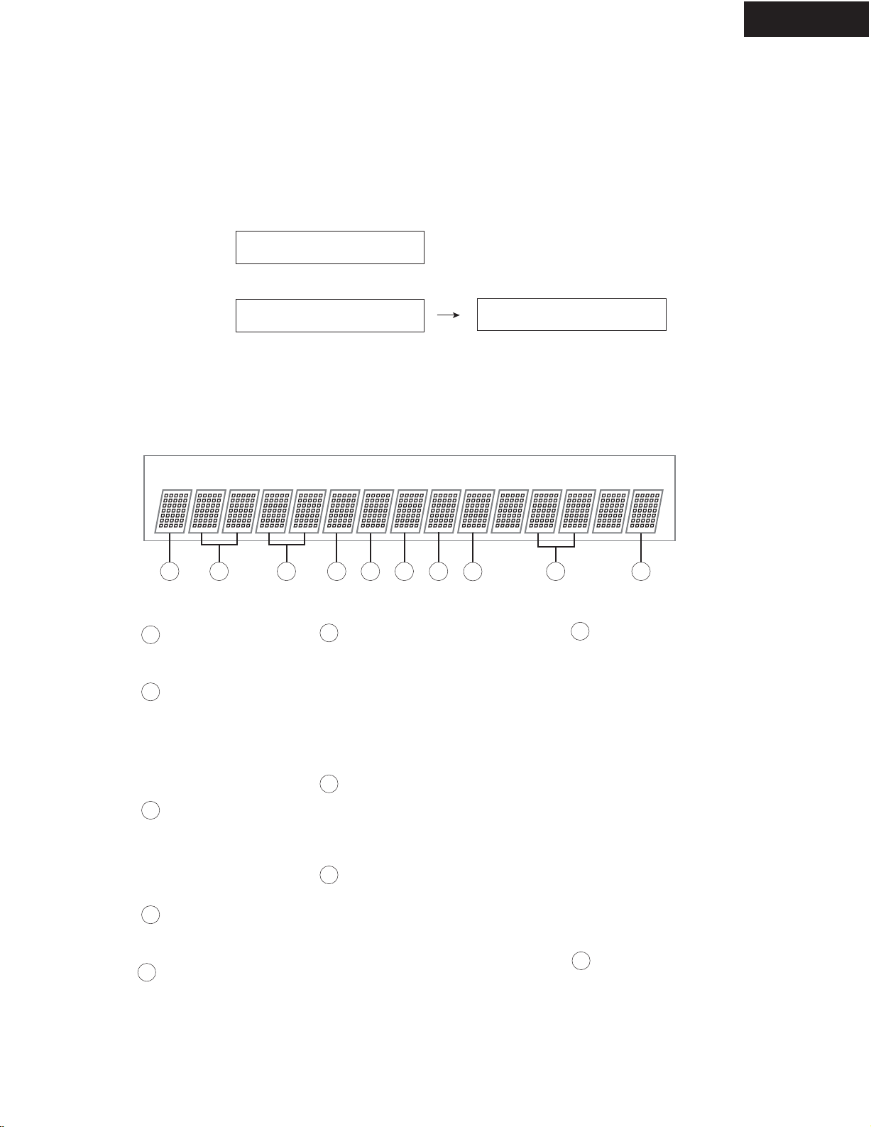
STANDBY/ON
SPEAKERSBA
PHONES
SERVICE MANUAL
AV RECEIVER
MODEL HT-R820THX
STANDBY
LISTENING
MODE
VIDEO 1
DISPLAY TUNING MODEDIGITAL INPUT
VIDEO
VIDEO 2
3
VCR
MEMORY
TAPE TUNER
CLEAR
TONE
THX
HT-R820THX
Ref. No. 3838
102004
ON STANDBY
T
V
INPUT
I
V1 V2 V3
+
123
TV CH
DVD MULTI CH
-
456
CD
TAPE TUNER
789
V VOL
T
CLEAR
+
10 0
--/---
TUNER/
TONE
TAPE
_
AMP
+
REMOTE MODE
CDR
DVD
CD MD
TV VCR
CABLE
OPEN/CLOSE
+
CH
DISC
-
REC
SURR
TEST TONE
M
P
O
T
E
R
E
T
U
SP A SP B
SUBTITLEAUDIO
ALL ST
DIRECT
CH SEL
VIDEO OFF
OR-EQ
RC-571M
SAT
M
U
N
E
E
N
U
ENTER
VOL
E
X
D
I
I
T
U
G
P
U
T
R
E
N
S
MUTING
RANDOM
ANGLE
LAST M
THX
STEREO
MEMORYA-BREPEAT
SEARCH
DSP
DSP
LEVEL -LEVEL +
Re-EQ
L NIGHT
TUNING
ENTER
C D
MASTER VOLUME
PRESET
RETURNSETUP
INPUT
VIDEO 3
VIDEO
S VIDEO
AUDIO
LR
DIMMER SLEEP
TV
INPUT
PREV
CH
DISPLAY
HT-R820THX
Black model
120V AC, 60HzBMDC
SAFETY-RELATED COMPONENT
WARNING!!
COMPONENTS IDENTIFIED BY MARK ON THE
SCHEMATIC DIAGRAM AND IN THE PARTS LIST ARE
CRITICAL FOR RISK OF FIRE AND ELECTRIC SHOCK.
REPLACE THESE COMPONENTS WITH ONKYO
PARTS WHOSE PART NUMBERS APPEAR AS SHOWN
IN THIS MANUAL.
MAKE LEAKAGE-CURRENT OR RESISTANCE
MEASUREMENTS TO DETERMINE THAT EXPOSED
PARTS ARE ACCEPTABLY INSULATED FROM THE
SUPPLY CIRCUIT BEFORE RETURNING THE
APPLIANCE TO THE CUSTOMER.
RC-571M
Page 2
SPECIFICATIONS
HT-R820THX
Amplifier Section
Power output:
All channels:
Dynamic power:
THD (total harmonic
distortion):
Damping factor:
Input sensitivity and
impedance:
Output level and impedance:
Frequency response:
Tone control:
S/N ratio (Direct mode):
Speaker impedance:
Video Section
Input sensitivity, output
level and impedance:
Component video
frequency response:
Tuner Section
FM
Tuning frequency range:
Usable sensitivity:
S/N ratio:
THD:
FM stereo separation:
130 W (8 , 20 Hz-20 kHz, FTC)
2 x 260 W (3 , front)
2 x 200 W (4 , front)
2 x 150 W (8 , front)
0.08% (rated power)
60 (front, 1 kHz, 8 )
200 mV/47 k (LINE)
200 mV/470 (REC OUT)
10 Hz-100 kHz/+1 dB,
-3 dB (Direct mode)
±12 dB, 50 Hz (BASS)
±12 dB, 20,000 Hz (TREBLE)
100 dB (CD, IHF-A)
8 ~
1.0 Vp-p/75
(component and S-Video Y)
0.7 Vp-p/75
(component PB/CB, PR/CR)
0.28 Vp-p/75 (S-Video C)
1.0 Vp-p/75 (composite)
5 Hz-50 MHz
87.5-107.9 MHz
FM STEREO 17.2 dBf, 2.0 µV (75 IHF)
FM MONO 11.2 dBf, 1.0 µV (75 IHF)
FM STEREO 70 dB (IHF-A)
FM MONO 76 dB (IHF-A)
FM STEREO 0.3% (1 kHz)
FM MONO 0.2% (1 kHz)
45 dB at 1 kHz
General
Power supply:
Power consumption:
Standby power consumption:
Dimensions
(W x H x D):
Weight:
Video Inputs
Component video inputs:
S-Video inputs:
Video inputs:
Video Outputs
Component video outputs:
S-Video outputs:
Video outputs:
Audio Inputs
Digital inputs:
Analog inputs:
Multichannel analog inputs:
Audio Outputs
Analog outputs:
Subwoofer pre out:
Speaker outputs:
Phones:
Specifications and features are subject to change without notice.
AC 120 V, 60 Hz
6.6 A
2.5 W
17-1/8" x 5-7/8" x 14-13/16"
(435 x 150 x 376 mm)
22.5 lbs. (10.2 kg)
2 (DVD, Video 1/2/3)
4 (DVD, Video 1-3)
4 (DVD, Video 1-3)
1 (Component Video Out)
2 (Video 1 Out, Monitor Out)
2 (Video 1 Out, Monitor Out)
4 (Optical 1-3, Coaxial)
6 (CD, Tape, DVD, Video 1-3)
5.1 ch (Front L/R, Center, S
urround L/R, Subwoofer)
2 (Tape Out, Video 1 Out)
1
6+2
1
AM
Tuning frequency range:
Usable sensitivity:
S/N ratio:
THD:
530-1710 kHz
30 µV
40 dB
0.7%
Page 3
SERVICE PROCEDURES
1. Replacing the fuses
This symbol located near the fuse indicates that the
fuse used is show operating type, For continued protection against
fire hazard, replace with same type fuse, For fuse rating, refer to
the marking adjacent to the symbol.
Ce symbole indique que le fusible utilise est e lent.
Pour une protection permanente, n'utiliser que des fusibles de meme
type. Ce demier est indique la qu le present symbol est apposre.
REF NO. PART NO. DESCRIPTION
F6901, F6902
F6901, F6902
F6901 or, F6902 or
F901
F901 or
F903
F903 or
2. Safety-check out
After correcting the original service problem perform the
following safety check before releasing the set to the customer
Connect the insulating-resistance tester between the plug of
power supply cord and terminal GND on the back panel.
Specifications: More than 10Mohm at 500V
252199
252100
252307
252198
252261
252164
252258
10A-UL
10A-EAK
10A-TL250V
8A-UL
8A-T/UL-ST2
5A-UL/T-237
5A-T/UL-ST2
REMARKS
5. Memory backup
The HT-R820THX uses a battery-less memory backup
system in order to retain radio presets and other settings
when it's unplugged or in the case of a power failure.
Although no batteries are required, the HT-R820THX
must be plugged into an AC outlet in order to charge the
backup system.
Once it has been charged, the HT-R820THX will retain
the settings for several weeks, although this depends on
the environment and will be shorter in humid climates.
6. Changing the AM band step
1. Necessary to change as follows.
R7003 Change to 10 kohms. Refer to <Fig-1>
R7004 Change to 10 kohms. Refer to <Fig-1>
2. To select.
Press and hold down the TUNER button , then press the
MEMORY button.
<Fig-1>
NADG-8230 (Pre-amplifier PC board)
Component side
25138230B
NCDG-8230
HT-R820THX
3. To initialize the unit
This device employs a microprocessor to perform various
functions and operations. If interference generated by an external
power supply, radio wave, or other electrical sauce results in accident
which causes the specified operations and functions to operate
abnormally.
To perform a result, please follow the procedure below.
1. Press and the hold down the VIDEO 1 button, then press the
STANDBY/ON button when the unit is Power On.
2. After "Clear" is displayed, the preset memory and each mode
stored in the memory, are initialized and will return to the
factory settings.
4. To check version of microprocessor
<Note>
Main microprocessor Q7008 only.
1. Press and the hold down the DISPLAY button , then press the
STANDBY/ON button when the unit is Power ON.
Version is displayed on FL display only for 3 seconds.
<ex.>
2. Press the STANDBY/ON button to Power Off.
Ver. 075 (04809a)
Q7008
Main microprocessor
R7003
GND
R7004
P7701
232RXD
232TXD
NC
FVCC
Page 4

OPERATION CHECK-1
DC VOLTAGE DETECTION PROTECTORS
<Note1>
In test mode " Test 4-20 " to " Test 4-31 ", DC voltage is outputted from DSP IC a pre-amplifier section, and it is inputted into a
power amplifier circuit.
Therefore an external input is unnecessary in check.
<Note2>
Don't connect speakers or any load.
Don't short speaker terminals.
1. Set the unit to test mode " Test-4-00 " .
1-1. Press and the hold down the CD button , then press the STANDBY/ON button when the unit is Power On.
HT-R820THX
1-2. Press the VIDEO 3 button, while the " Test - _ " is shown.
Unit will be in the state of " Test-4-00 ".
Test - _
blinks
Test - 4-00
2. Repeat and press SPEAKERS B to the " Test-4-20 " is shown.
Test - 4-20
3. Check that the " Protect OK " is shown and speaker relays are turn Off.
Protect OK
If a circuit is failure, the " Protect NG " is shown.
Protect NG
4. Check about the " Test 4-21 " to " Test 4-31 " one by one.
Refer to <Fig-1> about the operation method.
5. Press the STANDBY/ON to power Off. (Exit the test mode.)
<Fig-1>
Operation method
Press on " SPEAKER B " button ---> Next step
Press on " SPEAKER A " button ---> Retarn
Details of TEST MODE 4-20 to 4-31
Test - 4-20
Press
" SPEAKER A " button.
Press
" SPEAKER B " button.
Test - 4-21
Press
" SPEAKER A " button.
Press
" SPEAKER B " button.
Test - 4-22
Test - 4-31
MASTER VOLUME = MAX.
TEST MODE
4-20
4-21
4-22
4-23
4-24
4-25
4-26
4-27
4-28
4-29
4-30
4-31
DSP
output ch.
FL
FR
C
SL
SR
SB
FL
FR
C
SL
SR
SB
DSP
output voltage
+DC
- DC
+DC
+DC
- DC
+DC
- DC
+DC
- DC
+DC
- DC
+DC
Page 5

OPERATION CHECK-2
CURRENT DETECTION PROTECTORS
<Note1>
In test mode " Test 4-32 ", the pulse waveform is outputted from DSP IC on the pre-amplifier section, and it is inputted into
a power amplifier circuit. Refer to <Fig-1>.
Therefore an external input is unnecessary in check.
<Note2>
Don't connect speakers or any load.
Don't short speaker terminals.
Don't check two or more channels simultaneously.
1. Set the unit to test mode " Test-4-00 " .
1-1. Press and the hold down the CD button , then press the STANDBY/ON button when the unit is Power On.
HT-R820THX
1-2. Press the VIDEO 3 button, while the " Test - _ " is shown.
Unit will be in the state of " Test-4-00 ".
Test - _
blinks
Test - 4-00
2. Repeat and press SPEAKERS B to the " Test-4-32 " is shown.
Test - 4-32
3. Connect the road resistor 3 ohms to the speaker terminal.
4. Check that the " Protect " is not shown.
5. Connect the road resistor 1.5 ohms to the speaker terminal.
6. Check that the " Protect " is shown, and speaker relays are turn off.
Protect
7. Check about the FL, FR, C, SL, SR and SB channel one by one.
8. Press the STANDBY/ON to power Off. (Exit the test mode)
<Fig-1>
The output waveform from DSP IC in the test mode 4-32.
Details of TEST MODE 4-32
TEST MODE
4-32
DSP
output ch.
ALL
DSP
output voltage
Max.
2 ms
MASTER VOLUME = 54
2 ms
20 ms
Page 6
OPERATION CHECK-3
OUTPUT LEVEL & THERMAL DETECTION
<Regarding the power supply system of this unit>
Function
1. High-voltage mode
Usually, the power supply supplies high voltage to the power amplifier circuit when the relay (RL6901) is turned On.
2. Low-voltage mode
When as follows, a power supply changes to the state of supplying low voltage when the relay (RL6901) is turned Off.
(1) Excessive output signal is continuously outputted from power amplifier.
(2) Temperature of a heat sink over 80 degrees.
Purpose
1. The loss which power amplifier generates is decreased. As a result, the miniaturization of a heat sink is realized.
2. Corresponds to a safety standard.
HT-R820THX
Block diagram
POWER AMP.
THERMAL
SENSOR
R6380
Q6303
THERMAL
DETECTION
OUTPUT
LEVEL
DETECTION
SPEAKER
OUT
+B1
-B1
VOLH
2
HIGH
---> +/- 68.0 V
MODE
LOW
---> +/- 33.5 V
MODE
Q7008
MAIN
MICROPROCESSOR
RL6901
D6903
RL6902
SEC1H
23
D6904
Q6901
F6901
F6902
High
Low
Low
High
Necessity of operation check
May not notice the fuse (F6901, F6902) broken in the case of repair.
Because the power supply is continuing supplying voltage from the High side of SEC1 at high-voltage mode.
When a power supply Circuit changes to low voltage mode, amplifier does not operate.
Therefore, it is very important to check operation of this power supply system containing a fuse.
<Procedure>
<Note>
Don't connect speakers or any load.
Don't short speaker terminals.
(1) Set the unit is Multi channel input state.
(2) Set the master volume into the minimum.
(3) Apply sine wave signal to MULTI CHANNEL INPUT (FL+FR+C+SL) terminals.
(4) Connect an oscilloscope to speaker terminal of FL channel.
(5) Adjust master volume so that the wave form of speaker output may become distortion about 5%.
SEC1
T901
MAIN TRANS.
PRI.
High-voltage
(6) Check that the RL6901 is turned off after about 5 seconds.
And the power supply changes to low-voltage mode.
Low-voltage
(7) Adjust the master volume so that output voltage may become half.
(8) Check that the RL6901 is turned On after 2 to 3 minutes.
And the power supply returns to high-voltage mode.
Page 7
OPERATION CHECK-4
OUTPUT LEVEL & THERMAL DETECTION
<Operation check of microprocessor by test mode>
The following is the procedure of checking detection operation of a microprocessor in false, by using test mode.
Output level detection
1. Set the unit to test mode " Test-3-3 "
1-1. Press and the hold down the CD button , then press the STANDBY/ON button when the unit is Power On.
HT-R820THX
Test - _
1-2. Press the VIDEO 2 button, while the " Test - _ " is shown.
Unit will be in the state of " Test-3-00 ".
Test - 3-00
1-3. Repeat and press SPEAKERS B button to the " Test-3-3 " is shown.
Test - 3-03
2. Apply signal (sine wave 1kHz, -1.5dBV) to MULTI CHANNEL (FL, FR, SL, SR, C) terminal, each channel.
3. Check that FM STEREO indicator is shown.
FM STEREO
FM STEREO
Test - 3-03
4. Press the STANDBY/ON button to power Off. (Exit from the test mode.)
Thermal detection
1. Set the unit to test mode " Test-3-3 "
Refer to the clause of " Output level detection ".
2. Connect the resistor 1.8kohms /1W between " HT2 " and " COM " terminals of P6301.
P6301
1.8 kohms
1W
TH1
TH2
COM
TH1
COM
TH2
P6301
U16
NAAF-8245
POWER AMPLIFIER PC BOARD
3. Check that FM STEREO indicator is shown.
MEMORY
MEMORY
Test - 3-03
4. Press the STANDBY/ON button to power Off. (Exit the test mode.)
Front side
Page 8
OPERATION CHECK-5
DSP DEBUG MODE
<Regarding the DSP debug mode>
TIn this test mode, the check with normal communication of a microcomputer and the data of DSP and DIR is possible.
This information is a help to find the cause of failure.
How to go in DSP debug mode?
1. Press and hold down the DISPLAY button, then press the STANDBY button when the unit is power On.
HT-R820THX
<Ex.>
Ver. 075 (04809a)
2. Press the DISPLAY button, while the "Version 02415A" is shown.
DSP Debug Mode
How to Exit
Press STANDBY/ON button to power Off.
<Explanation of each parameter>
Details of display
1 42 5 6 97 103
DIR MEMORY/DOWNLOAD
AUTOBOOT DSP AB CODE
1
UNLOCK
E = UNLOCK
= LOCK
Digital Selecter
2
D = DIGITAL
A = ANALOG
1 = COAX
2 = OPT1
3 = OPT2
4 = Others
3
Sampling Frequency
96 = 96kHz
48 = 48kHz
44 = 44kHz
32 = 32kHz
= Not detect
Pre Emphasis
4
K = OFF
e = ON
DIR Status
5
0 = PCM/ANALOG
2 = DTS CD
5 = DD/DTS/AAC
6
0 = DTS NEO:6
1 = DD PCM
2 = DTS-ES
3 = AAC
4 = SIG
5 = COS
6 = DTS96/24
7 = PL2FS
77
AUTOBOOT DSP C CODE
0 = PL2X (Except DTS 96/24)
1 = DTS 96/24
2 = NEO6
3 = T-D
8
AUTOBOOT Status
O = Autoboot is complete
X = Autoboot is going on
E1A48K010o 23 o
8
DSP
9
10
DSP Detect Format
[IEC61937]
00 = Null
01 = Dolby Digital
03 = Pause
04 = MPEG1 L1
05 = MPEG1 L23/MPEG2 w/o
06 = MPEG2 w/o
07 = MPEG2 AAC
0B = DTS1
0C = DTS2
0D = DTS3
1B = MPEG2 AAC1
1C = MPEG2 AAC2
[Except IEC61937]
20: Silent
21: DTS LD
22: DTS CD
23: PCM
DSP Decode
0 = Decode OK
X = Decode NG
- = Analog in
Page 9

HT-R820THX
EXPLODED VIEWS-1
A402
P901
A031
U11
F6902
F6901
U19
F903
A003
F901
A025
A401
A003
Refer to
"EXPLODED
VIEWS-2"
A003
U12
A003
U16
U06
U26
P306B
70+/-5mm
U07
A003
U27
U21
A003
A033
U14
A037
U09
P101
A003
A003
U01
A003
A052
x6
P7503
P7502
A003
A003
A050
A705
U05
A001
A003
U18
T901
P800
x 10
U20
A017
U10
A015
A017
A011
A003
A054
A056
A003
U03
U04
x 4
x 8
x 4
A003
U02
A003
A409
A003
A062
A402
A407
A060
HT-R820THX
Page 10

EXPLODED VIEWS-2
POWER TRANSIST OR SECTION
Q6050
HT-R820THX
A034
L=300+/-5mm
Q6060
Q6051
Q6061
Q6052
Q6062
Q6053
Q6063
A039
x12
Q6054
Q6064
Q6050A
x12
Q6065
Q6055
HT-R820THX
Page 11
A
BCDEFGH
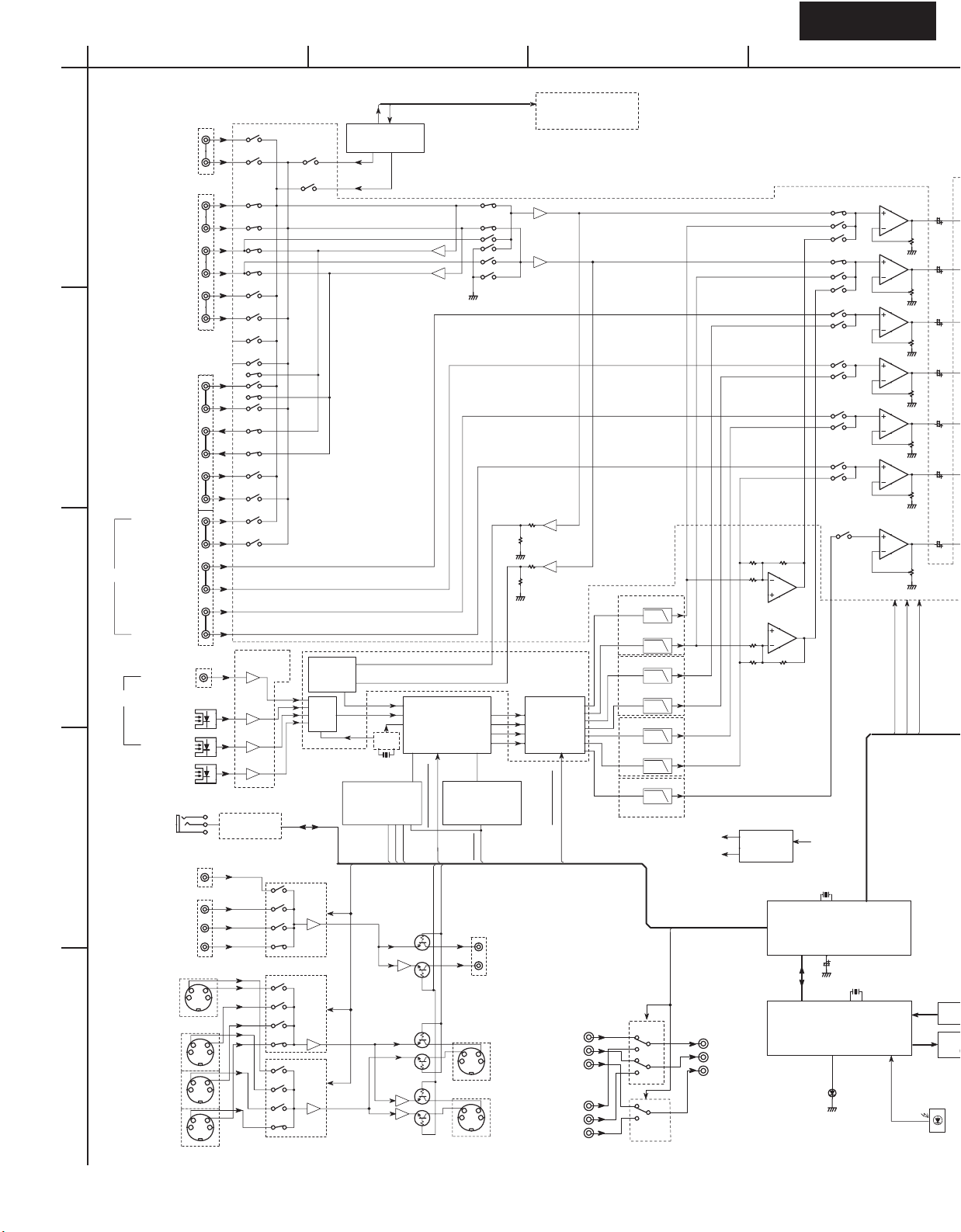
BLOCK DIAGRAM
VIDEO3
1
CD
TAPE OUT
TAPE IN
VIDEO-1 OUT
DVD
DIGITAL IN
VIDEO
S-VIDEO
VIDEO 2 IN
VIDEO 1 IN
VIDEO-2 IN
VIDEO-1 IN
FRONT
SURR.
CENTER
SUB WOOFER
COAXIAL
OPTICAL 1
OPTICAL 2
OPTICAL 3
RI
VIDEO3
VIDEO2 IN
VIDEO1 IN
DVD
VIDEO 3
DVD
L
R
L
R
YC
YC
YC
YC
2
3
4
5
11
12
7
8
93
94
9
10
11
12
13
14
95
96
15
16
24
25
27
28
26
30
Q281
74HCU04
RI
INTERFACE
VIDEO SELECTOR
LA7956
Q203
6dB
LA7956
Q213
6dB
LA7956
Q212
6dB
2CH A/D
96/24
DIR
FM/AM TUNER
UNIT
3
4
Q301
BD3817KS
SELECTOR
VOLUME
TONE CONTROL
OSC.
12.288MHZ
Q702
MX29LV040
FLASH
MEMORY
A17
CTLA/B
1
1
Q701
CS494003CQ-Z
DSP
A16
A15
RST.CS.INTREQ/CL/DA/SCDO
VMUT1
VMUT2
MUTE
Q202
0dB
Q201
MUTE
Q211
Q
Q210
Q207
0dB
0dB
Q208
Q7301
IC42S16100
16M SDRAM
(520 ONLY)
ROM/RAM
VIDEO OUT
MONITOR OUT
VIDEO 1
S-VIDEO
YC
MONITOR
OUT
YC
VIDEO 1
MAIN MICRO
PROCESSOR
1
1
-6dB
1
-6dB
1
Q800
AK4588VQ
96/24
8CH D/A
RST.CS/CL/DA/CDTO/INT1.2.
DVD IN
CB
CR
CY
VIDEO
1/2/3 IN
CB
CR
Y
Q804
L
50KLPF
R
50KLPF
Q802
SL
50KLPF
SR
50KLPF
Q803
C
50KLPF
SW
50KLPF
SB
50KLPF
Q801
COMPONENT
VIDEO
RL242
RL241
+6dB
+6dB
+6dB
+6dB
+6dB
+6dB
+6dB
3938414240
DSP
CPNT
44
POWER SUPPLY
+2.5V
+3.3V
OUT
CB
CR
Y
91
+4.5dB
-6dB
Q302(1/2)
Q302(1/2)
-6dB
+4.5dB
Q7004
BA33C25
12.5MHZ
MAIN MICROPROCESSOR
MPD784225GC
SUB MICROPROCESSOR
MPD780232GC
92
43
+5VDSP
Q7008
BACK UP
Q7502
INPUT GAIN
INPUT GAIN
INPUT GAIN
INPUT GAIN
INPUT GAIN
INPUT GAIN
INPUT GAIN
5MHZ
STANDBY
D7507
0/6dB
0/6dB
0/6dB
0/6dB
0/6dB
0/6dB
0/6DB
SELDA
SELCL
79 78
81 80
53 54
55 56
57 58
48 49
51 52
SELMUT
OPERATION KEY
U7501
REMOTE
SENSOR
MASTER
VOLUME
0,,-103DB
FL DISPLAY
Q7501
Page 12
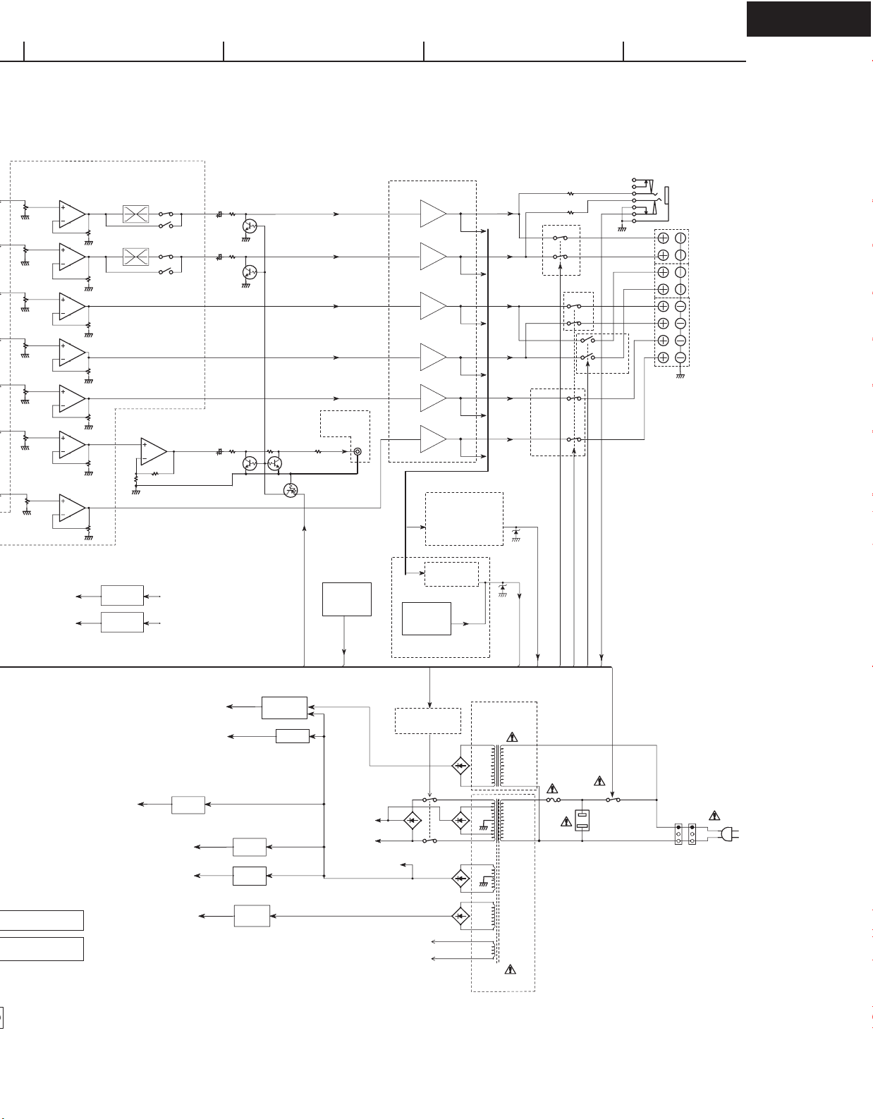
MASTER
VOLUME
0,,-103DB
BD3817KS,
OP AMP.
OUTPUT GAIN
0-18dB
OUTPUT GAIN
0-18dB
OUTPUT GAIN
0-18dB
OUTPUT GAIN
0-18dB
OUTPUT GAIN
0-18dB
OUTPUT GAIN
0-18dB
+7V
-7V
BASS/TREBLE
BASS/TREBLE
15dB
61
Q305
63
POWER SUPPLY
Q321
78L07
Q322
79L07
+12VAF
-12VAF
68
Q307
70
Q308
64
65
66
Q312 Q313
MUTING
MUTING
MUTING
SWPO
Q306
AMUT
SUBWOOFER
PREOUT
R6831
THERMAL
SENSOR
PROTHERM
POWER AMPLIFIER
+27dB
+27dB
+27dB
+27dB
+27dB
+27dB
DC VOLTAGE
DETECTOR &
OVER CURRENT
DETECTOR
Q6701~6703
VOLTAGE
SENSOR
R6830
THERMAL
SENSOR
FOR SEC1
VOLTAGE CONTROL
D6704
D6703
VOLH
RL6800
RL6803
PRO
RL6804
SPF
SPCS
SPB
RL6801
HPDET
PHONES
L
FRONT SPEAKERS-A
R
L
FRONT SPEAKERS-B
R
L
SURROUND SPEAKER
R
CENTER SPEAKER
SURROUND BACK SPEAKER
HT-R820THXHT-R820THX
OPERATION KEY
FL DISPLAY
Q7501
VIDEO
SECTION
MICROPROCESSOR
SUB
MICROPROCESSOR
+12V
Q6405
78M12
PRE-AMPLIFIER
SECTION
DSP SECTION
-12VAF
-12VAF
+5VDSP
+5.6V
-VP
Q6402
78M12
Q6403
79M12
Q6406
78M05
Q6931
NJM78M56A
Q9501
POWER
AMP.
+B1
-B1
SEC1 VOLTAGE
RL6901
RL6902
+B2
FL TUBE
SEC1H
CONTROL
D6904D6903
D9602
D9513
FLAC
FLAC
D921
-924
+B1H
+B1L
-9505
SUB
TRANSFORMER
T902
SEC1
SEC2
SEC3
T901
MAIN
TRANSFORMER
RL901
P902
AC OUTLET
POWER
AC IN
Page 13

HT-R820THX HT-R820THX
A
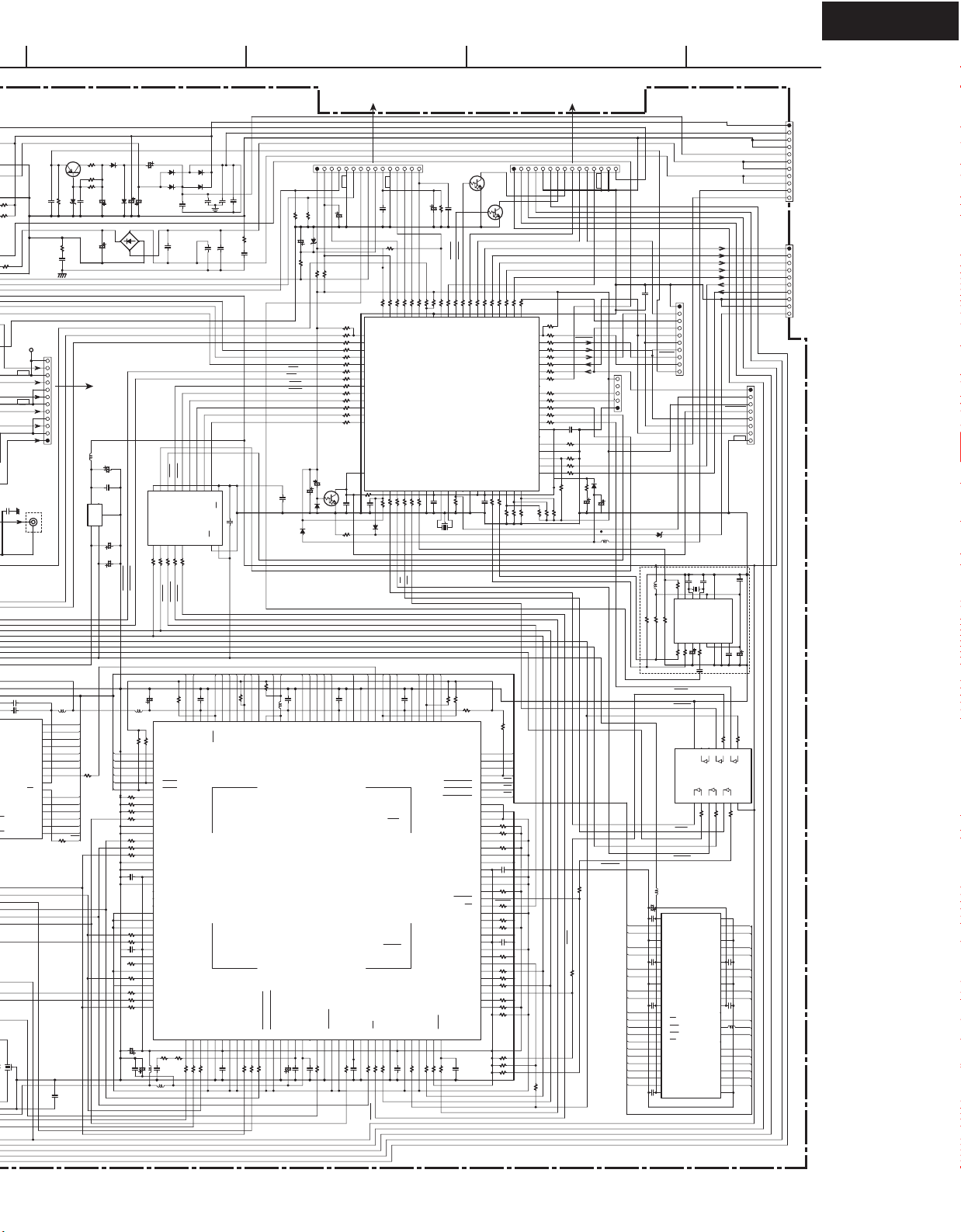
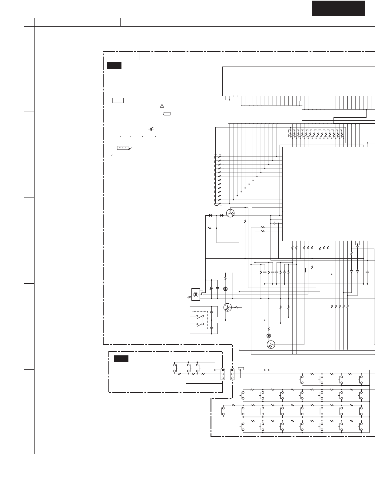
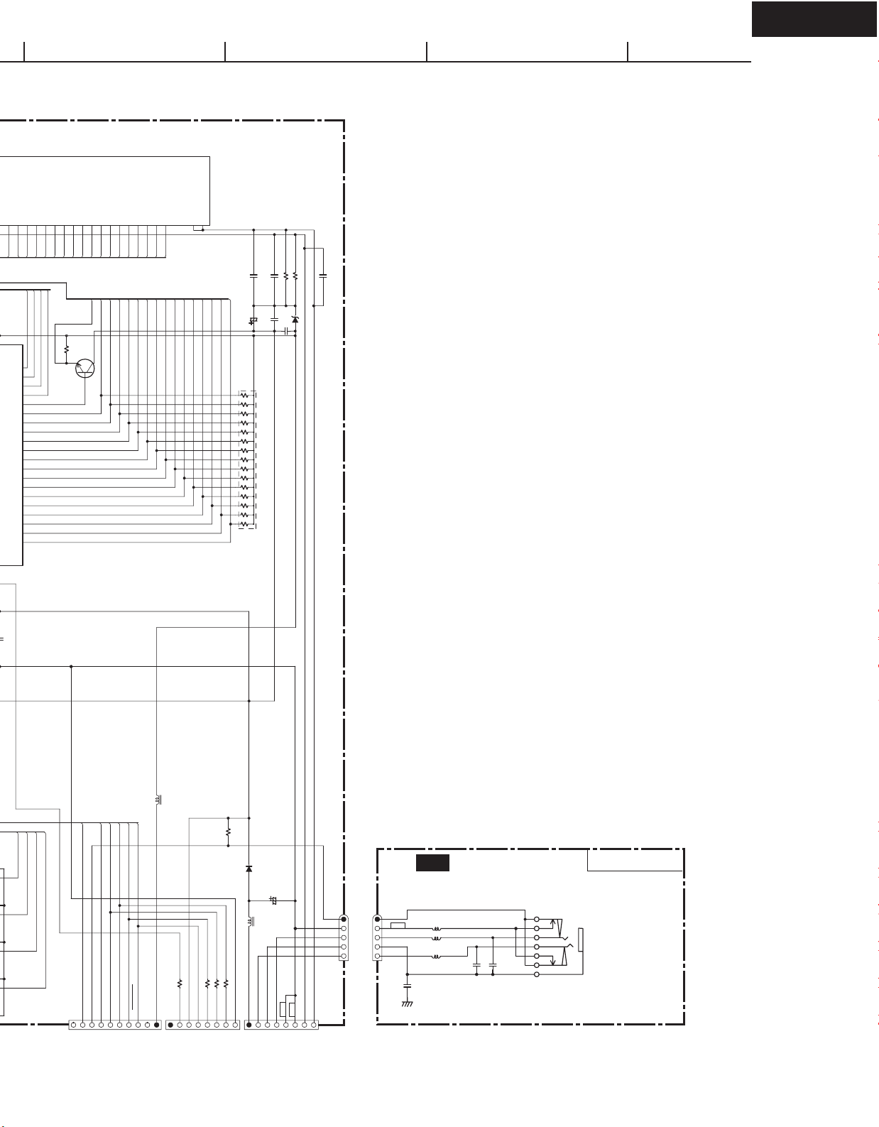
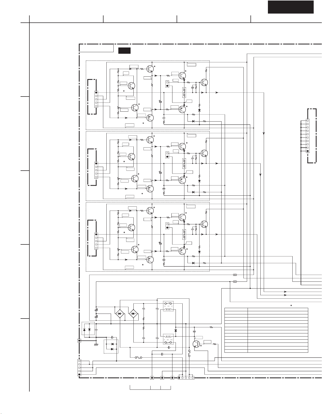
SCHEMATIC DIAGRAMS-1
PRE-AMPLIFIER SECTION
R300
P301
C308
C322
104Z
P302
NC
C323
104Z
P304
C325
104Z
P305
C326
104Z
DESCRIPTION
33K
330
R301
330
R302
330
330
R303
R304
330
103Z
330
R305
R306
NC
R307
NC
R310
330
330
R311
R312
330
330
R313
R314
330
330
R315
R316
330
330
R317
R318
330
330
R319
R320
330
R321
330
1
CD
TAPE-1 OUT
TAPE-1 IN
2
VIDEO-2 IN
VIDEO-1 OUT
VIDEO-1 IN
L
FRONT
R
L
DVD
SURR
R
CENTER
3
SUBWOOFER
<Notes>
NC=No mount of parts.
Refer to the following table about the parts displyed by mark " "
REF. NO.
R7003 000J
R7078 000J
R7079 10K
R7080 4.7K
R7178 NO
R7179 33K
R7180
4
5
BCDEFGH
TO NAETC-8234
P261A
R345
R346
47K
CDR SELDA
47K
R322
101K101K
R308
47K
000J
R323
CDL
TOR
Q316
R324
101J
470K
NC
101J
470K
R325
Q317
TIR V4L
R309
47K
000J
101J
C304C305 C303
R326
47K
101J
TIL TIL
R327
V3IR V3IL
47K
R328
47K
R329
V3IL V1IL OUT_RS
V2IR
47K
R332
101J
C310C311
47K
101J
R333
V2IL MLS
000J
R351
Q318
R334
101J
470K
C312
C313
C314C315C316C317C318C319C320C321 C300C301C302
NC
101J
470K
R335
Q319
R352
V1IR
000J
47K
R336
101J
47K
101J
R337
V1IL
DVDR
47K
R338
47K
DVDL DAC_L
R339
MRS RDSSCK
101J101J 101J101J
47K
R340
47K
R341
MLS
MSW
47K
101J
R342
47K
101J
R343
MC
47K
TOL
V1OR
V1OL
DAC_LS
DAC_RS
DAC_SW D5 A13
DAC_C DSPXTI SDWE
DAC_R
220/16
C843
C844
220/16
DAC_L
C856
10/16
NADG-8230
DMIXR
DMIXL
TOL
TOR
V1OL
V1OR
100
1
OUT1 98
OUT2 99
2
AGND14 97
AGND15
ROUTC1 95
INA24
INB15
INB26
INC17
INC28
IND19
IND210
INE111
INE212
INF113
INF214
ING115
ING2
INH117
INH2
INI1
INI220
INJ121
INJ222
AGND323
INDVDFR24
INDVDFL
INDVDC26
INDVDSR27
AGND431AGND535
AOUT132AOUT2
NJM4565M-D
OR MPC4570
C373
10/16
R361
10K
470K
R355
10K
C327
R409
330J
C328
330J
R356
10K
R410 470K
C374
10/16
NJM4565M-D
OR MPC4570G2
R401
R402
R403
R404
R405
6
5
8
C829
4
3
2
6
5
8
4
3
2
6
5
8
4
122J
3
2
101J
C838
101J
C840
6
5
8
122J
4
122J
3
2
C842
ROUTC2 96
AGND11
AGND22
INA13
INDVDSL28
INDVDCB29
INDVDSW
30
NC134NC236
33
8
7
Q302
R362
10K
Q302
1
4
47K
47K
47K
47K
47K
R862
R879
2.2K
122J
R880
2.2K
821J
4.7K
101J
C830
R865
4.7K
101J
C832
R866
R883
2.2K
821J
122J
C831
R884
122J
C833
2.2K
821J
101J
C834
R869
101J
R870
C835
R887
2.2K
822J
123J
C836
R888
2.2K
C837
C824
4.7K
R873
4.7K
R874
R891
2.2K
821J
C839
R892
2.2K
C841
821J
101J
R877
4.7K
TUR
3
TUL
V4R
CDR +5VDSP
CDL
TIR
V3IR OUT_R
V2IR OUT_L
V2IL
V1IR OUT_C
16
18
19
DVDR
DVDL
25
MC
MRS RSPO
28
29
MSW MCCLK
30
ADCR+ PROTHERM
ADCL+
DMIXR
DMIXL
NJM4565M-D
7
Q801
+12VA D6 A14
-12VA
C850
1
10/16
Q801
DAC_SBL
NJM4565M-D
NJM4565M-D
C851
10/16
7
Q802
10/16
1
Q802
C852
NJM4565M-D
NJM4565M-D
C853
10/16
7
Q803
C854
10/16
1
Q803
NJM4565M-D
NJM4565M-D
C855
10/16
7
Q804
1
Q804
NJM4565M-D
AGND13 90
ROUTA1 91
ROUTA2 92
ROUTB1 93
ROUTB2 94
BD3817KS
Q301
INDSPC40
INDSPFL39
INDSPFR38
INDSPSR41
NC337
DAC_R
DAC_L
DAC_C
DAC_RS
R357
5
000J
R347
10K
6
R387
1.5K
R386
1.5K
2
R358
3
000J
DAC_R
DAC_SW
R854 100K
4.7K
R831
2.2K
D801 D805
R832
2.2K
C820
R833
4.7K
R834
4.7K
C821
R835
2.2K
R836
2.2K
C822
R837
4.7K
4.7K
R838
4.7K
4.7K
C823
R839
2.2K
R840
2.2K
821J
R841
4.7K
R842
4.7K
C825
R843
2.2K
R844
2.2K
C826
R845
4.7K
VCC 89
INDSPSL42
DAC_LS
DAC_SBL
R359
390
R360
390
R348
10K
100K
R855
D806
D802
330
R814
RX1
NC8 88
INDSPCB43
DAC_SW
R852
C847
R826
C805
104Z
C808
104Z
330
R813
RX2
VEE 87
GOUTSL 53
GOUTSB 51
INDSPSW44
15K
10/16
56
C800
330J
C814
330J
PRE-AMPLIFIER PC BOARD
U01
SELCK
DATA 85
AGND12 86
VINFR
GOUTFL 79
VINFL 78
VINCB 52
AGND646
NC445
CL 84
80
NC5
47
C368
10/16
SELMUT
MUTE 83
THGND 82
AGND1177
TNF1 76
TNF2 75
BNFA1 74
BNFB1 73
BNFA2 72
BNFB2 71
OUTFR 70
NC7 69
OUTFL 68
AGND1067
OUTC 66
OUTSR 65
OUTSL 64
OUTCB 63
AGND9 62
OUTSW 61
NC6 60
AGND8 59
VINC 58
GOUTC 57
VINSR 56
GOUTSR55
VINSL 54
VINSW
GOUTSW48
49
GOUTFR 81
AGND7
50
104Z
104Z
10/16
C346
80
79
78
C345
C370 472J
C369
OUT_LS OUT_L
OUR_LB
OUT_SW
C347
C348
C363
53
52
51
C364
10/16
C376
C381
C372
10/16
10/16
10/16
10/16
C371
100/16
C341
C344
C343
C342
472J
104J
104J
R353
4.7K
104J
104J
R354
4.7K
NC
Q320
RN2402
R349
OR KRA102S
ADCL+
220K
C375
474K
R350
220K
C377
474K
Q323
RN2402
OR KRA102S
ADCR+
15K
R853
C846
10/16
R825
56
41
NC3 40
42
43
NC544
ROUT245
NC646
LOUT147
NC748
ROUT149
NC850
C804
LIN51
2.2/50
RIN52
VCOM53
VREFH54 XTI 7
AVDD55
AVSS56
RX057
58
59
60
C818
RX261
NC
330J
C817
R812
RX3
C809
330/6.3
330
224K
224K
39
LOUT3
NC10
62
R811
C378
C379
NC2 38
ROUT4 37
41
ROUT3
42
NC4
LOUT243
58
59
60
PVSS64
RX363
R810
330
TX
10/16
C349
T1RECMUT
V1RECMUT
1K
NC
R847NCR848
R824
R846
NC1 36
DZF1 34
LOUT4 35
AK4588VQ
NC9
RX1
TEST1
PVDD66
R65
RX467
12K
104Z
C811
R809 4.7
R367
CODECPD
1K
R808
MASTER 32
DZF2/OVF 33
Q800
RX569
TEST268
C816
100/6.3
Q321
78L07
+7V
IO
G
C359
10/16
Q322
79L07
-7V -12VA
IO
G
C362
10/16
100/16
C390
101J
C391
101J
C392
101J
C393
101J
C394
101J
2
Q305
1
3
4
NJM4565M
OR MPC4570
C351
330J
3.9K
1.8K
R369
R370
R383
10K
6
R368
47K
Q305
C350
221J
56
R823
RX773 SDTI1 28
5
56
R82256R821
SDTI2 27
SDTI3 26
CDTO 20
LRCK1 19
BICK1 18
TVDD 3
BOUT 2
INT1 1
DAUX275
I2C74
8
+12VA
NJM4565M
OR MPC4570
CODECCS
1K
1K
R805
R806
23
24
CSN
SDTI4 25
DAUX1
MCKO1 10
MCKO2 9
MCLK77
TX078
VIN76
7
DSPDA_33
22
CDTI/SDA
SDTO1 17
LRCK216
BICK2 15
SDTO2 14
VOUT 13
UOUT 12
COUT 11
TEST3 8
DVSS
DVDD 4
TX179
1K
1K
1K
NC
R829
56
R827
R800
PDN 31
XTL0 30
XTL1 29
CAD070
CAD172
RX671
Q6402
+12VA
G
C6404
C366
104Z
10/16
Q6403 79M12
O
G
C6406
10/16
C367
104Z
C353
OUT_R LPO
OUT_RS
C355
C356
OUT_LS CPO MCMDA
OUT_C
C357
C395
101J
47/16
DSPCLK_33
DACDA4
DACDA3
DACDA2 INT1
DACDA1 FINT
1K
R803
2.2K
R828
21
R804
20
R802
19
R801
18
CCLK/SCL
R849
R819
R820
R816
L802
LM182
R818
330
C813
XTO 6
5
3
C806
2
104Z
1
INT080
C807
100/6.3
C722
104Z
L800
022M
C6410
10/16
C6412
10/16
C354
47/16
C380
C358
+12VVD
47/16
R373
R374 1.2K
R375 1.2K
56
56
56
56
560
56
L803
022M
330/6.3
C815
104Z
022M
3VINT1
R817
56
R331
1.2K
R344
R396
R397
R363
R389
1.2K
R376
270
Q312
RN1441
L801
TX
RX1
RX2
RX3
1.2K
Q6405
R330
1.2K
3VDSI
R384
220K
3VINT1
O
Q6406
O
R388
100
3VINT0
3VINT0
R807
G
G
78M12
C6411
223Z
56
1/2W
10
IO
C6403
223Z
R6403
1/2W
33
I
I
C6409
223Z
I
C360
7805
Q307
RN1441
474K
C6405
223Z
Q308
RN1441
Q309
NC
Q310
NC
Q311
NC
Q314
NC
Q313
RN1441
Q306
RN2402
OR KRA102S
+2.5
+3.3V
+3.3V
104Z
C781
-22V
R6407
1W
3.3
Q6407
NC
R6408
NC
R6406
NC
R6405
NC
Q6408
NC
R6411
1/2W
1.0
22K
R377
22K
R378
GND
RPO
22K
R379
GND
LSPO MPURST
22K
R380
SBO
22K
R381
22K
R390
SUBWOOFER
C352
104Z
PREOUT
R385
100
SWPO
22K
222J
C365
R382
C361
224K
C751
C752
A3 A4
A317 A4 16
A2 A5
A218
A1 A6
A119
A0 A7
A020
D0 A12 A0 D2
DQ021
D1 A15 A1 D1
DQ122
D2 A16 A2 D0
DQ223
MX29LV040
VSS
A18/VPP 9
24
D3
DQ325
D4 CAS OE
DQ426
D5 A17 WE
D7 A13
CS A8
A10 A9
OE A11
DALRCK
DACBCK
ADSDO
DIRLRCK
DIRBCK
SAI_SDOUT
DIRMCKO
OMCK
+5VDSP
DACDA4
DACDA3
L783
220K
8
VCC
Q703
TC7WU04FU
1
WE/A18
DQ527
DQ628
DQ729
CE
30
A1031
OE
32
L781
L782
LM182
LM182
63725
X781
R781 1M
GND4
R6402
78M12
Page 14
TO TUNER UNIT
+22V
Q9501
2SA1015-GR
KTA1266-GR
-22V
NC
R6405
C352
104Z
1W
NC
1/2W
SWPO
R781 1M
100K
R9509
223Z
C9512
D9508
UDZS27D
R6421
4.7
C6401
104J
P6403
P406
GND
RPO
GND
LSPO MPURST
SBO
P306
SUBWOOFER
PREOUT
P351
AMUT
104
022M
104Z
L751
A5 15
A6 14
A7 13
A12 12
Q702
A15 11
A16 10
MX29LV040
A18/VPP 9
VCC 8
7
WE/A18
A17 6
A14 5
A13 4
A8 3
A9 2
A11 1
22
WE
R762
+5VDSP
X781
CSTCV12.2MTJ0C4
C721
104Z
R9506
22(1/2W)
D9507
R9507
15K
R9508
15K
C9511
223Z
C9508
4700/16
TO NAAF-8235
C7015
022M
L7002
NCH-1471
47/16
C7014
104Z
NC2VI
1
G
3
4
Q7004 BA33C25FP
2.5V53.3V
47/16
C7011
C7012
47/16
A18
R763
22
SAI_SDOUT
DIRLRCK
DIRBCK
DACBCK
DIRBCK
DIRLRCK
DALRCK
-VP
C9505
D9506
C9510
220/63
D9513 D2SB80A
CODECPD
A3 SDWE
RAS
3.3K
47
47
47
47
47
47
104Z
C714
R730
R731
104Z
C715
R732
R733
R734
R735
R736
47/16
C703
C702
104Z
CS_VDD
DIRLRCK
DIRBCK
D9502-9505:
D9505
C9507
220/35
2200/35
C9506
470/35
DSPCLK
A8 9
GND10
Q7002
TC74VHC541FT
Y712
Y8
11
R7067
R7068
220
220
CODECCS
DSPDA_33
DSPCLK_33
1/50
C713
CS_SDVDD
220M
L703
R7312
R7311
73
74
75
76
77
SDRAS
78
SDCAS
79
SDATAN3,GPIO27
R723
80
SDATAN2,GPIO26
R724
81
SDATAN1,GPIO25
R725
82
SDATAN0,GPIO24
R726
83
NC4
84
NC3
85
LRCKN,GPIO23
R727
86
SCLKN,GPIO22
R728
87
LRCK1
R729
88
NC2
89
NC1
90
VDD1
VSS1
91
92
AUDATA7,XMT958B,GPIO31
93
AUDATA6,GPIO30
94
AUDATA5,GPIO29
95
HDATA7,GPIO7
96
HDATA6,GPIO6
97
HDATA5,GPIO5
47
98
SCLK1
47
99
MCLK
100
VDD2
101
VSS2
102
AUDATA4,GPIO28
47
103
HDATA4,GPIO4
104
SCLK0
47
105
106
47
107
47
108
47
C701 47/16
3K
R701
L702
022M
L701
022M
C9501
104J
DSPDA
A7 8
Y613
R7069
220
3VFCS
C706
C9503
104J
FCS
A6 7
Y514
R7070
220
3VDRES
NC
R7313
330
R700
680J
RL1N4003
D9503
D9502D9504
C9514
DRES
A3 4
A4 5
A5 6
Y217
Y316
Y415
R7072
220
3VSCS
A10
SDBA
C712
EXTA10
SD_ADDR10,
SD_BA,EXTA19
AUDATA0
AUDAUA1
109
110
R737 47
R73847R739
104J
C9513
104J
C9515 104
C9516 104
1
A1 2
A2 3
G1
C7010
104Z
G2
VCC20
Y118
19
A4A5A6A7A8
SDCS
104Z
SDCS
VSSSD1
VDDSD1
SD_ADDR5,EXTA5
SD_ADDR4,EXTA4
SD_ADDR1,EXTA173
SD_ADDR1,EXTA1
74
SD_ADDR2,EXTA2
75
SDADDR3,EXTA3
76
HDATA3,GPIO3
105
106
AUDATA3,XMT958A
107
AUDATA2
108
LRCK0
HDATA1,GPIO1
VDD3
VSS3
HDATA2,GPIO2
CMPCLK,FSCLKN2
111
112
113
114
115
47
104Z
C716
104J
C9502
R6422
4.7
C6421
104J
C7021
+5VDSP
R7315
R7314
A9
CKE
SD_ClL_IN
SD_CLK_EN
SD_ADDR8,EXTA8
SD_ADDR7,EXTA7
SD_ADDR6,EXTA6
CS494003CQZ
WR._DS,GPIO10
FLRCKN1
CMPDAT,FSDATAN2
CMPREQ,FLRCLKN2
HDATA0,GPIO0
116
117
118
119
120
47
47
R74147R742
R740
PLLCL
PLLDA
PLLSTB
TMUT
AMUT
PLLCL
PLLDA
PLLSTB
2.2K
220
220
220
470
R7038
R7037
R7035
R7034
R7036
1K
1K
R7066
R7063
R7065 1K
R7064 1K
INT0
FINT
INTDSP
C709
104Z
LDQM
VSSSD4
VDDSD4
SD_DATA6,EXTD6
SD_DATA5,EXTD5
36
35
34
33
4
3
2
1
FHS2,FSCDIO,FSCDOUT
HINBSY,GPIO8
SCDOUT,SCDIO
A1,GPIO12
VDD5
138
139
140
141
220
104Z
R748
C719
Q7006
KRC104S
OR RN1404
101J
3.3/50
C106
R104 100K
C103
VMUT1
VMUT2
PLLDI
220
220
1K
220
220
R7032
R7134
R7029
R7030
R7031
Q7008
4.7K
R7071
IC
C7008
104Z
X7001
CSTCV12.5MXJ
R7316
R7317
D4
D3
R722
10K
37383940414243444546474849
SD_DQM0
SD_DATA3,EXTD3
SD_DATA4,EXTD4
NVCS,GPIO14
NVOE,GPIO15
NVWE,GPIO16
FDAT0
TEST
FDAT1
DBCK
DBDA
FDAT2
FDBDA
FDAT3
VSS7
VDD7
FDAT4
FDAT5
FDBCK
FINTREQ
FCS
FDATA6
FHS1,_FRD,_FR/W
FHS0,_FWR,_FDS
VSS6
VDD6
FDAT7
GPIO21
FA0,FSCCLK
GPIO20
RESET
UHS,_CSOUT,GPIO17
SCCLK
142
143
144
220
R749
R751 220
101J
R750 3.3K
220
R7028
C720
220
R7027
C7009
36
35
34
33
32
31
30
29
28
27
26
25
24
23
22
21
20
19
18
17
16
15
14
13
12
11
10
9
8
7
6
5
4
3
2
1
R7076
Q7007
KRC104S
OR RN1404
220
R7026
104Z
R7077
3.3K
220
3.3K
3.3K
10K
220
10K
220
3.3K
3.3K
10K
DSPCLK_33
DSPDA_33
3VDSI
3VDRES
P101
SD
TUR
TMUT
STEREO
22K
R102 22K
R103
C109
D109
UDZS5.1B
330
22K
R109
22K
1/2W
R7138
R7839
AMUT
R7141
NC
R7041
NC
T1RECMUT HPMUT
V1RECMUT
SELMUT
SELCK
SELDA MCSDA
CODECPD MCRDY
CODECCS
FCS
DRES 232TXD
104Z
SDCLK
C711
L7302
LL241
VDDSD2
SD_CLK_OUT
SD_ADDR9,EXTA9
C7004
1/50
C7005
100/6.3
D7004
D7002
1SS352
A11
A12
A13
104Z
54555657585960616263646566676869707172
VSSSD2
SD_DATA9,EXTA12
SD_DATA8,EXTA11
SD_DATA10,EXTA13
R7042
NC
R7043
220
R7044
1K
R7045
1K
R7046
1K
R7047
220
R7048
220
R7049
1K
R7050
1K
R7051
1K
R7052
1K
R7053
220
KRC104S
RN1404
Q7001
C7006
R7033
47K
1SS352
A14
A15
C710
515253
VDDSD3
SD_DATA11,XETA14
SD_DATA12<XETA15
GND
GND
TUL
FMSIG
+12VA
RDSDET
C101
3.3/50
C104 101J
R107
NC
SD
STEREO
2.2K
220
R7039
R7040
40
41
42
43
44
45
46
47
48
49
50
MPD784225GC-267-8BT
51
52
53
54
55
56
57
58
59
60
R7060
47K
61626364656667686970717273747576777879
104Z
C7007
104Z
R7062 1K
D7003
220K
R7061
INT1
D7D6D5
A16
A17
A18
104Z
UDQM
50
NC5
VSSSD3
SD_DQM1
SD_DATA7,EXTD7
SD_DATA15,EXTA18
SD_DATA14,EXTA17
SD_DATA13,EXTA16
SD_DATA2,EXTD2
SD_DATA1,EXTD1
SD_DATA0,EXTD0
SDWE
Q701
FA1,FSCDIN
INTREQ
UHS1,GPIO19
UHS0.GPIO18
VSS5
SCDIN
SCS
FSCLKN1,STCCLK2
VSS4
VDD4
FSDATAN1
A0.GPIO13
CS,GPIO9
CLKSEL
CLKIN,XTALI
XTALO
PLLVDD
FILT1
FILT2
PLLVSS
RD,_R/W,GPIO11
121
122
123
124
125
126
127
128
129
130
131
132
133
134
135
136
137
47
220
220
47
47
TANTAL
C704
2.2M
DSPXTI
122J
C705
104Z
SAI_SDOUT
C717
R743
R744
104Z
C718
R745
3VSCS
R746
R747
TO NAETC-8243
P801
TX
RX2
RX1
+5VDSP
CTLB
CTLA
POWER
SPF SPF
SPCS SPCS
SEC1H SEC1H
SPB SPB
220
220
220
220
CNPT VOLH
HPIN
R7021
R7023
R7024
R7025
R7022
2.2K
21222324252627282930313233343536373839
20
19
18
17
16
15
14
13
12
11
10
9
8
7
6
5
4
3
2
1
INIT3
INIT2
INIT1
80
1K
1K
R7178*R7179
R7080
R7078
R7079
*
*
*
RDSSIG
RDSDATA
R7318
CS
R721
3.3K
R720
3.3K
R7193.3K
104Z
C708
R711
3VFCS
R710
R709
R708
104Z
C707
R707
R706
R705
R704
R703
R702
R712
3.3K
R714
R713
3.3K
R715
3.3K
R717
R7120
R7020
R7019
R7018
R7017
R7016
R7015
R7014
R7012
R7011
R7010
R7009
R7008
BAND
220
RX3
1K
C7003 104Z
R7005
R7180
*
VMUT1
NC
NC
220
220
220
*
VMUT2
220
220
82
82
82
82
82
R7003
R7002
R7001
NC
R7004
470K
CTLB
MCRST
MCCLK
MCMDA
232RXD
DSPCLK
DSPDA
DSI
1K
R7000
104F
C7001
L7001
3VINT
R718
220
RI
CTLA
2.2K
2.2K
100
NCH-1479
220
R716
CNPT
+12VVD
GND
104Z
C7020
RI
HPIN
MCRDY
MCSDA
MCMDA
MCCLK
MCRST
HPMUT
-VP
P7502B
TO RS232C
NC
P7701
VOLH
PROTECT
D7001
C7002
100/6.3
D7702
UDZS6.2B
NC
L181
NC
R184
47K
47K
47K
R185
R187
R186
RDSSIG
RDSDATA
NC
R182
RDSDET
DSI
3VINT
INTDSP
3VDSI
3VINT1
3VINT0
INT0
3VFINT
C7302
NC
C7303
NC
3VFINT
L7301
NC
C7307
NC
C7301
VCC01
NC
D0 A18
DQ02
D1
DQ13
GNDQ14
D2 A16
DQ25
D3 A15
DQ36
VCCQ17
D4 A14
DQ48
DQ59
GNDQ210
D6 A12
DQ611
D7 A11
DQ712
VCCQ213VCCQ3 38
LDQM
14
LDQM
WE15
CAS
CAS16
RAS CKE
17
RAS
SDCS
18
CS
SDBA A9
A1119
A10 A8
A1020
A0 A7
A021
A1 A6
A122
A2 A5
A223
A3 A4
A324
C7304
VCC1
25
NC
TO NADIS-8231
X181
C187
14
RST 15
XOUT
RDCL16
Q181
VREF3
RDDA2
RDS-ID/1
NC
R183
C181
NC
TC74HCT7007AF
NC
NC
Q7003
220
R7081
GNDQ4 47
VCCQ4
GNDQ3 41
UDQM 36
NC
Q7301
GND1 26
XIN 13
NC
MPXIN4
R181
C182
9
GND2 50
DQ15 49
DQ14 48
DQ13 46
DQ12 45
DQ11 43
DQ10 42
DQ9 40
DQ8 39
NC2 37
CLK 35
CKE 34
NC1 33
A9 32
A8 31
A7 30
A6 29
A5 28
A4 27
NC
C186
VDDA5 VDDD12
NC
NC
101112
220
R7082
VSSA6 VSSD11
FLOUT7MODE10
R7083 220
44
L7302
MCRDY
FVCC
MCSDA
C185
TEST 9
CIN8
C183
13
R7084 220
IC
GND
NC
C184
NC
220
R7085
12345678
14
+5VDSP
A17
C7305
NC
C7306
NC
UDQM
SDCLK
PROTHERM
NC
+22V
SEC1-1
SEC1-2
SEC3-1
SEC3-2
5.6S
POWER
PROTECT
GND
+13V
P412BFLASH
P410B
TO NAETC-8238
P411B
TO NAETC-8238
Page 15
HT-R820THX HT-R820THX
A
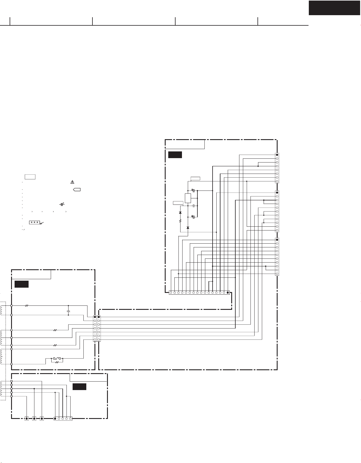
SCHEMATIC DIAGRAMS-2
DISPLAY SECTION
NADIS-8231
1
2
3
U02
NOTE
THE COMPONENTS IDENTIFIED BY MARK ARE CRITICAL FOR SAFETY
REPLACE ONLY WITH PART NUMBER SPECIFIED
VOLTAGE (MEASURED WITH VOLTMETER) IS DC VOLTAGE.(NO INPUT SIGNAL)
ALL PNP TRANSISTORS ARE EQUIVALENT TO 2SA1015-GR UNLESS OTHERWISE NOTED.
ALL NPN TRANSISTORS ARE EQUIVALENT TO 2SC1815-GR UNLESS OTHERWISE NOTED.
ALL DIODES ARE EQUIVALENT TO 1SS133 UNLESS OTHERWISE NOTED.
ELECTROLYTIC CAPACITORS ( ) ARE IN u F/WV.
ALL CAPACITORS ARE IN pF/50WV UNLESS OTHERWISE NOTED.
EX) 030- 3pF 330- 33pF 331- 330pF 333- 0.033uF
ALL RESISTORS ARE IN OHMS 1/4WATTS UNLESS OTHERWISE NOTED.
THE THICK LINES ON PC BOARD ARE THE PRINTING SIDE OF THE PARTS.
EX) PRINTING SIDE
CIRCUIT IS SUBJECT TO CHANGE FOR IMPROVEMENT.
IS DC VOLTAGE, AT NO INPUT SIGNAL.
<Notes>
NC=No mount of parts.
BCDEFGH
DISPLAY PC BOARD
R7582
NC
100K X 13
D7502
UDZ5.1B
R7505
220K
Q7504
RN2403
KRA103S
D7503
1SS352
F2F2NPNPP35
G[1]
P[35]
P[34]
P[33]
P[32]
SYSOUT
R7532
Q7501 HNA-16MM39T
P34
P33
P32
P31
P30
P29
P28
P27
P26
P25
P24
P23
P22
P21
P20
P19
P18
P17
P16
P15
P14
P13
P12
P11
P[6]
P[14]
P35/FIP29 49
Q7502
P2212
10K
R7515
P[7]
P[8]
P[13]
P[12]
P33/FIP27 51
P34/FIP28 50
P2311
P24/BUSY10
R7516 10K
P10P9P8P7P6P5P4P3P2
P[9]
P[10]
P[11]
P[12]
P[13]
P[14]
P[9]
P[8]
P[10]
P[11]
P[7]
P[6]
FIP22 56
FIP23 55
P31/FIP25 53
P32/FIP26 52
61:FIP19
IC5
P25SO19
P26/SI18
P27/SCK17 P30/FIP24 54
RESET6
10K
R999
5556575859
P[1]
G[2]
G[3]
G[4]
G[5]
G[6]
G[7]
G[8]
G[9]
G[11]
G[10]
R7581 100k X 14
NC
P[31]
P[30]
P[29]
P[28]
P[27]
P[26]
P[25]
P[24]
P[23]
C7507
10K
104Z
R7506 4.7K
R7507 4.7K
G[12]
27
22
21
G[13]
G[14]
P[22]
P46/FIP3840
P47/FIP3939
P50/FIP4038
P51/FIP4137
P52/FIP4236
P53/FIP4335
P54/FIP4434
P55/FIP4533
P56/FIP4632
P57/FIP4731
P60/FIP4830
P61/FIP4929
P62/FIP5028
P63/FIP51
P64/FIP5226
VDD025
AVDD24
VSS023
ANI220
4.7K
R7508
G[16]
G[15]
P[2]
P[3]
P[21]
P[20]
P[19]
P[18]
P[17]
43
P40/FIP32 46
P41/FIP33 45
P42/FIP34 44
41:P45/FIP374142:P44/FIP364243:P43/FIP35
MPD780232GC-096-8BT
22:ANI0
21:ANI1
ANI319
AVSS18
P01/INTP116
P02/TI17
POO/INTP015
1K
1K
R7509 4.7K
R7510
R7512 10K
R7511
P[4]
P[5]
P[16]
P[15]
P36/FIP30 48
P37/FIP31 47
P20/SCK314
P21/SO313
47k
R7504
FL TUBE
222324252627282930313233343536373839404142434445464748495051525354
P[17]
P[15]
P[16]
P[18]
P[5]
VDD2 59
FIP20 58
FIP21 57
61
VLOAD60
FIP18 62
FIP17 63
FIP16 64
FIP15 65
FIP14 66
FIP13 67
FIP12 68
FIP11 69
FIP10 70
FIP9 71
FIP8 72
FIP7 73
FIP6 74
FIP5 75
FIP4 76
FIP3 77
FIP2 78
FIP1 79
FIP0
80
VSS12
X13
X2
VDD11
4
X7501
CST5.00MGW
U7501
PIC-3704TH2
C7514
C7516
100/6.3
104Z
C7517
102J
R7513
2.7K
102J
102J
102J
R7520 2.7K
C7508 102J
2.7K
R7521
C7509
C7510
R7522 2.7K
10K
R7527
C7511
R7523
10K
R7526
NC
NC
D7504
R7514
NC
Q7507
NC
IRF
STBYLED
R7518
100K
1K
560
560
VAJ
VBJ
R7530
R7524 1K
R7517 1K
R7529
R7528
C7522 101J
C7523 102J
104Z
C7513
MASTER VOLUME
4
S7617
U03
SP A
S7616
SP B
S7501
S7615
STANDBY
OPERATION SWITCH
PC BOARD
R7617
2.2K
R7616
1.2K
NASW-8232
5
R7615
820
C7515
104Z
JL7501B
S7638
K3
SYSIN
K2
JL7501A
GND
KEY0
R7626
2.2K
S7627
S7637
S7647
MEMORY
CD
R7646
SET UP
2.2K
R7637 3.9K R7636 2.2K
FM MODE
S7626
S7636
S7646
R7625
1.2K
----
TUNER
RETURN
220
R7531
D7505
STANDBY
Q7506
RN1402
KRC102S
S7625
S7635
S7645
K1
R7624
820
DIGITAL
INPUT
TAPE
TUNING<
K0
S7614
S7624
S7634
S7644
R7613
560
TONE
R7623 560
DISPLAY
VIDEO3
TUNING>
S7613
S7623
S7633
S7643
TONE-
LISTEN
R7632
R7612
470
R7622
470
MODE>
VIDEO2
ENTER
SBMLDY
SBMDI
470R7633 560R7634 820R7635 1.2K
SBMDO
S7612
S7622
S7632
S7642
SBMCLK
SBMRST
R7611
330
TONE+
R7621
LISTEN
MODE<
R7631
VIDEO1
R7641
PRESET<
S7611
STEREO
330
CH
MULTI
S7621
330
DVD
S7631
ADJUST
330R7645 1.2K R7644 820 R7643 560 R7642 470
S7641
PRESET>
Page 16
P3P2P1
23
FL TUBE
16G
15G
14G
13G
12G
11G
10G9G8G7G6G5G4G3G2G1GNPNPF1
F1
10111213141516171819202122
123456789
P[18]
P[19]
P[20]
P[4]
61
VLOAD60
80
VDD11
X7501
CST5.00MGW
P[3]
P[21]
P[24]
P[25]
R7503
P[26]
G[1;16]
10K
P[27]
G[16]
P[28]
G[15]
P[29]
G[14]
P[30]
G[13]
P[22]
P[23]
P[2]
P[1]
Q7503
2SC2712
KTC3875
P[31]
G[12]
P[32]
G[11]
P[33]
G[10]
P[34]
G[9]
P[35]
G[8]
220
104Z
104Z
C7501
R7501 220
C7503
G[3]
G[7]
G[6]
G[5]
G[4]
G[2]
G[1]
C7502
33/50
473Z
C7504
C7505
473Z
R7580
10K X 15
NC
R7502
D7501
UDZ8.2B
C7506
104Z
CH
ADJUST
K0K1K2
K3
SYSIN
P7502A
TO NADG-8230
HPDET
SBMDI
SBMLDY
SBMDO
SBMCLK
SBMRST
L7505
-VP
NCH1477Z
P999
NC
220K
NC
R995
100K
R7519
D7507
1SS352
L7504
NC
NC
NC
R996
R998
R997
+5.6S
TO NAETC-8238
C7521
220/6.3
220K
NCH1477Z
HPR
HPE
U04
NAETC-8233
HEADPHONE TERMINAL
PC BOARD
HPDET
L7501
GND
L7502
HPL
HPE
L7503
HPR
JL7502A
FAC2
FAC1
HPL
GND
GND
P7503A
JL7502B
E7501
C7518
102J
C7519
102J
C7520
102J
P7501
PHONES
Page 17

HT-R820THX HT-R820THX
A
SCHEMATIC DIAGRAMS-3
DRIVER AMPLIFIER SECTION
NAAF-8235
DRIVER AMPLIFIER PC BOARD
1
2
U06
SL
R5003
1K
C5003
101K
R5043
D5003
MTZJ5.6B
BCDEFGH
2.2K
C5013
22/16
R5013
56K
R5103
100K
R5093
100K
-0.1V
R5023
330
-61V
C5023
10/50
Q5003
R5063
1.2K
R5113
1K
C5033
NC
-0.7V
R5053
4.7K
-61.6V
R5083
470
Q5053
Q5013
R5073
NC
C5103
10/100
C5043
100/16
R5133
18K
C5113
10/100
R5163
(1/4W)
150
1.0V
C5083
040D
R5173
150
(1/4W)
65.7V
Q5033
C5053
47/50
R5033
56K
Q5043
-65.7V
R5143
NC
65.1V
C5073
NC
0V
-1V
C5093
101J
-65.1V
R5183
10
(1/4W)
-B1
+B1
R5193
10
(1/4W)
-66.5V
NF
66.5V
B+
B-
P6003A
TO NAAF-8245
1.0V
C5084
040D
1.0V
C5085
040D
R5175
(1/4W)
R5164
150
65.7V
Q5034
C5054
47/50
R5034
56K
Q5044
-65.7V
R5165
150
65.7V
Q5035
C5055
47/50
R5035
56K
Q5045
-65.7V
(1/4W)
(1/4W)
R5144
NC
R5145
NC
R5184
10
(1/4W)
R5185
10
(1/4W)
R5194
10
(1/4W)
-66.5V
R5195
10
(1/4W)
-66.5V
-B1
+B1
-B1
+B1
NF
NF
66.5V
B+
B-
66.5V
B+
B-
P6004A
P6005A
TO NAAF-8245
TO NAAF-8245
NOTE
THE COMPONENTS IDENTIFIED BY MARK ARE CRITICAL FOR SAFETY
REPLACE ONLY WITH PART NUMBER SPECIFIED
VOLTAGE (MEASURED WITH VOLTMETER) IS DC VOLTAGE.(NO INPUT SIGNAL)
ALL PNP TRANSISTORS ARE EQUIVALENT TO 2SA1015-GR UNLESS OTHERWISE NOTED.
ALL NPN TRANSISTORS ARE EQUIVALENT TO 2SC1815-GR UNLESS OTHERWISE NOTED.
ALL DIODES ARE EQUIVALENT TO 1SS133 UNLESS OTHERWISE NOTED.
ELECTROLYTIC CAPACITORS ( ) ARE IN u F/WV.
ALL CAPACITORS ARE IN pF/50WV UNLESS OTHERWISE NOTED.
EX) 030- 3pF 330- 33pF 331- 330pF 333- 0.033uF
ALL RESISTORS ARE IN OHMS 1/4WATTS UNLESS OTHERWISE NOTED.
THE THICK LINES ON PC BOARD ARE THE PRINTING SIDE OF THE PARTS.
EX) PRINTING SIDE
CIRCUIT IS SUBJECT TO CHANGE FOR IMPROVEMENT.
IS DC VOLTAGE, AT NO INPUT SIGNAL.
SR
R5094
100K
3
R5004
C5014
22/16
1K
C5004
101K
2.2K
R5044
D5004
MTZJ5.6B
SB
4
C5015
R5005
22/16
1K
C5005
101K
2.2K
R5045
D5005
MTZJ5.6B
R5014
56K
R5104
100K
R5015
56K
R5105
100K
-0.1V
R5024
330
R5095
82K
[100K]
-0.1V
R5025
330
-61V
C5024
10/50
Q5005
-61V
C5025
10/50
Q5004
R5064
1.2K
R5065
1.2K
R5114
1K
C5034
NC
-0.7V
R5115
1K
C5035
NC
-0.7V
R5054
4.7K
Q5054
-61.6V
R5084
470
R5055
4.7K
-61.6V
R5085
470
Q5055
Q5014
Q5015
R5074
NC
R5075
NC
C5104
10/100
C5044
100/16
C5105
10/100
C5045
220 /16
R5134
18K
C5114
10/100
R5135
18K
C5115
10/100
65.1V
C5074
NC
0V
-1V
C5094
101J
-65.1V
R5174
150
(1/4W)
65.1V
C5075
NC
0V
-1V
C5095
101J
-65.1V
150
5
Page 18

P406AP407A
E
ESBECESLESRERELE
TO NADG-8230
P306A
<Notes>
NC=No mount of parts.
Refer to the following table about the parts displayed by mark " ".
REF. NO. DESCRIPTION
Q5000-5005,5010-5015 KTC3200-BL OR 2SC1775A-E,F OR 2SC1845-E
Q5030-35 2SA949(ONK)-Y,O
Q5040-45 2SC2229(ONK)-Y,O
Q5050-55 KTC3200-BL,GR OR 2SC1775A-E,F OR 2SC1845-E,F
E
E
E
E
E
E
E
E
TO NAAF-8245
E
E
P6011A
R5040
R
R5041
L
R5000
1K
C5000
101K
D5000
MTZJ5.6B
R5001
1K
C5001
101K
2.2K
D5001
MTZJ5.6B
2.2K
C5010
47/16
C5011
47/16
R5010
56K
R5100
100K
R5011
56K
R5101
100K
R5090
100K
-0.1V
R5020
330
R5091
100K
-0.1V
R5021
330
-61V
C5020
10/50
-61V
C5021
10/50
Q5000
Q5001
R5060
1.2K
R5061
1.2K
R5110
1K
C5030
NC
-0.7V
R5111
1K
C5031
NC
-0.7V
R5050
4.7K
-61.6V
R5080
470
R5051
4.7K
-61.6V
R5081
470
Q5050
Q5051
Q5010
Q5011
R5070
NC
R5071
NC
C5100
10/100
C5040
220/16
C5101
10/100
C5041
220/16
R5130
18K
C5110
10/100
R5131
18K
C5111
10/100
R5160
150
1.0V
C5080
040D
(1/4W)
1.0V
C5081
040D
65.7V
Q5030
C5050
47/50
R5030
56K
-65.7V
R5161
150
C5051
47/50
R5031
56K
-65.7V
(1/4W)
Q5040
(1/4W)
65.7V
Q5031
Q5041
R5140
NC
R5141
NC
65.1V
C5070
NC
0V
-1V
C5090
101J
-65.1V
R5170
150
65.1V
C5071
NC
0V
-1V
C5091
101J
-65.1V
R5171
150
(1/4W)
R5180
10
(1/4W)
R5181
10
(1/4W)
R5190
10
(1/4W)
-66.5V
R5191
10
(1/4W)
-66.5V
-B1
+B1
66.5V
NF
-B1
+B1
B+
66.5V
NF
B+
B-
P6000A
B-
P6001A
TO NAAF-8245
TO NAAF-8245
C
R5002
1K
C5002
101K
R5042
D5002
MTZJ5.6B
2.2K
C5012
22/16
R5012
56K
R5102
100K
R5092
100K
-0.1V
R5022
330
-61V
C5022
10/50
Q5002
R5062
1.2K
R5112
1K
C5032
NC
-0.7V
R5052
4.7K
-61.6V
R5082
470
Q5052
Q5012
R5072
NC
C5102
10/100
C5042
100/16
R5132
18K
C5112
10/100
R5162
(1/4W)
R5172
150
(1/4W)
1.0V
C5082
040D
150
65.7V
Q5032
C5052
47/50
R5032
56K
Q5042
-65.7V
R5142
NC
65.1V
C5072
NC
0V
-1V
C5092
101J
-65.1V
R5182
10
(1/4W)
R5192
10
(1/4W)
-66.5V
-B1
+B1
66.5V
NF
B+
B-
P6002A
TO NAAF-8245
Page 19
HT-R820THX HT-R820THX
A
BCDEFGH
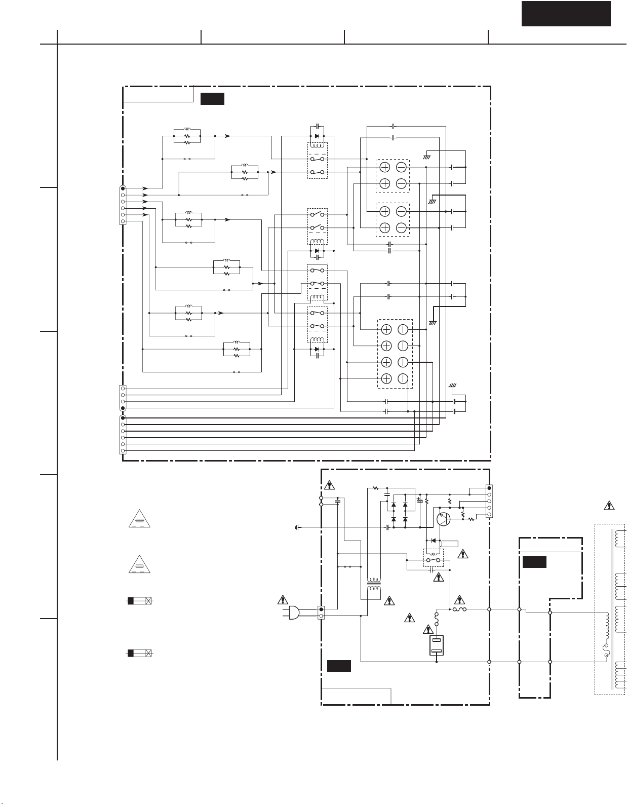
SCHEMATIC DIAGRAMS-4
SPEAKER TERMINAL & POWER SUPPLY SECTION
NAETC-8240
1
JL6803B
LSP
RSP
CSP
LSSP
RSSP
SBSP
TO NAAF-8245
2
JL6805B
BRLD
FRLD
TO NAAF-8245
3
CSRLD
+24V
LSPE
RSPE
CSPE
LSSPE
RSSPE
SBSPE
JL6804B
TO NAAF-8245
L6800 NC
R6800
R6810
J
L6802
R6802
R6812 NC
J
L6804
R6804
R6814
J
NC
NC
NC
NC
NC
NC
NC
U11
SPEAKER TERMINAL PC BOARD
C6800
D6800
RL6800
RL6801
D6801
C6801
RL6803
RL6804
D6804
C6804 103J
L6803
R6803
R6813 NC
J
L6805
R6805
R6815 NC
L6801
R6801
R6811 NC
J
NC
NC
NC
NC
J
NC
NC
103J
103Z
L
R
FRONT SPEAKERS-A
L
R
SURROUND
SPEAKERS
CENTER
SPEAKER
SURROUND
BACK
SPEAKER
C6842
C6845
C6840
NC
NC
C6841
FRONT
SPEAKERS-B
P6801
P6800
NC
C6846
C6847
NC
C6843
NC
NC
C6844
L
P6802
R
NC
NC
C6856
NC
C6857
NC
C6850
NC
C6851
NC
C6853
NC
C6854
NC
C6855
NC
C6852
NC
C921
C902
472M
/250VAC
CAUTION
FOR CONTINUED PROTECTION
AGAINST FIRE HAZARD, REPLACE
ONLY WITH FUSE OF SAME TYPE
VA
AND RATING INDICATED.
4
ATTENTION
AFIN D'ASSURER UNE PROTECTION
PERMANENTE CONTRE LES RISQUES
D'INCENDIE, REMPLACER UNIQUEMENT
VA
PAR UN FUSIBLE DE MEME TYPE
ET CALIBRATION COMME INDIQUE.
THIS SYMBOL LOCATED NEAR THE FUSE INDICATES
THAT THE FUSE USED IS SLOW OPERATING TYPE
FOR CONTINUED PROTECTION AGAINST FIRE
HAZARD,REPLACE WITH SAME TYPE FUSE. FOR FUSE
RATING REFER TO THE MARKING ADJACENT TO THE SYMBOL
CE SYMBOLE INDIQUE QUE LE FUSIBLE UTLISE EST
E LENT. POUR UNE PROTECTION PERMANENTE,N'UTILISER
QUE DES FUSIBLES DE MEME TYPE. CE DARNIER EST
INDIQUE LA QU LE PRESENT SYMBOL EST APPOSE.
NAAF-8245
P6907
P901
5
P917
P918
AC-H
AC-G
P901A
U19
POWER SUPPLY PC BOARD
NAPS-8248
8.2
R921
(1W)
223Z
D921
C923
223Z
D923
D921-D924
GP104003E OR
RL1N4003
T902
NPT-1492D
D922
D924
C922
100/35
C901
103M
/275VAC
F903
5A125V
R924 82
(1/2W)
D925
R926
(1W)
470
R922
R923
Q921
2SC2458-GR
2SC1740S-R,S
0.1V
RL901
F901
8A125V
P902
AC OUTLET
D:120W 1A MAX
+13VS
+13VS
MPUGND
POWER
1K
P912
P931A
P911
TO NNAF-8245
NAPS-8247
U18
TERMINAL
PC BOARD
P912A
3
7
P911A
T901
NPT-1494D
THERMAL FUSE
Page 20
NOTE
THE COMPONENTS IDENTIFIED BY MARK ARE CRITICAL FOR SAFETY
REPLACE ONLY WITH PART NUMBER SPECIFIED
VOLTAGE (MEASURED WITH VOLTMETER) IS DC VOLTAGE.(NO INPUT SIGNAL)
ALL PNP TRANSISTORS ARE EQUIVALENT TO 2SA1015-GR UNLESS OTHERWISE NOTED.
ALL NPN TRANSISTORS ARE EQUIVALENT TO 2SC1815-GR UNLESS OTHERWISE NOTED.
ALL DIODES ARE EQUIVALENT TO 1SS133 UNLESS OTHERWISE NOTED.
ELECTROLYTIC CAPACITORS ( ) ARE IN u F/WV.
ALL CAPACITORS ARE IN pF/50WV UNLESS OTHERWISE NOTED.
EX) 030- 3pF 330- 33pF 331- 330pF 333- 0.033uF
ALL RESISTORS ARE IN OHMS 1/4WATTS UNLESS OTHERWISE NOTED.
THE THICK LINES ON PC BOARD ARE THE PRINTING SIDE OF THE PARTS.
EX) PRINTING SIDE
CIRCUIT IS SUBJECT TO CHANGE FOR IMPROVEMENT.
IS DC VOLTAGE, AT NO INPUT SIGNAL.
<Notes>
NC=No mount of parts.
NAETC-8239
U10
TERMINAL PC BOARD
8
R9521
(1/2W)
3.3
9
C9513
223Z
JL9501B
JL9501A
NAETC-8238
U09
REGULATOR PC BOARD
5.6V
C6933
Q6931
TA78057S OR
NJM78M56FA
D6933
R6935
120
(2W)
PROTHERM
10/16
O
G
I
17.8V
C6932
103Z
C6931
1000/25
D6932
D6932,6933:
GP104003E OR
RL1N4003
PRO
SPF
+13VS
POWER
SPCS
S3GND
TO NAAF-8245
SPB
SE1H
VOLH
MPUGND
MPUGND
+24V
AGND
HPR
HPL
P6931A
P7503B
FLAC1
FLAC2
MPUGND
HPL
AGND
HPR
+5.6V
P410A
+24V
S3
S3GND
S3
S2
S2
S2
S2
+5.6V
PROTHERM
P411A
POWER
SPF
SPCS
SE1H
SPB
VOLH
PRO
MPUGND
+13VS
TO NADIS-8231
TO NADG-8230
TO NADG-8230
10
11
12
13
14
15
16
17
18
19
P995C
BLU
P995A
TO NAAF-8245
BLK
P995B
RED
0.47
R9501
1
F9501
R9503
0.22
R9502
(1/2W)
(1/2W)
NC
(1/2W)
NAPS-8249
U20
TERMINAL
PC BOARD
JL6952B
TO NAAF-8245
Page 21
HT-R820THX HT-R820THX
A
SCHEMATIC DIAGRAMS-5
POWER AMPLIFIER SECTION
NAAF-8245
1
2
SL
P6003
NF
-B1
+B1
B+
B-
TO NAAF-8235
SR
P6004
NF NF
-B1 -B1
+B1 +B1
B+ B+
B- B-
TO NAAF-8235
R6033
820
R6003
5.6K
R6013
3.9K
R6043
1K
R6053
3.9K
R6004
5.6K
R6014
3.9K
R6044
1K
R6054
3.9K
R6034
820
BCDEFGH
POWER AMPLIFIER PC BOARD
U16
1V
0.2V
Q6013
IID. ADJ.
-0.3V
1V
0.2V
Q6014
IID. ADJ.
-0.3V
-0.3V
-66.5V
-0.3V
-66.5V
1.1V
1.1V
(1/4W)
-1.1V
R6024
2.2
-1.1V
R6023
Q6023
Q6024
2.2
R6073
150
(1/4W)
(1/4W)
0.5V
-0.5V
Q6043
0.5V
R6074
150
(1/4W)
-0.5V
Q6044
C6043
47/50
Q6034
C6044
47/50
Q6033
P6083
ID+
ID-
P6084
ID+
ID-
R6083
2.2
(1/4W)
R6093
2.2
(1/4W)
C6233
473J
R6233
8.2
R6084
2.2
(1/4W)
R6094
2.2
(1/4W)
C6234
473J
R6234
8.2
(1W)
(1W)
0.5V
-0.5V
0.5V
-0.5V
0V
R6103
0.22X2
(2W)
0V
R6104
0.22X2
(2W)
Q6053
R6143
22K
C6053
0V
Q6063
Q6054
R6144
22K
C6054
0V
Q6064
66.5V
R6173
66.5V
Q6073
2SC2631-R,S
R6153
12K
47K
D6003
Q6074
2SC2631-R,S
R6154
12K
R6174
47K
D6004
R6163
33K
R6193
330K
R6183
R6164
33K
R6194
330K
D6013
47K
D6014
R6184
47K
P6011
E
E
E
E
E
E
E
E
E
TO NAAF-8235
1V
Q6015
-0.3V
-66.5V
1.1V
R6025
2.2
(1/4W)
Q6025
-1.1V
0.5V
R6075
150
(1/4W)
-0.5V
Q6045
Q6035
C6045
47/50
P6085
ID+
ID-
R6085
2.2
(1/4W)
R6095
2.2
(1/4W)
C6235
473J
R6235
8.2
(1W)
R6005
5.6K
R6015
3.9K
R6045
1K
R6055
3.9K
R6035
820
0.2V
IID. ADJ.
-0.3V
3
SB
P6005
NF NF
-B1 -B1
+B1 +B1
B+ B+
B- B-
TO NAAF-8235
4
D6903D6904
D10XB60H D10XB60H
C6901
12000/75
C6902
D6902
D6901
P6906
12000/75
C6903
104J
C6708
223J
D6706
D6705
NC
NC
TO NAPS-8248
5
TO NAPS-8248
P6907
P931
+13VS PRO
+13VS POWER
MPUGND RLGND
POWER POWER PROTHERM
TO NAAF-8249
C6905
334J
/100
C6904
334J/100
F6901
10A125V
C6907
104J
R6905
(1/2W)
0
R6904
(1/2W)
0
C6906
104J
P995CC
BLU
C6909
C6908
P995AA
BLK
RL6902
D6906
RL6901
NC
P995BB
NC
RED
66.5V
Q6055
0.5V
R6145
0V
22K
C6055
R6105
0.22X2
(2W)
0V
-0.5V
Q6065
TO NAPS-8249
Q6075
2SC2631-R,S
R6155
12K
R6175
47K
D6005
C6920
NC
0.1V
F6902
10A125V
JL6952A
R6165
33K
R6195
330K
Q6901
D6015
R6185
47K
0.8V
R6605
8.2
J011AJ011
J010AJ010
Refer to the following table about the parts displayed by mark " ".
REF NO. DESCRIPTION
Q6010-6015 2SC1740S-R,S
Q6020-6025 2SC1740S-R,S
Q6030-6032 KTD2061-Y OR 2SC5171
Q6033-6035 KTD2061-Y OR 2SC5171
Q6040-6042 KTB1369-Y OR 2SA1930
Q6043-6045 KTB1369-Y OR 2SA1930
Q6050-6051 2SC5242-O,R OR MN150S-Y,P,O
(1/2W)
Q6052-6055 2SC5242-O,R OR MN150S-Y,P,O
Q6060-6061 2SA1962-O,R OR MP150S-Y,P,O
R6902
Q6062-6065 2SA1962-O,R OR MP150S-Y,P,O
1K
Q6601-6603,Q6901 KTC3199-GR,2SC1740S-R,S,2SC2458-GR
Q6701,6702 KTC3200-BL,GR OR 2SC1775A-E,F OR 2SC1845-E,F
Q6303,6313
KTA1267-GR OR 2SA933S-R,S
Page 22

L
R6030
680
R6000
5.6K
P6000
R6010
3.9K
NF
-B1
+B1
B+
B-
R6040
TO NAAF-8235
1K
R6050
3.9K
R
R6031
680
R6001
5.6K
P6001
R6011
3.9K
R6041
TO NAAF-8235
1K
R6051
3.9K
C
R6032
680
R6002
5.6K
P6002
R6012
3.9K
R6042
TO NAAF-8235
1K
R6052
3.9K
1V
0.2V
Q6010
IID. ADJ.
-0.3V
1V
0.2V
Q6011
*
IID. ADJ.
-0.3V
1V
0.2V
Q6012
IID. ADJ
-0.3V
-0.3V
-66.5V
-0.3V
-66.5V
-0.3V
-66.5V
1.1V
1.1V
1.1V
R6020
2.2
Q6020
-1.1V
R6021
2.2
-1.1V
R6022
2.2
Q6022
-1.1V
(1/4W)
Q6040
(1/4W)
Q6021
Q6041
(1/4W)
0.5V
R6070
120
(1/4W)
-0.5V
0.5V
R6071
120
(1/4W)
-0.5V
0.5V
R6072
150
(1/4W)
-0.5V
Q6042
Q6030
C6040
47/50
Q6031
C6041
47/50
Q6032
C6042
47/50
P6080
ID+
ID-
P6081
ID+
ID-
P6082
ID+
ID-
R6080
2.2
(1/4W)
R6090
2.2
(1/4W)
C6230
473J
R6230
8.2
R6081
2.2
(1/4W)
R6091
2.2
(1/4W)
C6231
R6231
8.2
R6082
2.2
(1/4W)
R6092
2.2
(1/4W)
C6232
473J
R6232
8.2
473J
(1W)
(1W)
(1W)
0.5V
-0.5V
0.5V
-0.5V
0.5V
-0.5V
Q6050
0V
R6100
0.22X2
(2W)
0V
R6101
0.22X2
(2W)
0V
R6102
0.22X2
(2W)
66.5V
R6140
22K
C6050
0V
Q6060
R6170
D6000
66.5V
Q6051
R6141
22K
C6051
0V
Q6061
R6171
D6001
66.5V
Q6052
Q6072
2SC2631-R,S
R6142
22K
C6052
0V
Q6062
R6172
D6002
R6160
33K
Q6070
2SC2631-R,S
R6150
12K
R6190
330K
47K
R6161
33K
Q6071
2SC2631-R,S
R6151
12K
R6191
330K
47K
R6162
33K
R6152
12K
R6192
330K
47K
D6010
R6180
47K
D6011
R6181
47K
D6012
R6182
47K
NOTE
THE COMPONENTS IDENTIFIED BY MARK ARE CRITICAL FOR SAFETY
REPLACE ONLY WITH PART NUMBER SPECIFIED
VOLTAGE (MEASURED WITH VOLTMETER) IS DC VOLTAGE.(NO INPUT SIGNAL)
ALL PNP TRANSISTORS ARE EQUIVALENT TO 2SA1015-GR UNLESS OTHERWISE NOTED.
ALL NPN TRANSISTORS ARE EQUIVALENT TO 2SC1815-GR UNLESS OTHERWISE NOTED.
ALL DIODES ARE EQUIVALENT TO 1SS133 UNLESS OTHERWISE NOTED.
ELECTROLYTIC CAPACITORS ( ) ARE IN u F/WV.
ALL CAPACITORS ARE IN pF/50WV UNLESS OTHERWISE NOTED.
EX) 030- 3pF 330- 33pF 331- 330pF 333- 0.033uF
ALL RESISTORS ARE IN OHMS 1/4WATTS UNLESS OTHERWISE NOTED.
THE THICK LINES ON PC BOARD ARE THE PRINTING SIDE OF THE PARTS.
EX) PRINTING SIDE
CIRCUIT IS SUBJECT TO CHANGE FOR IMPROVEMENT.
IS DC VOLTAGE, AT NO INPUT SIGNAL.
NAETC-8255
TH1
COM
TH2
THERMAL SENSOR
U26
PC BOARD
Q6313
R6318
4.7K
R6317
470
R6306
10K
D6307
D6306
R6307
470
R6981
390
(1/2W)
JL6402A
TH1
+24V
TH2
24V
JL6402B
Q6303
0V
R6308
4.7K
LSPE
RSPE
CSPE
LSSPE
RSSPE
SBSPE
LSP
RSP
CSP
LSSP
RSSP
SBSP
R6980
390
(1/2W)
JL6804A
JL6803A
R6380
PTFL04BF
471Q2N34BO
R6381
PTFL04BC
471Q2N34B0
TO NAETC-8240
TO NAETC-8240
<Notes>
NC=No moune of pares.
C6701
220/6.3
R6701
22K
0V
D6701
R6702
C6703
10K
223Z
R6708
33K
Q6701 Q6702
D6702
+B1
C6704
1/50
Q6703
KTA1268-GR,BL
OR 2SA992-E,F
0V
C6716
100/6.3
R6704
47K
D6703
MTZJ5.1B
220K
R6706
D6714
MTZJ5.1B
D6704
MTZJ5.1B
C6706
100/6.3
5.6K
R6719
R6709
5.6K
R6710
12K
24V
Q6603
Q6601
0.05V
0.8V
R66011KR6603
1K
+13VS +13VS
24V
Q6602
0V
0V
R6602
1K
R6604
8.2
(1/2W)
BRLD
FRLD
CSRLD
+24V
HPL
HPR
E
+24V
MPUGND
VOLH
SEC1H
SPB
SPCS
SPF
JL6805A
TO NAETC-8240
P6931
TO NAETC-8238
Page 23
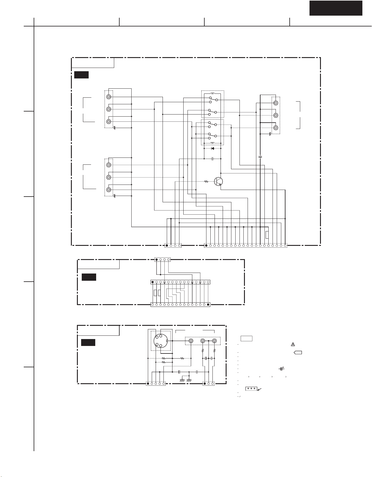
SCHEMATIC DIAGRAMS-6
VIDEO SECTION
HT-R820THX HT-R820THX
P253B
P261B
YC
P251
E301
P254
C263
104Z
C253
104Z
C261
471J
C262
471J
R251
75
R262
330
R261
330
R252
75
R253
75
NAETC-8234
VIDEO3 IN
SRLV
TO NAVD-8250 TO NADG-8230
U05
P243B
P242A
Q241
2SC1740
RL241
RL242
D241
R249
1K
C242
103Z
C241
103Z
P241
COMPONENT VIDEO
Y
CB(PB)
CR(PR)
P241
VIDEO 1/2/3 IN
Y
CB(PB)
CR(PR)
P241
DVD IN
Y
CB(PB)
CR(PR)
DGND
DGND
CNPT
+5V
CR2
CB2Y2CR1
CB1
Y1
CR
CB
GND
Y
CPNT
+5V
DGND
NAVD-8236
OUT
U07
COMPONENT VIDEO
NC
P206A
TO NAVD-8250
P801B
P243A
+12V
GND
GND
CNPT
RI
A
B
VMUT2
VMUT1
OPT2
DGND
OPT1
+5V
COAX
OPTOUT
NAETC-8243
TO NADG-8230
U14
COMPONENT VIDEO TERMINAL PC BOARD
TERMINAL
PC BOARD
VIDEO 3 TERMINAL
PC BOARD
NOTE
THE COMPONENTS IDENTIFIED BY MARK ARE CRITICAL FOR SAFETY
REPLACE ONLY WITH PART NUMBER SPECIFIED
VOLTAGE (MEASURED WITH VOLTMETER) IS DC VOLTAGE.(NO INPUT SIGNAL)
ALL PNP TRANSISTORS ARE EQUIVALENT TO 2SA1015-GR UNLESS OTHERWISE NOTED.
ALL NPN TRANSISTORS ARE EQUIVALENT TO 2SC1815-GR UNLESS OTHERWISE NOTED.
ALL DIODES ARE EQUIVALENT TO 1SS133 UNLESS OTHERWISE NOTED.
ELECTROLYTIC CAPACITORS ( ) ARE IN u F/WV.
ALL CAPACITORS ARE IN pF/50WV UNLESS OTHERWISE NOTED.
EX) 030- 3pF 330- 33pF 331- 330pF 333- 0.033uF
ALL RESISTORS ARE IN OHMS 1/4WATTS UNLESS OTHERWISE NOTED.
THE THICK LINES ON PC BOARD ARE THE PRINTING SIDE OF THE PARTS.
EX) PRINTING SIDE
CIRCUIT IS SUBJECT TO CHANGE FOR IMPROVEMENT.
IS DC VOLTAGE, AT NO INPUT SIGNAL.
<Notes>
NC=No moune of pares.
A
1
2
3
4
5
BCDEFGH
Page 24

P281
Y
C
P203
Y C
C
Y
P202
Y
C
C
Y
P201
NAETC-8243
P206B
Q281
74HCU04
1
2
3
4
5
6
7 8
9
10
11
12
13
14
P282
U283
U282
U281
P203
Q204
2SA933-S
KTA1267-GR
Q209
2SA933-S
KTA1267-GR
VIDEO OUT
VCC
VIN4
VIN3
VIN2
GND
VIN1
B
A
Q203
LA7956
1
2
3
4
5
6
7
8
9
VIDEO OUT
VCC
VIN4
VIN3
VIN2
GND
VIN1
B
A
Q213 LA7956
1
2
3
4
5
6
7
8
9
VIDEO OUT
VCC
VIN4
VIN3
VIN2
GND
VIN1
B
A
Q212 LA7956
1
2
3
4
5
6
7
8
9
P201
P202
Q201
RN1241
Q202
RN1241
Q208
RN1241
Q207
RN1241
Q210
RN1241
Q211
RN1241
NAETC-8234
P253A
Q205
DTA114ES
KRA102M
Q206
DTA114ES
KRA102M
L283
022M
L281
220K
NCH-1452
L282
220K
NCH-1452
D201
D202
C203
470/16
C201
2.2/50
C202
2.2/50
C204
2.2/50
C205
470/16
C221
47/16
C211
470/16
C209
2.2/50
C288
47/6.3
C285
47/6.3
C225
47/16
C223
47/16
C217
2.2/50
C218
2.2/50
C207
2.2/50
C213
2.2/50
C215
470/16
C289
223Z
C227
223Z
C220
223Z
C216
223Z
C222
223Z
C210
223Z
C208
223Z
C286
223Z
C281
223Z
C284
080D
C283
223Z
C226
223Z
C224
223Z
C219
223Z
C287
223Z
C282
101J
C206 223Z
C212
223Z
C214
223Z
R282
470
R223
100K
R230
680K
R205
75
R207
680K
R201
75
R210
220
R202
75
R208
680K
R209
680K
R203
75
R206
75
R204
100K
R228
220
R220 75
R219
75
R226
680K
R214
75
R213
75
R224
100K
R284
10K
R229
680K
R281
75
R225
680K
R212
75
R211
75
R217
100K
R218
100K
R216
75
R222
75
R221
75
R215 75
R227
680K
V4
V4Y
V4C
+12V
GND
A
B
VMUT2
VMUT1
RI
OPT2
DGND
OPT1
+5V
COAX
OPTOUT
NAVD-8250
VIDEO-2 IN
VIDEO-1
DVD IN
MONITOR
OUT
OUT
IN
OUT
IN
MONITOR
OUT
IN
VIDEO-2
VIDEO-1
DVD IN
U21
VIDEO PC BOARD
OPTICAL
1
OPTICAL
2
OPTICAL
3
COAXIAL
RI
REMOTE
CONTROL
Page 25

PC BOARD CONNECTION DIAGRAM
FM
U11 NAETC-8240
SPEAKER TERMINAL PC BOARD
TUNER UNIT
AC IN
JL6805C
JL6804C
JL6803C
U26
NAETC-8255
THERMAL SENSOR
PC BOARD
AM
VIDEO
RI
U21
NAVD-8250
VIDEO PC BOARD
P253A
DVD VIDEO TAPE
DIGITAL IN
P206B
HT-R820THX
U07
NAVD-8236
COMPONENT VIDEO TERMINAL
PC BOARD
COMPONENT VIDEO
P243B
U16
NAAF-8245
POWER AMPLIFIER
PC BOARD
F6901
F6902
P931
P6907
P995CC
BLU
SUB TRANS.
P917
P918
OUTLET
P901A
P911
U19
NAPS-8248
POWER SUPPLY
PC BOARD
U18
NAPS-8247
TERMINAL
PC BOARD
P911A P913A
MAIN TRANS.
JL9501B
U10
NAETC-8239
TERMINAL PC
BOARD
JL
6952A
P995BB
RED
T902
P913
F901
F903
JL6952B
P995B
RED
JL6805A
P995AA
BLK
P931A
P995C
P995A
BLU
BLK
U20
NAPS-8249
TERMINAL PC
BOARD
JL6402A
P6000
JL6803A
JL6804A
P6011
P6001
P6073A
P6002
P6003
P6004
P6072A
P6005
P6931
P6072
U12
NAETC-8241
HOLDER PC BOARD
U03
NASW-8232
OPERATION SWITCH
PC BOARD
JL7501B
JL7502B
P7501
U04
NAETC-8233
HEADPHONE TERMINAL
PC BOARD
402B
JL6
JL7502A
Q6050
Q6060
Q6051
Q6061
Q6052
Q6062
Q6053
Q6063
Q6054
Q6064
Q6055
Q6065
JL7501A
Q800
P6000A
P407A
P6011A
P6001A
P306A
P6002A
P6003A
P6004A
P6073
P6005A
P6931A
U01
NADG-8230
PRE-AMPLIFIER
PC BOARD
U06
NAAF-8235
DRIVER AMPLIFIER
PC BOARD
U09
JL9501A
FL TUBE
NAETC-8238
REGULATOR PC BOARD
P7503B
U02
NADIS-8231
DISPLAY PC BOARD
JUMPER WIRE SOCKET
FLAT CABLE
Q301
P406
P306
P101
Q701
Q7008
Q702
P7502B
P410B P411B
P411A
P410A
P7503A
U7501
BOARD TO BOARD
U14
NAETC-8243
TERMINAL
PC BOARD
P801
P206A
P801B
P261A
P7502A
S7501
P253B
U05
NAETC-8234
VIDEO 3 TERMINAL PC BOARD
P243A
P261B
Page 26
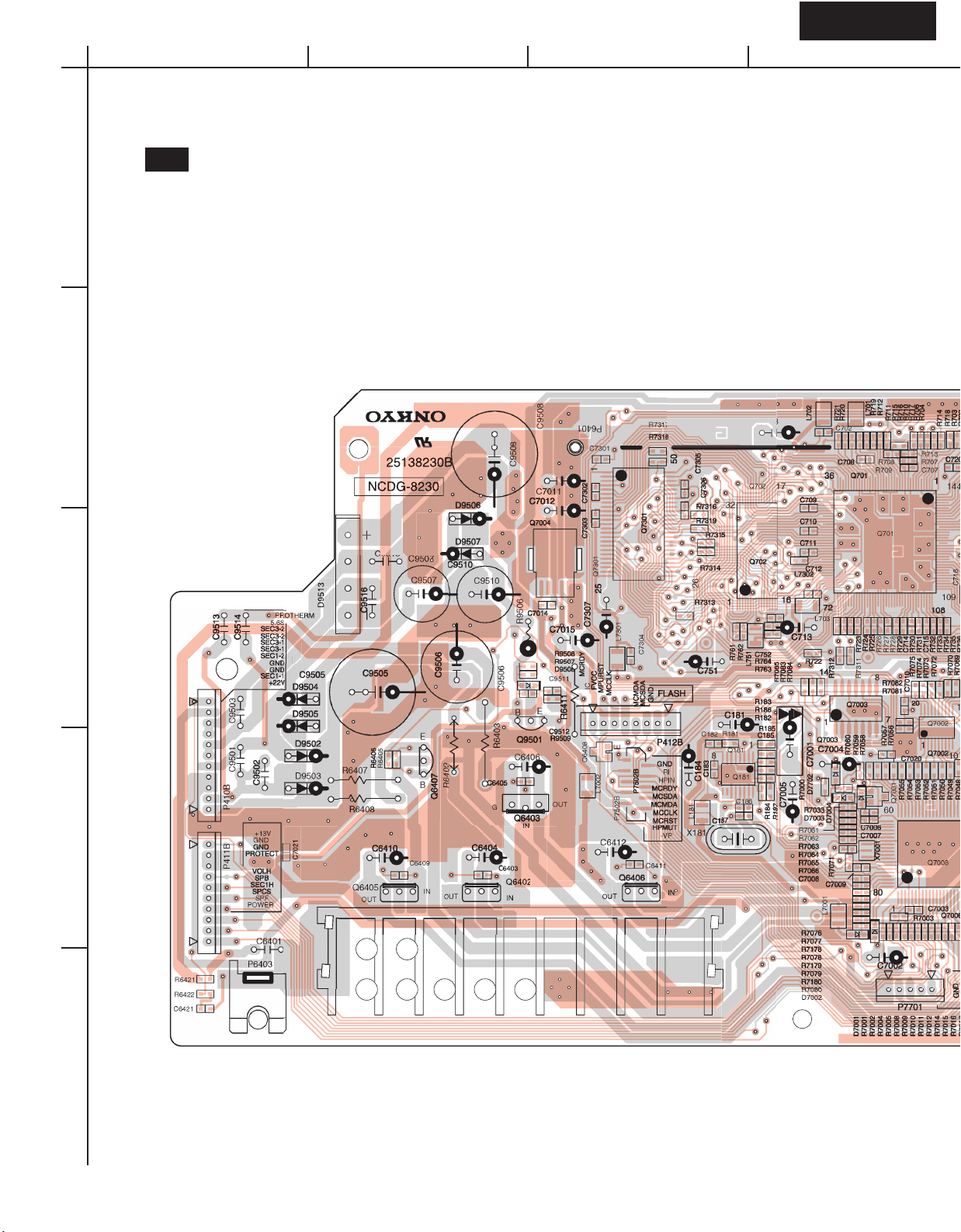
PRINTED CIRCUIT BOARD VIEWS-1
O
C70C7C703
019
020
120
U01
PREAMPLIFIER PC BOARD
(NADG-8230)
Component side
A
1
2
3
4
5
BCDEFGH
Page 27

HT-R820THXHT-R820THX
Page 28
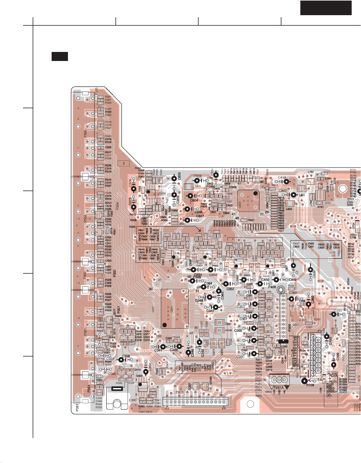
PRINTED CIRCUIT BOARD VIEWS-2
TUR
TUMUT
SD
STEREO
C82C82
C829
C831
C83
Q7008
Q
8
U01
PREAMPLIFIER PC BOARD (NADG-8230)
Soldering side
A
1
2
3
4
5
BCDEFGH
Page 29
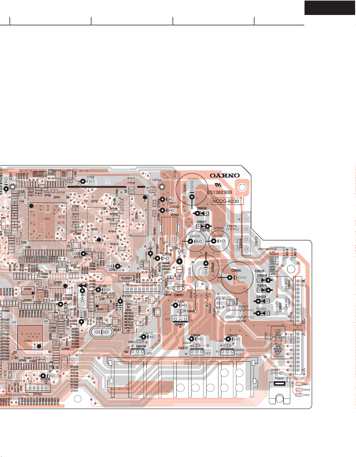
HT-R820THXHT-R820THX
Page 30
PRINTED CIRCUIT BOARD VIEWS-3
C75
513
C7
50
L7501A
Q75
Q
Q
507
50
513
R
S7611
S7612
S
S7622
S7623
S7625
S
S763
S
X7501
VIDE
VID
R
C
R
R7519
7634
7636
S7501
S
R9
R9
R
R9
RY
TUNER
CD
TUNIN
GND
N
G
N
N
N
D
C
CNCNC
C
C
N
5.6
HP-R
HP-G
HP-L
ND
GND
FAC2
U02
DISPLAY PC BOARD
(NADIS-8231)
Component side
A
1
2
3
4
5
BCDEFGH
Page 31

HT-R820THXHT-R820THX
C7
R7519
35
R763
S
S76
4
S7646
S7647
M
SETUP
NC
N
IC
C
ST
DI
D
D
DO
D
O
ND
N
D
5.6
HP-R
-G
HP-G
L
HP-L
GND
FAC2
75
513
C
C7
3
C
JL7501A
Q
7507
7507
75
1
31
R76
2
7633
S76
S
S7625
VIDEO
STBY
Page 32

HT-R820THX
V4L
V4L
4R
R
V4
GND
G
D
V4L
V4L
4R
R
V4
V
GND
G
D
7
JL
B
6
5
R7616
6
A
B
8
32
138232
7
JL7501B
6
R
6
A
B
2
5
38
3
JL7502B
33
25138233
7518
C7
L750
L7502
L7
C7519
C7519
C7520
50
501
JL7502B
JL7
7501
33
25138233
7518
C7
L7
L7
L7502
2
L7503
C7519
C7519
C7520
C5
3
2
1
34
1
C26
62
C262
C263
C253
51
25138234
51
C
C6
2
1
C
C263
C253
A
PRINTED CIRCUIT BOARD VIEWS-4
U03
1
2
U04
OPERATION SWITCH PC BOARD (NASW-8232)
Component side Soldering side
P
S761
17
7
P
7615
7501
1
7
HEADPHONE TERMINAL PC BOARD (NAETC-8233)
Component side Soldering side
BCD
761
S761
17
7
P
P
7615
2
W-
5
2
2
1
2
CSW-823
0
7615
R7593
7501
759
P7
3
U05
ETC-82
VIDEO 3 TERMINAL PC BOARD (NAETC-8234)
Component side
ETC-82
25
4
251
25
R2
Soldering side
1
251382
P251
5
262
2
261
2
26
Page 33

HT-R820THX
A
PRINTED CIRCUIT BOARD VIEWS-5
U06
1
2
3
4
5
DRIVER AMPLIFIER
PC BOARD (NAAF-8235)
Component side
BCD
E
E
Q5000
Q5010
R5050
R5020
R5010
C5010
R5000
C5000
E
B
R5041
C5011
R5001
C5001
E
B
C5012
R5002
C5002
E
B
C5013
R5003
C5003
E
B
C5014
R5004
C5004
E
B
C5015
R5005
C5005
J5003
J5014
J5006
J5016
J5018
Q5011
E
J5022
R5021
R5011
E
B
J5030
R5022
R5012
E
B
J5038
R5023
R5013
E
B
J5045
R5024
R5014
J5050
R5025
R5015
B
B
Q5012
Q5013
Q5014
Q5015
E
B
C5040
C5030
C5080
7
7
7
R5051
C5041
C5031
C5081
R5052
C5042
C5032
C5082
R5053
C5043
C5033
C5083
R5054
C5044
C5034
C5084
R5055
C5045
C5035
C5085
Q5050
Q5051
Q5052
Q5053
Q5054
Q5055
B
R5110
R5030
B
R5111
R5031
B
R5112
R5032
E
B
R5113
R5033
E
B
R5114
R5034
E
B
R5115
R5035
B
R5040
L
J5013
P5005
J5004
P407A
7
P406A
P306A
J5017
12
Q5001
22
J5015
P306A
E
L
E
R
E
RS
R
E
LS
E
7
C
E
J5024
SB
J5025
J5029
20
Q5002
R5042
CSL
30
J5033
J5032
20
J5037
J5034
Q5003
7
R5043
30
J5040 J5048
0
NCAF-8235
25138235
J5042
J5041
Q5004
7
R5044
30 25
SR
J5047
Q5005
R5045
SB
E
C5020
D5000
R5100
R5090
C5070
Q5030
BBE
J5005
J5007
J5008
J5010
J5011
J5012
E
C5021
D5001
R5101
R5091
C5071
Q5031
BBE
E
C5022
D5002
R5102
R5092
C5072
Q5032
BBE
C5023
D5003
R5103
R5093
C5073
Q5033
BBE
C5024
D5004
R5104
R5094
C5074
Q5034
BBE
C5025
D5005
R5105
R5095
C5075
Q5035
B
R5060
C5100
R5061
C5101
R5062
C5102
R5063
C5103
R5064
C5104
R5065
C5105
E
R5170
C5110
30
R5171
C5111
R5172
C5112
R5173
C5113
R5174
C5114
R5175
C5115
R5070
R5080
C5090
R5130
30
R5071
R5081
C5091
R5131
R5072
R5082
C5092
R5132
R5073
R5083
C5093
R5133
R5074
R5084
C5094
R5134
R5075
R5085
C5095
R5135
E
Q5040
J5002
R5140
R5160
R5190
30
30
30
27
27
E
Q5041
J5021
R5141
R5161
R5191
E
Q5042
J5028
R5142
R5162
R5192
E
Q5043
J5036
R5143
R5163
R5193
E
Q5044
J5044
R5144
R5164
R5194
P6073
EB
Q5045
J5049
R5145
R5165
R5195
P6000A
B-
B+
+B1
C5050
-B1
NF
J5001
R5180
20
P6011A
P5001
J5009
J5019
B-
C5051
B+
+B1
P6001A
-B1
NF
30
R5181
J5020
J5023
J5026
B-
B+
+B1
-B1
NF
C5052
P6002A
R5182
J5027
J5031
715
B-
B+
+B1
C5053
-B1
NF
P6003A
2225 15
R5183
J5035
J5039
P6004A
C5054
J5043
R5184
B-
B+
-B1
+B1
NF
J5046
B-
B+
C5055
-B1
+B1
NF
R5185
P6005A
Page 34

HT-R820THX
A
PRINTED CIRCUIT BOARD VIEWS-6
U07
COMPONENT VIDEO TERMINAL
PC BOARD (NAVD-8236)
1
2
U10
Component side
C
243
P241
P242A
15
OUTCOMPONENT1COMPONENT2
CB2
CR2
COMPONENT
J246
20
J247
22
P241
20
J242
Y1
Y2
CB1
CR1
22
J249
J248
7
TERMINAL PC BOARD
(NAETC-8239)
CR
J241
CB
RL242
Y
J243
RL241
BCD
U09
REGULATOR PC BOARD
(NAETC-8238)
Component side
J5216
J5218
S2S2S3
J5215
J5214
J5213
J5212
12
JL9501A
12
S3E
S3
S4
30
30
30
NCETC-8238
S4
25138238
0
J250
P243B
CPNT
C241
+5V
+5V
Q241
J244
DGND
C242
7
7
D241
CNPT
J245
DGND
DGND
J251
R249
25138236
NCVD-8236
0
P250
THERM
PRORLGND
+13VS
POWER
PRO
SPF
SPCS
SPB
SE1H
VOLH
MPUGND
MPUGND
+24V
AGND
HPR
HPL
P6931A
7
J5217
3
U12
Component side
4
U14
5
Component side
14 13 12 11 10 9 8
0
F9501
1.6A 125V
F9501B
R9503
HOLDER PC BOARD
(NAETC-8241)
0
P6072
25138241
NCETC-8241
TERMINAL PC BOARD
(NAETC-8243)
Component side
P243A
+5V
CNPT
DGND
DGND
NCETC-8239
25138239
F9501A
JL9501B
P206A
OPTOUT
COAX
+5V
OPT1
DGND
OPT2
RI
VMUT1
VMUT2
CTLB
CTLA
CNPT
GND
GND
+12V
R9501
R9502
J301
7
C9513
NCETC-8243
25138243
P801B
0
R9521
PROTHERM
+5.6V
S2
S2
S2
S2
S3
S3GND
S3GND
S3
P410A P411A
+24V
J5201
+13VS
MPUGND
MPUGND
PRO
VOLH
SPB
SE1H
SPCS
SPF
POWER
J5206
J5205
J5204
J5203
J5202
J5208
J5207
J5211
C6931
C6931
20
P7503B
P7503B
FLAC1
FLAC2
MPUGND
MPUGND
HPL
AGND
HPR
+5.6V
J5210
15
R6933
J5209
D6932
D6933
R6935
R6932
17
25
25
25
25
25
Q6931
OI
C6932
C6933
Page 35

A
BCDEFGH
PRINTED CIRCUIT BOARD VIEWS-7
1
HPL
HPR
AGND
+24V
MPUGND
MPUGND
VOLH
SE1H
SPB
R6980
SPCS
SPF
PRO
E
15
Q6075
B
J6191
POWER
+13VS
RLGND
P6931
2
THPRO
D6005
D6015
R6145
R6175
R6981
R6155
R6165
P6005
U16 POWER AMPLIFIER PC BOARD (NAAF-8245)
Component side
BCEBCE EBCEBCEBCEBCE
Q6065
12
17
C6055
R6185
J6190
J6189
15
R6195
Q6015
R6095
R6105 R6104
J6188
E
Q6025
E
J6187
Q6045
B
B
J6186
ID-ID+
R6055
NF
B+
B-
-B1
+B1
SB
27
Q6035
J6185
20
B
Q6055
J6184
J6179
J6183
17
J6180
17
J6181
17
J6182
C6045
Q6074
R6075
E
R6085
R6015
R6005
R6025
R6035
P6072A
20
1227
17 20
D6014
15
E
R6154
C6054
R6144
B
R6174
D6004
R6184
R6164
NF
-B1
Q6064
J6175J6178
J6172 J6161
17
17
J6174
J6169
R6194
P6084P6085 P6082
B+
+B1
R6094
J6171
E
Q6044
B
B-
J6170
ID-ID+
Q6024
R6054
P6004
E
B
J6168
Q6014
Q6034
Q6054
J6162
J6163
R6074
R6024
R6034
J6159
J6160J6176
22
R6084
R6014
R6004
J6158
C6044
J6165
J6152
Q6073
D6003
D6013
E
B
R6173
J6166
25
2512
12
12
25
B
E
221525
R6153
R6143
R6163
C6053
R6183
12
12
17
R6193
P6083
NF
-B1
20
J6150
J6151
17
17
J6146
+B1
Q6063
17
15
E
Q6043
B
B+
SLSR
J6167
R6719
C6716
D6714
J6157
7
J6156
J6155
J6154
J6142
NCAF-8245
R6093
J6153J6177
J6148
J6147
J6140
J6143
J6144
Q6023
E
Q6033
B
J6145
ID-ID+
R6053
R6043R6044R6045
B-
P6003
25138245A
EEEBBB
Q6013
R6103
Q6053
J6141
25
J6130
25
J6131
15
J6138J6149J6164J6173
20
J6135
15
J6136
J6139
15
J6137
12
J6133
12
J6134
B
C6043
R6073
R6023
1
R6083
R6013
R6003
R6033
C
Q6072
NF
D6002
-B1
E
3
U11 SPEAKER TERMINAL PC BOARD (NAETC-8240)
Component side
P6801
BL+
C6856
BR+
C6847
RL6801
4
BR-
C6846
BL-
P6801
L6800
RL6801
R6814
LSP
RSP
L6804
J5325
R6804
L6804
CSP
LSSP
C6801
RSSP
SBSP
J5324
R6813
L6803
27
15
J5323
J5322
L6803
7
J5327
R6803
JL6803B
7
J5319
C6857
R6810
L6800
J5320
R6800
J5321
L+
15
C6840
J5318
C6841
20
J5315
P6800
R6801
J5316
R+
L6801
27
J5312
P6800
L6801
J5317
L-
RL6800
R6811
NCETC-8240
25138240
30
C6850
20
R-
SL+
C6843
J5314
C6851
RL6800
25
J5313
12
J5309
15
J5308
0
J5310
7
J5311
SR+
J5326
RL6804
JL6804B
C6854C6853
RL6804
30
SL-
15
30
LSPE
J5307
RSPE
CSPE
C6844
17
LSSPE
RSSPE
SR-
J5306
SBSPE
P6802
P6802
D6800D6801
L6805
J5302
J5303
R6815
L6805
J5305
R6805
C6800
C+
SB+
C-
C6845
J5304
C6852
SB-
C6842
C6855
RL6803
RL6803
C6804
D6804
BRLD
FRLD
CSRLD
J5301
R6812
JL6805B
+24V
R6802
L6802
L6802
5
Page 36

HT-R820THXHT-R820THX
J6132
D6012
Q6072
R6152
R6142 J6116
BE
R6172
D6002
R6162
B+
B-
-B1
+B1
NF
25
R6318
SB-
D6804
BCEBCEBCEBCEBCEBCEBCE
Q6062
R6092
20
J6128
J6129
22 15
J6127 J6117
17
17
25
12
J6125
27
J6115 J6113
E
J6126
Q6042
R6192
C6052
B
ID-ID+
R6182
P6082
R6052
Q6012
J6122J6123
27
27
2017
R6102 R6101 R6100
12
J6119
J6120
J6114
Q6022
E
Q6032
B
R6042 R6041 R6040
J6098
J6118
25
J6112
B
C6042 C6041 C6040
E
R6072
R6082
R6012
R6002
R6022
R6032
P6002
Q6313
EB
J6109
7
J6111
J6110
J6108
7
J6192
J6124
P6073A
-B1
J011
J6107
7
J6100
J6047
R6904 R6905
C6904
J6101
P6909
D6706
C6708
D6705
J6094
J6095
17
17
R6306
R6706
R6704
C6905
Q6052
J6097J6121
Q6071
D6001
R6317
C6704
J6096
J6091
R6171
P6001
12
J6104
RL6901
EB
R6141
R6161
R6307
D6703
D6307
12
J6099
J6089
R6181 R6151
D6306
J6087
51A
JL69
D6011
12
J6073
C6051
P6081
NF
J6088
Q6303
22
R6191
-B1
RL6901
P995CC
P6907
25
J6090
+B1
BE
C6902
C6902
J6103
C6908
15
BLU
E
Q6041
B
B+
J6086
15
J6092
J6093
17
ID-ID+
B-
20
J6079
17
17
20
20
R6051
R
TH1
COM
TH2
P6301
R6308
7
J6085
RED
P995BB
Q6061
J6078
J6076
Q6021
E
B
J6074
J6070
27
30
J6084
7
R6091
J6080
J6075
J6077
J6072
25
P6922
J6105
J6083
7
POWER
Q6031
P6903
25
25
SBSPE
15
BLK
J6102
J6081
JL6952A
MPUGND
MPUGND
P931
22
B
E
30
LSSPE
RSSPE
J6066
12
J6106
J6063
+13VS
Q6011
R6021
12
P995
J6061
+13VS
27
27
15
J6056
J6049
J6050
R6071
R6081
R6011
R6001
R6031
J6071
J6067
JL6804A
J6069
A
A
15
J6062
J6064
J6065
RL6902
J6082
J6037
J6060
J6058
20
12
12
J6052
J6051
P6011
J6068
20
RL6902
25
20
J6057
CSPE
25
Q6051
J6059
J6053
J6054
J6055
JL6803A
SBSP
R6150
Q6070
R6140
BE
R6170
D6000
R6160
R6180
J6046
D6702
B
Q6701
LSPE
RSPE
C6901
C6901
7
J6042
30
30
J6043
D6904D6903
7
25
J6036 J6016
J6034
D6010
C6050
P6080
R6701
B
EE
J6045
RSSP
R6190
NF
7
J6044
27
CSP
LSSP
-B1
P6000
Q6702
J6038
RSP
E
J6048
Q6040
B
+B1
R6708
D6701
J6035
J6033
17
22
ID-ID+
B+
20
J6041
J6031
J6032
17
LSP
17
J6025
R6050
B-
Q6703
R6709
C6701
22
12
20
15
Q6020
J6024
B
E
J6040
20
C6906
J6015
Q6060
17
J6022
E
B
R6710
R6090
J6029
J6023
R6702
C6706
30
C6907
20
J6026
Q6030
L
C6703
D6704
+B1
J010
P6923
J6027
J6017
D6901
EEEEB B B
Q6010
J6014
-B1
J011A
1522
J6013J6030
20
J6009J6028
15
J6010
15
J6011
17
J6012
17
J6005
27
J6006
17
R6070
R6010
R6000
R6020
R6030
JL6402A
R6080
TH1
TH2
J6007
+24V
B
E
R6234
R6232
R6233
30
R6235
30
R6605
J6019
E
E
E
J6002
J6003
Q6603
Q6602
Q6601
R6604
R6602
R6902
J6020
C6920
D6906
J6001J6018
C6909
F6901B
F6902B
F6902
F6901A
F6902A
C6903
D6902
Q6050Q6053
+B1
B
R6603
B
B
R6601
E
B
P6910
J6004
R6231
R6230
Q6901
JL6805A
F6901
J010A
P
6
9
25
JL6803D
P6983
C6235
C6234
30
C6233
C6232
C6231
C6230
P6981
+24V
CSRLD
FRLD
BRLD
10A 125V
8
2
LSP
RSP
CSP
LSSP
RSSP
SBSP
J6008
P6906
Page 37

HT-R820THX
A
PRINTED CIRCUIT BOARD VIEWS-8
U18
1
U19
2
3
TERMINAL PC BOARD
(NAPS-8247)
Component side
731
J6201
P911A
NCPS-8247
25138247
0
5
J6202
P912A
J6203
P913A
POWER SUPPLY PC BOARD (NAPS-8248)
Component side
S902
S902
P923A
25
T902
1234
T902
R921
J6320
D923
D924
D921
D922
C922
P931A
C921
E
R926
C923
P922A
120V220V
J6309
P921A
(JDPG)
D925
Q921
R922
(W)
R923
12
J6308
56789
578
R924
B
+13VS
+13VS
MPUGND
MPUGND
POWER
P917
T3.15AL250V
P913
P923
RL901
BCD
U20
TERMINAL PC BOARD
(NAPS-8249)
Component side
19 18 17 16 15
NCPS-8249
25138249
0
J6408
J6406
J6409
J6404
J6403
12
J6411
P995A
BLK
P995B
RED
12
JL6952B
J6407
22
12
J6405
J6402
J6401
17
17
J6410
Component side
R6381R6380
TH1
+24V
TH2
JL
6
40
2
B
NCETC-8255
P6380
25138255
0
F902A
F902
RL901
(JD)
7
F902B
7
(PG)
J6317
C902
(P)
J6306
J6313
C902
P925
()
7
30
F901A
P921
C901
J6412
J6413
P995C
L6951B
J
BLU
NNLL
P902
P912
P922
12
(JDPG)
7
J6316
P902
8A 125V
()
J6315
J6318
7
()
J6319
P926
27
F903AF903B
(J)
22
J6304
J6312
15
J6301
17
P918
J6314
F901
F901B
C901
J6302
12
AC-GAC-H
P909 P908
J6310
5A 125V
30
F903
P911
AC-H
AC-G
R901
P901A
25138248
NCPS-8248
0
U26
THERMAL SENSOR
PC BOARD
(NAETC-8255)
TH1 TH2
4
U21
VIDEO PC BOARD
(NAVD-8250)
Component side
5
P206B
U283
C280
J249
J243
OPTOUT
COAX
+5V
OPT1
DGND
OPT2
VM1
VM2
CNPT
J252
J216
7
GND
GND
C288
J217
J236
12
J254
R224
R223
U281
U281
J247
C287
17
C282
R281
C283
L283
NCVD-8250
25138250
J239
17
12
Q201
J242
7
12
J228
J229
17
17
C218
C224
P281
P281
C281
J248
R282
C206
R212
1
J224
7
B
B
B
Q208
Q207
E
E
E
J223
7
J227
J232
J231
J205
Q212
C221
J209
J233
J207
C201
R209
R201
J210
R230
R211
17
R219
J220
J204
P282
C207
P282
D201
20
C223
J212
R207
C222
D202
C210
J241
R210
P201
P201
C227
R205
C208
C211
15
Q203
J203
J211
12
J213
Q204
C203
J226
7
B
R227
E
J206
J240
J221
7
R208
15
R229
1515
R220
C209
J225
R214
12
J215
C226
C225
C202
C212
R225
Q202
R226
B
E
R202
C204
Q210
J219
J222
J202
R216
B
E
R213
C213
R228
R221
C214
Q211
C220
B
Q209
Q213
P203
R203
R206
C205
E
BE
P203
P299
C215
P202
R215
R218
P202
R204
R222
P204
C216
R217
P204
U282
12
7
U282
J244
U283
C289
J251
J246
J255
1
J230
Q281
Q281
C219
L282
L281
C240
J253
7
C284
R284
C286
Q206
C285
BB
E
J238
E
Q205
C217
P253A
P253A
J250
1
Q281
15
7
J237
15
RI
B
A
+12V
Page 38

IC BLOCK DIAGRAM AND TERMINAL DESCRIPTIONS-1
Q181: BU1924FS (RDS decoder)-1
BLOCK DIAGRAM
TX-SR502/E/8250/HT-R520
MUX
Vref
DD1
V
SS1
V
VDD2
SS2
V
100k
(4)
120k
100k
PLL
57kHz
RDS/ARI
XO
anti-aliasing
filter
PLL
1187.5Hz
Reference
clock
(3)
(5)
Analog
Power supply
(6)
(12)
Digital
Power supply
(11)
(13) (14) (10) (9)
XI
8th Switched
capacitor filter
Bi-phase
decoder
VSS3
(7) (8)
Measurement
circuit
T1 T2
CMP
comparator
Differential
decoder
(16)
(1)
(2)
RCLK
QUAL
RDATA
TERMINAL DESCRIPTION
10
11
12
13
14
15
16
1
2
3
4
5
6
7
8
9
Pin name
QUAL
RDATA
Vref
MUX
DD1
V
V
SS1
VSS3
CMP
T2
T1
VSS2
VDD2
XI
XO
(N.C.)
RCLK
Description
Output terminal of demodulator quality signal.
Output terminal of demodulator data.
Input terminal of reference voltage.
Input terminal of composite signal.
Analog power supply.
Analog power supply.
Ground.
Input terminal of comparator.
Input terminal for test mode.
Input terminal for test mode.
Digital power supply.
Digital power supply.
Connect to oscillator.
Connect to oscillator.
---
Output terminal of demodulator clock.
Pin No.
Page 39

IC BLOCK DIAGRAM AND TERMINAL DESCRIPTIONS-2
Q212,213: LA7956 (Video switch)
BLOCK DIAGRAM
6dB
amp
TX-SR502/E/8250/HT-R520
TRUTH TABLE
driver control
123 4
VIDEO
S2
(Pin 2)
H
L
H
L
A B VINI5GND6VIN27VCC8VIN39VIN4
OUT
S3
(Pin 3)
H
H
L
L
Vin1
(Pin 4)
ON
OFF
OFF
OFF
Vin2
(Pin 6)
OFF
ON
OFF
OFF
video switch
(4input 1output)
Vin3
(Pin 8)
OFF
OFF
ON
OFF
Vin4
(Pin 9)
OFF
OFF
OFF
ON
Page 40

IC BLOCK DIAGRAM AND TERMINAL DESCRIPTIONS-3
Q291: BU4053B (Triple 2- channel analog multiplexer/ demultiplexer)
BLOCK DIAGRAM
VDD (16)
INH (6)
A (11)
B (10)
C (9)
VSS (8)
VEE (7)
X0 (12)
X1 (13)
Y0 (2)
Y1 (1)
Z0 (5)
Z1 (3)
TRUTH TABLE
LEVEL
CONVERTER
BINARY TO 1of 2
DECODER WITH INH
(14) X
(15) Y
(4) Z
TX-SR502/E/8250/HT-R520
ON SWITCH
INH
L
L
L
L
LLLH X0 Y0 Z1
LHLH X1 Y0 Z1
LLHH X0 Y1 Z1
LHHH X1 Y1 Z1
H X X X NONE
X:lrrelevant
A
L
H
L
H
B
L
L
H
H
C
L
L
L
L
X
0 Y0 Z0
X1 Y0 Z0
X0 Y1 Z0
X1 Y1 Z0
Page 41

IC BLOCK DIAGRAM AND TERMINAL DESCRIPTIONS-4
Q301: BD3817KS (7ch Volume with 10ch input selector)-1
BLOCK DIAGRAM
AGND15
OUT299OUT198AGND1497ROUTC296ROUTC195ROUTB294ROUTB193ROUTA292ROUTA191AGND1390VCC89NC88VEE87AGND1286DA85CL84MUTE83THGND82GOUTFR
100
VEE
CC
AGND1 1
AGND2
INA1
INA2 4
INB1 5
INB2 6
INC1
INC2 8
IND1
IND2 10
INE1 11
INE2 12
INF1
INF2 14
ING1 15
ING2 16
INH1
INH2 18
INI1
INI2 20
INJ1
INJ2
AGND3 23
INDVDFR
INDVDFL
INDVDC
INDVDSR
INDVDSL
INDVDCB
INDVDSW 30
2
Input
select2
3
7
9
13
17
19
21
22
24
25
26
27
28
29
Input
select1
V
6.1ch select
FRL select
Maser
volume
LOGIC
Output
mode
select
TX-SR502/E/8250/HT-R520
81
VINFR80
GOUTFL
79
78
VINFL
AGND1177
TREBLE
BASS
TNF176
TNF275
74
BNFA1
BNFB173
72
BNFA2
BNFB271
OUTFR70
NC69
68
OUTFL
AGND1067
OUTC66
OUTSR65
64
OUTSL
OUTCB63
62
AGND9
OUTSW61
NC
60
59
AGND8
VINC58
57
GOUTC
56
VINSR
GOUTSR
55
54
VINSL
53
GOUTSL
52
VINCB
GOUTCB51
31 32
AGND4
34NC35
AUTO133AUTO2
36NC37NC38
AGND5
39
INDSPFL
INDSPFR
40
INDSPC
41
INDSPSR
42
INDSPSL
43
INDSPCB
44
45NC46
INDSPSW
47NC48
AGND6
49
VINSW
GOUTSW
50
AGND7
Page 42

IC BLOCK DIAGRAM AND TERMINAL DESCRIPTIONS-5
Q301: BD3817KS (7ch Volume with 10ch input selector)-2
TERMINAL DESCRIPTION
TX-SR502/E/8250/HT-R520
Pin No. Pin Name Description
Analog ground terminal
Analog ground terminal
1ch input terminal A
2ch input terminal A
1ch input terminal B
2ch input terminal B
1ch input terminal C
2ch input terminal C
1ch input terminal D
2ch input terminal D
1ch input terminal E
2ch input terminal E
1ch input terminal F
2ch input terminal F
1ch input terminal G
2ch input terminal G
1ch input terminal H
2ch input terminal H
1ch input terminal I
2ch input terminal I
1ch input terminal J
2ch input terminal J
Analog ground terminal
FRch DVD input terminal
FLch DVD input terminal
Cch DVD input terminal
SRch DVD input terminal
SLch DVD input terminal
CBch DVD input terminal
SWch DVD input terminal
Analog ground terminal
1ch A/D output terminal
2ch A/D output terminal
Non-connected terminal
Analog ground terminal
Non-connected terminal
Non-connected terminal
FRch DSP input terminal
FLch DSP input terminal
Cch DSP input terminal
SRch DSP input terminal
SLch DSP input terminal
CBch DSP input terminal
10
11
12
13
14
15
16
17
18
19
20
21
22
23
24
25
26
27
28
29
30
31
32
33
34
35
36
37
38
39
40
41
42
43
1
2
3
4
5
6
7
8
9
AGND1
AGND2
INA1
INA2
INB1
INB2
INC1
INC2
IND1
IND2
INE1
INE2
INF1
INF2
ING1
ING2
INH1
INH2
INI1
INI2
INJ1
INJ2
AGND3
INDVDFR
INDVDFL
INDVDC
INDVDSR
INDVDSL
INDVDCB
INDVDSW
AGND4
AOUT1
AOUT2
NC
AGND5
NC
NC
INDSPFR
INDSPFL
INDSPC
INDSPSR
INDSPSL
INDSPCB
Pin No. Pin name Description
44
45
46
47
48
49
50
51
52
53
54
55
56
57
58
59
60
61
62
63
64
65
66
67
68
69
70
71
72
73
74
75
76
77
78
79
80
81
82
83
84
85
86
INDSPSW
NC
AGND6
NC
GOUTSW
VINSW
AGND7
GOUTCB
VINCB
GOUTSL
VINSL
GOUTSR
VINSR
GOUTC
VINC
AGND8
NC
OUTSW
AGND9
OUTCB
OUTSL
OUTSR
OUTC
AGND10
OUTFL
NC
OUTFR
BNFB2
BNFA2
BNFB1
BNFA1
TNF2
TNF1
AGND11
VINFL
GOUTFL
VINFR
GOUTFR
THGND
MUTE
CL
DA
AGND12
SWch DSP input terminal
Non-connected terminal
Analog ground terminal
Non-connected terminal
SWch input gain output terminal
SWch volume input terminal
Analog ground terminal
CBch input gain output terminal
CBch volume input terminal
SLch input gain output terminal
SLch volume input terminal
SRch input gain output terminal
SRch volume input terminal
Cch input gain output terminal
Cch volume input terminal
Analog ground terminal
Non-connected terminal
SWch output terminal
Analog ground terminal
CBch output terminal
SLch output terminal
SRch output terminal
Cch output terminal
Analog ground terminal
FLch output terminal
Non-connected terminal
FRch output terminal
2ch bass filter terminal B
2ch bass filter terminal A
1ch bass filter terminal B
1ch bass filter terminal A
2ch treble filter terminal
1ch treble filter terminal
Analog ground terminal
FLch volume input terminal
FLch input gain output terminal
FRch volume input terminal
FRch input gain output terminal
Comparator ground terminal
Mute terminal
Serial clock input terminal
Serial data and latch input terminal
Analog ground terminal
Page 43

IC BLOCK DIAGRAM AND TERMINAL DESCRIPTIONS-6
Q301: BD3817KS (7ch Volume with 10ch input selector)-3
TERMINAL DESCRIPTION
Pin No. Pin Name Description
87
88
89
90
91
92
93
94
95
96
97
98
99
100
VEE
NC
VCC
AGND13
ROUTA1
ROUTA2
ROUTB1
ROUTB2
ROUTC1
ROUTC2
OUT1
OUT2
AGND14
AGND15
(-)Power supply terminal
Non-connected terminal
(+)Power supply terminal
Analog ground terminal
1ch REC input and output terminal A
2ch REC input and output terminal A
1ch REC output terminal B
2ch REC output terminal B
1ch REC output terminal C
2ch REC output terminal C
1ch output terminal
2ch output terminal
Analog ground terminal
Analog ground terminal
TX-SR502/E/8250/HT-R520
Page 44

IC BLOCK DIAGRAM AND TERMINAL DESCRIPTIONS-7
Q701: CS494003CQZ (Multi-Standard Audio Decoder)-1
BLOCK DIAGRAM
TX-SR502/E/8250/HT-R520
Compressed
Digital
Interface
Digital
Audio
Input
DSP AB
PLL Clock
Manager
PIN LAYOUT
CMPCLK, FSCLKN2
CMPREQ, FLRCLKN2
CMPDAT, FSDATAN2
FSCLKN1, STCCLK2
UHS2, CS_OUT, GPIO17
Frame
Shifter
Input
Buffer
RAM
AUDATA1
AUDATA0
HDATA2, GPIO2
HDATA1, GPIO1
HDATA0, GPIO0
WR, DS, GPIO10
RD, R/W, GPIO11
SCDOUT, SCDIO
VSS3
VDD3
FLRCLKN1
PLLVSS
FILT2
FILT1
PLLVDD
XTALO
CLKIN, XTALI
CLKSEL
CS, GPIO9
A0, GPIO13
FSDATAN1
VDD4
VSS4
SCS
SCDIN
VSS5
VDD5
A1, GPIO12
HINBSY, GPIO8
SCCLK
RESET
LRCLK0
110
115
120
125
130
135
140
144
1
UHS0, GPIO18
Multi-Standard
Audio Decoder
Parallel or Serial
Host Interface
4, GPIO4
AUDATA3, XMT958A
AUDATA2
INTREQ
UHS1, GPIO19
AUDATA4, GPIO28
HDATA
HDATA3, GPIO3
SCLK0
105
5
GPIO20
FA1, FSCDIN
FAO, FSCCLK
FHS2, FSCDIO, FSCDOUT
VSS2
VDD2
100
FDAT7
GPIO21
HDATA5, GPIO5
MCLK
SCLK1
10
VSS6
VDD6
FHS0, FWR, FDS
Shared Memory
AUDATA5, GPIO29
AUDATA6, GPIO30
HDATA7, GPIO7
AUDATA7, XMT958B, GPIO31
HDATA6, GPIO6
95
15
FCS
FDAT6
FDBCK
FINTREQ
FHS1, FRD, FR/W
VSS1
VDD1
90
FDAT4
FDAT5
SAI 0
SAI 1
SAI 2
SAI 3
DSP C
DSP
RAM
NC2
NC1
20
VSS7
VDD7
Serial
Audio
Interface
Programmable
32-Bit DSP
NC4
NC3
LRCLKN, GPIO23
SCLKN, GPIO22
LRCLK1
85
25
DBCK
DBDA
FDAT2
FDAT3
FDBDA
DSP
ROM
SDATAN1, GPIO25
SDATAN3, GPIO27
SDATAN0, GPIO24
SDATAN2, GPIO26
SD_RAS
SD_CAS
80
30
TEST
FDAT0
FDAT1
NV_CS, GPIO14
NV_OE, GPIO15
NV_WE, GPIO16
External Memory
Interface
Digital
Audio
Output
Internal Bus
GPIO and I/O
Controller
Parallel or Serial
Host Interface
R1 ,EXTA1
SD_ADD
SD_ADDR2 ,EXTA2
SD_ADDR0, EXTA0
SD_ADDR3 ,EXTA3
75
SD_ADDR10, EXTA10
SD_BA, EXTA19
70
VDDSD1
VSSSD1
SD_CS
SD_ADDR4, EXTA4
SD_ADDR5, EXTA5
65
SD_ADDR6, EXTA6
SD_CLK_EN
SD_ADDR7, EXTA7
SD_ADDR8, EXTA8
SD_CLK_IN
60
SD_ADDR9, EXTA9
SD_CLK_OUT
VDDSD2
VSSSD2
SD_DATA8, EXTA11
55
SD_DATA9, EXTA12
SD_DATA10, EXTA13
SD_DATA11, EXTA14
SD_DATA12, EXTA15
VDDSD3
50
VSSSD3
SD_DATA13, EXTA16
NC5
SD_DATA14, EXTA17
SD_DATA15, EXTA18
45
SD_DQM1
SD_DATA7, EXTD7
SD_DATA6, EXTD6
VDDSD4
VSSSD4
40
SD_DATA5, EXTD5
SD_DQM0
SD_DATA4, EXTD4
SD_DATA3, EXTD3
35
SD_WE
SD_DATA2, EXTD2
SD_DATA1, EXTD1
SD_DATA0, EXTD0
DAO 0
DAO 1
Page 45

TX-SR502/E/8250/HT-R520
IC BLOCK DIAGRAM AND TERMINAL DESCRIPTIONS-8
Q701: CS494003CQZ (Multi-Standard Audio Decoder)-2
TERMINAL DESCRIPTION
FILT1 - Phase-Locked Loop Filter
Connects to an external filter for the on-chip phase-locked loop.
FILT2 - Phase Locked Loop Filter
Connects to an external filter for the on-chip phase-locked loop.
CLKIN, XTALI - External Clock Input/Crystal Oscillator Input
CS494003 clock input. This pin accepts an external clock input signal that is used to drive the internal core logic. When in internal clock
mode (CLKSEL == VSS), this input is connected to the internal PLL from which all internal clocks are derived. When in external clock
mode (CLKSEL == VDD), this input is connected to the DSP clock. Alternatively, a 12.288 mhZ crystal oscillator can be connected between
XTALI and XTALO. INPUT
XTALO - Crystal Oscillator Output
Crystal oscillator output. OUTPUT
CLKSEL - DSP Clock Select
This pin selects the internal source clock. When CLKSEL is low, CLKIN is connected to the internal PLL from which all internal clocks are derived.
When CLKSEL is high, the PLL is bypassed and the external clock directly drives all input logic. INPUT
FDAT0~FDAT7 - DSPAB Bidirectional Data Bus
In parallel host mode, these pins provide a bidirectional data bus to DSPAB. These pins have an internal pull-up.
BIDIRECTIONAL - Default: INPUT
FA0, FSCCLK - Host Parallel Address Bit Zero or Serial Control Port Clock
In parallel host mode, this pin serves as one of two address input pins used to select one of four parallel registers. In serial host mode, this pin serves
as the serial control clock signal, specifically as the SPI clock input. INPUT
FA1, FSCDIN - Host Address Bit One or SPI Serial Control Data Input
In parallel host mode, this pin serves as one of two address input pins used to select one of four parallel registers. In SPI serial host mode, this pin serves
as the data input. INPUT
FHS1, FRD, FR/W - Mode Select Bit 1 or Host Parallel Output Enable or Host Parallel R/W
DSPAB control port mode select bit 1. This bit is one of 3 control port select bits that are sampled on the rising edge of RESET to determine the control
port mode of DSPAB. In Intel parallel host mode, this pin serves as the active-low data bus enable input. In Motorola parallel host mode, this pin serves
as the read-high/write-low control input signal. In serial host mode, this pin can serve as the external memory active-low data-enable output signal.
BIDIRECTIONAL - Default: INPUT
FHS0, FWR, FDS - Mode Select Bit 0 or Host Write Strobe or Host Data Strobe
DSPAB control port mode select bit 0. This bit is one of 3 control port select bits that are sampled on the rising edge of RESET to determine the control
port mode of DSPAB. In Intel parallel host mode, this pin serves as the active-low data-write-input strobe. In Motorola parallel host mode, this pin
serves as the active-low data-strobe-input signal. In serial host mode, this pin can serve as the external-memory active-low write-enable output signal.
BIDIRECTIONAL - Default: INPUT
FCS - Host Parallel Chip Select, Host Serial SPI Chip Select
In parallel host mode, this pin serves as the active-low chip-select input signal. In serial host SPI mode, this pin is used as the active-low chip-select input
signal. INPUT
FHS2, FSCDIO, FSCDOUT - Mode Select Bit 2 or Serial Control Port Data Input and Output, Parallel Port Type Select
DSPAB control port mode select bit 2. This bit is one of 3 control port select bits that are sampled on the rising edge of RESET to determine the control
port mode of DSPAB. In SPI mode this pin serves as the data output pin. In parallel host mode, this pin is sampled at the rising edge of RESET to
configure the parallel host mode as an Intel type bus or as a Motorola type bus. BIDIRECTIONAL - Default: INPUT
FINTREQ - Control Port Interrupt Request
Open-drain interrupt-request output. This pin is driven low to indicate that the DSP has outgoing control data that should be read by the host.
OPEN DRAIN I/O - Requires 3.3K Ohm Pull-Up
FSCLKN1, STCCLK2 - PCM Audio Input Bit Clock
Digital-audio bit clock input. FSCLKN1 operates asynchronously from all other DSPAB clocks. In master mode, FSCLKN1 is derived from DSPAB's
internal clock generator. The active edge of FSCLKN1 can be programmed by the DSP.
BIDIRECTIONAL - Default: INPUT
Page 46

TX-SR502/E/8250/HT-R520
IC BLOCK DIAGRAM AND TERMINAL DESCRIPTIONS-9
Q701: CS494003CQZ (Multi-Standard Audio Decoder)-3
TERMINAL DESCRIPTION
FLRCLKN1 - PCM Audio Input Sample Rate Clock
Digital-audio frame clock input. FLRCLKN1 typically is run at the sampling frequency. FLRCLKN1 operates asynchronously from all other DSPAB
clocks. The polarity of FLRCLKN1 for a particular subframe can be programmed by the DSP.
BIDIRECTIONAL - Default: INPUT
FSDATAN1 - PCM Audio Data Input One
Digital-audio data input that can accept from one compressed line or 2 channels of PCM data. FSDATAN1 can be sampled with either edge of
FSCLKN1, depending on how FSCLKN1 has been configured. INPUT
CMPCLK, FSCLKN2 - PCM Audio Input Bit Clock
Digital-audio bit clock input. FSCLKN2 operates asynchronously from all other DSPAB clocks. The active edge of FSCLKN2 can be programmed
by the DSP.
BIDIRECTIONAL - Default: INPUT
CMPDAT, FSDATAN2 - PCM Audio Data Input Number Two
Digital-audio data input that can accept either one compressed line or 2 channels of PCM data. FSDATAN2 can be sampled with either edge of
FSCLKN2, depending on how FSCLKN2 has been configured.
BIDIRECTIONAL - Default: INPUT
FDBCK - Reserved
This pin is reserved and should be pulled up with an external 3.3k resistor. INPUT
FDBDA - Reserved
This pin is reserved and should be pulled up with an external 3.3k resistor.
BIDIRECTIONAL - Default: INPUT
PLLVDD - PLL Supply Voltage
2.5 V PLL supply.
PLLVSS - PLL Ground Voltage
PLL ground.
RESET - Master Reset Input
Asynchronous active-low master reset input. Reset should be low at power-up to initialize the DSP and to guarantee that the device is not active during
initial power-on stabilization periods. At the rising edge of reset the host interface mode of DSPAB is selected contingent on the state of the FHS0,
FHS1, and FHS2 pins. At the rising edge of reset the host interface mode of DSPC is selected contingent on the state of the UHSO, UHS1, and
UHS2 pins. If reset is low all bidirectional pins are high-Z inputs. INPUT
TEST - Reserved
This should be tied low for normal operation. INPUT
MCLK - Audio Master Clock
Bidirectional master audio clock. As an output, MCLK provides a low jitter oversampling clock.
MCLK supports all standard oversampling frequencies. BIDIRECTIONAL - Default: INPUT
SCLK0 - Audio Output Bit Clock
Bidirectional digital-audio output bit clock for AUDATA0, AUDATA1, AUDATA2, and AUDATA3.
As an output, SCLK0 can provide 32 Fs, 64 Fs, 128 Fs, 256 Fs, or 512 Fs frequencies and is synchronous to MCLK. As an input, SCLK0 is independent
of MCLK.
BIDIRECTIONAL - Default: INPUT
SCLK1 - Audio Output Bit Clock
Bidirectional digital-audio output bit clock for AUDATA4, AUDATA5, AUDATA6, and AUDATA7.
As an output, SCLK1 can provide 32 Fs, 64 Fs, 128 Fs, 256 Fs, or 512 Fs frequencies and is synchronous to MCLK. As an input, SCLK1 is independent
of MCLK.
BIDIRECTIONAL - Default: INPUT
LRCLK0 - Audio Output Sample Rate Clock
Bidirectional digital-audio output frame clock for AUDATA0, AUDATA1, AUDATA2, and AUDATA3. As an output, LRCLK0 can provide all standard
output sample rates up to 192 kHz and is synchronous to MCLK. As an input, LRCLK0 is independent of MCLK.
BIDIRECTIONAL - Default: INPUT
Page 47

TX-SR502/E/8250/HT-R520
IC BLOCK DIAGRAM AND TERMINAL DESCRIPTIONS-10
Q701: CS494003CQZ (Multi-Standard Audio Decoder)-4
TERMINAL DESCRIPTION
LRCLK1 - Audio Output Sample Rate Clock
Bidirectional digital-audio output frame clock for AUDATA4, AUDATA5, AUDATA6, and AUDATA7. As an output, LRCLK1 can provide all standard
output sample rates up to 192 kHz and is synchronous to MCLK. As an input, LRCLK1 is independent of MCLK.
BIDIRECTIONAL - Default: INPUT
AUDATA0 - Digital Audio Output 0
PCM digital-audio data output. OUTPUT
AUDATA1 - Digital Audio Output 1
PCM digital-audio data output. OUTPUT
AUDATA2 - Digital Audio Output 2
PCM digital-audio data output. OUTPUT
AUDATA3, XMT958A - Digital Audio Output 3, S/PDIF Transmitter
CMOS level output that outputs a biphase-mark encoded (S/PDIF) IEC60958 signal or digital audio data which is capable of carrying two channels of
PCM digital audio. OUTPUT
AUDATA4, GPIO28 - Digital Audio Output 4, General Purpose I/O
PCM digital-audio data output. This pin can act as a general-purpose input or output that can be individually configured and controlled by DSPC.
BIDIRECTIONAL - Default: OUTPUT
AUDATA5, GPIO29 - Digital Audio Output 5, General Purpose I/O
PCM digital-audio data output. This pin can act as a general-purpose input or output that can be individually configured and controlled by DSPC.
BIDIRECTIONAL - Default: OUTPUT
AUDATA6, GPIO30 - Digital Audio Output 6, General Purpose I/O
PCM digital-audio data output. This pin can act as a general-purpose input or output that can be individually configured and controlled by DSPC.
BIDIRECTIONAL - Default: OUTPUT
AUDATA7, XMT958B, GPIO3 - Digital Audio Output 7, S/PDIF Transmitter, General Purpose I/O
CMOS level output that contains a biphase-mark encoded (S/PDIF) IEC60958 signal or digital audio data which is capable of carrying two channels
of PCM digital audio. This pin can also act as a general-purpose input or output that can be individually configured and controlled by DSPC.
BIDIRECTIONAL - Default: OUTPUT
DBCK - Debug Clock
Must be tied high to 3.3k ohm resistor. INPUT
DBDA - Debug Data
Must be tied high to 3.3k ohm resistor. BIDIRECTIONAL - Default: INPUT
SLCKN, GPIO22 - PCM Audio Input Bit Clock, General Purpose I/O
Digital-audio bit clock that is an input. SCLKN operates asynchronously from all other DSPAB clocks. The active edge of SCLKN can be programmed
by the DSP. This pin can act as a eneral-purpose input or output that can be individually configured and controlled by DSPC.
BIDIRECTIONAL - Default: INPUT
LRCLKN, GPIO23 - PCM Audio Input Sample Rate Clock, General Purpose I/O
Digital-audio frame clock input. LRCLKN operates asynchronously from all other DSPAB clocks. The polarity of LRCLKN for a particular subframe
can be programmed by the DSP. This pin can act as a general-purpose input or output that can be individually configured and controlled by DSPC.
BIDIRECTIONAL - Default: INPUT
SDATAN0, GPIO24 - PCM Audio Input Data, General Purpose I/O
Digital-audio PCM data input. This pin can act as a general-purpose input or output that can be individually configured and controlled by DSPC.
BIDIRECTIONAL - Default: INPUT
Page 48

TX-SR502/E/8250/HT-R520
IC BLOCK DIAGRAM AND TERMINAL DESCRIPTIONS-11
Q701: CS494003CQZ (Multi-Standard Audio Decoder)-5
TERMINAL DESCRIPTION
SDATAN1, GPIO25 - PCM Audio Input Data, General Purpose I/O
Digital-audio PCM data input. This pin can act as a general-purpose input or output that can be individually configured and controlled by DSPC.
BIDIRECTIONAL - Default: INPUT
SDATAN2, GPIO26 - PCM Audio Input Data, General Purpose I/O
Digital-audio PCM data input. This pin can act as a general-purpose input or output that can be individually configured and controlled by DSPC.
BIDIRECTIONAL - Default: INPUT
SDATAN3, GPIO27 - PCM Audio Input Data, General Purpose I/O
Digital-audio PCM data input. This pin can act as a general-purpose input or output that can be individually configured and controlled by DSPC.
BIDIRECTIONAL - Default: INPUT
SCS - Host Serial SPI Chip Select
SPI mode active-low chip-select input signal. INPUT
SCCLK - Serial Control Port Clock
This pin serves as the serial SPI clock input. INPUT
SCDIN - SPI Serial Control Data Input
In SPI mode this pin serves as the data input pin. INPUT
SCDOUT, SCDIO - Serial Control Port Data Input and Output
In SPI mode this pin serves as the data output pin. BIDIRECTIONAL - Default: OUTPUT in SPI mode
INTREQ - Control Port Interrupt Request
Open-drain interrupt-request output. This pin is driven low to indicate that DSPC has outgoing control data and should be serviced by the host.
OPEN DRAIN I/O - Requires 3.3K Ohm Pull-Up
HDATA1~HDATA7, GPIO1~GPIO7 - DSPC Bidirectional Data Bus, General Purpose I/O
HDATA0, GPIO0
In parallel host mode, these pins provide a bidirectional data bus. These pins can also act as general purpose input or output pins that can be individually
configured and controlled by DSPC. These pins have an internal pull-up. BIDIRECTIONAL - Default: INPUT
A0, GPIO13 - Host Parallel Address Bit 0, General Purpose I/O
In parallel host mode, this pin serves as the LS Bit of a two bit address input used to select one of four parallel registers. This pin can act as
a general-purpose input or output that can be individually configured and controlled by DSPC. BIDIRECTIONAL - Default: INPUT
A1, GPIO12 - Host Address Bit 1, General Purpose I/O
In parallel host mode, this pin serves as the MS Bit of a two bit address input used to select one of four parallel registers. This pin can act as
a general-purpose input or output that can be individually configured and controlled by DSPC. BIDIRECTIONAL - Default: INPUT
RD, R/W, GPIO11 - Host Parallel Output Enable, Host Parallel R/W, General Purpose I/O
In Intel parallel host mode, this pin serves as the active-low data bus enable input. In Motorola parallel host mode, this pin serves
as the read-high/write-low control input signal. This pin can act as a general-purpose input or output that can be individually configured and
controlled by DSPC. This pin has an internal pull-up. BIDIRECTIONAL - Default: INPUT
WR, DS, GPIO10 - Host Write Strobe, Host Data Strobe, General Purpose I/O
In Intel parallel host mode, this pin serves as the active-low data bus enable input. In Motorola parallel host mode, this pin serves as
the read-high/write-low control input signal. In serial host mode, this pin can serve as a general purpose input or output bit. This pin can act as a
general-purpose input or output that can be individually configured and controlled by DSPC. This pin has an internal pull-up.
BIDIRECTIONAL - Default: INPUT
CS, GPIO9 - Host Parallel Chip Select, General Purpose I/O
In parallel host mode, this pin serves as the active-low chip-select input signal. This pin can act as a general-purpose input or output that can be
individually configured and controlled by DSPC. This pin has an internal pull-up. BIDIRECTIONAL - Default: INPUT
HINBSY, GPIO8 - Input Host Message Status, General Purpose I/O
This pin indicates that serial or parallel communication data written to the DSP has not been read yet. This pin can act as a general-purpose input or
output that can be individually configured and controlled by DSPC. This pin has an internal pull-up. BIDIRECTIONAL - Default: OUTPUT
SD_DATA8~SD_DATA15, EXTA11~EXTA18 - SDRAM Data Bus, SRAM External Address Bus
SDRAM data bus 15:8. SRAM external address bus 18:11. OUTPUT
Page 49

IC BLOCK DIAGRAM AND TERMINAL DESCRIPTIONS-12
Q701: CS494003CQZ (Multi-Standard Audio Decoder)-6
TERMINAL DESCRIPTION
SD_DATA0~SD_DATA7, EXTD0~EXTD7 - SDRAM Data Bus, SRAM External Data Bus
SDRAM data bus 7:0. SRAM external data bus 7:0. BIDIRECTIONAL - Default: INPUT
SD_ADDR0~SD_ADDR10, EXTA0~EXTA10 - SDRAM Address Bus, SRAM External Address Bus
SDRAM address bus 10:0. SRAM external address bus 10:0. OUTPUT
SD_CLK_OUT - SDRAM Clock Output
SDRAM clock output. OUTPUT
SD_CLK_IN - SDRAM Re-timing Clock Input
SDRAM re-timing clock input. INPUT
SD_CLK_EN - SDRAM Clock Enable
SDRAM clock enable. OUTPUT
SD_BA, EXTA19 - SDRAM Bank Address Select, SRAM External Address Bus
SDRAM bank address select. SRAM external address bus 19. OUTPUT
SD_CS - SDRAM Chip Select
SDRAM chip select. OUTPUT
TX-SR502/E/8250/HT-R520
SD_RAS - SDRAM Row Address Strobe
SDRAM row address strobe. OUTPUT
SD_CAS - SDRAM Column Address Strobe
SDRAM column address strobe. OUTPUT
SD_WE - SDRAM Write Enable
SDRAM write enable. OUTPUT
SD_DQM1 - SDRAM Data Mask 1
SDRAM data mask 1. OUTPUT
SD_DQM0 - SDRAM Data Mask 2
SDRAM data mask 0. OUTPUT
NV_CS, GPIO14 - SRAM Chip Select, General Purpose I/O
SRAM/FLASH chip select. This pin can act as a general-purpose input or output that can be individually configured and controlled by DSPC.
BIDIRECTIONAL - Default: OUTPUT
NV_OE, GPIO15 - SRAM Output Enable, General Purpose I/O
SRAM/FLASH output enable. This pin can act as a general-purpose input or output that can be individually configured and controlled by DSPC.
BIDIRECTIONAL - Default: OUTPUT
NV_WE, GPIO16 - SRAM Write Enable, General Purpose I/O
SRAM/FLASH write enable. This pin can act as a general-purpose input or output that can be individually configured and controlled by DSPC.
BIDIRECTIONAL - Default: OUTPUT
UHS2, CS_OUT, GPIO17 - Mode Select Bit 2, External Serial Memory Chip Select, General Purpose I/O
DSPC control port mode select bit 2. This pin is sampled at the rising edge of RESET and is one of three pins used to select the control port mode.
In serial control port mode, this pin can serve as an output to provide the chip-select for a serial EEPROM. This pin can act as a general-purpose input
or output that can be individually configured and controlled by DSPC.
BIDIRECTIONAL - Default: INPUT
Page 50

TX-SR502/E/8250/HT-R520
IC BLOCK DIAGRAM AND TERMINAL DESCRIPTIONS-13
Q701: CS494003CQZ (Multi-Standard Audio Decoder)-7
TERMINAL DESCRIPTION
UHS0, GPIO18 - Mode Select Bit 0, General Purpose I/O
DSPC control port mode select bit 0. This pin is sampled at the rising edge of RESET and is ne of three pins used to select the control port mode.
This pin can act as a general-purpose input or output that can be individually configured and controlled by DSPC.
BIDIRECTIONAL - Default: INPUT
UHS1, GPIO19 - Mode Select Bit 1, General Purpose I/O
DSPC control port mode select bit 1. This pin is sampled at the rising edge of RESET and is one of three pins used to select the control port mode.
This pin can act as a general-purpose input or output that can be individually configured and controlled by DSPC.
BIDIRECTIONAL - Default: INPUT
GPIO20 - General Purpose I/O
This pin can act as a general-purpose input or output that can be individually configured and controlled by DSPC. This pin has an internal pull-up.
BIDIRECTIONAL - Default: INPUT
GPIO21 - General Purpose I/O
This pin can act as a general-purpose input or output that can be individually configured and controlled by DSPC.This pin has an internal pull-up.
BIDIRECTIONAL - Default: INPUT
VDD[7:1] - 2.5V Supply Voltage
2.5V supply voltage.
VSS - 2.5V Ground
2.5V ground.
NC[5:1] - No Connect
Recommended tie to ground.
VDDSD[4:1] - 3.3V SDRAM/SRAM/EPROM Interface Supply
3.3V SDRAM/SRAM/EPROM supply.
VSSSD - 3.3V SDRAM/SRAM/EPROM Interface Ground
3.3V ground.
Page 51

TX-SR502/E/8250/HT-R520
IC BLOCK DIAGRAM AND TERMINAL DESCRIPTIONS-14
Q702: MX29LV040 (4M-Bit CMOS Single Voltage 3V Only Equal Sector Flash Memory)
BLOCK DIAGRAM
CE
OE
WE
A0-A18
CONTROL
INPUT
LOGIC
ADDRESS
LATCH
AND
BUFFER
PROGRAM/ERASE
HIGH VOLTAGE
X-DECODER
MX29LV040
FLASH
ARRAY
Y-DECODER
Y-PASS GATE
SENSE
AMPLIFIER
PROGRAM
DATA LATCH
PGM
DATA
HV
ARRAY
SOURCE
HV
WRITE
STATE
MACHINE
(WSM)
STATE
REGISTER
COMMAND
DATA
DECODER
COMMAND
DATA LATCH
Q0-Q7
I/O BUFFER
PIN LAYOUT TERMINAL DESCRIPTION
32 TSOP (Standard Type) (8mm x 20mm)
1
A11
2
A9
3
A8
4
A13
5
A14
6
A17
7
WE
A18
A16
A15
A12
A7
A6
A5
A4
8
9
10
11
12
13
14
15
16
MX29LV040
VCC
32
OE
31
A10
30
CE
29
Q7
28
Q6
27
Q5
26
Q4
25
Q3
24
GND
23
Q2
22
Q1
21
Q0
20
A0
19
A1
18
A2
17
A3
Pin Name
A0~A18
Q0~Q7
CE
WE
OE
GND
VCC
Description
Address Input
Data Input/Output
Chip Enable Input
Write Enable Input
Output Enable Input
Ground Pin
+3.0V single power supply
Page 52

IC BLOCK DIAGRAM AND TERMINAL DESCRIPTIONS-15
Q7301: IC42S16100 (16-Mbit Synchronous Dynamic RAM)-1
BLOCK DIAGRAM
CLK
CKE
CS
RAS
CAS
WE
A11
A10
A9
A8
A7
A6
A5
A4
A3
A2
A1
A0
1
COMMAND
DECODER
&
CLOCK
GENERATOR
REFRESH
CONTROLLER
REFRESH
COUNTER
ROW
ADDRESS
LATCH
11
MODE
REGISTER
SELF
REFRESH
CONTROLLER
11
MULTIPLEXER
11
8
11
ADDRESS
BUFFER
COLUMN
ADDRESS
BUFFER
ROW
11
ADDRESS LATCH
BURST COUNTER
ROW
11
MEMORY CELL
2048
SENSE AMP I/O GATE
COLUMN DECODER
8
COLUMN
ADDRESS BUFFER
SENSE AMP I/O GATE
MEMORY CELL
2048
ROW DECODER ROW DECODER
ARRAY
BANK 0
256
256
ARRAY
BANK 1
TX-SR502/E/8250/HT-R520
DQM
DATA IN
BUFFER
16
DATA OUT
BUFFER
16 16
16
I/O 0-15
Vcc/VccQ
GND/GNDQ
PIN LAYOUT
VCC
I/O0
I/O1
GNDQ
I/O2
I/O3
VCCQ
I/O4
I/O5
GNDQ
I/O6
I/O7
VCCQ
LDQM
WE
CAS
RAS
CS
A11
A10
A0
A1
A2
A3
VCC
50
1
2
3
4
5
6
7
8
9
10
11
12
13
14
15
16
17
18
19
20
21
22
23
24
25
GND
49
I/O15
48
I/O14
47
GNDQ
46
I/O13
45
I/O12
44
VCCQ
43
I/O11
42
I/O10
41
GNDQ
40
I/O9
39
I/O8
38
VCCQ
37
NC
36
UDQM
35
CLK
34
CKE
33
NC
32
A9
31
A8
30
A7
29
A6
28
A5
27
A4
26
GND
Page 53

IC BLOCK DIAGRAM AND TERMINAL DESCRIPTIONS-16
Q7301: IC42S16100 (16-Mbit Synchronous Dynamic RAM)-2
TERMINAL DESCRIPTION
Pin No. Pin name Function (In Detail)
20 to 24
27 to 32
19 A11 A11 is the bank selection signal. When A11 is LOW, bank 0 is selected and when high, bank 1 is
16 CAS CAS, in conjunction with the RAS and WE, forms the device command. See the "Command Truth
34 CKE The CKE input determines whether the CLK input is enabled within the device.
35 CLK CLK is the master clock input for this device. Except for CKE, all inputs to this device are acquired
18 CS The CS input determines whether command input is enabled within the device.
2, 3, 5, 6, 8, 9,
11, 12, 39, 40,
42, 43, 45, 46,
48, 49
14, 36 LDQM,
17 RAS RAS, in conjunction with CAS and WE, forms the device command. See the "Command Truth
15 WE WE, in conjunction with RAS and CAS, forms the device command. See the "Command Truth
7, 13, 38, 44 V
1, 25 V
4, 10, 41, 47 GNDQ GNDQ is the output buffer ground.
26, 50 GND GND is the device internal ground.
A0-A10 A0 to A10 are address inputs. A0-A10 are used as row address inputs during active command input
I/O0
I/O15
UDQM
and A0-A7 as column address inputs during read or write command input. A10 is also used to
determine the precharge mode during other commands. If A10 is LOW during precharge command,
the bank selected by A11 is precharged, but if A10 is HIGH, both banks will be precharged.
When A10 is HIGH in read or write command cycle, the precharge starts automatically after
the burst access.
These signals become part of the OP CODE during mode register set command input.
selected. This signal becomes part of the OP CODE during mode register set command input.
Table" item for details on device commands.
When is CKE HIGH, the next rising edge of the CLK signal will be valid, and when LOW, invalid.
When CKE is LOW, the device will be in either the power-down mode, the clock suspend mode,
or the self refresh mode. The CKE is an asynchronous input.
in synchronization with the rising edge of this pin.
Command input is enabled when CS is LOW, and disabled with CS is HIGH. The device remains in
the previous state when CS is HIGH.
I/O0 to I/O15 are I/O pins. I/O through these pins can be controlled in byte units using the LDQM and
to
UDQM pins.
LDQM and UDQM control the lower and upper bytes of the I/O buffers. In read mode, LDQM and
UDQM control the output buffer. When LDQM or UDQM is LOW,
the corresponding buffer byte is enabled, and when HIGH, disabled. The outputs go to theHIGH
impedance state when LDQM/UDQM is HIGH. This function corresponds to OE in conventional
DRAMs. In write mode, LDQM and UDQM control the input buffer.
When LDQM or UDQM is LOW, the corresponding buffer byte is enabled, and data can be written to
the device. When LDQM or UDQM is HIGH, input data is masked and cannot be written to the device.
Table" item for details on device commands.
Table" item for details on device commands.
CCQVCCQ is the output buffer power supply.
CC VCC is the device internal power supply.
TX-SR502/E/8250/HT-R520
Page 54

IC BLOCK DIAGRAM AND TERMINAL DESCRIPTIONS-17
Q800: AK4588VQ (2/8-Channel Audio CODEC with DIR)-1
BLOCK DIAGRAM
TX-SR502/E/8250/HT-R520
TX0
TX1
AVDD
AVSS
DVDD
DVSS
TVDD
B,C,U,
VOUT
LIN
RIN
RX0
RX1
RX2
RX3
RX4
RX5
RX6
RX7
VIN
8 to 3
Input
Selector
DIT
ADC
ADC
RPVDDPVSS
Clock
Recovery
DAIF
Decoder
HPF
HPF
AC-3/MPEG
Detect
Audio
I/F
DEM
X'tal
Oscillator
Error &
STATUS
Detect
XTOXTI
Q-subcode
buffer
Clock
Generator
Audio
I/F
P I/F
MCKO1
MCKO2
LRCK2
BICK2
SDTO2
DAUX2
PDN
I2C
CSN
CCLK
CDTO
CDTI
INT0
INT1
LOUT1
ROUT1
LOUT2
ROUT2
LOUT3
ROUT3
LOUT4
ROUT4
LPF
LPF
LPF
LPF
LPF
LPF
LPF
LPF
DAC
DAC
DAC
DAC
DAC
DAC
DAC
DAC
DATT
DEM
DATT
DEM
DATT
DEM
DATT
DEM
DATT
DEM
DATT
DEM
DATT
DEM
DATT
DEM
MCLK
LRCK
BICK
SDOUT
SDIN1
SDIN2
SDIN3
SDIN4
MCLK
LRCK1
BICK1
DAUX1
Format
Converter
SDTO1
SDTI1
SDTI2
SDTI3
SDTI4
Page 55

IC BLOCK DIAGRAM AND TERMINAL DESCRIPTIONS-18
Q800: AK4588VQ (2/8-Channel Audio CODEC with DIR)-2
TERMINAL DESCRIPTION
No. Pin Name I/O Function
Interrupt 1 Pin
Block-Start Output Pin for Receiver Input
"H" during first 40 flames.
Output Buffer Power Supply Pin, 2.7V ~ 5.5V
Digital Power Supply Pin, 3.3V
Digital Ground Pin
X'tal Output Pin
X'tal Input Pin
Test 3 Pin
This pin should be connected to DVSS.
Master Clock Output 2 Pin
Master Clock Output 1 Pin
C-bit Output Pin for Receiver Input
U-bit Output Pin for Receiver Input
V-bit Output Pin for Receiver Input
Audio Serial Data Output Pin (DIR/DIT part)
Audio Serial Data Clock Pin (DIR/DIT part)
Channel Clock Pin (DIR/DIT part)
Audio Serial Data Output Pin (ADC/DAC part)
Audio Serial Data Clock Pin (ADC/DAC part)
Input Channel Clock Pin
Control Data Output Pin in Serial Mode, I2C= "L".
Control Data Clock Pin in Serial Mode, I2C= "L"
Control Data Clock Pin in Serial Mode, I2C= "H"
Control Data Input Pin in Serial Mode, I2C= "L".
Control Data Pin in Serial Mode, I2C= "H".
Chip Select Pin in Serial Mode, I2C="L".
This pin should be connected to DVSS, I2C="H".
AUX Audio Serial Data Input Pin (ADC/DAC part)
DAC4 Audio Serial Data Input Pin
DAC3 Audio Serial Data Input Pin
DAC2 Audio Serial Data Input Pin
DAC1 Audio Serial Data Input Pin
X'tal Frequency Select 0 Pin
X'tal Frequency Select 1 Pin
10
11
12
13
14
15
16
17
18
19
20
21
22
23
24
25
26
27
28
29
30
1
2
3
4
5
6
7
8
9
INT1
BOUT
TVDD
DVDD
DVSS
XTO
XTI
TEST3
MCKO2
MCKO1
COUT
UOUT
VOUT
SDTO2
BICK2
LRCK2
SDTO1
BICK1
LRCK1
CDTO
CCLK
SCL
CDTI
SDA
CSN
DAUX1
SDTI4
SDTI3
SDTI2
SDTI1
XTL1
XTL0
O
O
-
-
-
O
I
I
O
O
O
O
O
O
I/O
I/O
O
I/O
I/O
O
I
I
I
I/O
I
I
I
I
I
I
I
I
I
TX-SR502/E/8250/HT-R520
Page 56

IC BLOCK DIAGRAM AND TERMINAL DESCRIPTIONS-19
Q800: AK4588VQ (2/8-Channel Audio CODEC with DIR)-3
TERMINAL DESCRIPTION
No. Pin Name I/O Function
31
32
33
34
35
36
37
38
39
40
41
42
43
44
45
46
47
48
49
50
51
52
53
54
PDN
MASTER
DZF2
OVF
DZF1
LOUT4
NC
ROUT4
NC
LOUT3
NC
ROUT3
NC
LOUT2
NC
ROUT2
NC
LOUT1
NC
ROUT1
NC
LIN
RIN
VCOM
VREFH
I
I
O
O
O
O
-
O
-
O
-
O
-
O
-
O
-
O
-
O
-
I
I
-
-
Power-Down Mode Pin
When "L", the AK4588 is powered-down, all output pin goes "L", all registers arereset.
When CAD1/0 pins are changed, the AK4588 should be reset by PDN pin.
Master Mode Select Pin
"H": Master mode, "L": Slave mode
Zero Input Detect 2 Pin
When the input data of the group 1 follow total 8192 LRCK cycles with "0" input data,
this pin goes to "H". And when RSTN bit is "0", PWDAN bit is "0", this pin
goes to "H". It always is in "L" when P/S is "H".
Analog Input Overflow Detect Pin
This pin goes to"H" if the analog input of Lch or Rch overflows.
Zero Input Detect 1 Pin
When the input data of the group 1 follow total 8192 LRCK cycles with "0" input data,
this pin goes to "H". And when RSTN bit is "0", PWDAN bit is "0", this pin goes to "H".
Output is selected by setting DZFE pin when P/S is "H".
DAC4 Lch Analog Output Pin
No Connect
No internal bonding.
DAC4 Rch Analog Output Pin
No Connect
No internal bonding.
DAC3 Lch Analog Output Pin
No Connect
No internal bonding.
DAC3 Rch Analog Output Pin
No Connect
No internal bonding.
DAC2 Lch Analog Output Pin
No Connect
No internal bonding.
DAC2 Rch Analog Output Pin
No Connect
No internal bonding.
DAC1 Lch Analog Output Pin
No Connect
No internal bonding.
DAC1 Rch Analog Output Pin
No Connect
No internal bonding.
Lch Analog Input Pin
Rch Analog Input Pin
Common Voltage Output Pin
2.2 F capacitor should be connected to PVSS externally.
Positive Voltage Reference Input Pin, AVDD
TX-SR502/E/8250/HT-R520
Page 57

IC BLOCK DIAGRAM AND TERMINAL DESCRIPTIONS-20
Q800: AK4588VQ (2/8-Channel Audio CODEC with DIR)-4
TERMINAL DESCRIPTION
No. Pin Name I/O Function
55
56
57
58
59
60
61
62
63
64
65
66
67
68
69
70
71
72
73
74
75
76
77
78
79
80
AVDD
AVSS
RX0
NC
RX1
TEST1
RX2
NC
RX3
PVSS
R
PVDD
RX4
TEST2
RX5
CAD0
RX6
CAD1
RX7
I2C
DAUX2
VIN
MCLK
TX0
TX1
INT0
-
-
I
-
I
I
I
-
I
-
-
-
I
I
I
I
I
I
I
I
I
I
I
O
O
O
Analog Power Supply Pin, 4.5V~5.5V
Analog Ground Pin, 0V
Receiver Channel 0 Pin (Internal biased pin)
This channel is default in serial mode.
No Connect
This pin should be connected to PVSS.
Receiver Channel 1 Pin (Internal biased pin)
Test 1 Pin
This pin should be connected to PVSS.
Receiver Channel 2 Pin (Internal biased pin)
No Connect
This pin should be connected to PVSS.
Receiver Channel 3 Pin (Internal biased pin)
PLL Ground pin
External Resistor Pin
12k +/-1% resistor should be connected to PVSS externally.
PLL Power supply pin, 5.0V
Receiver Channel 4 Pin (Internal biased pin)
Test 2 Pin
This pin should be connected to PVSS.
Receiver Channel 5 Pin (Internal biased pin)
Chip Address 0 Pin (ADC/DAC part)
Receiver Channel 6 Pin (Internal biased pin)
Chip Address 1 Pin (ADC/DAC part)
Receiver Channel 7 Pin (Internal biased pin)
Control Mode Select Pin.
2
"L": 4-wire Serial, "H": I
Auxiliary Audio Data Input Pin (DIR/DIT part)
V-bit Input Pin for Transmitter Output
Master Clock Input Pin
Transmit Channel (Through Data) Output 0 Pin
Transmit Channel Output1 pin
When TX bit = "0", Transmit Channel (Through Data) Output 1 Pin.
When TX bit = "1", Transmit Channel (DAUX2 Data) Output Pin (Default).
Interrupt 0 Pin
C Bus
TX-SR502/E/8250/HT-R520
Page 58

FL TUBE VIEW
Q7501: HNA-16SM10T
TX-SR502/E/8250/HT-R520
16G
15G 14G 13G 12G 11G 10G 9G
1-3 2-3 3-3 4-3 5-3
1-4 2-4 3-4 4-4 5-4
1-5 2-5 3-5 4-5 5-5
1-6 2-6 3-6 4-6 5-6
1-7 2-7 3-7 4-7 5-7
16G
P1
P2
P3
P4
P5
P6
P7
P8
P9
P10
P11
P12
P13
P14
P15
P16
P17
P18
15G-1G
8G 7G 6G 5G 4G 3G 2G 1G
1-1
2-1 3-1 4-1 5-1
1-2 2-2 3-2 4-2 5-2
(1G-15G)
1-1
2-1
3-1
4-1
5-1
1-2
2-2
3-2
4-2
5-2
1-3
2-3
3-3
4-3
5-3
1-4
2-4
3-4
P19
P20
P21
P22
P23
P24
P25
P26
P27
P28
P29
P30
P31
P32
P33
P34
P35
16G
-
15G-1G
4-4
5-4
1-5
2-5
3-5
4-5
5-5
1-6
2-6
3-6
4-6
5-6
1-7
2-7
3-7
4-7
5-7
Page 59

MICROPROCESSOR CONNECTION DIAGRAMS-1
Q7008:MPD784225GC-XXX-8BT(MAIN MICROPROCESSOR)
TX-SR502/E/8250/HT-R520
COMPOSITE
VIDEO-1 OUT
S-VIDEO
COMPOSITE
MONITOR OUT
S-VIDEO
POWER
AMPLIFIER
CIRCUIT
SUB WOOFER
PREOUT
Q301 BD3817KS
SELECTOR/
VOLUME/
TONE CONTROL
FCS 13
RESET 144
SCS 135
FA1, FSCDIO 4
SCDIN 136
FAO, FSCCLK 6
SCCLK 142
Q701
CS494003CQZ
DSP
FINREQ 16
INTREQ 3
SCDOUT 136
Q201
C
Y
C
Y
OUT L
OUT R
Q203
LA7956
Q212
LA7956
S_VIDEO (C SIGNAL)
Q213
LA7956
S_VIDEO (Y SIGNAL)
VIDEO SELECTOR SWITCH
TC74VHC541FT
13
14
15
12
11
22 CDTT/SDA
21
Q208
Q207
Q202
Q210
Q211
Q307
Q308
Q312
Q313
MUTE
MUTE 83
CL 84
DATA 85
Q7002
7
6
5
8
9
PDN 31
CDTT/SDA 23
CCLK/SCL
3
2
3
2
3
2
Q800 AK4588
DIR, 2CH A/D,
8CH D/A
CONVERTER
INT 1
INT0 80
CDTO 20
Q7003 TC74HCT7007AF
VIDEO
MUTE
VIDEO IN1
CB
CR
Y
VIDEO IN2
CB
CR
Y
Q7001
RESET
POWER
FAILURE
DETECTION
9
11
13
3
1
Q205
DRIVER
Q206
DRIVER
Q7006
Q7007
COMPONENT VIDEO
RL242
RL241
Q306
DRIVER
TUNER
UNIT
35
36
37
38
39
40
~SD
TUMUT
PLLSTB
PLLCLK
PLLSDA
~STEREO
NU
41
NU
42
43
SELMUTE
44
SELCLK
45
SELSDO
46
~DIRRST
47
~DIRCS
48
~DSPFSC
49
~DSPRST
50
~DSPCS
51
52
53
54
55
NU
56
57
58
59
RESET
60
~POFF
616263646566676869
8
10
12
4
2
MPD784225GC
MAIN MICRO
~INTREQ
~RDSCLK
~FINTREQ
DIRINT1
DIRINT0
DEMODULATOR
OUT
CB
CR
Y
28
29
30
31
32
33
34
NU
VSS1
AMUT
VMUT2
VMUT1
CMPRL
VCTRLB
Q7008
-XXX-8BT
PRCESSOR
NU: NO USE
X2
TEST/VPP
XT2
VSS0
VDD0
+5V
16
BU1924FS
XT1
X1
7071727374757677787980
X7001
12.5MHz
2
Q181
RDS
AC IN
26
27
POWRL
VCTRLA
VDD0
AVDD
+5V
1
Q921
RELAY
DRIVE
Q6601
RELAY
DRIVE
Q6602
RELAY
DRIVE
T901
POWER
TRANS.
22
23
24
25
SPBRL
SEC1H
SPAFRL
SPACSRL
HPMUT
~MCRST
MCCLK
MCSDO
MCRDY
PURE POW
DSP_CLK
DSP_DA
DSP_SDI
AVREF1
THERMPRO
PROTECT
RDSDATA
INIT1
RDSSIG
INIT2
MPP TYPE
ONLY
Q6901
RELAY
DRIVE
Q6603
RELAY
DRIVE
21
HPIN
MCSDI
NU
NU
NU
NU
AVSS
BAND
VOLH
INIT3
DESTINATION
SET UP
RL6803
POWER SUPPUY FOR
AMPLIFIER SECTION
LOW
HIGH
+B
20
19
18
17
16
15
14
13
12
11
10
9
8
7
+5V
6
5
4
3
2
1
R7080
R7180
R7179
R7079
R7178
R7078
RL901
RL6800
RL6804
F901
RL6901
RL6902
RL6801
+B
DETECTION
SWITCH
6
Q7502
7
SUB-
8
MICRORPOCESSOR
9
MPD70232GC-XXX-8BT
10
POWER SUPPLY FOR
VIDEO SECTION
+12V
Q6405
78M12
R6381,Q6313
THERMAL
DETECTION
CIRCUIT
R7003,7004
DESTINATION
SET UP
Q6703
GATE
CIRCUIT
POWER
TRANS.
L
FRONT-A
R
SPEAKERS
CENER
SPEAKER
L
SURROUND
SPEAKERS
R
AMPLIFIER
SECTION
VOLTAGE
SELECTOR
L
FRONT-B
R
P7501
PHONES
Q6407
+22V
R6380,Q6303
THERMAL
DETECTION
CIRCUIT
OUTPUT LEVEL
DETECTION
Q6701,6702
DC DETECTION
Q6070~6074
CURRENT
DETECTION
POWER AMPLIFIER
CIRCUIT
Page 60

MICROPROCESSOR CONNECTION DIAGRAMS-2
Q7502:MPD780232GC-XXX-8BT(SUB MICROPROCESSOR)
Q7501
FL TUBE
HNA-16SM10T
+5V
-VP
TX-SR502/E/8250/HT-R520
Q7504
+5V
+5V
MDD, MDC TYPE ONLY
D7504
PURE AUDIO
Q7507
P282
RI
MDD, MDC TYPE ---- PURE AUDIO
OTHER TYPE --- STEREO
BUFFER
S7611
TONE+
S7612
TONE-
S7613
TONE
S7614
STANDBY
S7615
SPEAKER B
S7616
SPEAKER A
S7617
MULTI CH
S7621
LISTENING
MODE<
S7622
LISTENING
MODE>
S7623
DISPLAY
S7624
DIGITAL
INPUT
S7625
MEMORY
S7627
P23
40
P24
39
P25
38
P26
37
P27
36
P28
35
P29
34
P30
33
32
P31
31
P32
30
P33
29
P34
28
P35
27
PURE
26
NU
25
VDDO
AVDD
23
VSS0
22
K0
21
K1
D7505
STANDBY
Q7506
414243
P22
K2
20
DVD
S7631
VIDEO1
S7632
DIVEO2
S7633
VIDEO3
S7634
TAPE
S7635
TUNER
S7636
CD
S7637
TUNING
MODE
S7638
47
46
45
44
P21
P20
P19
P18
P17
P16
Q7502
SUB-MICRO
PROCESSOR
MPD780232G
NU: NO USE
~IRIN
~IRF
STBYLED
AVSS
K3
192418
~SYSOUT
15
16171413121110
S7501
MASTER
VOLUME
PRESET>
S7641
PRESET<
S7642
ENTER
S7643
TUNING>
S7644
TUNING<
S7645
RETURN
S7646
SETUP
S7647
50
49
48
P15
P14
P13
VBJ
VAJ
~SYSIN
545557
53
52
51
P9P8P7P6P5
P12
P11
P10
SUBCL/SCK
SUBDO/SDI
SUBDI/SDO
SUBRDY
987
56
59
60
58
VDD2
VLOAD
P4
P3
P2
P1
16G
15G
14G
13G
12G
11G
10G
9G
8G
7G
6G
5G
4G
3G
2G
1G
VDD1
VSS1
X1
X2
IC
~RESET
1
5
234
6
+5V
5MHz
U7501
REMOTE SENSOR
61
62
63
64
65
66
67
68
69
70
71
72
73
74
75
76
77
78
79
80
19
18
17
16
15
Q7008
MAIN
MICROPROCESSOR
Page 61

MICROPROCESSOR TERMINAL DESCRIPTIONS-1
Q7008:MPD784225GC-XXX-8BT(MAIN MICROPROCESSOR)
No.
Pin name I/O
PROTECT I
1
VOLH
2
BAND
3
4
5 ITHERMPRO Thermal detection input terminal.
6 ONU Not used.
7
8
DSPSDI Serial data input terminal from DSP and
9
DSPCLK Serial clock output terminal to DSP and
10
NU
11
NU
12
NU Not used.O
13
PUREPOW Power supply control terminal of video
14
MCRDY
15
MCSDI
16
MCSDO
17
MCCLK
18
~MCRST
19
HPMUT
20
HPIN
21
SPBRL
22
SEC1H
23
SPACSRL
24
SPAFRL
25
POWRL
26
VCTRLA
27
VCTRLB
28
~VMUT2
29
~VMUT1
30
CMPRL Control output terminal of component
31
32
PLLSDI PL serial data input terminal.I
33
AMUT
34
PLLSTB
35
PLLSDO
36
PLLCLK
37
38 TUMUT
Description
Current detection and DC voltage detection
input terminal.
I
Thermal detection and power amplifier
output level detection input terminal.
I
Input terminal for destination setup.
IAVSS Ground terminal.
IAVREF1 Ground terminal for A/D converter.
I
DIR/CODEC.
ODSPSDO Serial data output terminal to DSP and
DIR/CODEC.
O
DIR/CODEC.
Not used.
O
Not used.
O
O
circuit for Pure audio mode.
Data ready detection input terminal from
I
the sub microprocessor.
Data input terminal from the sub
I
microprocessor.
Data output terminal to the sub
O
microprocessor.
Serial clock output terminal to the sub
O
microprocessor.
Reset signal output terminal to the sub
O
microprocessor.
Muting control output terminal for
O
headphone amplifier. Not used.
Input terminal to detect the connection of
I
headphone.
O
Speaker relay control output terminal for front-B.
O
Control output terminal for power supply
voltage of power amplifier.
O
Speaker relay control output terminal for
center and surround channels.
Speaker relay control output terminal
O
for front-A channels.
Power source relay control output terminal.
O
Control signal-A output terminal for the
O
video selector switch.
Control signal-B output terminal for the
O
video selector switch.
Muting control-2 output terminal for the
O
video section.
Muting control-1 output terminal for the
O
video section.
O
video selector.
IVSS1 Ground terminal.
Audio muting control output terminal.
O
Strobe signal output terminal to PLL IC.
O
Serial data output terminal to PLL IC.
O
O
Serial clock output terminal to PLL IC.
Muting control output terminal for the
O
tuner section.
No. Pin name Description
~SD
39
~STEREO
40
41 NU --- No used.
NU
42
SELMUT
43
SELCLK
44
SELSDO
45
~DIRRST
46
~DIRCS
47
~DSPFCS
48
~DSPRST
49
~DSPCS
50
NU
51
NU
52
NU
53
NU
54
NU
55
NU
56
NU
57
NU
58
NU
59
RESET
60
61
DIRINT1
62
63 ODIRINT0 Interrupt input terminal from DIR/
64
~FINTREQ
~INTREQ
65
~RDSCLK
66
67 VSS0 Ground terminal.
VDD0 Power supply terminal +5V.
68
X2
69
X1
70
TEST/VPP
71
XT2
72
XT1
73
VDD0 Power supply terminal +5V.
74
AVDD
75
RDSDATA
76
RDSSIG
77
INIT1
78
INIT2 Input terminal-2 for destination setup.
79
INIT3 Input terminal-3 for destination setup.
80
TX-SR502/E/8250/HT-R520
I/O
I
Broadcast detection input terminal more
than a muting level.
I
FM stereo broadcast detection input terminal.
---
No used.
O
Muting control output terminal to selector/
volume/ tone IC BD3817.
O
Serial clock
volume/ tone IC BD3817.
O
Serial data output terminal to selector/
volume/ tone IC BD3817.
O
Reset output terminal for DIR/CODEC.
O
Chip select output terminal for DIR/
CODEC.
O
Chip select output terminal for DSP IC.
O
Reset output terminal for DSP IC.
O
Chip select output terminal for DSP IC.
---
Not used.
---
Not used.
---
Not used.
---
Not used.
---
Not used.
Not used.
---
---
Not used.
---
Not used.
Not used.
---
I
System reset input terminal.
O~POFF Power failure detection input terminal.
I
Interrupt input terminal from DIR/
CODEC.
CODEC.
Interrupt request input terminal from
I
DSP IC.
I
Interrupt request input terminal from
DSP IC.
I
RDS clock input terminal (European model
only)
I
I
Connect the ceramic oscillator 12.5MHz.
O
I
Connect the ceramic oscillator 12.5MHz.
I
Test terminal. Not used.
O
Not used.
I
Not used.
I
Power supply terminal for A/D converter +5V.
I
I
Data input terminal of RDS broadcast
(European model only)
I
Input terminal to check the signal of RDS
broadcast (European model only)
I
Input terminal-1 for destination setup.
I
I
output terminal to selector/
Page 62

MICROPROCESSOR TERMINAL DESCRIPTIONS-2
Q7502:MPD780232GC-030-8BT(SUB MICROPRCESSOR)
TX-SR502/E/8250/HT-R520
No.
1
2
3
4
5
6
7
8
9
10
11
12
13
14
15
16
17
18
19
20
21
22
23
24
25
26
27
28
29
30
31
32
33
34
35
36
37
38
39
40
Pin name
VDD1
VSS1
X1
X2
IC
~RESET
SUBCL/SCK
SUBDO/SDI
SUBDI/SDO
SUBRDY
VBJ
VAJ
~SYSIN
~SYSOUT
~IRIN
~IRF
STBYLED
AVSS
K3
K2
K1
K0
VSS0
AVDD
VDDO
NU
PURE
P35
P34
P33
P32
P31
P30
P29
P28
P27
P26
P25
P24
P23
I/O I/O
Description No. Pin name Description
41
Power supply terminal. Connect to 5V.
I
Ground terminal.
I
X'tal input terminal.
I
O
X'tal input terminal.
Connect to ground. Not used.
I
System reset signal input terminal.
I
Clock input terminal to transmit the
I
signal from main microprocessor.
Data input terminal to transmit the signal
I
from main microprocessor.
Data output terminal to transmit the signal
O
to main microprocessor.
Data ready output terminal to transmit to
O
the main microprocessor.
Pulse input terminal from the rotary encoder
I
of volume.
Pulse input terminal from the rotary encoder
I
of volume.
System code input terminal.
I
System code output terminal.
O
Not used.
I
Signal input terminal from the remote
I
controller.
Standby LED control output terminal.
O
Ground terminal for A/D converter.
I
Operation key connection terminal-3.
I
Operation key connection terminal-2.
I
Operation key connection terminal-1.
I
Operation key connection terminal-0.
I
Ground terminal.
I
Power supply terminal for A/D converter.
I
Power supply terminal. Connect to +5V.
I
---
Not used.
O
PURE AUDIO LED control output terminal.
O
Segment output terminal of P35.
Segment output terminal of P34.
O
Segment output terminal of P33.
O
Segment output terminal of P32.
O
Segment output terminal of P31.
O
Segment output terminal of P30.
O
Segment output terminal of P29.
O
Segment output terminal of P28.
O
Segment output terminal of P27.
O
O
Segment output terminal of P26.
Segment output terminal of P25.
O
O
Segment output terminal of P24.
Segment output terminal of P23.
O
42
43
44
45
46
47
48
49
50
51
52
53
54
55
56
57
58
59
60
61
62
63
64
65
66
67
68
69
70
71
72
73
74
75
76
77
78
79
80
P22
P21
P20
P19
P18
P17
P16
P15
P14
P13
P12
P11
P10
P9
P8
P7
P6
P5
VDD2
VLOAD
P4
P3
P2
P1
16G
15G
14G
13G
12G
11G
10G
9G
8G
7G
6G
5G
4G
3G
2G
1G
O
O
O
O
O
O
O
O
O
O
O
O
O
O
O
O
O
O
I
I
O
O
O
O
O
O
O
O
O
O
O
O
O
O
O
O
O
O
O
O
Segment output terminal of P22.
Segment output terminal of P21.
Segment output terminal of P20.
Segment output terminal of P19.
Segment output terminal of P18.
Segment output terminal of P17.
Segment output terminal of P16.
Segment output terminal of P15.
Segment output terminal of P14.
Segment output terminal of P13.
Segment output terminal of P12.
Segment output terminal of P11.
Segment output terminal of P10.
Segment output terminal of P9.
Segment output terminal of P8.
Segment output terminal of P7.
Segment output terminal of P6.
Segment output terminal of P5.
Power supply terminal. Connect to +5V.
Negative power supply terminal of FL
controller.
Segment output terminal of P4.
Segment output terminal of P3.
Segment output terminal of P2.
Segment output terminal of P1.
Grid output terminal of 16G.
Grid output terminal of 15G.
Grid output terminal of 14G.
Grid output terminal of 13G.
Grid output terminal of 12G.
Grid output terminal of 11G.
Grid output terminal of 10G.
Grid output terminal of 9G.
Grid output terminal of 8G.
Grid output terminal of 7G.
Grid output terminal of 6G.
Grid output terminal of 5G.
Grid output terminal of 4G.
Grid output terminal of 3G.
Grid output terminal of 2G.
Grid output terminal of 1G.
Page 63

ADJUSTMENT PROCEDURES
IDLING CURRENT
<Note>
No load and No signal
Refer to <Fig-1> about location of test points and the adjustment points.
1. Before Idling adjustment, turn the trimming resistors R6040, R6041, R6042, R6043, R6044 and R6045 to counter clockwise.
2. Connect the DC voltmeter to test point P6080,P6081, P6082, P6083, P6084 and P6085.
Connect 100-ohm resistance near the terminal of the two poles of a Jig terminal.
DC voltmeter
100 ohms
1/4watts
3. Connect the AC power cord to wall outlet.
4. Press the STANDBY/ON button to power On.
5. Adjust the trimming resistors as following procedure immediately after a power On.
Channel
Mark
Trimming resistor
(Adjustment point)
Left
Right
Center
Surround Left
Surround Right
Surround Back
L
R
C
SL
SR
SB
R6040
R6041
R6042
R6043
R6044
R6045
6. Wait for 4 to 5 minutes. (Heat running)
7. Re-adjust the trimming resistors as following procedure.
Jig terminal
Test point
(Measuring point)
P6080
P6081
P6082
P6083
P6084
P6085
Test point
ID+
ID-
Adjustment value
2.5 mV
2.5 mV
2.5 mV
1.5 mV
1.5 mV
1.5 mV
HT-R820THX
Channel
Left, Right,
Adjustment point
R6040, R6041, R6042
Center
Surround Left,
R6043, R6044, R6045
Surround Right,
Surround Back
8. Disconnect the DC voltmeter.
9. Press the STANDBY/ON button to power Off.
10. Disconnect the AC power cord.
<Fig-1>
R6040
U16
POWER AMPLIFIER
PC BOARD
(NAAF-8245)
Mark
L
P6080
IDID+
P6080
ID-ID+
L
State
In case below 7 mV
In case 7 - 9 mV
In case over 9 mV
In case below 4 mV
In case 4 - 6 mV
In case over 6 mV
Mark
P6081
ID+ ID-
R
E
ID-ID+
P6081
R6041
R
R6042
R6043
R6041
ID-ID+
P6082
P6083
IDID+
Adjustment value
7 mV
Not adjust
9 mV
4 mV
Not adjust
6 mV
R6042
Mark
C
ID-ID+
P6083
R6043
C
SL
NCAF-8245
25138245A
R6044
P6082
ID+ ID-
R6044
Specifications
( In a stable state)
10 +/- 3 mV
7 +/- 3 mV
Idling current are stabilized in about
10 minutes after a power supply On.
ID-ID+
P6084
SR SB
P6084
ID+ ID-
ID-ID+
P6085
R6045
R6045
P6085
IDID+
Front side
Mark
SL
Mark
SR
Mark
SB
Page 64

HT-R820THX
T
NOTE : THE COMPONENTS IDENTIFIED BY THE MARK
! ARE CRITICAL FOR RISK OF FIRE AND
ELECTRIC SHOCK. REPLACE ONLY WITH PAR
NUMBER SPECIFIED.
EXPLODED VIEW PARTS LIST
REF. NO. NAME DESCRIPTION QT'Y PART NO. REMARKS
EV
A001 F BRACKET (B)AS 1 27111360
EV
A003 SCREW 3TTB+8B(CU) 32 801612
EV
A011 CHASSIS --- 1 27100443A
EV
A015 HOLDER KGPS-10RF 1 27190813
EV
A017 HOLDER KGLS-10RT 2 27190428A
EV
A025 SCREW 4TTC+8C(BC) 4 830440089
EV
A031 BUSHING S-RELIEF #2271 1 27300750
EV
A033 HEAT SINK AS. 1 27160546
EV
A034 TAPE TAPE(CLOTH-16U) 1 29110083
EV
A037 SCREW 3TTB+8B(CU)SR 1 801618
EV
A039 SCREW 3SMH10W.SW+15B(CU) 12 801606
EV
A041 CUSHION --- 1 28141613
EV
A050 COVER --- 1 28184831
EV
A052 SCREW 3TTB+8B(BC) 6 838430088
EV
A053 LABEL (COVER) 1 29362772
EV
A054 LEG LEG 4 27175319B
EV
A056 CUSHION --- 8 28141494
EV
A060 KNOB (VOL)AS 1 28326197
EV
A062 CLEAR PLT --- 1 28192025B
EV
A401 REAR PANEL --- 1 27123308
EV
A402 SCREW 3TTB+8B(BC) 31 838430088
EV
A407 F PANEL --- 1 27212676A
1/77 PAGE
!
Page 65

EV
A409 BADGE BADGE 1 28135244
EV
A705 LABEL HOOKUP-ONKYO 1 29363194
EV
Q6050 TR 2SC5242-O 1 2202843
EV
Q6050 or TR 2SC5242-R ( 1) 2202842
EV
Q6050 or TR MN150S-Y ( 1) 2203684
EV
Q6050 or TR MN150S-P ( 1) 2203686
EV
Q6050 or TR MN150S-O ( 1) 2203683
EV
Q6050A ISO SHEET AC238 12 223024
EV
Q6051 TR 2SC5242-O 1 2202843
EV
Q6051 or TR 2SC5242-R ( 1) 2202842
EV
Q6051 or TR MN150S-Y ( 1) 2203684
EV
Q6051 or TR MN150S-P ( 1) 2203686
EV
Q6051 or TR MN150S-O ( 1) 2203683
EV
Q6052 or TR MN150S-Y 1 2203684
EV
Q6052 or TR MN150S-P ( 1) 2203686
EV
Q6052 or TR MN150S-O ( 1) 2203683
EV
Q6052 or TR 2SC5242-O ( 1) 2202843
EV
Q6052 or TR 2SC5242-R ( 1) 2202842
EV
Q6053 or TR MN150S-Y 1 2203684
EV
Q6053 or TR MN150S-P ( 1) 2203686
EV
Q6053 or TR MN150S-O ( 1) 2203683
2/77 PAGE
!
!
!
!
!
!
!
!
!
!
!
!
!
!
!
!
!
!
Page 66

EV
Q6053 or TR 2SC5242-O ( 1) 2202843
EV
Q6053 or TR 2SC5242-R ( 1) 2202842
EV
Q6054 or TR MN150S-Y 1 2203684
EV
Q6054 or TR MN150S-P ( 1) 2203686
EV
Q6054 or TR MN150S-O ( 1) 2203683
EV
Q6054 or TR 2SC5242-O ( 1) 2202843
EV
Q6054 or TR 2SC5242-R ( 1) 2202842
EV
Q6055 or TR MN150S-Y 1 2203684
EV
Q6055 or TR MN150S-P ( 1) 2203686
EV
Q6055 or TR MN150S-O ( 1) 2203683
EV
Q6055 or TR 2SC5242-O ( 1) 2202843
EV
Q6055 or TR 2SC5242-R ( 1) 2202842
EV
Q6060 TR 2SA1962-O 1 2202833
EV
Q6060 or TR 2SA1962-R ( 1) 2202832
EV
Q6060 or TR MP150S-Y ( 1) 2203694
EV
Q6060 or TR MP150S-P ( 1) 2203696
EV
Q6060 or TR MP150S-O ( 1) 2203693
EV
Q6061 TR 2SA1962-O 1 2202833
EV
Q6061 or TR 2SA1962-R ( 1) 2202832
EV
Q6061 or TR MP150S-Y ( 1) 2203694
EV
Q6061 or TR MP150S-P ( 1) 2203696
EV
Q6061 or TR MP150S-O ( 1) 2203693
EV
Q6062 or TR MP150S-Y 1 2203694
EV
Q6062 or TR MP150S-P ( 1) 2203696
EV
Q6062 or TR MP150S-O ( 1) 2203693
EV
Q6062 or TR 2SA1962-O ( 1) 2202833
EV
Q6062 or TR 2SA1962-R ( 1) 2202832
EV
Q6063 or TR MP150S-Y 1 2203694
EV
Q6063 or TR MP150S-P ( 1) 2203696
EV
Q6063 or TR MP150S-O ( 1) 2203693
EV
Q6063 or TR 2SA1962-O ( 1) 2202833
3/77 PAGE
!
!
!
!
!
!
!
!
!
!
!
!
!
!
!
!
!
!
!
!
!
!
!
!
!
!
!
!
!
!
!
Page 67

EV
Q6063 or TR 2SA1962-R ( 1) 2202832
EV
Q6064 or TR MP150S-Y 1 2203694
EV
Q6064 or TR MP150S-P ( 1) 2203696
EV
Q6064 or TR MP150S-O ( 1) 2203693
EV
Q6064 or TR 2SA1962-O ( 1) 2202833
EV
Q6064 or TR 2SA1962-R ( 1) 2202832
EV
Q6065 or TR MP150S-Y 1 2203694
EV
Q6065 or TR MP150S-P ( 1) 2203696
EV
Q6065 or TR MP150S-O ( 1) 2203693
EV
Q6065 or TR 2SA1962-O ( 1) 2202833
EV
Q6065 or TR 2SA1962-R ( 1) 2202832
EV
<Notes>
EV
When replacement the following the transistor,made from the same HFE rank as the original type.
EV
Q6050 - Q6055, Q6060 - Q6065
EV
T901 P TRANS NPT-1494D 1 2301744
EV
F6901 FUSE 10A-UL 1 252199
EV
F6902 FUSE 10A-UL 1 252199
EV
F901 FUSE 8A-UL 1 252198
EV
F901 or FUSE 8A-T/UL-ST2 ( 1) 252261
EV
F903 FUSE 5A-UL/T-237 1 252164
4/77 PAGE
!
!
!
!
!
!
!
!
!
!
!
!
!
!
!
!
!
Page 68

EV
F903 or FUSE 5A-T/UL-ST2 ( 1) 252258
EV
P101 FFC NCFC7-151512 1 2047151512
EV
P306B TAPE TAPE(CLOTH-16U) (1) 29110083
EV
P7502 FFC NCFC5-102012 1 2045102012
EV
P7503 FFC NCFC7-081012 1 2047081012
EV
P800 WIRE TIE BSK-1 10 260208
EV
P901 AC CORD AS-UC-2 1 253332HIT
EV
P901 or AC CORD AS-UC-2 ( 1) 253333VOL
EV
P901 or AC CORD AS-UC-2 ( 1) 253368LTK
EV
U01 PRE-AMPLIFIER PC board ass'y NADG-8230-1G 1 1B016530-1G
EV
U02 DISPLAY PC board ass'y NADIS-8231-1G 1 1B016531-1G
EV
U03 OPERATION SWITCH PC board ass'y NASW-8232-1G 1 1B016532-1G
EV
U04 HEADPHONE TERMINAL PC board ass'y NAETC-8233-1G 1 1B016533-1G
EV
U05 VIDEO3 TERMINAL PC board ass'y NAETC-8234-1G 1 1B016534-1G
EV
U06 DRIVER AMPLIFIER PC board ass'y NAAF-8235-1E 1 1B016535-1E
EV
U07 COMPONENT VIDEO TERMINAL PC board ass'y NAVD-8236-1E 1 1B016536-1E
EV
U09 REGULATOR PC board ass'y NAETC-8238-1E 1 1B016538-1E
EV
U10 TERMINAL PC board ass'y NAETC-8239-1E 1 1B016539-1E
EV
U11 SPEAKER TERMINAL PC board ass'y NAETC-8240-1E 1 1B016540-1E
EV
U12 HOLDER PC board ass'y NAETC-8241-1E 1 1B016541-1E
EV
U14 TERMINAL PC board ass'y NAETC-8243-1E 1 1B016543-1E
EV
U16 POWER AMPLIFIER PC board ass'y NAAF-8245-1L 1 1B016545-1L
EV
U18 TERMINAL PC board ass'y NAPS-8247-1L 1 1B016547-1L
EV
U19 POWER SUPPLY PC board ass'y NAPS-8248-1L 1 1B016548-1L
EV
U20 TERMINAL PC board ass'y NAPS-8249-1L 1 1B016549-1L
EV
U21 VIDEO PC board ass'y NAVD-8250-1L 1 1B016550-1L
EV
U26 THERMAL SENSOR PC board ass'y NAETC-8255-1L 1 1B016555-1L
EV
U27 TUNER UNIT FAE385-A02F 1 240146
EV
U27 or TUNER UNIT ENG06501QR ( 1) 240138A
EV
U27 or TUNER UNIT TFCE1U114B ( 1) 240134A
5/77 PAGE
!
!
!
!
Page 69

HT-R820THX
T
PC BOARD PARTS LIS
U01 PRE-AMPLIFIER PC BOARD (NADG-8230-1G)
U02 DISPLAY PC BOARD (NADIS-8231-1G)
U03 OPERATION SWITCH PC BOARD (NASW-8232-1G)
U04 HEAD PHONE TERMINAL PC BOARD (NAETC-8233-1G)
U05 VIDEO3 TERMINAL PC BOARD (NAETC-8234-1G)
<Notes> Indicate the parts on the PC board ass'y of U02-U04 collectively. Not dividing into each PC board ass'y.
REF. NO. NAME DESCRIPTION QT'Y PART NO. REMARKS
PCB1
U7501 REMO SENS PIC-37043TH2 1 241336
PCB1
Q301 IC BD3817KS 1 22242117R3
PCB1
Q302 IC NJM4565M-D 1 22241383R2
PCB1
Q302 or IC MPC4570G2-T1(MST) ( 1) 22240489R1NE
PCB1
Q302 or IC NJM4565M ( 1) 22240581R2
PCB1
Q302 or IC HA17558A ( 1) 22242126R2
PCB1
Q305 IC NJM4565M-D 1 22241383R2
PCB1
Q305 or IC MPC4570G2-T1(MST) ( 1) 22240489R1NE
PCB1
Q305 or IC NJM4565M ( 1) 22240581R2
6/77 PAGE
Page 70

PCB1
Q305 or IC HA17558A ( 1) 22242126R2
PCB1
Q306 TR RN2402 1 2214530R2
PCB1
Q306 or TR KRA102S ( 1) 2216220R2
PCB1
Q307 TR RN1441 1 2215410R2
PCB1
Q308 TR RN1441 1 2215410R2
PCB1
Q312 TR RN1441 1 2215410R2
PCB1
Q313 TR RN1441 1 2215410R2
PCB1
Q321 IC(REGULATOR) 78L07(SMT) 1 222780073R2
PCB1
Q322 IC(REGULATOR) 79L07(SMT) 1 222790073R2
PCB1
Q701 IC CS494003CQZ 1 22242039R3
PCB1
Q702 IC (DSP ROM) MX29LV040TC-90 (0140) 1 222W0002R301406
PCB1
Q703 IC TC7WU04FU 1 22240935R2
PCB1
Q800 IC AK4588VQ 1 22242118R3
PCB1
Q801 IC NJM4565M-D 1 22241383R2
PCB1
Q801 or IC MPC4570G2-T1(MST) ( 1) 22240489R1NE
PCB1
Q801 or IC NJM4565M ( 1) 22240581R2
PCB1
Q801 or IC HA17558A ( 1) 22242126R2
PCB1
Q802 IC NJM4565M-D 1 22241383R2
PCB1
Q802 or IC MPC4570G2-T1(MST) ( 1) 22240489R1NE
PCB1
Q802 or IC NJM4565M ( 1) 22240581R2
PCB1
Q802 or IC HA17558A ( 1) 22242126R2
PCB1
Q803 IC NJM4565M-D 1 22241383R2
PCB1
Q803 or IC MPC4570G2-T1(MST) ( 1) 22240489R1NE
PCB1
Q803 or IC NJM4565M ( 1) 22240581R2
PCB1
Q803 or IC HA17558A ( 1) 22242126R2
PCB1
Q804 IC NJM4565M-D 1 22241383R2
PCB1
Q804 or IC MPC4570G2-T1(MST) ( 1) 22240489R1NE
PCB1
Q804 or IC NJM4565M ( 1) 22240581R2
PCB1
Q804 or IC HA17558A ( 1) 22242126R2
PCB1
Q6402 IC(REGURATOR) 7812HF(TA7812S) 1 222780124TOS
PCB1
Q6402 or IC(REGULATOR) 78M12HF ( 1) 222780125
7/77 PAGE
Page 71

PCB1
Q6402A SCREW 3P+10FN(BC) 1 82143010
PCB1
Q6402B HEAT SINK RAD-183 1 27160526
PCB1
Q6402C TAPE TAPE(CLOTH-16U) 1 29110083
PCB1
Q6403 IC(REGURATOR) 79012HF(TA79012S) 1 222790124TOS
PCB1
Q6403 or IC(REGULATOR) 79M12HF ( 1) 222790125
PCB1
Q6405 IC(REGURATOR) 7812HF(TA7812S) 1 222780124TOS
PCB1
Q6405 or IC(REGULATOR) 78M12HF ( 1) 222780125
PCB1
Q6405A SCREW 3P+10FN(BC) 1 82143010
PCB1
Q6406 IC(REGURATOR) TA4805S 1 222780059TOS
PCB1
Q6406 or IC(REGULATOR) MPC2905HF ( 1) 22278005DNE
PCB1
Q6406A SCREW 3P+10FN(BC) 1 82143010
PCB1
Q7001 TR RN1404 1 2214490R2
PCB1
Q7001 or TR KRC104S ( 1) 2216210R2
PCB1
Q7002 IC TC74VHC541FT 1 22274541ER2TO
PCB1
Q7003 IC TC74HCT7007AF 1 222740077R2TO
PCB1
Q7004 IC BA33C25FP 1 22241778R2
PCB1
Q7004A HEAT SINK RAD-202 1 27160552
PCB1
Q7006 TR RN1404 1 2214490R2
PCB1
Q7006 or TR KRC104S ( 1) 2216210R2
PCB1
Q7007 TR RN1404 1 2214490R2
8/77 PAGE
Page 72

PCB1
Q7007 or TR KRC104S ( 1) 2216210R2
PCB1
Q7008 IC (MAIN MICROPROCESSOR) MPD784225GC-267-8BT 1 22242195R3
PCB1
Q7301 IC IC42S16100 1 22242123R3
PCB1
Q7301 or IC IC42S16100 ( 1) 22242123R2
PCB1
Q7301 or IC K4S161622H-UC60 ( 1) 22242152R2
PCB1
Q7301 or IC K4S161622H-UC60 ( 1) 22242152R3
PCB1
Q7501 FL TUBE HNA-16SM10T 1 212249A
PCB1
Q7501A HOLDER (FL) 1 27191222A
PCB1
Q7502 IC (SUB MICROPROCESSOR) MPD780232GC-096-8BT 1 22242116R3
PCB1
Q7503 TR KTC3875-GR 1 2216175R2
PCB1
Q7503 or TR 2SC2712-GR ( 1) 2213145R2
PCB1
Q7504 TR KRA103S 1 2216230R2
PCB1
Q7504 or TR RN2403 ( 1) 2214540R2
PCB1
Q7506 TR KRC102S 1 2216190R2
PCB1
Q7506 or TR RN1402 ( 1) 2214470R2
PCB1
Q9501 TR 2SA1015-GR 1 2211455
PCB1
D109 ZENER D UDZS5.1B 1 224550510R2
PCB1
D109 or ZENER D UDZ5.1B ( 1) 224490510R2
PCB1
D109 or ZENER D HZU5.1B ( 1) 224660514R2
PCB1
D801 C-DIODE 1SS352 1 223234R2
PCB1
D801 or C-DIODE 1SS355 ( 1) 223269R2
PCB1
D802 C-DIODE 1SS352 1 223234R2
PCB1
D802 or C-DIODE 1SS355 ( 1) 223269R2
PCB1
D805 C-DIODE 1SS352 1 223234R2
PCB1
D805 or C-DIODE 1SS355 ( 1) 223269R2
PCB1
D806 C-DIODE 1SS352 1 223234R2
PCB1
D806 or C-DIODE 1SS355 ( 1) 223269R2
PCB1
D7001 C-DIODE 1SS352 1 223234R2
PCB1
D7001 or C-DIODE 1SS355 ( 1) 223269R2
PCB1
D7002 C-DIODE 1SS352 1 223234R2
PCB1
D7002 or C-DIODE 1SS355 ( 1) 223269R2
9/77 PAGE
Page 73

PCB1
D7003 C-DIODE 1SS352 1 223234R2
PCB1
D7003 or C-DIODE 1SS355 ( 1) 223269R2
PCB1
D7004 C-DIODE 1SS352 1 223234R2
PCB1
D7004 or C-DIODE 1SS355 ( 1) 223269R2
PCB1
D7501 ZENER D UDZS8.2B 1 224550820R2
PCB1
D7501 or ZENER D UDZ8.2B ( 1) 224490820R2
PCB1
D7501 or ZENER D HZU8.2B ( 1) 224660824R2
PCB1
D7502 ZENER D UDZS5.1B 1 224550510R2
PCB1
D7502 or ZENER D UDZ5.1B ( 1) 224490510R2
PCB1
D7502 or ZENER D HZU5.1B ( 1) 224660514R2
PCB1
D7503 C-DIODE 1SS355 1 223269R2
PCB1
D7503 or C-DIODE 1SS352 ( 1) 223234R2
PCB1
D7505 LED SLR-56VRTB7 1 225431
PCB1
D7505 or LED SEL4110R ( 1) 225290
PCB1
D7507 C-DIODE 1SS352 1 223234R2
PCB1
D7507 or C-DIODE 1SS355 ( 1) 223269R2
PCB1
D7702 ZENER D UDZS6.2B 1 224550620R2
PCB1
D7702 or ZENER D UDZ6.2B ( 1) 224490620R2
PCB1
D7702 or ZENER D HZU6.2B ( 1) 224660624R2
PCB1
D9502 DIODE RL1N4003 1 22380260
10/77 PAGE
Page 74

PCB1
D9502 or DIODE GP104003E ( 1) 22380035
PCB1
D9503 DIODE RL1N4003 1 22380260
PCB1
D9503 or DIODE GP104003E ( 1) 22380035
PCB1
D9504 DIODE RL1N4003 1 22380260
PCB1
D9504 or DIODE GP104003E ( 1) 22380035
PCB1
D9505 DIODE RL1N4003 1 22380260
PCB1
D9505 or DIODE GP104003E ( 1) 22380035
PCB1
D9506 DIODE RL1N4003 1 22380260
PCB1
D9506 or DIODE GP104003E ( 1) 22380035
PCB1
D9507 DIODE RL1N4003 1 22380260
PCB1
D9507 or DIODE GP104003E ( 1) 22380035
PCB1
D9508 ZENER D UDZS27B 1 224552700R2
PCB1
D9508 or ZENER D UDZ27B ( 1) 224492700R2
PCB1
D9508 or ZENER D HZU27B ( 1) 224662704R2
PCB1
D9513 DIODE D2SB80A 1 22380341F
PCB1
L701 CHOKE COIL NCH-1471 1 231237M022R2
PCB1
L702 CHOKE COIL NCH-1471 1 231237M022R2
PCB1
L703 CHOKE COIL NCH-1477 1 231237K220R2
PCB1
L751 CHOKE COIL NCH-1471 1 231237M022R2
PCB1
L751 or CHOKE COIL NCH-1587-022K ( 1) 233533K022R2
PCB1
L781 EMIFIL BK1608LM182-T 1 230958R1
PCB1
L782 EMIFIL BK1608LM182-T 1 230958R1
PCB1
L783 CHOKE COIL NCH-1477 1 231237K220R2
PCB1
L800 CHOKE COIL NCH-1471 1 231237M022R2
PCB1
L800 or CHOKE COIL NCH-1587-022K ( 1) 233533K022R2
PCB1
L801 CHOKE COIL NCH-1471 1 231237M022R2
PCB1
L801 or CHOKE COIL NCH-1587-022K ( 1) 233533K022R2
PCB1
L802 EMIFIL BK1608LM182-T 1 230958R1
PCB1
L803 CHOKE COIL NCH-1471 1 231237M022R2
PCB1
L803 or CHOKE COIL NCH-1587-022K ( 1) 233533K022R2
PCB1
L7001 CHOKE COIL NCH-1479 1 231237K470R2
11/77 PAGE
Page 75

PCB1
L7002 CHOKE COIL NCH-1471 1 231237M022R2
PCB1
L7002 or CHOKE COIL NCH-1587-022K ( 1) 233533K022R2
PCB1
L7301 CHOKE COIL NCH-1471 1 231237M022R2
PCB1
L7301 or CHOKE COIL NCH-1587-022K ( 1) 233533K022R2
PCB1
L7302 EMIFIL BK1608LL241-T 1 230959R1
PCB1
L7501 CHOKE COIL NCH-1471 1 231237M022R2
PCB1
L7501 or CHOKE COIL NCH-1587-022K ( 1) 233533K022R2
PCB1
L7502 CHOKE COIL NCH-1471 1 231237M022R2
PCB1
L7502 or CHOKE COIL NCH-1587-022K ( 1) 233533K022R2
PCB1
L7503 CHOKE COIL NCH-1471 1 231237M022R2
PCB1
L7503 or CHOKE COIL NCH-1587-022K ( 1) 233533K022R2
PCB1
L7504 CHOKE COIL NCH-1477 1 231237K220R2
PCB1
L7505 CHOKE COIL NCH-1477 1 231237K220R2
PCB1
X781 CERA LOCK CSTCV12.2MTJ0C4 1 3010324R2
PCB1
X7001 CERA LOCK CSTCE12M5G52-R0 1 3010361R2
PCB1
X7501 CERA LOCK CST5.00MGW 1 3010242
PCB1
C101 ELECT C CE04W50V3.3M(SC) 1 394780337
PCB1
C101 or VR C CE04W50V-3.3M(VR) ( 1) 394680337
PCB1
C103 ELECT C CE04W50V3.3M(SC) 1 394780337
PCB1
C103 or VR C CE04W50V-3.3M(VR) ( 1) 394680337
12/77 PAGE
Page 76

PCB1
C104 C-CERA C CC725CH1H-101J1 1 342101014R1
PCB1
C106 C-CERA C CC725CH1H-101J1 1 342101014R1
PCB1
C109 ELECT C CE04W50V100M(SC) 1 394781017
PCB1
C109 or VR C CE04W50V-100M(VR) ( 1) 394681017
PCB1
C253 C-CERA C CK725F1E-104Z1 1 332161040R1
PCB1
C261 C-CERA C CC725CH1H-101J1 1 342101014R1
PCB1
C262 C-CERA C CC725CH1H-101J1 1 342101014R1
PCB1
C263 C-CERA C CK725F1E-104Z1 1 332161040R1
PCB1
C300 TF C ECQ-B50V-101K 1 374721015
PCB1
C301 TF C ECQ-B50V-101K 1 374721015
PCB1
C302 C-CERA C CC725CH1H-101J1 1 342101014R1
PCB1
C303 C-CERA C CC725CH1H-101J1 1 342101014R1
PCB1
C304 C-CERA C CC725CH1H-101J1 1 342101014R1
PCB1
C305 C-CERA C CC725CH1H-101J1 1 342101014R1
PCB1
C308 CERA C CK45F50V-103Z 1 335621030
PCB1
C310 C-CERA C CC725CH1H-101J1 1 342101014R1
PCB1
C311 C-CERA C CC725CH1H-101J1 1 342101014R1
PCB1
C312 C-CERA C CC725CH1H-101J1 1 342101014R1
PCB1
C313 C-CERA C CC725CH1H-101J1 1 342101014R1
PCB1
C314 C-CERA C CC725CH1H-101J1 1 342101014R1
PCB1
C315 C-CERA C CC725CH1H-101J1 1 342101014R1
PCB1
C316 C-CERA C CC725CH1H-101J1 1 342101014R1
PCB1
C317 C-CERA C CC725CH1H-101J1 1 342101014R1
PCB1
C318 C-CERA C CC725CH1H-101J1 1 342101014R1
PCB1
C319 C-CERA C CC725CH1H-101J1 1 342101014R1
PCB1
C320 C-CERA C CC725CH1H-101J1 1 342101014R1
PCB1
C321 C-CERA C CC725CH1H-101J1 1 342101014R1
PCB1
C322 C-CERA C CK725F1E-104Z1 1 332161040R1
PCB1
C323 C-CERA C CK725F1E-104Z1 1 332161040R1
PCB1
C325 C-CERA C CK725F1E-104Z1 1 332161040R1
PCB1
C326 C-CERA C CK725F1E-104Z1 1 332161040R1
13/77 PAGE
Page 77

PCB1
C327 C-CERA C CC725CH1H-330J1 1 342103304R1
PCB1
C328 C-CERA C CC725CH1H-330J1 1 342103304R1
PCB1
C341 ELECT C CE04W16V100M(SC) 1 394741017
PCB1
C341 or VR C CE04W16V-100M(VR) ( 1) 394641017
PCB1
C342 ELECT C CE04W16V100M(SC) 1 394741017
PCB1
C342 or VR C CE04W16V-100M(VR) ( 1) 394641017
PCB1
C343 C-CERA C CK725F1E-104Z1 1 332161040R1
PCB1
C344 C-CERA C CK725F1E-104Z1 1 332161040R1
PCB1
C345 VX C CE04W16V-10M(VX) 1 393341007
PCB1
C346 VX C CE04W16V-10M(VX) 1 393341007
PCB1
C347 VX C CE04W16V-10M(VX) 1 393341007
PCB1
C348 VX C CE04W16V-10M(VX) 1 393341007
PCB1
C349 VX C CE04W16V-10M(VX) 1 393341007
PCB1
C350 C-CERA C CC725CH1H-221J1 1 342102214R1
PCB1
C351 C-CERA C CC725CH1H-330J1 1 342103304R1
PCB1
C352 C-CERA C CK725F1E-104Z1 1 332161040R1
PCB1
C353 VX C CE04W16V-47M(VX) 1 393344707
PCB1
C354 VX C CE04W16V-47M(VX) 1 393344707
PCB1
C358 VX C CE04W16V-47M(VX) 1 393344707
PCB1
C359 ELECT C CE04W16V10M(SC) 1 394741007
14/77 PAGE
Page 78

PCB1
C359 or VR C CE04W16V-10M(VR) ( 1) 394641007
PCB1
C360 C-CERA C CK732B1C-474K 1 337394745R1
PCB1
C361 C-CERA C CK725B1A-224K1 1 332132245R1
PCB1
C362 ELECT C CE04W16V10M(SC) 1 394741007
PCB1
C362 or VR C CE04W16V-10M(VR) ( 1) 394641007
PCB1
C363 VX C CE04W16V-10M(VX) 1 393341007
PCB1
C364 VX C CE04W16V-10M(VX) 1 393341007
PCB1
C365 C-FILM C ECHU50V-222J 1 373022224R2
PCB1
C366 C-CERA C CK725F1E-104Z1 1 332161040R1
PCB1
C367 C-CERA C CK725F1E-104Z1 1 332161040R1
PCB1
C368 VX C CE04W16V-10M(VX) 1 393341007
PCB1
C369 C-FILM C ECHU16V-472J 1 373044724R2
PCB1
C370 C-FILM C ECHU16V-472J 1 373044724R2
PCB1
C371 C-FILM C ECHU16V-104J 1 373041044R2
PCB1
C372 C-FILM C ECHU16V-104J 1 373041044R2
PCB1
C373 VX C CE04W16V-10M(VX) 1 393341007
PCB1
C374 VX C CE04W16V-10M(VX) 1 393341007
PCB1
C376 C-FILM C ECHU16V-104J 1 373041044R2
PCB1
C381 C-FILM C ECHU16V-104J 1 373041044R2
PCB1
C390 C-CERA C CC725CH1H-101J1 1 342101014R1
PCB1
C391 C-CERA C CC725CH1H-101J1 1 342101014R1
PCB1
C392 C-CERA C CC725CH1H-101J1 1 342101014R1
PCB1
C393 C-CERA C CC725CH1H-101J1 1 342101014R1
PCB1
C394 C-CERA C CC725CH1H-101J1 1 342101014R1
PCB1
C395 C-CERA C CC725CH1H-101J1 1 342101014R1
PCB1
C701 ELECT C CE04W16V47M(SC) 1 394744707
PCB1
C701 or VR C CE04W16V-47M(VR) ( 1) 394644707
PCB1
C702 C-CERA C CK725F1E-104Z1 1 332161040R1
PCB1
C703 ELECT C CE04W16V47M(SC) 1 394744707
PCB1
C703 or VR C CE04W16V-47M(VR) ( 1) 394644707
PCB1
C704 CHIP TANTAL CS772SB1C-2.2M 1 395640227R2
15/77 PAGE
Page 79

PCB1
C705 C-CERA C CC732CH1H-122J 1 347341224R2
PCB1
C706 C-CERA C CC725CH1H-680J1 1 342106804R1
PCB1
C707 C-CERA C CK725F1E-104Z1 1 332161040R1
PCB1
C708 C-CERA C CK725F1E-104Z1 1 332161040R1
PCB1
C709 C-CERA C CK725F1E-104Z1 1 332161040R1
PCB1
C710 C-CERA C CK725F1E-104Z1 1 332161040R1
PCB1
C711 C-CERA C CK725F1E-104Z1 1 332161040R1
PCB1
C712 C-CERA C CK725F1E-104Z1 1 332161040R1
PCB1
C713 TF C ECQ-V50V-104J 1 374721044
PCB1
C714 C-CERA C CK725F1E-104Z1 1 332161040R1
PCB1
C715 C-CERA C CK725F1E-104Z1 1 332161040R1
PCB1
C716 C-CERA C CK725F1E-104Z1 1 332161040R1
PCB1
C717 C-CERA C CK725F1E-104Z1 1 332161040R1
PCB1
C718 C-CERA C CK725F1E-104Z1 1 332161040R1
PCB1
C719 C-CERA C CK725F1E-104Z1 1 332161040R1
PCB1
C720 C-CERA C CC725CH1H-101J1 1 342101014R1
PCB1
C721 C-CERA C CK725F1E-104Z1 1 332161040R1
PCB1
C722 C-CERA C CK725F1E-104Z1 1 332161040R1
PCB1
C751 TF C ECQ-V50V-104J 1 374721044
PCB1
C752 C-CERA C CK725F1E-104Z1 1 332161040R1
16/77 PAGE
Page 80

PCB1
C781 C-CERA C CK725F1E-104Z1 1 332161040R1
PCB1
C800 C-CERA C CC725CH1H-330J1 1 342103304R1
PCB1
C804 VX C CE04W50V-2.2M(VX) 1 393380227
PCB1
C805 C-CERA C CK725F1E-104Z1 1 332161040R1
PCB1
C806 C-CERA C CK725F1E-104Z1 1 332161040R1
PCB1
C807 ELECT C CE04W6.3V100M(SC) 1 394721017
PCB1
C807 or VR C CE04W6.3V-100M(VR) ( 1) 394621017
PCB1
C808 C-CERA C CK725F1E-104Z1 1 332161040R1
PCB1
C809 ELECT C CE04W6.3V330M(SC) 1 394723317
PCB1
C809 or VR C CE04W6.3V-330M(VR) ( 1) 394623317
PCB1
C811 C-CERA C CK725F1E-104Z1 1 332161040R1
PCB1
C813 ELECT C CE04W6.3V330M(SC) 1 394723317
PCB1
C813 or VR C CE04W6.3V-330M(VR) ( 1) 394623317
PCB1
C814 C-CERA C CC725CH1H-330J1 1 342103304R1
PCB1
C815 C-CERA C CK725F1E-104Z1 1 332161040R1
PCB1
C816 ELECT C CE04W6.3V100M(SC) 1 394721017
PCB1
C816 or VR C CE04W6.3V-100M(VR) ( 1) 394621017
PCB1
C817 C-CERA C CC725CH1H-330J1 1 342103304R1
PCB1
C818 C-CERA C CC725CH1H-330J1 1 342103304R1
PCB1
C820 C-FILM C ECHU50V-821J 1 373028214R2
PCB1
C821 C-FILM C ECHU50V-821J 1 373028214R2
PCB1
C822 C-FILM C ECHU50V-821J 1 373028214R2
PCB1
C823 C-FILM C ECHU16V-822J 1 373048224R2
PCB1
C824 C-FILM C ECHU50V-821J 1 373028214R2
PCB1
C825 C-FILM C ECHU50V-821J 1 373028214R2
PCB1
C826 C-FILM C ECHU50V-821J 1 373028214R2
PCB1
C829 C-FILM C ECHU50V-122J 1 373021224R2
PCB1
C830 C-FILM C ECHU50V-101J 1 373021014R2
PCB1
C831 C-FILM C ECHU50V-122J 1 373021224R2
PCB1
C832 C-FILM C ECHU50V-101J 1 373021014R2
PCB1
C833 C-FILM C ECHU50V-122J 1 373021224R2
17/77 PAGE
Page 81

PCB1
C834 C-FILM C ECHU50V-101J 1 373021014R2
PCB1
C835 C-FILM C ECHU50V-101J 1 373021014R2
PCB1
C836 C-FILM C ECHU16V-123J 1 373041234R2
PCB1
C837 C-FILM C ECHU50V-122J 1 373021224R2
PCB1
C838 C-FILM C ECHU50V-101J 1 373021014R2
PCB1
C839 C-FILM C ECHU50V-122J 1 373021224R2
PCB1
C840 C-FILM C ECHU50V-101J 1 373021014R2
PCB1
C841 C-FILM C ECHU50V-122J 1 373021224R2
PCB1
C842 C-FILM C ECHU50V-101J 1 373021014R2
PCB1
C843 ELECT C CE04W16V220M(SC) 1 394742217
PCB1
C843 or VR C CE04W16V-220M(VR) ( 1) 394642217
PCB1
C844 ELECT C CE04W16V220M(SC) 1 394742217
PCB1
C844 or VR C CE04W16V-220M(VR) ( 1) 394642217
PCB1
C846 VX C CE04W16V-10M(VX) 1 393341007
PCB1
C847 VX C CE04W16V-10M(VX) 1 393341007
PCB1
C850 VX C CE04W16V-10M(VX) 1 393341007
PCB1
C851 VX C CE04W16V-10M(VX) 1 393341007
PCB1
C852 VX C CE04W16V-10M(VX) 1 393341007
PCB1
C853 VX C CE04W16V-47M(VX) 1 393344707
PCB1
C854 VX C CE04W16V-10M(VX) 1 393341007
18/77 PAGE
Page 82

PCB1
C855 VX C CE04W16V-10M(VX) 1 393341007
PCB1
C856 VX C CE04W16V-10M(VX) 1 393341007
PCB1
C6401 TF C ECQ-V50V-104J 1 374721044
PCB1
C6403 C-CERA C CK725F1H-223Z1 1 332152230R1
PCB1
C6404 ELECT C CE04W16V10M(SC) 1 394741007
PCB1
C6404 or VR C CE04W16V-10M(VR) ( 1) 394641007
PCB1
C6405 C-CERA C CK725F1H-223Z1 1 332152230R1
PCB1
C6406 ELECT C CE04W16V10M(SC) 1 394741007
PCB1
C6406 or VR C CE04W16V-10M(VR) ( 1) 394641007
PCB1
C6409 C-CERA C CK725F1H-223Z1 1 332152230R1
PCB1
C6410 ELECT C CE04W16V10M(SC) 1 394741007
PCB1
C6410 or VR C CE04W16V-10M(VR) ( 1) 394641007
PCB1
C6411 C-CERA C CK725F1H-223Z1 1 332152230R1
PCB1
C6412 ELECT C CE04W16V330M(SC) 1 394743317
PCB1
C6412 or VR C CE04W16V-330M(VR) ( 1) 394643317
PCB1
C6412 or VX C CE04W16V-330M(VX) ( 1) 393343317
PCB1
C6421 C-CERA C CK725F1E-104Z1 1 332161040R1
PCB1
C7001 EDL C DX-5R5L104 1 3000078
PCB1
C7001 or EDL C FMC0H104Z ( 1) 3000120
PCB1
C7001 or EDL C SCDA5R5104A ( 1) 3000121
PCB1
C7002 ELECT C CE04W6.3V100M(SC) 1 394721017
PCB1
C7002 or VR C CE04W6.3V-100M(VR) ( 1) 394621017
PCB1
C7003 C-CERA C CK725F1E-104Z1 1 332161040R1
PCB1
C7004 ELECT C CE04W50V-1M(SC) 1 394780107
PCB1
C7004 or VR C CE04W50V-1M(VR) ( 1) 394680107
PCB1
C7005 ELECT C CE04W6.3V100M(SC) 1 394721017
PCB1
C7005 or VR C CE04W6.3V-100M(VR) ( 1) 394621017
PCB1
C7006 C-CERA C CK725F1E-104Z1 1 332161040R1
PCB1
C7007 C-CERA C CK725F1E-104Z1 1 332161040R1
PCB1
C7008 C-CERA C CK725F1E-104Z1 1 332161040R1
PCB1
C7009 C-CERA C CK725F1E-104Z1 1 332161040R1
19/77 PAGE
Page 83

PCB1
C7010 C-CERA C CK725F1E-104Z1 1 332161040R1
PCB1
C7011 ELECT C CE04W16V47M(SC) 1 394744707
PCB1
C7011 or VR C CE04W16V-47M(VR) ( 1) 394644707
PCB1
C7012 ELECT C CE04W16V47M(SC) 1 394744707
PCB1
C7012 or VR C CE04W16V-47M(VR) ( 1) 394644707
PCB1
C7015 ELECT C CE04W16V47M(SC) 1 394744707
PCB1
C7015 or VR C CE04W16V-47M(VR) ( 1) 394644707
PCB1
C7020 C-CERA C CK725F1E-104Z1 1 332161040R1
PCB1
C7020 C-CERA C CK725F1E-104Z1 1 332161040R1
PCB1
C7021 C-CERA C CK725F1E-104Z1 1 332161040R1
PCB1
C7021 C-CERA C CK725F1E-104Z1 1 332161040R1
PCB1
C7301 C-CERA C CK725F1E-104Z1 1 332161040R1
PCB1
C7302 C-CERA C CK725F1E-104Z1 1 332161040R1
PCB1
C7303 C-CERA C CK725F1E-104Z1 1 332161040R1
PCB1
C7304 C-CERA C CK725F1E-104Z1 1 332161040R1
PCB1
C7305 C-CERA C CK725F1E-104Z1 1 332161040R1
PCB1
C7306 C-CERA C CK725F1E-104Z1 1 332161040R1
PCB1
C7307 ELECT C CE04W6.3V100M(SC) 1 394721017
PCB1
C7307 or VR C CE04W6.3V-100M(VR) ( 1) 394621017
PCB1
C7501 C-CERA C CK725F1E-104Z1 1 332161040R1
20/77 PAGE
Page 84

PCB1
C7502 ELECT C CE04W50V-33M 1 355783309
PCB1
C7503 C-CERA C CK725F1E-104Z1 1 332161040R1
PCB1
C7504 C-CERA C CK725F1H-473Z1 1 332154730R1
PCB1
C7505 C-CERA C CK725F1H-473Z1 1 332154730R1
PCB1
C7506 C-CERA C CK725F1E-104Z1 1 332161040R1
PCB1
C7507 C-CERA C CK725F1E-104Z1 1 332161040R1
PCB1
C7508 C-CERA C CC725CH1E-102J1 1 342111024R1
PCB1
C7509 C-CERA C CC725CH1E-102J1 1 342111024R1
PCB1
C7510 C-CERA C CC725CH1E-102J1 1 342111024R1
PCB1
C7511 C-CERA C CC725CH1E-102J1 1 342111024R1
PCB1
C7513 C-CERA C CK725F1E-104Z1 1 332161040R1
PCB1
C7514 ELECT C CE04W6.3V-100M(S) 1 353721019
PCB1
C7515 C-CERA C CK725F1E-104Z1 1 332161040R1
PCB1
C7516 C-CERA C CK725F1E-104Z1 1 332161040R1
PCB1
C7517 C-CERA C CC725CH1E-102J1 1 342111024R1
PCB1
C7518 C-CERA C CC725CH1E-102J1 1 342111024R1
PCB1
C7519 C-CERA C CC725CH1E-102J1 1 342111024R1
PCB1
C7520 C-CERA C CC725CH1E-102J1 1 342111024R1
PCB1
C7521 ELECT C CE04W6.3V-220M 1 355722219
PCB1
C7522 C-CERA C CC725CH1H-101J1 1 342101014R1
PCB1
C7523 C-CERA C CC725CH1E-102J1 1 342111024R1
PCB1
C9501 TF C ECQ-V50V-104J 1 374721044
PCB1
C9503 TF C ECQ-V50V-104J 1 374721044
PCB1
C9505 ELECT C CE04W35V2200M(SC) 1 394762227S
PCB1
C9505 or VR C CE04W35V-2200M(VR) ( 1) 394662227S
PCB1
C9506 ELECT C CE04W35V470M(SC) 1 394764717
PCB1
C9506 or VR C CE04W35V-470M(VR) ( 1) 394664717
PCB1
C9507 ELECT C CE04W35V220M(SC) 1 394762217
PCB1
C9507 or VR C CE04W35V-220M(VR) ( 1) 394662217
PCB1
C9508 ELECT C CE04W16V4700M(SC) 1 394744727S
PCB1
C9508 or VR C CE04W16V-4700M(VR) ( 1) 394644727S
21/77 PAGE
Page 85

PCB1
C9510 VR C CE04W63V-220M(VR) 1 394672217
PCB1
C9511 C-CERA C CK725F1H-223Z1 1 332152230R1
PCB1
C9512 C-CERA C CK725F1H-223Z1 1 332152230R1
PCB1
C9513 TF C ECQ-V50V-104J 1 374721044
PCB1
C9514 TF C ECQ-V50V-104J 1 374721044
PCB1
C9515 TF C ECQ-V50V-104J 1 374721044
PCB1
C9516 TF C ECQ-V50V-104J 1 374721044
PCB1
R102 C-CARBON R RN72K1J-223JE 1 435032234R1
PCB1
R103 C-CARBON R RN72K1J-223JE 1 435032234R1
PCB1
R104 C-CARBON R RN72K1J-104JE 1 435031044R1
PCB1
R109 METAL O R RS1/2WBJ-330 1 443523314
PCB1
R185 C-CARBON R RN72K1J-473JE 1 435034734R1
PCB1
R186 C-CARBON R RN72K1J-473JE 1 435034734R1
PCB1
R187 C-CARBON R RN72K1J-473JE 1 435034734R1
PCB1
R251 C-CARBON R RN72K1J-750JE 1 435037504R1
PCB1
R252 C-CARBON R RN72K1J-750JE 1 435037504R1
PCB1
R253 C-CARBON R RN72K1J-750JE 1 435037504R1
PCB1
R261 C-CARBON R RN72K1J-331JE 1 435033314R1
PCB1
R262 C-CARBON R RN72K1J-331JE 1 435033314R1
PCB1
R300 C-CARBON R RN72K1J-331JE 1 435033314R1
22/77 PAGE
Page 86

PCB1
R301 C-CARBON R RN72K1J-331JE 1 435033314R1
PCB1
R302 C-CARBON R RN72K1J-331JE 1 435033314R1
PCB1
R303 C-CARBON R RN72K1J-331JE 1 435033314R1
PCB1
R304 C-CARBON R RN72K1J-331JE 1 435033314R1
PCB1
R305 C-CARBON R RN72K1J-331JE 1 435033314R1
PCB1
R308 C-CARBON R RN72K1J-000JE 1 435030004R1
PCB1
R309 C-CARBON R RN72K1J-000JE 1 435030004R1
PCB1
R310 C-CARBON R RN72K1J-331JE 1 435033314R1
PCB1
R311 C-CARBON R RN72K1J-331JE 1 435033314R1
PCB1
R312 C-CARBON R RN72K1J-331JE 1 435033314R1
PCB1
R313 C-CARBON R RN72K1J-331JE 1 435033314R1
PCB1
R314 C-CARBON R RN72K1J-331JE 1 435033314R1
PCB1
R315 C-CARBON R RN72K1J-331JE 1 435033314R1
PCB1
R316 C-CARBON R RN72K1J-331JE 1 435033314R1
PCB1
R317 C-CARBON R RN72K1J-331JE 1 435033314R1
PCB1
R318 C-CARBON R RN72K1J-331JE 1 435033314R1
PCB1
R319 C-CARBON R RN72K1J-331JE 1 435033314R1
PCB1
R320 C-CARBON R RN72K1J-331JE 1 435033314R1
PCB1
R321 C-CARBON R RN72K1J-331JE 1 435033314R1
PCB1
R322 C-CARBON R RN72K1J-473JE 1 435034734R1
PCB1
R323 C-CARBON R RN72K1J-473JE 1 435034734R1
PCB1
R324 C-CARBON R RN72K1J-474JE 1 435034744R1
PCB1
R325 C-CARBON R RN72K1J-474JE 1 435034744R1
PCB1
R326 C-CARBON R RN72K1J-473JE 1 435034734R1
PCB1
R327 C-CARBON R RN72K1J-473JE 1 435034734R1
PCB1
R328 C-CARBON R RN72K1J-473JE 1 435034734R1
PCB1
R329 C-CARBON R RN72K1J-473JE 1 435034734R1
PCB1
R330 C-CARBON R RN72K1J-122JE 1 435031224R1
PCB1
R331 C-CARBON R RN72K1J-122JE 1 435031224R1
PCB1
R332 C-CARBON R RN72K1J-473JE 1 435034734R1
PCB1
R333 C-CARBON R RN72K1J-473JE 1 435034734R1
23/77 PAGE
Page 87

PCB1
R334 C-CARBON R RN72K1J-474JE 1 435034744R1
PCB1
R335 C-CARBON R RN72K1J-474JE 1 435034744R1
PCB1
R336 C-CARBON R RN72K1J-473JE 1 435034734R1
PCB1
R337 C-CARBON R RN72K1J-473JE 1 435034734R1
PCB1
R338 C-CARBON R RN72K1J-473JE 1 435034734R1
PCB1
R339 C-CARBON R RN72K1J-473JE 1 435034734R1
PCB1
R340 C-CARBON R RN72K1J-473JE 1 435034734R1
PCB1
R341 C-CARBON R RN72K1J-473JE 1 435034734R1
PCB1
R342 C-CARBON R RN72K1J-473JE 1 435034734R1
PCB1
R343 C-CARBON R RN72K1J-473JE 1 435034734R1
PCB1
R345 C-CARBON R RN72K1J-473JE 1 435034734R1
PCB1
R346 C-CARBON R RN72K1J-473JE 1 435034734R1
PCB1
R347 C-CARBON R RN72K1J-103JE 1 435031034R1
PCB1
R348 C-CARBON R RN72K1J-103JE 1 435031034R1
PCB1
R351 C-CARBON R RN72K1J-000JE 1 435030004R1
PCB1
R352 C-CARBON R RN72K1J-000JE 1 435030004R1
PCB1
R353 C-CARBON R RN72K1J-472JE 1 435034724R1
PCB1
R354 C-CARBON R RN72K1J-472JE 1 435034724R1
PCB1
R355 C-CARBON R RN72K1J-103JE 1 435031034R1
PCB1
R356 C-CARBON R RN72K1J-103JE 1 435031034R1
24/77 PAGE
Page 88

PCB1
R357 C-CARBON R RN72K1J-000JE 1 435030004R1
PCB1
R358 C-CARBON R RN72K1J-000JE 1 435030004R1
PCB1
R359 C-CARBON R RN72K1J-391JE 1 435033914R1
PCB1
R360 C-CARBON R RN72K1J-391JE 1 435033914R1
PCB1
R361 C-CARBON R RN72K1J-103JE 1 435031034R1
PCB1
R362 C-CARBON R RN72K1J-103JE 1 435031034R1
PCB1
R367 C-CARBON R RN72K1J-102JE 1 435031024R1
PCB1
R368 C-CARBON R RN72K1J-473JE 1 435034734R1
PCB1
R369 C-CARBON R RN72K1J-182JE 1 435031824R1
PCB1
R370 C-CARBON R RN72K1J-392JE 1 435033924R1
PCB1
R373 C-CARBON R RN72K1J-122JE 1 435031224R1
PCB1
R374 C-CARBON R RN72K1J-122JE 1 435031224R1
PCB1
R375 C-CARBON R RN72K1J-122JE 1 435031224R1
PCB1
R376 C-CARBON R RN72K1J-271JE 1 435032714R1
PCB1
R377 C-CARBON R RN72K1J-223JE 1 435032234R1
PCB1
R378 C-CARBON R RN72K1J-223JE 1 435032234R1
PCB1
R379 C-CARBON R RN72K1J-223JE 1 435032234R1
PCB1
R380 C-CARBON R RN72K1J-223JE 1 435032234R1
PCB1
R381 C-CARBON R RN72K1J-223JE 1 435032234R1
PCB1
R382 C-CARBON R RN72K1J-223JE 1 435032234R1
PCB1
R383 C-CARBON R RN72K1J-103JE 1 435031034R1
PCB1
R384 C-CARBON R RN72K1J-224JE 1 435032244R1
PCB1
R385 C-CARBON R RN72K1J-101JE 1 435031014R1
PCB1
R386 C-CARBON R RN72K1J-152JE 1 435031524R1
PCB1
R387 C-CARBON R RN72K1J-152JE 1 435031524R1
PCB1
R388 C-CARBON R RN72K1J-101JE 1 435031014R1
PCB1
R389 C-CARBON R RN72K1J-122JE 1 435031224R1
PCB1
R390 C-CARBON R RN72K1J-223JE 1 435032234R1
PCB1
R401 C-CARBON R RN72K1J-473JE 1 435034734R1
PCB1
R402 C-CARBON R RN72K1J-473JE 1 435034734R1
PCB1
R403 C-CARBON R RN72K1J-473JE 1 435034734R1
25/77 PAGE
Page 89

PCB1
R404 C-CARBON R RN72K1J-473JE 1 435034734R1
PCB1
R405 C-CARBON R RN72K1J-473JE 1 435034734R1
PCB1
R409 C-CARBON R RN72K1J-474JE 1 435034744R1
PCB1
R410 C-CARBON R RN72K1J-474JE 1 435034744R1
PCB1
R700 C-CARBON R RN72K1J-331JE 1 435033314R1
PCB1
R701 C-CARBON R RN72K1J-272JE 1 435032724R1
PCB1
R702 C-CARBON R RN72K1J-332JE 1 435033324R1
PCB1
R703 C-CARBON R RN72K1J-332JE 1 435033324R1
PCB1
R704 C-CARBON R RN72K1J-221JE 1 435032214R1
PCB1
R705 C-CARBON R RN72K1J-103JE 1 435031034R1
PCB1
R706 C-CARBON R RN72K1J-221JE 1 435032214R1
PCB1
R707 C-CARBON R RN72K1J-103JE 1 435031034R1
PCB1
R708 C-CARBON R RN72K1J-332JE 1 435033324R1
PCB1
R709 C-CARBON R RN72K1J-332JE 1 435033324R1
PCB1
R710 C-CARBON R RN72K1J-221JE 1 435032214R1
PCB1
R711 C-CARBON R RN72K1J-332JE 1 435033324R1
PCB1
R712 C-CARBON R RN72K1J-103JE 1 435031034R1
PCB1
R713 C-CARBON R RN72K1J-332JE 1 435033324R1
PCB1
R714 C-CARBON R RN72K1J-332JE 1 435033324R1
PCB1
R715 C-CARBON R RN72K1J-332JE 1 435033324R1
26/77 PAGE
Page 90

PCB1
R716 C-CARBON R RN72K1J-221JE 1 435032214R1
PCB1
R717 C-CARBON R RN72K1J-221JE 1 435032214R1
PCB1
R718 C-CARBON R RN72K1J-221JE 1 435032214R1
PCB1
R719 C-CARBON R RN72K1J-332JE 1 435033324R1
PCB1
R720 C-CARBON R RN72K1J-332JE 1 435033324R1
PCB1
R721 C-CARBON R RN72K1J-332JE 1 435033324R1
PCB1
R722 C-CARBON R RN72K1J-000JE 1 435030004R1
PCB1
R723 C-CARBON R RN72K1J-332JE 1 435033324R1
PCB1
R724 C-CARBON R RN72K1J-470JE 1 435034704R1
PCB1
R725 C-CARBON R RN72K1J-470JE 1 435034704R1
PCB1
R726 C-CARBON R RN72K1J-470JE 1 435034704R1
PCB1
R727 C-CARBON R RN72K1J-470JE 1 435034704R1
PCB1
R728 C-CARBON R RN72K1J-470JE 1 435034704R1
PCB1
R729 C-CARBON R RN72K1J-470JE 1 435034704R1
PCB1
R730 C-CARBON R RN72K1J-470JE 1 435034704R1
PCB1
R731 C-CARBON R RN72K1J-470JE 1 435034704R1
PCB1
R732 C-CARBON R RN72K1J-470JE 1 435034704R1
PCB1
R733 C-CARBON R RN72K1J-470JE 1 435034704R1
PCB1
R734 C-CARBON R RN72K1J-470JE 1 435034704R1
PCB1
R735 C-CARBON R RN72K1J-470JE 1 435034704R1
PCB1
R736 C-CARBON R RN72K1J-470JE 1 435034704R1
PCB1
R737 C-CARBON R RN72K1J-470JE 1 435034704R1
PCB1
R738 C-CARBON R RN72K1J-470JE 1 435034704R1
PCB1
R739 C-CARBON R RN72K1J-470JE 1 435034704R1
PCB1
R740 C-CARBON R RN72K1J-470JE 1 435034704R1
PCB1
R741 C-CARBON R RN72K1J-470JE 1 435034704R1
PCB1
R742 C-CARBON R RN72K1J-470JE 1 435034704R1
PCB1
R743 C-CARBON R RN72K1J-470JE 1 435034704R1
PCB1
R744 C-CARBON R RN72K1J-470JE 1 435034704R1
PCB1
R745 C-CARBON R RN72K1J-470JE 1 435034704R1
PCB1
R746 C-CARBON R RN72K1J-221JE 1 435032214R1
27/77 PAGE
Page 91

PCB1
R747 C-CARBON R RN72K1J-221JE 1 435032214R1
PCB1
R748 C-CARBON R RN72K1J-221JE 1 435032214R1
PCB1
R749 C-CARBON R RN72K1J-221JE 1 435032214R1
PCB1
R750 C-CARBON R RN72K1J-332JE 1 435033324R1
PCB1
R751 C-CARBON R RN72K1J-221JE 1 435032214R1
PCB1
R762 C-CARBON R RN72K1J-220JE 1 435032204R1
PCB1
R763 C-CARBON R RN72K1J-220JE 1 435032204R1
PCB1
R781 C-CARBON R RN72K1J-105JE 1 435031054R1
PCB1
R800 C-CARBON R RN72K1J-560JE 1 435035604R1
PCB1
R801 C-CARBON R RN72K1J-560JE 1 435035604R1
PCB1
R802 C-CARBON R RN72K1J-560JE 1 435035604R1
PCB1
R803 C-CARBON R RN72K1J-102JE 1 435031024R1
PCB1
R804 C-CARBON R RN72K1J-560JE 1 435035604R1
PCB1
R805 C-CARBON R RN72K1J-102JE 1 435031024R1
PCB1
R806 C-CARBON R RN72K1J-102JE 1 435031024R1
PCB1
R807 C-CARBON R RN72K1J-560JE 1 435035604R1
PCB1
R808 C-CARBON R RN72K1J-102JE 1 435031024R1
PCB1
R809 C-CARBON R RN72K1J-047JE 1 435030474R1
PCB1
R810 C-CARBON R RN72K1J-123JE 1 435031234R1
PCB1
R811 C-CARBON R RN72K1J-331JE 1 435033314R1
28/77 PAGE
Page 92

PCB1
R812 C-CARBON R RN72K1J-331JE 1 435033314R1
PCB1
R813 C-CARBON R RN72K1J-331JE 1 435033314R1
PCB1
R814 C-CARBON R RN72K1J-331JE 1 435033314R1
PCB1
R816 C-CARBON R RN72K1J-560JE 1 435035604R1
PCB1
R817 C-CARBON R RN72K1J-560JE 1 435035604R1
PCB1
R818 C-CARBON R RN72K1J-331JE 1 435033314R1
PCB1
R819 C-CARBON R RN72K1J-560JE 1 435035604R1
PCB1
R820 C-CARBON R RN72K1J-561JE 1 435035614R1
PCB1
R821 C-CARBON R RN72K1J-560JE 1 435035604R1
PCB1
R822 C-CARBON R RN72K1J-560JE 1 435035604R1
PCB1
R823 C-CARBON R RN72K1J-560JE 1 435035604R1
PCB1
R824 C-CARBON R RN72K1J-102JE 1 435031024R1
PCB1
R825 C-CARBON R RN72K1J-560JE 1 435035604R1
PCB1
R826 C-CARBON R RN72K1J-560JE 1 435035604R1
PCB1
R828 C-CARBON R RN72K1J-222JE 1 435032224R1
PCB1
R829 C-CARBON R RN72K1J-102JE 1 435031024R1
PCB1
R831 C-CARBON R RN72K1J-222JE 1 435032224R1
PCB1
R832 C-CARBON R RN72K1J-222JE 1 435032224R1
PCB1
R833 C-CARBON R RN72K1J-472JE 1 435034724R1
PCB1
R834 C-CARBON R RN72K1J-472JE 1 435034724R1
PCB1
R835 C-CARBON R RN72K1J-222JE 1 435032224R1
PCB1
R836 C-CARBON R RN72K1J-222JE 1 435032224R1
PCB1
R837 C-CARBON R RN72K1J-472JE 1 435034724R1
PCB1
R838 C-CARBON R RN72K1J-472JE 1 435034724R1
PCB1
R839 C-CARBON R RN72K1J-222JE 1 435032224R1
PCB1
R840 C-CARBON R RN72K1J-222JE 1 435032224R1
PCB1
R841 C-CARBON R RN72K1J-472JE 1 435034724R1
PCB1
R842 C-CARBON R RN72K1J-472JE 1 435034724R1
PCB1
R843 C-CARBON R RN72K1J-222JE 1 435032224R1
PCB1
R844 C-CARBON R RN72K1J-222JE 1 435032224R1
PCB1
R845 C-CARBON R RN72K1J-472JE 1 435034724R1
29/77 PAGE
Page 93

PCB1
R848 C-CARBON R RN72K1J-102JE 1 435031024R1
PCB1
R849 C-CARBON R RN72K1J-560JE 1 435035604R1
PCB1
R852 C-CARBON R RN72K1J-153JE 1 435031534R1
PCB1
R853 C-CARBON R RN72K1J-153JE 1 435031534R1
PCB1
R854 C-CARBON R RN72K1J-104JE 1 435031044R1
PCB1
R855 C-CARBON R RN72K1J-104JE 1 435031044R1
PCB1
R862 C-CARBON R RN72K1J-472JE 1 435034724R1
PCB1
R865 C-CARBON R RN72K1J-472JE 1 435034724R1
PCB1
R866 C-CARBON R RN72K1J-472JE 1 435034724R1
PCB1
R869 C-CARBON R RN72K1J-472JE 1 435034724R1
PCB1
R870 C-CARBON R RN72K1J-472JE 1 435034724R1
PCB1
R873 C-CARBON R RN72K1J-472JE 1 435034724R1
PCB1
R874 C-CARBON R RN72K1J-472JE 1 435034724R1
PCB1
R877 C-CARBON R RN72K1J-472JE 1 435034724R1
PCB1
R879 C-CARBON R RN72K1J-222JE 1 435032224R1
PCB1
R880 C-CARBON R RN72K1J-222JE 1 435032224R1
PCB1
R883 C-CARBON R RN72K1J-222JE 1 435032224R1
PCB1
R884 C-CARBON R RN72K1J-222JE 1 435032224R1
PCB1
R887 C-CARBON R RN72K1J-222JE 1 435032224R1
PCB1
R888 C-CARBON R RN72K1J-222JE 1 435032224R1
30/77 PAGE
Page 94

PCB1
R891 C-CARBON R RN72K1J-222JE 1 435032224R1
PCB1
R892 C-CARBON R RN72K1J-222JE 1 435032224R1
PCB1
R999 C-CARBON R RN72K1J-000JE 1 435030004R1
PCB1
R6402 METAL O R RS1/2WBJ-10 1 442521004F
PCB1
R6403 METAL O R RS2WBJ-150 1 442721514F
PCB1
R6407 METAL R RNU1WCJ-3.3 1 452630334F
PCB1
R6411 METAL R RNU1WCJ-1 1 452630104F
PCB1
R6421 C-CARBON R RN72K1J-047JE 1 435030474R1
PCB1
R6422 C-CARBON R RN72K1J-047JE 1 435030474R1
PCB1
R7000 C-CARBON R RN72K1J-101JE 1 435031014R1
PCB1
R7001 C-CARBON R RN72K1J-222JE 1 435032224R1
PCB1
R7002 C-CARBON R RN72K1J-222JE 1 435032224R1
PCB1
R7003 C-CARBON R RN72K1J-000JE 1 435030004R1
PCB1
R7005 C-CARBON R RN72K1J-102JE 1 435031024R1
PCB1
R7008 C-CARBON R RN72K1J-221JE 1 435032214R1
PCB1
R7009 C-CARBON R RN72K1J-221JE 1 435032214R1
PCB1
R7010 C-CARBON R RN72K1J-221JE 1 435032214R1
PCB1
R7014 C-CARBON R RN72K1J-820JE 1 435038204R1
PCB1
R7015 C-CARBON R RN72K1J-820JE 1 435038204R1
PCB1
R7016 C-CARBON R RN72K1J-820JE 1 435038204R1
PCB1
R7017 C-CARBON R RN72K1J-820JE 1 435038204R1
PCB1
R7018 C-CARBON R RN72K1J-820JE 1 435038204R1
PCB1
R7019 C-CARBON R RN72K1J-221JE 1 435032214R1
PCB1
R7020 C-CARBON R RN72K1J-221JE 1 435032214R1
PCB1
R7021 C-CARBON R RN72K1J-222JE 1 435032224R1
PCB1
R7022 C-CARBON R RN72K1J-221JE 1 435032214R1
PCB1
R7023 C-CARBON R RN72K1J-221JE 1 435032214R1
PCB1
R7024 C-CARBON R RN72K1J-221JE 1 435032214R1
PCB1
R7025 C-CARBON R RN72K1J-221JE 1 435032214R1
PCB1
R7026 C-CARBON R RN72K1J-221JE 1 435032214R1
PCB1
R7027 C-CARBON R RN72K1J-221JE 1 435032214R1
31/77 PAGE
Page 95

PCB1
R7028 C-CARBON R RN72K1J-221JE 1 435032214R1
PCB1
R7029 C-CARBON R RN72K1J-221JE 1 435032214R1
PCB1
R7030 C-CARBON R RN72K1J-221JE 1 435032214R1
PCB1
R7031 C-CARBON R RN72K1J-221JE 1 435032214R1
PCB1
R7032 C-CARBON R RN72K1J-221JE 1 435032214R1
PCB1
R7033 C-CARBON R RN72K1J-473JE 1 435034734R1
PCB1
R7034 C-CARBON R RN72K1J-471JE 1 435034714R1
PCB1
R7035 C-CARBON R RN72K1J-221JE 1 435032214R1
PCB1
R7036 C-CARBON R RN72K1J-221JE 1 435032214R1
PCB1
R7037 C-CARBON R RN72K1J-221JE 1 435032214R1
PCB1
R7038 C-CARBON R RN72K1J-222JE 1 435032224R1
PCB1
R7039 C-CARBON R RN72K1J-222JE 1 435032224R1
PCB1
R7040 C-CARBON R RN72K1J-221JE 1 435032214R1
PCB1
R7043 C-CARBON R RN72K1J-221JE 1 435032214R1
PCB1
R7044 C-CARBON R RN72K1J-102JE 1 435031024R1
PCB1
R7045 C-CARBON R RN72K1J-102JE 1 435031024R1
PCB1
R7046 C-CARBON R RN72K1J-102JE 1 435031024R1
PCB1
R7047 C-CARBON R RN72K1J-221JE 1 435032214R1
PCB1
R7048 C-CARBON R RN72K1J-221JE 1 435032214R1
PCB1
R7049 C-CARBON R RN72K1J-102JE 1 435031024R1
32/77 PAGE
Page 96

PCB1
R7050 C-CARBON R RN72K1J-102JE 1 435031024R1
PCB1
R7051 C-CARBON R RN72K1J-102JE 1 435031024R1
PCB1
R7052 C-CARBON R RN72K1J-102JE 1 435031024R1
PCB1
R7053 C-CARBON R RN72K1J-221JE 1 435032214R1
PCB1
R7060 C-CARBON R RN72K1J-473JE 1 435034734R1
PCB1
R7061 C-CARBON R RN72K1J-224JE 1 435032244R1
PCB1
R7062 C-CARBON R RN72K1J-102JE 1 435031024R1
PCB1
R7063 C-CARBON R RN72K1J-102JE 1 435031024R1
PCB1
R7064 C-CARBON R RN72K1J-102JE 1 435031024R1
PCB1
R7065 C-CARBON R RN72K1J-102JE 1 435031024R1
PCB1
R7066 C-CARBON R RN72K1J-102JE 1 435031024R1
PCB1
R7067 C-CARBON R RN72K1J-221JE 1 435032214R1
PCB1
R7068 C-CARBON R RN72K1J-221JE 1 435032214R1
PCB1
R7069 C-CARBON R RN72K1J-221JE 1 435032214R1
PCB1
R7070 C-CARBON R RN72K1J-221JE 1 435032214R1
PCB1
R7071 C-CARBON R RN72K1J-472JE 1 435034724R1
PCB1
R7072 C-CARBON R RN72K1J-221JE 1 435032214R1
PCB1
R7076 C-CARBON R RN72K1J-102JE 1 435031024R1
PCB1
R7077 C-CARBON R RN72K1J-102JE 1 435031024R1
PCB1
R7078 C-CARBON R RN72K1J-000JE 1 435030004R1
PCB1
R7079 C-CARBON R RN72K1J-103JE 1 435031034R1
PCB1
R7080 C-CARBON R RN72K1J-472JE 1 435034724R1
PCB1
R7081 C-CARBON R RN72K1J-221JE 1 435032214R1
PCB1
R7082 C-CARBON R RN72K1J-221JE 1 435032214R1
PCB1
R7083 C-CARBON R RN72K1J-221JE 1 435032214R1
PCB1
R7084 C-CARBON R RN72K1J-221JE 1 435032214R1
PCB1
R7085 C-CARBON R RN72K1J-221JE 1 435032214R1
PCB1
R7120 C-CARBON R RN72K1J-102JE 1 435031024R1
PCB1
R7134 C-CARBON R RN72K1J-102JE 1 435031024R1
PCB1
R7138 C-CARBON R RN72K1J-223JE 1 435032234R1
PCB1
R7179 C-CARBON R RN72K1J-333JE 1 435033334R1
33/77 PAGE
Page 97

PCB1
R7180 C-CARBON R RN72K1J-333JE 1 435033334R1
PCB1
R7319 C-CARBON R RN72K1J-680JE 1 435036804R1
PCB1
R7501 C-CARBON R RN72K1J-221JE 1 435032214R1
PCB1
R7502 C-CARBON R RN72K1J-221JE 1 435032214R1
PCB1
R7503 C-CARBON R RN72K1J-103JE 1 435031034R1
PCB1
R7504 C-CARBON R RN72K1J-473JE 1 435034734R1
PCB1
R7505 C-CARBON R RN72K1J-224JE 1 435032244R1
PCB1
R7506 C-CARBON R RN72K1J-472JE 1 435034724R1
PCB1
R7507 C-CARBON R RN72K1J-472JE 1 435034724R1
PCB1
R7508 C-CARBON R RN72K1J-472JE 1 435034724R1
PCB1
R7509 C-CARBON R RN72K1J-472JE 1 435034724R1
PCB1
R7510 C-CARBON R RN72K1J-102JE 1 435031024R1
PCB1
R7511 C-CARBON R RN72K1J-102JE 1 435031024R1
PCB1
R7512 C-CARBON R RN72K1J-103JE 1 435031034R1
PCB1
R7515 C-CARBON R RN72K1J-103JE 1 435031034R1
PCB1
R7516 C-CARBON R RN72K1J-103JE 1 435031034R1
PCB1
R7517 C-CARBON R RN72K1J-102JE 1 435031024R1
PCB1
R7518 C-CARBON R RN72K1J-104JE 1 435031044R1
PCB1
R7519 C-CARBON R RN72K1J-104JE 1 435031044R1
PCB1
R7520 C-CARBON R RN72K1J-272JE 1 435032724R1
34/77 PAGE
Page 98

PCB1
R7521 C-CARBON R RN72K1J-272JE 1 435032724R1
PCB1
R7522 C-CARBON R RN72K1J-272JE 1 435032724R1
PCB1
R7523 C-CARBON R RN72K1J-272JE 1 435032724R1
PCB1
R7524 C-CARBON R RN72K1J-102JE 1 435031024R1
PCB1
R7526 C-CARBON R RN72K1J-103JE 1 435031034R1
PCB1
R7527 C-CARBON R RN72K1J-103JE 1 435031034R1
PCB1
R7528 C-CARBON R RN72K1J-561JE 1 435035614R1
PCB1
R7529 C-CARBON R RN72K1J-561JE 1 435035614R1
PCB1
R7530 C-CARBON R RN72K1J-102JE 1 435031024R1
PCB1
R7531 C-CARBON R RN72K1J-391JE 1 435033914R1
PCB1
R7532 C-CARBON R RN72K1J-103JE 1 435031034R1
PCB1
R7611 C-CARBON R RN72K1J-331JE 1 435033314R1
PCB1
R7612 C-CARBON R RN72K1J-471JE 1 435034714R1
PCB1
R7613 C-CARBON R RN72K1J-561JE 1 435035614R1
PCB1
R7615 C-CARBON R RN72K1J-821JE 1 435038214R1
PCB1
R7616 C-CARBON R RN72K1J-122JE 1 435031224R1
PCB1
R7617 C-CARBON R RN72K1J-222JE 1 435032224R1
PCB1
R7621 C-CARBON R RN72K1J-331JE 1 435033314R1
PCB1
R7622 C-CARBON R RN72K1J-471JE 1 435034714R1
PCB1
R7623 C-CARBON R RN72K1J-561JE 1 435035614R1
PCB1
R7624 C-CARBON R RN72K1J-821JE 1 435038214R1
PCB1
R7625 C-CARBON R RN72K1J-122JE 1 435031224R1
PCB1
R7626 C-CARBON R RN72K1J-222JE 1 435032224R1
PCB1
R7631 C-CARBON R RN72K1J-331JE 1 435033314R1
PCB1
R7632 C-CARBON R RN72K1J-471JE 1 435034714R1
PCB1
R7633 C-CARBON R RN72K1J-561JE 1 435035614R1
PCB1
R7634 C-CARBON R RN72K1J-821JE 1 435038214R1
PCB1
R7635 C-CARBON R RN72K1J-122JE 1 435031224R1
PCB1
R7636 C-CARBON R RN72K1J-222JE 1 435032224R1
PCB1
R7637 C-CARBON R RN72K1J-392JE 1 435033924R1
PCB1
R7641 C-CARBON R RN72K1J-331JE 1 435033314R1
35/77 PAGE
Page 99

PCB1
R7642 C-CARBON R RN72K1J-471JE 1 435034714R1
PCB1
R7643 C-CARBON R RN72K1J-561JE 1 435035614R1
PCB1
R7644 C-CARBON R RN72K1J-821JE 1 435038214R1
PCB1
R7645 C-CARBON R RN72K1J-122JE 1 435031224R1
PCB1
R7646 C-CARBON R RN72K1J-222JE 1 435032224R1
PCB1
R7839 C-CARBON R RN72K1J-223JE 1 435032234R1
PCB1
R9506 METAL O R RS1/2WBJ-22 1 443522204
PCB1
R9507 C-CARBON R RN72K1J-153JE 1 435031534R1
PCB1
R9508 C-CARBON R RN72K1J-153JE 1 435031534R1
PCB1
R9509 C-CARBON R RN72K1J-104JE 1 435031044R1
PCB1
S7501 R ENCODE EC12E2425 1 25065655
PCB1
S7611 PUSH SW NPS-111-S681 1 25035718
PCB1
S7611 or PUSH SW NPS-111-S677 ( 1) 25035714
PCB1
S7612 PUSH SW NPS-111-S681 1 25035718
PCB1
S7612 or PUSH SW NPS-111-S677 ( 1) 25035714
PCB1
S7613 PUSH SW NPS-111-S681 1 25035718
PCB1
S7613 or PUSH SW NPS-111-S677 ( 1) 25035714
PCB1
S7614 PUSH SW NPS-111-S681 1 25035718
PCB1
S7614 or PUSH SW NPS-111-S677 ( 1) 25035714
PCB1
S7615 PUSH SW NPS-111-S681 1 25035718
36/77 PAGE
Page 100

PCB1
S7615 or PUSH SW NPS-111-S677 ( 1) 25035714
PCB1
S7616 PUSH SW NPS-111-S681 1 25035718
PCB1
S7616 or PUSH SW NPS-111-S677 ( 1) 25035714
PCB1
S7617 PUSH SW NPS-111-S681 1 25035718
PCB1
S7617 or PUSH SW NPS-111-S677 ( 1) 25035714
PCB1
S7621 PUSH SW NPS-111-S681 1 25035718
PCB1
S7621 or PUSH SW NPS-111-S677 ( 1) 25035714
PCB1
S7622 PUSH SW NPS-111-S681 1 25035718
PCB1
S7622 or PUSH SW NPS-111-S677 ( 1) 25035714
PCB1
S7623 PUSH SW NPS-111-S681 1 25035718
PCB1
S7623 or PUSH SW NPS-111-S677 ( 1) 25035714
PCB1
S7624 PUSH SW NPS-111-S681 1 25035718
PCB1
S7624 or PUSH SW NPS-111-S677 ( 1) 25035714
PCB1
S7625 PUSH SW NPS-111-S681 1 25035718
PCB1
S7625 or PUSH SW NPS-111-S677 ( 1) 25035714
PCB1
S7627 PUSH SW NPS-111-S681 1 25035718
PCB1
S7627 or PUSH SW NPS-111-S677 ( 1) 25035714
PCB1
S7631 PUSH SW NPS-111-S681 1 25035718
PCB1
S7631 or PUSH SW NPS-111-S677 ( 1) 25035714
PCB1
S7632 PUSH SW NPS-111-S681 1 25035718
PCB1
S7632 or PUSH SW NPS-111-S677 ( 1) 25035714
PCB1
S7633 PUSH SW NPS-111-S681 1 25035718
PCB1
S7633 or PUSH SW NPS-111-S677 ( 1) 25035714
PCB1
S7634 PUSH SW NPS-111-S681 1 25035718
PCB1
S7634 or PUSH SW NPS-111-S677 ( 1) 25035714
PCB1
S7635 PUSH SW NPS-111-S681 1 25035718
PCB1
S7635 or PUSH SW NPS-111-S677 ( 1) 25035714
PCB1
S7636 PUSH SW NPS-111-S681 1 25035718
PCB1
S7636 or PUSH SW NPS-111-S677 ( 1) 25035714
PCB1
S7637 PUSH SW NPS-111-S681 1 25035718
PCB1
S7637 or PUSH SW NPS-111-S677 ( 1) 25035714
37/77 PAGE
 Loading...