

DUAL POSITIVE AND NEGATIVE FIXED
VOLTAGE REGULATORS
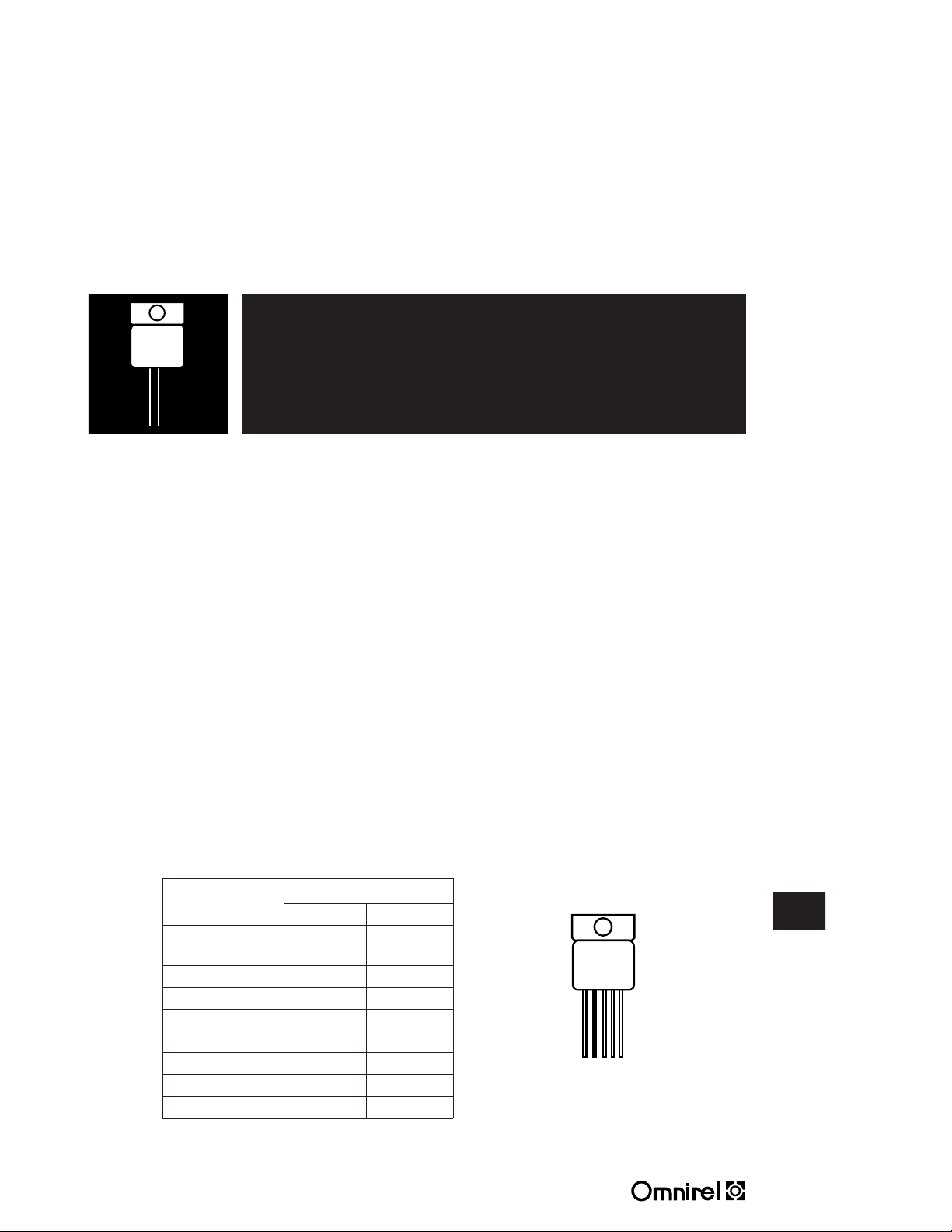
Dual 5V, 12V and 15V, 1.5 Amp Fixed
Voltage Regulators In Single Hermetic
MO-078AA Package
FEATURES
• Positive And Negative Regulators In One Package
• Hermetic 5-Pin Metal Package, JEDEC MO-078AA
• Isolated Case
• Output Voltages 5V, 12V and 15V; Other Voltages Available
• Output Voltages Set Internally To ±2.0%
• Built-In Thermal Overload Protection
• Short Circuit Current Limiting
• Product Is Available Screened To MIL-S-19500, TX, TXV And S Levels
OM7500SC
DESCRIPTION
This series of products offers a positive and a negative fixed voltage regulator in one
hermetically sealed, 5 PIN package whose outline is similar to the industry standard
TO-247 package. With heat sinking, they can regulate over 1.5 Amp of output current
per device. Standard voltages are + or - 5V, 12V and 15V. Other voltages are
available upon request. Output voltages are internally trimmed to ±2.0% of nominal
voltage. These devices are ideally suited for Military applications where small size
and high reliability are required.
To order, use the following Omnirel part numbers to determine the required
output voltage of each regulator within one package.
Omnirel Output Voltages
Part Number Positive Negative
OM7501SC +5V -5V
OM7502SC +5V -12V
OM7503SC +5V -15V
OM7504SC +12V -5V
OM7505SC +12V -12V
OM7506SC +12V -15V
OM7507SC +15V -5V
OM7508SC +15V -12V
OM7509SC +15V -15V
PIN CONNECTION
12345
Pin 1: + Input
Pin 2: + Output
Pin 3: Common
Pin 4: - Input
Pin 5: - Output
3.3
4 11 R4
Supersedes 1 07 R3
3.3 - 121
OM7500SC
INDIVIDUAL POSITIVE REGULATORS
ELECTRICAL CHARACTERISTICS +5 Volt V
Parameter Symbol Test Conditions Min. Max. Unit
Output Voltage V
Line Regulation V
(Note 1)
Load Regulation V
(Note 1)
Standby Current Drain I
Standby Current Drain DI
Change With Line (Line)
Standby Current Drain DI
Change With Load (Load)
Dropout Voltage V
Peak Output Current I
Short Circuit Current I
(Note 2)
Ripple Rejection DV
Output Noise Voltage N
(Note 3) RMS
Long Term Stability DV
(Note 3) Dt
DV
OUT
RLINE
RLOAD
SCD
SCD
SCD
DO
O (pk)
DS
OUT
OUT
IN
O
V
IN
VIN= 7.5V to 20V 5 mV
V
IN
IO = 5mA to 1.5 Amp 12 mV
= 250mA to 750 mA 6 mV
I
O
V
IN
IO= 5mA to 1000mA • 0.5 mA
TA= 25°C, DV
f =120 Hz, DVIN= 10V 66 dB
TA= 25°C, f =10 Hz to 100KHz 40 µV/V
TA= 25°C, t = 1000 hrs. 75 mV
= 10V, Io= 500mA, -55°C TA 125°C (unless otherwise specified)
IN
TA= 25°C 4.92 5.08 V
= 7.5V to 20V • 4.85 5.15 V
• 12 mV
= 8.0V to 12V 4 mV
• 10 mV
• 25 mV
• 15 mV
• 6.5 mA
= 7.5V to 20V • 0.8 mA
= 100mV, I
OUT
= 1.0A 2.5 V
O
TA= 25°C 1.5 3.3 A
VIN= 35V 1.2 A
• 2.8 A
(Note 3) • 60 dB
6mA
3.3
ELECTRICAL CHARACTERISTICS +12 Volt V
= 19V, Io= 500mA, -55°C TA 125°C (unless otherwise specified)
IN
Parameter Symbol Test Conditions Min. Max. Unit
Output Voltage V
Line Regulation V
(Note 1)
OUT
RLINE
TA= 25°C 11.88 12.12 V
= 14.5V to 27V • 11.64 12.36 V
V
IN
VIN= 14.5V to 27V 18 mV
• 50 mV
= 16V to 22V 9 mV
V
IN
• 30 mV
Load Regulation V
(Note 1)
RLOAD
IO = 5mA to 1.5 Amp 32 mV
• 60 mV
= 250mA to 750 mA 20 mV
I
O
• 40 mV
Standby Current Drain I
SCD
6.0 mA
• 6.5 mA
V
Standby Current Drain DI
SCD
Change With Line (Line)
Standby Current Drain DI
SCD
Change With Load (Load)
Dropout Voltage V
Peak Output Current I
Short Circuit Current I
DO
O (pk)
DS
(Note 2)
Ripple Rejection DV
Output Noise Voltage N
IN
DV
OUT
O
(Note 3) RMS
Long Term Stability DV
OUT
(Note 3) Dt
Notes:
1. Load and Line Regulation are specified at a constant junction temperature. Pulse testing with low duty cycle is used.
Changes in output voltage due to heating effects must be taken into account separately.
2. Short Circuit protection is only assured up to V
3. If not tested, shall be guaranteed to the specified limits.
The • denotes the specifications which apply over the full operating temperature range.
= 15V to 30V • 0.8 mA
IN
IO= 5mA to 1000mA • 0.5 mA
DV
= 100mV, I
OUT
= 1.0A • 2.5 V
O
TA= 25°C 1.5 3.3 A
VIN= 35V 1.2 A
• 2.8 A
f =120 Hz, DVIN= 10V 61 dB
(Note 3) • 54 dB
TA= 25°C, f =10 Hz to 100KHz 40 µV/V
TA= 25°C, t = 1000 hrs. 120 mV
= 35V.
IN
3.3 - 122

OM7500SC
ELECTRICAL CHARACTERISTICS +15 Volt V
= 23V, Io= 500mA, -55°C TA 125°C (unless otherwise specified)
IN
Parameter Symbol Test Conditions Min. Max. Unit
Output Voltage V
Line Regulation V
(Note 1)
Load Regulation V
(Note 1) I
Standby Current Drain I
Standby Current Drain DI
Change With Line (Line)
Standby Current Drain DI
Change With Load (Load)
Dropout Voltage V
Peak Output Current I
Short Circuit Current I
(Note 2)
Ripple Rejection DV
Output Noise Voltage N
(Note 3) RMS
Long Term Stability DV
(Note 3) Dt
DV
OUT
RLINE
RLOAD
SCD
SCD
SCD
DO
O (pk)
DS
OUT
OUT
TA= 25°C, DV
IN
O
ELECTRICAL CHARACTERISTICS -5 Volt V
TA= 25°C 14.8 15.2 V
= 18.5V to 30V • 14.6 15.4 V
V
IN
VIN= 17.5V to 30V 20 mV
• 50 mV
= 20V to 26V 15 mV
V
IN
• 25 mV
IO = 5mA to 1.5 Amp 35 mV
= 5mA to 1.0 Amp • 75 mV
O
= 250mA to 750 mA 21 mV
I
O
• 45 mV
6.0 mA
• 6.5 mA
V
= 18.5V to 30V • 0.8 mA
IN
IO= 5mA to 1000mA • 0.5 mA
= 100mV, I
OUT
TA= 25°C 1.5 3.3 A
= 1.0A 2.5 V
O
VIN= 35V 1.2 A
• 2.8 A
f =120 Hz, DVIN= 10V 54 dB
(Note 3) • 52 dB
TA= 25°C, f =10 Hz to 100KHz 40 µV/V
TA= 25°C, t = 1000 hrs. 150 mV
= -10V, Io= 500mA, -55°C TA 125°C (unless otherwise specified)
IN
Parameter Symbol Test Conditions Min. Max. Unit
Output Voltage V
Line Regulation V
(Note 1)
Load Regulation V
(Note 1)
Standby Current Drain I
Standby Current Drain DI
Change With Line (Line)
Standby Current Drain DI
Change With Load (Load)
Dropout Voltage V
Peak Output Current I
Short Circuit Current I
(Note 2)
Ripple Rejection DV
Output Noise Voltage N
(Note 3) RMS
Long Term Stability DV
(Note 3) Dt
Notes:
1. Load and Line Regulation are specified at a constant junction temperature. Pulse testing with low duty cycle is used.
Changes in output voltage due to heating effects must be taken into account separately.
RLOAD
DV
OUT
RLINE
SCD
SCD
SCD
DO
O (pk)
DS
IN
OUT
O
OUT
2. Short Circuit protection is only assured up to V
3. If not tested, shall be guaranteed to the specified limits.
TA= 25°C -4.95 -5.05 V
= -7.5V to -20V • -4.85 -5.15 V
V
IN
VIN= -7.5V to -20V 12 mV
• 25 mV
= -8.0V to -12V 5 mV
V
IN
• 12 mV
IO = 5mA to 1.5 Amp 20 mV
• 25 mV
= 250mA to 750 mA 15 mV
I
O
• 30 mV
2.5 mA
• 3.0 mA
VIN= -7.0V to -20V • 0.4 mA
IO= 5mA to 1000mA • 0.4 mA
DV
= 100mV, I
OUT
= 1.0A • 2.5 V
O
TA= 25°C 1.5 3.3 A
VIN= -35V 1.2 A
• 2.8 A
f =120 Hz, DVIN= -10V 63 dB
(Note 3) • 60 dB
TA= 25°C, f =10 Hz to 100KHz 40 µV/V
TA= 25°C, t = 1000 hrs. 75 mV
=+35V, positive regulator; .VIN= -35V, negative regulator.
IN
The • denotes the specifications which apply over the full operating temperature range.
3.3
3.3 - 123
OM7500SC
3.3
ELECTRICAL CHARACTERISTICS -12 Volt V
= -19V, Io= 500mA, -55°C TA 125°C (unless otherwise specified)
IN
Parameter Symbol Test Conditions Min. Max. Unit
Output Voltage V
Line Regulation V
(Note 1)
OUT
RLINE
TA= 25°C -11.88 -12.12 V
= -14.5V to -27V • -11.64 -12.36 V
V
IN
VIN= -14.5V to -27V 20 mV
• 50 mV
= -16V to -22V 10 mV
V
IN
• 30 mV
Load Regulation V
(Note 1)
RLOAD
IO = 5mA to 1.5 Amp 32 mV
• 60 mV
= 250mA to 750 mA 16 mV
I
O
• 30 mV
Standby Current Drain I
SCD
3.5 mA
• 4.0 mA
Standby Current Drain DI
SCD
Change With Line (Line)
Standby Current Drain DI
SCD
Change With Load (Load)
Dropout Voltage V
Peak Output Current I
Short Circuit Current I
DO
O (pk)
DS
(Note 2)
Ripple Rejection DV
Output Noise Voltage N
IN
DV
OUT
O
(Note 3) RMS
Long Term Stability DV
OUT
(Note 3) Dt
ELECTRICAL CHARACTERISTICS -15 Volt V
Parameter Symbol Test Conditions Min. Max. Unit
Output Voltage V
Line Regulation V
(Note 1)
OUT
RLINE
VIN= -14.5V to -27V • 0.8 mA
IO= 5mA to 1000mA • 0.5 mA
DV
= 100mV, I
OUT
= 1.0A • 1.8 V
O
TA= 25°C, IO= 5mA to 1A 1.5 3.3 A
V
= -35V 1.2 A
IN
• 2.8 A
f =120 Hz, DVIN= -10V 56 dB
(Note 3) • 53 dB
TA= 25°C, f =10 Hz to 100KHz 40 µV/V
TA= 25°C, t = 1000 hrs. 120 mV
= -23V, Io= 500mA, -55°C TA 125°C (unless otherwise specified)
IN
TA= 25°C -14.85 -15.15 V
= -17.5V to -30V • -14.55 -15.45 V
V
IN
VIN= -17.5V to -30V 25 mV
• 50 mV
= -20V to -26V 15 mV
V
IN
• 25 mV
Load Regulation V
(Note 1)
RLOAD
IO = 5mA to 1.5 Amp 35 mV
• 75 mV
= 250mA to 750 mA 21 mV
I
O
• 45 mV
Standby Current Drain I
SCD
6.0 mA
• 6.5 mA
Standby Current Drain DI
SCD
Change With Line (Line)
Standby Current Drain DI
SCD
Change With Load (Load)
Dropout Voltage V
Peak Output Current I
Short Circuit Current I
DO
O (pk)
DS
(Note 2)
Ripple Rejection DV
Output Noise Voltage N
IN
DV
OUT
O
(Note 3) RMS
Long Term Stability DV
OUT
(Note 3) Dt
Notes:
1. Load and Line Regulation are specified at a constant junction temperature. Pulse testing with low duty cycle is used.
Changes in output voltage due to heating effects must be taken into account separately.
2. Short Circuit protection is only assured up to V
3. If not tested, shall be guaranteed to the specified limits.
The • denotes the specifications which apply over the full operating temperature range.
VIN= -17.5V to -30V • 0.8 mA
IO= 5mA to 1000mA • 0.5 mA
DV
= 100mV, I
OUT
= 1.0A • 2.5 V
O
TA= 25°C 1.5 3.3 A
VIN= -35V 1.2 A
• 2.8 A
f =120 Hz, DVIN= -10V 53 dB
(Note 3) • 50 dB
TA= 25°C, f =10 Hz to 100KHz 40 µV/V
TA= 25°C, t = 1000 hrs. 150 mV
= -35V.
IN
3.3 - 124
OM7500SC
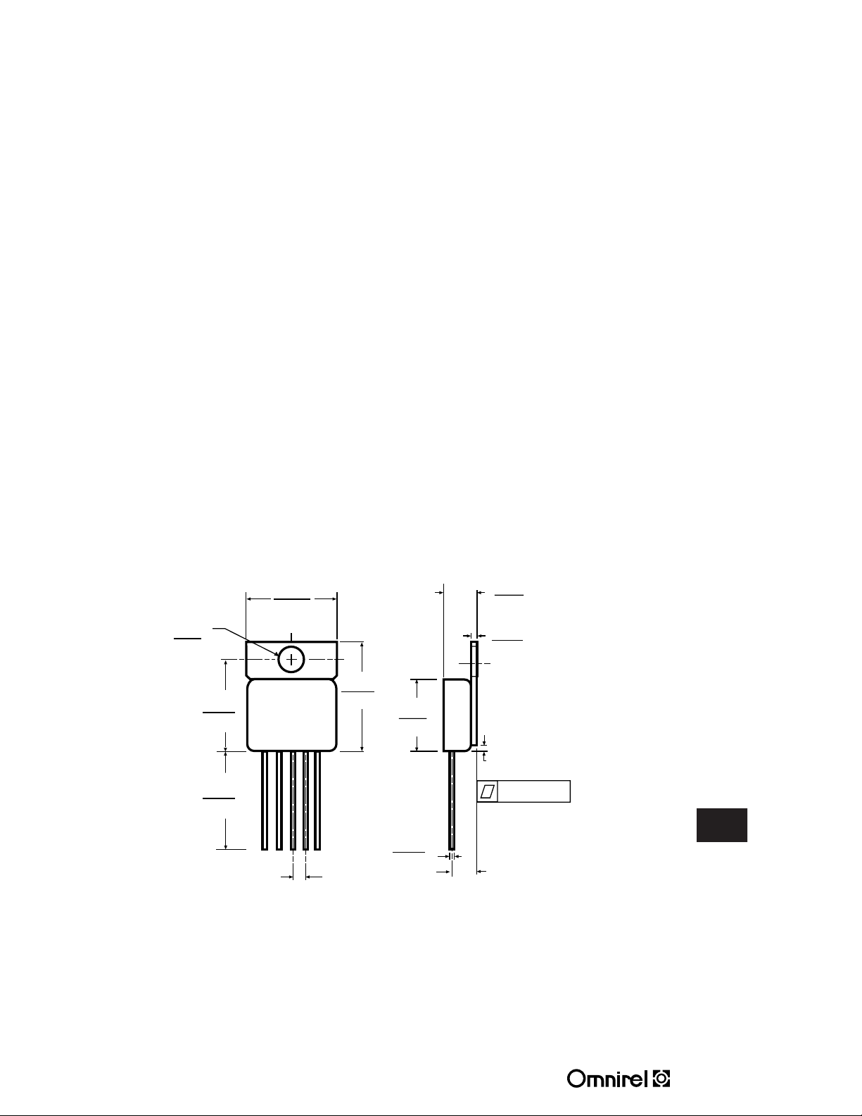
.100
TYP.
.140 TYP.
.035
.025
.707
.697
.750
.500
.835
.815
.695
.685
.165
.155
.550
.530
.270
.240
.045
.035
.092 MAX.
.005
ABSOLUTE MAXIMUM RATINGS (Per Regulator)
Input Voltage ........................Positive Regulator = 35V, Negative Regulator = - 35V
Operating Junction Temperature Range..................................-55°C to +150°C
Storage Temperature Range ...........................................-65°C to +150°C
Typical Power/Thermal Characteristics
Rated Power @ 25°C
TC....................................................................17.5W
TA.......................................................................3W
Thermal Resistance
qJC..................................................................4.2°C/W
qJA...................................................................42°C/W
Thermal Shutdown, IO= 5mA, VIN@ Voltage ......................................175°C
MECHANICAL OUTLINE
NOTES:
• Case is metal/hermetically sealed
• Isolated Tab
3.3 - 125
3.3
 Loading...