

Page 1

H. DESCRIPTION OF MECHANISM
C-700 Ultra Zoom
H. DESCRIPTION OF MECHANISM
[1] CA1 CIRCUIT DESCRIPTION ................................................................................ H-2
[2] CA2 CIRCUIT DESCRIPTION ................................................................................ H-5
[3] ST1 POWER CIRCUIT DESCRIPTION ..................................................................H-7
[4] ST1 STROBE CIRCUIT DESCRIPTION................................................................. H-8
[5] SYA CIRCUIT DESCRIPTION ................................................................................ H-9
H-1 Ver.1
Page 2
H. DESCRIPTION OF MECHANISM C-700 Ultra Zoom
[1] CA1 CIRCUIT DESCRIPTION
1. IC Configuration
IC903 (ICX284AK) CCD imager
IC902 (74ACT04MTC) H driver
IC904 (CXD3400N) V driver
IC905 (AD9806) CDS, AGC, A/D converter
2. IC903 (CCD)
[Structure]
Interline type CCD image sensor
Optical size 1/2.7 type
Effective pixels 1636 (H) X 1236 (V)
Pixels in total 1688 (H) X 1248 (V)
Optical black
Horizontal (H) direction: Front 4 pixels, Rear 48 pixels
Vertical (V) direction: Front 10 pixels, Rear 2 pixels
Dummy bit number Horizontal : 28 Vertical :1
(only even number field)
Pin 1
2
3A
φ
V
1
φ
H
4
φ
V
1
(Note)
16
2
φ
H
1B
φ
OUT
V
7
8
9
10
DD
V
φ
V
GND
6
Ye
Ye
Ye
Vertical register
11
SUB
GND
φ
V
4
5
Cy
G
Mg
Cy
Mg
G
Cy
G
Mg
Horizontal register
13
12
SUB
C
(Note) : Photo sensor
φ
φ
V
V
3
2
Ye
Cy
G
Mg
Ye
Cy
G
Mg
Ye
Cy
G
Mg
14
RG
φ
15
L
V
3B
2
1A
V
4
Pin 11
H
48
Fig. 1-1.Optical Black Location (Top View)
Pin No.
1
2, 3
4
5, 6
7, 10
8
9
11
12
13
14
15
16
Symbol
V
φ
V
3A, Vφ3B
V
φ
V
1A, Vφ1B
GND
OUT
V
VDD
φ
SUB
SUB
C
VL
φ
RG
H
H
φ
Vertical register transfer clock
4
Vertical register transfer clock
φ
Vertical register transfer clock
2
Vertical register transfer clock
GND
Signal output
Circuit power
Substrate clock
Substrate bias
Protection transistor bias DC
Reset gate clock
φ
Horizontal register transfer clock
1
φ
Horizontal register transfer clock
2
Pin Description
10
Fig. 1-2. CCD Block Diagram
Waveform
GND 0 V
DC
DC
DC
Voltage
-7.5 V, 0 V
-7.5 V, 0 V, 15 V
-7.5 V, 0 V
-7.5 V, 0 V, 15 V
Aprox. 10 V
15 V
Aprox. 8 V
Aprox. 8V
(Different from every CCD)
12.5 V, 16 V
0 V, 3.3 V
0 V, 3.3 V
Table 1-1. CCD Pin Description
H-2 Ver. 1
When sensor read-out
Page 3
H. DESCRIPTION OF MECHANISMC-700 Ultra Zoom
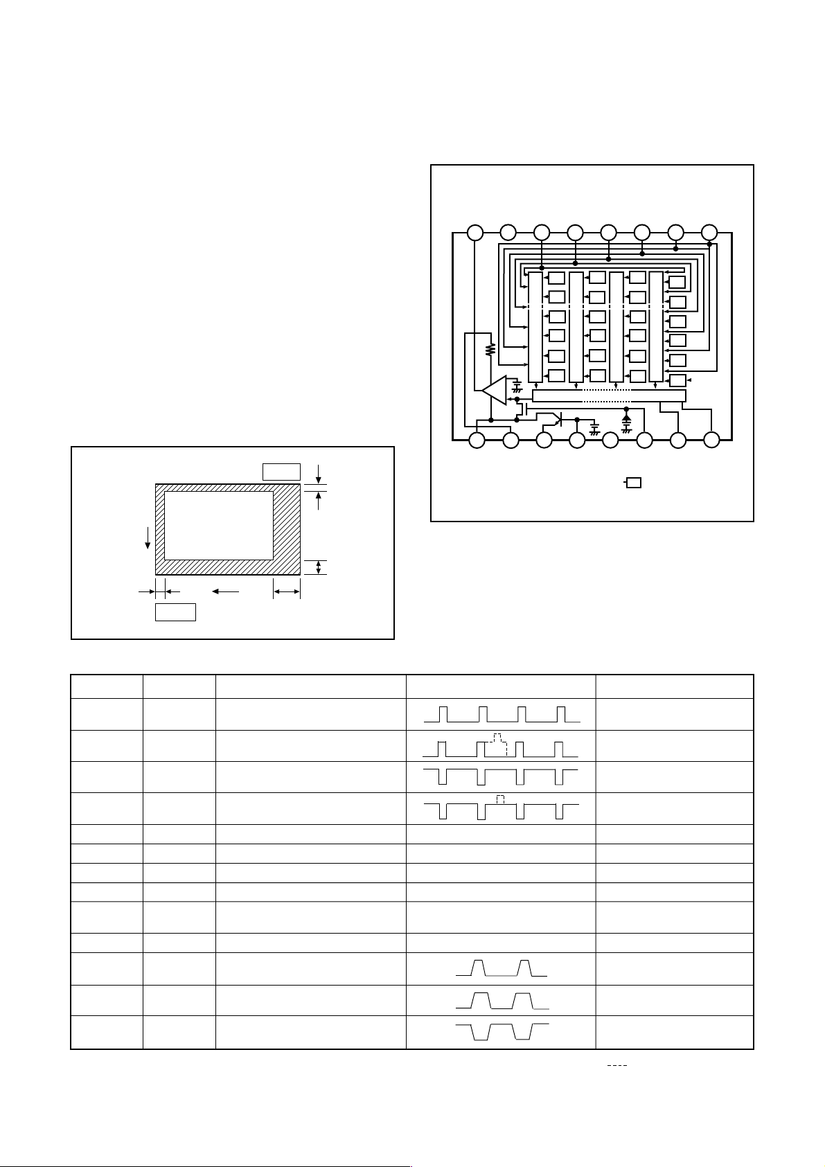
3. IC902 (H Driver) and IC904 (V Driver)
An H driver (IC902) and V driver (IC904) are necessary in
order to generate the clocks (vertical transfer clock, horizontal transfer clock and electronic shutter clock) which
driver the CCD.
IC902 is an inverter IC which drives the horizontal CCDs
(H1 and H2). In addition the XV1-XV4 signals which are
output from IC102 are the vertical transfer clocks, and the
XSG1 and XSG signal which is output from IC102 is superimposed onto XV1 and XV3 at IC904 in order to generate a
ternary pulse. In addition, the XSUB signal which is output
from IC102 is used as the sweep pulse for the electronic
shutter, and the RG signal which is output from IC102 is
the reset gate clock.
14
CC
1A
1Y
2A
2Y
3A
1
2
3
4
5
V
13
6A
12
6Y
11
5A
10
5Y
4. IC905 (CDS, AGC Circuit and A/D Converter)
The video signal which is output from the CCD is input to
Pins (26) and (27) of IC905. There are S/H blocks inside
IC905 generated from the XSHP and XSHD pulses, and it
is here that CDS (correlated double sampling) is carried
out.
After passing through the CDS circuit, the signal passes
through the AGC amplifier. It is A/C converted internally
into a 10-bit signal, and is then input to IC102 of the CA2
circuit board.
CCDIN
CLPDM
DAC1
DAC2
PBLK
0-34 dB
CDS
CLAMP
8B DAC
8B DAC
PGA
10B DAC
INTF
3
3-W INTF ADCIN
Fig. 1-5. IC905 Block Diagram
MUX
PGA
AUXIN
CLP B
CLP
S/H
0-15 dB
CLAMP
AD9806
ADC
REF
TIMING
GENERAT R
SHD
ADCCLK
SHP
10
DOUT
VRT
VRB
6
3Y
7
GND
Fig. 1-3. IC902 Block Diagram
V
DD
1
Input
Buffer
2
3
4
5
6
7
8
9
10
XSHT
XV3
XSG3B
XSG3A
XV1
XSG1B
XSG1A
XV4
XV2
9
8
SHT
V3B
V
V3A
V1B
V
V1A
V4
V2
GND
4A
4Y
20
19
L
18
17
16
H
15
14
13
12
11
Ver. 1
Fig. 1-4. IC904 Block Diagram
H-3
Page 4
H. DESCRIPTION OF MECHANISM C-700 Ultra Zoom
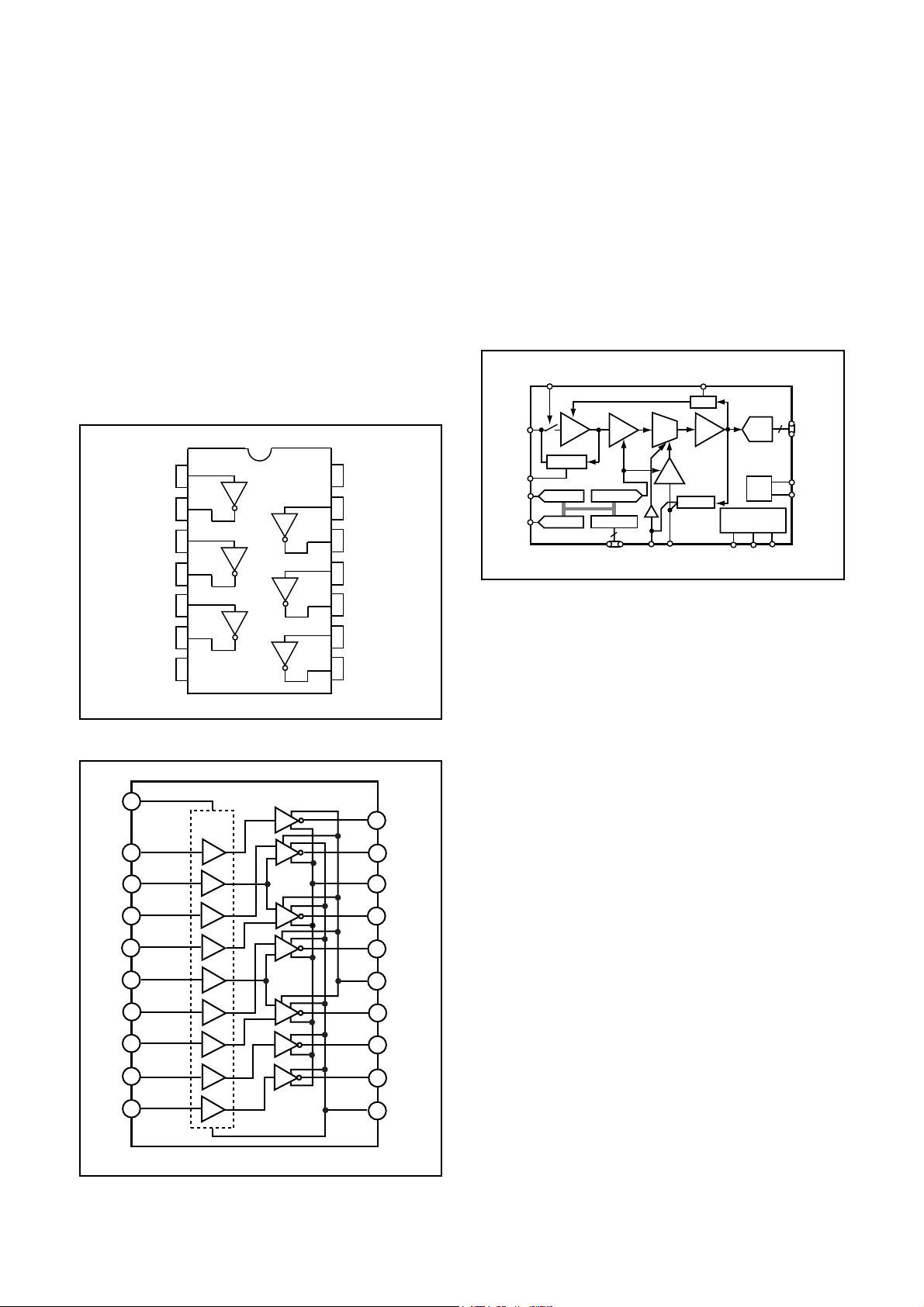
5. Transfer of Electric Charge by the Horizontal CCD
The transfer system for the horizontal CCD emplays a 2-phase drive method.
The electric charges sent to the final stage of the horizontal CCD are transferred to the floating diffusion, as shown in Fig. 1-
6. RG is turned on by the timing in (1), and the floating diffusion is charged to the potential of PD. The RG is turned off by the
timing in (2). In this condition, the floating diffusion is floated at high impedance. The H1 potential becomes shallow by the
timing in (3), and the electric charge now moves to the floating diffusion.
Here, the electric charges are converted into voltages at the rate of V = Q/C by the equivalent capacitance C of the floating
diffusion. RG is then turned on again by the timing in (1) when the H1 potential becomes deep.
Thus, the potential of the floating diffusion changes in proportion to the quantity of transferred electric charge, and becomes
CCD output after being received by the source follower. The equivalent circuit for the output circuit is shown in Fig. 1-7.
(1)
H1 H2 H1 H2 H1 HOG RG
CCD OUT
Floating diffusion
(2)
H1 H2 H1 H2 H1 HOG RG
PD
H1
H2
CCD OUT
PD
RG
(1) (2) (3)
3.5V
0V
3.5V
0V
13.5V
0V
(3)
H1 H2 H1 H2 H1 HOG RG
Reset gate pulse
Direction of transfer
H Register
Electric
charge
Floating diffusion gate is
floated at a high impedance.
CCD OUT
CCD OUT
Fig. 1-6. Horizontal Transfer of CCD Imager and Extraction of Signal Voltage
The shutter hold signal(VCTRL) which is output from the
12V Pre-charge drain bias (PD)
ASIC (IC102) is restricted the shutter electric current. (maintenance electric current)
6-2. Iris drive
The iris stepping motor drive signals (ACTRL1, ACTRL2,
ACTRL3 and ACTRL4) which are output from the ASIC
(IC102) are used to drive by the motor driver (IC954). Detection of the standard iris positions is carried out by means
Voltage output
of the photointerruptor (PI2) inside the lens block.
6-3. Focus drive
The focus stepping motor drive signals (LDIN1, LDIN2, LDIN3
C is charged
equivalently
and LDIN4) which are output from the ASIC expansion port
(IC107) are used to drive by the motor driver (IC953). Detection of the standard focusing positions is carried out by
means of the photointerruptor (PI) inside the lens block.
RG pulse leak signal
Signal voltage
Black level
Fig. 1-7. Theory of Signal Extraction Operation
6. Lens drive block
6-1. Shutter drive
The shutter drive signal (PCTRL) which is output from the
ASIC expansion port (IC106) is drived the shutter constant
level driver, and then shutter plunger is opened and closed.
6-4. Zoom drive
The zoom stepping motor drive signals (ZIN1, ZIN2, ZIN3
and ZIN4) which are output from the ASIC expansion port
(IC107) are used to drive by the motor driver (IC953). Detection of the zoom positions is carried out by means of
photoreflector (PR1 and PR2) inside the lens block.
H-4 Ver. 1
Page 5

H. DESCRIPTION OF MECHANISMC-700 Ultra Zoom
[2] CA2 CIRCUIT DESCRIPTION
1. Circuit description
1-1. Digital clamp
The optical black section of the CCD extracts averaged values from the subsequent data to make the black level of
the CCD output data uniform for each line. The optical black
section of the CCD averaged value for each line is taken
as the sum of the value for the previous line multiplied by
the coefficient k and the value for the current line multiplied
by the coefficient 1-k.
1-2. Signal processor
γγ
1.
γ correction circuit
γγ
This circuit performs (gamma) correction in order to maintain a linear relationship between the light input to the camera and the light output from the picture screen.
2. Color generation circuit
This circuit converts the CCD data into RGB signals.
3. Matrix circuit
This circuit generates the Y signals, R-Y signals and B-Y
signals from the RGB signals.
4. Horizontal and vertical aperture circuit
This circuit is used gemerate the aperture signal.
1-3. AE/AWB and AF computing circuit
The AE/AWB carries out computation based on a 64-segment screen, and the AF carries out computations based
on a 6-segment screen.
1-4. SDRAM controller
This circuit outputs address, RAS, CAS and AS data for
controlling the SDRAM. It also refreshes the SDRAM.
1-5. SIO
This is the interface for the 8-bit microprocessor.
1-6. PIO/PWM/SIO for LCD
8-bit parallel input and output makes it possible to switch
between individual input/output and PWM input/output.
1-7. TG/SG
Timing generated for 2 million pixel CCD control.
1-8. Digital encorder
It generates chroma signal from color difference signal.
2. Outline of Operation
When the shutter opens, the reset signals (ASIC and CPU)
and the serial signals (“take a picture” commands) from
the 8-bit microprocessor are input and operation starts.
When the TG/SG drives the CCD, picture data passes
through the A/D and CDS, and is then input to the ASIC as
10-bit data.
The AF, AE, AWB, shutter, and AGC value are computed
from this data, and three exposures are made to obtain the
optimum picture. The data which has already been
stored in the SDRAM is read by the CPU and color generation is carried out. Each pixel is interpolated from the surrounding data as being either Ye, Cy, Mg or B primary color
data to produce R, G and B data. At this time, correction of
the lens distortion which is a characteristic of wide-angle
lenses is carried out. After AWB and γ processing are carried out, a matrix is generated and aperture correction is
carried out for the Y signal, and the data is then compressed by JPEG and is then written to card memory (smart
media).
When the data is to be output to an external device, it is
taken data from the memory and output via the USART.
When played back on the LCD and monitor, data is transferred from memery to the SDRAM, and the image is then
elongated so that it is displayed over the SDRAM display
area.
3. LCD Block
During monitoring, YUV conversion is carried out for the
10-bit CCD data which is input from the A/D conversion
block to the ASIC and is then transferred to the SDRAM so
that the CCD data can be displayed on the LCD.
The data which has accumulated in the SDRAM is passed
through the NTSC encoder , and after D/A conversion is
carried out to change the data into a Y/C signal, the data is
sent to the LCD panel and displayed.
If the shutter button is pressed in this condition, the 10-bit
data which is output from the A/D conversion block of the
CCD is sent to the SDRAM (DMA transfer), and after processor, it is displayed on the LCD as a freeze-frame image.
During playback, the JPEG image data which has accumulated in the flash memory is converted to YUV signals, and
then in the same way as during monitoring, it is passed
through the NTSC endoder, and after D/A conversion is
carried out to change the data into a Y/C signal, the data is
sent to the LCD panel and displayed.
The two analog signal (Y/C signals) from the ASIC are converted into RGB signals by the LCD driver, and these RGB
signals and the control signal which is output by the LCD
driver are used to drive the LCD panel. The RGB signals
are 1H transposed so that no DC component is present in
the LCD element, and the two horizontal shift register clocks
drive the horizontal shift registers inside the LCD panel so
that the 1H transposed RGB signals are applied to the LCD
panel. Because the LCD closes more as the difference in
potential between the COM (common polar voltage: fixed
at DC) and the R, G and B signals becomes greater, the
display becomes darker; if the difference in potential is
smaller, the element opens and the LCD become brighter.
Ver. 1
H-5
Page 6

H. DESCRIPTION OF MECHANISM C-700 Ultra Zoom
CP1 (CAA) CIRCUIT WAVEFORMS
TEST
LOCATION
WAVEFORM
TEST
LOCATION
WAVEFORM
IC101
PIN 61
ZAS
1V/div
2µs/div
IC101
PIN 132
CLKIN
1V/div
20ns/div
IC111
PIN 1
REFCLK
1V/div
20ns/div
IC111
PIN 9
CLKOUT
1V/div
20µs/div
IC172
PIN 18
STH1
2V/div
20µs/div
H-6
Ver. 1
Page 7

H. DESCRIPTION OF MECHANISMC-700 Ultra Zoom
[3] ST1 POWER CIRCUIT DESCRIPTION
1. Outline
This is the main power circuit, and is comprised of the following blocks.
Switching controller (IC501)
Digital 5.1 V and analog system power output (T5001,
Q5001)
Digital 2.55 V system power supply (Q5010)
Digital 3.35 V system power supply (Q5009)
LCD system power supply (Q5010, T5002)
LCD Backlight power supply output (Q5013)
EVF Backlight power supply output (Q5019)
2. Switching Controller (IC501)
This is the basic circuit which is necessary for controlling
the power supply for a PWM-type switching regulator, and
is provided with four five-in channels, only CH2 (digital 5.1
V, analog system), CH4 (LCD system), CH3 (digital 3.35
V), CH1 (LCD backlight) and CH5 (EVF backlight) are used.
Feedback from 5.1 V (D) (CH2), 12.4 V (L) (CH4) and 3.35
V (D) (CH3) power supply outputs are received, and the
PWM duty is varied so that each one is maintained at the
correct voltage setting level. LCD backlight (CH1) and EVF
backlight (CH5) provide feedback on the voltages at both
ends of the resistors, so that constant current control can
be carried out in order to maintain the current at the setting
level.
2-1. Short-circuit protection circuit
If output is short-circuited for the length of time determined
by the condenser which is connected to Pin (29) of IC501,
all output is turned off. The control signal (P ON, P(A) ON,
LCD ON, LCD BL and EVF BL) are recontrolled to restore
output.
3. Digital 5.1 V and Analog System Power Output
5.1 V (D) , 15.0 V (A), -7.6 V (A) and 5.0 V (A) are output.
Feedback for the 5.1 V (D) is provided to the switching controller (Pins (35) of IC501) so that PWM control can be carried out.
4. Digital 2.55 V System Power Output
2.55 V (D) is output. It is created from the digital 3.55 V by
means of series regulator control which is carried out by
IC502 and Q5010.
5. Digital 3.35 V System Power Output
3.35 V (D) is output. Feedback is provided to the swiching
controller (Pin (23) of IC501) so that PWM control can be
carried out.
6. LCD System Power Output
12.4 V (L) and 3.7 V (L) are output. Feedback for the 12.4
V (L) is provided to the switching controller (Pin (22) of
IC501) so that PWM control can be carried out.
7. LCD Backlight Power Supply Output
A constant current (15 mA) flows to the LCD backlight LEDs.
The voltages at both ends of the resistor which is connected
in series to the LEDs is sent to the switching controller (pin
(41) of IC501) for feedback so that PWM control is carried
out.
8. EVF Backlight Power Supply Output
A constant current (15 mA) flows to the EVF backlight LEDs.
The voltages at both ends of the resistor which is connected
in series to the LEDs is sent to the switching controller (pin
(17) of IC501) for feedback so that PWM control is carried
out.
Ver. 1
H-7
Page 8

H. DESCRIPTION OF MECHANISM C-700 Ultra Zoom
[4] ST1 STROBE CIRCUIT DESCRIPTION
1. Charging Circuit
When UNREG power is supplied to the charge circuit and
the CHG signal from SYA circuit on the CP1 board becomes
High (3.3 V), the charging circuit starts operating and the
main electorolytic capacitor is charged with high-voltage
direct current.
However, when the CHG signal is Low (0 V), the charging
circuit does not operate.
1-1. Power switch
When the CHG signal switches to Hi, Q5406 turns ON and
the charging circuit starts operating.
1-2. Power supply filter
L5401 and C5401 constitute the power supply filter. They
smooth out ripples in the current which accompany the
switching of the oscillation transformer.
1-3. Oscillation circuit
This circuit generates an AC voltage (pulse) in order to increase the UNREG power supply voltage when drops in
current occur. This circuit generates a drive pulse with a
frequency of approximately 50-100 kHz. Because self-excited light omission is used, the oscillation frequency
changes according to the drive conditions.
2. Light Emission Circuit
When RDY and TRIG signals are input from the ASIC expansion port, the stroboscope emits light.
2-1. Emission control circuit
When the RDY signal is input to the emission control circuit, Q5409 switches on and preparation is made to let current flow to the light emitting element. Moreover, when a
STOP signal is input, the stroboscope stops emitting light.
2-2. Trigger circuit
When a TRIG signal is input to the trigger circuit, D5405
switches on, a high-voltage pulse of several kilovolts is generated inside the trigger circuit, and this pulse is then applied to the light emitting part.
2-3. Light emitting element
When the high-voltage pulse form the trigger circuit is applied to the light emitting part, currnet flows to the light emitting element and light is emitted.
Beware of electric shocks.
1-4. Oscillation transformer
The low-voltage alternating current which is generated by
the oscillation control circuit is converted to a high-voltage
alternating current by the oscillation transformer.
1-5. Rectifier circuit
The high-voltage alternating current which is generated at
the secondary side of T5401 is rectified to produce a highvoltage direct current and is accumulated at electrolytic capacitor C5412 on the main circuit board.
1-6. Voltage monitoring circuit
This circuit is used to maintain the voltage accumulated at
C5412 at a constance level.
After the charging voltage is divided and converted to a
lower voltage by R5417 and R5419, it is output to the SYA
circuit on the CP1 board as the monitoring voltage VMONIT.
When this VMONIT voltage reaches a specified level at the
SYA circuit on the CP1 board, the CHG signal is switched
to Low and charging is interrupted.
H-8 Ver. 1
Page 9

H. DESCRIPTION OF MECHANISMC-700 Ultra Zoom
[5] SYA CIRCUIT DESCRIPTION
1. Configuration and Functions
For the overall configuration of the SYA circuit, refer to the block diagram. The configuration of the SYA circuit centers around
a 8-bit microprocessor (IC301).
The 8-bit microprocessor handles the following functions.
1. Operation key input, 2. Clock control, 3. Power ON/OFF, 4. Storobe charge control
Pin
1~4
5
6
7
8
9
10
11
12
13
14
15
16
17
18
19
20
21
22
23
24 VDD
25 AVSS
26~29 SCAN IN 0~3
30~31
32
33
34
35
36
37
38
39
40
41
42
43
44
45
46
47
48
Ver. 1
Signal
SCAN OUT 0~3
P ON
PA ON
LCD ON
LCD BL
VSS
VDD
LED 0 (SELF LED)
LED 1 (CARD LED)
NOT USED
AVREF ON
SI
SO
SCK
PRG SI
PRG SO
PRG SCK
AV JACK
NOT USED
CHG ON
NOT USED
CHG VOL
BATTERY
AVREF
AVDD
RESET
XCOUT
XCIN
IC
XOUT
XIN
VSS
BAT OFF
SREQ
STR CONNECT
POWER ON
PMUTE ON
MUTE ON/OFF
I/O
O
O
O
O
O
O
O
O
O
O
O
O
O
O
O
O
O
Outline
Key matrix output
DC/DC converter ON/OFF signal H : ON
DC/DC converter (analog) ON/OFF signal H : ON
LCD monitor power ON/OFF signal H : ON
LCD backlight ON/OFF signal H : ON
-
-
-
I
I
I
-
-
-
I
-
I
I
I
-
I
I
-
I
-
I
I
I
I
GND
Power supply terminal
Self timer LED ON/OFF signal L : LED lighting
Card LED ON/OFF signal L : LED lighting
-
A/D standard voltage ON/OFF signal L : ON
Serial communication data input (←ASIC)
Serial communication data input (→ASIC)
Serial communication clock output
Flash rewrite serial communication data input
Flash rewrite serial communication data output
Flash rewrite serial communication clock output
Video output cable connection detection signal L : Connection
-
Flash charge ON/OFF signal H : ON
Power supply termianl
A/D converter GND power terminal
Key matrix input
-
Storobe charge voltage input (analog input)
Battery voltage input
A/D converter standard voltage input terminal
A/D converter analog power terminal
Reset input
Sub clock oscillation terminal (32.768 kHz)
Sub clock oscillation terminal
Connect to VSS
Main clock oscillation terminal (4MHz)
Main clock oscillation terminal
GND
Battery off detection signal
Serial communication requirement signal L : Requirement
External storobe signal detection
Power switch detection terminal (interruption)
Mute IC power ON/OFF signal
Mute ON/OFF signal
H-9
Page 10

H. DESCRIPTION OF MECHANISM C-700 Ultra Zoom
49
50
51
52
53~56
57
58~59
60
61
62
63
64
COM REQ I ASIC serial communication requirement
DC IN
CARD
BUZZER
SCAN IN 4~7
USB
NOT USED
EVF BL
NOT USED
ASIC TEST
ASIC RESET
MAIN RESET
I DC power detection terminal L : Requirement
I
O
I
I
-
O
-
O
O
O
Table 4-1. 8-bit Microprocessor Port Specification
Expansion memory card attachment detection signal L : Attachment
Buzzer output signal (4 kHz)
Key matrix input
USB cable connection detection signal
-
EVF back light ON/OFF signal
-
ASIC reset control signal
ASIC reset signal
SPARC reset signal
2. Internal Communication Bus
The SYA circuit board carries out overall control of camera operation by detecting the input from the keyboard and the
condition of the camera circuits. The 8-bit microprocessor reads the signals from each sensor element as input data and
outputs this data to the camera circuits (ASIC) or to the LCD display device as operation mode setting data. Fig. 4-1 shows
the internal communication between the 8-bit microprocessor, ASIC and SPARC lite circuits.
RESET
SREQ
8-bit
Microprocessor
ASIC SO
ASIC
ASIC SI
ASIC SCK
RESET
Fig. 4-1 Internal Bus Communication System
3. Key Operaiton
For details of the key operation, refer to the instruction manual.
SCAN
SCAN
OUT
IN
0
1
2
0
SEQUENTIAL
SHOT
Z D1
J UP
1
A/M/S
Z D2
J DOWN
23
P
Z UP2
J LEFT
FULL AUTO
Z UP1
J RIGHT
DATA BUS
4
PORTRAIT SPORTS
1 st
5
2nd
32-bit
SPARC lite
6
SOUVENIR
PICTURE
POP UP SW
P ON
7
PLAY
TEST
3
FLASH
SPOT/MACRO
DRIVE
Table 4-2. Key Operation
LCD
H-10
AEL/CUSTOM
OK
CARD SW
Ver. 1
Page 11

H. DESCRIPTION OF MECHANISMC-700 Ultra Zoom
4. Power Supply Control
The 8-bit microprocessor controls the power supply for the overall system.
The following is a description of how the power supply is turned on and off. When the battery is attached, a regulated 3.2 V
voltage is normally input to the 8-bit microprocessor (IC301) by IC302, so that clock counting and key scanning is carried out
even when the power switch is turned off, so that the camera can start up again. When the battery is removed, the 8-bit
microprocessor operates in sleep mode using the backup capacitor. At this time, the 8-bit microprocessor only carries out
clock counting, and waits in standby for the battery to be attached again. When a switch is operated, the 4-bit microprocessor supplies power to the system as required.
The 8-bit microprocessor first sets both the P ON signal at pin (5) and the PA ON signal at pin (6) to high, and then turns on
the DC/DC converter. After this, High signals are output from pins (63) and (64) so that the ASIC and the SPARC lite are set
to the active condition. If the LCD monitor is on, the LCD ON signal at pin (7) set to high, the DC/DC converter for the LCD
monitor is turned on, and is controlled backlight both the LCD BL signal at pin (8) and the EVF BL signal at pin (60). Once
SPARC lite processing is completed, the ASIC and the SPARC lite return to the reset condition, all DC/DC converters are
turned off and the power supply to the whole system is halted.
Power
ON
Supply voltage
Power OFF
Play back
Power switch ON-
Auto power down
Shutter switch ON
Resolution, Flash,
Self timer switch ON
LCD finder
Supply voltage
SPARC
Lite
3.3 V, 2.5 V
OFF
ON
OFF
ON
OFF
ON
Table 4-3. Camera Mode (Battery Operation)
SPARC
Lite
3.3 V 3.3 V
ASIC,
memory
3.3 V, 2.5 V
OFF
ON
OFF
ON
OFF
ON
ASIC,
memory
CCD
5 V (A)
+15 V -9 V
OFF
OFF
OFF
ON→OFF
OFF
ON
CCD
5 V (A)
+15 V -9 V
4bit
CPU
3.2 V
(ALWAYS)
32KHz OFF
4MHz ON
4MHz ON
4MHz ON
4MHz ON
4MHz ON
4bit
CPU
3.2 V
(ALWAYS)
MODE
(ALWAYS)
MODE
(ALWAYS)
LCD
3.2 V
LCD
3.2 V
LCD
MONITOR
5V (L)
+12V etc.
OFF
ON
OFF
OFF
OFF
ON
LCD
MONITOR
5 V (L)
+12V etc.
Power OFF
Power switch ON-
Auto power down
Take a picture
Erase image
Power
Download image
ON
Continuous image
Message from host
Note) P. SAVE = Power save mode, 4 MHz = Main clock operation, 32 kHz = Sub clock operation
Table 4-4. Host Mode (Battery Operation)
Ver. 1
OFF OFF
OFF OFF
ON ON
ON ON
ON
ON
ON
ON
ON
ON
H-11
OFF
OFF
ON→OFF
OFF
OFF
ON
ON
32 KHz OFF OFF
4 MHz ON OFF
4 MHz ON OFF
4 MHz ON OFF
4 MHz ON OFF
4 MHz ON OFF
4 MHz ON OFF
 Loading...