

Page 1

H. DESCRIPTION OF MECHANISM X-450/C-370/D-535
H. DESCRIPTION OF MECHANISM
[1] CIRCUIT OPERATION DESCRIPTION…………………….. H-2
1. SUBSTRATE COMPOSITION…………………………….H-2
2. POWER SUPPLY COMPOSITION……………………….H-3
[2] DESCRIPTION OF EACH SUBSTRATE.…………………... H-4
1. FLASH BOARD……………………………………………. H-4
2. POWER BLOCK…………………………………………... H-7
3. CCD BOARD………………………………………………. H-7
4. MCU BLOCK………………………………………………. H-11
H-1
Page 2
H. DESCRIPTION OF MECHANISM X-450/C-370/D-535
[1] Circuit Operation Description
1. Substrate Composition
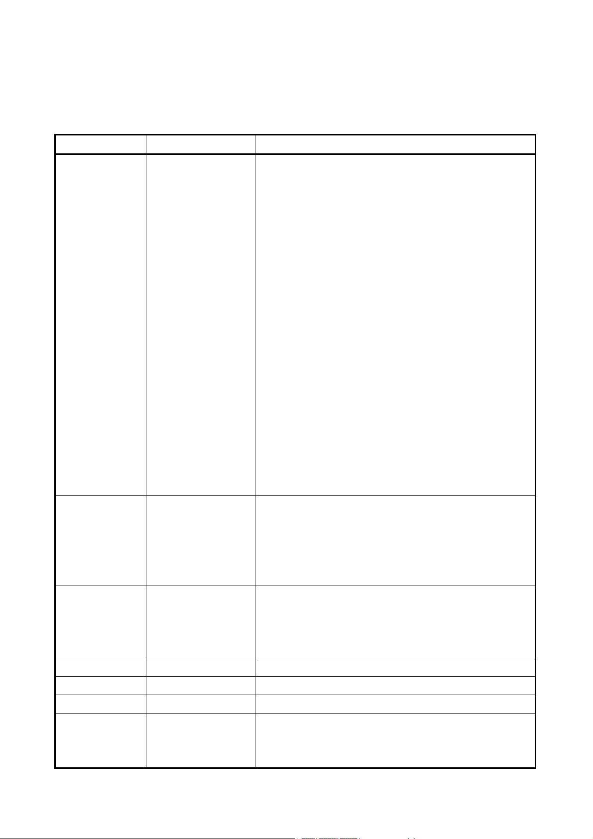
Parts number Name Description
9J737-001 MCU BOARD U2: DSP ZORAN COACH 6 (SYSTEM CONTROL,
IMAGE PROCESS, AMBIENT I/F & RTC)
U4: MOTOR DRIVE M50234FP (LENS DRIVE)
U5: INTERNAL 16MB FLASH MEMORY K9F2808
(DSP CORE & BUILD-IN IMAGE DATA)
U6: 6 CHANNEL POWER MANAGEMENT MAX156
7ETL
U7: 128Mb SDRAM IC42S16800-7T
J2: TO FLASH BOARD CONNECTOR
J3: TO LENS FPC CONNECTOR
J4: DC 3.4V JACK
J5: USB JACK
JP1: TO CCD BOARD CONNECTOR
JP2: TO TOP FPC CONNECTOR
J401: TO LCD PANEL CONNECTOR
JC1: TV JACK
JC2: XD CONNECTOR
9J737-501 CCD BOARD U1: 3.34M PIXEL CCD SENSOR MN39480PJG
U3: 25MSPS CORRELATED DOUBLE SAMPLER
AD9943
U5: VERTICAL DRIVE AN20101A
U6: TIMING GENERATOR MN52B6CH
9J737-401 FLASH BOARD U400: FLASH CAPACITOR CHARGER IC AT1452
U401: LCD DRIVE LC15004
J1: TO REAR FPC CONNECTOR
Q401: 400V 150A IGBT GT8G131
T401: TRANSFORMER TC83127T2
T400: TRIGGER COIL TS-50ML-1
9J737-302 CCD TO MCU FPC CONNECT CCD/B WITH MCU/B
9J737-303 TOP FPC POWER ON KEY/SHUTTER KEY
9J737-304 REAR FPC MODE DIAL/5-WAY KEY
ZOOM IN/ZOOM OUT/PLAYBACK/PRE
VIEW KEY
FLASH/MENU/ERASE KEY
H-2
Page 3
H. DESCRIPTION OF MECHANISM X-450/C-370/D-535
2. Power Supply Composition
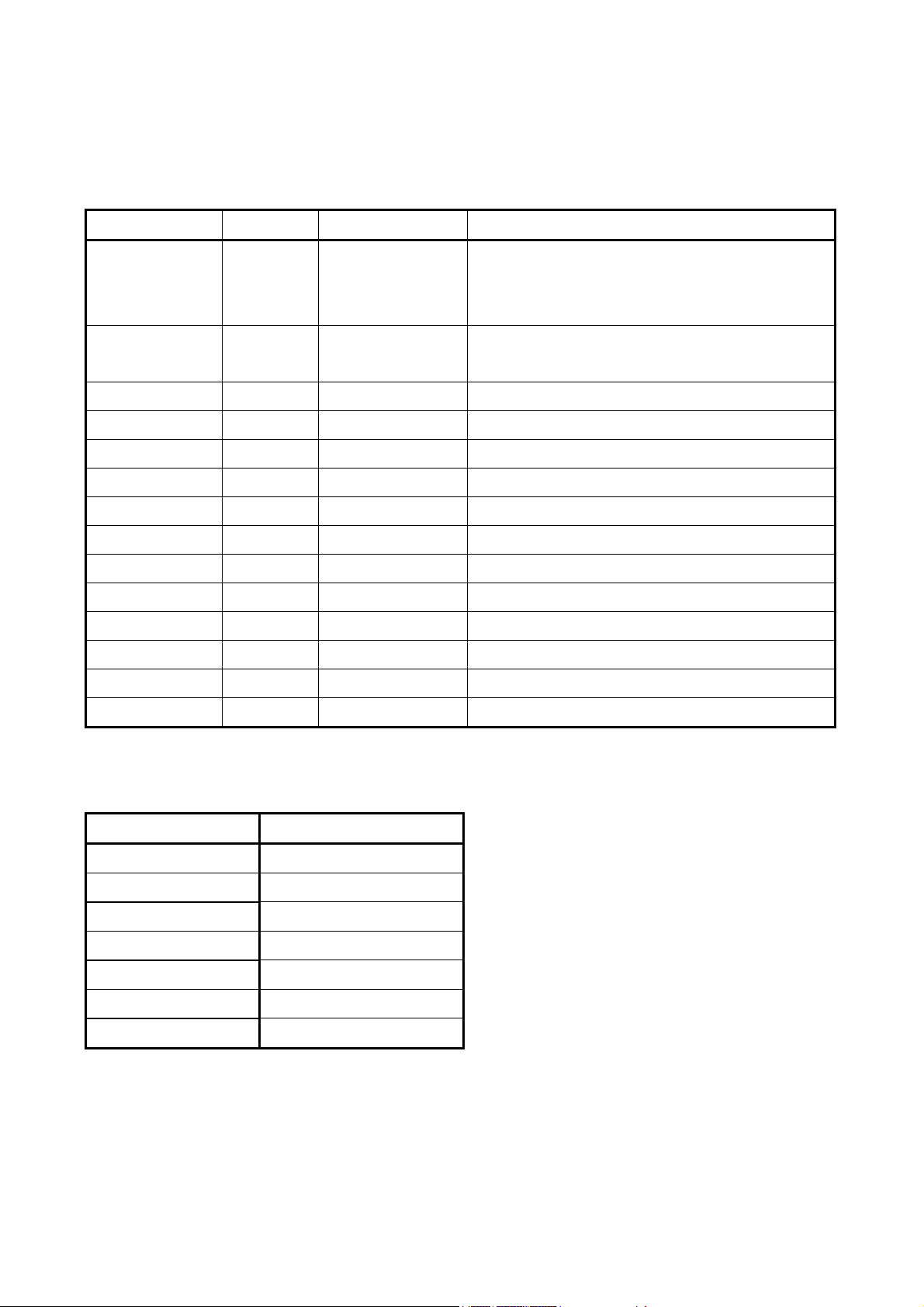
Power Supply Unit:
Power Supply Voltage Control Signal Use
VP BATTERY N/A PRIMARY POWER SUPPLY
VOLTAGE PANASONIC LR6*2
AC E-8AC (3.4V 2.5A)
+3.3VD +3.3V SDOK COACH 6 DSP I/O, SDRAM, NAND FLASH
, XD, FLASH BLOCK, CCD BLOCK
+3VAL +3V LCD_PW_EN LCD DRIVE
+3VTG +3V CCD_PW CCD, TG, VD, CDS
+3VCDS +3V CCD_PW CDS
+3.3VM +3.3V SPM MOTOR DRIVE
+3.3VZ +3.3V ZOOM_PI_EN LENS ZOOM FUNCTION
+3.3VF +3.3V FOCUS_PI_EN LENS FOCUS FUNCTION
+1.8VD +1.8V SPM COACH 6 CORE
+12VCCD +12V CCD_PW CCD VH
-8VCCD -8V CCD_PW CCD VL
+8.5VD +8.5V BACKLIGHT LCD BACKLIGHT
+8.5VL +8.5V LCD_PW_EN LCD PANEL
+5VD +5V LCD_PW_EN LCD DRIVE, IGBT
Control Signal Polarity:
Control Signal Power Status
SPM HIGH POWER ON
SDOK LOW POWER ON
LCD_PW_EN HIGH POWER ON
CCD_PW HIGH POWER ON
ZOOM_PI_EN HIGH POWER ON
FOCUS_PI_EN HIGH POWER ON
BACKLIGHT HIGH POWER ON
H-3
Page 4
H. DESCRIPTION OF MECHANISM X-450/C-370/D-535
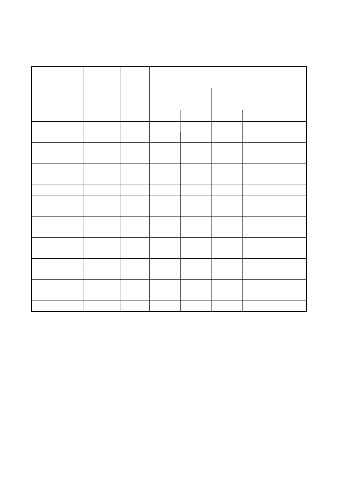
Power Supply Status For Primary Action Mode:
Control Signal Power
Supply
Camera
Off
Camera On
Preview Playback USB
Mode Mode
TFT On Video TFT On Video
Mode
VP ON ON ON ON ON ON
SPM +3.3V OFF ON ON ON ON ON
+3.3VM OFF ON ON ON ON ON
+1.8VD OFF ON ON ON ON ON
+15VD OFF ON ON ON ON ON
-10VD OFF ON ON ON ON ON
+8.5VD OFF ON ON ON ON ON
SDOK +3.3VD OFF ON ON ON ON ON
CCD_PW +3VTG OFF ON ON OFF OFF OFF
+3VCDS OFF ON ON OFF OFF OFF
+12VCCD OFF ON ON OFF OFF OFF
-8VCCD OFF ON ON OFF OFF OFF
LCD_PW_EN +3VAL OFF ON OFF ON OFF OFF
+8.5VL OFF ON OFF ON OFF OFF
+5VD OFF ON OFF ON OFF OFF
ZOOM_PI_EN +3.3VZ OFF ON ON OFF OFF OFF
FOCUS_PI_EN +3.3VF OFF ON ON OFF OFF OFF
BACKLIGHT +8.5VD OFF ON OFF ON OFF OFF
[2] Description of Each Substrate
1. Flash Board
IC U400 AT1452 Charge:
After switching on the flash mode, DSP will detect if the voltage “Strobe_V” is the standard
default value. If it is not, charge is HI level and start to charge. When charge achieves the
standard default value, the charge is LOW level and stop charging. Strobe_V will increase
with the increasing charge voltage during the charge process. Charge will stop till achieving
the F/W setting value. At this time, Strobe signal is available to activate. When Strobe
signal turn into HI level from LOW level, Q401 is conducting and flash is triggering. Please
refer to the figures 4.1.1 and 4.1.2 for above mention.
H-4
Page 5

H. DESCRIPTION OF MECHANISM X-450/C-370/D-535
Fig. 4.1.1 Charge Waveform
Fig. 4.1.2 Discharge Waveform
H-5
Page 6

H. DESCRIPTION OF MECHANISM X-450/C-370/D-535
Pin No. Symbol I/O Description
1 CHARGE I Charge enable input
2 FB I Error amplifier input
3 DUTY I Duty control input
4 GND - Ground
5 OUT O Push-pull output
6 VCC - Power supply
7 READY O Charge ready open drain output
8 SS I Soft-start setting
Caution:
The voltage for the big capacitor and flash tube is 300V. Please remove the power resource
and discharge the capacitor before repair. Flash tube polarity is as below:
H-6
Page 7
H. DESCRIPTION OF MECHANISM X-450/C-370/D-535
2. Power Block
Power Manager IC Control Signal Use
U6: MAX1567ETL SPM CH1~CH6 ON/OFF
PWM method for step up & down 6CH DC/DC POWER IC.
·
The arrangements for each channel are as below:
Channel Use
CH1 +3.3V
CH2 +3.3VM
CH3 +1.8VD
CH4 +15VD
CH5 -10VD
CH6 +8.5VD
Oscillation frequency is 600kHz.
·
U6 PIN22 connects to C77 and R107. They will decide the frequency of triangle waveform.
· Protection circuit for short circuit
For CH1, CH3 & CH5, There is protection for pass current in U6.
For CH2, CH4 & CH6, There is protection for pass current in F1 fuse.
· D12, U8 & Q41
D12, U8 & Q41 will form OVP. J4 DC JACK INPUT MAX. 6.3V.
· LCD back light constant current circuit
R409, R411, R412, Q402 & Q403 form the constant current circuit.
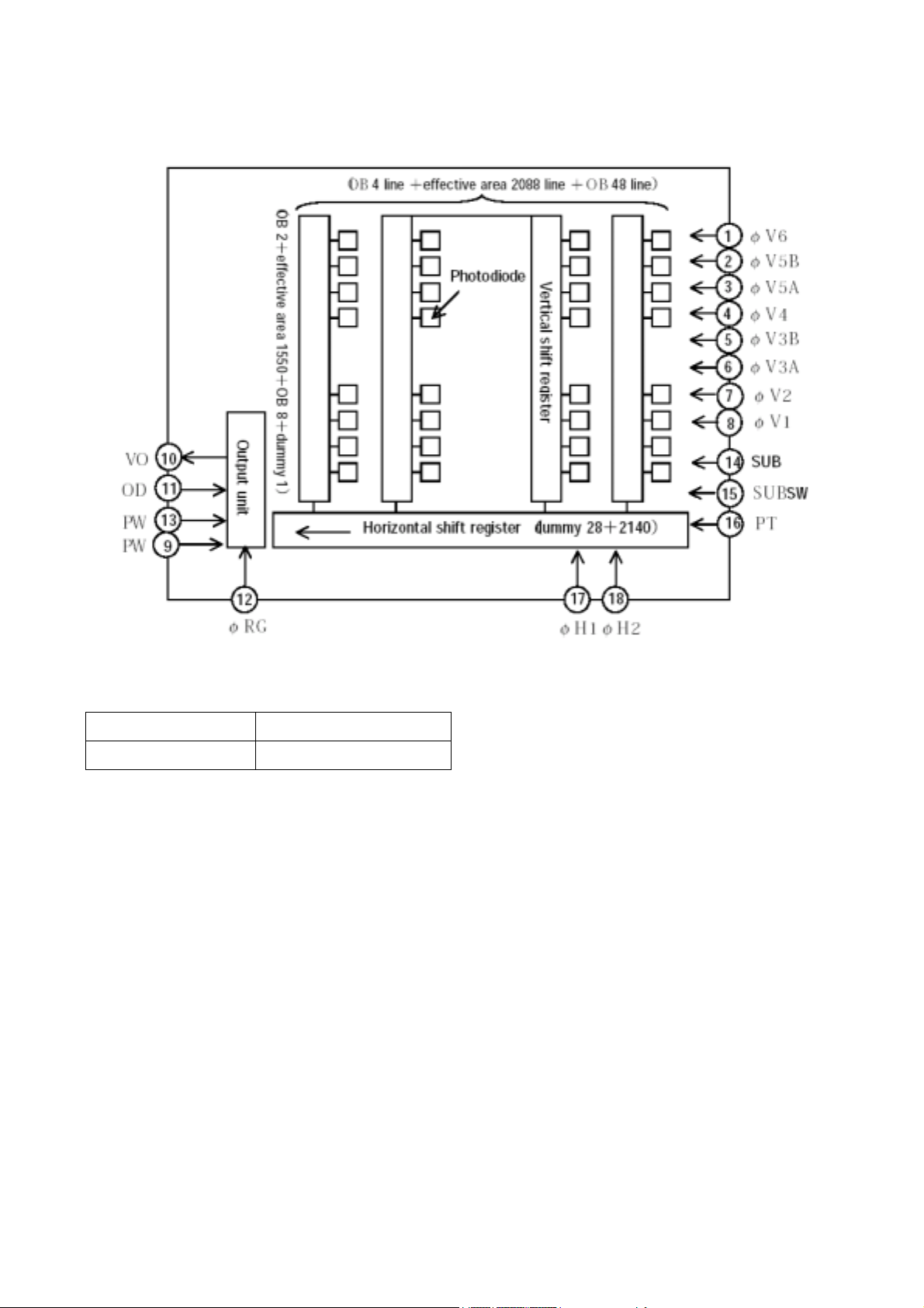
3. CCD Board
· U1 (CCD), U3 (CDS/ADC), U5 (VD), U6 (TG) form the CCD circuit
· U2, U4, U7 (REGULATOR) form the CCD power supply circuit
H-7
Page 8
H. DESCRIPTION OF MECHANISM X-450/C-370/D-535
U6 (TG)
·
Y1 Crystal oscillator
Crystal Pixel Clock
49.0909MHz 24.54545MHz
Y1 oscillates as 49.0909MHz square wave to TG then generate Pixel Clock. After Inputting
Pixel Clock to ZORAN DSP, it will generate the Level Synchronous Signal & Vertical
Synchronous Signal to U6 (TG). According to this output signal & firmware TG work mode
setting, it will generate the signal to drive CCD.
U5 (VD)
·
U6 (TG) sends out the Vertical Synchronous Signal for transmitting CLOCK and Shutter
(SUB) Pulse to U5 (VD). After receiving the signal, the amplitude of U5 will increase then
drive the CCD.
· U3 (CDS/ADC)
The output signal CCD_OUT which is for CCD (U1) will pass through Q1 (BUFFER) then
reach to U3 (CDS).
H-8
Page 9

H. DESCRIPTION OF MECHANISM X-450/C-370/D-535
U3 is formed with CDS (Correlated Double Sampling), VGA (Variable Gain Amplifier) and
ADC (A/D Convector).
CDS will remove the partial signal which is overlap the CCD OUT then get the correct signal
for pixel.
VGA will change the amplitude of CCD_OUT which is processed after CDS by ISO setting.
ADC will transform the CCD_OUT signal which is proceed after VGA into 10 bit digital
signal. Then transmit to ZORAN DSP to form the digital image.
CCD CLK Synchronous Signal instruction
·
CCD CLK Synchronous Signal
Name Amplitude Frequency
CCLK Pixel Clock 3V f = 24.545454MHz
HD Level Synchronous Signal 3V f = 7.867KHz
VD Vertical Synchronous Signal 3V f = 30Hz
H-9
Page 10

H. DESCRIPTION OF MECHANISM X-450/C-370/D-535
CCD CLK Drive Signal
Name Amplitude Frequency Note
H1 Level Signal 3V(Low=0V, High=3V) f = 24.545454MHz HD Synchronous Signal
H2 Level Signal 3V(Low=0V, High=3V) f = 24.545454MHz HD Synchronous Signal
V1 Vertical Signal
f = 7.867KHz
High=+12V)
V2 Vertical Signal 20V(Low=-8V, Mid=0V) f = 8.58KHz
20V(Low=-8V, Mid=0V,
20V(Low=-8V, Mid=0V,
V3 Vertical Signal
f = 8.58KHz
High=+12V)
V4 Vertical Signal 20V(Low=-8V, Mid=0V) f = 8.58KHz
20V(Low=-8V, Mid=0V,
V5 Vertical Signal
f = 8.58KHz
High=+12V)
V6 Vertical Signal 20V(Low=-8V, Mid=0V) f = 8.58KHz
20V(Low=-8V, Mid=0V,
V7 Vertical Signal
f = 8.58KHz
High=+12V)
20V(Low=-8V, Mid=0V,
V8 Vertical Signal
f = 8.58KHz
High=+12V)
3 LEVEL TRANS
PULSE OUTPUT
2 LEVEL TRANS
PULSE OUTPUT
3 LEVEL TRANS
PULSE OUTPUT
2 LEVEL TRANS
PULSE OUTPUT
3 LEVEL TRANS
PULSE OUTPUT
2 LEVEL TRANS
PULSE OUTPUT
3 LEVEL TRANS
PULSE OUTPUT
3 LEVEL TRANS
PULSE OUTPUT
RG 3.0 Vpp f = 24.545454MHz Continuous Waveform
VSUB 20 Vpp f = 7.867KHz Setting Period Output
· CCD Board Power On Sequence
H-10
Page 11

CCD Waveform
·
H. DESCRIPTION OF MECHANISM X-450/C-370/D-535
4. MCU Block
· ALL
ZORAN DSP BLOCK
SDRAM BLOCK
USB BLOCK
FLASH MEMORY BLOCK
XD BLOCK
LES I/F BLOCK
TFT I/F BLOCK
VIDEO BLOCK
· ZORAN DSP BLOCK
U2 ZORAN DSP CIRCUIT includes RTC, image process, image compression, image
display, memory I/F, external I/F, flash control and lens control.
MAIN CRYSTAL-Y2 13.5MHz oscillator for U2 ZORAN DSP. System Main Clock.
RTC (Real Time Clock)- Y1 32.768MHz oscillator for U2 ZORAN DSP. Time setting &
management.
H-11
Page 12

H. DESCRIPTION OF MECHANISM X-450/C-370/D-535
IMAGE PROCESS-AE, AWB & AF control.
IMAGE COMPRESSION-JPEG & Motion JPEG.
IMAGE DISPLAY-TFT, Video NTSC/PAL output signal process.
MEMORY I/F-SDRAM, Flash Memory & xD I/F.
EXTERNAL I/F-Key Switch I/F, LED control & Mode Dial I/F.
FLASH CONTROL- Flash Charge & Lightening control.
LENS CONTROL-Lens motion control.
SDRAM BLOCK
·
U7 (SDRAM) Composition Circuit.
U7 (SDRAM) is 128MB(2M/16bit/4bank)SDRAM.
The transmission speed between U7 (SDRAM) & U2 (ZORAN DSP) is 108MHz.
· USB BLOCK
J5 (USB JACK)
USB (Universal Serial Bus) specification is 1.1, full speed 12MBPS.
· FLASH MEMORY BLOCK
U5 (FLASH MEMORY) Composition Circuit.
U5 (FLASH MEMORY) is used for saving DSP CORE, camera setting, operating,
adjustment value & picture.
· xD BLOCK
JC2(xD CARD CONNECTOR) Composition Circuit
xD power supply is +3.3VD
LENS I/F BLOCK
·
J3 (LENS I/F DRIVE) Composition Circuit
J3 (LENS I/F DRIVE) is for controlling FOCUS, ZOOM, SHUTTER, IRIS MOTOR, FOCUS
PI (Photo Interrupt) & ZOOM LENS PR (Photo Reflect).
·
TFT I/F BLOCK
U401 (LCD DRIVE) & J401 (LCD CONNECTOR) Composition Circuit
· VIDEO BLOCK
JC1 (TV JACK) Composition Circuit
H-12
Page 13

H. DESCRIPTION OF MECHANISM X-450/C-370/D-535
Video Image Signal Waveform
H-13
 Loading...