NSC CLC520MDC, CLC520AJP, CLC520AJE-TR13, CLC520AJE, CLC520AD-MLS Datasheet
...
Features
■
160MHz, -3dB bandwidth
■
2000V/µsec slew rate
■
0.04% signal nonlinearity at 4Vppoutput
■
-43dB feedthrough at 30MHz
■
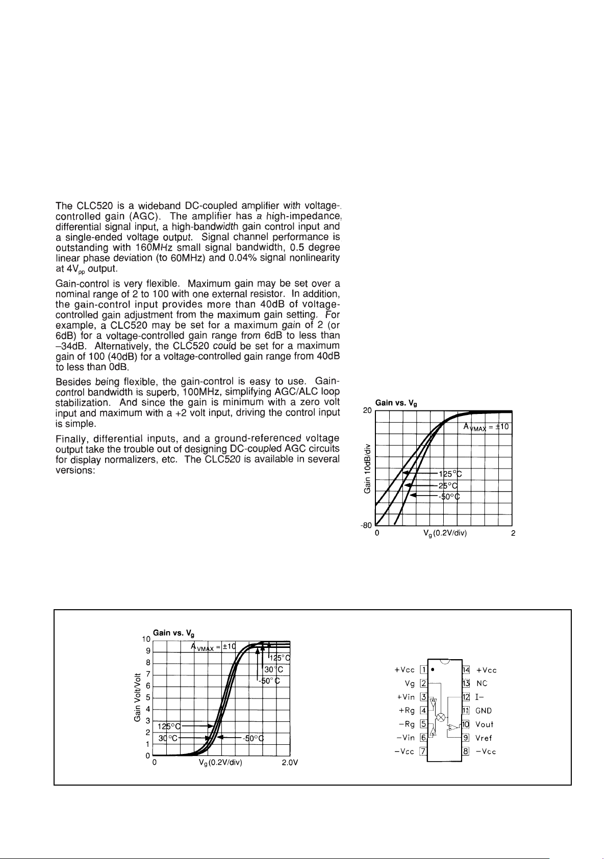
User adjustable gain range
■
Differential voltage input and
single-ended voltage output
Applications
■
Wide-bandwidth AGC systems
■
Automatic signal-leveling
■
Video signal processing
■
Voltage controlled filters
■
Differential amplifier
■
Amplitude modulation
General Description
CLC520
Amplifier with Voltage Controlled Gain, AGC+Amp
N
June 1999
CLC520
Amplifier with Voltage Controlled Gain, AGC+Amp
Pinout
DIP & SOIC
© 1999 National Semiconductor Corporation http://www.national.com
Printed in the U.S.A.
CLC520AJP -40°C to +85°C 14-pin plastic DIP
CLC520AJE -40°C to +85°C 14-pin plastic SOIC
CLC520ALC -40°C to +85°C dice
CLC520AMC -55°C to +125°C dice qualified to Method 5008,
MIL-STD-883, Level B
DESC SMD number: 5962-91694

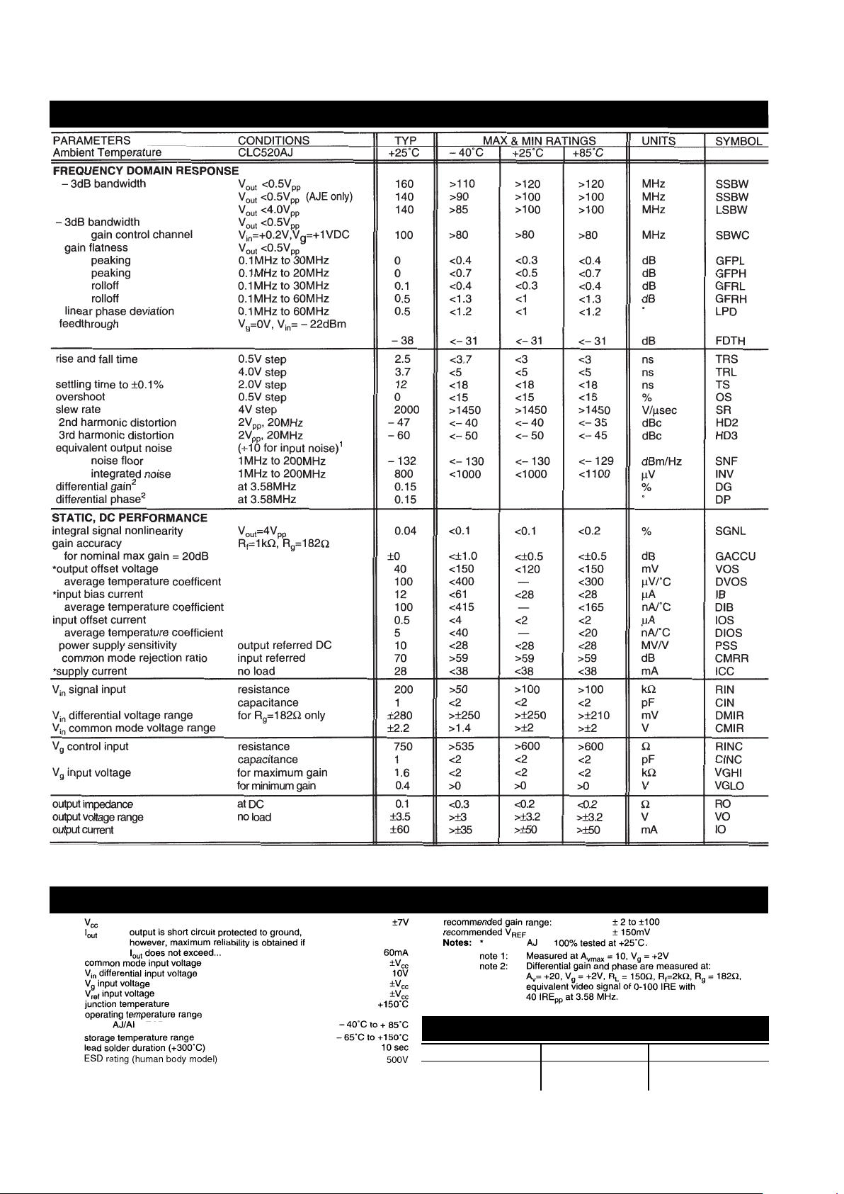
CLC520 Electrical Characteristics
(Av= +10,Vcc= ±5V,RL= 100Ω,Rf= 1kΩ,Rg= 182Ω, Vg= +2V)
Absolute Maximum Ratings Miscellaneous Ratings
Min/max ratings are based on product characterization and simulation. Individual parameters are tested as noted. Outgoing quality levels are
determined from tested parameters.
2 http://www.national.com
Pac kage Thermal Resistance
Package
θθ
JC
θθ
JA
AJP 55°C/W 105°C/W
AJE 45°C/W 120°C/W
Transistor Count 42

Typical Performance Characteristics
(TA= 25°, Av= +10,VCC= ±5V, RL= 100
ΩΩ,,
Rf= 1kΩΩ,Rg= 182ΩΩ,Vg= +2V )
3 http://www.national.com
 Loading...