

Page 1

nokia
Product NHM-5 Repairhints
Service & Competence Center Europe Introduction Version 1.0 Approved
Customer Care Training Group Date 2001-03-27
CONFIDENTIAL
1 (29)
Repairhints
3310
NHM-5
HDa 12
© NMP 2001
Checked by:
CC Training Group
Approved by:
SCCE
Page 2
nokia
Product NHM-5 Repairhints
Service & Competence Center Europe Introduction Version 1.0 Approved
Customer Care Training Group Date 2001-03-27
CONFIDENTIAL
2 (29)
GENERAL
-How to use this document
Put the QUICK REPAIR layouts behind this manual.
Now you are able to follow these specifications with graphical layouts and it is easier for you to find the
components and measuring points.
-Component characteristics:
Some components contain important data.
Several described steps are only practicable if you are able to reflash/ realign the phone and/or rewrite
IMEI/SIMlock in certain cases. Please pay attention to separate notes.
-Underfills, broken balls, µBGA
It is not possible to change underfilled components. The trial will damage PCB surely. All replaceable
µBGA-components must be renewed after removing. Reflow is not allowed.
Check soldering points, remove oxidated solderings (broken balls) carefully by enclosing few new solder
before placing new components.
µBGA must be soldered only with NMP approved µBGA-rework machines (e.g. Zevac/OK International).
Use only recommended Fluxtype and an appropriate amount of it.
-PCB handling & cleaning
Only use appropriate cleaning materials, don`t use scratching or rubbing tools. Clean PCB carefully after
every rework and take great pains over the keyboard area. Don´t make any loose wiring connections
anywhere.
If it is necessary to clean the PCB, please pay attention to the following: Because of organic surface
protection (OSP), cleaning must only be done with a lint-free cloth which may be moisten with DI-water.
IPA or other solvent like ethanol should only be used to clean gold pads for spring contacts without
affecting the surrounding copper layers.
If it is necessary to change any item located under the metal shields, remove the shield first, don´t cut
partially or bend it.
-Realign after repair
Characteristics of replacement parts are different.
To prevent additional faults after repair (eg. low standby time, loosing network etc.) it is necessary
to retune phone values after repair.
© NMP 2001
Checked by:
CC Training Group
Approved by:
SCCE
Page 3

nokia
CONFIDENTIAL
3 (29)
Product NHM-5 Repairhints
Service & Competence Center Europe Introduction Version 1.0 Approved
Customer Care Training Group Date 2001-03-27
IMPORTANT:
This document is intended for use by authorized NOKIA service centers only.
The purpose of this document is to provide some further service information for NOKIA 3310 phones.
It contains a lot of collected tips and hints to find failures and repair solutions easily.
It also will give support to the inexperienced technicians.
Saving process time and improving the repair quality is the aim of using this document.
We have build it up based on fault symptoms (listed in "Contents") followed by detailed description for further
analysis.
It is to be used additionally to the service manual and other service information like Service Bulletins, for that
reason it doesn't contain any circuit descriptions or schematics.
All measurements are made using following equipment:
Nokia repair SW : WinTesla Version 6.43
DLL version : 311.03.00
Nokia Module Jig : MJS-19
Digital multimeter : Fluke 73
Oscilloscope : Hitachi V-1565; Fluke PM 3380A/B
Spectrum Analyzer : Advantest R3131 with an analogue probe
RF-Generator / : Rohde & Schwarz CMU 200
GSM Tester
While every endeavour has been made to ensure the accuracy of this document, some errors may exist. If any errors
are found by the reader, NOKIA should be notified in writing, using following procedure :
Please state:
Title of the Document + Issue Number/Date of publication.
Page(s) and/or Figure(s) in error.
Please send to: Nokia GmbH
Service & Competence Center Europe
Meesmannstr.103
D-44807 Bochum / Germany
Email: training.sace@nokia.com
© NMP 2001
Checked by:
CC Training Group
Approved by:
SCCE
Page 4
nokia
CONFIDENTIAL
4 (29)
Product NHM-5 Repairhints
Service & Competence Center Europe Introduction Version 1.0 Approved
Customer Care Training Group Date 2001-03-27
Contents
GENERAL 2
INTRODUCTION 3
HARDWARE CHANGES 5
PHONE DOESN´T SWITCH ON 6
FLASH UPDATE NOT POSSIBLE 8
PHONE SWITCHES OFF 9
LOW STANDBY TIME 10
NOT CHARGING 12
CONTACT SERVICE 14
SIMCARD FAULTS 15
AUDIO FAULTS 18
USER INTERFACE FAULTS 19
NO SERVICE 21
FREQUENCY LIST 29
© NMP 2001
Checked by:
CC Training Group
Approved by:
SCCE
Page 5
nokia
CONFIDENTIAL
5 (29)
Product NHM-5 Repairhints
Service & Competence Center Europe Introduction Version 1.0 Approved
Customer Care Training Group Date 2001-03-27
HW-CHANGES IN 3310/NHM-5/HDa 12
Intermittent switches off problem ( SB 12 )
In case of HW-ID 0600, 0601,0602, 0603, 0604, 0607, 0608, 0612 and 0614 change following parts:
R559 from 2.2kΩ to 1kΩ (1430754)
C559 from 100pF to 47pF (2320552)
C560 from 1nF to 47pF (2320552)
C303 from 1nF to 47pF (2320552)
Since HW-ID 0615 these changes are implemented in production.
Software update to PhoneSW 4.06 or higher makes above mentioned HW update unnecessary (SB16)
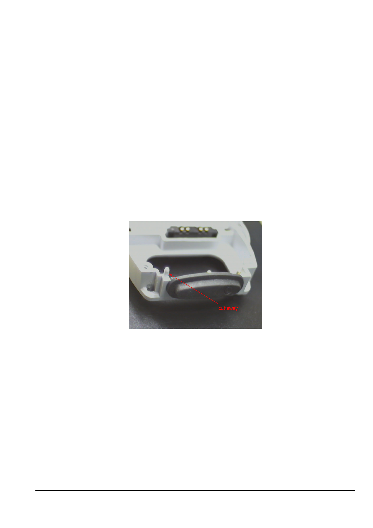
Difficulties when removing B-Cover ( SB 13 )
If customers critisize bad removal of B-Cover cut away the guiding pin of the D-Cover ( see picture below )
After this procedure it is necessary to assemble the phone with a torque screwdriver prepared for 30Ncm!
© NMP 2001
Checked by:
CC Training Group
Approved by:
SCCE
Page 6
nokia
CONFIDENTIAL
6 (29)
Product NHM-5 Repairhints
Service & Competence Center Europe Introduction Version 1.0 Approved
Customer Care Training Group Date 2001-03-27
PHONE DOESN`T SWITCH ON
Phone doesn`t
switch on
Check current consumption
Off state: 0.1-0.6 mA
Sleepmode: 0.6-4 mA
Call mode: 100-550 mA,
if too high, continue with
section "LOW
STANDBY/OPERATION MODE
TIME"
Disable watchdog if phone
switches off after 2-3
seconds
nOK
Check Vb 3.6V at
C227/228
OK
Check
32.768kHz at C220,
3Vpp squarewave
Check X203 if bent
or soiled, check
L513,L201
nOK nOK
Check/change
B200,R211/212/214,
C229/230
Change N201
OK
Check if
PWRONX at R402 drops
to 0V during
powerswitch-use
OK
Check
Vbb 2.8V at
C209/211
OK
Check Vxo 2.8VDC at
C243
OK
Check
Vcore 1.7VDC at both
pads of L200, change if
necessary.
OK
Check SLEEPX
2.8VDC at J308
OK
Check
PURX 2.8V DC at
R308 after
Powerkey-press
nOK
Check/change
S419,R402,R224,
Change N201 if necessary
nOK
Check resistance of line
to GND (~90k). If line OK,
change N201
nOK
Check resistance of line
to GND (~45k). If line OK,
change N201
nOK
Check resistance of line
to GND (~180k). If line
OK, change N201
nOK
OK OK OK
MAD is faulty in all
probability. Swap phone,
MAD is not changeable
Check 13MHz
REFCLK at C303
(500mVpp)
Try to flash the
phone
Phone is OK
nOK nOK
Change N201
Check values around
G502,N500,V502
nOK
Continue with section
"FLASH UPDATE NOT
POSSIBLE"
© NMP 2001
Checked by:
CC Training Group
Approved by:
SCCE
Page 7

nokia
CONFIDENTIAL
7 (29)
Product NHM-5 Repairhints
Service & Competence Center Europe Introduction Version 1.0 Approved
Customer Care Training Group Date 2001-03-27
X203 Battery connector
Check if bent or soiled.
Check that pads of connector on PCB are clean.
S419 Power on/off switch faulty
Check that voltage at R402 is 3.6V when powerswitch is not pressed.
If voltage is not ok, check R402 and R224, change N201 if necessary.
If voltage at R402 is ok, it must decrease to 0V if S419 is pressed, else change S419.
Disable watchdog by connecting R224 to GND if phone switches off after 2 or 3 seconds.
B200 Sleep Clock Oscillator faulty
Check 32.768kHz, 3Vpp squarewave at pad of C220 located towards B200.
If oscillator does not work, check voltage at the two pads of B200 which are located
towards N201, normally 1.6V DC. If not ok, check periphery of B200 or change CCONT N201.
If frequency is not ok, check parts around B200 (R211, R212, R214, C229/230).
G502 Reference oscillator faulty
Check Vcc 2.7V DC at G502 pin 2 and Vcont (varies between 0.03V and 2.3V, typically 1.3VDC) at C552.
Check 26MHz Clk-frequency at pin 3 of G502, 1Vpp
Check 13MHz Clk-frequency at C559, 300mVpp
If not ok, check voltages for HAGAR N500. (Detailed information in chapter “No Service”).
Check 13MHz Clk-frequency at C303, 500mVpp at pad located towards V103.
If not ok, check values around V502
N201 CCONT faulty
Check Vb 3.6V DC at C227/228.
Check 32.768kHz, 3Vpp squarewave at pad of C220 located towards B200.
Check that PWRONX decreases from 3.6V DC to 0V at R402 if powerswitch is
pressed.
If these conditions are fulfilled output voltage lines should rise to their intended values
and PURX is released after some milliseconds by CCONT.
If CCONT does not work, check output voltage lines for shorts to ground ( check current consumption! ),
if ok, change CCONT with µBGA soldering machine and run energy management calibration.
D300 MAD faulty
Check 32.768kHz squarewave at C220.
Check 13MHz Clk-frequency at C303.
Check Vbb 2.8V DC at C209/211 and Vcore 1.7V DC at L200.
Check SLEEPX 2.8V DC at J308.
Check PURX 2.8V DC at R308.
Try to flash the phone.
MAD is probably faulty, swap the phone because MAD is not changeable.
© NMP 2001
Checked by:
CC Training Group
Approved by:
SCCE
Page 8
nokia
CONFIDENTIAL
8 (29)
Product NHM-5 Repairhints
Service & Competence Center Europe Introduction Version 1.0 Approved
Customer Care Training Group Date 2001-03-27
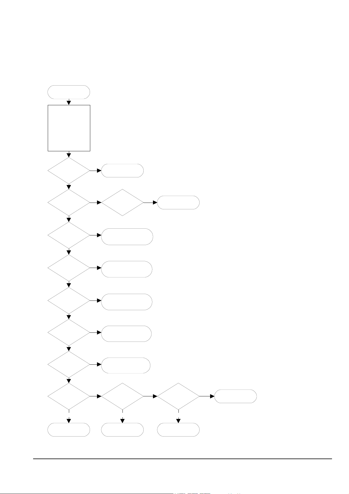
FLASH UPDATE NOT POSSIBLE
Flash update not
possible
Prommer fault code
1. MCU boot failure
2. Serial clock line failure
3. Serial data line failure
yes
Connect "watchdog disable"
R224 to GND if phone does
not stay on
OK
Check Vbb 2.8V at C209/211
Vxo 2.8V at C243
Vcore 1.7V at L200
nOK
no
Continue with section
"Phone doesn`t switch
on"
Algorithm code fail,
alias ID missing
yes
Update FP box with latest
flash device list, try to
update again
nOK
no
Change Flash D301, try
to update again. If not
ok, MAD or PCB faulty
External RAM failure
yes
Change SRAM D302, try to
update again
nOK
OK
Check SLEEPX 2.8V
at J308
OK
Check PURX 2.8V at R308
OK
Check 13MHz RFCLK at C303
500mVpp
OK
Check M/F-bus lines (X201,
pad 1,2,4) for shorts to GND,
also check R217,
R302/304/307, C232 and
V204
OK
nOK
nOK
nOK
MAD is faulty in all
probability, swap the
phone.
Change CCONT N201
Check values around
G502, N500, V502
If update is still not possible,
swap the phone, because MAD or
PCB should be the reason
© NMP 2001
Checked by:
CC Training Group
Approved by:
SCCE
Page 9

nokia
CONFIDENTIAL
9 (29)
Product NHM-5 Repairhints
Service & Competence Center Europe Introduction Version 1.0 Approved
Customer Care Training Group Date 2001-03-27
PHONE INTERMITTENT SWITCHES OFF/DOESN`T SWITCH ON
Check first of all phone´s software version.
If version is < 4.06, make SW update and check if fault persists.
If phone switches off intermittent although phone SW is 4.06 or higher and battery is fully charged,
check phone´s HW-ID.
In case of HW-ID 0600, 0601,0602, 0603, 0604, 0607, 0608, 0612 and 0614 it is necessary
to change the following parts:
R559 from 2.2kΩ to 1kΩ (1430754)
C559 from 100pF to 47pF (2320552)
C560 from 1nF to 47pF (2320552)
C303 from 1nF to 47pF (2320552)
If HW-ID is 0615 or higher, the above mentioned changes are already done.
Other possibilities if SW- and/or HW-update do not solve the problem:
Check mechanical appearance of connector X203.
Check that pads of X203 on PCB are clean.
Check amplitude of 32.768kHz at C220, 3Vpp squarewave,
probably broken solderings under CCONT N201. Remove CCONT and replace it with µBGA soldering machine,
run energy management calibration after changing CCONT.
The same problem may be caused by N500, because the reference oscillator G502 ( 26MHz ) is divided to
13MHz system clock by HAGAR N500.
© NMP 2001
Checked by:
CC Training Group
Approved by:
SCCE
Page 10

nokia
CONFIDENTIAL
10 (29)
Product NHM-5 Repairhints
Service & Competence Center Europe Introduction Version 1.0 Approved
Customer Care Training Group Date 2001-03-27
LOW STANDBY/OPERATION MODE TIME
Check power
consumption of
phone
OK
Off state 0.1-0.6mA
OK
nOK nOK
Lift L513
check current
OK
Resolder
L513, lift L201,
check current
OK
Check Capacitors in VB line
(C200/201,C226-228...), change
N200/201 or N400 if necessary
nOK
Check capacitors
C563/564 C570-572
or change N502
Check
C233/527/575/597
Sleep mode 0.6-4mA
Check charging
circuit, run energy
management
calibration
Calibrate RX/TX
Note that standby time also
depends on network side, like PRP,
signal strength, location updates
and user´s handling.
OK
OK
values
OK
Check resistance of
nOK nOK
output voltage lines
of CCONT to GND
OK
Change CCONT N201
nOK
nOK
Check components in
corresponding lines
Continue with
section "NOT
CHARGING"
Continue with
section "NO
SERVICE"
© NMP 2001
Checked by:
CC Training Group
Approved by:
SCCE
Page 11

nokia
CONFIDENTIAL
11 (29)
Product NHM-5 Repairhints
Service & Competence Center Europe Introduction Version 1.0 Approved
Customer Care Training Group Date 2001-03-27
Check current consumption in different operation modes:
Function mode Minimum current in mA Maximum current in mA
Off state 0.1 0.6
Sleep mode 0.6 4
Call mode GSM 900 130 550
Call mode GSM 1800 100 530
Off state current fail
Lift L513 to define the fault if off state current is not ok.
If current is still not ok, lift C563/564 and C570-572 one by one or change
power amplifier N502, which is the reason in most cases.
If current is ok after removing L513, resolder it and lift L201. If current is too high,
check capacitors C233,C527,C575 and C597. If current consumption is ok after lifting L201,
you have to check capacitors in Vb-line ( eg C200/201, C226-228,C247…) or change N200/201, N400.
Sleep mode current fail
Check resistance of output voltage lines of CCONT N201 to ground.
Resistance should be higher than 10kΩ except Vsyn1 ( ~ 4.7kΩ ),
if resistance of any line is not ok, check/change parts of this line,
if resistance of all lines is ok, change CCONT N201.
If the standby/operation mode time is still not ok, check charging circuit and
run the energy management calibration.
It also can be necessary to calibrate the Rx/TX values of the phone.
© NMP 2001
Checked by:
CC Training Group
Approved by:
SCCE
Page 12

nokia
CONFIDENTIAL
12 (29)
Product NHM-5 Repairhints
Service & Competence Center Europe Introduction Version 1.0 Approved
Customer Care Training Group Date 2001-03-27
NOT CHARGING
Nothing happens if
charger is connected
Check
Voltage Level at R210
>0.4V if charger is
connected
OK
Change N200, N201
"Not charging"
appears on LCD
nOK
Check/change
X200,F200,
V201,L202,C215-217
Run energy
management
calibration
OK
Try to charge after
calibration
FAILURE MESSAGES
Battery temperature failed Battery size failed Battery voltage failed Charge current failed Charge voltage failed
Check X203,
R220/222, change
N201
Check X203,
R221/222, change
N201
Change N201
Check R204, change
N200, N201
Check Vcharge at
voltage divider
R209/210
OK
Change N201
nOK
Check X200,F200,V201,
L202,C215-217, change
N200
© NMP 2001
Checked by:
CC Training Group
Approved by:
SCCE
Page 13

nokia
CONFIDENTIAL
13 (29)
Product NHM-5 Repairhints
Service & Competence Center Europe Introduction Version 1.0 Approved
Customer Care Training Group Date 2001-03-27
X200 DC/HS connector, X203 battery connector
Check mechanical appearance of connectors,
make sure that pads for connectors on PCB are clean.
F200 faulty
Check resistance of fuse F200 ( 0 Ω )
CHRGR+ line short circuited to ground
Check resistance of CHRGR+ line at F200 to GND ( ~ 50 kΩ ),
if resistance is not ok, remove L202 and check again.
If resistance is ok now, C215/216 or N200 should be the reason,
if resistance is still not ok, V201 faulty in all probability, also check C217.
CCONT N201 faulty
Change CCONT if any A/D value is out of limit but DC voltage is ok.
If DC voltages are not ok, check corresponding voltage dividers and
battery connector X203.
Run energy management calibration after changing CCONT!
Energy management calibration
Run calibration:
- If charging stops too early or battery gets hot.
- If message „ not charging“ appears on LCD.
- If any part in the charging circuit has been replaced.
© NMP 2001
Checked by:
CC Training Group
Approved by:
SCCE
Page 14

nokia
CONFIDENTIAL
14 (29)
Product NHM-5 Repairhints
Service & Competence Center Europe Introduction Version 1.0 Approved
Customer Care Training Group Date 2001-03-27
CONTACT SERVICE
This fault means that the phone software is able to run and thus the watchdog of CCONT N201
can be served. Selftest functions run when power is switched on and software is executed
from flash. If any selftest fails, a “Contact Service“ text is shown on LCD.
Most common faults:
MCU ROM Checksum failed
Try to flash the phone. If not ok after flashing, probably D301 faulty. Change D301 with
µBGA soldering machine and try to update once more.
Note that you have to write back phone data and retune phone values after changing D301!
CCONT Interface failed
Probably faulty CCONT N201 or broken solderings under it.
Replace CCONT with µBGA soldering machine, run energy management calibration.
If not ok after reworking the CCONT, MAD or PCB faulty in all probability.
COBBA parallel/serial failed
Check Vbb 2.8V at C119 and VCOBBA 2.8V at C116/117
Check COBBAClk at J317
Probably COBBA N100 faulty or broken solderings under it – change COBBA.
If fault remains MAD or PCB faulty.
DSP Alive Test failed
In most of all DSP alive selftest failures MAD is faulty, which is not changeable.
Eeprom sec/tune checksum failed
Use WinTesla to check if phonedata like IMEI, product-code or PSN are corrupted.
If phone data is ok, try to reset the phone. If phone data is not ok or fault remains
after reset, change D301, write back phone data and retune phone values after changing D301!
© NMP 2001
Checked by:
CC Training Group
Approved by:
SCCE
Page 15

nokia
CONFIDENTIAL
15 (29)
Product NHM-5 Repairhints
Service & Competence Center Europe Introduction Version 1.0 Approved
Customer Care Training Group Date 2001-03-27
SIMCARD FAULT
"SIMcard not accepted"
Use WinTesla to
open quick/RF info window, compare
shown SIMlockdata with entries of the
respective product-code in
SIMlock list
nOK
Rewrite SIMlockdata with Nokia security
password or send this phone to SACE. If
SIMlock is corrected or inactive, but fault
remains, change COBBA N100 and rewrite
SIMlock once more
OK
SIMlock is OK. If the Msin data field
is closed to a special IMSI number
range, only the operator is allowed to
open the SIMlock. Also see general
SB 65
"Insert SIMcard"
Check SIMreader
if bent or soiled, check
contactpads on PCB
OK
Check
signals at pads for SIMreader:
Pad 1 SIMclk, Pad 2 SIMreset,
Pad 3/5 VSIM, Pad 6 SIMdata
nOK
Check R213, check SIMlines for
shorts, change V203/N201 if
necessary
nOK
nOK
Change SIMreader,
clean PCB if necessary
Probably MAD or PCB
faulty
© NMP 2001
Checked by:
CC Training Group
Approved by:
SCCE
Page 16

nokia
CONFIDENTIAL
16 (29)
Product NHM-5 Repairhints
Service & Competence Center Europe Introduction Version 1.0 Approved
Customer Care Training Group Date 2001-03-27
VSIM after switching on the phone without SIMcard. CCONT pulses up VSIM for four times, the first
time the amplitude is 3 Volt, the next three times it is 5 Volt.
If the phone is switched on with SIMcard VSIM stays on the level with which the SIMcard will work,
expected that SIMcard is not dirty or damaged.
Note that SIMClock and SIMData are only present when SIMcard is active, for example when phone registers to network.
SIMReset is low-active, that means that the SIMcard will be reseted when SIMReset is 0 Volt.
This is the case after switching on the phone ( diagram above ). While VSIM is already high,
SIMReset keeps low for a few milliseconds – in this time the card will be reseted.
© NMP 2001
Checked by:
CC Training Group
Approved by:
SCCE
Page 17

nokia
CONFIDENTIAL
17 (29)
Product NHM-5 Repairhints
Service & Competence Center Europe Introduction Version 1.0 Approved
Customer Care Training Group Date 2001-03-27
SIMcard-Reader
Check if bent or soiled, change if necessary
make sure that SIMreader´s pads on PCB are clean
V 203 faulty
Check resistance of SIMlines to ground, values shouldn’t decrease 200kΩ.
Also check C221/222/224/225.
N201 CCONT faulty
Check if VSIM rises to 3/5Volt after switching on the phone. If VSIM is ok but phone
does not recognize SIMcard, check SIMlines for shorts to ground or disconnections,
also check mechanical appearance of SIMreader.
If VSIM does not rise to its intended value, change CCONT N201. If fault persists after changing CCONT, probably
MAD or PCB faulty.
N100 COBBA faulty
If “SIMcard not accepted“ appears on LCD, but SIMlock-settings are ok or no SIMlock is set,
it is necessary to change COBBA N100.
Note that you have to rewrite SIMlock-data and tune Rx/TX-values of the phone after changing the COBBA.
© NMP 2001
Checked by:
CC Training Group
Approved by:
SCCE
Page 18

nokia
CONFIDENTIAL
18 (29)
Product NHM-5 Repairhints
Service & Competence Center Europe Introduction Version 1.0 Approved
Customer Care Training Group Date 2001-03-27
AUDIO FAULTS
No audio from
microphone
Change
Bottom-connector,
check function
nOK
Check MicBias at
V413 pin5: 2.4V on
active mic
OK
Check connection
between C120 and
Mic-pads on PCB
nOK
nOK
Check parts around V101,
check MIC-lines for shorts to
ground, change N100
Check solderings and
resistance of L402
No audio from
speaker
Check resistance of
speaker (30R),
change if bent or
soiled
OK
Check connection between
speakerpads on PCB and
C124. Not OK-check
R119/120
OK
Check resistance of
speakerlines to GND,
both >0.5M
OK
Change COBBA N100
Speaker faulty
Check resistance of speaker ( 30 Ω )
Check mechanical appearance of speaker if audio signal is too quiet or distorted.
Speakerlines short circuited to GND or disconnected
Check resistance of R119/120 ( 22 Ω ).
Check resistance of lines to GND ( > 0.5MΩ ).
Microphone doesn’t work
Check/change microphone,
make sure that pads for microphone on PCB are clean.
Check microphone voltage at V413 pin 5, 2.4 V on active micro.
Check connection between Mic-pads on PCB and R120, change COBBA N100 if necessary.
OK
Change COBBA
N100
© NMP 2001
Checked by:
CC Training Group
Approved by:
SCCE
Page 19

nokia
CONFIDENTIAL
19 (29)
Product NHM-5 Repairhints
Service & Competence Center Europe Introduction Version 1.0 Approved
Customer Care Training Group Date 2001-03-27
USER INTERFACE FAULTY
Display failure
Check mechanical appearance of display assy, change if necessary.
If LCD does not work after changing display assy check Vbb 2.8V DC at C409/413.
Voltage at C410/412 is normally 8V DC, check capacitors for shorts if voltage is not ok.
Check that voltage at J314 is 2.8V DC ( LCDReset ) – if line is short circuited to ground LCD does
not work. Also check that voltage at both sides of R306 is 2.8V DC.
If above mentioned values are ok but LCD does not work, probably MAD or PCB faulty
Keypad malfunktion
Check that contacts for keys on display assy are clean, make sure that PCB is not dirty
Check resistance of ROW and COL lines between the keys,
probably MAD faulty
Backlight failure
Check Vb 3.6V DC at anode of keypad/display-LED´s .
Check Vbb 2.8V DC pin 2 and Vb 3.6V DC pin 1 of N400.
Check resistance of R403 and R404.
Check signal KBlights 2.8V DC at pin 7/15 of N400. If voltage is ok but illumination does not work
change N400. If no voltage is measurable there may be a disconnection between D300 and
N400 or MAD is faulty.
If backlight switches itself on after assembling battery to the phone even though the phone keeps switched off, check R406/407
for shorts to ground. This fault occurs often in connection with liquid damages.
Vibra failure
Check contact springs of vibramotor, make sure that pads for vibramotor on PCB are clean.
Check Vb 3.6V DC at vibrapad located to the edge of the PCB, at the other pad and pin 16 of
N400, you can check vibrasignal with a scope ( waveform depends of chosen ringing-tone! ).
Check also R401.
Check Vb 3.6V DC at pin 1 and Vbb 2.8V DC at pin 2 of N400.
Check vibra_cnt at pin 19 of N400. If signal is ok but vibra does not work, change N400, else
there is a disconnection between D300 and N400 or MAD is faulty.
© NMP 2001
Checked by:
CC Training Group
Approved by:
SCCE
Page 20

nokia
CONFIDENTIAL
20 (29)
Product NHM-5 Repairhints
Service & Competence Center Europe Introduction Version 1.0 Approved
Customer Care Training Group Date 2001-03-27
Buzzer failure
Check mechanical condition / contact springs of buzzer
Check Vb 3.6V DC at E401
Check PWM- signal at E400 and pin 6 of N400.
Check Vb 3.6V DC at pin 1 and Vbb 2.8V DC at pin 2 of N400.
Check buzzer_cnt signal at pin 3 of N400. If signal is ok but buzzer does not work, change N400,
if signal is not ok, there may be a disconnection between D300 and N400, or Mad is faulty
Clock time problems
Clock time has to be corrected in short periods:
In case of this fault check amplitude and frequency of sleepclock-oscillator at C220,
should be 3Vpp squarewave at 32.768kHz.
If amplitude or frequency is not ok, change crystal B200. If fault persists, check parts around B200
like R211/212/214 and C229/230.
32.768kHz measured at pad of C220 located towards crystal B200.
© NMP 2001
Checked by:
CC Training Group
Approved by:
SCCE
Page 21

nokia
CONFIDENTIAL
21 (29)
Product NHM-5 Repairhints
Service & Competence Center Europe Introduction Version 1.0 Approved
Customer Care Training Group Date 2001-03-27
NO SERVICE / No or too low TX power GSM 900
First of all: Try to calibrate RX/TX values of the phone to define the fault
Use Wintesla to set phone in following mode: Initialise/ Local mode// Testing/ RF Controls/ active unit TX, Ch.38
Check 26MHz reference oscillator at G502 pin 3, 1Vpp, frequency deviation < +/-100Hz
Check TXI/Q signals at R541/548, refer to signals shown on next pages.
If not ok, check values at COBBA N100 (see below).
Check 897.6 MHz at L514. If not ok, check signals at HAGAR N500 (see below)
Check 897.6 MHz at C605. If not ok, check parts like T504, Z503 or V601.
Check 897.6 MHz at N502 pin 6. If not ok, check/change C600, R550 or N502.
Check 897.6 MHz at J502 ( Antenna pad ). If not ok, check L515 in & out, also check signal at
Z502 in & out and TXVGSM, 2.8Vpp squarewave at L509 ( sets Z502 to GSM TX-mode).
COBBA N100 faulty
Check Vbb 2.8V DC at C119 and VCOBBA 2.8V DC at C116/117.
Check 13MHz COBBAClock at J317 (see diagram in chapter “Contact Service“)
probably faulty COBBA N100 or broken solderings under it. Remove COBBA, replace it with
µBGA soldering machine, retune RX/TX values of the phone and rewrite SIMlock data.
HAGAR N500 faulty
Check voltages at HAGAR : VCTCXO 2.8V at C518
Vchp 4.8V at C505
Vsynte 2.8V at C501/504
Vrxrf 2.8V at C500
Vref_2 1.35V at C536
RXREF 1.2V at R507
Check 26MHz reference oscillator at G502 pin 3, 1Vpp, frequency deviation < 100Hz
Check TXI/Q signals at R541 and R548
Check Sdata at R300, Sclk/Sena at R301, check HAGAR Reset at C540, also check
TXC at C542 and TXP at J503 (diagrams on next pages).
Check frequency of SHF oscillator – TX Ch.38: 3590.4MHz.
If all values are ok but no TX signal is measurable at T504, probably faulty HAGAR or broken
solderings under it.
Remove HAGAR, replace it with µBGA rework machine and align RX/TX values of the phone.
G502 26MHz reference oscillator faulty
Check Vcc 2.7V at G502 pin 2 and Vcont (varies between 0.03V and 2.3V, typically 1.3VDC) at C552
If frequency deviation is higher than ± 100 Hz, it is necessary to change the oscillator.
G500 SHF oscillator faulty
Check (if possible) the frequency of G500 at T502 pin 3/4 – refer to frequencies worksheet
If you have no possibility to check frequency, you can check if oscillator works by
measuring Vcos 2.7V DC at C522 and voltage which adjusts G500 at C558, which varies
between 1.2V DC and 3.2V DC.
If voltage at C558 is 4.8V the oscillator doesn’t work in all probability or control loop is open.
Another possibility to check G500:
Activate phone to RX burst mode Ch38, do NOT connect RF generator to the phone. Now check 942.6MHz
(SHF-frequency divided by 4) at both sides of L504, amplitude is approximately –90dBm.
© NMP 2001
Checked by:
CC Training Group
Approved by:
SCCE
Page 22

Sena measured at R301
nokia
CONFIDENTIAL
22 (29)
Product NHM-5 Repairhints
Service & Competence Center Europe Introduction Version 1.0 Approved
Customer Care Training Group Date 2001-03-27
SDATA measured at
R300 (normal mode)
SCLK measured at
R301 (normal mode)
(normal mode)
TXP measured at J503
(active unit TX)
TXC measured at C542
(active unit TX,
powerlevel 5)
The amplitude of TXC depends on the chosen powerlevel. It varies between 0.6Vpp on powerlevel 19
and 1.9Vpp on powerlevel 5.
© NMP 2001
Checked by:
CC Training Group
Approved by:
SCCE
Page 23

nokia
CONFIDENTIAL
23 (29)
Product NHM-5 Repairhints
Service & Competence Center Europe Introduction Version 1.0 Approved
Customer Care Training Group Date 2001-03-27
TX I/Q signals
measured at R541/548
Active unit TX
HAGARRESET
Measured at R516
While HAGAR Reset pulses from 0V to 2.8V in normal mode, it stays on 2.8V in local mode after being low for some milliseconds.
N502 power amplifier faulty
Check TX power signal at C605.
Check Vapc at R532 (1.4Vpp- 2.6Vpp squarewave, depending on powerlevel)
Check Vbatt 3.6V DC at pin 4 and 5 of N502.
If all values are ok, but still there´s no or too low TX power measurable at N502 pin 6, change poweramplifier.
Note: 3 different PA and resistors (R311 and R312, see MAD schematics)
Z502 Diplexer faulty
Check TX power signal at Z502 pin 8
Check TXVGSM 2.8Vpp squarewave at Z502 pin 16
If signals ok but no or too low TX power signal at Z502 pin 4 measurable, change diplexer
No or too low TX power GSM 1800
Use WinTesla to set phone in following mode:
Initialise/ Product/ Band/ PCN/ Testing/ RF Controls/ active unit TX Ch.700
To find a fault in GSM 1800 TX mode you can proceed almost the same way as described for GSM 900:
Check 26MHz reference oscillator at G502 pin 3, 1Vpp, frequency deviation < 100Hz
Check TXI/Q signals at R541/548. If not ok, check signals at COBBA N100 (Vbb 2.8V DC at C119,
VCOBBA 2.8V DC at C116/117 and COBBACLK at J317)
Check 1747.8 MHz at L512. If not ok, check signals at HAGAR N500
( Vtcxo 2.8V at C518, Vchp 4.8V at C505, Vsynte 2.8V at C501/504, Vrxrf 2.8V at C500, Vref 1.35V at C536 )
Check 1747.8 MHz at C566. If not ok, check/change T503.
Check 1747.8 MHz at N502 pin 3. If not ok, check/change R542/N502
Check 1747.8 MHz at C593. If not ok, check L515 in & out, check also signal at
Z502 in & out and TXVDCS 2.8Vpp squarewave at L508 ( sets Z502 to TX-mode )
© NMP 2001
Checked by:
CC Training Group
Approved by:
SCCE
Page 24

nokia
CONFIDENTIAL
24 (29)
Product NHM-5 Repairhints
Service & Competence Center Europe Introduction Version 1.0 Approved
Customer Care Training Group Date 2001-03-27
Faulty spectrum
1) Normal spectrum 2) Spectrum of faulty COBBA
3) Spectrum with broken solderings under CCONT 4) Spectrum of faulty oscillator G500
Spectrum turns to picture 1 if CCONT is pushed
careful with some nonmetalled item.
© NMP 2001
Checked by:
CC Training Group
Approved by:
SCCE
Page 25

nokia
CONFIDENTIAL
25 (29)
Product NHM-5 Repairhints
Service & Competence Center Europe Introduction Version 1.0 Approved
Customer Care Training Group Date 2001-03-27
No RX calibration GSM 900 possible
Use Wintesla to set phone in following mode: Initialise/ Local mode// Testing/ RF Controls/ active unit Rx Ch.38
burst mode. Set RF- Generator to a high RF- Level output, eg –40dBm
Check 26MHz reference oscillator at G502 pin 3, 1Vpp, frequency deviation < 100Hz
Check 942.6MHz at Z502 pin 14. If not ok, check C593 or change Z502.
Check 942.6MHz at C545. If not ok, check C556 or change Z501.
Check 942.6MHz at C534. If not ok, check voltage at V501 pin 3 (0.4V DC) and pin 4 (0.9V DC).
Check 942.6MHz at both sides of L504. If not ok, check C520/528, T501 or change Z500.
Check RxIQ signal at R504. If not ok, check signals at HAGAR N500 (See below)
If signal at R504 is ok but still no RX-calibration possible, check signals at COBBA N100 (Vbb 2.8VDC at C119,
VCOBBA 2.8VDC at C116/117 and COBBACLK at J317)-change COBBA if necessary.
Probably MAD faulty
N500 HAGAR faulty
Check voltages at HAGAR: Vtcxo 2.8V at C518
Vsynte 2.8V at C501/504
Check 26MHz reference oscillator at G502 pin 3, 1Vpp, frequency deviation < 100Hz
Check 942.6MHz at both sides of L504
Check Sdata at R300, Sclk/Sena at R301 and HAGARReset at C540, refer to diagrams
in section TX-faults
Check 67.708kHz at the four pads of C512 located towards G502 ( burst mode, input level-65dBm )
If signal is not ok, check Vrxrf 2.8V at C500, also check Vchp 4.8V at C505 and frequency
of G500 at T502 pin 3/4 ( RX Ch.38: 3770.4MHz ) or change HAGAR N500.
Check 67.708kHz at the four pads of C512 located towards N500 ( burst mode, input level -65dBm )
© NMP 2001
Checked by:
CC Training Group
Approved by:
SCCE
Page 26

nokia
CONFIDENTIAL
26 (29)
Product NHM-5 Repairhints
Service & Competence Center Europe Introduction Version 1.0 Approved
Customer Care Training Group Date 2001-03-27
Check 67.708kHz at R500 ( burst mode, input level –65dBm )
If signal is not ok at R500, check C508 for shorts to ground, check resistance of R500
( 4 * 100Ohm ) or change HAGAR N500.
Check 67.708kHz at C526 ( burst mode, input level –65dBm )
Check 67.708kHz at R504 ( burst mode, input level –65dBm )
If signal is not ok at R504, check Vref 1.35V at C536, check also C514/526 if broken or cold soldered, change HAGAR N500 if
necessary.
© NMP 2001
Checked by:
CC Training Group
Approved by:
SCCE
Page 27

nokia
CONFIDENTIAL
27 (29)
Product NHM-5 Repairhints
Service & Competence Center Europe Introduction Version 1.0 Approved
Customer Care Training Group Date 2001-03-27
Poor service or no network coverage, C508 faulty
In case of this fault combined with a RX-calibration which works, but whose values are
not ok ( incorrect stepwidth as shown in the picture below ), check signals at R500 and R504.
The signals below were measured in Rx-burstmode with an input level of –65dB. Channel 1
shows the signals of a proper working phone while Channel 2 shows the same signals of a
phone in which C508 is faulty. R500 contains four resistors, so that you have to measure all four lines.
It could happen that you will get the signal shown in channel 2 more than once, that means that more than
one of the four capacitors in C508 are broken.
OK Not OK
Signals measured at
R504 (RX burstmode,
input level –65dBm)
Signals measured at
R500 (RX burstmode,
input level –65dBm)
© NMP 2001
Checked by:
CC Training Group
Approved by:
SCCE
Page 28

1
38
60
3
nokia
CONFIDENTIAL
28 (29)
Product NHM-5 Repairhints
Service & Competence Center Europe Introduction Version 1.0 Approved
Customer Care Training Group Date 2001-03-27
COBBA N100 faulty
Check Vbb 2.8V DC at C119 and VCOBBA 2.8V DC at C116/117
Check COBBAclk at J317 (see diagram in chapter “Contact Service“)
Probably faulty COBBA N100 or broken solderings under it . Remove COBBA, replace it with
µBGA rework machine and retune Rx/TX values of the phone.
G502 26MHz reference oscillator faulty
Check Vcc 2.7V at G502 pin 2 and Vcont (varies between 0.03V and 2.3VDC, typically 1.3VDC) at C552.
If frequency deviation is higher than ± 100 Hz, it is necessary to change the oscillator.
G500 SHF oscillator faulty
Check if possible the frequency of G500 at T502 pin 3/4 ( refer to frequencies worksheet at page #28 ).
If you have no possibility to check frequency, you can check if oscillator works by measuring
Vcos 2.8V DC at C522 and voltage which adjusts G500 at C558, which varies between 1.2V DC
and 3.2V DC.
If voltage at C558 is 4.8V the oscillator doesn’t work in all probability or control loop is open.
Another possibility to check G500:
Activate phone to RX burst mode Ch38, do NOT connect RF generator to the phone. Now check 942.6MHz
(SHF-frequency divided by 4) at both sides of L504, amplitude is approximately –90dBm.
No RX- calibration GSM 1800 possible
Use WinTesla to set phone in following mode: Initialise/ Product/ Band/ PCN// Testing/ RF Controls/active unit RX Ch.700,
burst mode.
Set RF- Generator to a high RF- Level output, eg –40dBm.
To find a fault in GSM 1800 Rx mode you can proceed almost the same way as described for GSM 900:
Check 26MHz reference oscillator at G502 pin 3, 1Vpp, frequency deviation < 100Hz
Check 1842,8MHz at Z502 pin 12. If not ok, check C593 or change Z502.
Check 1842,8MHz at C525. If not ok, check C510/547 or change Z501.
Check 1842,8MHz at C519. If not ok, check voltages at V500:pin 3 (0.4V DC), pin 4 (0.9V DC),
pin 5/6 (0.7V DC), pin 8 (0.13V DC), change V500 or N500 if necessary.
Check 1842,8MHz at both sides of L500. If not ok, check C507/515, T500 or change Z500.
Check RxIQ signal at R504. If not ok, check signals at HAGAR N500
If signal at R504 ok but still no Rx-calibration possible, check signals at COBBA N100
probably MAD faulty
FREQUENCY LIST
Channel TX RX VCO - TX VCO VCO - RX VCO
MHz MHz MHz VOLT MHz VOLT
975
1023
124
512
700
885
880,2
889,8
890,2
897,6
902
914,8
1710,2
1747,8
1784,8
925,2
934,8
935,2
942,6
947
959,8
1805,2
1842,8
1879,8
3520,8
3559,2
3560,8
3590.4
3608
3659,2
3420,4
3495,6
3569,6
VC at C603
1,46
1,7
1,7
1,9
2,01
2,34
0,84
1,3
1,77
3700,8
3739,2
3740,8
3770.4
3788
3839,2
3610,4
3685,6
3759,6
VC at C603
2,66
2,81
2,81
2,93
3,2
2,03
2,36
2,66
© NMP 2001
Checked by:
CC Training Group
Approved by:
SCCE
Page 29

nokia
CONFIDENTIAL
29 (29)
Product NHM-5 Repairhints
Service & Competence Center Europe Introduction Version 1.0 Approved
Customer Care Training Group Date 2001-03-27
CHANGE HISTORY
Originator Status Version Date Comment
CC-TrainingGroup
CC-TrainingGroup
CC-TrainingGroup
CC-TrainingGroup
CC-TrainingGroup
CC-TrainingGroup
Draft 0.1 14.02.2001 First draft version for the repair group
Draft 0.5 02.03.2001 Remarks of Repairgroup added
Draft 0.6 05.03.2001 Chapter “Flash update not possible” added.
Draft 0.7 19.03.2001 Remarks of Repairgroup added
Draft 0.8 23.03.2001 Flowcharts and Frequency list Improved
Approved
1.0 27.03.2001 First approved version
© NMP 2001
Checked by:
CC Training Group
Approved by:
SCCE
 Loading...