

Page 1

Nokia Customer Care
2355 (RM-121)
Mobile Terminal
RF Description and
Troubleshooting
ISSUE 1 02/2006 Company Confidential ©2006 Nokia Corporation
Page 2

2355 (RM-121)
RF Description and Troubleshooting Nokia Customer Care
Contents Page
Mobile Terminal Components ..................................................................................................................... 3
Preliminary RF Troubleshooting.................................................................................................................. 4
Mobile Terminal Cannot Make a Call ....................................................................................................4
Tx Power Low ................................................................................................................................................ 4
Transmitter Block Diagram .......................................................................................................................5
Transmitter Schematics .............................................................................................................................6
Transmitter Troubleshooting ....................................................................................................................8
CELL Tx Setup............................................................................................................................................. 8
Failed Test: Tx PA Detector ................................................................................................................. 10
Tx RF Test Points ........................................................................................................................................12
Tx AGC Tuning ............................................................................................................................................15
Receiver Troubleshooting ........................................................................................................................16
Receiver Schematics .................................................................................................................................17
Turning on the Rx Path ........................................................................................................................ 19
Switching the Rx Gain, IF, and IP States ............................................................................................20
Receiver Troubleshooting ........................................................................................................................21
Receiver RF Troubleshooting Test Points ............................................................................................22
Receiver IF Troubleshooting Test Points ............................................................................................24
Cell Receiver Check from RF to IQ ........................................................................................................26
Receiver Diagnostic using Signal Tracing and Call Box.............................................................. 27
Rx Front-End IC (N7150) DC Troubleshooting ..................................................................................28
Synthesizer Troubleshooting ..................................................................................................................28
Synthesizer Block Diagram ................................................................................................................. 29
Synthesizer Schematic .............................................................................................................................30
Synthesizer Troubleshooting Setup ......................................................................................................31
19.2 MHZ VCTCXO Reference Clock .....................................................................................................33
VCTCXO Manual Tuning ...........................................................................................................................33
UHF Synthesizer Test Points ...................................................................................................................37
UHF Synthesizer Schematic ....................................................................................................................38
Incorrect UHF Frequency ..................................................................................................................... 39
Rx VHF ........................................................................................................................
Rx VHF Schematic .....................................................................................................................................40
Incorrect Rx VHF Frequency ............................................................................................................... 40
Tx VHF ...........................................................................................................................................................41
Tx VHF Schematic ......................................................................................................................................42
Incorrect Tx VHF Frequency................................................................................................................ 43
FM Radio Troubleshooting ......................................................................................................................44
FM Radio Troubleshooting Setup ..........................................................................................................44
..................................39
Page 2 ©2006 Nokia Corporation Company Confidential ISSUE 1 02/2006
Page 3
2355 (RM-121)
Nokia Customer Care RF Description and Troubleshooting
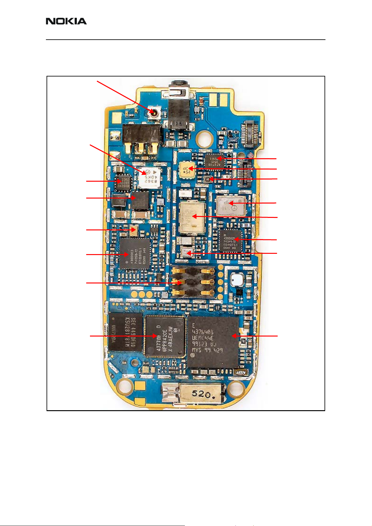
Mobile Terminal Components
Figure 1 illustrates the main components of the 2355.
RF connector
Cell isolator
Rx IC
PA PMIC
DC-DC
converter
Cell duplexer
Cell Rx RF
SAW filter
Cell Tx PA
Cell Tx SAW
filter
Tx Up- converter
UIM card
UPP (BB)
RF IF CDMA filter
VCO
Rx Down- converter
VCTCXO
UEM (BB)
Figure 1: Component layout (bottom)
ISSUE 1 02/2006 ©2006 Nokia Corporation Company Confidential Page 3
Page 4

2355 (RM-121)
RF Description and Troubleshooting Nokia Customer Care
Preliminary RF Troubleshooting
The following sections identify steps to troubleshoot some common RF issues.
Mobile Terminal Cannot Make a Call
Verify the following items if the mobile terminal cannot make a call:
1. The mobile terminal is in Normal Mode (i.e., the mobile terminal is searching for
a signal, net server is on).
2. The Preferred Roaming List (PRL) is loaded into the mobile terminal.
3. The mobile terminal is tuned and has passed tuning. Read the tuning parameters
using the Batch Tune component in Phoenix. An untuned mobile terminal has all
zeros in the tuning file.
4. The call box channel is set for a channel in PRL.
5. The SID is correct and entered into the mobile terminal.
6. The VCTCXO is centered as described in "VCTCXO Manual Tuning" on page 33
7. The transmitter and receiver are working properly in Local Mode. See
Tx Power Low
Complete the following steps if Tx power is low:
1. Use Phoenix to turn on the transmitter in Local Mode.
2. Perform a visual inspection of the PWB under a microscope to check for the
3. Look for the presence of a Tx signal on a spectrum analyzer at the correct
"Transmitter Troubleshooting" on page 8 and "Receiver
Troubleshooting" on page 16 for detailed information.
proper placement, rotation, and soldering of components.
frequency.
• If a signal is present but off-frequency, check the synthesizers for proper
frequency and amplitude. One of the synthesizers may be unlocked or the
VCO has no output signal.
• If a signal is not present or is present but is low in amplitude, check the
probing diagrams to determine where in the chain the fault occurs.)
4. Ensure that the power supplies to the Tx have the correct voltage.
5. Ensure that the AGC PDMs are set for the desired Tx power and that the AGC
voltages are correct.
Page 4 ©2006 Nokia Corporation Company Confidential ISSUE 1 02/2006
Page 5
2355 (RM-121)
Nokia Customer Care RF Description and Troubleshooting
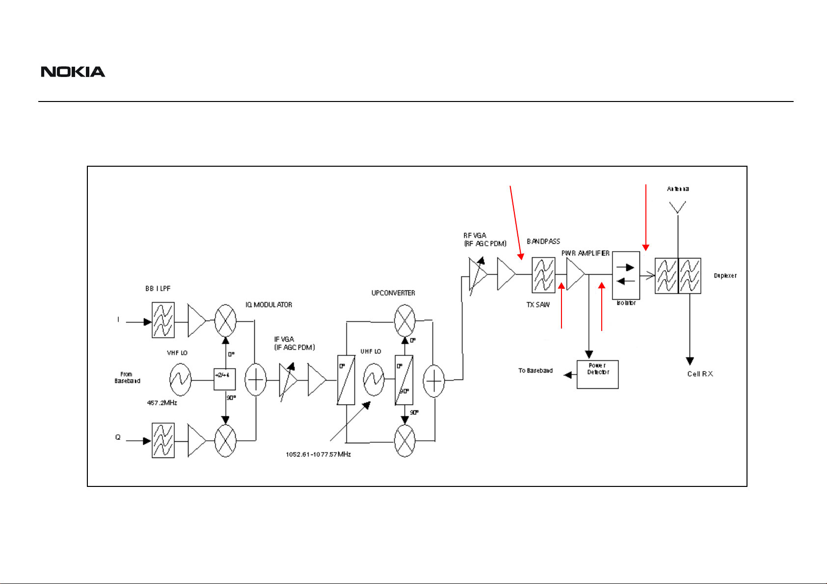
Transmitter Block Diagram
Following is the block diagram for the Tx RF system. I
TP1
TP4
TP2 TP3
Figure 2: Tx system block diagram
ISSUE 1 02/2006 ©2006 Nokia Corporation Company Confidential Page 5
Page 6
2355 (RM-121)
Nokia Customer Care RF Description and Troubleshooting
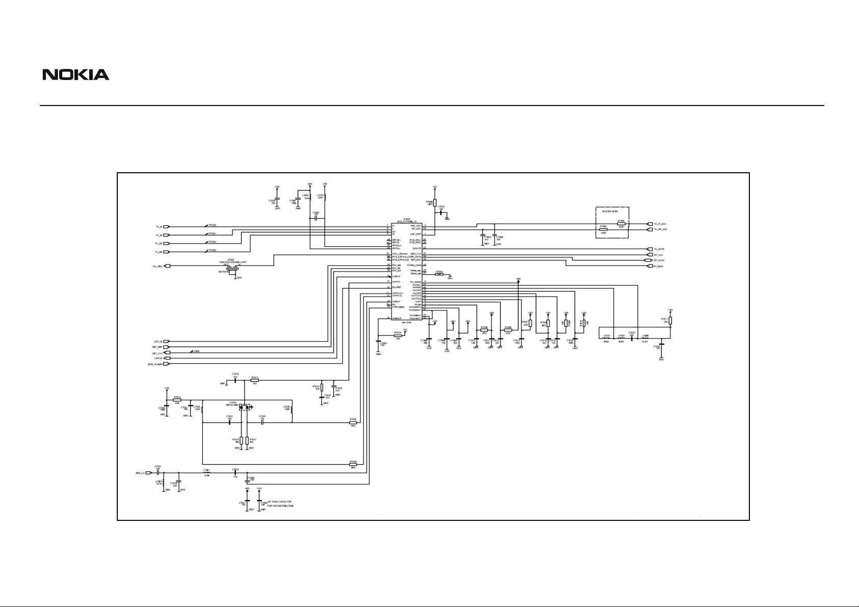
Transmitter Schematics
The following schematics are for general reference only. See the Schematics chapter for detailed versions.
Figure 3: Transmitter schematic 1
ISSUE 1 02/2006 ©2006 Nokia Corporation Company Confidential Page 6
Page 7
2355 (RM-121)
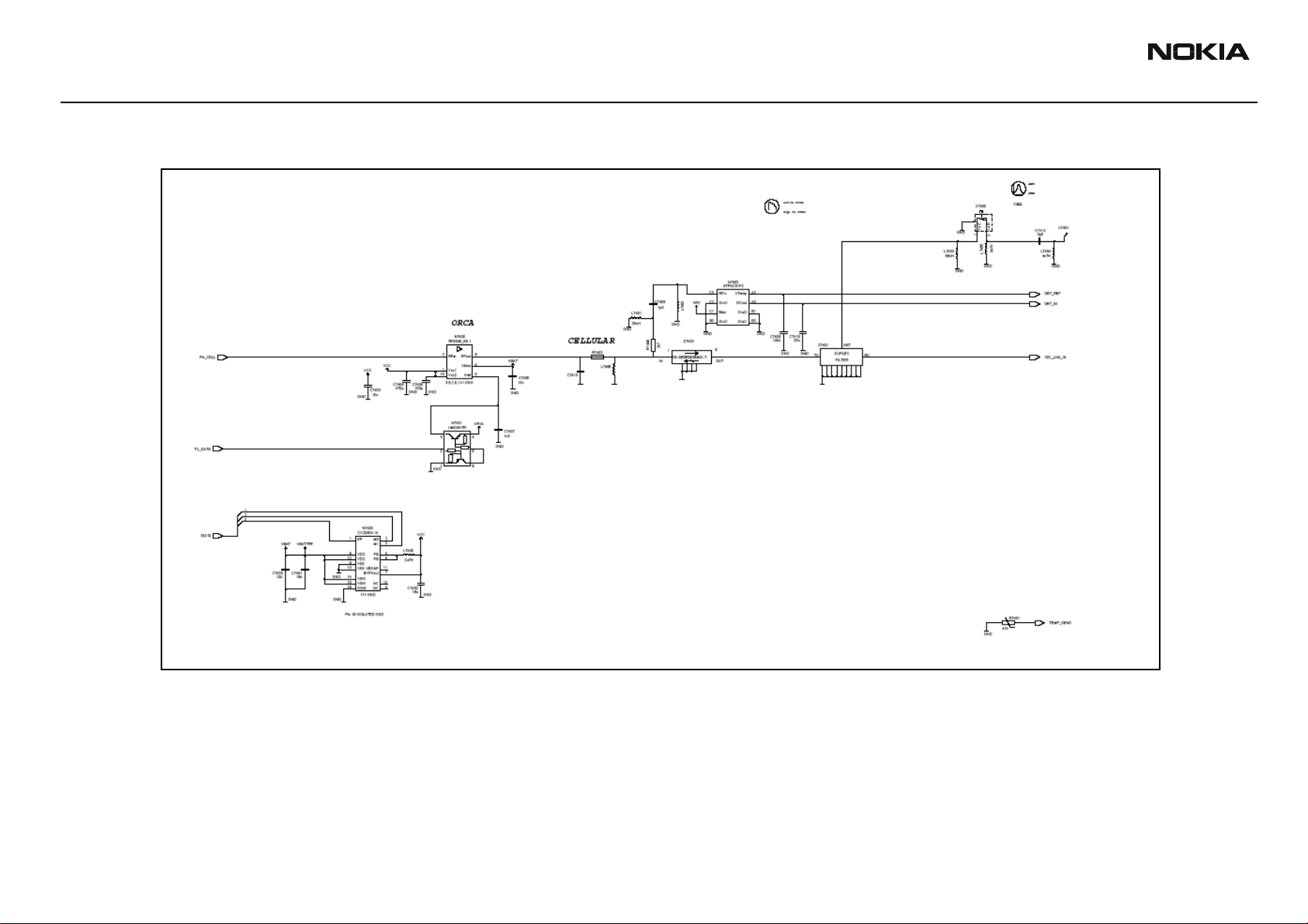
RF Description and Troubleshooting Nokia Customer Care
Figure 4: Transmitter schematic 2
Page 7 ©2006 Nokia Corporation Company Confidential ISSUE 1 02/2006
Page 8
2355 (RM-121)
RF Description and Troubleshooting Nokia Customer Care
Transmitter Troubleshooting
CELL Tx Setup
Use the following procedures to prepare for CELL Tx troubleshooting using Phoenix.
1. Connect RF test connector to a call box.
2. Connect the phone to a PC using the dummy battery adapter, and connect a
power supply.
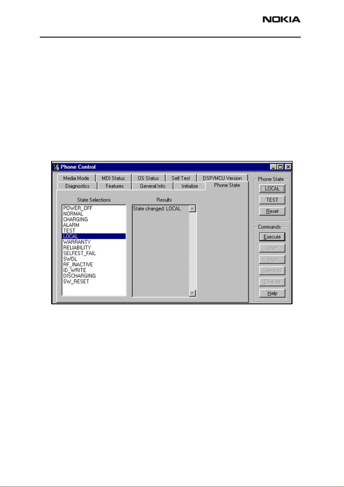
3. Open the Troubleshooting menu, and click Phone Control.
The Phone Control dialog box appears.
4. On the Phone Control dialog box, click the LOCAL button in the Phone State
area to put the phone into Local Mode.
Figure 5: Phone Control dialog box
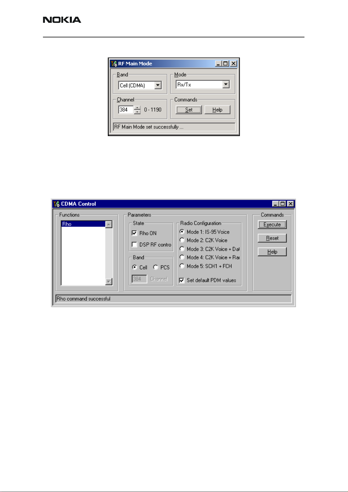
5. Open the Troubleshooting menu, point to RF, and click CDMA Control. The RF
Main Mode dialog box appears.
6. Select the following values on the RF Main Mode dialog box:
• Band = Cell (CDMA)
• Channel = 384
• Mode = Rx/Tx
Page 8 ©2006 Nokia Corporation Company Confidential ISSUE 1 02/2006
Page 9
2355 (RM-121)
Nokia Customer Care RF Description and Troubleshooting
Figure 6: RF Main Mode dialog box
7. Click Set.
Note: Be sure that the “RF Main Mode set successfully” message appears in the status bar.
8. Open the Troubleshooting menu, point to RF, and click CDMA Control.
The CDMA Control dialog box appears.
Figure 7: CDMA Control dialog box for Cell Tx troubleshooting
9. Select the following values on the CDMA Control dialog box.
• State = Rho ON
• Band = Cell
• Radio Configuration = Mode 1: IS-95 Voice
• Select the Set default PDM values check box.
10. Click Execute.
11. At this point you should be able to measure Tx Pout at the RF connector. The cell
band Tx Pout = 0 to 2 dBm. If you do not see these values, set the AGC PDM for
25 dBm and probe the Tx path to figure out where in the path the fault occurs.
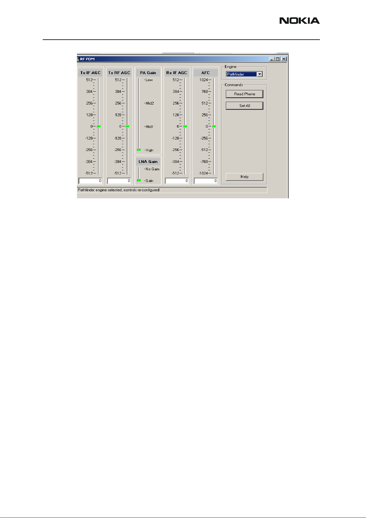
12. Open the Troubleshooting menu, point to RF, and click PDM Control.
The RF PDM Control dialog box appears.
ISSUE 1 02/2006 ©2006 Nokia Corporation Company Confidential Page 9
Page 10
2355 (RM-121)
RF Description and Troubleshooting Nokia Customer Care
Figure 8: RF PDM Control dialog box for Cell troubleshooting
13. Click Read Phone to update the values.
14. Configure the spectrum analyzer using the following values:
• Center Frequency = 836.52 MHz
• Span = 100 MHz
• RF LVL Amplitude = 20 dBm
• Attenuation = Auto
• BW = Auto
Adjust the following PDM field values on the RF PDM dialog box:
• Set PA Gain State to High
• Adjust Tx RF AGC PDM to around –250
• Adjust Tx IF AGC PDM to around –250
• Set Output level to +23dBm on CH-384 and monitor the current between
590mA and 660mA.
Failed Test: Tx PA Detector
1. Use Phoenix to set the phone in Local Mode, and activate the Tx with default
output power. The output power at the RF test connector should read
9 dBm +/- 4 dB.
2. Use a voltmeter on DC, and probe the detector output at C813. The voltmeter
should read approximately 1.4 V. If not, replace the detector (N803).
Page 10 ©2006 Nokia Corporation Company Confidential ISSUE 1 02/2006
Page 11
2355 (RM-121)
Nokia Customer Care RF Description and Troubleshooting
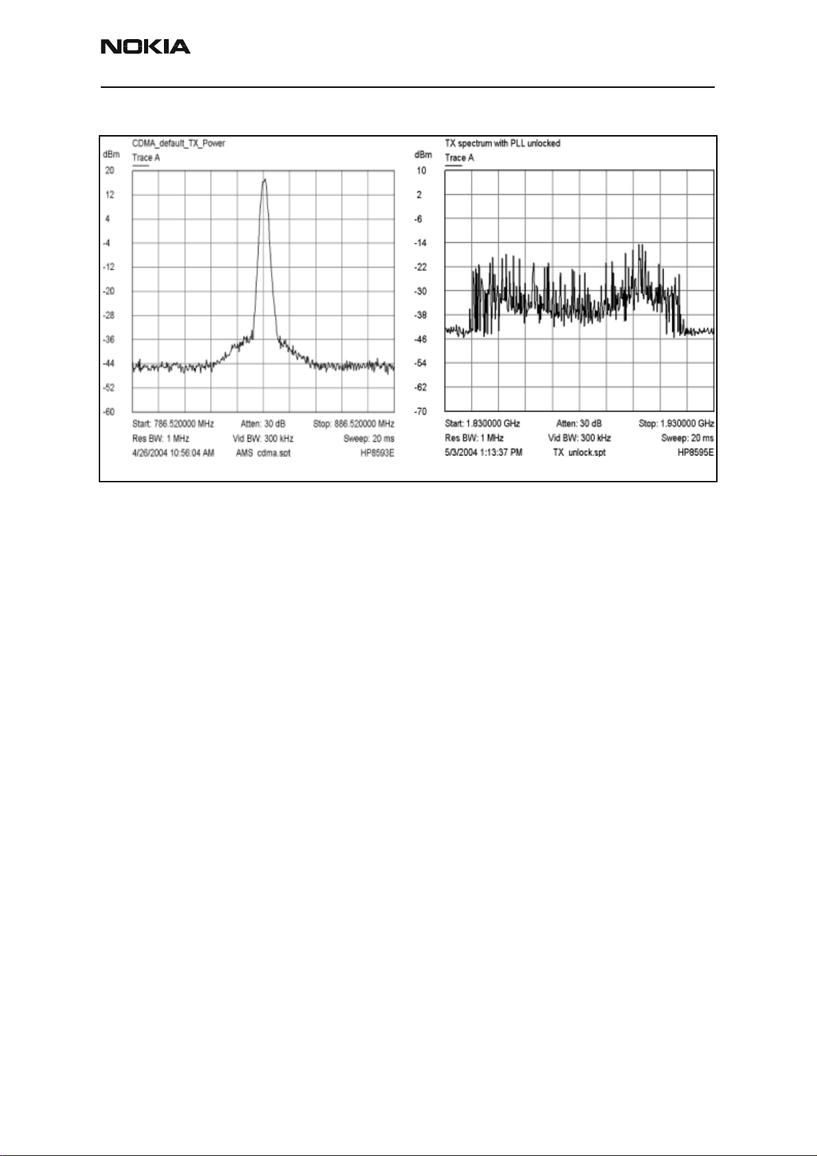
Good output
Figure 9: The output of the mobile terminal on a spectrum analyzer should look like the figure on the left
Bad output
If using the AAS-10 probe with the phone connected to the call box, the amplitude
should be approximately -7 dBm at the antenna test point on the top of the PWB.
ISSUE 1 02/2006 ©2006 Nokia Corporation Company Confidential Page 11
Page 12
2355 (RM-121)
RF Description and Troubleshooting Nokia Customer Care
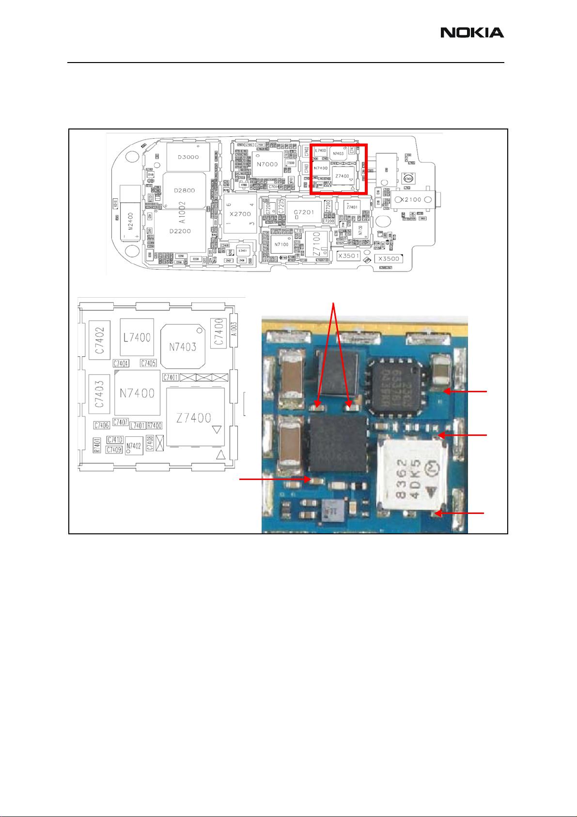
Tx RF Test Points
Figure 10 and Figure 11 are the transmitter DC/RF test points. See Table 1 on page 14 for
test point descriptions and values.
214
9
3
TP12
PNMIC
DC-DC
TP11
TP13
Figure 10: Tx DC/RF test points - PA section
TP3
TP4
Page 12 ©2006 Nokia Corporation Company Confidential ISSUE 1 02/2006
Page 13
2355 (RM-121)
Nokia Customer Care RF Description and Troubleshooting
Following are the Tx DC/RF test points for the N7000 Tx Section
214
3
TP5
TP91
TP6
TP10
TP7
TP9
N7000 Tx
Figure 11: Tx DC/RF test points - N7000 section
Tx SAW
TP2
TP3
TP8
ISSUE 1 02/2006 ©2006 Nokia Corporation Company Confidential Page 13
Page 14
2355 (RM-121)
RF Description and Troubleshooting Nokia Customer Care
Table 1 shows the Tx DC/RF test points to probe (see Figure 10 and Figure 11) when
troubleshooting the cell transmitter path. It is recommended that you follow the steps in
order.
Table 1: Tx DC test points
Typical Value/
Test Point FUnction
Frequency
HP85024A
TP1 Z7000
pin 1
TP2 Z7000
pin 3
TP3 Z7400
In
TP4 Z7400
Out
TP5 C7002 IF - Out -29 dBm/ 1MHz
TP6 VR5 2.75V dc VHF VCO/PLL, IQ modulator
TP7 VR7 2.75V dc UHF PLL supply from UEM
TP8 VR2 2.75V dc Mixer, driver, and IF supply
N7000 - Out -40 dBm/ 1MHz
836.52MHz
PA - In -26 dBm/ 1MHz
836.52MHz
PA - Out 5.0 dBm/ 1MHz
836.52MHz
Iso - Out 2.5 dBm/ 1MHz
836.52MHz
228.6MHz
Typical Value/
Frequency
Prod Probe
-13.2dBm/
836.52MHz
-15.4 dBm/
836.52MHz
18.3 dBm/
836.52MHz
10.3 dBm/
836.52MHz
-24 dBm/
228.6MHz
Comments
Output of N7000 Driver,
Input to Tx SAW Filter
Output of Tx SAW,
Input to PA
Input to Isolator
Output of Isolator,
Input to Duplexer
Tx IF probing point at IF
filter
supply from UEM
from UEM
TP9 R7002
TP91 R7001
TP10 VIO-Tx 1.8V Supply for digital circuits
TP11 VBAT 3.2V dc Battery voltage (nominal
TP12 VCC 3.1V dc (High Gain) Main PA supply voltage
TP13 C7407 VG/Vref 4.6V dc (Enable) PA gate voltage (Enable/
VAGC-RF
VAGC-IF
0.2 to 1.8V dc Tx AGC control voltage
from UPP.
0.2V = Max Gain
1.8V = Min Gain
from UEM
voltage 3.7V dc)
from PMIC.
Lgain=0.8V, Mgain=1.25V,
Hgain=Vbat
Disable). Disable=0V
Page 14 ©2006 Nokia Corporation Company Confidential ISSUE 1 02/2006
Page 15

2355 (RM-121)
Nokia Customer Care RF Description and Troubleshooting
Tx AGC Tuning
Tx power versus IF/RF PDM can be verified against FlaLi specification limits. Make sure
that the PA is set in high gain mode (GenIO bits 10, 13, and 12 are set to H).
Table 2: Tx AGC Tuning Steps
Tx Tuning
AGC Step
Tx AGC (0) -46 -55 -37
Tx AGC (1) -24 -34 -14
Tx AGC (2) -15 -25 -6
Tx AGC (3) -4.5 -14 5
Tx AGC (4) 2.5 -7 12
Tx AGC (5) 6 -3 15
Tx AGC (6) 15 6 24
Tx AGC (7)* 25 21 27
*Not an actual FlaLi tuning PDM. PDM produces approx. 25 dBm at the antenna connector.
Target
Power
Low
Limit
High
Limit
ISSUE 1 02/2006 ©2006 Nokia Corporation Company Confidential Page 15
Page 16

2355 (RM-121)
÷
Nokia Customer Care RF Description and Troubleshooting
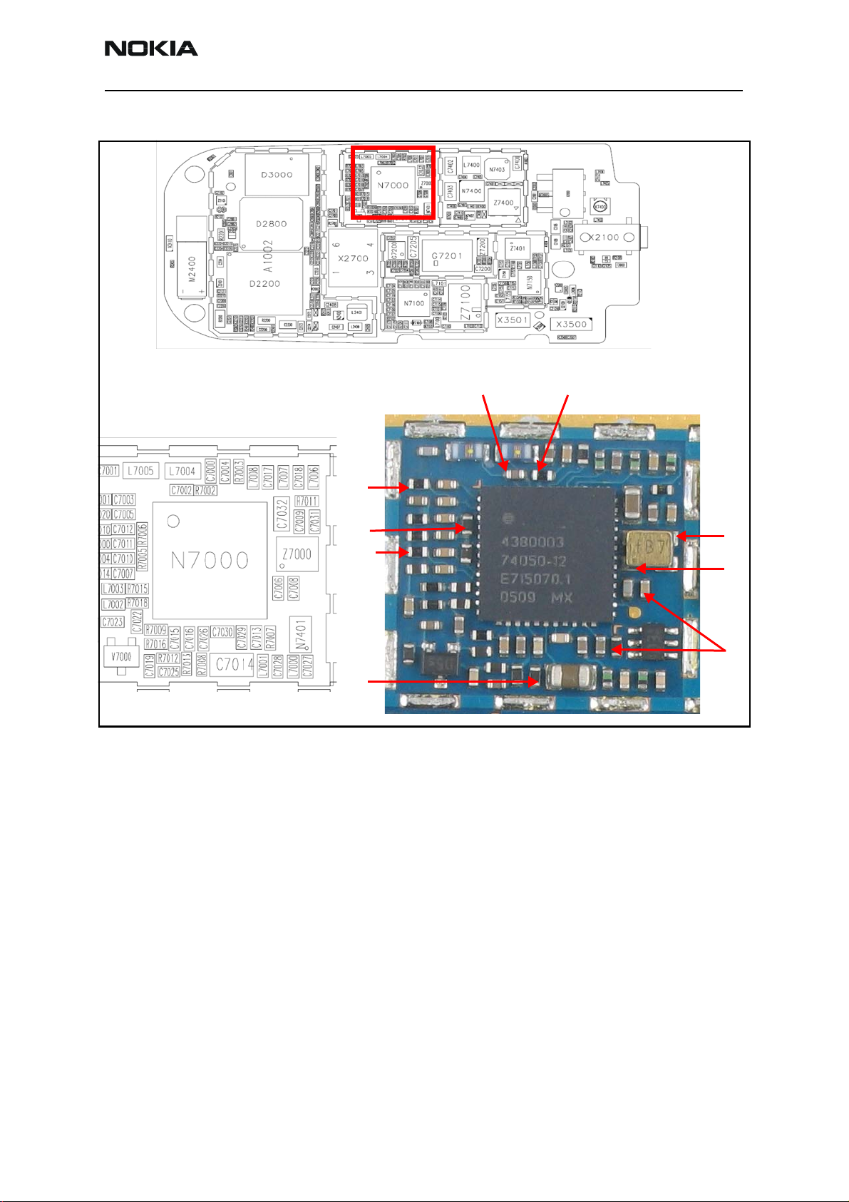
Receiver Troubleshooting
Following is the Rx system block diagram.
LNA SW Control
Duplexer
TX
Antenna
LNA
CELL
SAW
Loop Filter
N7160 IC N7100 IF IC
VGA
RFA
IFA
IF SAW
I/Q Down
Converter
CDMA
BB Filter
BB AMP
CDMA
BB Filters
BB AMP
2
UHF VCO
1052.61-1077.57
Reference Clock
UHF Synthsizer
JEDI
VCTCXO
To BB
VHF PLL
367.2 MHz
Bias and Control
To Base-Band
AFC
Figure 12: Receiver system block diagram
ISSUE 1 02/2006 ©2006 Nokia Corporation Company Confidential Page 16
Page 17

2355 (RM-121)
RF Description and Troubleshooting Nokia Customer Care
Receiver Schematics
The following schematics are for general reference only. See the Schematics chapter for detailed versions.
LNA Input
RF SAW filter
Mixer Output 183.6 MHz
LNA Gain Control
CDMA IF Out 183.6 MHz
Lo in
Figure 13: Receiver schematic 1
Page 17 ©2006 Nokia Corporation Company Confidential ISSUE 1 02/2006
Page 18

2355 (RM-121)
Nokia Customer Care RF Description and Troubleshooting
.
Figure 14: Receiver schematic 2
ISSUE 1 02/2006 ©2006 Nokia Corporation Company Confidential Page 18
Page 19

2355 (RM-121)
Nokia Customer Care RF Description and Troubleshooting
Turning on the Rx Path
Use the following steps to turn on the Rx path using Phoenix.
1. Turn on Receiver Only in CDMA mode.
2. On the Phone Control dialog box, click the LOCAL button in the Phone State
area to put the phone into Local Mode.
Figure 15: Phone Control dialog box
3. Click Execute.
4. On the RF Main Mode dialog box select the following values:
• Band = Cell (CDMA)
• Channel = 384
• Mode = Rx
5. Click Set.
Figure 16: RF Main Mode dialog box for Cell Mode
Note: Be sure that the “RF Main Mode set successfully” message appears in the status bar
ISSUE 1 02/2006 ©2006 Nokia Corporation Company Confidential Page 19
Page 20

2355 (RM-121)
RF Description and Troubleshooting Nokia Customer Care
Switching the Rx Gain, IF, and IP States
Use the RF Gen I/O dialog box to switch the gain state (Hi and Lo) for CDMA mode.
Select the desired state, and click Refresh.
• Lo Gain Mode: Move the green square to No Gain.
• High Gain Mode: Move the green square to Gain.
MIN MIN
MAX MAX
Figure 17: RF Main Mode dialog box for Cell Switching Rx Gain States
Page 20 ©2006 Nokia Corporation Company Confidential ISSUE 1 02/2006
Page 21

2355 (RM-121)
Nokia Customer Care RF Description and Troubleshooting
Receiver Troubleshooting
Use Phoenix to perform the following steps for troubleshooting the receiver. Together
with the VCO frequency and level verification, this test should be the first test for a
non-working receiver. This test verifies the entire receiver chain, from input connector to
baseband output.
1. Open the Phone Control dialog box.
Figure 18: Phone Control dialog box for Rx IF troubleshooting
2. Click the LOCAL button in the Phone State area to put the mobile terminal into
Local Mode.
3. Select the following values on the RF Main Mode dialog box:
• Band = Cell (CDMA)
• Channel = 384
• Mode = Rx
Figure 19: RF Main Mode dialog box for Rx IF troubleshooting
4. Click Set.
Note: Be sure that the “RF Main Mode set successfully” message appears in the status bar.
ISSUE 1 02/2006 ©2006 Nokia Corporation Company Confidential Page 21
Page 22

2355 (RM-121)
RF Description and Troubleshooting Nokia Customer Care
5. Use a Spectrum analyzer to test TP3 (I+,I-, Q+, Q-), Set the S.A to 300KHz Center
Frequency, 200KHz SPAN and +10dBm Reference level
6. See Figure 20. For the first two tests (Tp1,Tp2), inject CW signal at 881.52 MHz
(CH-384) at a fixed –25dBm Power level (Same as for the RF tests).
7. Using Phoenix, set the Receiver to Rx mode, High Gain, Ch-384, same as in the
RF section.
Receiver RF Troubleshooting Test Points
TP9
Figure 20: Receiver Rx troubleshooting test points
Page 22 ©2006 Nokia Corporation Company Confidential ISSUE 1 02/2006
Page 23

2355 (RM-121)
Nokia Customer Care RF Description and Troubleshooting
]
TP9
Figure 21: Receiver Rx troubleshooting test points
ISSUE 1 02/2006 ©2006 Nokia Corporation Company Confidential Page 23
Page 24

2355 (RM-121)
RF Description and Troubleshooting Nokia Customer Care
Receiver IF Troubleshooting Test Points
4
TP9
TP3
TP6
Figure 22: Receiver IF troubleshooting test points
Page 24 ©2006 Nokia Corporation Company Confidential ISSUE 1 02/2006
Page 25

2355 (RM-121)
Nokia Customer Care RF Description and Troubleshooting
4
Figure 23: Receiver IF troubleshooting test points
ISSUE 1 02/2006 ©2006 Nokia Corporation Company Confidential Page 25
Page 26

2355 (RM-121)
RF Description and Troubleshooting Nokia Customer Care
Cell Receiver Check from RF to IQ
Use the following values to check the CDMA Cell Rx functionality from RF to IQ output.
1. Start Phoenix in Local Mode with only the Rx path turned on.
2. Inject a –75dBm CW signal for Cell 881.82MHz or 881.22 (CH-384 offset by
300KHz from 881.52MHz or 10 channels away).
3. Measure a 300kHz tuning on the analyzer. You should see a typical -21dBm IQ
tuning for CDMA Cell.
Figure 24 shows the Cell spectrum with an inject tone at -75dBm, as well as the IQ
output test points. Note that DC is present on the IQ output test points, and all test
points should be approximately equal.
CH394
CH394
881.82MHz
881.82MHz
Rx IP
Rx IN
300kHz
300kHz
+615kHz-615kHz
CH384
CH384
881.52MHz
881.52MHz
Figure 24: Cell spectrum (left) and IQ output test points (right)
+615kHz-615kHz
Rx QN
Rx QP
Page 26 ©2006 Nokia Corporation Company Confidential ISSUE 1 02/2006
Page 27

2355 (RM-121)
m
Nokia Customer Care RF Description and Troubleshooting
Cell I Q Output
dBm
0
-10
-20
-30
-40
-50
-60
-70
-80
Trace A
1
Trace A
302 kHz
1
-21.2500 dB
-90
-100
Centre: 300 kHz Span: 200 kHzAtten: 10 dB
Res BW: 3 kHz Vid BW: 3 kHz Sweep: 100 ms
5/5/2004 3:29:30 PM HP8595ECellIQ.spt
Figure 25: Receiver IQ level on CDMA Cell band
Receiver Diagnostic using Signal Tracing and Call Box
Use the following steps to trace a receiver signal. Refer to diagrams above.
1. Inject an external signal source of –25dBm into the RF input. An Agilent call box
8960 is recommended.
2. Press the Call Setup button, press the Active Cell soft button, and select CW.
3. Inject a CW signal for Cell 881.82MHz or 881.22 (CH-384 offset by 300KHz) at a
fixed –75dBm power level.
ISSUE 1 02/2006 ©2006 Nokia Corporation Company Confidential Page 27
Page 28

2355 (RM-121)
RF Description and Troubleshooting Nokia Customer Care
Rx Front-End IC (N7150) DC Troubleshooting
There are two common explanations for an N7150 failure consisting of high current in
Local Mode with just the Rx turned on:
• No presence of an LO signal
• Input impedance drop shorting out one of the DC supply pins to the chip.
IMPORTANT: You must check for both conditions before replacing the chip. If you
have no LO signal, refer to "Synthesizer Troubleshooting" on page 28. If you have a
significant supply voltage drop on one of the supply pins, then replace the N7150..
Table 3: N7150 Conditions and Supply Currents
Condition: Local Mode, Set
Rx Only in RF Main Mode
Good mobile terminal 100mA
No UHF LO signal present 254mA
Pin 13 shorted 255mA
Synthesizer Troubleshooting
Faulty synthesizers can cause both Rx and Tx failures during tuning, in addition to the
VCTCXO tuning. The following synthesizers are used in the 2255:
• UHF (CELL) PLL inside N7000 IC.
• Tx VHF (457.2MHz) with PLL in N7000 IC.
• Rx VHF (367.2MHz) with PLL in N7100 IC.
Supply Current
(From Power Supply)
Page 28 ©2006 Nokia Corporation Company Confidential ISSUE 1 02/2006
Page 29

2355 (RM-121)
Nokia Customer Care RF Description and Troubleshooting
Synthesizer Block Diagram
CELL:457.2MHz
CELL:457.2MHz
JEDI
JEDI
367.2MHz
367.2MHz
VHF
VHF
counter
counter
Yoda
Yoda
19.2MHz
19.2MHz
VCTCXO
VCTCXO
19.2MHz to
19.2MHz to
UPP
UPP
VHF
VHF
counter
counter
UHF
UHF
counter
counter
Figure 26: Synthesizer block diagram
CELLl Band UHF VCO
CELLl Band UHF VCO
ISSUE 1 02/2006 ©2006 Nokia Corporation Company Confidential Page 29
Page 30

2355 (RM-121)
RF Description and Troubleshooting Nokia Customer Care
Synthesizer Schematic
The following schematic is for general reference only. See the Schematics chapter for detailed versions.
VCTCXO with AFC control
19.2MHz buffer not installed
VCO
UHF PLL IC
Loop filter
Figure 27: Synthesizer schematic
Page 30 ©2006 Nokia Corporation Company Confidential ISSUE 1 02/2006
Page 31

2355 (RM-121)
Nokia Customer Care RF Description and Troubleshooting
Synthesizer Troubleshooting Setup
Use the following steps to troubleshoot the synthesizer using Phoenix:
1. On the Phone Control dialog box, click the LOCAL button in the Phone State
area to put the phone into Local Mode.
Figure 28: Phone Control dialog box
2. Use the following settings for the Band, Channel, and Mode fields on the RF
Main Mode dialog box:
• UHF: Use the Rx/Tx mode and channel 384 in Cell band. This allows you to
check power in both the Rx and Tx circuits.
• Rx VHF: Use the Rx mode. One band is enough.
• Tx VHF: Use the Rx/Tx mode in Cell band.
3. Click Set.
Note: Be sure that the “RF Main Mode set successfully” message appears in the status bar.
4. Read register templates N7000 (0) bits 10 and 11 for the UHF and Tx VHF lock
condition
ISSUE 1 02/2006 ©2006 Nokia Corporation Company Confidential Page 31
Page 32

2355 (RM-121)
RF Description and Troubleshooting Nokia Customer Care
Figure 29: RF Register R/W dialog box for synthesizer setup
5. Read register templates N7100 (0) bit 11 for the Rx VHF lock condition.
Page 32 ©2006 Nokia Corporation Company Confidential ISSUE 1 02/2006
Page 33

2355 (RM-121)
Nokia Customer Care RF Description and Troubleshooting
19.2 MHZ VCTCXO Reference Clock
To N7000 PLL
19.2MHz @ -24dBm w/production probe
-14dBm w/HP probe (20dB pad)
VCTCXO
Figure 30: 19.2 MHz VCTCXO Reference clock
To N7100/BB
19.2MHz @ -24dBm
(CLK19M2_R)
VCTCXO Manual Tuning
1. The VCTCXO can be manually tuned to verify failed tuned phones, or to verify if a
phone cannot make a call. This can be done with the phone in Local Mode and
generating a CW signal. The frequency accuracy of the VCTCXO can be measured
using an HP8960 callbox in AMPS mode, an HP4406 Tx tester, or a spectrum
analyzer (preferably using a lab system 10MHz source as equipment reference).
Replace the VCTCXO if the VCTCXO AFC DAC value does not meet the tuning
requirements after tuning.
ISSUE 1 02/2006 ©2006 Nokia Corporation Company Confidential Page 33
Page 34

2355 (RM-121)
RF Description and Troubleshooting Nokia Customer Care
Figure 31: 19.2 MHz VCTCXO reference clock
Pwerform the following steps to set up a CW signal:
1. Open the Phone Control dialog box.
Figure 32: Phone Control dialog box for VCTCXO troubleshooting
2. Click the LOCAL button in the Phone State area to put the phone into Local
Mode.
Page 34 ©2006 Nokia Corporation Company Confidential ISSUE 1 02/2006
Page 35

2355 (RM-121)
Nokia Customer Care RF Description and Troubleshooting
3. Select the following values on the RF Main Mode dialog box:
• Band = Cell (CDMA)
• Channel = 384
• Mode = Rx/Tx
Figure 33: RF Main Mode dialog box for VCTCXO troubleshooting
Change to
GenIO Output
and set to High
4. Do not use CDMA control to turn on Rho.
5. Open the BB General I/O dialog box to set the CW signal.
6. Type 10, 13, 12, and 8 in the fields in the PIN # column.
Figure 34: General I/O dialog box for VCTCXO tuning
7. Click the Get All button.
8. Change the value for Pin 8 in the Source column to GenIO Output.
9. Ensure that all of the pins have a value of H in the State column. (Click the L
values to change them to H values.)
ISSUE 1 02/2006 ©2006 Nokia Corporation Company Confidential Page 35
Page 36

2355 (RM-121)
RF Description and Troubleshooting Nokia Customer Care
10. The next step depends on the type of measurement equipment you are using:
• HP4406 or a spectrum analyzer: Set the center frequency to 836.52MHz and
the span to 2MHz. Also, establish a marker at 836.52MHz.
• HP8960: Set the callbox state to AMPS, and set the channel to 384. Use the
Frequency Accuracy measurement to center the VCTCXO.
11. Adjust the AFC value to center the VCTCXO on the RF PDM dialog box. The
tuning range is approximately +/- 10kHz..
Adjust AFC to
center
VCTCXO
manually
Figure 35: Manually adjusting the AFC to center VCTCXO
12. Adjust the AFC value so that the output signal is within +/- 100Hz. If you are
using an HP4406 or a spectrum analyzer, narrow the span to 1kHz or less.
If the VCTCXO does not tune, replace the UEM.
13.
Page 36 ©2006 Nokia Corporation Company Confidential ISSUE 1 02/2006
Page 37

2355 (RM-121)
Nokia Customer Care RF Description and Troubleshooting
UHF Synthesizer Test Points
Figure 36 shows the UHF Synthesizer layout.
1
19.2MHz VCTCXO UHF VCO LO coupler
Loop filter
components
Lock voltage probe point:
DC between 1 and 2 V
Figure 36: UHF Synthesizer test points
7
N7000 LO/PLL Input
Match Components
RF test point, Tx LO output levels:
CELL CH 384: 1065.12MHz @ –17dBm
With production probe
-26dBm w/HP probe (20dB pad)
ISSUE 1 02/2006 ©2006 Nokia Corporation Company Confidential Page 37
Page 38

2355 (RM-121)
RF Description and Troubleshooting Nokia Customer Care
UHF Synthesizer Schematic
The following schematic is for general reference only. See the Schematics chapter for a detailed version.
LO to Rx
LO to Tx/PLL
UHF VCO
Loop filter components Lock voltage (1to 2V)
N7000 LO input matching
components
Figure 37: UHF synthesizer schematic
N7000 Tx LO input
N7000 PLL input
(PLL in N7000 IC)
Page 38 ©2006 Nokia Corporation Company Confidential ISSUE 1 02/2006
Page 39

2355 (RM-121)
Nokia Customer Care RF Description and Troubleshooting
Incorrect UHF Frequency
Following are possible causes for incorrect UHF frequencies:
• Power supplies to PLL N7000 missing or low (VR7)
• Loop filter components missing or incorrectly installed
• Matching components to N7000 TxLO/PLL input missing or incorrectly installed
• 19.2MHz reference clock missing or low
• Programming is incorrect
• Component failure (VCO or PLL portion of N7000)
Rx VHF
Figure 38 shows the Rx VHF test points layout.
N7100 IC with
Integrated PLL
Lock voltage test point
DC voltage between
1V and 2 V
RF test point:
367.2MHz @ -61 dBm
With Production probe
-1 dBm with HP Probe.
Figure 38: Rx VHF test points
ISSUE 1 02/2006 ©2006 Nokia Corporation Company Confidential Page 39
Page 40

2355 (RM-121)
RF Description and Troubleshooting Nokia Customer Care
Rx VHF Schematic
The following partial schematic is for general reference only. See the Schematics chapter
for a detailed version.
PLL in N7100
Resonator
Loop filter
Lock voltage
components
Incorrect Rx VHF Frequency
Following are possible causes for incorrect Rx VHF frequencies:
• Power supplies to PLL portion of IC N7100 missing or low (VR7)
• Loop filter or resonator components missing or incorrectly installed
• 19.2MHz reference clock missing or low
• Programming is incorrect
Figure 39: Rx VHF schematic
Page 40 ©2006 Nokia Corporation Company Confidential ISSUE 1 02/2006
Page 41

2355 (RM-121)
Nokia Customer Care RF Description and Troubleshooting
Tx VHF
Figure 38 shows the Tx VHF test points layout
N7000 IC with
Integrated VHF PLL
Lock voltage
test point
DC voltage between 1 and 2 V
RF test point:
CELL: 457.2 MHZ @ -18.7dBm
With production probe
-19dBm w/HP probe (20dB pad)
Figure 40: Tx VHF test points
ISSUE 1 02/2006 ©2006 Nokia Corporation Company Confidential Page 41
Page 42

2355 (RM-121)
RF Description and Troubleshooting Nokia Customer Care
Tx VHF Schematic
The following partial schematic is for general reference only. See the Schematics chapter for a detailed version.
Lock voltage
Loop filter
N7000
Resonator
Figure 41: Tx VHF schematic
Page 42 ©2006 Nokia Corporation Company Confidential ISSUE 1 02/2006
Page 43

2355 (RM-121)
Nokia Customer Care RF Description and Troubleshooting
Incorrect Tx VHF Frequency
Following are possible causes for incorrect Tx VHF frequencies:
• Power supplies to PLL portion of IC N7000 missing or low (VR5)
• Loop filter or resonator components missing or incorrectly installed
• 19.2MHz reference clock missing or low
• Programming is incorrect
• Component failure (N7000 IC)
ISSUE 1 02/2006 ©2006 Nokia Corporation Company Confidential Page 43
Page 44

2355 (RM-121)
RF Description and Troubleshooting Nokia Customer Care
FM Radio Troubleshooting
Figure 42 shows the FM Radio layout. FM Radio circuits are located on the top of the
PWB.
Figure 42: FM Radio layout
FM Radio Troubleshooting Setup
Use the following steps to troubleshoot the FM radio while using universal headset to
the UHJ connector.
1. Connect the universal headset (HS-9) to the UHJ connector (top connector).
2. Select the Menu > Media > Radio from the mobile terminal user interface.
3. Set a local radio channel by selecting “Automatic tuning” from the Radio menu and
scanning up and down by pressing the “Up” and “Down” key respectively.
4. Listen for sound coming from the headset.
• If a signal is present the radio is functioning properly.
• If no channel can be found or no static/sound inspect all FM radio baseband
Page 44 ©2006 Nokia Corporation Company Confidential ISSUE 1 02/2006
Page 45

2355 (RM-121)
Nokia Customer Care RF Description and Troubleshooting
and audio circuits. Refer to the “Audio” section of the Baseband Description
and Troubleshooting chapter for more information.
Inspect visually for
open connections
or shorts.
Figure 43: FM Radio Module
ISSUE 1 02/2006 ©2006 Nokia Corporation Company Confidential Page 45
Page 46

2355 (RM-121)
RF Description and Troubleshooting Nokia Customer Care
This page intentionally left blank.
Page 46 ©2006 Nokia Corporation Company Confidential ISSUE 1 02/2006
 Loading...