

Page 1
After Sales Technical Documentation
HANDSFREE DESKTOP
CHARGER
CHH–7
Original, 11/94 NMP Part No. 0275012
Page 2
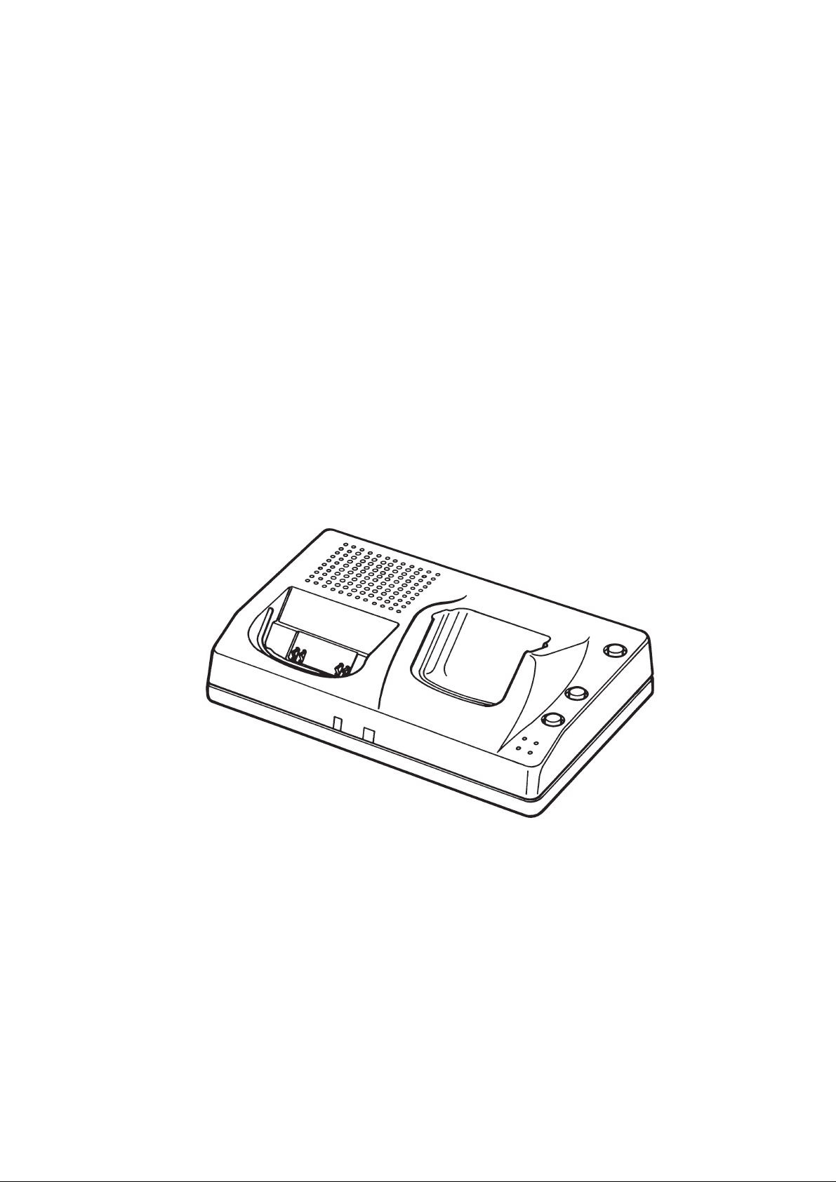
Handsfree Desktop Charger CHH–7
AMENDMENT RECORD SHEET
After Sales
Technical Documentation
Amendment
Number
Date Inserted By Comments
Original, 11/94Page 2
Page 3

After Sales
Technical Documentation
Handsfree Desktop Charger CHH–7
HANDSFREE DESKTOP CHARGER CHH–7
CONTENTS
Page No
Introduction 5
Technical Summary 5
Operation 5
List of Modules 5
Basic Specifications 6
Technical Specifications 6
Modes of Operation 6
DC Characteristics 7
AC Characteristics 8
External Signals and Connections 9
Internal Signals and Connections 11
Mechanical Characteristics 12
User Interface Features 12
Charge States and Charge Control 13
Charge Indication to User 13
Environmental Conditions 15
Temperature Conditions 15
Functional Description 16
Circuit Description (DC3H) 18
Control Logic 18
Watchdog Function 21
Switch Mode Power Supply (SMPS) 21
Battery Charging 21
Spare Battery Discharging 22
Microphone Amplifier and Corresponding Switches 22
Speaker Amplifier and Corresponding Switches 22
Circuit Description (DC4H) 22
Original, 11/94 Page 3
Page 4

Handsfree Desktop Charger CHH–7
Technical Documentation
Assembly 23
DC3H ModuleParts List 24
DC4H Module Parts List 32
After Sales
List of Figures
Figure 1: Block Diagram 16
Figure 2: Component Location Diagram 17
Figure 3: Exploded View 23
Figure 4: DC3H Circuit Diagram (Sheet 1) 33
Figure 5: DC3H Circuit Diagram (Sheet 2) 34
Figure 6: DC4H Circuit Diagram (Sheet 3) 35
Original, 11/94Page 4
Page 5
After Sales
Technical Documentation
Introduction
The CHH–7 Handsfree Desktop Charger provides both charging and
handsfree facilities. The charger enables a phone plus a spare battery to
be charged; the spare battery is charged after the phone battery has been
charged. CHH–7 can only be powered by the AC Power Supply
(ACS–6U/X/E); the supply is connected to the charger via a socket at the
rear of the charger.
Analogue data accessories may be used in conjunction with the
Handsfree Desktop Charger; a connector at the rear of the charger is
provided for this purpose.
The BABT approved version of CHH–7 is known as CHH–7X. Since both
units are technically identical, all references to CHH–7 equally apply to
CHH–7X.
Handsfree Desktop Charger CHH–7
Technical Summary
Operation
CHH–7 consists of a spare battery charging control processor, charging
indicators and a switched mode power supply for charging the phone and
the spare battery. The unit has an in–built hf–speaker and hf–microphone
but the handsfree function is generated in the phone. There are also
three operating buttons: the front one is a MUTE button for the CHH–7
microphone; the middle one is for redialling the last number dialled; and
the rear one is for selecting the spare battery discharge.
List of Modules
Table 1. List of Modules
NAME OF MODULE TYPE
CODE
HF Deskstand Charger CHH–7 0675040 Fully Assembled Charger
HF Desktop Charger and
Connector Module
HF Desktop Charger DC3H 0200334 Main Electronic Components and Connector
DCXH 0200335 A single PCB biscuit containing both the HF Desktop
MATERIAL
CODE
NOTES
Charger and Connector Module
Connector Module DC4H 0200295 System Connectors, Data Buffer and Noise Comp
Assembly Parts MCHH7 0260338 Mechanical Parts,Speaker, Microphone and Flex Foils
Original, 11/94 Page 5
Page 6
Handsfree Desktop Charger CHH–7
Basic Specifications
Table 2. Basic Specifications
Power Consumption 13W max.
Input Voltage Range 13.5V to 21.0V
After Sales
Technical Documentation
Battery Charger: Output Voltage
Output Current
Maximum Charging Time (empty battery): BTH–8S (400mAh): 45min
Maximum Discharging Time (full battery): BTH–8S (400mAh): 3h 30min
Operating Temperature +5C to +55C
Charging Temperature +5C to +45C (40C when fitting battery)
Speaker Output Power nominal: 1W / 8ohm
External Main Dimensions 43mm (H) x 167mm (W) x 113mm (D)
Weight 360g
10.0V to 13.0V
730mA to 870mA
BTH–8H (500mAh): 55min
BTH–8SM (800mAh): 70min
BTH–8HM (1100mAh): 100min
BTH–8H (500mAh): 4h 20min
BTH–8SM (800mAh): 7h
BTH–8HM (1100mAh): 8h 40min
NOTE: To ensure the battery is fully charged, it is recommended to
continue charging for 2 to 3 hours after a fast charge has
been completed.
Technical Specifications
Modes of Operation
Power Off Mode: The unit receives no power at the DC–
connector.
Standby Mode: The unit receives the supply voltage at
the DC–connector. The processor is
running but because there isn’t a phone
or spare battery in the cradle, the
charger remains off and the audio
functions are inactive.
Active Mode: The telephone or spare battery is in the
cradle so the charging functions are
active. Normally the handsfree speaker
is muted. During a call and during the
key beeps or alarming tones the
speaker and corresponding audio
switches are open.
Original, 11/94Page 6
Page 7
After Sales
Technical Documentation
DC Characteristics
Table 3. Supply Voltages and Power Consumption on the Connectors of CHH–7
Handsfree Desktop Charger CHH–7
CONNECTOR
Pin/Connector
DC
1 / X100
SPARE
BATTERY
X101, X102
X103, X104
SYSTEM
10 / X701
DATA Analogue
2 / X510
Table 4. Supply Voltages and Power Consumptions on the DC3H–module
SYMBOL/
MODULE
+VI Power Supply 13.5V 13.8V 21.0V
+VCC Charging voltage for the
+10VA Supply for logic and
+10VAS Switched supply for logic
+5V Supply for logic
+5VREF Reference voltage for uP 4.9V 5.0V 5.1V
+5VLD Supply voltage for LEDs 4.9V 5.0V 5.1V
+5VAN Supply for analogue parts 4.6V 5.0V 5.1V
+VAREF Reference voltage for
LINE SYMBOL MINIMUM TYPICAL/
VDC
Input Voltage
Input Power
VBAT
Charging:
Output Voltage
Output Current
Discharging:
Input Voltage
Input Current
VC
Charging:
Output Voltage
Output Current
VD
Output Voltage
Output Current
PARAMETER MINIMUM TYPICAL/
battery
analogue parts
and analogue parts
parts
analogue parts
13.5V 13.8V 21.0V
11.0V
730mA
5.0V
130mA
11.0V
730mA
9.6V 10.0V 10.4V
10.3V
730mA
9.6V 10.0V 10.4V
9.1V 9.8V 10.2V
4.9V 5.0V 5.1V
2.2V 2.5V 2.7V
NOMINAL
12.2V
800mA
6.0V
160mA
12.2V
800mA
NOMINAL
11.5V
800mA
MAXIMUM
13.0W
13.0V
870mA
7.5V
200mA
13.0V
870mA
50.0mA
MAXIMUM
13W
13.3V
870mA
250mA
250mA
35mA
1.5mA
30mA
1mA
0.1mA
Original, 11/94 Page 7
Page 8
Handsfree Desktop Charger CHH–7
AC Characteristics
Table 5. External Microphone signal
XMIC (1 kHz) TYPICAL/NOMINAL
After Sales
Technical Documentation
Cable level
0 dBmO
Table 6. Handsfree Microphone Signal
HFMIC (1 kHz) TYPICAL/NOMINAL
MRP +15.3dBPa / 50 cm (Mic Ref Point)
HFMIC input –4.7dBPa (approx 20dB attenuation)
Gain for HFMIC 40dB
Cable Level 200mV
Table 7. External Earphone Signal
XEAR (1 kHz) TYPICAL/NOMINAL
Cable Level
0 dBmO
200mV
415mV
130mV
411mV
Table 8. Handsfree Speaker Signal
HFSP (1kHz) TYPICAL/NOMINAL
Cable Level 130mV
Gain for HFSP 23dB
Table 9. Audio Specifications
f = 1 kHz MINIMUM TYPICAL/NOMINAL MAXIMUM
HF Microphone Sensitivity (0dB = 1V/Pa) –44dB –42dB –40dB
Sending Idle Noise –61dBmO
HF Speaker: SPL (1W @ 1m) +78dB +80dB +82dB
Receiving Idle Noise –52dBPa (A)
Speaker Output Power 1W/8Ω
Original, 11/94Page 8
Page 9
After Sales
Handsfree Desktop Charger CHH–7
Technical Documentation
External Signals and Connections
Table 10. List of External Connectors
CONNECTOR MODULE NOTES DESCRIPTION
SYSTEM DC4H CHH–7 <–––> Phone 10 connections
SP ARE BATTERY DC3H CHH–7 <–––> Spare Battery 4 contact springs
DATA DC3H CHH–7 <–––> Data Accessory 10 pins modular connector
DC DC3H CHH–7 <–––> Power Supply 6.3 mm DC–Jack
Table 11. DC Connector X100
PIN LINE/
SYMBOL
1 VDC Supply voltage
Supply power
2 DGND Power supply ground 0V 0V 0V
CONTACT/
SPRING
X104 GND Supply power ground 0V 0V 0V
X103 BTEMP Battery temp sensing 2.47V
X102 BSI Battery size
X101 VBAT Charging voltage
LINE/
SYMBOL
PARAMETER MINIMUM TYPICAL/
NOMINAL
13.5V 13.8V 21.0V
Table 12. Spare Battery Connector X101, ....X104
PARAMETER MINIMUM TYPICAL/
NOMINAL
613mV (400mAh)
identification.
Charging current
11V
730mA
764mV (500mAh)
1.53V (800mAh)
2.29V (1100mAh)
12V
800mA
MAXIMUM
13.0W
MAXIMUM
13V
870mA
Table 13. System Connector X701
PIN LINE
SYMBOL
5 GND Power supply ground 0V 0V 0V
9 XMIC Microphone signal
8 AGND analogue ground 0V 0V 0V
7 M2BUS Serial bidirection data 0V
PARAMETER MINIMUM TYPICAL/
NOMINAL
200mV
dc–level
output impedance
3.0V
0V
3.6V
2.5V
MAXIMUM
700Ω
0.7V Input ”0” state
5.25V Input ”1” state
0.35V Output ”0” state
5.25V Output ”1” state
Original, 11/94 Page 9
Page 10
Handsfree Desktop Charger CHH–7
Table 13. System Connector X701 (continued)
After Sales
Technical Documentation
PIN
SYMBOL
3 HOOK Selects handsfree
operation
6 VC Supply / Charging 11V
10 GND Power supply ground 0V 0V 0V
4 XEAR /
HFJPWR
1 VC Supply / Charging 11V
2 XEXAUD Not used
PIN LINE
SYMBOL
2 +VD Supply voltage
3 DGND Supply power ground 0V 0V 0V
Earphone signal
dc–level
input impedance 10kΩ
CHH–7 power switch 5.0V (power off)
Table 14. Data Connector X510
PARAMETER MINIMUM TYPICAL/
Supply current
MINIMUMPARAMETERLINE
NOMINAL
0V 0V 0V
12V
730mA
730mA
9.6V 10.0V 10.4V
800mA
130mV
2.5V
2.5V (power on)
12V
800mA
NOMINAL
13V
830mA
0.8V (test mode for
power off watch–dog)
13V
870mA
50mA
MAXIMUMTYPICAL/
MAXIMUM
4 M2BUS Serial bidirection data 0V
3.0V
0V
3.6V
1, 5 Not Used
6 Not Used
7 AGND analogue ground 0V 0V 0V
8 XMIC Microphone signal
dc–level
output impedance
9 XEAR Earphone signal
dc–level
input impedance 10kΩ
0.2V
4.7V
200mV
2.5V
130mV
2.5V
0.7V Input ”0” state
5.25V Input ”1” state
0.35V Output ”0” state
5.25V Output ”1” state
700Ω
Original, 11/94Page 10
Page 11

After Sales
Handsfree Desktop Charger CHH–7
Technical Documentation
Internal Signals and Connections
Table 15. List of Internal Connectors
CONNECTOR MODULE NOTES DESCRIPTION
Internal System
Connector
Spare Battery
Connector
Speaker Connector DC3H X460 <––> Hf–speaker 2 connections, wires
Microphone
Connector
Table 16. Internal System Connectors X500 / DC3H and X700 / DC4H
PIN
AT
X700
1
2
5 M2BUS Serial bidirection data 0V
8 AGND analogue ground 0V 0V 0V
7 XEAR Earphone signal
6 AGND analogue ground 0V 0V 0V
LINE
SYMBOL
VC Supply / Charging 11V
DC3H/
DC4H
DC3H X101...X104 <––> Battery Conn. Contact Springs
DC3H X440 <––> Hf–microphone 2 connections, wires
PARAMETER MINIMUM TYPICAL/
dc–level
input impedance 10kΩ
DC3H: X500 <–> DC4H: X700 10 connections, flex foil
NOMINAL
730mA
3.0V
0V
3.6V
12V
800mA
130mV
2.5V
13V
830mA
0.7V Input ”0” state
5.25V Input ”1” state
0.35V Output ”0” state
5.25V Output ”1” state
MAXIMUM
9 XMIC Microphone signal
dc–level
output impedance
10 AGND analogue ground 0V 0V 0V
3
4
PIN LINE
1 HFSPK HF Speaker Signal
2 AGND analogue Ground 0V 0V 0V
DGND Power supply ground 0V 0V 0V
Table 17. Speaker Connector X460 / DC3H
PARAMETER MINIMUM TYPICAL/NOMINAL MAXIMUM
SYMBOL
Load Impedance
Output Power
200mV
2.5V
700Ω
2.83V
8Ω
1W
Original, 11/94 Page 11
Page 12

Handsfree Desktop Charger CHH–7
Table 18. Microphone Connector X440 / DC3H
After Sales
Technical Documentation
PIN LINE
SYMBOL
1 HFMIC HF Microphone
2 AGND analogue ground 0V 0V 0V
PARAMETER MINIMUM TYPICAL/NOMINAL MAXIMUM
Output Voltage
(without load)
Input Impedance
4.7V
1.0kΩ
Mechanical Characteristics
Table 19. Mechanical Characteristics
UNIT DIMENSIONS (mm)
(W x H x D)
CHH–7: Colour: Warm Black
DCXH PCB
includes DC3H and DC4H
modules
flex foil 65 x 9 System connector flex
155 x 1.6 x 94.5 PCB has 6 layers / 1.6mm
WEIGHT
(g)
NOTES
DC4H–module: 50 x 1.6 x 22 PCB has 6 layers / 1.6 mm
User Interface Features
Charging takes place at a battery temperatures of between 5 and 45.
Control of the charging process for the phone is performed by a
microprocessor located inside the phone; control of the charging process
for the spare battery is performed by a separate microprocessor located in
the HF desktop charger. The phone is always charged first, followed by
the spare battery. When a spare battery is fitted, the temperature must be
less than 40
A battery provides a larger capacity if it is occasionally discharged
completely. The user can do this by using the ‘deep discharge‘ feature.
This feature only operates with the spare battery slot. With the battery
located in the spare slot, the spare battery will automatically be
discharged and then re–charged to full capacity when the ‘discharge‘
–button is depressed. If this button is pressed twice the discharge
function is cancelled.
Original, 11/94Page 12
Page 13

After Sales
Technical Documentation
Charge States and Charge Control
Charge current for the phone is supplied through a series connected
switching transistor located in the phone. When this transistor is on, the
charger is supplying a constant current to the phone. This is the rapid
charge mode.
When the transistor is off, no current is supplied to the phone and the
charger is in the constant voltage mode.
Having been charged up in the rapid charge mode, the battery is kept fully
charged by using pulsed charging, ie. switching power alternately on and
off at a variable duty cycle and a frequency of a few Hz.
The desktop charger also contains control logic for spare battery charging,
which is enabled when no phone is connected or when the phone is in the
pulsed charge mode. When the phone is in pulse charge mode the spare
battery can only be charged at 70% of the rate when no phone is present.
Handsfree Desktop Charger CHH–7
Charge Indication to User
The desktop charger has dual–colour LEDs to indicate the charge state of
the phone and the spare battery, the right hand LED is for the phone and
the left hand LED is for the spare battery. The LEDs are off when there is
no phone or spare battery connected.
Right LED for phone:
Red phone LED indicates that the phone battery is being charged in fast
charge mode or charging is disabled due to battery temperature being
outside permissible range.
Green phone LED indicates that the phone battery is full and that trickle
charge mode is active.
Left LED for spare battery:
Red spare battery LED indicates that the battery is not full; either there is
a fast charge mode active or charging is disabled due to a battery
temperature ’fault’ or the phone is being fast charged.
Green spare battery LED indicates that the battery is fully charged.
Flashing red spare battery LED indicates that a discharge cycle is active.
The liquid–crystal display of the phone also contains a three–bar battery
charge display. ”Charging sequence active” (state A) is indicated by the
bars illuminated sequentially, starting from the bottom bar (each bar is on
for a period of 1 s).
”Battery full” (state B) is indicated by all three bars steadily illuminated.
Original, 11/94 Page 13
Page 14

Handsfree Desktop Charger CHH–7
Technical Documentation
Table 20. Phone Operating Status
PHONE OPERA TING STA TUS RIGHT HAND LED PHONE DISPLAY
After Sales
Desktop charger connected to mains
through ac adapter, phone
disconnected
Rapid charge or waiting for the
right temperature (+5C to +45C)
Battery full – trickle charge green state B (all bars steadily
Table 21. Spare Battery Operating Status
SPARE BATTERY OPERATING STATUS LEFT HAND LED
Desktop charger connected to mains through ac adapter, spare battery
disconnected
Rapid charge of spare battery or waiting for the phone charging ready or for
the right temperature
Spare battery full – trickle charge green
Discharge of spare battery flashing red
– –
red state A (bars illuminated
sequentially)
illuminated)
–
red
Handsfree Function
When located in the charger, the phone always operates in handsfree
mode; the charger’s internal HF speaker and HF microphone being active
during the call. It is also possible to switch between handsfree and
handset operation while a call is in progress. This is done by removing
the phone from the charger (to return to handset operation) or placing it in
the charger (to return to handsfree operation).
The HF speaker volume is adjusted using the volume keys located on the
side of the phone. The HF volume level is set independently from the
phone’s internal earpiece volume; the HF volume setting is stored in the
phone’s memory when the phone is removed from the charger. The HF
microphone audio can be muted by pressing the mute key on the front
edge of the charger. The muted state is indicated by the message
”MUTE” appearing on the phone’s display. Pressing the ”MUTE” key a
second time cancels the mute function.
Original, 11/94Page 14
Page 15

After Sales
Technical Documentation
Environmental Conditions
Temperature Conditions
Table 22. Allowed Ambient Temperature
ENVIRONMENTAL PARAMETER VALUE
Handsfree Desktop Charger CHH–7
Operating Temperature
Storage Temperature
– 5 to + 55°C
(charging: + 5 to + 45°C)
– 40 to + 85°C
Original, 11/94 Page 15
Page 16

Handsfree Desktop Charger CHH–7
Functional Description
Figure 1: Block Diagram
DC CONNECTOR
CHARGER
After Sales
Technical Documentation
CHH–7
MODULE
PHONE
CHARGING
INDICATION
MODULE
SPARE BATTERY CONNECTOR
SPARE
BATTER Y
CHARGE /
DISCHARGE
CONTROL
BUTTONS
PROCESSOR
CHARGING LEDs
RFI
FILTER
COMP.
SYSTEM CONNECTOR
AUDIO
DATA CONNECTOR
SPEAKER HFMIC
Original, 11/94Page 16
Page 17

After Sales
Technical Documentation
Figure 2: Component Location Diagram
Handsfree Desktop Charger CHH–7
Original, 11/94 Page 17
Page 18

Handsfree Desktop Charger CHH–7
Circuit Description (DC3H)
The DC3H–Module consists of the following functional blocks:
– Supply Voltages
– Control Logic
– Battery Charging
– Spare Battery Discharging
– Watchdog Function
– Switch Mode Power Supply
– Microphone Amplifier and corresponding switches
– Speaker Amplifier and corresponding switches
After Sales
Technical Documentation
Refer to Figures 4 and 5 for DC3H circuit diagrams (sheets 1 and 2).
Control Logic
Charging is controlled by processor D300. The D300 is a single–chip type
controller incorporating RAM, ROM, an A/D converter, and a multifunction
timer/counter. The processor communicates with the phone via the
M2BUS. The M2BUS interface comprises transistors V200, V201 and
corresponding resistors.
Table 23. Port A Signals of the Processor:
PORT A NOTES
P A0: PHONE GREEN (output) Phone LED control, green: ”1”
P A1: PHONE RED (output) Phone LED control, red: ”1”
P A2: SP ARE GREEN (output) Spare battery LED control, green: ”1”
P A3: SPARE RED (output) Spare battery LED control, red: ”1”
P A4: DISCHARGE BUTTON (input) Discharge button control,
”0”: start / stop discharge
P A5: SP ARE DISCHARGE (output) Discharge spare battery ,
”1”: discharge enabled
PA6: Unused (output) Not Used
PA7: CHARGER (output) Charger Switch, ”1”: charger on
Original, 11/94Page 18
Page 19

After Sales
⇒ CHH–7
Handsfree Desktop Charger CHH–7
Technical Documentation
Table 24. Port B Signals of the Processor: (continued)
PORT B NOTES
PB0: SERVICE J301 (output) See next table
PB1: SERVICE J302 (output) See next table
PB2: SERVICE J303 (output) See next table
PB3: SERVICE J304 (output) See next table
PB4: SERVICE J305 (output) Not Used
PB5: LAST NUMBER REDIAL (input) Last Number Redial button, ”0”: activation
PB6: HFMIC MUTE (input) HF Microphone Muting, ”0”: activation
PB7: PHONE IDENTIFICATION(input) pulled up +5V (= state ”1”)
Table 25. Service Test Pins of Port B:
J304 J303 J302 J301 NOTES
0 0 0 1 Battery voltage hi limit reached
0 0 1 0 Maximum charge time
0 0 1 1 Voltage drop (delta V)
0 1 0 0 Battery temperature high
0 1 0 1 Constant voltage
Table 26. Port C Signals of the Processor:
PORT C NOTES
PC0: TXD (output) M2BUS Transmit
PC1: RXD (input) M2BUS Receive
PC2: Unused (input) Not Used
PC3: TRXDINT (input) M2BUS Interrupt
PC4: DVCE0 (input)
PC5: DVCE1 (input)
PC6: SP ARE CHARGE (output) Spare Battery Charging, ”1”: Charging on
Device Type ”1”
”
Device Type ”0”
”
PC7: WATCHDOG (output) Watchdog Reset, ”01010...”: Watchdog reset on
Original, 11/94 Page 19
Page 20

Handsfree Desktop Charger CHH–7
After Sales
Technical Documentation
Table 27. Port D Signals of the Processor:
PORT D NOTES
PD0: PHONE MIC (output) analogue Switch, ”1”: Phone mic switched on
PD1: ACC MIC (output) analogue Switch, ”1”: Accessory mic switched on
PD2: HF MIC (output) analogue Switch, ”1”: HF mic switched on
PD3: PHONE EAR (output) analogue Switch, ”1”: Phone ear switched on
PD4: ACC EAR (output) analogue Switch, ”1”: Accessory ear switched on
PD5: HF SPK (output) analogue Switch, ”1”: HF speaker switched on
PD6: Unused (output) Not Used
PD7: Unused (output) Not Used
Table 28. Port F Signals of the Processor:
PORT F NOTES
PF0: Unused (input) Not Used
PF1: Unused (input) Not Used
PF2: Unused (input) Not Used
PF3: Unused (input) Not Used
PF4: Unused (input) Not Used
PF5: Unused (input) Not Used
PF6: Unused (input) Not Used
PF7: Unused (input) Not Used
Table 29. Processor A/D Inputs:
NAME NOTES
AN0: VBATL Battery voltage
AN1: VBATH High resolution battery voltage
AN2: PHOCURDET Phone current detect
AN3: BATTEMP Battery temperature
AN4: BATTSZ Battery size
AN5: CHRGVOLT Charger voltage detection
AN6: PWR Phone connection detection
AN7: LIREF Not Used
Original, 11/94Page 20
Page 21

After Sales
Technical Documentation
Watchdog Function
Under normal operating conditions the processor is pulsating the
WATCHDOG–line in order to reset the power–off function of regulator
N102. If the processor is not functioning correctly and hence the regulator
does not send the pulse to the XPWROFF–line within the 100ms timeout
period, the regulator reverts to its power–off state resetting the processor
and switching the VAREF and +VAN voltages off. The regulator and the
processor can be restarted by pressing the discharge button (S300) once
or switching the power supply (connected to X100) off and on. The supply
voltage (+VA) for the regulator must be greater than 8.1V in order for the
regulator to switch on.
Switch Mode Power Supply (SMPS)
C100 and C101 are the EMI capacitors. L100 and L101 are EMI
suppressor chokes. V100 is the voltage suppressor (zener) diode.
Handsfree Desktop Charger CHH–7
The microprocessor D300 pin 2 starts the SMPS by starting reference
regulator N103. V115–1 leads the initial current to totally empty the
battery. V106 is a constant current source which sets the voltage value of
R118. The same voltage appears across the current shunt resistor R103
when the SMPS is working. N101–a is a pulse width modulator. N101–b,
together with R122, C103 and V114–1, generates a minimum pulse width.
R127 and R521 are input and output voltage correction resistors. V103
limits the comparator power supply +VS. V115–2 and V372 limits the
comparator output voltage. V341–1 and C341 form a bootstrap circuit,
which acts like a voltage doubler and generates the positive gate voltage
to switch the fet V102 gate. L111 (L109), R130 and C340 are
EMI–suppression components. L108 is the main SMPS inductor. V110
limits the maximum output voltage.
Battery Charging
Charging current for the phone battery is supplied when the processor
switches the SMPS on after the phone is connected to the system
connector X701 on the DC4H module. The charger voltage should be
between 13.5V and 21.0V. The phone battery’s charging state is indicated
by the red (V344 / V345) and green (V333) LEDs. Because the phone
and the spare battery cannot be charged simultaneously, the charging
current of the phone must be detected: this is achieved by a differential
amplifier (N250–A) and corresponding resistors.
Charging current for the spare battery is fed in via switching transistor
V221 and Schottky diode V220. The transistor is controlled by the
processor. When the phone battery is not being charged and hence the
spare battery is allowed to charge, the transistor is on and a constant
current is supplied to the battery (the red LED V331 lights). In the pulsed
charging mode, charging current is adjusted by pulsing this charge current
(the green LED V330 lights).
Original, 11/94 Page 21
Page 22

Handsfree Desktop Charger CHH–7
Spare battery voltage and V voltage are determined by reading the
VBAT line state. Voltages are measured through resistor divider R250 /
R251 and the amplifier N250–B.
Spare battery size is determined by reading the BSI line state. This is
pulled to the +5V reference voltage by R243. In the battery pack a ’size’
resistor is connected between BSI and GND.
Temperature is measured over the BTEMP line. This line is pulled to the
+5V reference voltage by R242. In the battery pack an NTC resistor is
connected between BTEMP and GND.
Spare Battery Discharging
The HF desktop charger is also provided with a discharge function. This
is activated by pressing the discharge button S300. Resistors R230 to
R237 determine the discharge current which is fed through switching
transistor V230 which is controlled by the processor. Discharging is
indicated by a flashing red LED (V331). The battery is discharged to +5V
and thereafter charged normally to full capacity.
After Sales
Technical Documentation
Microphone Amplifier and Corresponding Switches
Transistor amplifier circuit V420 and the corresponding resistors and
capacitors supply bias current for the microphone. Operational amplifier
N430–B amplifies the microphone signal before it is fed to the phone. The
gain of the op amp is approximately 38 dB.
The HF microphone signal is fed to the phone via analogue switches
D400–B and D400–C. The microphone signal XMIC, from the data
accessory (X510) is fed to the phone via switches D400–A and D400–C.
The supply voltage for the amplifier and the analogue switches is taken
from the +5VAN regulator N102. The +VAREF reference voltage is
derived from the N430–A and the +5VAN analogue voltage.
Speaker Amplifier and Corresponding Switches
The XEAR signal from the phone is fed to the HF speaker via analogue
switches D410–C and D410–B. The XEAR signal is amplified about 23dB
(+39dB via amplifier N460, –1dB via the analogue switches, and –15dB
via resistors R460 and R461). The XEAR signal from the phone can be
fed to data accessory (X510) via analogue switches D410–C and D410–A.
The supply voltage +10VAS for the speaker amplifier is derived from the
regulator N100.
Circuit Description (DC4H)
The DC4H–module electronics comprise noise reduction components
only. ’Spark gaps’ E1, E2, E4 and E8 protect against electrostatic
discharge. Refer to Figure 6 – Circuit Diagram (sheet 3).
Original, 11/94Page 22
Page 23

After Sales
Technical Documentation
Assembly
Figure 3: Exploded View
9
Handsfree Desktop Charger CHH–7
12
3X
1
2X
13
8
7
1
6X
14
10
6
15
11
16
3X
5
4
3
2
4X
ITEM 15
CHH–7X
ONLY
Original, 11/94 Page 23
Page 24

Handsfree Desktop Charger CHH–7
Technical Documentation
Assembly Parts
ITEM QTY CODE DESCRIPTION VALUE
1 8 6293012 Pt–Screw KB22x8 WN1442
2 4 6501067 Adhesive Foot D8.0
3 1 9450322 Bottom Cover D11403
4 1 5140444 Cond. Microphone 63 +/– 2dB
5 1 9460012 Microphone Pad 4D21140
6 1 7133160 Flex Foil 10x0.5, 0.8mm
7 1 5140460 Loudspeaker 8R 2W D=45
8 1 9460054 Speaker Seal Ring 3D22231
9 1 9560009 Ballast 4D23334
After Sales
H=19
10 1 9460088 Light Guide 3D22992
11 1 9450324 Front Cover D11402
12 3 9460087 Discharge Button 4D22992
13 1 9480052 Speaker Screen 4D22694
14 1 9380154 Type Label 4D22419
15 1 9380488 BABT Label (CHH–7X only) A12455
16 3 9560022 Spring (for buttons) 4D24399
DC3H Module Parts List
ITEM CODE DESCRIPTION VALUE TYPE
R100 1412279 Chip resistor 2.2 5 % 0.063 W 0805
R103 1411123 Melf resistor 0.22 5 % 0.2 W 0204
R116 1414452 Chip resistor 10.0 k 1 % 0.063 W 0805
R117 1413635 Chip resistor 100 k 5 % 0.063 W 0805
R118 1415600 Melf resistor 1.0 k 1 % 0.2 W 0204
R119 1412423 Chip resistor 4.7 k 5 % 0.063 W 0805
R120 1415784 Melf resistor 4.75 k 1 % 0.2 W 0204
R122 1413635 Chip resistor 100 k 5 % 0.063 W 0805
R123 1415600 Melf resistor 1.0 k 1 % 0.2 W 0204
R127 1414420 Chip resistor 680 k 5 % 0.063 W 0805
R130 1411669 Chip resistor 22 5 % 0.063 W 0805
R200 1412430 Chip resistor 10 k 5 % 0.063 W 0805
R201 1413635 Chip resistor 100 k 5 % 0.063 W 0805
R202 1412729 Chip resistor 33 k 5 % 0.063 W 0805
Original, 11/94Page 24
Page 25

After Sales
Technical Documentation
R203 1413635 Chip resistor 100 k 5 % 0.063 W 0805
R204 1412430 Chip resistor 10 k 5 % 0.063 W 0805
R205 1413917 Chip resistor 150 5 % 0.063 W 0805
R206 1413635 Chip resistor 100 k 5 % 0.063 W 0805
R209 1412423 Chip resistor 4.7 k 5 % 0.063 W 0805
R215 1412536 Chip resistor 22 k 5 % 0.063 W 0805
R216 1414533 Chip resistor 56 k 1 % 0.063 W 0805
R218 1412536 Chip resistor 22 k 5 % 0.063 W 0805
R219 1415632 Melf resistor 33.0 k 1 % 0.2 W 0204
R220 1413917 Chip resistor 150 5 % 0.063 W 0805
R221 1413917 Chip resistor 150 5 % 0.063 W 0805
R222 1413603 Chip resistor 47 k 5 % 0.063 W 0805
R223 1412423 Chip resistor 4.7 k 5 % 0.063 W 0805
R230 1415576 Melf resistor 301 1 % 0.2 W 0204
R231 1415576 Melf resistor 301 1 % 0.2 W 0204
R232 1415576 Melf resistor 301 1 % 0.2 W 0204
R233 1415576 Melf resistor 301 1 % 0.2 W 0204
R234 1415576 Melf resistor 301 1 % 0.2 W 0204
R235 1415576 Melf resistor 301 1 % 0.2 W 0204
R236 1415576 Melf resistor 301 1 % 0.2 W 0204
R237 1415576 Melf resistor 301 1 % 0.2 W 0204
R238 1412430 Chip resistor 10 k 5 % 0.063 W 0805
R240 1414533 Chip resistor 56 k 1 % 0.063 W 0805
R241 1414452 Chip resistor 10.0 k 1 % 0.063 W 0805
R242 1415664 Melf resistor 27.4 k 1 % 0.2 W 0204
R243 1414283 Chip resistor 100 k 1 % 0.063 W 0805
R244 1412423 Chip resistor 4.7 k 5 % 0.063 W 0805
R245 1413603 Chip resistor 47 k 5 % 0.063 W 0805
R246 1413603 Chip resistor 47 k 5 % 0.063 W 0805
R248 1416040 Melf resistor 56.2 k 1 % 0.2 W 0204
R249 1413603 Chip resistor 47 k 5 % 0.063 W 0805
R250 1416160 Melf resistor 100 k 1 % 0.2 W 0204
R251 1416202 Melf resistor 121 k 1 % 0.2 W 0204
R252 1416040 Melf resistor 56.2 k 1 % 0.2 W 0204
R253 1416160 Melf resistor 100 k 1 % 0.2 W 0204
R254 1413603 Chip resistor 47 k 5 % 0.063 W 0805
R255 1413603 Chip resistor 47 k 5 % 0.063 W 0805
R256 1414124 Chip resistor 120 k 5 % 0.063 W 0805
R257 1413635 Chip resistor 100 k 5 % 0.063 W 0805
R258 1412430 Chip resistor 10 k 5 % 0.063 W 0805
R300 1413635 Chip resistor 100 k 5 % 0.063 W 0805
R301 1412729 Chip resistor 33 k 5 % 0.063 W 0805
Handsfree Desktop Charger CHH–7
Original, 11/94 Page 25
Page 26

Handsfree Desktop Charger CHH–7
Technical Documentation
R302 1412423 Chip resistor 4.7 k 5 % 0.063 W 0805
R303 1412423 Chip resistor 4.7 k 5 % 0.063 W 0805
R304 1412423 Chip resistor 4.7 k 5 % 0.063 W 0805
R310 1413635 Chip resistor 100 k 5 % 0.063 W 0805
R311 1413635 Chip resistor 100 k 5 % 0.063 W 0805
R312 1413635 Chip resistor 100 k 5 % 0.063 W 0805
R313 1413635 Chip resistor 100 k 5 % 0.063 W 0805
R314 1412335 Chip resistor 1.0 k 5 % 0.063 W 0805
R315 1413635 Chip resistor 100 k 5 % 0.063 W 0805
R320 1414533 Chip resistor 56 k 1 % 0.063 W 0805
R321 1414283 Chip resistor 100 k 1 % 0.063 W 0805
R322 1413829 Chip resistor 10 5 % 0.063 W 0805
R323 1414283 Chip resistor 100 k 1 % 0.063 W 0805
R324 1414533 Chip resistor 56 k 1 % 0.063 W 0805
R330 1412536 Chip resistor 22 k 5 % 0.063 W 0805
R331 1412536 Chip resistor 22 k 5 % 0.063 W 0805
R332 1421108 Melf resistor 30.1 k 1 % 0.2 W 0204
R335 1412536 Chip resistor 22 k 5 % 0.063 W 0805
R336 1412536 Chip resistor 22 k 5 % 0.063 W 0805
R337 1412254 Chip resistor 270 5 % 0.063 W 0805
R338 1412198 Chip resistor 56 5 % 0.063 W 0805
R339 1412254 Chip resistor 270 5 % 0.063 W 0805
R341 1413635 Chip resistor 100 k 5 % 0.063 W 0805
R400 1413917 Chip resistor 150 5 % 0.063 W 0805
R401 1413635 Chip resistor 100 k 5 % 0.063 W 0805
R402 1413635 Chip resistor 100 k 5 % 0.063 W 0805
R403 1413635 Chip resistor 100 k 5 % 0.063 W 0805
R404 1413635 Chip resistor 100 k 5 % 0.063 W 0805
R405 1413635 Chip resistor 100 k 5 % 0.063 W 0805
R406 1413635 Chip resistor 100 k 5 % 0.063 W 0805
R410 1413635 Chip resistor 100 k 5 % 0.063 W 0805
R411 1413635 Chip resistor 100 k 5 % 0.063 W 0805
R412 1413917 Chip resistor 150 5 % 0.063 W 0805
R413 1413635 Chip resistor 100 k 5 % 0.063 W 0805
R414 1413635 Chip resistor 100 k 5 % 0.063 W 0805
R415 1413635 Chip resistor 100 k 5 % 0.063 W 0805
R416 1413635 Chip resistor 100 k 5 % 0.063 W 0805
R420 1414043 Chip resistor 1.8 k 5 % 0.063 W 0805
R421 1413635 Chip resistor 100 k 5 % 0.063 W 0805
R430 1412729 Chip resistor 33 k 5 % 0.063 W 0805
R431 1412729 Chip resistor 33 k 5 % 0.063 W 0805
R440 1413917 Chip resistor 150 5 % 0.063 W 0805
After Sales
Original, 11/94Page 26
Page 27

After Sales
Technical Documentation
R441 1413917 Chip resistor 150 5 % 0.063 W 0805
R442 1413603 Chip resistor 47 k 5 % 0.063 W 0805
R443 1414109 Chip resistor 15 k 5 % 0.063 W 0805
R444 1414109 Chip resistor 15 k 5 % 0.063 W 0805
R445 1412303 Chip resistor 330 5 % 0.063 W 0805
R446 1412729 Chip resistor 33 k 5 % 0.063 W 0805
R447 1413917 Chip resistor 150 5 % 0.063 W 0805
R460 1413603 Chip resistor 47 k 5 % 0.063 W 0805
R461 1414452 Chip resistor 10.0 k 1 % 0.063 W 0805
R462 1412423 Chip resistor 4.7 k 5 % 0.063 W 0805
R463 1413635 Chip resistor 100 k 5 % 0.063 W 0805
R464 1413850 Chip resistor 4.7 5 % 0.063 W 0805
R500 1412430 Chip resistor 10 k 5 % 0.063 W 0805
R500 1412729 Chip resistor 33 k 5 % 0.063 W 0805
R501 1412430 Chip resistor 10 k 5 % 0.063 W 0805
R501 1412729 Chip resistor 33 k 5 % 0.063 W 0805
R502 1413635 Chip resistor 100 k 5 % 0.063 W 0805
R520 1412423 Chip resistor 4.7 k 5 % 0.063 W 0805
R530 1413836 Chip resistor 47 5 % 0.063 W 0805
R532 1412286 Chip jumper 0805
R533 1413836 Chip resistor 47 5 % 0.063 W 0805
R534 1412303 Chip resistor 330 5 % 0.063 W 0805
C100 2310343 Ceramic cap. 22 p 5 % 50 V 0805
C101 2310343 Ceramic cap. 22 p 5 % 50 V 0805
C103 2309517 Ceramic cap. 100 n 10 % 50 V 1206
C104 2501605 Electrol. cap. 100 u 20 % 35 V RM3.5
C109 2501605 Electrol. cap. 100 u 20 % 35 V RM3.5
C110 2309517 Ceramic cap. 100 n 10 % 50 V 1206
C111 2502736 Electrol. cap. 220 u 20 % 16 V 3.5MM
C112 2502736 Electrol. cap. 220 u 20 % 16 V 3.5MM
C114 2310343 Ceramic cap. 22 p 5 % 50 V 0805
C115 2310752 Ceramic cap. 10 n 20 % 50 V 0805
C116 2604431 Tantalum cap. 10 u 20 % 16 V 6.0x3.2x2.8
C117 2604209 Tantalum cap. 1.0 u 20 % 16 V 3.2x1.6x1.8
C118 2604495 Tantalum cap. 22 u 20 % 16 V 7.3x4.4x2.8
C119 2310343 Ceramic cap. 22 p 5 % 50 V 0805
C120 2310343 Ceramic cap. 22 p 5 % 50 V 0805
C121 2310343 Ceramic cap. 22 p 5 % 50 V 0805
C122 2309517 Ceramic cap. 100 n 10 % 50 V 1206
C123 2307816 Ceramic cap. 47 n 20 % 25 V 0805
C124 2307816 Ceramic cap. 47 n 20 % 25 V 0805
C128 2310752 Ceramic cap. 10 n 20 % 50 V 0805
Handsfree Desktop Charger CHH–7
Original, 11/94 Page 27
Page 28

Handsfree Desktop Charger CHH–7
Technical Documentation
C129 2309884 Ceramic cap. 4.7 p 0.25 % 50 V 0805
C150 2310544 Ceramic cap. 1.0 n 5 % 50 V 0805
C151 2309517 Ceramic cap. 100 n 10 % 50 V 1206
C153 2604431 Tantalum cap. 10 u 20 % 16 V 6.0x3.2x2.8
C154 2604431 Tantalum cap. 10 u 20 % 16 V 6.0x3.2x2.8
C160 2310449 Ceramic cap. 150 p 5 % 50 V 0805
C210 2502736 Electrol. cap. 220 u 20 % 16 V 3.5MM
C211 2604209 Tantalum cap. 1.0 u 20 % 16 V 3.2x1.6x1.8
C212 2310343 Ceramic cap. 22 p 5 % 50 V 0805
C213 2310343 Ceramic cap. 22 p 5 % 50 V 0805
C220 2307816 Ceramic cap. 47 n 20 % 25 V 0805
C240 2307816 Ceramic cap. 47 n 20 % 25 V 0805
C241 2307816 Ceramic cap. 47 n 20 % 25 V 0805
C242 2307816 Ceramic cap. 47 n 20 % 25 V 0805
C243 2307816 Ceramic cap. 47 n 20 % 25 V 0805
C244 2309517 Ceramic cap. 100 n 10 % 50 V 1206
C250 2307816 Ceramic cap. 47 n 20 % 25 V 0805
C251 2307816 Ceramic cap. 47 n 20 % 25 V 0805
C252 2310449 Ceramic cap. 150 p 5 % 50 V 0805
C253 2307816 Ceramic cap. 47 n 20 % 25 V 0805
C300 2310343 Ceramic cap. 22 p 5 % 50 V 0805
C301 2310343 Ceramic cap. 22 p 5 % 50 V 0805
C302 2307816 Ceramic cap. 47 n 20 % 25 V 0805
C303 2307816 Ceramic cap. 47 n 20 % 25 V 0805
C310 2310343 Ceramic cap. 22 p 5 % 50 V 0805
C320 2307816 Ceramic cap. 47 n 20 % 25 V 0805
C340 2310544 Ceramic cap. 1.0 n 5 % 50 V 0805
C341 2309517 Ceramic cap. 100 n 10 % 50 V 1206
C341 2502736 Electrol. cap. 220 u 20 % 16 V 3.5MM
C342 2307816 Ceramic cap. 47 n 20 % 25 V 0805
C343 2310343 Ceramic cap. 22 p 5 % 50 V 0805
C400 2604209 Tantalum cap. 1.0 u 20 % 16 V 3.2x1.6x1.8
C401 2310488 Ceramic cap. 330 p 5 % 50 V 0805
C402 2604209 Tantalum cap. 1.0 u 20 % 16 V 3.2x1.6x1.8
C403 2604209 Tantalum cap. 1.0 u 20 % 16 V 3.2x1.6x1.8
C404 2604209 Tantalum cap. 1.0 u 20 % 16 V 3.2x1.6x1.8
C405 2307816 Ceramic cap. 47 n 20 % 25 V 0805
C410 2310343 Ceramic cap. 22 p 5 % 50 V 0805
C411 2604209 Tantalum cap. 1.0 u 20 % 16 V 3.2x1.6x1.8
C412 2604209 Tantalum cap. 1.0 u 20 % 16 V 3.2x1.6x1.8
C413 2604209 Tantalum cap. 1.0 u 20 % 16 V 3.2x1.6x1.8
C414 2604209 Tantalum cap. 1.0 u 20 % 16 V 3.2x1.6x1.8
After Sales
Original, 11/94Page 28
Page 29

After Sales
Technical Documentation
C415 2307816 Ceramic cap. 47 n 20 % 25 V 0805
C420 2310343 Ceramic cap. 22 p 5 % 50 V 0805
C421 2310343 Ceramic cap. 22 p 5 % 50 V 0805
C422 2310343 Ceramic cap. 22 p 5 % 50 V 0805
C423 2310343 Ceramic cap. 22 p 5 % 50 V 0805
C424 2604209 Tantalum cap. 1.0 u 20 % 16 V 3.2x1.6x1.8
C430 2307816 Ceramic cap. 47 n 20 % 25 V 0805
C431 2604209 Tantalum cap. 1.0 u 20 % 16 V 3.2x1.6x1.8
C432 2310343 Ceramic cap. 22 p 5 % 50 V 0805
C440 2310343 Ceramic cap. 22 p 5 % 50 V 0805
C441 2310752 Ceramic cap. 10 n 20 % 50 V 0805
C442 2604431 Tantalum cap. 10 u 20 % 16 V 6.0x3.2x2.8
C443 2310752 Ceramic cap. 10 n 20 % 50 V 0805
C444 2310343 Ceramic cap. 22 p 5 % 50 V 0805
C445 2310544 Ceramic cap. 1.0 n 5 % 50 V 0805
C446 2310343 Ceramic cap. 22 p 5 % 50 V 0805
C447 2310343 Ceramic cap. 22 p 5 % 50 V 0805
C448 2310544 Ceramic cap. 1.0 n 5 % 50 V 0805
C449 2310343 Ceramic cap. 22 p 5 % 50 V 0805
C450 2310343 Ceramic cap. 22 p 5 % 50 V 0805
C451 2604209 Tantalum cap. 1.0 u 20 % 16 V 3.2x1.6x1.8
C452 2310343 Ceramic cap. 22 p 5 % 50 V 0805
C460 2604209 Tantalum cap. 1.0 u 20 % 16 V 3.2x1.6x1.8
C461 2310738 Ceramic cap. 4.7 n 20 % 50 V 0805
C463 2604209 Tantalum cap. 1.0 u 20 % 16 V 3.2x1.6x1.8
C464 2310343 Ceramic cap. 22 p 5 % 50 V 0805
C465 2310343 Ceramic cap. 22 p 5 % 50 V 0805
C466 2310343 Ceramic cap. 22 p 5 % 50 V 0805
C467 2604431 Tantalum cap. 10 u 20 % 16 V 6.0x3.2x2.8
C468 2604431 Tantalum cap. 10 u 20 % 16 V 6.0x3.2x2.8
C469 2310343 Ceramic cap. 22 p 5 % 50 V 0805
C470 2502736 Electrol. cap. 220 u 20 % 16 V 3.5MM
C471 2310784 Ceramic cap. 100 n 10 % 25 V 0805
C472 2310343 Ceramic cap. 22 p 5 % 50 V 0805
C473 2309517 Ceramic cap. 100 n 10 % 50 V 1206
C500 2310343 Ceramic cap. 22 p 5 % 50 V 0805
C501 2310343 Ceramic cap. 22 p 5 % 50 V 0805
C510 2310343 Ceramic cap. 22 p 5 % 50 V 0805
C511 2310343 Ceramic cap. 22 p 5 % 50 V 0805
C512 2310343 Ceramic cap. 22 p 5 % 50 V 0805
C513 2310343 Ceramic cap. 22 p 5 % 50 V 0805
C520 2310343 Ceramic cap. 22 p 5 % 50 V 0805
Handsfree Desktop Charger CHH–7
Original, 11/94 Page 29
Page 30

Handsfree Desktop Charger CHH–7
Technical Documentation
C521 2310343 Ceramic cap. 22 p 5 % 50 V 0805
C522 2310343 Ceramic cap. 22 p 5 % 50 V 0805
C523 2310343 Ceramic cap. 22 p 5 % 50 V 0805
C550 2310343 Ceramic cap. 22 p 5 % 50 V 0805
C551 2310343 Ceramic cap. 22 p 5 % 50 V 0805
C552 2310343 Ceramic cap. 22 p 5 % 50 V 0805
C553 2310343 Ceramic cap. 22 p 5 % 50 V 0805
C554 2310343 Ceramic cap. 22 p 5 % 50 V 0805
C555 2310343 Ceramic cap. 22 p 5 % 50 V 0805
C556 2310343 Ceramic cap. 22 p 5 % 50 V 0805
C599 2604209 Tantalum cap. 1.0 u 20 % 16 V 3.2x1.6x1.8
C600 2309517 Ceramic cap. 100 n 10 % 50 V 1206
L100 3606946 Ferrite bead 0.2r 26r/100MHz 1206
L101 3606946 Ferrite bead 0.2r 26r/100MHz 1206
L104 3606946 Ferrite bead 0.2r 26r/100MHz 1206
L105 3606946 Ferrite bead 0.2r 26r/100MHz 1206
L106 3608519 Chip coil 1.2 u 5 % 1206
L107 3608519 Chip coil 1.2 u 5 % 1206
L110 3607555 Coil 2 A
L111 3606946 Ferrite bead 0.2r 26r/100MHz 1206
L500 3606946 Ferrite bead 0.2r 26r/100MHz 1206
L501 3608519 Chip coil 1.2 u 5 % 1206
L502 3606946 Ferrite bead 0.2r 26r/100MHz 1206
L503 3608519 Chip coil 1.2 u 5 % 1206
B301 4500822 Crystal 11.0592 MHz CL30PF H=3.6MM
V100 4113828 Trans. supr. 28 V 28 A 600 W DO214AA
V102 4215954 MosFet, RFD14N05 n–ch 50 V 10 A TO252
V103 4107027 Zener diode, BZX84 5 % 16 V 0.3 W SOT23
V104 4210106 Transistor BSR19 npn 14 V 0.6 A SOT23
V106 4200917 Transistor BC848B/BCW32 npn 30 V 100 mA SOT23
V108 4210108 Transistor BSR20, pnp 12 V 0.6 A SOT23
V110 4107160 Zener diode, BZX84 5 % 12 V 0.3 W SOT23
V114 4108639 Diode x 2 BAS28 75 V 250 mA SOT143
V115 4108639 Diode x 2 BAS28 75 V 250 mA SOT143
V117 4107027 Zener diode, BZX84 5 % 16 V 0.3 W SOT23
V200 4200917 Transistor BC848B/BCW32 npn 30 V 100 mA SOT23
V201 4200917 Transistor BC848B/BCW32 npn 30 V 100 mA SOT23
V212 4108639 Diode x 2 BAS28 75 V 250 mA SOT143
V213 4110074 Schottky diode, STPS340U 40 V 3 A SOD6
V220 4110074 Schottky diode, STPS340U 40 V 3 A SOD6
V221 4210020 Transistor BCP69–25 pnp 20 V SOT223
V222 4200917 Transistor BC848B/BCW32 npn 30 V 100 mA SOT23
After Sales
Original, 11/94Page 30
Page 31

After Sales
Technical Documentation
V230 4200226 Darl. transistor BCV27 npn 30 V 300 mA SOT23
V240 4100567 Sch. diode x 2 BAS70–04 70V15 mA SERSOT23
V250 4100567 Sch. diode x 2 BAS70–04 70V15 mA SERSOT23
V310 4200909 Transistor BC858B/BCW30 pnp 30 V 100 mA SOT23
V311 4210020 Transistor BCP69–25 pnp 20 V SOT223
V312 4200917 Transistor BC848B/BCW32 npn 30 V 100 mA SOT23
V320 4110074 Schottky diode STPS340U 40 V 3 A SOD6
V330 4864378 LED Green 2.2 V 0805
V331 4864380 LED Red 0805
V333 4864378 LED Green 2.2 V 0805
V334 4864380 LED Red 0805
V335 4864380 LED Red 0805
V336 4200917 Transistor BC848B/BCW32 npn 30 V 100 mA SOT23
V337 4200917 Transistor BC848B/BCW32 npn 30 V 100 mA SOT23
V338 4200917 Transistor BC848B/BCW32 npn 30 V 100 mA SOT23
V339 4200917 Transistor BC848B/BCW32 npn 30 V 100 mA SOT23
V341 4108639 Diode x 2 BAS28 75 V 250 mA SOT143
V342 4107027 Zener diode BZX84 5 % 16 V 0.3 W SOT23
V343 4108639 Diode x 2 BAS28 75 V 250 mA SOT143
V420 4200917 Transistor BC848B/BCW32 npn 30 V 100 mA SOT23
V460 4200909 Transistor BC858B/BCW30 pnp 30 V 100 mA SOT23
D300 4340034 IC, RAM MCU16/8 QFP64
D400 4309488 IC, 4 x bi.switch 74HC4066 SO14S
D410 4309488 IC, 4 x bi.switch 74HC4066 SO14S
N100 4309222 IC, regulator L4810 0.4 A SOT82
N100 4340108 IC, regulator L4810 10 V 0.4 A SOT194
N101 4305236 IC, 2 x comp. LM2903 SO8S
N102 4375012 IC, PSL p–supp NMP75012 SO20
N103 4301062 IC, regulator LP2951AC SO8S
N250 4309576 IC, 2 x op.amp. TLC27M2I SO8S
N430 4309576 IC, 2 x op.amp. TLC27M2I SO8S
N460 4309022 IC, af amp 1w 4r 15V s TDA7233, SO8
S300 5200914 Push button switch 2–pole 6x7 smd
S301 5200914 Push button switch 2–pole 6x7 smd
S302 5200914 Push button switch 2–pole 6x7 smd
X100 5414943 Dc–jack d6.3/2 pcb
X101 9510171 Batt.conn.spring a11401 chh–7
X102 9510171 Batt.conn.spring a11401 chh–7
X103 9510171 Batt.conn.spring a11401 chh–7
X104 9510171 Batt.conn.spring a11401 chh–7
X440 5416640 Pin header m1x2 p1.5 90deg 1a0r02 1A0R02
X460 5416640 Pin header m1x2 p1.5 90deg 1a0r02 1A0R02
Handsfree Desktop Charger CHH–7
Original, 11/94 Page 31
Page 32

Handsfree Desktop Charger CHH–7
Technical Documentation
X500 5431710 Flexfoil connect 1x10 0.8mm smd
X510 5401050 Modular jack 10 shielded pcb
DC4H Module Parts List
ITEM CODE DESCRIPTION VALUE TYPE
R706 1413917 Chip resistor 150 5 % 0.063 W 0805
C700 2310343 Ceramic cap. 22 p 5 % 50 V 0805
C701 2310343 Ceramic cap. 22 p 5 % 50 V 0805
C702 2310752 Ceramic cap. 10 n 20 % 50 V 0805
C706 2310752 Ceramic cap. 10 n 20 % 50 V 0805
C707 2310752 Ceramic cap. 10 n 20 % 50 V 0805
C708 2310343 Ceramic cap. 22 p 5 % 50 V 0805
L700 3606946 Ferrite bead 0.2r 26r/100MHz 1206
L701 3608519 Chip coil 1.2 u 5 % 1206
L703 0164030 Choke 9 u
X700 5431710 Flexfoil connect 1x10 0.8mm smd
X701 5469784 Accessory conn 10af+1rf desk stnd STND
After Sales
Original, 11/94Page 32
 Loading...