

Page 1
After Sales Technical Documentation
BOOSTER KIT
BSH–1
Original, 09/94
NMP Part No. 0275111
Page 2
Booster Kit BSH–1
After Sales
Technical Documentation
AMENDMENT RECORD SHEET
Amendment
Number
Date Inserted By Comments
Original, 09/94Page 2
Page 3

After Sales
Technical Documentation
Booster Kit BSH–1
BOOSTER KIT BSH–1
CONTENTS
Page No
Introduction 5
General 5
Technical Specifications 5
Modes of Operation 5
External Signals and Connections 5
X100 (RF_in) 5
X101 (RF_out) 5
X500 to Junction Box (D25) 5
DC Characteristics 6
Supply Voltages and Power Consumption 6
Control Signals 6
AC Characteristics 6
Tx Input from Phone 6
Tx Output to Antenna 6
Power Levels 7
Power Levels Tolerance 7
Spurious Signals at Antenna Connector X100 7
Standby State 7
Transmit State 7
TXC Power Level Control Signal 7
VC Booster Enable 8
RX Branch from X100 to X101 8
Functional Description 8
General 8
HFJ and Booster 8
Booster 8
I/O Map EEPROM Contents 9
Circuit Description 9
Receiver Path 9
Original, 09/94 Page 3
Page 4

Booster Kit BSH–1
Technical Documentation
Transmitter Path 9
RF Circuits 9
Power Level Control Circuit 10
Transmitter Enable Circuit 10
Power–off Circuit 10
Watchdog Truth Table 10
Supply Voltage Circuits 11
HOOK/SDA Buffering 11
Parts List 15
Assembly Parts 21
After Sales
List of Figures
Figure 1: Block Diagram 12
Figure 2: Component Layout Diagram (side 1) 13
Figure 3: Component Layout Diagram (side 2) 14
Figure 4: Exploded View 21
Figure 5: Circuit Diagram 23
Original, 09/94Page 4
Page 5
After Sales
Technical Documentation
Introduction
General
The Booster Kit comprises the following main items: Booster BSH–1;
Mounting Bracket MBM–3; Front Cable SCE–2; Extension Cable SCE–3;
and RF Extension Cable XRH–1. The Booster Kit upgrades the signal
output level of the phone to that of a full–powered mobile ie approx. 3W.
Note that only the Booster unit is covered in this booklet; the three cables
and the mounting bracket are included under non–serviceable
accessories.
Technical Specifications
Modes of Operation
With power off, only the VBAT supply (+12 V) is available; the VBAT
supply feeds the final amplifier stage.
Booster Kit BSH–1
With power on, mains switch (V218) is conducting, all voltages (+12 V, +8
V, +5 V) are on.
With the transmitter on, all voltages are on and the RF level is detected
from an input sense circuit, hence the TX control voltage to the power
amplifier primary stage is also switched on.
External Signals and Connections
X100 (RF_in) RF connector in
X101 (RF_out) RF connector out
X500 to Junction Box (D25)
Pin Name Description
1 HOOK OUT Hook line from hook–switch
3, 17 GND Supply ground (–)
4, 16 +VBAT Supply voltage from vehicle battery (+)
6 VC HFJ supply voltage to HP, used to carry
”power_on” command to booster
11 TXI/SCL EEPROM clock line in startup, transmitter error
line
18 HOOK/SDA EEPROM data line from HFJ box startup, hook
line to HFJ.
23 TXC Pulse Width Modulated (PWM) power level
control from phone to booster.
24 SGND Signal ground to HFJ box.
Original, 09/94 Page 5
Page 6
Booster Kit BSH–1
P
Level
Technical Documentation
DC Characteristics
Supply Voltages and Power Consumption
Signal Min, Type Max. Unit Notes
+12V 1.0 1.2 1.5 A dc Maximum
+8V 20 25 30 mA dc
+5V 5 7 10 mA dc
Control Signals
Signal Pin Notes
TXC X500/23 TX power level control. HP control of booster gain.
Value is fed to booster by PWM signal. Line is taken
from processor port P92/PW1(pin 63) to bottom
connector J1/2
After Sales
ower
HOOK X500/18 HOOK line to HFJ/EEPROM serial dataline, line is
acting as dateline during power up sequence and rest
of time it is a HOOK line.
TXI/SCL X500/11 Transmitter error line/EEPROM serial clock line. TXI
indicates if the transmitter of the booster is working
properly (”0” means transmitter error and ”1” means no
transmitter error). During power up sequence the line is
reserved for EEPROM serial clock.
AC Characteristics
Tx Input from Phone
Type Analogue radio frequency signal
Frequency range 872 – 905 MHz
Nominal Level 34.5dBm
Tolerance
Tx Output to Antenna
Type
Analogue radio frequency signal
Frequency range 872 – 905 MHz
Nominal Level 34.5dBm
Tolerance
Original, 09/94Page 6
Page 7
After Sales
Technical Documentation
Power Levels
Booster Kit BSH–1
P0
P1 30.5 dBm / 1.12 W
P2 26.5 dBm / 0.45 W
P3 22.5 dBm / 0.18 W
P4 18.5 dBm / 71 mW
P5 14.5 dBm / 28 mW
P6 10.5 dBm / 11 mW
P7 6.5 dBm / 4.5 mW
Power Levels Tolerance
Spurious Signals at Antenna Connector X100
Standby State
TX band <–60 dBm
RX band <–70 dBm
Otherwise:
100kHz–1GHz
34.5 dBm / 2.82 W
+2/–4 dB
<–57 dBm
1GHz-4GHz <–47 dBm
Transmit State
RX band <–80 dBm
Otherwise:
100kHz–1GHz
1GHz-4GHz <–30 dBm
TXC Power Level Control Signal
Type PWM
Level CMOS
Frequency 4.8 kHz
Load impedance >50k
Number of duty
cycle steps:
<–36 dBm
255
Original, 09/94 Page 7
Page 8

Booster Kit BSH–1
VC Booster Enable
Type dc voltage
After Sales
Technical Documentation
Level PWR ON
PWR OFF
Load impedance >10k
RX Branch from X100 to X101
Frequency range 917 to 950MHz
Gain ( typical) 6dB
Gain (minimum) 3.5dB
Noise Figure (typical) 5 dB
7V to 12V
0V to 1V
Functional description
General
When the HF Junction box (HFJ) is connected and operational its output
line designated VC (+12 V d.c.) provides the power_on command to the
RF booster. The booster operates as follows.
HFJ and Booster
Booster
After the HFJ is turned on, it first checks whether the booster is connected
or not. This is done by reading the contents of the assumed booster
EEPROM. If the EEPROM contents identification part is recognized, the
HFJ sends an initialization message which indicates to the phone that the
HFJ and the booster are connected. The RSSI and power level
compensation values are also sent, together with the initialization
message. Following the initialization message, the HFJ reads the
TXI/SCL line after a set time period.
Before the power_on command is enabled, only the mains power switch is
operational. When the booster receives the power_on command, operation
is as follows – the mains power switch starts to conduct and +12 V is fed to
the +8 V regulator . The booster is ready for normal operation. Incoming TXC
(transmitter control, PWM) is initially fed through a CMOS Buffer D300 and
then converted to a d.c. level. This d.c. level is fed to a comparator/driver
which forms part of the RF amplifier feedback loop. The comparator/driver
controls the gain of the RF amplifier.
High RF output at low RF input, or vice versa, signifies a malfunction.
Mains power will be turned off by HFJ; mains power will be turned on
again only if the power_on command is repeated (low to high edge
transition).
Original, 09/94Page 8
Page 9

After Sales
Technical Documentation
I/O Map EEPROM Contents
The first sixteen (16) bytes carry the RF booster identification part (text
string ” RF booster 1.0 ”), the next ten (10) bytes carry power level
compensation values and the last ten (10) bytes, RSSI compensation
values.
When HFJ wants to read the contents of EEPROM, it has to disable the
HOOK/SDA and TXI/SCL lines first. After 10 ms, read operation the lines
will be back to normal.
Circuit Description
Receiver Path
The receiver signal path consists of two bandpass–filters, a RF amplifier
and its biasing circuit.
Booster Kit BSH–1
The RF signal from antenna connector X100 is received via RX filter
Z102. The signal is then amplified by V100. The amplified signal is then
fed through duplex filter Z105 to connector X101. Impedance matching
between V100 and the duplex filter is achieved with microstrip Z103 /
Z104.
Transmitter Path
RF Circuits
The fixed–level RF signal from the phone is applied to connector X101
before being fed through a duplex filter Z105. The filtered signal is fed
through an attenuator, comprising resistors R200, R201, R202 and R203,
to the input of a power amplifier hybrid N200. The hybrid, which is
controlled by the primary stage supply voltage, amplifies the signal to the
desired level. The hybrid is followed by a directional coupler, which is
needed for power control circuit feedback. Finally, the signal is fed
through TX filter Z105 to antenna connector X100.
Original, 09/94 Page 9
Page 10

Booster Kit BSH–1
Power Level Control Circuit
The pulse–width modulated control signal TXC is initially fed through a
CMOS buffer D300 before being converted into a d.c. voltage by an RC
filter network comprising R301, R302, C300 and C301. This analogue
signal is fed through rectifier diode V603, and then to the non–inverting
input of a comparator N300. A voltage proportional to the output power is
rectified from the directional coupler (V202) by biased Schottky diode
V201. The rectified voltage is fed through R309 to the inverting input of
the comparator N300. The output signal from this comparator adjusts the
primary stage supply voltage of power hybrid N200 until both inputs of the
comparator have equal voltage levels. This ensures the power control
loop maintains the output power precisely at the desired value.
Transmitter Enable Circuit
The booster receives the transmitter enable command from the incoming
RF signal, which is rectified by Schottky diode pair V200. The rectified
signal is fed to the non–inverting input of a comparator N300. The
inverting input of the comparator has a fixed reference voltage, +4 V, so
when the rectified signal is higher than the reference the output of the
comparator goes high and the transmitter is switched on by transistors
V600 and V601.
After Sales
Technical Documentation
Power–off Circuit
The booster unit is also provided with a ’watchdog’ function, which turns
off all supply voltages when a malfunction is detected. Comparator N300
detects the incoming RF signal and comparator N300 detects the output
signal of the booster. Both comparator output signals are fed through
voltage dividers to an EXOR time delay (approx 3s) circuit comprising
R511, C606 gate D300. The D300 output signal is fed via comparator
N400, which forms output TXI which in turn is fed to HFJ.
If TXI goes low, the HJF executes power off, i.e. removes VC. This, in
turn makes mains switch V218 non–conductive ensuring all supply
voltages disappear. When VC is removed, V219 becomes
non–conductive, which in turn makes V501 conduct. V501 discharges
C606 so that restarting the booster is possible when VC is reapplied.
Watchdog Truth Table
Input Detector Output Detector Status TXI
1
0
1
0
1
1
0
0
OK
Error
Error
OK
1
0
0
1
Original, 09/94Page 10
Page 11

After Sales
Technical Documentation
Supply Voltage Circuits
The supply from the vehicle battery is applied to connector X500. The
voltage is first fed through a fuse, followed by suppressor V212 which
protects the booster from overvoltages and transients. The voltage is
then fed through a filter (L210, C213) eliminating potential interference
generated by a vehicle’s electrical system (e.g. alternator). Following the
filter is a mains power switch V218, controlled by the PWRON signal via
transistor V219. After the switch there is a regulator which feeds an 8 V
supply to the main parts of the booster including N601, and the 5 V
regulator which provides the supply for D300, D500 and some biasing
circuits.
HOOK/SDA Buffering
The HOOK/SDA–line is normally used for carrying the
ONHOOK/OFFHOOK information from mount connector MCH–3 to the
CPU of the HFJ. During startup this line is also needed to carry the serial
data from EEPROM to the HFJ. During this operation the normal
operation of the HOOK/SDA–line must be disabled.
Booster Kit BSH–1
The TXI/SCL–line carries the serial clock from HFJ to EEPROM. When
no information is passed to/from EEPROM, TXI/SCL has a potential of
8 V. When data is being transferred, the potential varies between 0 V and
8 V. If the watchdog circuit finds a malfunction in the transmitter, TXI/SCL
goes permanently to 0 V, which inhibits the power–off cycle.
The TXI/SCL line is fed via R509 and C502 to pin 13 of D300. Normally it
has a potential of approx. 3.7 V, which is considered a logic 1 signal.
When pulses appear in the TXI/SCL–line, they loose their d.c. value in
capacitor C502. The positive part of the a.c. signal is grounded via V602
and R528. The negative part reduces the voltage in pin 13 to 1.2 V, which
is considered a logic 0 signal.
Since pin 12 of D300 is connected directly to 5V, the output of D300 rises
high during negative cycles. Output is charging via V505, R500 and
capacitor C503. V505 is also preventing the output of D300 from
discharging C503, therefore the voltage over C503 is gradually
approaching a value close to 5 V.
When the mount connector is ONHOOK, pin 10 of D300 is pulled to
ground via R501 (33 k). However, when TXI/SCL–pulses appear, the
voltage in pin 10 rises to a logic 1. Pin 9 has a pull–up to 5 V, therefore
the output drops to 0. This in turn pulls pin 10 of the open collector type
op.amp N400, to 0 V. Pin 11 of N400 is connected to 2.5 V potential and
therefore the output of N400 (pin 13) will go to Hi–Z mode, which in turn
allows the SDA–data from EEPROM to be transferred to HFJ.
Original, 09/94 Page 11
Page 12

Booster Kit BSH–1
Figure 1: Block Diagram
After Sales
Technical Documentation
Original, 09/94Page 12
Page 13

After Sales
Technical Documentation
Booster Kit BSH–1
Figure 2: Component Layout Diagram (side 1) Version 05
9853883
Original, 09/94 Page 13
Page 14

Booster Kit BSH–1
After Sales
Technical Documentation
Figure 3: Component Layout Diagram (side 2) Version 05
9853883
Original, 09/94Page 14
Page 15

After Sales
Technical Documentation
Booster Kit BSH–1
Parts List 6E 0200100
ITEM CODE DESCRIPTION VALUE TYPE
R201 1411388 Chip resistor 33 5 % 0.12 W 1206
R202 1411429 Chip resistor 47 5 % 0.12 W 1206
R200 1411490 Chip resistor 100 5 % 0.12 W 1206
R203 1411490 Chip resistor 100 5 % 0.12 W 1206
R505 1411684 Chip resistor 1.0 k 5 % 0.12 W 1206
R506 1411684 Chip resistor 1.0 k 5 % 0.12 W 1206
R507 1411684 Chip resistor 1.0 k 5 % 0.12 W 1206
R206 1412198 Chip resistor 56 5 % 0.063 W 0805
R104 1412208 Chip resistor 12 5 % 0.063 W 0805
R521 1412303 Chip resistor 330 5 % 0.063 W 0805
R103 1412310 Chip resistor 470 5 % 0.063 W 0805
R105 1412310 Chip resistor 470 5 % 0.063 W 0805
R304 1412335 Chip resistor 1.0 k 5 % 0.063 W 0805
R500 1412335 Chip resistor 1.0 k 5 % 0.063 W 0805
R527 1412409 Chip resistor 1.5 k 5 % 0.063 W 0805
R101 1412416 Chip resistor 2.2 k 5 % 0.063 W 0805
R528 1412416 Chip resistor 2.2 k 5 % 0.063 W 0805
R313 1412423 Chip resistor 4.7 k 5 % 0.063 W 0805
R508 1412423 Chip resistor 4.7 k 5 % 0.063 W 0805
R212 1412430 Chip resistor 10 k 5 % 0.063 W 0805
R217 1412430 Chip resistor 10 k 5 % 0.063 W 0805
R300 1412430 Chip resistor 10 k 5 % 0.063 W 0805
R307 1412430 Chip resistor 10 k 5 % 0.063 W 0805
R400 1412430 Chip resistor 10 k 5 % 0.063 W 0805
R403 1412430 Chip resistor 10 k 5 % 0.063 W 0805
R408 1412430 Chip resistor 10 k 5 % 0.063 W 0805
R502 1412430 Chip resistor 10 k 5 % 0.063 W 0805
R504 1412430 Chip resistor 10 k 5 % 0.063 W 0805
R516 1412430 Chip resistor 10 k 5 % 0.063 W 0805
R517 1412430 Chip resistor 10 k 5 % 0.063 W 0805
R519 1412430 Chip resistor 10 k 5 % 0.063 W 0805
R520 1412430 Chip resistor 10 k 5 % 0.063 W 0805
R523 1412430 Chip resistor 10 k 5 % 0.063 W 0805
R524 1412430 Chip resistor 10 k 5 % 0.063 W 0805
R503 1412430 Chip resistor 10 k 5 % 0.063 W 0805
R525 1412430 Chip resistor 10 k 5 % 0.063 W 0805
R534 1412430 Chip resistor 10 k 5 % 0.063 W 0805
R301 1412511 Chip resistor 18 k 5 % 0.063 W 0805
Original, 09/94 Page 15
Page 16

Booster Kit BSH–1
Technical Documentation
ITEM CODE DESCRIPTION VALUE TYPE
R302 1412511 Chip resistor 18 k 5 % 0.063 W 0805
R410 1412536 Chip resistor 22 k 5 % 0.063 W 0805
R533 1412536 Chip resistor 22 k 5 % 0.063 W 0805
R308 1412729 Chip resistor 33 k 5 % 0.063 W 0805
R501 1412729 Chip resistor 33 k 5 % 0.063 W 0805
R207 1413635 Chip resistor 100 k 5 % 0.063 W 0805
R216 1413635 Chip resistor 100 k 5 % 0.063 W 0805
R310 1413635 Chip resistor 100 k 5 % 0.063 W 0805
R311 1413635 Chip resistor 100 k 5 % 0.063 W 0805
R312 1413635 Chip resistor 100 k 5 % 0.063 W 0805
R401 1413635 Chip resistor 100 k 5 % 0.063 W 0805
R402 1413635 Chip resistor 100 k 5 % 0.063 W 0805
R409 1413635 Chip resistor 100 k 5 % 0.063 W 0805
R512 1413635 Chip resistor 100 k 5 % 0.063 W 0805
R513 1413635 Chip resistor 100 k 5 % 0.063 W 0805
R514 1413635 Chip resistor 100 k 5 % 0.063 W 0805
R530 1413635 Chip resistor 100 k 5 % 0.063 W 0805
R531 1413635 Chip resistor 100 k 5 % 0.063 W 0805
R522 1413642 Chip resistor 56 k 5 % 0.063 W 0805
R526 1413709 Chip resistor 150 k 5 % 0.063 W 0805
R511 1413804 Chip resistor 1.0 M 5 % 0.063 W 0805
R102 1413924 Chip resistor 220 5 % 0.063 W 0805
R314 1413924 Chip resistor 220 5 % 0.063 W 0805
R518 1414011 Chip resistor 1.2 k 5 % 0.063 W 0805
R205 1414029 Chip resistor 3.3 k 5 % 0.063 W 0805
R509 1414029 Chip resistor 3.3 k 5 % 0.063 W 0805
R208 1414036 Chip resistor 8.2 k 5 % 0.063 W 0805
R309 1414036 Chip resistor 8.2 k 5 % 0.063 W 0805
R100 1414043 Chip resistor 1.8 k 5 % 0.063 W 0805
R204 1414406 Chip resistor 5.6 k 5 % 0.063 W 0805
C300 2309517 Ceramic cap. 100 n 10 % 50 V 1206
C301 2309517 Ceramic cap. 100 n 10 % 50 V 1206
C603 2309517 Ceramic cap. 100 n 10 % 50 V 1206
C200 2310336 Ceramic cap. 18 p 5 % 50 V 0805
C201 2310336 Ceramic cap. 18 p 5 % 50 V 0805
C205 2310375 Ceramic cap. 39 p 5 % 50 V 0805
C206 2310375 Ceramic cap. 39 p 5 % 50 V 0805
C610 2310375 Ceramic cap. 39 p 5 % 50 V 0805
C100 2310544 Ceramic cap. 1.0 n 5 % 50 V 0805
C101 2310544 Ceramic cap. 1.0 n 5 % 50 V 0805
After Sales
Original, 09/94Page 16
Page 17

After Sales
Technical Documentation
ITEM CODE DESCRIPTION VALUE TYPE
R201 1411388 Chip resistor 33 5 % 0.12 W 1206
R202 1411429 Chip resistor 47 5 % 0.12 W 1206
R200 1411490 Chip resistor 100 5 % 0.12 W 1206
R203 1411490 Chip resistor 100 5 % 0.12 W 1206
R505 1411684 Chip resistor 1.0 k 5 % 0.12 W 1206
R506 1411684 Chip resistor 1.0 k 5 % 0.12 W 1206
R507 1411684 Chip resistor 1.0 k 5 % 0.12 W 1206
R206 1412198 Chip resistor 56 5 % 0.063 W 0805
R104 1412208 Chip resistor 12 5 % 0.063 W 0805
R521 1412303 Chip resistor 330 5 % 0.063 W 0805
R103 1412310 Chip resistor 470 5 % 0.063 W 0805
R105 1412310 Chip resistor 470 5 % 0.063 W 0805
R304 1412335 Chip resistor 1.0 k 5 % 0.063 W 0805
R500 1412335 Chip resistor 1.0 k 5 % 0.063 W 0805
R527 1412409 Chip resistor 1.5 k 5 % 0.063 W 0805
R101 1412416 Chip resistor 2.2 k 5 % 0.063 W 0805
R528 1412416 Chip resistor 2.2 k 5 % 0.063 W 0805
R313 1412423 Chip resistor 4.7 k 5 % 0.063 W 0805
R508 1412423 Chip resistor 4.7 k 5 % 0.063 W 0805
R212 1412430 Chip resistor 10 k 5 % 0.063 W 0805
R217 1412430 Chip resistor 10 k 5 % 0.063 W 0805
R300 1412430 Chip resistor 10 k 5 % 0.063 W 0805
R307 1412430 Chip resistor 10 k 5 % 0.063 W 0805
R400 1412430 Chip resistor 10 k 5 % 0.063 W 0805
R403 1412430 Chip resistor 10 k 5 % 0.063 W 0805
R408 1412430 Chip resistor 10 k 5 % 0.063 W 0805
R502 1412430 Chip resistor 10 k 5 % 0.063 W 0805
R504 1412430 Chip resistor 10 k 5 % 0.063 W 0805
R516 1412430 Chip resistor 10 k 5 % 0.063 W 0805
R517 1412430 Chip resistor 10 k 5 % 0.063 W 0805
R519 1412430 Chip resistor 10 k 5 % 0.063 W 0805
R520 1412430 Chip resistor 10 k 5 % 0.063 W 0805
R523 1412430 Chip resistor 10 k 5 % 0.063 W 0805
R524 1412430 Chip resistor 10 k 5 % 0.063 W 0805
R503 1412430 Chip resistor 10 k 5 % 0.063 W 0805
R525 1412430 Chip resistor 10 k 5 % 0.063 W 0805
R534 1412430 Chip resistor 10 k 5 % 0.063 W 0805
R301 1412511 Chip resistor 18 k 5 % 0.063 W 0805
R302 1412511 Chip resistor 18 k 5 % 0.063 W 0805
R410 1412536 Chip resistor 22 k 5 % 0.063 W 0805
R308 1412729 Chip resistor 33 k 5 % 0.063 W 0805
R501 1412729 Chip resistor 33 k 5 % 0.063 W 0805
R533 1412729 Chip resistor 33 k 5 % 0.063 W 0805
R207 1413635 Chip resistor 100 k 5 % 0.063 W 0805
Booster Kit BSH–1
Original, 09/94 Page 17
Page 18

Booster Kit BSH–1
Technical Documentation
ITEM CODE DESCRIPTION VALUE TYPE
R216 1413635 Chip resistor 100 k 5 % 0.063 W 0805
R310 1413635 Chip resistor 100 k 5 % 0.063 W 0805
R311 1413635 Chip resistor 100 k 5 % 0.063 W 0805
R312 1413635 Chip resistor 100 k 5 % 0.063 W 0805
R401 1413635 Chip resistor 100 k 5 % 0.063 W 0805
R402 1413635 Chip resistor 100 k 5 % 0.063 W 0805
R409 1413635 Chip resistor 100 k 5 % 0.063 W 0805
R512 1413635 Chip resistor 100 k 5 % 0.063 W 0805
R513 1413635 Chip resistor 100 k 5 % 0.063 W 0805
R514 1413635 Chip resistor 100 k 5 % 0.063 W 0805
R530 1413635 Chip resistor 100 k 5 % 0.063 W 0805
R531 1413635 Chip resistor 100 k 5 % 0.063 W 0805
R522 1413642 Chip resistor 56 k 5 % 0.063 W 0805
R526 1413709 Chip resistor 150 k 5 % 0.063 W 0805
R511 1413804 Chip resistor 1.0 M 5 % 0.063 W 0805
R102 1413924 Chip resistor 220 5 % 0.063 W 0805
R314 1413924 Chip resistor 220 5 % 0.063 W 0805
R518 1414011 Chip resistor 1.2 k 5 % 0.063 W 0805
R205 1414029 Chip resistor 3.3 k 5 % 0.063 W 0805
R509 1414029 Chip resistor 3.3 k 5 % 0.063 W 0805
R208 1414036 Chip resistor 8.2 k 5 % 0.063 W 0805
R309 1414036 Chip resistor 8.2 k 5 % 0.063 W 0805
R100 1414043 Chip resistor 1.8 k 5 % 0.063 W 0805
R204 1414406 Chip resistor 5.6 k 5 % 0.063 W 0805
C300 2309517 Ceramic cap. 100 n 10 % 50 V 1206
C301 2309517 Ceramic cap. 100 n 10 % 50 V 1206
C603 2309517 Ceramic cap. 100 n 10 % 50 V 1206
C200 2310336 Ceramic cap. 18 p 5 % 50 V 0805
C201 2310336 Ceramic cap. 18 p 5 % 50 V 0805
C205 2310375 Ceramic cap. 39 p 5 % 50 V 0805
C206 2310375 Ceramic cap. 39 p 5 % 50 V 0805
C610 2310375 Ceramic cap. 39 p 5 % 50 V 0805
C100 2310544 Ceramic cap. 1.0 n 5 % 50 V 0805
C101 2310544 Ceramic cap. 1.0 n 5 % 50 V 0805
C102 2310544 Ceramic cap. 1.0 n 5 % 50 V 0805
C104 2310544 Ceramic cap. 1.0 n 5 % 50 V 0805
C105 2310544 Ceramic cap. 1.0 n 5 % 50 V 0805
C106 2310544 Ceramic cap. 1.0 n 5 % 50 V 0805
C302 2310544 Ceramic cap. 1.0 n 5 % 50 V 0805
C500 2310544 Ceramic cap. 1.0 n 5 % 50 V 0805
C609 2310713 Ceramic cap. 2.2 n 20 % 50 V 0805
C202 2310752 Ceramic cap. 10 n 20 % 50 V 0805
C203 2310752 Ceramic cap. 10 n 20 % 50 V 0805
C502 2310752 Ceramic cap. 10 n 20 % 50 V 0805
C306 2310791 Ceramic cap. 33 n 20 % 50 V 0805
C501 2310791 Ceramic cap. 33 n 20 % 50 V 0805
After Sales
Original, 09/94Page 18
Page 19

After Sales
Technical Documentation
ITEM CODE DESCRIPTION VALUE TYPE
C503 2310791 Ceramic cap. 33 n 20 % 50 V 0805
C520 2310791 Ceramic cap. 33 n 20 % 50 V 0805
C213 2501605 Electrol. cap. 100 m 20 % 35 V RM3.5
C216 2503803 Electrol. cap. 1000 m 20 % 25 V H
C204 2604110 Tantalum cap. 10 m 20 % 25 V 7.3x4.4x2.8
C303 2604209 Tantalum cap. 1.0 m 20 % 16 V 3.2x1.6x1.8
C400 2604209 Tantalum cap. 1.0 m 20 % 16 V 3.2x1.6x1.8
C401 2604209 Tantalum cap. 1.0 m 20 % 16 V 3.2x1.6x1.8
C607 2604209 Tantalum cap. 1.0 m 20 % 16 V 3.2x1.6x1.8
C608 2604209 Tantalum cap. 1.0 m 20 % 16 V 3.2x1.6x1.8
C606 2604287 Tantalum cap. 3.3 m 20 % 16 V 3.5x2.8x2.1
C604 2604431 Tantalum cap. 10 m 20 % 16 V 6.0x3.2x2.8
C605 2604431 Tantalum cap. 10 m 20 % 16 V 6.0x3.2x2.8
L201 3606921 Choke 10..220 MHz 2.5 turns
L210 3607898 Choke 2 A 900 mH/1 kHz DH–TS582
L200 3608206 Chip coil 100 n 10 % 1206
V212 4100218 Trans. supr. 100 V 30A/40 ms LDP24A
V200 4100567 Sch. diode x 2 BAS70–04 70 V 15 mA SERSOT23
V201 4100567 Sch. diode x 2 BAS70–04 70 V 15 mA SERSOT23
V603 4100567 Sch. diode x 2 BAS70–04 70 V 15 mA SERSOT23
V506 4106769 Zener diode BZX84 5 % 4.7 V 0.3 W SOT23
V507 4106769 Zener diode BZX84 5 % 4.7 V 0.3 W SOT23
V215 4107027 Zener diode BZX84 5 % 16 V 0.3 W SOT23
V503 4108639 Diode x 2 BAS28 75 V 250 mA SOT143
V504 4108639 Diode x 2 BAS28 75 V 250 mA SOT143
V505 4108639 Diode x 2 BAS28 75 V 250 mA SOT143
V602 4108639 Diode x 2 BAS28 75 V 250 mA SOT143
V214 4200603 Transistor BCX17 pnp 45 V 500 mA SOT23
V219 4200836 Transistor BCX19 npn 50 V 0.5 A SOT23
V202 4200909 Transistor BC858B/BCW30 pnp 30 V 100 mA
V600 4200909 Transistor BC858B/BCW30 pnp 30 V 100 mA
V501 4200917 Transistor BC848B/BCW32 npn 30 V 100 mA
V601 4200917 Transistor BC848B/BCW32 npn 30 V 100 mA
V218 4209990 MosFet IRF9530 p–ch 10 V 12 A TO220
V100 4210010 Transistor BFP183 npn 12 V 65 mA SOT143
N601 4301062 IC, regulator LP2951AC SO8S
D300 4301217 IC, 4xexor 2 input 74HC86 SO14
D500 4303077 IC, EEPROM 128x8 bit DIL8
N300 4305733 IC, 4 x comp LM2901 SO14
N400 4305733 IC, 4 x comp LM2901 SO14
N600 4306287 IC, regulator 78L08C SO8
N200 4350012 IC, pow.amp. 3 W ETACS
Booster Kit BSH–1
SOT23
SOT23
SOT23
SOT23
Original, 09/94 Page 19
Page 20

Booster Kit BSH–1
Technical Documentation
ITEM CODE DESCRIPTION VALUE TYPE
Z105 4508232 Duplexer ETACS
Z102 4508360 Hz–6/t33/rx–filter 917–950 M ETACS
Z101 4508362 Hz–6/t33/tx–filter 872–905 M ETACS
X100 5422636 Coaxial connector SFL d=2.5 50 $ pcb
X101 5422636 Coaxial connector SFL d=2.5 50 $ pcb
X500 5432120 D25–conn angle m metal bracket UNC
7313201 Tape pad, white 1x12x25 mm 2–sided
9853883 PC board BB5 117.5x152.5x1.6 d 1/pa
After Sales
Original, 09/94Page 20
Page 21

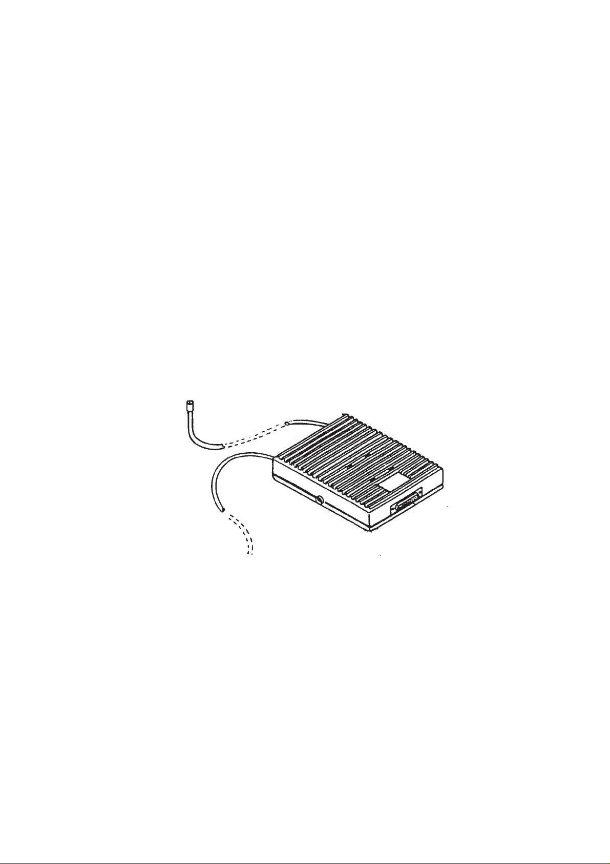
After Sales
Technical Documentation
Figure 4: Exploded View
Booster Kit BSH–1
Assembly Parts
ITEM Q’TY CODE DESCRIPTION VALUE, TYPE
1 9537013 Chassis 1D 21206
2 9537014 Cover 1D 21207
3 2 9780014 Antenna cable 4C 21537
4 24 6150348 Screw FeZn M3x8 DIN7985
5 6500202 Insulating cool pad TO–220
6 6430144 Plastic rivet 4.0x3.0
socket 6.4
7 9510105 RF shield 1 2D 21209
8 9510104 RF shield 2 2D 21208
9 9307501 Antenna label 3N 7940 PA60TG
10 Type label BSH–1
11
C1 0200100 Booster module BB3
Original, 09/94 Page 21
Page 22

Booster Kit BSH–1
After Sales
Technical Documentation
[This page intentionally left blank]
Original, 09/94Page 22
 Loading...