

Page 1
After Sales Technical Documentation
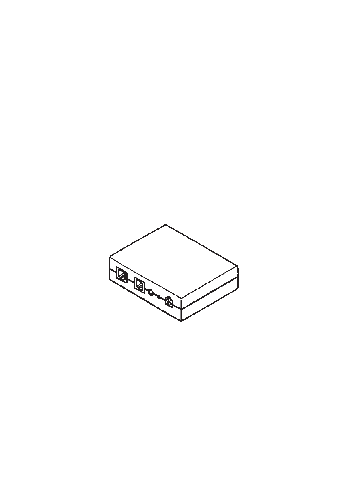
HF JUNCTION BOX
HFJ–2
Original, 05/94 NMP Part No. 0275008
Page 2
HF Junction Box HFJ–2
AMENDMENT RECORD SHEET
After Sales
Technical Documentation
Amendment
Number
Date Inserted By Comments
Page 2
Original, 05/94
Page 3

After Sales
Technical Documentation
HF Junction Box HFJ–2
HF JUNCTION BOX HFJ–2
CONTENTS
Page No
Introduction 5
General 5
Main Features 5
Accessories Supply Voltage 5
Audio Switches 5
Handsfree Audio Amplifiers 5
Charger 5
External I/O 5
Booster Interface 5
Modes of Operation 5
Power–off Mode 5
Power–down Mode 6
Power–on Mode 6
External Signals and Connections 6
Power Supply Connector X210 6
External Microphone X230 6
External Speaker X250 6
Accessory Connector X170 7
Phone Connector X290 7
Functional Description 8
Circuit Description 8
Control Block 8
Booster Interface 8
Charger 9
Audio Switches 10
External I/O 11
Power Supply 11
Microphone Amplifier 12
Speaker Amplifier 12
Parts List 15
Original, 05/94
Page 3
Page 4

HF Junction Box HFJ–2
Technical Documentation
Assembly Parts 22
After Sales
List of Figures
Figure 1: Block Diagram 13
Figure 2: Component Layout Diagram 14
Figure 3: Exploded View 22
Figure 4: Circuit Diagram NO TAG
Page 4
Original, 05/94
Page 5

After Sales
Technical Documentation
Introduction
General
The HFJ–2 Handsfree Junction Box provides and controls the supply voltages for the accessories rge current for the phone. In addition, it controls
the audio paths to the accessories and handsfree equipment.
The unit contains a protection circuit against battery voltage transients,
power switch, handsfree speaker and microphone amplifiers, audio
switches, external I/O, switch mode charger and a microprocessor which
communicates with the phone via the mbus interface.
The BABT approved version of HFJ–2 is known as HFJ–2X. Since both
units are technically identical, all references to HFJ–2 equally apply to
HFJ–2X.
HF Junction Box HFJ–2
Main Features
Accessories Supply Voltage
Filtered and switched voltages are supplied to peripheral devices and to
handsfree audio parts in the HFJ–2 box. Protection against disturbances,
such as overvoltages, transients in incoming battery voltage, is provided.
Audio Switches
Controls audio paths between phone, handsfree equipment and
accessories.
Handsfree Audio Amplifiers
External microphone and speaker amplifiers for handsfree operation.
Charger
Provides supply voltage and charge current for phone.
External I/O
Open collector output, capable of driving an external relay.
Booster Interface
When requested via mbus message, HFJ–2 can read booster tuning values from booster EEPROM and send them to the phone. Tuning values
can also be written to booster EEPROM.
Modes of Operation
Power–off Mode
The battery voltage is always connected to the accessory and charger
power switches. The rest of the circuitry does not receive supply voltages.
Original, 05/94
Page 5
Page 6
HF Junction Box HFJ–2
Power–down Mode
+5 V supply voltages are switched on. The processor is in power down
mode and its clock oscillator is not running.
Power–on Mode
The processor is executing code. +5 V supply voltages are on and other
supply voltages are under processor control.
External Signals and Connections
The module is provided with five external connectors: power supply connector, external microphone connector, external speaker connector, phone
connector, and accessory connector.
Power Supply Connector X210
After Sales
Technical Documentation
Pin Name Description
1 XCRM External car radio mute: open collector output is pulled down-
when radio is muted, when radio is not muted, collector output
is in a high impedance state. The load relay should be connected between this pin (1) and +Vbat.
– on state max. voltage: +1 V
– on state max. current: 250 mA
– off state max. current: 1 mA
– load resistance min.: 64 Ω
2 IGNS Input controlling auto power off function: should be connected
to car ignition switch (after switch) when in use and to ground
when not in use.
3 GND Power supply ground: should be connected to car battery neg-
ative terminal.
4 +VBAT Power supply voltage: should be connected to car battery posi-
tive terminal.
External Microphone X230
Pin Name Description
1 GND Ground for external microphone.
2 HFMIC Supply voltage for microphone / audio signal from microphone.
External Speaker X250
Pin Name Description
1 GND Ground for external speaker.
2 HFSP Audio signal (d.c.) to speaker/speaker indication.
Page 6
Original, 05/94
Page 7
After Sales
Technical Documentation
Accessory Connector X170
Pin Name Description
1 +VBS Power supply for accessories; HFJ–2 turns this voltage on and
off under phone control.
2 DGND Digital Ground.
3 M2BUS Serial mbus data between handset, HFJ–2 and accessories.
4 LSP Not Connected.
5 PWR This signal is pulled to +5 V at HFJ–2 via an internal resistor.
Indicates external handset power–on switch state to HFJ–2.
6 AGND Analog Ground.
7 MIC Audio signal from accessories to phone (transmitted audio) or
HF speaker (voice dialer phrase, answer machine message).
8 EAR Audio signal from phone (received audio) or from HF micro-
phone to accessories.
HF Junction Box HFJ–2
Phone Connector X290
Pin Name Description
1 SCL/TXI IIC bus clock for booster; this signal is pulled to +5 V at HFJ–2
via the internal resistor of the processor. This pin is also used
for booster error indication; in error condition, the booster pulls
this pin (1) down (pin 1 can be used as an output to the boost-
er at the same time). Periodically, Pin 1 is changed to input for
60 s time and TXI state is polled. These polling pulses must
be filtered in the booster.
2 PGND Ground for charger.
3 M2BUS Serial mbus data between phone, HFJ–2 and accessories.
4 VC Supply voltage/charging current for phone.
5 HOOD/SDA Handset hook ind./IIC bus data for booster.
6 SGND Signal ground.
7 XMIC/
JCONN
8 XEAR/
HFJPWR
Audio signal from accessories or HF microphone to phone:
100 kΩ pull–up to +5 V; d.c. level indicates connection of
HFJ–2 box to phone.
Audio signal from phone (received audio) to accessories or HF
speaker: 1 MΩ pull–up resistor to +VBAT, drop down of current
from this pin turns on +5 V supply to the processor.
Original, 05/94
Page 7
Page 8

HF Junction Box HFJ–2
Functional Description
Circuit Description
The BC4 module can be divided into seven blocks as follows:
– control
– charger
– audio switches
– external I/O
– power supply
– microphone amplifier
– speaker amplifier
Control Block
The main parts of the control block are the microcontroller D130
(83C51FA), mbus, and interrupt logic. D130 controls the audio paths, the
charger, external I/O, the booster interface and the accessory power
switch.
After Sales
Technical Documentation
Interrupts are obtained from three sources: car ignition switch, handset’s
power switch, and mbus. Their purpose is to wake up the controller from
power down mode. Mbus is the interface between the phone and other accessories except the booster. There are bidirectional buffer in mbus line,
which regenerates the mbus signal.
Booster Interface
Tuning values from booster EEPROM are read immediately after power on
(phone is connected to holder or wake up from power down). It is possible
to read EEPROM values via mbus request, but it should not be done during conversation.
If booster EEPROM data and checksum are correct, tuning values are
send to the phone and SCL/TXI line polling begins. If low level is detected
phone is informed via mbus message. SCL/TXI line can be used as output
at the same time and controlled by mbus messages. If no message is
sent, the output state goes ”high”. Periodically SCL/TXI is changed to input
and its state is read. This polling causes pulses, whitch must be filtered in
booster.
Signals passed between the control block and the other blocks are shown in the
following table:
Page 8
Original, 05/94
Page 9

After Sales
Technical Documentation
Name Description
PWR_ON Accessory power switch on/off.
CH_ON Charger on/off.
SCL/TXI IIC bus clock for booster/booster error indication.
IO_EN Voltage for several pull–up resistors (see circuit diagram). In power
down mode, this signal is low level, to reduce current consumption.
XPWR Handset’s power on switch state.
IGNS Car ignition switch state.
RXD Mbus receive data.
TXD Mbus transmit data.
CRM Car radio mute
HP_MIC Audio switch control between phone’s xmic and accessories mic
HP_HFM Audio switch control between phone’s xmic and handsfree micro-
phone
HF Junction Box HFJ–2
HF_EAR Audio switch control between accessories ear and handsfree speaker
HF_MIC Audio switch control between accessories mic and handsfree micro-
phone
HP_EAR Audio switch control between phone’s xear and accessories ear
HP_HFS Audio switch control between phone’s xear and handsfree speaker
SIDE_T Sidetone from X170 MIC to EAR control.
CHV Charger voltage control, 12 or 15 V.
LO_V Low voltage indication – generates reset for processor.
Charger
The charger is a switching mode voltage/current source. The switching frequency is fixed at approx. 80 kHz, generated by a separate RC oscillator.
The charger has voltage and current feedback. At a light load (less than
800 mA current), the charger acts as a 12 V (or 15 V) voltage regulator;
with a heavier load, it acts as a 800 mA current regulator. Input voltage
can be higher or lower than the output voltage.
Signals passed between the charger block and the other blocks are shown in the
following table:
Original, 05/94
Page 9
Page 10

HF Junction Box HFJ–2
Name Description
+VPB Supply voltage for power section
+VCH Supply voltage for oscillator and comparators
CH_ON On/off control
LO_V Low voltage turn off
IO_EN Reference voltage +5 V
+VC Output voltage/current
PGND Ground for output (”power ground”)
Audio Switches
Audio paths are controlled by seven CMOS analog switches N320 and
N310. Paths for microphone and ear/speaker signals between phone and
accessories, phone and handsfree, handsfree and accessories are possible. XEAR and XMIC lines from the phone includes a differential buffer
amplifier N230. Both audio paths have d.c. decoupling capacitors, internal
d.c. levels are 2.4 V.
After Sales
Technical Documentation
Signals passed between the audio switch block and the other blocks are shown in
the following table:
Name Description
HP_HFS See description of control block
HP_EAR See description of control block
HF_MIC See description of control block
HF_EAR See description of control block
HP_HFM See description of control block
HP_MIC See description of control block
+2.4V Internal d.c. levels
+5V External d.c. levels
SIDE_T Sidetone on/off
XEAR/
HFPWR
XMIC/
JCONN
MIC Audio signal to/from accessories
Received audio signal from handset
Transmitted audio signal to handset
EAR Audio signal to/from accessories
Page 10
Original, 05/94
Page 11

After Sales
Technical Documentation
External I/O
The external I/O block consists of the car ignition key sense function and
car radio mute function. When pin 2 at connector X210 is connected to the
battery supply voltage, an interrupt pulse for the processor is generated. If
the processor is in power down mode it powers up. The processor can
also read the ignition key state. In the power on mode, this state is continuously polled, and an mbus message is sent to the phone, when this state
changes.
Car radio mute is an open collector output capable of driving a relay. The
purpose of the mute function is to mute the car radio during conversation.
This output has a short circuit protection, which is triggered when pin 1 at
X210 is directly connected to car battery voltage, while the output is turned
on. When triggered, the output switches off and remains off, until it has
been turned off and on again.
HF Junction Box HFJ–2
Signals passed between the ext. i/o block and the other blocks are shown in the
following table:
Name Description
IGNS Car ignition key status to processor and interrupt pulse generator.
CRM CRM on/off control from processor.
X210.2 IGNS input in connector X210.
X210.1 CRM output in connector X210.
Power Supply
The power supply provides a +5 V supply voltage for the processor and a
+VCH voltage for the charger. When the xear/hfpwr line is connected to
ground, via the 100 kΩ resistor, +5V voltage turns on. When +5 V is turned
on, the processor can control +VCH.
When the supply voltage from the car battery is too low or regulator N270
can’t provide a stable +5 V, an error signal is generated by the power supply. This error signal is used to disable the charger and acts as a reset signal for the processor.
Signals passed between the power supply block and the other blocks are shown in
the following table:
Name Description
+VBP Protected car battery voltage, supply voltage for this block.
+VCH Charger supply voltage.
HFPWR Power on/off control.
+5V +5V supply voltage, output of this block.
LO_V Low voltage error indication.
Original, 05/94
Page 11
Page 12

HF Junction Box HFJ–2
Technical Documentation
Microphone Amplifier
The handsfree microphone signal is amplified in N230, and directed to the
handportable XMIC line or the accessories MIC line in the audio switch
block. The accessory supply voltage (+VBS) is the supply voltage for the
Microphone Amplifier also and hence must be available.
Signals passed between the mic. amp. block and other blocks are as shown in the
following table:
Name Description
HF_MIC Amplified handsfree microphone output signal to audio switch block.
+12V Supply voltage.
+2.4V Internal d.c. level reference.
X290.2 Handsfree microphone input.
GAIN Gain selection input, low level at this input gives higher gain.
After Sales
Speaker Amplifier
This is a 4 W power amplifier for the handsfree loudspeaker. Audio signals
from phone XEAR or accessories EAR lines are directed via the audio
switch block to speaker amplifier N250. The gain is constant. The accessory supply voltage (+VBS) is the supply voltage for the Speaker Amplifier
also and hence must be available.
Signals passed between the speaker amplifier block and other blocks are as shown
in the following table:
Name Description
+12V Supply voltage.
+2.4V Internal d.c. level reference.
HF_SP Handsfree speaker input.
X250.2 Handsfree speaker output.
Page 12
Original, 05/94
Page 13

After Sales
Technical Documentation
HF Junction Box HFJ–2
Figure 1: Block Diagram Version 5.0
3A 0694006
Original, 05/94
Page 13
Page 14

HF Junction Box HFJ–2
Figure 2: Component Layout Diagram
After Sales
Technical Documentation
Page 14
Original, 05/94
Page 15

After Sales
Technical Documentation
HF Junction Box HFJ–2
Parts List
ITEM CODE DESCRIPTION VALUE TYPE
R101 1412409 Chip resistor 1.5 k 5 % 0.063 W 0805
R102 1412430 Chip resistor 10 k 5 % 0.063 W 0805
R103 1414212 Chip resistor 330 k 5 % 0.063 W 0805
R104 1412511 Chip resistor 18 k 5 % 0.063 W 0805
R105 1413635 Chip resistor 100 k 5 % 0.063 W 0805
R106 1400844 Melf resistor 0.33 2 % 0.7 W 6.5x2.5
R107 1414406 Chip resistor 5.6 k 5 % 0.063 W 0805
R108 1412430 Chip resistor 10 k 5 % 0.063 W 0805
R109 1413635 Chip resistor 100 k 5 % 0.063 W 0805
R110 1413635 Chip resistor 100 k 5 % 0.063 W 0805
R111 1412430 Chip resistor 10 k 5 % 0.063 W 0805
R112 1414406 Chip resistor 5.6 k 5 % 0.063 W 0805
R113 1414406 Chip resistor 5.6 k 5 % 0.063 W 0805
R114 1413635 Chip resistor 100 k 5 % 0.063 W 0805
R115 1411669 Chip resistor 22 5 % 0.063 W 0805
R116 1412536 Chip resistor 22 k 5 % 0.063 W 0805
R117 1412430 Chip resistor 10 k 5 % 0.063 W 0805
R118 1412416 Chip resistor 2.2 k 5 % 0.063 W 0805
R119 1412430 Chip resistor 10 k 5 % 0.063 W 0805
R132 1413635 Chip resistor 100 k 5 % 0.063 W 0805
R133 1413635 Chip resistor 100 k 5 % 0.063 W 0805
R134 1413804 Chip resistor 1.0 M 5 % 0.063 W 0805
R135 1413635 Chip resistor 100 k 5 % 0.063 W 0805
R136 1413635 Chip resistor 100 k 5 % 0.063 W 0805
R137 1413635 Chip resistor 100 k 5 % 0.063 W 0805
R138 1413635 Chip resistor 100 k 5 % 0.063 W 0805
R139 1413635 Chip resistor 100 k 5 % 0.063 W 0805
R140 1413635 Chip resistor 100 k 5 % 0.063 W 0805
R142 1413635 Chip resistor 100 k 5 % 0.063 W 0805
R145 1412409 Chip resistor 1.5 k 5 % 0.063 W 0805
R146 1413804 Chip resistor 1.0 M 5 % 0.063 W 0805
R147 1413635 Chip resistor 100 k 5 % 0.063 W 0805
R148 1412409 Chip resistor 1.5 k 5 % 0.063 W 0805
R149 1413635 Chip resistor 100 k 5 % 0.063 W 0805
R151 1412409 Chip resistor 1.5 k 5 % 0.063 W 0805
R152 1413635 Chip resistor 100 k 5 % 0.063 W 0805
R153 1413635 Chip resistor 100 k 5 % 0.063 W 0805
R154 1413635 Chip resistor 100 k 5 % 0.063 W 0805
R155 1413635 Chip resistor 100 k 5 % 0.063 W 0805
Original, 05/94
Page 15
Page 16

HF Junction Box HFJ–2
Technical Documentation
R156 1413635 Chip resistor 100 k 5 % 0.063 W 0805
R157 1413635 Chip resistor 100 k 5 % 0.063 W 0805
R158 1413804 Chip resistor 1.0 M 5 % 0.063 W 0805
R159 1412729 Chip resistor 33 k 5 % 0.063 W 0805
R160 1413829 Chip resistor 10 5 % 0.063 W 0805
R170 1412261 Chip resistor 100 5 % 0.063 W 0805
R171 1412261 Chip resistor 100 5 % 0.063 W 0805
R172 1412430 Chip resistor 10 k 5 % 0.063 W 0805
R173 1413635 Chip resistor 100 k 5 % 0.063 W 0805
R174 1412303 Chip resistor 330 5 % 0.063 W 0805
R190 1412430 Chip resistor 10 k 5 % 0.063 W 0805
R191 1412430 Chip resistor 10 k 5 % 0.063 W 0805
R192 1412416 Chip resistor 2.2 k 5 % 0.063 W 0805
R193 1412430 Chip resistor 10 k 5 % 0.063 W 0805
R194 1413804 Chip resistor 1.0 M 5 % 0.063 W 0805
R195 1413635 Chip resistor 100 k 5 % 0.063 W 0805
R211 1413716 Chip resistor 220 k 5 % 0.063 W 0805
R212 1412409 Chip resistor 1.5 k 5 % 0.063 W 0805
R213 1413635 Chip resistor 100 k 5 % 0.063 W 0805
R214 1413635 Chip resistor 100 k 5 % 0.063 W 0805
R215 1413635 Chip resistor 100 k 5 % 0.063 W 0805
R216 1413635 Chip resistor 100 k 5 % 0.063 W 0805
R217 1412409 Chip resistor 1.5 k 5 % 0.063 W 0805
R219 1412729 Chip resistor 33 k 5 % 0.063 W 0805
R230 1414212 Chip resistor 330 k 5 % 0.063 W 0805
R235 1412416 Chip resistor 2.2 k 5 % 0.063 W 0805
R236 1412416 Chip resistor 2.2 k 5 % 0.063 W 0805
R237 1412416 Chip resistor 2.2 k 5 % 0.063 W 0805
R250 1412409 Chip resistor 1.5 k 5 % 0.063 W 0805
R251 1413829 Chip resistor 10 5 % 0.063 W 0805
R252 1412729 Chip resistor 33 k 5 % 0.063 W 0805
R253 1412536 Chip resistor 22 k 5 % 0.063 W 0805
R254 1413829 Chip resistor 10 5 % 0.063 W 0805
R255 1412536 Chip resistor 22 k 5 % 0.063 W 0805
R256 1412303 Chip resistor 330 5 % 0.063 W 0805
R270 1414212 Chip resistor 330 k 5 % 0.063 W 0805
R271 1413804 Chip resistor 1.0 M 5 % 0.063 W 0805
R272 1414406 Chip resistor 5.6 k 5 % 0.063 W 0805
R273 1412409 Chip resistor 1.5 k 5 % 0.063 W 0805
R290 1412409 Chip resistor 1.5 k 5 % 0.063 W 0805
R291 1412409 Chip resistor 1.5 k 5 % 0.063 W 0805
R292 1412303 Chip resistor 330 5 % 0.063 W 0805
After Sales
Page 16
Original, 05/94
Page 17

After Sales
Technical Documentation
R293 1412303 Chip resistor 330 5 % 0.063 W 0805
R294 1412303 Chip resistor 330 5 % 0.063 W 0805
R295 1412430 Chip resistor 10 k 5 % 0.063 W 0805
R296 1412261 Chip resistor 100 5 % 0.063 W 0805
R299 1413716 Chip resistor 220 k 5 % 0.063 W 0805
R310 1416160 Melf resistor 100 k 1 % 0.2 W 0204
R311 1416160 Melf resistor 100 k 1 % 0.2 W 0204
R312 1412409 Chip resistor 1.5 k 5 % 0.063 W 0805
R313 1412409 Chip resistor 1.5 k 5 % 0.063 W 0805
R314 1414212 Chip resistor 330 k 5 % 0.063 W 0805
R315 1416160 Melf resistor 100 k 1 % 0.2 W 0204
R316 1416160 Melf resistor 100 k 1 % 0.2 W 0204
R317 1416160 Melf resistor 100 k 1 % 0.2 W 0204
R318 1413635 Chip resistor 100 k 5 % 0.063 W 0805
R319 1413635 Chip resistor 100 k 5 % 0.063 W 0805
R320 1412416 Chip resistor 2.2 k 5 % 0.063 W 0805
R321 1416160 Melf resistor 100 k 1 % 0.2 W 0204
R322 1412416 Chip resistor 2.2 k 5 % 0.063 W 0805
R324 1413642 Chip resistor 56 k 5 % 0.063 W 0805
R325 1413642 Chip resistor 56 k 5 % 0.063 W 0805
R326 1412430 Chip resistor 10 k 5 % 0.063 W 0805
R327 1412430 Chip resistor 10 k 5 % 0.063 W 0805
R328 1412416 Chip resistor 2.2 k 5 % 0.063 W 0805
R340 1412416 Chip resistor 2.2 k 5 % 0.063 W 0805
R341 1414406 Chip resistor 5.6 k 5 % 0.063 W 0805
R342 1412430 Chip resistor 10 k 5 % 0.063 W 0805
R343 1412729 Chip resistor 33 k 5 % 0.063 W 0805
R344 1412536 Chip resistor 22 k 5 % 0.063 W 0805
R345 1414406 Chip resistor 5.6 k 5 % 0.063 W 0805
R346 1412416 Chip resistor 2.2 k 5 % 0.063 W 0805
R347 1413716 Chip resistor 220 k 5 % 0.063 W 0805
R348 1413723 Chip resistor 470 k 5 % 0.063 W 0805
R349 1412536 Chip resistor 22 k 5 % 0.063 W 0805
R350 1412729 Chip resistor 33 k 5 % 0.063 W 0805
R351 1412430 Chip resistor 10 k 5 % 0.063 W 0805
R352 1412416 Chip resistor 2.2 k 5 % 0.063 W 0805
R353 1414406 Chip resistor 5.6 k 5 % 0.063 W 0805
C100 2310791 Ceramic cap. 33 n 20 % 50 V 0805
C101 2505261 Electrol. cap. 220 20 % 25 V 8.5x11.5
C102 2404094 Polyester cap. 470 n 10 % 63 V RM5
C103 2404094 Polyester cap. 470 n 10 % 63 V RM5
C104 2310791 Ceramic cap. 33 n 20 % 50 V 0805
HF Junction Box HFJ–2
Original, 05/94
Page 17
Page 18

HF Junction Box HFJ–2
Technical Documentation
C105 2310791 Ceramic cap. 33 n 20 % 50 V 0805
C106 2310738 Ceramic cap. 4.7 n 20 % 50 V 0805
C107 2310488 Ceramic cap. 330 p 5 % 50 V 0805
C109 2310791 Ceramic cap. 33 n 20 % 50 V 0805
C110 2310488 Ceramic cap. 330 p 5 % 50 V 0805
C111 2310791 Ceramic cap. 33 n 20 % 50 V 0805
C130 2310791 Ceramic cap. 33 n 20 % 50 V 0805
C131 2310791 Ceramic cap. 33 n 20 % 50 V 0805
C132 2310791 Ceramic cap. 33 n 20 % 50 V 0805
C133 2310791 Ceramic cap. 33 n 20 % 50 V 0805
C134 2310791 Ceramic cap. 33 n 20 % 50 V 0805
C135 2310343 Ceramic cap. 22 p 5 % 50 V 0805
C136 2310343 Ceramic cap. 22 p 5 % 50 V 0805
C137 2310488 Ceramic cap. 330 p 5 % 50 V 0805
C138 2310488 Ceramic cap. 330 p 5 % 50 V 0805
C139 2604209 Tantalum cap. 1.0 20 % 16 V 3.2x1.6x1.8
C140 2310791 Ceramic cap. 33 n 20 % 50 V 0805
C143 2310791 Ceramic cap. 33 n 20 % 50 V 0805
C144 2310791 Ceramic cap. 33 n 20 % 50 V 0805
C170 2310738 Ceramic cap. 4.7 n 20 % 50 V 0805
C171 2310738 Ceramic cap. 4.7 n 20 % 50 V 0805
C172 2604209 Tantalum cap. 1.0 20 % 16 V 3.2x1.6x1.8
C173 2604209 Tantalum cap. 1.0 20 % 16 V 3.2x1.6x1.8
C174 2310791 Ceramic cap. 33 n 20 % 50 V 0805
C175 2310791 Ceramic cap. 33 n 20 % 50 V 0805
C177 2310488 Ceramic cap. 330 p 5 % 50 V 0805
C190 2604209 Tantalum cap. 1.0 20 % 16 V 3.2x1.6x1.8
C191 2310791 Ceramic cap. 33 n 20 % 50 V 0805
C213 2501605 Electrol. cap. 100 20 % 35 V RM3.5
C214 2310791 Ceramic cap. 33 n 20 % 50 V 0805
C215 2604209 Tantalum cap. 1.0 20 % 16 V 3.2x1.6x1.8
C216 2507479 Electrol. cap. 1000 20 % 25 V 13x20mm
C217 2310791 Ceramic cap. 33 n 20 % 50 V 0805
C230 2310463 Ceramic cap. 220 p 5 % 50 V 0805
C231 2604022 Tantalum cap. 0.1 20 % 35 V 3.2x1.6x1.8
C232 2310791 Ceramic cap. 33 n 20 % 50 V 0805
C250 2310791 Ceramic cap. 33 n 20 % 50 V 0805
C251 2604431 Tantalum cap. 10 20 % 16 V 6.0x3.2x2.8
C252 2604209 Tantalum cap. 1.0 20 % 16 V 3.2x1.6x1.8
C253 2604431 Tantalum cap. 10 20 % 16 V 6.0x3.2x2.8
C254 2404094 Polyester cap. 470 n 10 % 63 V RM5
C256 2505261 Electrol. cap. 220 20 % 25 V 8.5x11.5
After Sales
Page 18
Original, 05/94
Page 19

After Sales
Technical Documentation
C257 2310752 Ceramic cap. 10 n 20 % 50 V 0805
C258 2310791 Ceramic cap. 33 n 20 % 50 V 0805
C270 2604209 Tantalum cap. 1.0 20 % 16 V 3.2x1.6x1.8
C271 2604209 Tantalum cap. 1.0 20 % 16 V 3.2x1.6x1.8
C272 2604209 Tantalum cap. 1.0 20 % 16 V 3.2x1.6x1.8
C273 2604431 Tantalum cap. 10 20 % 16 V 6.0x3.2x2.8
C291 2310791 Ceramic cap. 33 n 20 % 50 V 0805
C293 2310791 Ceramic cap. 33 n 20 % 50 V 0805
C294 2310488 Ceramic cap. 330 p 5 % 50 V 0805
C295 2310488 Ceramic cap. 330 p 5 % 50 V 0805
C296 2310791 Ceramic cap. 33 n 20 % 50 V 0805
C297 2310488 Ceramic cap. 330 p 5 % 50 V 0805
C298 2310488 Ceramic cap. 330 p 5 % 50 V 0805
C310 2310791 Ceramic cap. 33 n 20 % 50 V 0805
C311 2604209 Tantalum cap. 1.0 20 % 16 V 3.2x1.6x1.8
C313 2310738 Ceramic cap. 4.7 n 20 % 50 V 0805
C340 2310424 Ceramic cap. 100 p 5 % 50 V 0805
C341 2310424 Ceramic cap. 100 p 5 % 50 V 0805
C342 2310791 Ceramic cap. 33 n 20 % 50 V 0805
L100 3606698 Choke 60 20 % 1 A FJ1445
L101 3607555 Coil 125 2 A
L102 3607555 Coil 125 2 A
L103 3606698 Choke 60 20 % 1 A FJ1445
L210 3607898 Choke 2 A 900UH/1 kHz DH–TS582
B130 4501008 Crystal 7.3728 M 16PF, 50PPM
V100 4100221 Schottky diode 21DQ06 60 V 1.7 A d3.7x7mm
V101 4200868 MosFet IRF530 n–ch 10 V 14 A TO220
V102 4200917 TransistorBC848B/BCW32 npn 30 V 100 mA SOT23
V103 4200909 TransistorBC858B/BCW30 pnp 30 V 100 mA SOT23
V104 4107160 Zener diode BZX84 5 % 12 V 0.3 W SOT23
V105 4108639 Diode x 2 BAS28 75 V 250 mA SOT143
V106 4200909 TransistorBC858B/BCW30 pnp 30 V 100 mA SOT23
V107 4200917 TransistorBC848B/BCW32 npn 30 V 100 mA SOT23
V108 4200917 TransistorBC848B/BCW32 npn 30 V 100 mA SOT23
V131 4108639 Diode x 2 BAS28 75 V 250 mA SOT143
V132 4106769 Zener diode BZX84 5 % 4.7 V 0.3 W SOT23
V133 4200917 TransistorBC848B/BCW32 npn 30 V 100 mA SOT23
V134 4106769 Zener diode BZX84 5 % 4.7 V 0.3 W SOT23
V190 4200836 Transistor BCX19 npn 50 V 0.5 A SOT23
V191 4108639 Diode x 2 BAS28 75 V 250 mA SOT143
V192 4200917 TransistorBC848B/BCW32 npn 30 V 100 mA SOT23
V193 4200917 TransistorBC848B/BCW32 npn 30 V 100 mA SOT23
HF Junction Box HFJ–2
Original, 05/94
Page 19
Page 20

HF Junction Box HFJ–2
Technical Documentation
V194 4101653 Diode BYD17D 200 V 1.5 A SOD87
V195 4101653 Diode BYD17D 200 V 1.5 A SOD87
V212 4100218 Trans. supr. LDP24A 100 V 30A/40 ms AG
V213 4200603 Transistor BCX17 pnp 45 V 500 mA SOT23
V214 4200603 Transistor BCX17 pnp 45 V 500 mA SOT23
V215 4110195 Zener diode BZX84 5 % 18 V 0.3 W SOT23
V216 4200603 Transistor BCX17 pnp 45 V 500 mA SOT23
V217 4108639 Diode x 2 BAS28 75 V 250 mA SOT143
V218 4209990 MosFet IRF9530 p–ch 10 V 12 A TO220
V219 4200836 Transistor BCX19 npn 50 V 0.5 A SOT23
V230 4110117 Zener diode BZX84 5 % 3.9 V 0.3 W SOT23
V270 4200836 Transistor BCX19 npn 50 V 0.5 A SOT23
V271 4108639 Diode x 2 BAS28 75 V 250 mA SOT143
V272 4110195 Zener diode BZX84 5 % 18 V 0.3 W SOT23
V273 4116536 Zener diode BZX84 5 % 2.4 V 0.3 W SOT23
V274 4200603 Transistor BCX17 pnp 45 V 500 mA SOT23
V290 4106769 Zener diode BZX84 5 % 4.7 V 0.3 W SOT23
V291 4106769 Zener diode BZX84 5 % 4.7 V 0.3 W SOT23
V292 4107160 Zener diode BZX84 5 % 12 V 0.3 W SOT23
V293 4106769 Zener diode BZX84 5 % 4.7 V 0.3 W SOT23
V311 4106769 Zener diode BZX84 5 % 4.7 V 0.3 W SOT23
V312 4106769 Zener diode BZX84 5 % 4.7 V 0.3 W SOT23
V340 4200917 TransistorBC848B/BCW32 npn 30 V 100 mA SOT23
V341 4200917 TransistorBC848B/BCW32 npn 30 V 100 mA SOT23
V342 4200909 TransistorBC858B/BCW30 pnp 30 V 100 mA SOT23
V343 4108639 Diode x 2 BAS28 75 V 250 mA SOT143
V344 4200909 TransistorBC858B/BCW30 pnp 30 V 100 mA SOT23
V345 4200917 TransistorBC848B/BCW32 npn 30 V 100 mA SOT23
V346 4200917 TransistorBC848B/BCW32 npn 30 V 100 mA SOT23
V347 4107160 Zener diode BZX84 5 % 12 V 0.3 W SOT23
D130 4375034 IC, MCU PLCC44
D131 4309914 IC, 6 x sch.inv 74HC14 SO14
N100 4305236 IC, 2 x comp. LM2903 SO8S
N110 4301199 IC, 2 x op.amp. LM2904 SO8S
N230 4301182 IC, 2 x op.amp. LM2902 SO14S
N250 4303439 IC, af amp4w/14v 4–20v dil1 TDA1904 DIL16S
N270 4301062 IC, regulator LP2951AC SO8S
N310 4309488 IC, 4 x bi.switch 74HC4066 SO14S
N320 4309488 IC, 4 x bi.switch 74HC4066 SO14S
X170 5416517 Modular jack 8 pin pcb
X210 5439668 Connector 2x2 pole right angle PCB
X230 5407002 Jack 2,5mm horizontal female pcb
After Sales
Page 20
Original, 05/94
Page 21

After Sales
Technical Documentation
X250 5407006 Jack 3,5mm horizontal female pcb
X290 5416517 Modular jack 8 pin pcb
4340082 IC, MCU PLCC44
9380149 Sticker brady lat–2–747 9.5x9.5
3200047 Ferrite ring d 3.5x1.3x4.3mm f2
7510302 Adhesive stick jet–melt tc–3748
9510077 Emc–chassis1 3D21557 THX–7X,THN–thx–7x,thn–7
9730043 Ns–strip 0.4x128 cuni12zn24–04
9853848 PC board BC4A 114.9x79.5x1.6 d 2/pa
0240120 IC, SWRAM SW HFJ–2/3
HF Junction Box HFJ–2
Original, 05/94
Page 21
Page 22

HF Junction Box HFJ–2
Figure 3: Exploded View
After Sales
Technical Documentation
Assembly Parts
ITEM Q’TY CODE DESCRIPTION VALUE, TYPE
1 9450050 Cover 1D 21289
1 9450067 Cover 1D 21307
2 9510078 EMC cover 3D 21558
3 9450066 Bottom cover 1D 21305
4 4 6292014 PT screw KB25x16 WN1442 FeZn
5 9370113 Type label 4D 21617
C1 0200045 BC4 charging module
Page 22
Original, 05/94
 Loading...