

Page 1
After Sales Technical Documentation
COMPACT HANDSFREE
UNIT
PHF–2
Original, 11/94
NMP Part No. 0275013
Page 2

Compact Handsfree Unit PHF–2
AMENDMENT RECORD SHEET
After Sales
Technical Documentation
Amendment
Number
Date Inserted By Comments
Page 2 Original, 11/94
Page 3

After Sales
Technical Documentation
Compact Handsfree Unit PHF–2
COMPACT HANDSFREE UNIT PHF–2
CONTENTS
Page No
Introduction 5
Technical Summary 5
List of Modules 5
Technical Specifications 6
Modes of Operation 6
Maximum Ratings 7
DC Characteristics 7
Control Signals 8
AC Characteristics 8
External Signals and Connections 9
Mechanical Characteristics 9
Functional Description 10
Circuit Description 10
Input Circuit 10
Power Control Logic 12
Switched Mode Power Supply 12
Audio Circuit 12
Assembly 14
Assembly Parts 15
Parts List 15
List of Figures
Figure 1 Block Diagram 10
Figure 2 Component Layout Diagram 11
Figure 3 Cable Interconnection Diagram 13
Figure 4 Exploded View 14
Figure 5 Circuit Diagram 19
Page 3Original, 11/94
Page 4

Compact Handsfree Unit PHF–2
After Sales
Technical Documentation
[This page intentionally left blank]
Page 4 Original, 11/94
Page 5

After Sales
Technical Documentation
Introduction
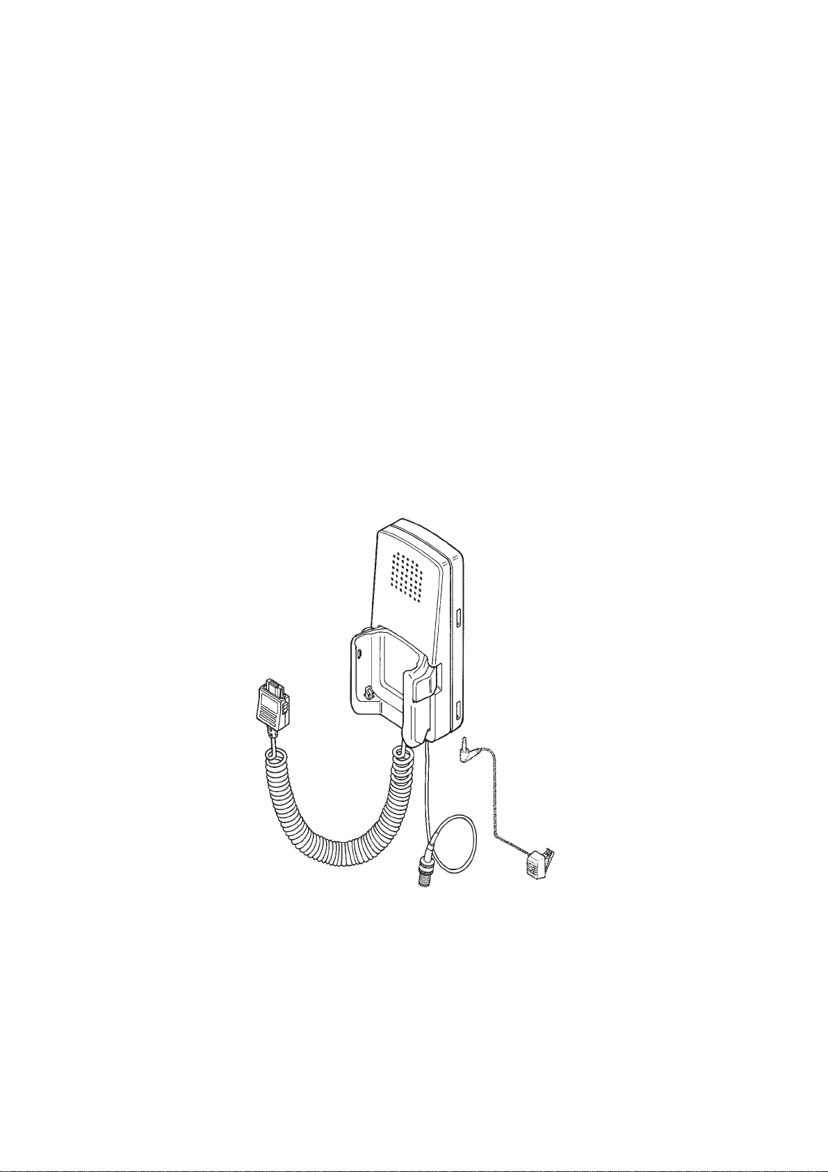
The PHF–2 Compact Handsfree Unit forms a major part of the Compact
Handsfree Car Kit; the kit provides a simple–to–install, low cost handsfree
facility for in–car use.
The BABT approved version of PHF–2 is known as PHF–2X. Since both
units are technically identical, all references to PHF–2 equally apply to
PHF–2X.
Technical Summary
PHF–2 allows both handsfree (hf) and normal handset (hs) use of the
phone. Handset use is possible with the curly system cable which
includes an antenna cable. Detection of hf and hs operation is achieved
by a reed–switch located in the PHF–2 plug which detects the presence of
a magnet inside the MBH–9 holder.
Compact Handsfree Unit PHF–2
The phone is connected to the unit via a system connector (fitted to the
end of the curly system cable). There are also connectors for an external
power source, for a standard hf–microphone and for an external antenna
which must be used with this configuration.
The Compact Handsfree Unit consists of speaker and microphone
amplifiers, power on/off –logic, hf–speaker muting and a constant current
switching regulator for charging the phone battery. The unit has an inbuilt
hf–speaker and an external hf–microphone but the actual handsfree
function is generated in the phone.
MPHF2 mechanics comprise the front and rear covers, speaker
The
clamp, the holder cover, screws, type label, and system cable with
rf–cable.
PHF–2 is installed inside the vehicle using a separate mounting plate
(MKE–1). Depending upon the version of car kit being installed, the
PHF–2 unit is supplied with/without the MBH–9 holder already fitted to the
front of the PHF–2 unit.
List of Modules
Table 1. List of Modules
NAME OF MODULE TYPE
CODE
HF Speaker Module DH3N 0200599
Assembly Parts
PHF–2
Installation Kit PHF–1/M 0260254
MPHF2 0260340
MATERIAL
CODE
NOTES
Page 5Original, 11/94
Page 6
Compact Handsfree Unit PHF–2
After Sales
Technical Documentation
Technical Specifications
Modes of Operation
Power Off : The DH3–module does not receive a supply volt-
age at the DC–connector (X100), hence no
voltages are present on the module.
Standby : The module receives a supply voltage at the DC–
connector but the M2BUS–line (X400) is low (logic
”0” state) because the phone is off and the battery
is fully charged. The switching regulator is off and
there is no supply voltage for the audio.
Power On / Speaker Off : The M2BUS–line is high (logic ”1” state) so the
switching regulator supplies charging current to the
phone. The supply voltage for the audio is on but
the PHFS–line (X400) is low (”0” state) so the HF–
speaker is muted.
Power On / Speaker On : The switching regulator supplies a charging
current to the phone. The supply voltage for the
audio is on and the PHFS–line is high (logic ”1”
state) so the HF–speaker is on.
Table 2. List of Connectors
CONNECTOR NAME CODE NOTES POLES
DC–Supply Connector X100 Power Supply Input Vdc 2–pole
HF–Microphone Connector X200 Microphone Input HFMIC 2–pole
HF–Speaker Connector X300 Speaker Output HFSP 2–pole
System Connector X400 Phone Cable Connector HHP 8–pole
Page 6 Original, 11/94
Page 7

After Sales
Technical Documentation
Maximum Ratings
Compact Handsfree Unit PHF–2
PIN/
CONNECTOR
X100/1 VB 32 Vdc (without damage)
X100/1 VB 1.3 Adc
PIN/
CONNECTOR
X300/1 HFSP 3.5 Vrms
X300/1 HFSP 3.0 W
PIN/
CONNECTOR
X400/1 VC 13 Vdc
X400/1 VC 870 mAdc
X400/1 VC 150 mVp–p ripple 100...500kHz
LINE SYMBOL MAXIMUM UNIT/NOTES
LINE SYMBOL MAXIMUM UNIT/NOTES
LINE SYMBOL MAXIMUM UNIT/NOTES
DC Characteristics
Table 3. Supply Voltage and Power Consumption
PIN/
CONNECTOR
X100/1 VB 10.8 13.2 15.6 Vdc
X100/1 VB 500 600 1200 mAdc
PIN/
CONNECTOR
X400/1 VC 11 12.2 13 Vdc
X400/1 VC 730 800 870 mAdc
LINE SYMBOL MINIMUM TYPICAL/
NOMINAL
Table 4. Charging Current Output
LINE SYMBOL MINIMUM TYPICAL/
NOMINAL
MAXIMUM UNIT/NOTES
MAXIMUM UNIT/NOTES
Page 7Original, 11/94
Page 8

Compact Handsfree Unit PHF–2
Control Signals
Table 5. Control Signals (DC–values)
After Sales
Technical Documentation
PIN/
CONNECTOR
X400/2 M2BUS 0 5 Vdc
X400/3 PHFS 3.6
X400/4 GND (logic) 0 Vdc
X400/5 AGND (audio) 0 Vdc
X400/6 XEAR/HFJPWR 1 2.5 4 Vdc
X400/7 XMIC/JCONN 0 10 Audio–Vdc
X400/8 AGND (audio) 0 Vdc
LINE SYMBOL MINIMUM TYPICAL/
NOMINAL
0
MAXIMUM UNIT/NOTES
5.2
0.7
Vdc (speaker on)
Vdc (speaker off)
AC Characteristics
Table 6. Audio Levels
LINE SYMBOL TYPICAL/NOMINAL UNIT/NOTES
XMIC Cable level 200 mV rms
XEAR Cable level 130 mV rms
Table 7. Audio Gains
LINE SYMBOL TYPICAL/NOMINAL UNIT/NOTES
HF–microphone amplifier gain 40 dB
HF–speaker amplifier gain 27 dB
Table 8. Audio Specifications
ITEM MINIMUM TYPICAL/
NOMINAL
HF–Speaker: SPL 78 80 82 dB/1W/1m
Speaker output power 3.0 W
XEAR input impedance 10 kohm at 1kHz
XMIC output impedance 2.0 kohm at 1kHz
MAXIMUM UNIT/NOTES
Page 8 Original, 11/94
Page 9

After Sales
Technical Documentation
External Signals and Connections
Table 9. DC Supply Connector, Uin 13.2VDC
Compact Handsfree Unit PHF–2
PIN LINE
SYMBOL
1 VB Input Current 0.8 1 mA Power Off
1 VB Input Current 50 70 90 mA Power On, No
1 VB Input Current 0.6 0.8 A Power On,
2 GND Logic Ground
PIN LINE/
SYMBOL
2 HFMIC Output Voltage 5.0 5.8 V
2 HFMIC Internal Resistance 2200 ohms
2 HFMIC Input impedance 1000 ohms
1 GND
PARAMETER MIN TYPICAL/
NOMINAL
Table 10. DC HF–microphone Connector
PARAMETER MIN TYPICAL/
NOMINAL
MAX UNIT/NOTES
Charging
Charging On
MAX UNIT/NOTES
Table 11. DC HF–speaker Connector
PIN LINE/
SYMBOL
1 HFSP Load Impedance 4 ohms
1 HFSP Output Power 3 W
2 GND
PARAMETER MIN TYPICAL/
NOMINAL
MAX UNIT/NOTES
Mechanical Characteristics
Table 12. Mechanical Characteristics
UNIT DIMENSIONS (mm)
(W x H x D)
PHF–2 68 x 160 x 34.5 320 0.18 (coiled)
WEIGHT
(g)
CABLE
LENGTH
(m)
1.8 (uncoiled)
ENCLOSURE
(MATERIAL
ETC.),
COLOUR
Material:
G Cycloy ,
C1000 HF
Colour: Warm
Black
Page 9Original, 11/94
Page 10

Compact Handsfree Unit PHF–2
Functional Description
Figure 1: Block Diagram
POWER SUPPLY
After Sales
Technical Documentation
AUDIO REGULATOR
THERMAL
PROTECTION
Circuit Description
Input Circuit
The input circuit contains the following components:
– C1 – EMI capacitor
HANDSFREE
MICROPHONE
AMPLIFIER
SWITCHED MODE
POWER SUPPLY
HANDSFREE
LOUDSPEAKER
AMPLIFIER
– F1 – foil fuse
– L1 / L2 – EMI suppressor chokes
– V1 – voltage suppressor diode (zener type)
Page 10 Original, 11/94
Page 11

After Sales
Technical Documentation
Figure 2: Component Layout Diagram
Compact Handsfree Unit PHF–2
Page 11Original, 11/94
Page 12

Compact Handsfree Unit PHF–2
Power Control Logic
Power is applied to the audio devices via P–FET V410 and 10V regulator
N100 (VBSW) when the M2BUS signal goes high. The XEAR signal can
also switch the power on for 5 seconds as the XEAR signal goes low. The
same 5 second power–on also occurs when power is applied and the
MBUS and XEAR signals are low. C11 acts as a timing capacitor to
generate this second period.
Switched Mode Power Supply
The VBSW voltage generated by N100 powers reference regulator N402
which starts the switched mode power supply (SMPS). V409 provides the
initial current to a totally empty battery. V410 is a constant current source
which sets the voltage level of R408 – the same voltage occurs across the
current shunt resistor R410 when the SMPS is operating. N401a acts like
a pulse width modulator; N401b in conjunction with R407, C408 and V408
generates a minimum pulse width for the SMPS. R405 and R406 disable
the pulse width modulator (N401a), turning off the SMPS when the VB
input voltage is greater than 17V. V407 limits the comparator power
supply VCC; V408 and V406 limit the output voltage of the comparator.
V403 and C403 form a ’bootstrap’ circuit which acts like a voltage doubler
to supply power to the V400 power switch. L401 (L402), R403 and C405
are EMI suppression components. L400 forms the main SMPS inductor;
V411 limits the maximum output voltage.
After Sales
Technical Documentation
Audio Circuit
The N200c, R201 and R202 combination generates a +5VA audio dc
voltage. V202 is the microphone voltage regulator; N200b is the
microphone amplifier; N200a is a differential amplifier which eliminates
disturbances generated in the curly cable ground wire. N200d has the
same function in the XEAR–line. R235 and C231 form a low pass filter
designed to eliminate high frequency noise. N300 is the power amplifier
which supplies the signal to drive the loudspeaker. Components R301,
R302 and C303 serve to stabilize the operation of the power amplifier at
high frequencies.
Page 12 Original, 11/94
Page 13

After Sales
Technical Documentation
Figure 3: Cable Interconnection Diagram
Compact Handsfree Unit PHF–2
Mini UHF
Connector
PHF–2
CONNECTOR
(TO X400)
X002_1 VC
X002_3 XEXAUD
/PHFS
X002_8 AGND
X002_6 XEAR
X002_4 DGND
X002_2 MBUS
X002_5 AGND
X002_7 XMIC
W001
WHITE
GREEN
BLUE
YELLOW
BROWN
RED
BLACK
ORANGE
E1
E2
E4
E6
E7
E3
E8
E5
S1
C1
68n
Mini RF
Connector
X001
PHONE
CONNECTOR
X1–1 VC
X1–2 XEXAUD
/PHFS
X1–3 HOOK
X1–4 XEAR
X1–5 DGND
X1–6 VC
X1–7 MBUS
X1–8 AGND
X1–9 XMIC
W001 CORD
(9780098)
X1–10 DGND
PCB
DC7 MODULE
(0200376)
Page 13Original, 11/94
Page 14

Compact Handsfree Unit PHF–2
Assembly
Figure 4: Exploded View
After Sales
Technical Documentation
Page 14 Original, 11/94
Page 15

After Sales
Technical Documentation
Compact Handsfree Unit PHF–2
Assembly Parts
ITEM QTY CODE DESCRIPTION VALUE
1 1 9450368 Front Cover D6472
2 1 9450255 Cover B 1D22197
3 1 9450369 Cover C D6473
4 1 9380154 Type Label 4D22419
5 2 6293012 Pt–Screw KB22X8 WN1442
6 1 5140098 Loudspeaker 4C23574
7 1 0200376 DC7 Connector Module
8 1 9510211 Holder 4D24728
9 1 9309555 Loudspeaker Cloth A4D40368
10 1 5469800 Accessory Plug Casing MQ138–NKK
11 4 6292240 Pt–Screw KB25X14 WN1441
12 1 9380378 Silver Label (Blank) 4D24
13 1 9380488 BABT Label (PHF–2X only) A12455
Parts List
ITEM CODE DESCRIPTION VALUE TYPE
R011 1413635 Chip resistor 100 k 5 % 0.063 W 0805
R012 1412536 Chip resistor 22 k 5 % 0.063 W 0805
R013 1413635 Chip resistor 100 k 5 % 0.063 W 0805
R015 1412430 Chip resistor 10 k 5 % 0.063 W 0805
R021 1413635 Chip resistor 100 k 5 % 0.063 W 0805
R022 1413635 Chip resistor 100 k 5 % 0.063 W 0805
R031 1413635 Chip resistor 100 k 5 % 0.063 W 0805
R032 1412430 Chip resistor 10 k 5 % 0.063 W 0805
R041 1413635 Chip resistor 100 k 5 % 0.063 W 0805
R201 1413635 Chip resistor 100 k 5 % 0.063 W 0805
R202 1413635 Chip resistor 100 k 5 % 0.063 W 0805
R211 1412261 Chip resistor 100 5 % 0.063 W 0805
R212 1413635 Chip resistor 100 k 5 % 0.063 W 0805
R213 1412416 Chip resistor 2.2 k 5 % 0.063 W 0805
R214 1414029 Chip resistor 3.3 k 5 % 0.063 W 0805
R215 1414131 Chip resistor 180 k 5 % 0.063 W 0805
R216 1414212 Chip resistor 330 k 5 % 0.063 W 0805
R217 1414283 Chip resistor 100 k 1 % 0.063 W 0805
R220 1414283 Chip resistor 100 k 1 % 0.063 W 0805
R221 1412430 Chip resistor 10 k 5 % 0.063 W 0805
Page 15Original, 11/94
Page 16

Compact Handsfree Unit PHF–2
Technical Documentation
R222 1412335 Chip resistor 1.0 k 5 % 0.063 W 0805
R223 1412430 Chip resistor 10 k 5 % 0.063 W 0805
R224 1412430 Chip resistor 10 k 5 % 0.063 W 0805
R225 1412430 Chip resistor 10 k 5 % 0.063 W 0805
R226 1414283 Chip resistor 100 k 1 % 0.063 W 0805
R227 1414283 Chip resistor 100 k 1 % 0.063 W 0805
R231 1414283 Chip resistor 100 k 1 % 0.063 W 0805
R232 1414283 Chip resistor 100 k 1 % 0.063 W 0805
R233 1414283 Chip resistor 100 k 1 % 0.063 W 0805
R234 1414283 Chip resistor 100 k 1 % 0.063 W 0805
R235 1414109 Chip resistor 15 k 5 % 0.063 W 0805
R236 1412430 Chip resistor 10 k 5 % 0.063 W 0805
R301 1413829 Chip resistor 10 5 % 0.063 W 0805
R302 1413829 Chip resistor 10 5 % 0.063 W 0805
R303 1412261 Chip resistor 100 5 % 0.063 W 0805
R304 1412416 Chip resistor 2.2 k 5 % 0.063 W 0805
R305 1412261 Chip resistor 100 5 % 0.063 W 0805
R308 1414109 Chip resistor 15 k 5 % 0.063 W 0805
R309 1412430 Chip resistor 10 k 5 % 0.063 W 0805
R401 1415784 Melf resistor 4.75 k 1 % 0.2 W 0204
R402 1413635 Chip resistor 100 k 5 % 0.063 W 0805
R403 1411669 Chip resistor 22 5 % 0.063 W 0805
R404 1412423 Chip resistor 4.7 k 5 % 0.063 W 0805
R405 1414420 Chip resistor 680 k 5 % 0.063 W 0805
R407 1413635 Chip resistor 100 k 5 % 0.063 W 0805
R408 1415600 Melf resistor 1.0 k 1 % 0.2 W 0204
R409 1415600 Melf resistor 1.0 k 1 % 0.2 W 0204
R410 1411123 Melf resistor 0.22 5 % 0.2 W 0204
R411 1412423 Chip resistor 4.7 k 5 % 0.063 W 0805
R412 1421108 Melf resistor 30.1 k 1 % 0.2 W 0204
R413 1412423 Chip resistor 4.7 k 5 % 0.063 W 0805
R414 1411669 Chip resistor 22 5 % 0.063 W 0805
R415 1412416 Chip resistor 2.2 k 5 % 0.063 W 0805
C001 2310336 Ceramic cap. 18 p 5 % 50 V 0805
C011 2604431 Tantalum cap. 10 u 20 % 16 V 6.0x3.2x2.8
C012 2310784 Ceramic cap. 100 n 10 % 25 V 0805
C111 2503072 Electrol. cap. 470 u 20 % 16 V 10x16
C201 2604209 Tantalum cap. 1.0 u 20 % 16 V 3.2x1.6x1.8
C202 2310336 Ceramic cap. 18 p 5 % 50 V 0805
C210 2310336 Ceramic cap. 18 p 5 % 50 V 0805
C211 2310336 Ceramic cap. 18 p 5 % 50 V 0805
C212 2310336 Ceramic cap. 18 p 5 % 50 V 0805
After Sales
Page 16 Original, 11/94
Page 17

After Sales
Technical Documentation
C213 2604209 Tantalum cap. 1.0 u 20 % 16 V 3.2x1.6x1.8
C214 2310336 Ceramic cap. 18 p 5 % 50 V 0805
C215 2604209 Tantalum cap. 1.0 u 20 % 16 V 3.2x1.6x1.8
C216 2604209 Tantalum cap. 1.0 u 20 % 16 V 3.2x1.6x1.8
C217 2310449 Ceramic cap. 150 p 5 % 50 V 0805
C218 2604209 Tantalum cap. 1.0 u 20 % 16 V 3.2x1.6x1.8
C219 2604209 Tantalum cap. 1.0 u 20 % 16 V 3.2x1.6x1.8
C220 2310336 Ceramic cap. 18 p 5 % 50 V 0805
C231 2310720 Ceramic cap. 3.3 n 20 % 50 V 0805
C232 2310784 Ceramic cap. 100 n 10 % 25 V 0805
C233 2310336 Ceramic cap. 18 p 5 % 50 V 0805
C235 2310784 Ceramic cap. 100 n 10 % 25 V 0805
C236 2310784 Ceramic cap. 100 n 10 % 25 V 0805
C250 2310784 Ceramic cap. 100 n 10 % 25 V 0805
C251 2310336 Ceramic cap. 18 p 5 % 50 V 0805
C301 2502736 Electrol. cap. 220 u 20 % 16 V 3.5mm
C302 2310336 Ceramic cap. 18 p 5 % 50 V 0805
C303 2310784 Ceramic cap. 100 n 10 % 25 V 0805
C304 2604431 Tantalum cap. 10 u 20 % 16 V 6.0x3.2x2.8
C305 2310784 Ceramic cap. 100 n 10 % 25 V 0805
C306 2310784 Ceramic cap. 100 n 10 % 25 V 0805
C307 2604431 Tantalum cap. 10 u 20 % 16 V 6.0x3.2x2.8
C308 2310784 Ceramic cap. 100 n 10 % 25 V 0805
C309 2310784 Ceramic cap. 100 n 10 % 25 V 0805
C310 2310336 Ceramic cap. 18 p 5 % 50 V 0805
C312 2310336 Ceramic cap. 18 p 5 % 50 V 0805
C401 2309517 Ceramic cap. 100 n 10 % 50 V 1206
C402 2501605 Electrol. cap. 100 u 20 % 35 V RM3.5
C403 2309517 Ceramic cap. 100 n 10 % 50 V 1206
C404 2309517 Ceramic cap. 100 n 10 % 50 V 1206
C405 2310544 Ceramic cap. 1.0 n 5 % 50 V 0805
C406 2310752 Ceramic cap. 10 n 20 % 50 V 0805
C408 2310752 Ceramic cap. 10 n 20 % 50 V 0805
C409 2604209 Tantalum cap. 1.0 u 20 % 16 V 3.2x1.6x1.8
C410 2502736 Electrol. cap. 220 u 20 % 16 V 3.5MM
C411 2310449 Ceramic cap. 150 p 5 % 50 V 0805
L001 0164030 Choke 9 u
L002 0164030 Choke 9 u
L400 3607555 Coil 2 A
L401 0164030 Choke 9 u
V001 4103496 Trans. supr. 33V 400 V 5000 W d9.1xl9.1
V010 4210108 TransistorBSR20 pnp 12 V 0.6 A SOT23
Compact Handsfree Unit PHF–2
Page 17Original, 11/94
Page 18

Compact Handsfree Unit PHF–2
Technical Documentation
V011 4107040 Zener diode BZX84 5 % 6.2 V 0.3 W SOT23
V012 4108639 Diode x 2 BAS28 75 V 250 mA SOT143
V014 4108639 Diode x 2 BAS28 75 V 250 mA SOT143
V020 4210106 TransistorBSR19 npn 14 V 0.6 A SOT23
V030 4210106 TransistorBSR19 npn 14 V 0.6 A SOT23
V040 4200610 MosFet IRFR9010 p–ch 50 V 5.3 A TO252
V041 4107026 Zener diode, BZX84 5 % 7.5 V 0.3 W SOT23
V202 4210106 TransistorBSR19 npn 14 V 0.6 A SOT23
V203 4100285 Diode x 2 BAV99 70 V 200 mA SER.SOT23
V400 4215954 MosFet RFD14N05 n–ch 50 V 10 A TO252
V401 4210106 TransistorBSR19 npn 14 V 0.6 A SOT23
V402 4210108 TransistorBSR20 pnp 12 V 0.6 A SOT23
V403 4108639 Diode x 2 BAS28 75 V 250 mA SOT143
V404 4108639 Diode x 2 BAS28 75 V 250 mA SOT143
V405 4110074 Schottky diode STPS340U 40 V 3 A SOD6
V406 4107160 Zener diode BZX84 5 % 12 V 0.3 W SOT23
V407 4107027 Zener diode BZX84 5 % 16 V 0.3 W SOT23
V408 4108639 Diode x 2 BAS28 75 V 250 mA SOT143
V409 4108639 Diode x 2 BAS28 75 V 250 mA SOT143
V410 4200917 TransistorBC848B/BCW32 npn 30 V 100 mA SOT23
V411 4107160 Zener diode BZX84 5 % 12 V 0.3 W SOT23
V412 4107027 Zener diode BZX84 5 % 16 V 0.3 W SOT23
N100 4340108 IC, regulator L4810 10 V 0.4 A SOT194
N200 4301182 IC, 2 x op.amp. LM2902 SO14S
N300 4303440 IC, af amp+mute +4/30v dil1 TDA1905, DIL16S
N401 4305236 IC, 2 x comp. LM2903 SO8S
N402 4301062 IC, regulator LP2951AC SO8S
X100 5414943 Dc–jack d6.3/2 pcb
X200 5407016 Jack stereo 2.5mm smd
X300 5416640 Pin header m1x2 p1.5 90deg 1a0r02, A0R02
X400 5416638 Connector 8–pole right angle 1.5
9460035 Coil
9853924 PC board DH3 116.9x61.0x1.6 d 3/pa
After Sales
Page 18 Original, 11/94
 Loading...