

PRELIMINARY DATA SHEET
DATA SHEET
BIPOLAR ANALOG + DIGITAL INTEGRATED CIRCUIT
µµµµ
PB1005K
REFERENCE FREQUENCY 16.368 MHz, 2ND IF FREQUENCY 4.092 MHz
RF/IF FREQUENCY DOWN-CONVERTER +
PLL FREQUENCY SYNTHESIZER IC FOR GPS RECEIVER
DESCRIPTION
The µPB1005K is a silicon monolithic integrated circuit for GPS receiver. This IC is designed as double
conversion RF block integrated RF/IF down-converter + PLL frequency synthesizer on 1 chip.
The µPB1005K features 36-pin plastic QFN, fixed prescaler and supply voltage. The 36-pin plastic QFN package
is suitable for high density surface mounting. The fixed division internal prescaler is needless to input serial counter
data. Supply voltage is 3 V. Thus, the µPB1005K can make RF block fewer components and lower power
consumption.
This IC is manufactured using NEC’s 20 GHz fT NESATTMIII silicon bipolar process. This process uses direct
silicon nitride passivation film and gold electrodes. These materials can protect the chip surface from pollution and
prevent corrosion/migration. Thus, this IC realizes excellent performance, uniformity and reliability.
FEATURES
• Double conversion : f
• Integrated RF block : RF/IF frequency down-converter + PLL frequency synthesizer
• High-density surface mountable : 36-pin plastic QFN (6.0 × 6.0 × 0.95 mm)
• Needless to input counter data : fixed division internal prescaler
• VCO side division :÷ 200 (÷ 25, ÷ 8 serial prescaler)
• Reference division :÷ 2
• Supply voltage : VCC = 2.7 to 3.3 V
• Low current consumption : ICC = 45.0 mA TYP.@VCC = 3.0 V
• Gain adjustable externally : Gain control voltage pin (control voltage up vs. gain down)
APPLICATION
• Consumer use GPS receiver of reference frequency 16.368 MHz, 2nd IF frequency 4.092 MHz
ORDERING INFORMATION
Part Number Package Supplying Form
µ
PB1005K-E1 36-pin plastic QFN Embossed tape 12 mm wide.
REFin
= 16.368 MHz, f
2ndIFout
= 4.092 MHz
Pin 1 is in pull-out direct i on.
Qty 2.5 kp/reel.
Remark
Document No. P14016EJ1V0DS00 (1st edition)
Date Published November 1999 N CP(K)
Printed in Japan
To order evaluation samples, please contact your local NEC sales office. (Part number for sample
order:
The information in this document is subject to change without notice. Before using this document, please
confirm that this is the latest version.
Not all devices/types available in every country. Please check with local NEC representative for
availability and additional information.
PB1005K)
µ
Caution Electro-static sensitive device
©
1999
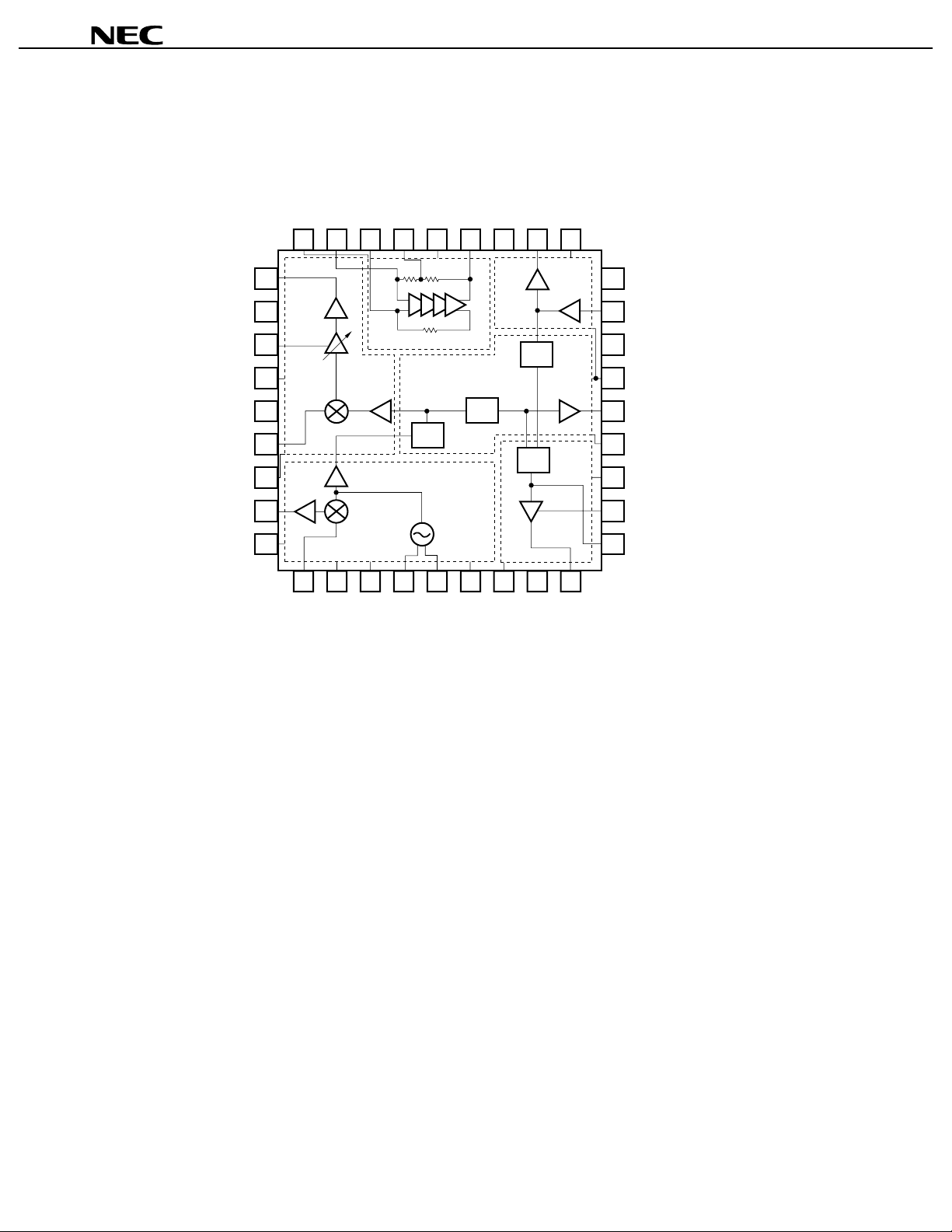
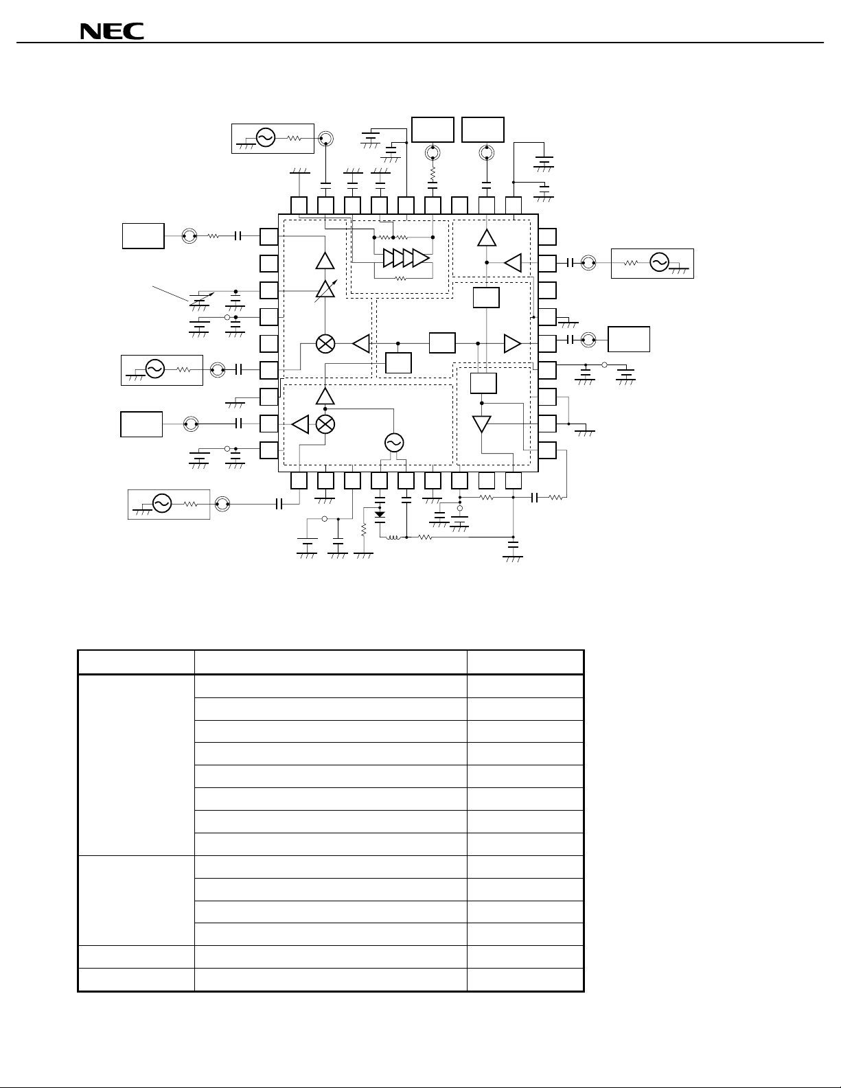
PIN CONNECTION AND INTERNAL BLOCK DIAGRAM
µµµµ
PB1005K
2ndIFin2
2ndIFin1
GND
(2ndIF-AMP)
27
26 25 24 23 22 21
IF-MIXout
(IF-MIX)
(IF-MIX)
IF-MIXin
(IF-MIX)
RF-MIXout
(RF-MIX)
28
29
N.C. REFin
GC
V
30
CC
V
31
N.C.
32
33
GND
34
35
V
CC
36
123456789
CC
V
GND
RF-MIXin
(RF-MIXin)
(1stLO-OSC)
CC
2ndIFbypass
V
(2ndIF-AMP)
÷
25
1stLO-OSC1
1stLO-OSC2
2ndIFout
N.C.
÷
8
CC
V
GND
(1stLO-OSC)
(phase detector)
÷
PD
20
2
CC
V
REFout
19
N.C.
PD-Vout3
(reference block)
18
N.C.
17
16
N.C.
GND
15
(divider block)
14
LOout
CC
V
13
(divider block)
GND
12
(Phase detector)
11
PD-Vout1
10
PD-Vout2
2
Preliminary Data Sheet P14016EJ1V0DS00

µµµµ
PB1005K
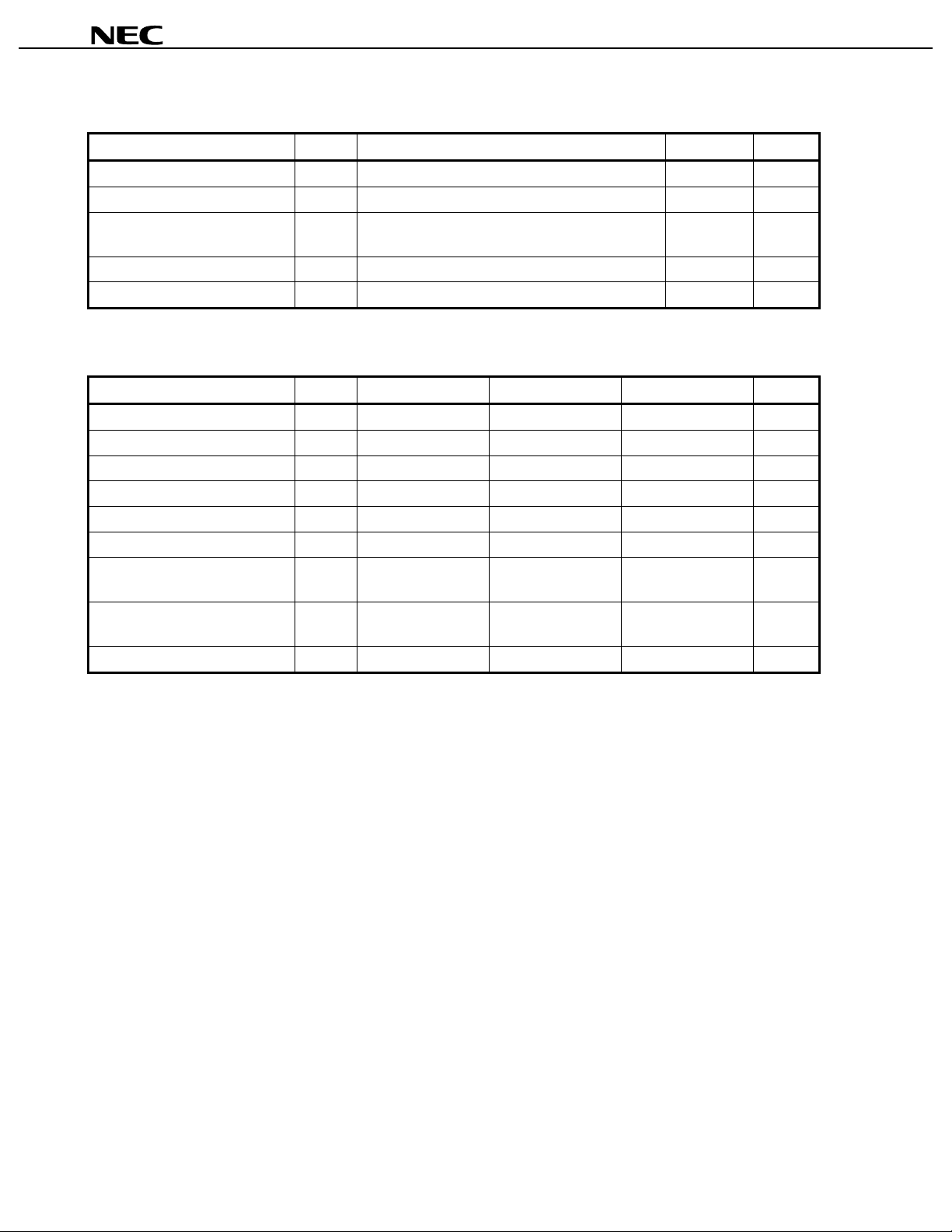
PRODUCT LINE-UP (TA = +25
Type Part Number
General
Purpose
Wideband
Separate
PC2756T 6-pin minimold
µ
PC2756TB
µ
PC2753GR IF down-convert er wi th gain
µ
IC
Clock
PB1003GS RF/IF down-converter
µ
Frequency
Specific
1 chip IC
PB1004GS
µ
PB1005GS
µ
PB1005K
µ
Notice
Typical performance. Please refer to ELECTRICAL CHARACTERISTICS in detail.
(Frequency unit: MHz)
RF down-converter with osc. Tr
control amplifier
+ PLL synthesizer
REF = 18.414
1stIF = 28.644/2ndIF = 1.023
RF/IF down-converter
+ PLL synthesizer
REF = 16.368
1stIF = 61.380/2ndIF = 4.092
C, VCC = 3.0 V)
°°°°
Functions
To know the associated products, please refer to their latest data sheets.
SYSTEM APPLICATION EXAMPLE
CC
V
(V)
2.7 to 3.3
2.7 to 3.3
2.7 to 3.3
2.7 to 3.3
2.7 to 3.3
CC
I
(mA)
CG
(dB)
Package Status
6.0 14
6-pin super minimold
6.5 60 to 79 20-pin plastic SSOP
(225 mil)
37.5 72 to 92
30-pin plastic SSOP
(300 mil)
37.5 72 to 92
45.0 72 to 92
36-pin plastic QFN
Available
Discontinued
Available
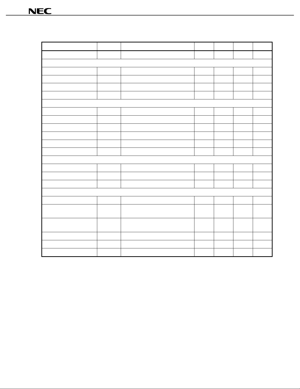
GPS receiver RF block diagram
60f0
BPF
IF-MIX
out
RF-MIX
1575.42 MHz
from
Antenna
LNA 1540f
µ
PC2749TBe.g.
BPF
0
1540f
0
OSC
RF-MIX
1600f
0
1stLO-OSC21stLO-OSC1
IF-MIX
1/25 1/8 P D
Caution This diagram schematically shows only the
This diagram does not present the actual application circuits.
0
40f
LOOP
AMP
8f0
LPF
V
CC
2ndlFbypass
2ndlF-Amp
1/2
REF
16f0
TCXO
16.368 MHz
IF-MIXout 2ndlFin1
in
V
GC
64f0
8f0
LOOUT
PB1005K’s internal functions on the system.
µµµµ
• f0 = 1.023 MHz in the diagram.
• PB1005K is in .
µ
2ndlFin2
4f0
16f
0
4.092 MHz
Buff
16.368 MHz
Buff
to Demodulator
to Demodulator
Preliminary Data Sheet P14016EJ1V0DS00
3
ABSOLUTE MAXIMUM RATINGS
Parameter Symbol Conditions Rating Unit
µµµµ
PB1005K
Supply Voltage V
Total Circuit Current I
Power Dissipation P
CC
TA = +25 °C3.6V
CC
TA = +25 °C 120 mA
D
Mounted on double-sided copper clad
50 × 50 × 1.6 mm epoxy glass P WB (T
Operating Ambient Temperature T
Storage Temperature T
A
stg
RECOMMENDED OPERATING RANGE
Parameter Symbol MIN. TYP. MAX. Unit
RFin
1stLOin
1stIFin
2ndLOin
2ndIFin
2ndIFout
f
REFin
REFout
f
LOout
CC
A
Supply Voltage V
Operating Ambient Temperature T
RF Input Frequency f
1st LO Oscillating Frequency f
1st IF Input Frequency f
2nd LO Input Frequency f
2nd IF Input/output Frequency f
Reference Input/output Frequency f
LO Output Frequency f
430 mW
A
= +85 °C)
40 to +85
−
55 to +150
−
C
°
C
°
2.7 3.0 3.3 V
40 +25 +85
−
1575.42
C
°
MHz
1616.80 1636.80 1656.80 MHz
61.38
65.472
4.092
16.368
8.184
MHz
MHz
MHz
MHz
MHz
4
Preliminary Data Sheet P14016EJ1V0DS00
µµµµ
PB1005K
ELECTRICAL CHARACTERISTICS (Unless otherwise specified TA = +25
C, VCC = 3.0 V)
°°°°
Parameter Symbol Conditions MIN. TYP. MAX. Unit
Total Circuit Current ICCtotal ICC1 + ICC2 + ICC3 + ICC4 32.0 45.0 60.0 mA
RF Down-converter Block (f
RFin
= 1575.42 MHz, f
1stLOin
= 1636.80 MHz, P
LOin
= −10 dBm, ZS = ZL = 50 Ω)
Circuit Current 1 ICC1 No Signals 6.0 10.0 14.0 mA
RF Conversion Gain CG
RF-SSB Noise Figure NF
Maximum IF Output P
IF Down-converter Block (f
O(sat)RF
1stIFIn
= 61.38 MHz, f
RF
RF
RFin
P
= −40 dBm 12.5 15.5 18.5 dB
RFin
P
= −40 dBm 7.0 10.0 13.0 dB
RFin
P
= −10 dBm
2ndLOIn
= 65.472 MHz, ZS = 50 Ω, ZL = 2 kΩ)
5.5
−
2.5 +0.5 dBm
−
Circuit Current 2 ICC2 No Signals 3.4 5.3 7.2 mA
IF Conversion Voltage Gain CG
IF-SSB Noise Figure NF
Maximum 2ndIF Output P
O(sat)IF
Gain Control Voltage V
Gain Control Range D
2nd IF Amplifier (f
2ndIF
= 4.092 MHz, ZS = 50 Ω, ZL = 2 kΩ)
(GV)IF
IF
GC
GC
at Maximum Gain, P
at Maximum Gain, P
at Maximum Gain, P
Voltage at Maximum Gain CG
1stIFin
P
= −50 dBm 20
1stIFin
= −50 dBm 38 41 44 dB
1stIFin
= −50 dBm 8.5 11.5 14.5 dB
1stIFin
= −20 dBm
IF
9.5
−
6.5
−
3.5 dBm
−
1.0 V
Circuit Current 3 ICC3 No Signals 1.55 2.40 3.25 mA
Voltage Gain G
Output Power P
2ndIFout
V
2ndIFin
P
= −60 dBm 37 40 43 dB
2ndIFin
P
= −30 dBm
−
14.5
−
11.5
−
8.5 dBm
PLL Synthesizer Block
Circuit Current 4 ICC4 PLL All Block Operati ng 18.5 28.5 38.5 mA
Phase Comparing
PD
f
PLL Loop 8.0 8.184 8.4 MHz
Frequency
Reference Input Minimum
V
REFin
ZL = 10 kΩ//20 pF
Note
200
Level
Loop Filter Output Level (H) V
Loop Filter Output Level (L) V
Reference Output Swing V
LP(H)
LP(L)
REFout
ZL = 10 kΩ//2 pF
Note
2.8
1.0
0.4 V
mV
V
dB
P-P
V
P-P
Impedance of measurement equipment
Note
Preliminary Data Sheet P14016EJ1V0DS00
5

µµµµ
PB1005K
STANDARD CHARACTERISTICS (Unless otherwise specified TA = +25
Parameter Symbol Conditions Reference Unit
RF Down-converter Block (P
LO Leakage to IF Pin LO
LO Leakage to RF Pin LO
Input 3rd Order Intercept
Point
IF Down-converter Block (1st LO oscillating, ZS = 50 Ω, ZL = 2 kΩ)
LO Leakage to 2nd IF LO
LO Leakage to 1st IF LO
Input 3rd Order Intercept
Point
VCO Block
Phase Noise C/N PLL Loop, ∆1kHz of VCO wave
1stLOin
= −10 dBm, ZS = ZL = 50 Ω)
if
1stLOin
f
rf
1stLOin
f
IIP3RF f
2ndif
1stif
IIP3IF f
RFin
1 = 1 600 MHz, f
1stLOin
f
2ndLOin
f
2ndLOin
f
1stIFin
2ndLOin
f
= 1 636.80 MHz
= 1 636.80 MHz
= 1 660 MHz
= 65.472 MHz
= 65.472 MHz
1 = 61.38 MHz, f
= 65.472 MHz
RFin
2 = 1605 MHz
1stIFIn
2 = 61.48 MHz
C, VCC = 3.0 V)
°°°°
30 dBm
−
30 dBm
−
13 dBm
−
20 dBm
−
40 dBm
−
34 dBm
−
78 dBc/Hz
−
6
Preliminary Data Sheet P14016EJ1V0DS00

PIN EXPLANATION
µµµµ
PB1005K
Pin
No.
Pin Name
35 RX-MIXout
36 VCC (RF-MIX) 2.7 to 3.3
1RF-MIXin
2 GND (RF-MIX) 0
CC
3V
(1stLO-OSC)
41stLO-OSC1
51stLO-OSC2
6GND
(1stLO-OSC)
7VCC (phase
detector)
8N.C.
9 PD-Vout3 Pull-up
10 PD-Vout2
11 PD-Vout1 Pull-up
12 GND (phase
detector)
Applied
Voltage
(V)
2.7 to 3.3
0
2.7 to 3.3
with
resistor
with
resistor
0
Pin
Voltage
(V)
1.68 Output pin of RF mixer.
1.20 Input pin of RF mixer.
1.88
1.88
Output in
accordance
with phase
difference
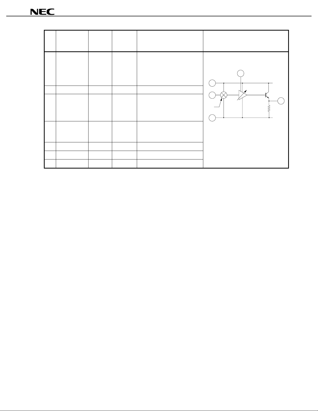
Function and Application Internal E qui valent Circuit
1st IF filter mus t be inserted
between pin 33 & 35.
Supply voltage pin of RF mixer
block. This pin must be
decoupled with capacitor
(example: 1 000 pF).
1 575.42 MHz band pass filter
can be inserted between pin 1
and external LNA.
Ground pin RF mixer.
Supply voltage pin of dif ferential
amplifier for 1st LO oscillator
circuit.
Pin 4 & 5 are each base pin of
differential amplifi er f or 1st LO
oscillator. These pins should be
equipped with LC and varactor
to oscillate on 1 636.80 MHz as
VCO.
Ground pin of differential
amplifier for 1st LO oscillator
circuit.
Supply voltage pin of phase
detector and active loop f i l ter.
Non connection
Pins of active loop filter for
tuning voltage output.
The active transist ors
configured with darlington pair
are built on chip. Pin 11 should
be pulled down with external
resistor. Pin 9 to 10 s houl d be
equipped with external RC in
order to adjust dumping factor
and cutoff frequency. Thi s
tuning voltage output must be
connected to varactor diode of
1st LO-OSC.
Ground pin of phase detector +
active loop filter.
36
1stLO
-OSC
1
3
4 5
6
7
PD
12
V
35
2
CC
RF-MIX or
Prescaler
input
10
9
11
Preliminary Data Sheet P14016EJ1V0DS00
7

µµµµ
PB1005K
Pin
13 V
Pin Name
CC
No.
(divider block)
14 LOout
15 GND
(divider block)
16 N.C.
17 REFin
18 N.C.
CC
19 V
(reference
block)
20 REFout
21 N.C.
22 2ndIFout
CC
23 V
(2ndIF-AMP)
24 2ndIF bypass
25 2ndIFin2
26 2ndIFin1
27 GND
(2ndIF-AMP)
Applied
Voltage
(V)
2.7 to 3.3
0
Pin
Voltage
(V)
2.08 Monitor pin of comparison
1.96 Input pin of reference frequency.
2.7 to 3.3
1.65 Output pin of reference
2.7 to 3.3
0
1.56 Output pin of 2nd IF amplifier.
2.30 Bypass pin of 2nd IF amplif i er
2.35 Pin of 2nd IF amplifier input 2.
2.35 Pin of 2nd IF amplifier input 1.
Function and Application Internal E qui valent Circuit
Supply voltage pin of
prescalers.
frequency at phase detect or.
Ground pin of prescalers +
LOout amplifier
Non connection
13
1st
LO
OSC
15
IF
MIX
÷
25÷8
PD PD
This pin should be equipped
with external 16.368 MHz
oscillator (example: TCXO).
19
Non connection
Supply voltage pin of
input/output amplifiers in
P-P
17
15
reference block.
frequency. The frequency from
pin 17 can be took out as 1 V
swing.
Non connection
This pin output 4.092 MHz
clipped sinewave.
This pin should be equipped
with external inverter to adj ust
level to next stage on us er’ s
23
system.
Supply voltage pin of 2nd IF
24
amplifier.
26
input 1. This pin should be
25
grounded through capacitor.
This pin should be grounded
27
through capacitor.
2nd IF filter can be insert ed
between pin 26 & 28.
Ground pin of 2nd IF amplifier.
14
÷
2
Ref.
20
PD
22
8
Preliminary Data Sheet P14016EJ1V0DS00
µµµµ
PB1005K
Pin
No.
Pin Name
28 IF-MIXout
29 N.C.
30 VGC (IF-MIX) 0 to 3.3
31 VCC (IF-MIX) 2.7 to 3. 3
32 N.C.
33 IF-MIXin
34 GND (IF-MIX) 0
Applied
Voltage
(V)
Pin
Voltage
(V)
1.15 Output pin from IF mixer.
2.00 Input pin of IF mixer.
Function and Application Internal E qui valent Circuit
IF mixer output signal goes
through gain control amplifier
before this emitter fol l ower
output port.
Non connection
Gain control voltage pin of I F
mixer output amplifier. This
voltage performs forward cont rol
GC
(V
up → Gain down).
Supply voltage pin of IF m i xer,
gain control amplifier and
emitter follower transistor.
Non connection
Ground pin of IF mixer.
30
31
33
2nd
LO
34
Caution Ground pattern on the board must be formed as wide as possible to minimize ground
impedance.
28
Preliminary Data Sheet P14016EJ1V0DS00
9
TEST CIRCUIT
µµµµ
PB1005K
Spectrum
Analyzer
To get maximum gain.
Apply 1.0V MAX.
CC
50 Ω
Signal Generator
Spectrum
Analyzer
CC
50 Ω
Signal Generator
Signal Generator
C21R6
C22
C23V
C1
C2
C3V
÷
V-Di
L
25
C7
Spectrum
Analyzer
R5
C16C18
÷
8
C8
R2
50 Ω
27
28
29
30
31
32
33
34
35
36
123456789
C4
V
CC
V
CC
C17
C19C20
26 25 24 23 22 21 20 19
C6
R1
C5
Osilloscope
C15
V
CC
PD
V
CC
C14
18
17
C13
C10
C9
16
15
14
13
12
11
10
C12
C11
R4
÷
2
R3
50 Ω
Signal Generator
Osilloscope
V
CC
Spectrum Analyzer : measure frequency
Oscilloscope : measure output voltage swing
Component List
Form Symbol Value
Chip capacitor
Chip resistor
Varactor Diode V-Di 1SV285
Chip Inductor L 3.9 nH
C1 to C5, C8, C11 to C15, C17, C18, C22 1 000 pF
C6, C7 24 pF (UJ)
C9 1800 pF
C10 33 nF
C19 10 000 pF
C23 1 µF
C16, C20 0.1 µF
C21 0.01
R1, R2 4.7 k
R3 6.2 k
R4 1.2 k
R5, R6 1.95 k
F
µ
Ω
Ω
Ω
Ω
10
Preliminary Data Sheet P14016EJ1V0DS00

PACKAGE DIMENSIONS
36 PIN PLASTIC QFN (UNIT: mm)
6.2±0.2
µµµµ
PB1005K
4–C0.5
Pin36
Pin1
6.0±0.2
6.2±0.2
6.0±0.2
6.0±0.2
1.0MAX
6.2±0.2
6.2±0.2
6.0±0.2
0.22±0.05 0.6±0.1
Preliminary Data Sheet P14016EJ1V0DS00
0.5±0.025
Bottom View
11

µµµµ
PB1005K
NOTE ON CORRECT USE
(1) Observe precautions for handling because of electro-static sensitive devices.
(2) Form a ground pattern as widely as possible to minimize ground impedance (to prevent abnormal oscillation).
(3) Keep the track length of the ground pins as short as possible.
(4) Connect a bypass capacitor (example: 1 000 pF) to the VCC pin.
(5) Frequency signal input/output pins must be each coupled with external capacitor for DC cut.
RECOMMENDED SOLDERING CONDITIONS
This product should be soldered under the following recommended conditions. For soldering methods and
conditions other than those recommended below, contact your NEC sales representative.
Soldering Method Soldering Conditions Recommended Condition Sy m bol
Infrared Reflow Pac kage peak temperature: 235 °C or below
Time: 30 seconds or less (at 210 °C)
Count: 2, Exposure limi t
Partial Heating Pin temperature: 300 °C
Time: 3 seconds or less (per side of device)
Exposure limit
After opening the dry pack, keep it in a place below 25 °C and 65 % RH for the allowable storage period.
Note
Note
: None
Note
: None
IR35-00-2
–
Caution Do not use different soldering methods together (except for partial heating).
For details of recommended soldering conditions for surface mounting, refer to information document
SEMICONDUCTOR DEVICE MOUNTING TECHNOLOGY MANUAL (C10535E).
12
Preliminary Data Sheet P14016EJ1V0DS00

[MEMO]
µµµµ
PB1005K
Preliminary Data Sheet P14016EJ1V0DS00
13

[MEMO]
µµµµ
PB1005K
14
Preliminary Data Sheet P14016EJ1V0DS00

[MEMO]
µµµµ
PB1005K
Preliminary Data Sheet P14016EJ1V0DS00
15

µµµµ
PB1005K
ATTENTION
OBSERVE PRECAUTIONS
FOR HANDLING
ELECTROSTATIC
SENSITIVE
DEVICES
NESAT (NEC Silicon Advanced Technology) is a trademark of NEC Corporation.
• The information in this document is subject to change without notice. Before using this document, please
confirm that this is the latest version.
• No part of this document may be copied or reproduced in any form or by any means without the prior written
consent of NEC Corporation. NEC Corporation assumes no responsibility for any errors which may appear in
this document.
• NEC Corporation does not assume any liability for infringement of patents, copyrights or other intellectual property
rights of third parties by or arising from use of a device described herein or any other liability arising from use
of such device. No license, either express, implied or otherwise, is granted under any patents, copyrights or other
intellectual property rights of NEC Corporation or others.
• Descriptions of circuits, software, and other related information in this document are provided for illustrative
purposes in semiconductor product operation and application examples. The incorporation of these circuits,
software, and information in the design of the customer's equipment shall be done under the full responsibility
of the customer. NEC Corporation assumes no responsibility for any losses incurred by the customer or third
parties arising from the use of these circuits, software, and information.
• While NEC Corporation has been making continuous effort to enhance the reliability of its semiconductor devices,
the possibility of defects cannot be eliminated entirely. To minimize risks of damage or injury to persons or
property arising from a defect in an NEC semiconductor device, customers must incorporate sufficient safety
measures in its design, such as redundancy, fire-containment, and anti-failure features.
• NEC devices are classified into the following three quality grades:
"Standard", "Special", and "Specific". The Specific quality grade applies only to devices developed based on a
customer designated "quality assurance program" for a specific application. The recommended applications of
a device depend on its quality grade, as indicated below. Customers must check the quality grade of each device
before using it in a particular application.
Standard: Computers, office equipment, communications equipment, test and measurement equipment,
audio and visual equipment, home electronic appliances, machine tools, personal electronic
equipment and industrial robots
Special: Transportation equipment (automobiles, trains, ships, etc.), traffic control systems, anti-disaster
systems, anti-crime systems, safety equipment and medical equipment (not specifically designed
for life support)
Specific: Aircraft, aerospace equipment, submersible repeaters, nuclear reactor control systems, life
support systems or medical equipment for life support, etc.
The quality grade of NEC devices is "Standard" unless otherwise specified in NEC's Data Sheets or Data Books.
If customers intend to use NEC devices for applications other than those specified for Standard quality grade,
they should contact an NEC sales representative in advance.
M7 98. 8
 Loading...