

DATA SHEET
SILICON TRANSISTOR ARRAY
µ
NPN SILICON POWER TRANSISTOR ARRAY
LOW SPEED SWITCHING USE
INDUSTRIAL USE
PA1454
DESCRIPTION
The µPA1454 is NPN silicon epitaxial Power Transistor
Array that built in 4 circuits designed for driving solenoid,
relay, lamp and so on.
FEATURES
• Easy mount by 0.1 inch of terminal interval.
• High hFE. Low VCE(sat).
FE = 800 to 3200 (at IC = 1 A)
h
CE(sat) = 1.0 V MAX. (at IC = 3 A)
V
ORDERING INFORMATION
Part Number Package Quality Grade
µ
PA1454H 10 Pin SIP Standard
Please refer to "Quality grade on NEC Semiconductor Devices"
(Document number IEI-1209) published by NEC Corporation to
know the specification of quality grade on the devices and its
recommended applications.
ABSOLUTE MAXIMUM RATINGS (Ta = 25 ˚C)
Collector to Base Voltage VCBO 100 V
Collector to Emitter Voltage V
Emitter to Base Voltage V
Collector Current (DC) I
Collector Current (pulse) I
Base Current (DC) I
Total Power Dissipation P
Total Power Dissipation P
Junction Temperature T
Storage Temperature T
CEO 100 V
EBO 7V
C(DC) 5 A/unit
C(pulse)* 10 A/unit
B(DC) 1.0 A/unit
T1** 3.5 W
T2*** 28 W
j 150 ˚C
stg –55 to +150 ˚C
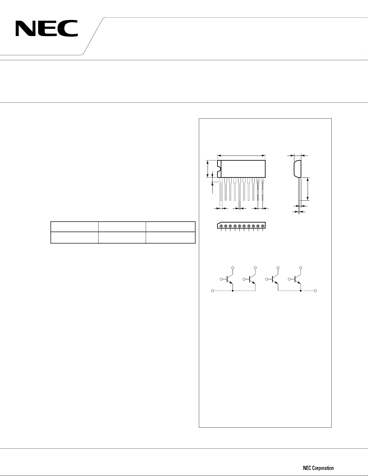
PACKAGE DIMENSION
(in millimeters)
26.8 MAX.
10
2.5
1.4 0.6 ±0.1
1 2 3 4 5 6 7 8 9 10
CONNECTION DIAGRAM
3
2
110
4
2, 4, 6, 8
3, 5, 7, 9
1, 10
2.54
5
6
PIN No.
: Base (B)
: Collector (C)
: Emitter (E)
4.0
10 MIN.
1.4
0.5 ±0.1
7
9
8
* PW ≤ 300
** 4 Circuits, T
*** 4 Circuits, T
Document No. IC-3520
Date Published September 1994 P
Printed in Japan
µ
s, Duty Cycle ≤ 10 %
a = 25 ˚C
c = 25 ˚C
The information in this document is subject to change without notice.
©
1994
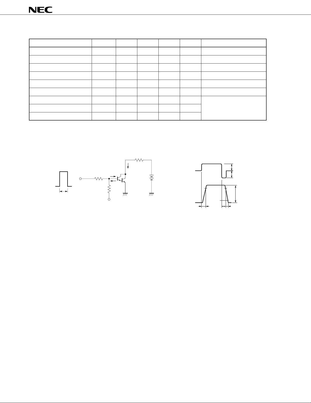
ELECTRICAL CHARACTERISTICS (Ta = 25 ˚C)
CHARACTERISTIC SYMBOL MIN. TYP. MAX. UNIT TEST CONDITIONS
Collector Leakage Current ICBO 10
Emitter Leakage Current IEBO 10
DC Current Gain hFE1
DC Current Gain hFE2
Collector Saturation Voltage VCE(sat)
Base Saturation Voltage VBE(sat)
*
800 1300 3200 — VCE = 5 V, IC = 1 A
*
500 1000 — VCE = 5 V, IC = 3 A
*
*
1.0 V IC = 3 A, IB = 30 mA
1.2 V IC = 3 A, IB = 30 mA
Turn On Time ton 1
Storage Time tstg 3
Fall Time tf 1.5
µ
A VCB = 100 V, IE = 0
µ
A VEB = 7 V, IC = 0
µ
s
IC = 3 A
µ
µ
IB1 = –IB2 = 30 mA
s
s
.
VCC = 50 V, RL = 16.7 Ω
.
See test circuit
* PW ≤ 350 µs, Duty Cycle ≤ 2 % / pulsed
SWITCHING TIME TEST CIRCUIT
.
R
L
= 16.7 Ω
.
µ
PA1454
.
.
V
IN
PW
.
PW = 50 s
µ
.
Duty Cycle ≤ 2 %
V
BB
1
B1
1
B2
.
= –5 V
.
C
I
T.U.T.
CC
V
.
= 50 V
.
Base Current
Wave Form
Collector
Current
Wave Form
I
B1
I
B2
90 %
I
C
10 %
tft
t
on
stg
2

TYPICAL CHARACTERISTICS (Ta = 25 ˚C)
DERATING CURVE OF SAFE
OPERATING AREA
100
80
60
S/b Limited
Dissipation Limited
100
50
10
5
SAFE OPERATING AREA
IC(pulse) MAX.
IC(DC) MAX.
µ
PA1454
1 ms
10 ms
50 ms
PW =
100 s
300 s
µ
µ
40
20
dT - Percentage of Rated Current - %
0
50 100 150
C - Case Temperature - ˚C
T
TOTAL POWER DISSIPATION vs.
AMBIENT TEMPERATURE
NEC
PA1454
µ
4
3
2
PT - Total Power Dissipation - W
1
25 50 75 100 125 150
0
a - Ambient Temperature - ˚C
T
4 Circuits Operation
3 Circuits Operation
2 Circuits Operation
1 Circuit Operation
1
IC - Collector Current - A
0.5
TC = 25 ˚C
Single Pulse
0.1
1
V
CE - Collector to Emitter Voltage - V
5 100
TOTAL POWER DISSIPATION vs.
CASE TEMPERATURE
30
20
10
PT - Total Power Dissipation - W
25 50 75 100 125 150
0
C - Case Temperature - ˚C
T
VCEO MAX.
10 50
4 Circuits Operation
3 Circuits Operation
2 Circuits Operation
1 Circuit Operation
DC CURRENT GAIN vs. COLLECTOR CURRENT
10000
1000
100
hFE - DC Current Gain
10
0.001
CE = 5 V
V
Pulsed
0.01 0.1 1 10
I
C - Collector Current -A
BASE AND COLLECTOR SATURATION
VOLTAGE vs. COLLECTOR CURRENT
10
1
V
C
I
0.1
BE(sat) - Base Saturation Voltage - V
VCE(sat) - Collector Saturation Voltage - V
V
0.02
0.01
= 200·I
C
I
BE(sat)
B
= 1000·I
B
= 500·I
C
I
0.1 1 10
IC - Collector Current - A
B
= 200·I
C
I
B
= 100·I
C
I
B
CE(sat)
V
3

µ
g
PA1454
100
10
Rth (j-c) - Transient Thermal Resistance - ˚C/W
TRANSIENT THERMAL RESISTANCE
1
0.1
1 10 100
PW - Pulse Width - ms
V
CE ≤ 10 V
COLLECTOR CURRENT vs. COLLECTOR TO
EMITTER VOLTAGE
6
5
4
3
2
IC - Collector Current - A
1
0
12345
V
CE - Collector to Emitter Volta
50
20
10
5
2
1.5
IB = 0.5 mA
e - V
1
4

µ
PA1454
REFERENCE
Document Name Document No.
NEC semiconductor device reliability/quality control system. TEI-1202
Quality grade on NEC semiconductor devices. IEI-1209
Semiconductor device mounting technology manual. IEI-1207
Semiconductor device package manual. IEI-1213
Guide to quality assurance for semiconductor devices. MEI-1202
Semiconductor selection guide. MF-1134
5

[MEMO]
µ
PA1454
No part of this document may be copied or reproduced in any form or by any means without the prior written
consent of NEC Corporation. NEC Corporation assumes no responsibility for any errors which may appear in this
document.
NEC Corporation does not assume any liability for infringement of patents, copyrights or other intellectual
property rights of third parties by or arising from use of a device described herein or any other liability arising
from use of such device. No license, either express, implied or otherwise, is granted under any patents,
copyrights or other intellectual property rights of NEC Corporation or others.
The devices listed in this document are not suitable for use in aerospace equipment, submarine cables, nuclear
reactor control systems and life support systems. If customers intend to use NEC devices for above applications
or they intend to use "Standard" quality grade NEC devices for applications not intended by NEC, please contact
our sales people in advance.
Application examples recommended by NEC Corporation
Standard: Computer, Office equipment, Communication equipment, Test and Measurement equipment,
Machine tools, Industrial robots, Audio and Visual equipment, Other consumer products, etc.
Special: Automotive and Transportation equipment, Traffic control systems, Antidisaster systems, Anticrime
systems, etc.
M4 92.6
 Loading...