NEC UPB1505GR-E1, UPB1505GR Datasheet

DATA SHEET
BIPOLAR DIGITAL INTEGRATED CIRCUIT
µ
PB1505GR
3.0 GHz PRESCALER DIVIDED BY 256, 128, 64
FOR BS/CS TUNER
DESCRIPTION
µ
PB1505GR is a silicon prescaler IC operating up to 3.0 GHz and divided by 256, 128, 64. Due to 3.0 GHz operation and
high division, this IC can contribute to produce BS/CS tuners with kit-use of 17K series DTS controller or standard CMOS
PLL IC. The package is 8 pin plastic SOP suitable for surface mounting.
This IC is manufactured using NEC’s 20 GHz f
passivation film and gold electrodes. These materials can protect the chips from external pollution and prevent corrosion/
migration. Thus, this IC has with excellent performance, uniformity and reliability.
T NESAT
III silicon bipolar process. This process uses silicon nitride
FEATURES
• High toggle-frequency : 0.5 GHz to 3.0 GHz
• Low power-consumption : 14 mA TYP. at 5 V
• High divide-ratio : ÷256, ÷128, ÷64
• High input-sensitivity : –14 to +10 dBm @ 1.0 GHz to 2.7 GHz
• Wide output-swing : 1.6 Vp-p (CL = 8 pF load)
ORDERING INFORMATION
PART NUMBER PACKAGE SUPPLYING FORM
µ
PB1505GR-E1
Remarks To order evaluation samples, please contact your local NEC sales office. (Order number : µPB1505GR)
8 pin plastic SOP Embossed tape 12 mm wide. QTY 2.5 k/reel
(225 mil) Pin 1 is in tape pull-out direction.
PIN ASSIGNMENT (Top View)
IN
1
V
2
CC
8
IN
7
GND
The information in this document is subject to change without notice. Before using this document, please
confirm that this is the latest version.
Not all devices/types available in every country. Please check with local NEC representative for availability
and additional information.
Document No. P10872EJ3V0DS00 (3rd edition)
Date Published October 1999 N CP(K)
Printed in Japan
SW1
OUT
3
4
Caution electro-static sensitive devices
The mark shows major revised points.
6
5
SW2
GND
©
1996,1999

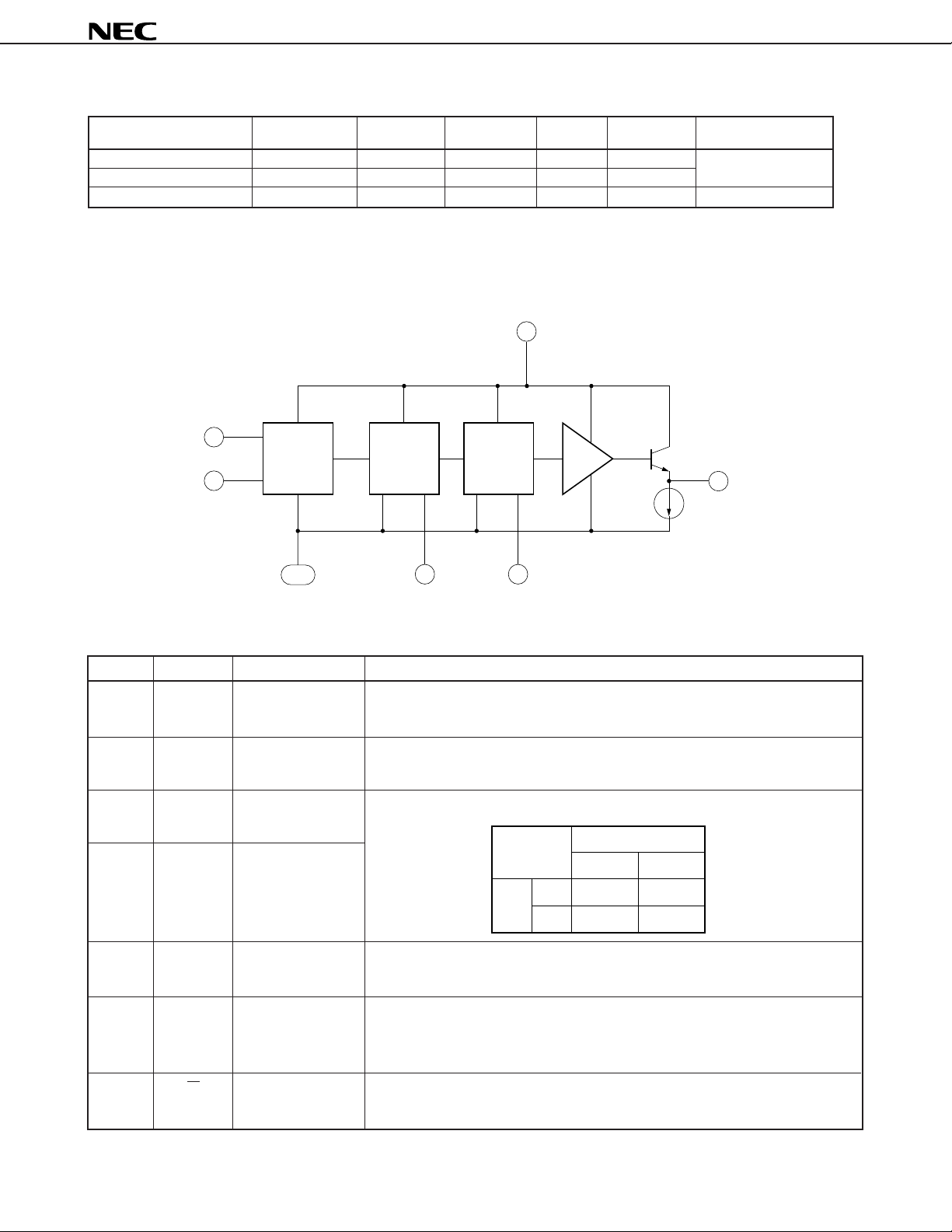
SELECTOR GUIDE
µ
PB1505GR
FEATURES
2.5 GHz / ÷512, ÷256
2.5 GHz / ÷128, ÷64
3.0 GHz / ÷256, ÷128, ÷64
PRODUCT ICC fin VCC
NUMBER (mA) (GHz) (V)
µ
PB586G 28 0.5 to 2.5 5 8 pin SOP
µ
PB588G 26 0.5 to 2.5 5 8 pin SOP
µ
PB1505GR 14 0.5 to 3.0 5 8 pin SOP Typical of prescaler
Notice Typical performance. Please refer to Electrical Characteristics in detail.
To know the associated products, please refer to their latest data sheets.
INTERNAL BLOCK DIAGRAM
CC
V
2
INPUT
BYPASS
1
1 / 64 1 / 2 1 / 2 Buff.
8
5, 7
GND SW1 SW2
36
PACKAGE PIN ASSIGNMENT
NEC original
OUTPUT
4
PIN DESCRIPTIONS
PIN NO. SYMBOL ASSIGNMENT FUNCTIONS AND EXPLANATION
1 IN Frequency input
pin
2VCC Power supply pin
3 SW1 Divided ratio
control input pin 1
6 SW2 Divided ratio
control input pin 2
4 OUT Divided frequency
output pin
5 GND Ground pin
7
Input frequency from an external VCO output.
Must be coupled with capacitor (e.g. 1 000 pF) for DC cut.
Supply voltage 5.0±0.5 V for operation. Must be connected bypass capacitor
(e.g. 1 000 pF) to minimize ground impedance.
Divided ratio control can be governed by following input data to these pins.
SW2
HL
SW1
H
L
This frequency output can be interfaced to CMOS PLL.
Must be coupled with capacitor (e.g. 1 000 pF) for DC cut.
This pin must be connected to the system ground with minimum inductance.
Ground pattern on the board should be formed as wide as possible.
(Track length should be kept as short as possible.)
1/64 1/128
1/128
1/256
8 IN Frequency-input
bypass pin
2
This pin must be connected bypass capacitor (e.g. 1 000 pF) to minimize ground
impedance.
Data Sheet P10872EJ3V0DS00

ABSOLUTE MAXIMUM RATINGS
PARAMETER SYMBOL RATING UNIT CONDITIONS
Supply voltage VCC –0.5 to +6 V TA = +25 °C
Input voltage VIN –0.5 to VCC +0.5 V TA = +25 °C
µ
PB1505GR
Power dissipation PD 250 mW
Operating temperature Topt –40 to +85 °C
Storage temperature Tstg –55 to +150 °C
Mounted on 50 × 50 × 1.6 mm double copper clad
epoxy glass PWB (TA = +85 °C)
RECOMMENDED OPERATING RANGE
PARAMETER SYMBOL MIN. TYP. MAX. UNIT
Supply voltage VCC 4.5 5.0 5.5 V
Operating temperature Topt –40 +25 +85 °C
ELECTRICAL CHARACTERISTICS (TA = –40 to +85 °C, VCC = 4.5 to 5.5 V)
PARAMETER SYMBOL MIN. TYP. MAX. UNIT CONDITIONS
Circuit current ICC 9.0 14.0 19.5 mA No input signal
Upper response frequency 1 fin(U)1 3.0 GHz Pin = –10 to +10 dBm
Upper response frequency 2 fin(U)2 2.7 GHz Pin = –14 to –10 dBm
Lower response frequency 1 fin(L)1 0.5 GHz Pin = –10 to +8 dBm
Lower response frequency 2 fin(L)2 1.0 GHz Pin = –14 to –10 dBm, +8 to +10 dBm
Input sensitivity 1 Pin1 –10 +8 dBm fin = 0.5 to 1.0 GHz
Input sensitivity 2 Pin2 –14 +10 dBm fin = 1.0 to 2.7 GHz
Input sensitivity 3 Pin3 –10 +10 dBm fin = 2.7 to 3.0 GHz
Output Swing VOUT 1.3 1.6 VP-P CL = 8 pF
SW1 input voltage (H) VIH1 VCC VCC VCC V
SW1 input voltage (L) VIL1 OPEN OPEN OPEN V
SW2 input voltage (H) VIH2 VCC VCC VCC V
SW2 input voltage (L) VIL2 OPEN OPEN OPEN V
Data Sheet P10872EJ3V0DS00
3
 Loading...