

1
Cover Sheet
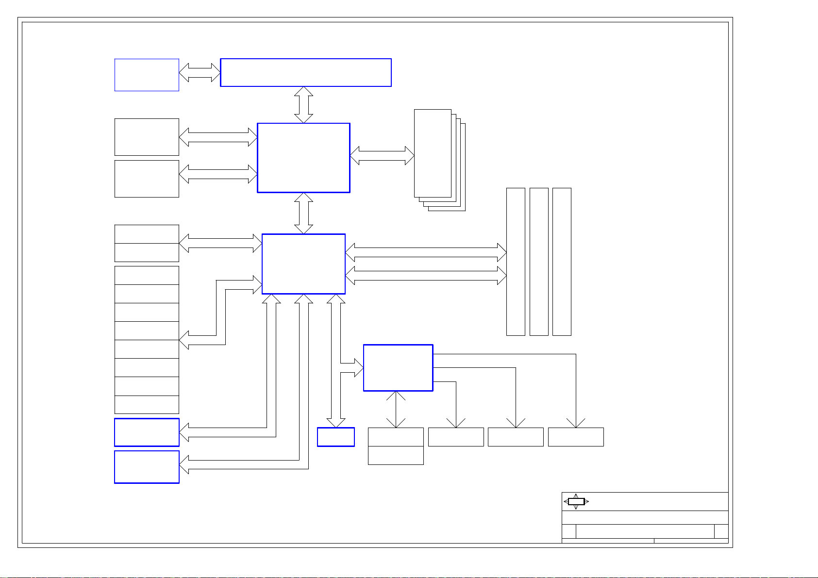
Block Diagram
Revision History 1 - 3
Intel mPGA478B CPU - Signals
1
2
3 - 5
6
VISE (MS-6715)
Intel (R) Springdale (GMCH) + ICH5 Chipset
Version 0A
09/25/2002 Initial
Intel Northwood & Prescott mPGA478B Processor
Intel mPGA478B CPU - Power
Intel Springdale - Host Signals
Intel Springdale - Memory Signals
Intel Springdale - AGP & LDT Signals
Intel ICH5 - PCI & IDE & AC97 Signals
Intel ICH5 - Other Signals
Clock - ICS ICS952606 & FWH & Manual
LPC I/O - LPC47B387
AC97 Audio - AD1981B
A A
Broadcom BCM5702
DDR System Memory 1 & 2
DDR System Memory 3 & 4
7
8
9
10
11
12
13
14
15
16
17
18
CPU:
Intel Northwood/Prescott - 3.0G & Above
System Chipset:
Intel Springdale - GMCH (North Bridge)
Intel ICH5 (South Bridge)
On Board Chipset:
BIOS -- FWH EEPROM
AC'97 Codec -- AD1981B
LPC Super I/O -- LPC47B387
LAN -- CSR Interface
CLOCK -- ICS952606 / CY28405
H/W Monitoring -- ADM1027
AGP 4X/8X Slot & PCI Riser Card
PCI Slots 1 & 2 & 3
ATA33/66/100 IDE & Video Connectors
USB & LAN Connectors
H/W Monitor & FAN
ATX & Front Panel
AGP & MEMORY & USB Regulator Controller
VCC_DAC & VTT Regulator & VR Thermal
VRM 10 - Intersil HIP 6556B + HIP 6602B
PULL UP/ DOWN RESISTORS
GPIO
19
20
21
22
23
24
25
26
27
28
29
Main Memory:
DDR2700 * 4 (Max 4GB)
Expansion Slots:
PCI2.3 SLOT * 3
AGP4X/8X SLOT * 1
Intersil PWM:
Controller: HIP6556B
Driver: HIP6602B * 2
Regulators
System : FAN5236
1
MSI
Title
Size Document Number Rev
Date: Sheet of
MICRO-STAR INt'L CO., LTD.
H/W Project Leader : Andy Chen
H/W Project Engineer : Prudence Wang
COVER SHEET
VISE (MS-6715)
1 30Friday, September 27, 2002
0A
1
VRM 10
Intersil 6556
Intel mPAG478B Processor
Block Diagram
4-Phase PWM
FSB
64bit DDR
133/166MHz@2.1/2.7GB/s
4 DDR
DIMM
Modules
AGP 1.5V
Connector
Analog
133/166MHz@4.2/4.5GB/s
4X/8X w/Fast Write
66MHz@2.1GB/s
Springdale
Video
Out
HCT
ICH5
Link
PCI CNTRL
PCI ADDR/DATA
33MHz@133MB/s
PCI Slot 1
PCI Slot 2
PCI Slot 3
66MHz@266MB/s
UltraDMA
IDE Primary
IDE Secondary
A A
USB Port 0
33/66/100/133
44.44MHz(W)/50MHz(R)@88.9/100MB/s
USB Port 1
USB Port 2
USB Port 3
USB Port 4
USB
240MHz@60MB/s
LPC Bus
33MHz@16.5MB/s
LPC SIO
USB Port 5
SMSC
LPC47B387
USB Port 6
USB Port 7
AD1981B
AC'97 Codec
GIGA LAN
BCM5702
AC'97 Link
12.288MHz@1.536MB/s
PCI
33MHz@133MB/s
Flash
Keyboard
Mouse
1
Floopy Parallel Serial
MSI
Title
Size Document Number Rev
Date: Sheet of
MICRO-STAR INt'L CO., LTD.
H/W Project Leader : Andy Chen
H/W Project Engineer : Prudence Wang
BLOCK DIAGRAM
VISE (MS-6715)
2 30Friday, September 27, 2002
0A

5
Revision Initial ver: 0AE0 on 07/31/2002
Schematic Initial on July 31.
Revision change list from ver: 0AE0 to ver: 0AE1 on 08/01/2002
Sheet 1: Modify some txts.
Sheet 2: Modify some txts.
Sheet 16: Move Lan connector to page 26.
D D
Sheet 25: Modify some block for customer request, detail list on below:
(1) Modify 5v USB power supplier.
(2) Modify 5V main power circuit.
(3) Modify GMCH VTT voltage supplier.
(4) Add GMCH VTT reference voltage circuit.
Sheet 26: Modify some block for customer request, detail list on below:
(1) Modify 3V standby power supplier.
(2) Change VTT_DDR to LP2995.
(3) Add lan magnetic circuit.
(4) Modify Lan connector.
(5) Add 1.5V standby voltage.
Revision change list from ver: 0AE1 to ver: 0AE2 on 08/09/2002
Sheet 8: Change VTT_FSB to capacitors termination on pin A15 and A21.
Sheet 9: Change VCC_DDR to capacitors termination on pin
C C
E35,E35,AA35,AR21 and AR15.
Sheet 27: Change some bulk caps from 2200uF to 560uF.
Revision change list from ver: 0AE2 to ver: 0AE3 on 08/13/2002
Sheet 12: Modify some block for customer request, detail list on below:
(1) Delete GP14 and GP15 on pin U21 and pin T20 on ICH5.
(2) Add CHASIS_ID2 on pin V3 on ICH5.
(3) Delete USB6+, USB6-, USB7+, and USB7-.
(4) Change FRONT_USB_DET# from pin C13 to pin D13 on ICH5.
Sheet 13: Modify some block for customer request, detail list on below:
(1) Modify clock generator library.
(2) Change PCI clock label.
(3) Add strapping resistors.
Sheet 17: Delete some caps on VCC_DDR.
Sheet 18: Delete some caps on VCC_DDR.
B B
Sheet 19: Delete some AGP termination resistors.
Sheet 20: Change PCI clock label.
Sheet 22: Modify some block for customer request, detail list on below:
(1) Delete 2 ports USB, and one USB power.
(2) Removed LAN connector to here.
Sheet 24: Modify some block for customer request, detail list on below:
(1) Change from GP14 to NC on pin 10 of F_P1.
(2) Change from NC to CHASIS_ID2 on pin 15 of F_P1.
(3) Change from GP15 to CHASIS_ID0 on pin 17 of F_P1.
(4) Change from GND to CHASIS_ID1 on pin 18 of F_P1.
(5) Pull VCC3_SB to pin C13 on ICH5.
Sheet 27: Modify some block for customer request, detail list on below:
(1) Change R473 from 1Kohm to NC.
A A
(2) Change R475 from 0 ohm to NC.
(3) Change some bulk caps from 2200uF to 560uF.
Sheet 28: Delete R89,R90,R91, and R92.
5
4
3
Revision change list from ver: 0AE3 to ver: 0AE4 on 8/14/2002
Sheet 13: Modify clock generator library.
Sheet 14: Modify some block for customer request, detail list on below:
(1) Change SERIAL PORT 2 connector to 10 pin center-keyed shrouded header.
(2) Add TI GD75232.
(3) Change label PS_ON to PS_ON#.
Sheet 15: Modify some block for customer request, detail list on below:
(1) Delete Q7,Q8,Q10,Q11,Q12,Q34.
(2) Modify this page same as reference schematic.
Sheet 17: Exchange pin 103 and pin 167 on DIMM1 and DIMM2.
Sheet 18: Exchange pin 103 and pin 167 on DIMM3 and DIMM4.
Sheet 21: Modify some block for customer request, detail list on below:
(1) Add 33 ohm series resistors on Data 15:0 on Primary IDE.
(2) Add 33 ohm series resistors on Data 15:0 on Secondary IDE.
(3) Delete U12, NC7WZ08.
Sheet 24: Modify some block for customer request, detail list on below:
(1) Delete Q31, R376, R377,and R378.
(2) Change label PS_ON to PS_ON#.
(3) Delete U12, NC7WZ08.
Sheet 25: Change Q25 from 2N3904 to 2N7002.
Revision change list from ver: 0AE4 to ver: 0AE5 on 08/16/2002
Sheet 6: Modify some block for customer request, detail list on below:
(1) All TESTHI pull up resistors change from 51ohm to 62ohm.
(2) Delete OPTIMZ label.
Sheet 7: Modify some block for customer request, detail list on below:
(1) Delete EC1 and EC2.
(2) Change L1 and L2 from 4.7uH to 10uH.
Sheet 8: Modify some block for customer request, detail list on below:
(1) Separate from VCCA_FSB and add 0.1uF cap to GND on pin A31.
(2) Change C225 from 0.22uF to 0.47uF.
Sheet 10: Modify some block for customer request, detail list on below:
(1) Add 2pins header to pin T20.
(2) Change pin D14 and C14 to OC#2 signal.
(3) Change label OC#2 to OC#3.
(4) Change label OC#3 to OC#7.
(5) Add label CI_VREF and CI_SWING to pin AF4 and AF2.
(6) Delete R65 on pin AG10.
Sheet 11: Modify some block for customer request, detail list on below:
(1) Add 0.1uF cap to pin F19.
(2) Add 0.1uF cap to pin Y5, AA4 and AB4.
(3) Add 0.1uF cap to pin F7 and F8.
Sheet 12: Modify some block for customer request, detail list on below:
(1) Change R102 from 0ohm to 10Kohm.
Sheet 13: Modify some block for customer request, detail list on below:
(1) Change R154 and R152 from 300ohm to 330ohm.
(1) Change R151 from 2Kohm to 2.2Kohm.
Sheet 15: Modify some block for customer request, detail list on below:
(1) Add 47ohm resistor to AC_SDIN0.
(2) Change R199 from 10ohm to 47ohm and add 47pF cap.
(3) Change R219 and R209 from 4.7Kohm to 100ohm.
(4) Change R202, R203, R207, R208 from 6.8Kohm to 4.7Kohm.
(5) Add divide 1Kohm pull down resistor to OUT_R and OUT_L signals.
(6) Delete C71.
4
3
2
1
Revision change list from ver: 0AE4 to ver: 0AE5 on 08/16/2002
Sheet 17: Modify some block for customer request, detail list on below:
(1) Add two 75 ohm divide resistors in DDR_VREF.
(2) Change 110ohm to 56ohm on Rterm array resistors.
(3) Add two divide 75ohm resistors pin 1.
Sheet 18: Modify some block for customer request, detail list on below:
(1) Add two 75 ohm divide resistors in DDR_VREF.
(2) Change 110ohm to 56ohm on Rterm array resistors.
(3) Add two divide 75ohm resistors pin 1.
Sheet 20: Modify some block for customer request, detail list on below:
(1) Add 2pins header for support Prochot latch.
Sheet 21: Modify some block for customer request, detail list on below:
(1) Change R299 and R295 from 4.7Kohm to 8.2Kohm.
Sheet 22: Modify some block for customer request, detail list on below:
(1) Add one usb power circuit to seperate port 0,1 and 2,3.
(2) Change R315 and R313 from 21Kohm to 470Kohm.
(3) Change R320 and R319 from 51Kohm to 560Kohm.
(4) Change C134 from 470pF to 1000pF.
Sheet 24: Modify some block for customer request, detail list on below:
(1) Change R380 from 330ohm to 68ohm.
Sheet 27: Modify some block for customer request, detail list on below:
(1) Change CT41-CT44 from 2200uF to 560uF.
Sheet 28: Modify some block for customer request, detail list on below:
(1) Change label OC#3 to OC#7.
(2) Add some divide resistors to CI_VREF and CI_SWING signals.
(3) Change R1 from 100ohm to 200ohm and add a 200ohm resistor pull to VTT voltage.
(4) Delete R14. and ITP_VCC direct connect to Vccp.
(5) Change BPM# from 51ohm to 62ohm.
(6) Change R30 from 220ohm to 200ohm.
(7) Add two 0ohm resistors to support ITP or USB_ITP port.
(6) Change R17 from 27ohm to 47ohm.
Revision change list from ver: 0AE5 to ver: 0AE6 on 08/19/2002
Sheet 25: Modify some block for customer request, detail list on below:
(1) Add 300 ohm resistor from BOOT to VCC_VID and change R423 to 10Kohms.
(2) Change R411 and R415 to 3V_SW_CTRL# signal.
Sheet 27: Modify some block for customer request, detail list on below:
(1) Add Northwood FB network and Prescott FB network to VRM controlled by BOOT.
(2) Change 110ohm to 56ohm on Rterm array resistors.
(3) Change R460,R464,R467,and R470 from 2.83Kohm to 3.3Kohm.
Sheet 28: Add teo 10Kohm pull down resistors to RSMRST# and ICH_GD signals.
Revision change list from ver: 0AE6 to ver: 0AE7 on 08/20/2002
Sheet 13: Modify some block for customer request, detail list on below:
(1) Change R495 from ICHPCLK to LANPCLK signal.
(2) Change R496 from FWHPCLK to PCICLK0 signal.
(3) Change R497 from LANPCLK to PCICLK1 signal.
Sheet 16: Delete CB89,CB90,CB88,CB114, CB117, and CB118.
Sheet 17: Change all component from 0603 to 0402.
Sheet 18: Change all component from 0603 to 0402.
MSI
Title
Size Document Number Rev
2
Date: Sheet of
MICRO-STAR INt'L CO., LTD.
H/W Project Leader : Andy Chen
H/W Project Engineer : Prudence Wang
REVISION HISTORY - 1
VISE (MS-6715)
1
3 30Friday, September 27, 2002
0A

5
Revision change list from ver: 0AE7 to ver: 0AE8 on 08/21/2002
Sheet 7: Change some caps of north side to not install.
Sheet 12: Modify some block for customer request, detail list on below:
(1) Add LPC_DRQ#1 label on pin R2 on ICH5.
(2) Change pin Y12 from INTRUDER# to HOOD_SENSE#.
Sheet 13: Modify some block for customer request, detail list on below:
D D
(1) Remove R143 and R142. Connect FWH RST# signal directly to PCIRST#.
(2) Delete R154,Q5,Q3, and R151.
(3) Change R152 from 330 ohm to 8.2K ohm.
(4) Add one resistor to SEC_PCLK signal and share with SIO_PCLK.
(5) Delete INIT# BLOCK.
Sheet 14: Modify some block for customer request, detail list on below:
(1) Change pin 44 to BRD_V1.
(2) Change pin 45 to MB_ADPT_DET#.
(3) Change pin 47 to SEC_TPM_PRES.
(4) Change pin 49 to MB_ADPT_DET#.
(5) Change pin 54 to FDD_2M.
(6) Add pin 104 to 5V_IN.
Sheet 18: Change all component from 0603 to 0402.
Sheet 20: Modify some block for customer request, detail list on below:
C C
(1) Change TAP resistors from 4.7Kohm to 2.2Kohm.
(2) Add a 2.2Kohm pull down resistor to PCIRST#1.
Sheet 24: Add Security header.
Sheet 25: Change VCC5 & VCC3 Discharge Residual Voltage same as reference schematic.
Revision change list from ver: 0AE8 to ver: 0AE9 on 08/23/2002
Sheet 16: Support BCM4401.
Sheet 20: Modify some block for customer request, detail list on below:
(1) Delete CT17.
(2) Change CT16 from intall to not install.
Sheet 23: Delete CB284 and R324.
Sheet 27: Change R456,R466,R479, and R489 from 1 ohm/1206 to 4.7ohm/0805.
Revision change list from ver: 0AE9 to ver: 0AEA on 08/26/2002
Sheet 11: Change Label from VCC3_SB to 3VSB.
Sheet 13: Modify some block for customer request, detail list on below:
B B
(1) Change Label from PCIRST# to PCIRST_ICH5#.
(2) Change all pull high resistors of clock generator from VCC3V to VCC3.
Sheet 14: Modify some block for customer request, detail list on below:
(1) Change Label from VCC3_SB to 3VSB.
(2) Change pin 45 to GP25 and add a 4.7Kohm resistor to VCC3 on GP25.
(3) Add a label SYSMAG_INT on pin 61.
(4) Change pin 44 to MB_ADPT_DET#.
(5) Change pin 49 to SEC_TPM_PRES.
Sheet 15: Modify some block for customer request, detail list on below:
(1) Delete R514, R515, C81, C86, C88, C89.
(2) Change R211 & R216 to 0 ohm.
(3) Change C82 & C84 to 4.7uF.
(4) Change R209 & R219 to 4.7K.
A A
(5) Add 0.22uF and 4.12K in series to pin1 of Front Audio Header.
(6) Add label bias circuit to pin 3 of Front Audio Header.
(7) Add X_330 ohm from OUT_L to junction of C218 & R504.
Sheet 16: Change Label from VCC3_SB to 3VSB.
Sheet 21: Change Label from VCC3_SB to 3VSB.
Sheet 22: Change Label from VCC3_SB to 3VSB.
5
4
Revision change list from ver: 0AE9 to ver: 0AEA on 08/26/2002
Sheet 23: Modify some block for customer request, detail list on below:
(1) Change H/W monitoring circuit.
(2) Change Fan circuit.
Sheet 24: Change Label from VCC3_SB to 3VSB.
Sheet 25: Change Label from VCC3_SB to 3VSB.
Sheet 26: Change Label from VCC3_SB to 3VSB.
Sheet 27: Change Label from VCC3_SB to 3VSB.
Sheet 28: Change Label from VCC3_SB to 3VSB.
Revision change list from ver: 0AEA to ver: 0AEB on 09/03/2002
Sheet 6: Change CPU Symbol - pin F6=GTLREF3, pin F20=GTLREF2, pin
AA6=GTLREF1, pin AA21=GTLREF0.
Sheet 9: Modify some block for customer request, detail list on below:
(1) Disconnect U28 pin E34 (GMCH) directly to VREF.
(2) Add a 2.2uF cap to this pin E34.
Sheet 13: Modify some block for customer request, detail list on below:
(1) Change R135 & R139 from 1K to 10K.
(2) Add pullup resistor from BSEL0 to VCC3.
(3) Add pullup resistor from BSEL1 to VCC3.
Sheet 21: Change FB16, FB18 & FB20 to be the same as FB17, FB19 & FB21.
Sheet 25: Modify some block for customer request, detail list on below:
(1) Change Q40 & Q41 to Depletion Mode JFETs.
(2) Connect R400 to -12V.
(3) Change R399 to a 39 ohm RNET and connect in parallel to VCC5.
(4) Change R405 to a 39 ohm RNET and connect in parallel to VCC3.
(5) Move R417 from Drain of Q51 to Source.
(6) Change R417 from 150 to 866 ohms.
(7) Change R425 from 150 to 634ohms.
(8) Change R426 from 150 to 499 ohms.
Sheet 28: Change R46 & R50 to 150 ohms 1%.
Revision change list from ver: 0AEB to ver: 0AEC on 09/09/2002
Sheet 7: Delete 0.1uF caps on CPU side.
Sheet 8: Change R41 from 24.9ohm to 20ohm.
Sheet 9: Modify some block for customer request, detail list on below:
(1) Disconnect U2 pin AR31 (GMCH).
(2) Disconnect U2 pin AL35 (GMCH) and add single cap to it.
Sheet 17: Delete decoupling caps between VCC_DDR and VTT_DDR.
Sheet 18: Delete decoupling caps between VCC_DDR and VTT_DDR.
Sheet 21: Change all arrary resistors from 0603 to 0402 on all IDE.
Sheet 22: Add secondary transformer to support 10M and 100M NIC.
Revision change list from ver: 0AEC to ver: 0AED on 09/12/2002
Sheet 6: Modify some block for customer request, detail list on below:
(1) Disconnect CPU1 pin AC3, IERR# signal.
(2) Add a pull down resistor to CPU1 pin AE26, OPTIMIZ signal, and not install.
Sheet 7: Change R36 from 1Kohm to 2.43Kohm.
Sheet 11: Add RN91 to support VCCSUS1_5A,B,C voltage for ICH5.
Sheet 12: Modify some block for customer request, detail list on below:
(1) Change net GPI12 to PS_DETECT.
(2) Add net FAN_CMD to pin U20.
(3) Change net GPI7 to PROC_HOT#.
(4) Change R102 to 390Kohm, not install ,and a resistor to GND.
(5) Delete net RTC_XI.
Sheet 14: Modify some block for customer request, detail list on below:
(1) Change net TRMTRIP# to SIO_TRMTRIP#.
4
(2) Delete R551, and change net 5V_IN to COMM_B_DET#.
3
2
1
Revision change list from ver: 0AEC to ver: 0AED on 09/12/2002
Sheet 14: Modify some block for customer request, detail list on below:
(1) Swap net BRD_V1 and FAN_CLAMP.
(2) Delete R551, and change net 5V_IN to COMM_B_DET#.
Sheet 15: Modify some block for customer request, detail list on below:
(1) Change R196 to 3.3Kohm.
(2) Add a 270pF cap to GND and AGND, not install.
(3) Add a 1uF caps to MONO_L and MONO_L_R.
(4) Add a 1uF caps to MONO_R and MONO_R_R.
(5) Change R501 and R555 to 130ohm.
(6) Change C218 from 4700pF to 0.01uF.
Sheet 17: Change net DDR_VREF to DDR_VREF1.
Sheet 18: Change net DDR_VREF to DDR_VREF2, and add two resistors.
Sheet 23: Modify some block for customer request, detail list on below:
(1) Modify H/W monitoring and FAN controller.
(2) Change U13 pin 22 from VCC_DDR to No Connect.
Sheet 24: Add PROCHOT# LED.
Sheet 25: Modify some block for customer request, detail list on below:
(1) Delete R394 and R401.
(2) Change C166 to 0.01uF.
(3) Change Q38 pin 5 and pin 6 to VCC5_STR.
(4) Change Q39 pin 5 and pin 6 to VCC3.
(5) Change Q38 pin 3 to PHASE_2V5.
(6) Change Q39 pin 3 to PHASE_1V5.
(7) Change DZ5 to VCC5.
(8) Change U15 pin 15 and 16 to VCC5_STR.
Sheet 26: Modify some block for customer request, detail list on below:
(1) Add VR THERMAL BLOCK.
(2) Add ICH5 VCCSUS1_5A, B, and C voltage regulatot to support this version fail
chipset.
Sheet 28: Modify some block for customer request, detail list on below:
(1) Delete R35, IERR#.
(2) Change net GPI12 to PS_DETECT.
(3) Change net GPI7 to PROC_HOT#.
(4) Add Thermtrip Translation Block.
(5) Change RN3 pin 2 to No Connect.
(6) Delete C36, C37, and R100.
(7) Delete net RTC_XI.
Revision change list from ver: 0AED to ver: 0AEE on 09/18/2002
Sheet 11: Change U3 pin A5 from PREQ#A to BRD_ID1. Delete R72.
Sheet 12: Modify some block for customer request, detail list on below:
(1) Change U3 pin G23 from BRD_ID1 to SATALED#.
(2) Change U3 pin U22 from RISER#2 to No Connect.
(3) Change U3 pin T1 from BRD_ID0 to NIC_ENABLE#.
(4) Change U3 pin V2 from SIO_PME# to PCI_PME#.
(5) Change U3 pin F21 from CH_FAN_OVRD to BRD_ID0.
Sheet 13: Change R625 and R626 to 1Kohm.
Sheet 14: Modify some block for customer request, detail list on below:
(1) Change U6 pin 29 from COMM_B_DET# to DDRC and add pull up to VCC3.
(2) Change R191 from 3VSB to VCC3.
MSI
Title
Size Document Number Rev
3
2
Date: Sheet of
MICRO-STAR INt'L CO., LTD.
H/W Project Leader : Andy Chen
H/W Project Engineer : Prudence Wang
REVISION HISTORY - 2
VISE (MS-6715)
4 30Friday, September 27, 2002
1
0A
5
4
3
2
1
Revision change list from ver: 0AED to ver: 0AEE on 09/18/2002
Sheet 14: Modify some block for customer request, detail list on below:
(3) Change U6 pin 8 from PLED to SUSLED.
(4) Change U6 pin 13 from SUSLED to PLED.
(5) Change U6 pin 14 from SIO_PME# to RI#.
D D
(6) Change U5 & U22 from 75232 to TI75185.
Sheet 19: Change U11 pin 55 from RISER#2 to No Connect. Delete R148.
Sheet 21: Modify some block for customer request, detail list on below:
(1) Add 1K pull up from IDEA_RST# to VCC5.
(2) Add 1K pull up from IDEB_RST# to VCC5.
Sheet 22: Delete U32.
Sheet 23: Change CT53 and CT54 to 25V part.
Sheet 25: Change Q51 and Q53 to FDV301N.
Sheet 26: Add U35 for support sata led on front panel.
Sheet 28: Modify some block for customer request, detail list on below:
(1) Add R36 62 ohms from TRMTRIP# to VCCP.
(2) Change R80 from TRMTRIP# to ICH_TRMTRIP#.
Revision change list from ver: 0AEE to ver: 0AEF on 09/22/2002
Sheet 14: Modify some block for customer request, detail list on below:
C C
(1) Change KBGND to GND on COM2.
(2) Delete FB3.
(5) Change U6 pin 14 from SIO_PME# to RI#.
(6) Change U5 & U22 from 75232 to TI75185.
Sheet 19: Change U11 pin 55 from RISER#2 to No Connect. Delete R148.
B B
A A
MSI
Title
Size Document Number Rev
5
4
3
2
Date: Sheet of
MICRO-STAR INt'L CO., LTD.
H/W Project Leader : Andy Chen
H/W Project Engineer : Prudence Wang
REVISION HISTORY - 3
VISE (MS-6715)
5 30Friday, September 27, 2002
1
0A
8
7
6
5
4
3
2
1
VID0
AE5
VID1#
VID0#
LINT0/INTR
D2#
D1#
B22
B21
GTLREF0
GTLREF1
GTLREF2
GTLREF3
BPM5#
BPM4#
BPM3#
BPM2#
BPM1#
BPM0#
REQ4#
REQ3#
REQ2#
REQ1#
REQ0#
TESTHI12
TESTHI11
TESTHI10
TESTHI9
TESTHI8
TESTHI7
TESTHI6
TESTHI5
TESTHI4
TESTHI3
TESTHI2
TESTHI1
TESTHI0
BCLK1#
BCLK0#
RS2#
RS1#
RS0#
AP1#
AP0#
BR0#
COMP1
COMP0
DP3#
DP2#
DP1#
DP0#
ADSTB1#
ADSTB0#
DSTBP3#
DSTBP2#
DSTBP1#
DSTBP0#
DSTBN3#
DSTBN2#
DSTBN1#
DSTBN0#
LINT1/NMI
D0#
PRESCOTT
CRITICAL
ITP_DBR# (28)
VCC_SENSE (27)
VSS_SENSE (27)
VID_GD (7)
VID[0..5] (23,27)
GTLREF
AA21
AA6
F20
F6
BPM#5
AB4
BPM#4
AA5
BPM#3
Y6
BPM#2
AC4
BPM#1
AB5
BPM#0
AC6
HREQ#4
H3
HREQ#3
J3
HREQ#2
J4
HREQ#1
K5
HREQ#0
J1
TESTHI12
AD25
TESTHI11
A6
TESTHI10
Y3
TESTHI9
W4
TESTHI8
U6
AB22
AA20
AC23
AC24
AC20
TESTHI2
AC21
TESTHI1
AA2
TESTHI0
AD24
AF23
AF22
HRS#2
F4
HRS#1
G5
HRS#0
F1
V5
AC1
H6
COMP1
P1
COMP0
L24
L25
K26
K25
J26
R5
L5
W23
P23
J23
F21
W22
R22
K22
E22
E5
D1
GTLREF (8,28)
C1 220p_X7R
16V
BPM#5 (28)
BPM#4 (28)
BPM#3 (28)
BPM#2 (28)
BPM#1 (28)
BPM#0 (28)
R3 62
R4 62
R5 62
R6 62
R7 62
R9 62
R624 62
R10 62
CPU_CLK# (13)
CPU_CLK (13)
HBR#0 (8,28)
R13 61.9RST
R15 61.9RST
HADSTB#1 (8)
HADSTB#0 (8)
HDSTBP#3 (8)
HDSTBP#2 (8)
HDSTBP#1 (8)
HDSTBP#0 (8)
HDSTBN#3 (8)
HDSTBN#2 (8)
HDSTBN#1 (8)
HDSTBN#0 (8)
NMI (12)
INTR (12)
HREQ#[0..4] (8)
VCCP
HRS#[0..2] (8)
CPU SIGNAL BLOCK
HA#[3..31](8)
D D
HA#31
HA#25
HA#26
HA#28
HA#30
HA#27
HA#29
CPU1A
HDBI#[0..3](8)
FERR#(12)
STPCLK#(12)
HDBI#0
HDBI#1
HDBI#2
HDBI#3
HINIT#(12)
HDBSY#(8)
HDRDY#(8)
HTRDY#(8)
HADS#(8)
HDEFER#(8)
ITP_TRST#(28)
THERMDP#(23)
THERMDN#(23)
TRMTRIP#(23,28)
SKTOCC#(14)
PROCHOT#(8,23,24)
HLOCK#(8)
HBNR#(8)
HIT#(8)
HITM#(8)
HBPRI#(8)
ITP_TDI(28)
ITP_TDO(28)
ITP_TMS(28)
ITP_TCK(28)
IGNNE#(12)
SMI#(12)
A20M#(12)
SLP#(12)
BOOT(25,27)
R627 X_0
BSEL0(8,13)
BSEL1(8,13)
OPTIMIZ
C C
B B
CPU_GD(12,28)
CPURST#(8,28)
HD#[0..63](8)
HD#63
HD#62
HD#61
HD#60
HD#59
HD#58
HD#57
HD#56
HD#55
HD#54
E21
DBI0#
G25
DBI1#
P26
DBI2#
V21
DBI3#
AC3
IERR#
V6
MCERR#
B6
FERR#
Y4
STPCLK#
AA3
BINIT#
W5
INIT#
AB2
RSP#
H5
DBSY#
H2
DRDY#
J6
TRDY#
G1
ADS#
G4
LOCK#
G2
BNR#
F3
HIT#
E3
HITM#
D2
BPRI#
E2
DEFER#
C1
TDI
D5
TDO
F7
TMS
E6
TRST#
D4
TCK
B3
THERMDA
C4
THERMDC
A2
THERMTRIP#
AF26
GND/SKTOCC#
C3
PROCHOT#
B2
IGNNE#
B5
SMI#
C6
A20M#
AB26
SLP#
A22
RESERVED0
A7
RESERVED1
AE21
RESERVED2
AF24
RESERVED3
AF25
RESERVED4
AD1
BOOTSELECT
AE26
OPTIMIZED/COMPAT#
AD6
BSEL0
AD5
BSEL1
AB23
PWRGOOD
AB25
RESET#
AA24
D63#
AA22
D62#
AA25
D61#
Y21
D60#
Y24
D59#
Y23
D58#
W25
D57#
Y26
D56#
W26
D55#
V24
D54#
AB1Y1W2V3U4T5W1R6V2T4U3P6U1T2R3P4P3R2T1N5N4N2M1N1M4M3L2M6L3K1L6K4K2
A35#
A34#
A33#
A32#
A31#
A30#
A29#
A28#
A27#
A26#
A25#
D53#
D52#
D51#
D50#
D49#
D48#
D47#
D46#
D45#
D44#
D43#
D42#
D41#
D40#
V22
U21
V25
U23
U24
U26
T23
T22
T25
T26
R24
R25
P24
R21
HA#23
HA#24
A24#
D39#
N25
N26
HA#22
A23#
D38#
M26
HA#21
A22#
D37#
N23
HA#20
A21#
D36#
M24
HA#19
A20#
D35#
P21
HA#18
A19#
D34#
N22
HA#17
A18#
D33#
M23
HA#16
A17#
D32#
H25
HA#15
A16#
D31#
K23
HA#14
A15#
D30#
J24
HA#13
A14#
D29#
L22
HA#12
A13#
D28#
M21
HA#11
A12#
D27#
H24
HA#10
A11#
D26#
G26
HA#9
A10#
D25#
L21
HA#8
A9#
D24#
D26
HA#7
A8#
D23#
F26
HA#6
A7#
D22#
E25
A6#
D21#
HA#5
A5#
D20#
F24
HA#4
F23
HA#3
A4#
D19#
G23
A3#
D18#
E24
D17#
H22
AE25A5A4
DBR#
D16#
D15#
D25
J21
VSS_SENSE
VCC_SENSE
D14#
D13#
D12#
D23
C26
H21
AD26
AC26
ITP_CLK1
D11#
D10#
G22
B25
VID5
AD2
AD3
ITP_CLK0
VIDPWRGD
D9#
D8#
D7#
C24
C23
B24
VID4
AE1
VID5#
D6#
D22
VID3
AE2
VID4#
D5#
C21
VID2
AE3
VID3#
D4#
A25
VID1
AE4
VID2#
D3#
A23
HD#47
HD#48
HD#45
HD#46
HD#44
HD#43
6
HD#42
HD#41
HD#40
HD#39
HD#38
HD#37
HD#52
HD#53
HD#50
HD#49
A A
8
7
HD#51
HD#36
HD#34
HD#35
HD#33
HD#32
HD#30
HD#31
HD#29
HD#28
HD#27
HD#26
HD#25
5
HD#23
HD#24
HD#21
HD#22
HD#20
HD#19
HD#18
HD#17
HD#16
HD#15
HD#14
HD#13
HD#12
HD#10
HD#11
HD#9
HD#8
HD#7
HD#6
4
HD#5
HD#4
HD#3
HD#2
HD#1
HD#0
MSI
Title
Size Document Number Rev
3
Date: Sheet of
MICRO-STAR INt'L CO., LTD.
H/W Project Leader : Andy Chen
H/W Project Engineer : Prudence Wang
Intel mPGA478B - Signals
VISE (MS-6715)
2
6 30Tuesday, October 01, 2002
0A
1
8
7
6
5
4
3
2
1
AF4
VSS
H26H4J2
AF3
VCC-VID
VCC-VIDPRG
VSS
VSS
VSS
J22
AD20
VCC-IOPLL
VSS
VSS
J25J5K21
1.2V 150mA
VCC_VID
CPU_IOPLL
AE23
VCCA
VSSA
VSS
VSS
VSS
VSS
VSS
VSS
VSS
VSS
VSS
VSS
VSS
VSS
VSS
VSS
VSS
VSS
VSS
VSS
VSS
VSS
VSS
VSS
VSS
VSS
VSS
VSS
VSS
VSS
VSS
VSS
VSS
VSS
VSS
VSS
VSS
VSS
VSS
VSS
VSS
VSS
VSS
VSS
VSS
VSS
PRESCOTT
CRITICAL
AD22
Y5
Y25
Y22
Y2
W6
W3
W24
W21
V4
V26
V23
V1
U5
U25
U22
U2
T6
T3
T24
T21
R4
R26
R23
R1
P5
P25
P22
P2
N6
N3
N24
N21
M5
M25
M22
M2
L4
L26
L23
L1
K6
K3
K24
EC3
22u-1206_X5R
16V
VSSA
It must close bulk caps.
It support DC current if 100mA.
L1 10uH-0805-100mA
L2 10uH-0805-100mA
DC voltage drop should
EC4
be less than 70mV.
10u-1206_Y5V
10V
VCCP
U1
VID_GD(6,13)
AF7
AF9
VCC
VCC
VSS
VSS
D14
D16
VIDGD rising time is 150ns.VID to VIDGD deassertion time is 1ms for max.
B11
B13
B15
B17
VCC
VCC
VCC
VCC
VSS
VSS
VSS
VSS
D18
D20
D21D3D24D6D8E1E11
1
VIN
3
2
GNDENPOK
SN105125-150mA
CRITICAL
B19B7B9
VCC
VCC
VSS
VSS
VCC3
AE20
VCC
VSS
C13
AE6
C15
AE8
VCC
VSS
C17C2C19
VCC
VSS
AF11
VCC
VSS
AF13
AF15
VCC
VSS
C22
CB336 0.1u_Y5V
AF17
AF19
AF2
AF21
AF5
VCC
VCC
VCC
VCC
VCC
VCC
VSS
VSS
VSS
VSS
VSS
VSS
C25C5C7C9D12
CPU VOLTAGE BLOCK
VID Voltage is from 1.14V to 1.32V.
It is derived from 3.3V.
D D
VCCP
A10
A12
A14
A16
A18
A20A8AA10
AA12
AA14
AA16
AA18
AA8
AB11
AB13
AB15
AB17
AB19
AB7
AB9
AC10
VCC
VSS
AE24
AE7
VCC
VSS
AE9
VCC
VSS
AC12
VCC
VCC
VCC
VCC
VSS
VSS
VSS
VSS
AF1
AF10
AF12
AF14
CPU1B
VCC
VCC
VCC
VCC
VCC
VCC
VCC
VCC
VCC
VCC
VCC
VCC
VCC
VCC
VSS
VSS
AE11
VSS
AE13
VSS
AE15
VSS
AE17
VSS
AE19
VCC
VSS
AE22
D10
VSS
A11
VSS
A13
VSS
A15
VSS
A17
VSS
A19
VSS
A21
VSS
A24
VSS
A26
VSS
A3
VSS
A9
VSS
AA1
VSS
AA11
VSS
AA13
VSS
AA15
VSS
AA17
VSS
C C
B B
AA19
AA23
AA26
AA4
AA7
AA9
AB10
AB12
AB14
AB16
AB18
AB20
AB21
AB24
AB3
AB6
AB8
AC11
AC13
AC15
AC17
AC19
AC2
AC22
AC25
AC5
AC7
AC9
VSS
VSS
VSS
VSS
VSS
VSS
VSS
VSS
VSS
VSS
VSS
VSS
VSS
VSS
VSS
VSS
VSS
VSS
VSS
VSS
VSS
VSS
VSS
VSS
VSS
VSS
VSS
VSS
VSS
AD10
VSS
AD12
VSS
AD14
VSS
AD16
VSS
AD18
VSS
AD21
VSS
AD23
AD4
VSS
AD8
It should be able to source 150mA.
It drives the power logic of BSEL[1:0] and VID[5:0]. It must rout to the enable pin of PWM and CK-409.
VID to VIDGD delay time is from 1ms to 10ms. VIDGD to Vccp delay time is from 1ms to 10ms.
AC14
AC16
AC18
AC8
AD11
AD13
AD15
AD17
AD19
AD7
AD9
AE10
AE12
AE14
AE16
AE18
VCC
VCC
VCC
VCC
VCC
VCC
VCC
VCC
VCC
VCC
VCC
VCC
VCC
VCC
VCC
VCC
VSS
VSS
VSS
VSS
VSS
VSS
VSS
VSS
VSS
VSS
VSS
VSS
VSS
VSS
VSS
VSS
AF16
AF18
AF20
AF6
AF8
B10
B12
B14
B16
B18
B23
B20
B26B4B8
C11
VCC
VSS
5
VOUT
4
C10
C12
C14
C16
C18
C20C8D11
D13
VCC
VCC
VCC
VCC
VCC
VCC
VCC
VCC
VCC
VSS
VSS
VSS
VSS
VSS
VSS
VSS
VSS
VSS
E13
E15
E17
E19
E23
E4
E26
R36
2.43KST
D15
D17
VCC
VCC
VSS
VSS
E7E9F10
D19D7D9
VCC
VSS
F12
VCC
VSS
VCC
VSS
F14
VCC_VID
C4
1u-0805_Y5V
E10
E12
E14
VCC
VCC
VCC
VSS
VSS
VSS
F16
F18F2F22
E16
E18
VCC
VSS
F25F5F8
E20E8F11
VCC
VCC
VSS
VSS
VCC
VSS
F13
VCC
VSS
G21G6G24
Near processorNear regulator
F15
F17
VCC
VCC
VCC
VSS
VSS
VSS
G3H1H23
C5
0.1u_Y5V
F19
F9
VCC
VCC
VSS
VSS
CPU DECOUPLING CAPACITORS
VCCP
EC36
22u-1206_X5R
EC29
22u-1206_X5R
EC28
22u-1206_X5R
EC43
22u-1206_X5R
EC38
A A
22u-1206_X5R
EC17
22u-1206_X5R
VCCP VCCP VCCP VCCP VCCP VCCP
EC35
22u-1206_X5R
EC21
22u-1206_X5R
EC8
22u-1206_X5R
EC42
22u-1206_X5R
EC39
22u-1206_X5R
EC16
22u-1206_X5R
Place these caps within socket cavity Place these caps within south side of processor
8
VCCP VCCP
EC31
X_22u-1206_X5R
EC7
X_22u-1206_X5R
EC9
X_22u-1206_X5R
EC44
22u-1206_X5R
EC24
22u-1206_X5R
EC22
22u-1206_X5R
EC14
22u-1206_X5R
EC6
22u-1206_X5R
EC13
22u-1206_X5R
Place these caps within north side of processor
7
6
EC15
X_22u-1206_X5R
EC30
X_22u-1206_X5R
EC32
X_22u-1206_X5R
EC23
X_22u-1206_X5R
EC5
X_22u-1206_X5R
5
EC49
X_22u-1206_X5R
EC38
X_22u-1206_X5R
EC25
X_22u-1206_X5R
EC37
X_22u-1206_X5R
EC46
X_22u-1206_X5R
4
EC10
X_22u-1206_X5R
EC18
X_22u-1206_X5R
EC26
X_22u-1206_X5R
EC33
X_22u-1206_X5R
EC40
X_22u-1206_X5R
EC11
X_22u-1206_X5R
EC19
X_22u-1206_X5R
EC27
X_22u-1206_X5R
EC34
X_22u-1206_X5R
EC41
X_22u-1206_X5R
3
Title
Size Document Number Rev
Date: Sheet of
820u/2.5V properly in further
Solder side
MSI
MICRO-STAR INt'L CO., LTD.
2
+
EC12
150u-2.5V
CRITICAL
+
EC20
150u-2.5V
CRITICAL
H/W Project Leader : Andy Chen
H/W Project Engineer : Prudence Wang
Intel mPGA478B - Power
VISE (MS-6715)
7 30Tuesday, October 01, 2002
1
0A
8
VCCA_FSB(28)
VCCA_DPLL(28)
HA#[3..31](6)
D D
C C
HADSTB#0(6)
HADSTB#1(6)
HBR#0(6,28)
HBPRI#(6)
HA#3
HA#4
HA#5
HA#6
HA#7
HA#8
HA#9
HA#10
HA#11
HA#12
HA#13
HA#14
HA#15
HA#16
HA#17
HA#18
HA#19
HA#20
HA#21
HA#22
HA#23
HA#24
HA#25
HA#26
HA#27
HA#28
HA#29
HA#30
HA#31
HBNR#(6)
HLOCK#(6)
HADS#(6)
HREQ#[0..4](6)
HIT#(6)
HITM#(6)
HDEFER#(6)
HTRDY#(6)
HDBSY#(6)
HDRDY#(6)
HRS#[0..2](6)
B B
MCH_CLK(13)
MCH_CLK#(13)
PWRGDA(14)
CPURST#(6,28)
PCIRST_ICH5#(11)
PROCHOT#(6,26,28)
R37 2.49KST
BSEL0(6)
BSEL1(6)
R38 2KST
R39 2KST
R40 2.49KST
R41 20RST
HREQ#0
HREQ#1
HREQ#2
HREQ#3
HREQ#4
HRS#0
HRS#1
HRS#2
ICH_SYNC#
SEL0
SEL1
HRCOMP
AE14
HSWING(28)
GTLREF(6,28)
220p_X7R
C6
VCCA_FSB
C224 0.1u_Y5V
VCCA_DPLL
U2A
D26
HA3#
D30
HA4#
L23
HA5#
E29
HA6#
B32
HA7#
K23
HA8#
C30
HA9#
C31
HA10#
J25
HA11#
B31
HA12#
E30
HA13#
B33
HA14#
J24
HA15#
F25
HA16#
D34
HA17#
C32
HA18#
F28
HA19#
C34
HA20#
J27
HA21#
G27
HA22#
F29
HA23#
E28
HA24#
H27
HA25#
K24
HA26#
E32
HA27#
F31
HA28#
G30
HA29#
J26
HA30#
G26
HA31#
B30
HAD_STB0#
D28
HAD_STB1#
B24
BREQ0#
B26
BPRI#
B28
BNR#
E25
HLOCK#
F27
ADS#
B29
HREQ0#
J23
HREQ1#
L22
HREQ2#
C29
HREQ3#
J21
HREQ4#
K21
HIT#
E23
HITM#
L21
DEFER#
D24
HTRDY#
E27
DBSY#
G24
DRDY#
G22
RS0#
C27
RS1#
B27
RS2#
B7
HCLKP
C7
HCLKN
PWROK
E8
CPURST#
AK4
RSTIN#
AJ8
ICH_SYNC#
L20
PROCHOT#
L13
BSEL0
L12
BSEL1
E24
HDRCOMP
C25
HDSWING
F23
HDVREF
7
B3
VCCA_DPLL
A31
B4
J6J7J8J9K6K7K8K9L6L7L9
VCC
VCCA_FSB
VCCA_FSB
VSS
VSS
VSS
VSS
VSS
C12
C14
C16
C18
C10
C8
VCC
VSS
6
VCC_AGP VTT
N11N9P10
P11
R11
T16
T17
N10
M10
M11M8M9
L10
L11
VCC
VCC
VCC
VCC
VCC
VCC
VCC
VCC
VCC
VCC
VCC
VSS
VSS
VSS
VSS
VSS
VSS
VSS
VSS
VSS
VSS
C20
C22
C24
C26
C28D1D11
D13
D15
D17
D9
VCC
VSS
VCC
VCC
VCC
VCC
VCC
VSS
VSS
VSS
VSS
VSS
VSS
D19
D21
D23
D25
D27
D29
T18
VCC
VCC
VCC
VCC
VCC
VCC
VCC
VSS
VSS
VSS
VSS
VSS
VSS
VSS
D31
D33
D35
F3F5F8
E3
F1
E1
5
T19
U16
U17
U20
V16
V18
V20
W16
W19
W20
Y16
Y17
Y18
Y19
Y20
A3
A33
VCC
VCC
VSS
VSS
F24
F26
G28
NCNCNCNCNCNCNCNCNCNCNCNCNCNCNCNCNCNCNC
VCC
VCC
VCC
VCC
VCC
VSS
VSS
VSS
VSS
VSS
VSS
VSS
VSS
G31
G35
H12
H5
H8
H9
VCC
VSS
T20
VCC
VCC
VCC
VCC
VCC
VCC
VSS
VCC
VSS
VSS
VSS
VSS
VSS
VSS
F18
F20
F22
F14
F16
F12
VCC
VSS
F10
A35B2B25
VSS
VSS
H14
H16H2H20
VSS
H18
B34C1C23
VSS
VSS
H22
4
C35
E26
M31
AF13
AF23
AJ12
AN1
AP2
AR3
AR33
R25
AR35
NC
VSS
VSS
VSS
VSS
VSS
VSS
VSS
VSS
VSS
VSS
VSS
VSS
VSS
VSS
H24
H26
H30
H33
J10
J12
J14
J16
J18
J20
J22
J28
J32
J35
A7A9A11
VSS
VSS
VSS
VSS
K11
K12
3
D5D6D7E6E7
A13
A16
A20
A23
A25
A27
A29
A32
C4
VSS
VSS
VSS
VSS
VSS
VSS
VSS
VSS
VSS
VSS
VSS
VSS
VSS
VSS
VSS
VSS
VSS
VSS
VSS
VSS
K14
K16
K18
K33
K20
K22
K25
K27
K29
L24
F7
VTT
VTT
VTT
VTT
VTT
VTT
VSS
VSS
VSS
VSS
VSS
VSS
VSS
M3M6M26
L25
L26
L35
L31
A4A5A6B5B6C5C6
VTT
VTT
VTT
VTT
VTT
VTT
VSS
VSS
VSS
VSS
VSS
VSS
M27
M28
M30
M33N1N4
2
VTT_FSB1
VTT_FSB2
A15
A21
HD0#
VTT
HD1#
HD2#
HD3#
VTT_FSB
VTT_FSB
HD4#
HD5#
HD6#
HD7#
HD8#
HD9#
HD10#
HD11#
HD12#
HD13#
HD14#
HD15#
HD16#
HD17#
HD18#
HD19#
HD20#
HD21#
HD22#
HD23#
HD24#
HD25#
HD26#
HD27#
HD28#
HD29#
HD30#
HD31#
HD32#
HD33#
HD34#
HD35#
HD36#
HD37#
HD38#
HD39#
HD40#
HD41#
HD42#
HD43#
HD44#
HD45#
HD46#
HD47#
HD48#
HD49#
HD50#
HD51#
HD52#
HD53#
HD54#
HD55#
HD56#
HD57#
HD58#
HD59#
HD60#
HD61#
HD62#
HD63#
DINV_0#
DINV_1#
DINV_2#
DINV_3#
HD_STBP0#
HD_STBN0#
HD_STBP1#
HD_STBN1#
HD_STBP2#
HD_STBN2#
HD_STBP3#
HD_STBN3#
Intel Springdale
CRITICAL
B23
E22
B21
D20
B22
D22
B20
C21
E18
E20
B16
D16
B18
B17
E16
D18
G20
F17
E19
F19
J17
L18
G16
G18
F21
F15
E15
E21
J19
G14
E17
K17
J15
L16
J13
F13
F11
E13
K15
G12
G10
L15
E11
K13
J11
H10
G8
E9
B13
E14
B14
B12
B15
D14
C13
B11
D10
C11
E10
B10
C9
B9
D8
B8
C17
L17
L14
C15
B19
C19
L19
K19
G9
F9
D12
E12
C225 0.47u_Y5V
C226 0.47u_Y5V
HD#0
HD#1
HD#2
HD#3
HD#4
HD#5
HD#6
HD#7
HD#8
HD#9
HD#10
HD#11
HD#12
HD#13
HD#14
HD#15
HD#16
HD#17
HD#18
HD#19
HD#20
HD#21
HD#22
HD#23
HD#24
HD#25
HD#26
HD#27
HD#28
HD#29
HD#30
HD#31
HD#32
HD#33
HD#34
HD#35
HD#36
HD#37
HD#38
HD#39
HD#40
HD#41
HD#42
HD#43
HD#44
HD#45
HD#46
HD#47
HD#48
HD#49
HD#50
HD#51
HD#52
HD#53
HD#54
HD#55
HD#56
HD#57
HD#58
HD#59
HD#60
HD#61
HD#62
HD#63
HDBI#0
HDBI#1
HDBI#2
HDBI#3
1
{VOLTAGE}
HD#[0..63] (6)
HDBI#[0..3] (6)
HDSTBP#0 (6)
HDSTBN#0 (6)
HDSTBP#1 (6)
HDSTBN#1 (6)
HDSTBP#2 (6)
HDSTBN#2 (6)
HDSTBP#3 (6)
HDSTBN#3 (6)
A A
PWRGDA(14)
8
PWRGDA
ICH_SYNC#
VCC3
53
1
4
2
U28
X_NC7WZ08
7
ICH_GD (12)
6
PWRGDA ICH_GD
R526 0
5
4
3
MSI
Title
Size Document Number Rev
Date: Sheet of
MICRO-STAR INt'L CO., LTD.
H/W Project Leader : Andy Chen
H/W Project Engineer : Prudence Wang
Intel Springdale - CPU Signals
VISE (MS-6715)
2
8 30Friday, September 27, 2002
0A
1
8
MCS_A#0(17)
MCS_A#1(17)
D D
MCS_A#2(17)
MCS_A#3(17)
MRAS_A#(17)
MCAS_A#(17)
MWE_A#(17)
MA_A[0..12](17)
MAB_A[1..5](17)
C C
MBA_A0(17)
MBA_A1(17)
MDQM_A[0..7](17)
MDQS_A[0..7](17)
MCLK_A0(17)
MCLK_A#0(17)
MCLK_A1(17)
B B
MCLK_A#1(17)
MCLK_A2(17)
MCLK_A#2(17)
MCLK_A3(17)
MCLK_A#3(17)
MCLK_A4(17)
MCLK_A#4(17)
MCLK_A5(17)
MCLK_A#5(17)
0.01u_Y5VC12
0.01u_Y5VC15
0.01u_Y5VC16
0.01u_Y5VC18
C256 2.2u_Y5V
{VOLTAGE}
C227 0.47u_Y5V
C228 0.22u_Y5V
C229 0.1u_Y5V
8
C230 0.22u_Y5V
C231 0.1u_Y5V
A A
MDQ_A[0..63](17) MCKE_A[0..3] (17)
AA34
AC33
AB34
MA_A0
AJ34
MA_A1
AL33
MA_A2
AK29
MA_A3
AN31
MA_A4
AL30
MA_A5
AL26
MA_A6
AL28
MA_A7
AN25
MA_A8
AP26
MA_A9
AP24
MA_A10
AJ33
MA_A11
AN23
MA_A12
AN21
MAB_A1
AL34
MAB_A2
AM34
MAB_A3
AP32
MAB_A4
AP31
MAB_A5
AM26
AE33
AH34
MDQM_A0
AP12
MDQM_A1
AP16
MDQM_A2
AM24
MDQM_A3
AP30
MDQM_A4
AF31
MDQM_A5
W33
MDQM_A6
MDQM_A7
MDQS_A0
AN11
MDQS_A1
AP15
MDQS_A2
AP23
MDQS_A3
AM30
MDQS_A4
AF34
MDQS_A5
MDQS_A6
MDQS_A7
AK32
AK31
AP17
AN17
AK33
AK34
AM16
AL16
XRCOMP
XCOMPH
XCOMPL
SMVREF
XRCOMP(28)
XCOMPH(28)
XCOMPL(28)
VREF(28)
VCC_DDR_C2(28)
VCC_DDR_C3(28)
U2B
SCS_A0#
Y31
SCS_A1#
Y32
SCS_A2#
W34
SCS_A3#
SRAS_A#
Y34
SCAS_A#
SWE_A#
SMAA_A0
SMAA_A1
SMAA_A2
SMAA_A3
SMAA_A4
SMAA_A5
SMAA_A6
SMAA_A7
SMAA_A8
SMAA_A9
SMAA_A10
SMAA_A11
SMAA_A12
SMAB_A1
SMAB_A2
SMAB_A3
SMAB_A4
SMAB_A5
SBA_A0
SBA_A1
SDM_A0
SDM_A1
SDM_A2
SDM_A3
SDM_A4
SDM_A5
M34
SDM_A6
H32
SDM_A7
SDQS_A0
SDQS_A1
SDQS_A2
SDQS_A3
SDQS_A4
V34
SDQS_A5
M32
SDQS_A6
H31
SDQS_A7
SMDCLK_A0
SMDCLK_A0#
SMDCLK_A1
SMDCLK_A1#
N33
SMDCLK_A2
N34
SMDCLK_A2#
SMDCLK_A3
SMDCLK_A3#
SMDCLK_A4
SMDCLK_A4#
P31
SMDCLK_A5
P32
SMDCLK_A5#
AK9
SMXRCOMP
AN9
SMXCOMPVOH
AL9
SMXCOMPVOL
E34
SMVREF_A
VCC_DDR_C1
VCC_DDR_C2
VCC_DDR_C3
VCC_DDR_C4
VCC_DDR_C5
7
MDQ_A3
MDQ_A2
MDQ_A1
AP11
AM12
AN13
SDQ_A1
SDQ_A2
VCC_DDR
VCC_DDR
E35
AA35
R35
MDQ_A4
MDQ_A5
MDQ_A6
AM10
AL10
AL12
SDQ_A3
SDQ_A4
SDQ_A5
VCC_DDR
VCC_DDR
VCC_DDR
AR15
AR21
AL6
MDQ_A7
MDQ_A9
MDQ_A8
AP13
AP14
AM14
SDQ_A6
SDQ_A7
SDQ_A8
VCC_DDR
VCC_DDR
VCC_DDR
AM1
AM2
AL7
SDQ_A9
VCC_DDR
MDQ_A0
AP10
SDQ_A0
7
MDQ_A12
MDQ_A10
MDQ_A11
AL18
AP19
AL14
SDQ_A10
SDQ_A11
VCC_DDR
VCC_DDR
AN8
AP3
AP4
VCC_DDR
MDQ_B[0..63](18)
MDQ_A13
MDQ_A14
MDQ_A15
AN15
AP18
AM18
SDQ_A12
SDQ_A13
SDQ_A14
VCC_DDR
VCC_DDR
VCC_DDR
AP5
AP6
AP7
6
MDQ_A16
MDQ_A17
MDQ_A18
AP22
AM22
AL24
SDQ_A15
SDQ_A16
SDQ_A17
VCC_DDR
VCC_DDR
VCC_DDR
AR4
AR5
AR7
6
MDQ_A19
MDQ_A21
MDQ_A20
AN27
AP21
AL22
SDQ_A18
SDQ_A19
SDQ_A20
VCC_DDR
VCC_DDR
AR31
AJ10
MDQ_B0
MDQ_A23
MDQ_A22
AP25
AP27
SDQ_A21
SDQ_A22
SDQ_A23
SDQ_B0
SDQ_B1
SDQ_B2
AE15
AL11
MDQ_B2
MDQ_B1
MDQ_A25
MDQ_A24
MDQ_A26
AP28
AP29
AP33
SDQ_A24
SDQ_A25
SDQ_B3
SDQ_B4
AE16
AL8
AF12
MDQ_B3
MDQ_B5
MDQ_B4
MDQ_A28
MDQ_A27
AM33
AM28
SDQ_A26
SDQ_A27
SDQ_A28
SDQ_B5
SDQ_B6
SDQ_B7
AK11
AG12
MDQ_B6
MDQ_B7
MDQ_A30
MDQ_A31
MDQ_A29
AN29
AM31
AN34
SDQ_A29
SDQ_A30
SDQ_B8
SDQ_B9
AE17
AL13
AK17
MDQ_B8
MDQ_B9
MDQ_B10
MDQ_A32
MDQ_A33
AH32
AG34
SDQ_A31
SDQ_A32
SDQ_A33
SDQ_B10
SDQ_B11
SDQ_B12
AL17
AK13
MDQ_B12
MDQ_B11
5
MDQ_A35
MDQ_A36
MDQ_A34
AF32
AD32
AH31
SDQ_A34
SDQ_A35
SDQ_B13
SDQ_B14
AJ14
AJ16
AJ18
MDQ_B15
MDQ_B14
MDQ_B13
5
MDQ_A38
MDQ_A37
AG33
AE34
SDQ_A36
SDQ_A37
SDQ_A38
SDQ_B15
SDQ_B16
SDQ_B17
AE19
AE20
MDQ_B17
MDQ_B16
MDQ_A41
MDQ_A40
MDQ_A39
AD34
AC34
AB31
SDQ_A39
SDQ_A40
SDQ_B18
SDQ_B19
AG23
AK23
AL19
MDQ_B18
MDQ_B20
MDQ_B19
MDQ_A42
MDQ_A43
V32
V31
SDQ_A41
SDQ_A42
SDQ_A43
SDQ_B20
SDQ_B21
SDQ_B22
AK21
AJ24
MDQ_B22
MDQ_B21
MDQ_A45
MDQ_A46
MDQ_A44
AD31
AB32
U34
SDQ_A44
SDQ_A45
SDQ_B23
SDQ_B24
AE22
AK25
AH26
MDQ_B24
MDQ_B23
MDQ_B25
MDQ_A47
MDQ_A48
U33
T34
SDQ_A46
SDQ_A47
SDQ_A48
SDQ_B25
SDQ_B26
SDQ_B27
AG27
AF27
MDQ_B27
MDQ_B26
MDQ_A50
MDQ_A51
MDQ_A49
T32
K34
K32
SDQ_A49
SDQ_A50
SDQ_B28
SDQ_B29
AJ26
AJ27
AD25
MDQ_B30
MDQ_B28
MDQ_B29
MDQ_A53
MDQ_A52
T31
P34
SDQ_A51
SDQ_A52
SDQ_A53
SDQ_B30
SDQ_B31
SDQ_B32
AF28
AE30
MDQ_B32
MDQ_B31
4
MDQ_A55
MDQ_A56
MDQ_A54
L34
L33
J33
SDQ_A54
SDQ_A55
SDQ_B33
SDQ_B34
AC27
AC30
Y29
MDQ_B35
MDQ_B33
MDQ_B34
4
MDQ_A57
MDQ_A58
H34
E33
SDQ_A56
SDQ_A57
SDQ_A58
SDQ_B35
SDQ_B36
SDQ_B37
AE31
AB29
MDQ_B37
MDQ_B36
MDQ_A61
MDQ_A59
MDQ_A60
F33
K31
J34
SDQ_A59
SDQ_A60
SDQ_B38
SDQ_B39
AA26
AA27
AA30
MDQ_B40
MDQ_B39
MDQ_B38
MDQ_A63
MDQ_A62
G34
F34
SDQ_A61
SDQ_A62
SDQ_A63
SDQ_B40
SDQ_B41
SDQ_B42
W30
U27
MDQ_B41
MDQ_B42
MCKE_A1
MCKE_A0
AL20
AN19
SCKE_A0
SCKE_A1
SDQ_B43
SDQ_B44
SDQ_B45
T25
AA31
V29
MDQ_B43
MDQ_B44
MDQ_B45
MCKE_A2
MCKE_A3
AM20
AP20
SCKE_A2
SCKE_A3
SDQ_B46
SDQ_B47
SDQ_B48
U25
R27
P29
MDQ_B48
MDQ_B47
MDQ_B46
AC26
AB25
AC25
VCCA_DDR
VCCA_DDR
VCCA_DDR
SDQ_B49
SDQ_B50
SDQ_B51
R30
K28
L30
MDQ_B49
MDQ_B51
MDQ_B50
3
VCCA_DDR
C20 0.1u_Y5V
VCCADDR
AN4
AM3
AN5
AL35
VCC_DDR
VCC_DDR
VCC_DDR
VCCA_DDR
SDQ_B52
SDQ_B53
SDQ_B54
SDQ_B55
SDQ_B56
R31
R26
P25
L32
K30
MDQ_B53
MDQ_B56
MDQ_B55
MDQ_B52
MDQ_B54
3
AM5
AM6
AM7
VCC_DDR
VCC_DDR
VCC_DDR
SDQ_B57
SDQ_B58
SDQ_B59
H29
F32
G33
MDQ_B58
MDQ_B57
MDQ_B59
2
VCCA_DDR (28)
VCC_DDR
Its current is 5.1A.
AM8
AN2
AN6
AN7
P3P6P8
N35
VCC_DDR
VCC_DDR
SDQ_B60
SDQ_B61
N25
M25
J29
MDQ_B62
MDQ_B61
MDQ_B60
N32
VCC_DDR
VCC_DDR
SDQ_B62
SDQ_B63
G32
AK19
MDQ_B63
MCKE_B0
VSS
VSS
VSS
SCKE_B0
SCKE_B1
SCKE_B2
AF19
AG19
MCKE_B2
MCKE_B1
VSS
SCMDCLK_B0
SCMDCLK_B0#
SCMDCLK_B1
SCMDCLK_B1#
SCMDCLK_B2
SCMDCLK_B2#
SCMDCLK_B3
SCMDCLK_B3#
SCMDCLK_B4
SCMDCLK_B4#
SCMDCLK_B5
SCMDCLK_B5#
SMYRCOMP
SMYCOMPVOH
SMYCOMPVOL
SCKE_B3
Intel Springdale
AE18
CRITICAL
MCKE_B3
SCS_B0#
VSS
SCS_B1#
SCS_B2#
SCS_B3#
SRAS_B#
SCAS_B#
SWE_B#
SMAA_B0
SMAA_B1
SMAA_B2
SMAA_B3
SMAA_B4
SMAA_B5
SMAA_B6
SMAA_B7
SMAA_B8
SMAA_B9
SMAA_B10
SMAA_B11
SMAA_B12
SMAB_B1
SMAB_B2
SMAB_B3
SMAB_B4
SMAB_B5
SBA_B0
SBA_B1
SDM_B0
SDM_B1
SDM_B2
SDM_B3
SDM_B4
SDM_B5
SDM_B6
SDM_B7
SDQS_B0
SDQS_B1
SDQS_B2
SDQS_B3
SDQS_B4
SDQS_B5
SDQS_B6
SDQS_B7
SMVREF_B
U26
T29
V25
W25
W26
W31
W27
AG31
AJ31
AD27
AE24
AK27
AG25
AL25
AF21
AL23
AJ22
AF29
AL21
AJ20
AE27
AD26
AL29
AL27
AE23
Y25
AA25
AG11
AG15
AE21
AJ28
AC31
U31
M29
J31
AF15
AG13
AG21
AH27
AD29
U30
L27
J30
AG29
AG30
AF17
AG17
N27
N26
AJ30
AH29
AK15
AL15
N31
N30
AA33
R34
R33
AP9
MA_B0
MA_B1
MA_B2
MA_B3
MA_B4
MA_B5
MA_B6
MA_B7
MA_B8
MA_B9
MA_B10
MA_B11
MA_B12
MAB_B1
MAB_B2
MAB_B3
MAB_B4
MAB_B5
MDQM_B0
MDQM_B1
MDQM_B2
MDQM_B3
MDQM_B4
MDQM_B5
MDQM_B6
MDQM_B7
MDQS_B0
MDQS_B1
MDQS_B2
MDQS_B3
MDQS_B4
MDQS_B5
MDQS_B6
MDQS_B7
YRCOMP
YCOMPH
YCOMPL
VREF
MCS_B#0 (18)
MCS_B#1 (18)
MCS_B#2 (18)
MCS_B#3 (18)
MRAS_B# (18)
MCAS_B# (18)
MWE_B# (18)
MBA_B0 (18)
MBA_B1 (18)
MCLK_B0 (18)
MCLK_B#0 (18)
MCLK_B1 (18)
MCLK_B#1 (18)
MCLK_B2 (18)
MCLK_B#2 (18)
MCLK_B3 (18)
MCLK_B#3 (18)
MCLK_B4 (18)
MCLK_B#4 (18)
MCLK_B5 (18)
MCLK_B#5 (18)
0.01u_Y5VC11
0.01u_Y5VC13
0.01u_Y5VC14
0.01u_Y5VC17
MCKE_B[0..3] (18)
MSI
Title
Size Document Number Rev
Date: Sheet of
MICRO-STAR INt'L CO., LTD.
H/W Project Leader : Andy Chen
H/W Project Engineer : Prudence Wang
Intel Springdale - Memory Signals
VISE (MS-6715)
2
1
MA_B[0..12] (18)
MAB_B[1..5] (18)
MDQM_B[0..7] (18)
MDQS_B[0..7] (18)
YRCOMP (28)
YCOMPH (28)
YCOMPL (28)
9 30Friday, September 27, 2002
1
0A
 Loading...