


查询M68DIL12供应商
Freescale Semiconductor, Inc.
MC68HC912D60A
MC68HC912D60C
nc...
I
MC68HC912D60P
cale Semiconductor,
Frees
M68HC12
Microcontrollers
Technical Data
MC68HC912D60A/D
Rev. 3, 11/2003
MOTOROLA.COM/SEMICONDUCTORS
For More Information On This Product,
Go to: www.freescale.com

Freescale Semiconductor, Inc.
nc...
I
cale Semiconductor,
Frees
For More Information On This Product,
Go to: www.freescale.com

Freescale Semiconductor, Inc.
MC68HC912D60A
MC68HC912D60C
nc...
I
cale Semiconductor,
Frees
MC68HC912D60P
Technical Data — Rev 3.0
Motorola reserves the right to make changes without further notice to any products
herein. Motorola makes no warranty, representation or guarantee regarding the
suitability of its products for any particular purpose, nor does Motorola assume any
liability arising out of the application or use of any product or circuit, and specifically
disclaims any and all liability, including without limitation consequential or incidental
damages. "Typical" parameters which may be provided in Motorola data sheets and/or
specifications can and do vary in different applications and actual performance may
vary over time. All operating parameters, including "Typicals" must be validated for
each customer application by customer's technical experts. Motorola does not convey
any license under its patent rights nor the rights of others. Motorola products are not
designed, intended, or authorized for use as components in systems intended for
surgical implant into the body, or other applications intended to support or sustain life,
or for any other application in which the failure of the Motorola product could create a
situation where personal injury or death may occur. Should Buyer purchase or use
Motorola products for any such unintended or unauthorized application, Buyer shall
indemnify and hold Motorola and its officers, employees, subsidiaries, affiliates, and
distributors harmless against all claims, costs, damages, and expenses, and
reasonable attorney fees arising out of, directly or indirectly, any claim of personal
injury or death associated with such unintended or unauthorized use, even if such claim
alleges that Motorola was negligent regarding the design or manufacture of the part.
Motorola, Inc. is an Equal Opportunity/Affirmative Action Employer.
Motorola and are registered trademarks of Motorola, Inc.
DigitalDNA is a trademark of Motorola, Inc. © Motorola, Inc., 2003
MC68HC912D60A — Rev 3.0 Technical Data
MOTOROLA 3
For More Information On This Product,
Go to: www.freescale.com

Freescale Semiconductor, Inc.
nc...
I
cale Semiconductor,
Frees
Technical Data MC68HC912D60A — Rev 3.0
4 MOTOROLA
For More Information On This Product,
Go to: www.freescale.com

Freescale Semiconductor, Inc.
Technical Data — MC68HC912D60A
List of Paragraphs. . . . . . . . . . . . . . . . . . . . . . . . . . . . . . . . 5
Table of Contents . . . . . . . . . . . . . . . . . . . . . . . . . . . . . . . . 7
List of Figures . . . . . . . . . . . . . . . . . . . . . . . . . . . . . . . . . .15
List of Paragraphs
nc...
I
cale Semiconductor,
Frees
List of Tables . . . . . . . . . . . . . . . . . . . . . . . . . . . . . . . . . . .19
Section 1. General Description . . . . . . . . . . . . . . . . . . . .23
Section 2. Central Processing Unit . . . . . . . . . . . . . . . . .31
Section 3. Pinout and Signal Descriptions . . . . . . . . . . .37
Section 4. Registers . . . . . . . . . . . . . . . . . . . . . . . . . . . . . 61
Section 5. Operating Modes and Resource Mapping . . 71
Section 6. Bus Control and Input/Output . . . . . . . . . . . . 85
Section 7. Flash Memory . . . . . . . . . . . . . . . . . . . . . . . . .97
Section 8. EEPROM Memory . . . . . . . . . . . . . . . . . . . . . 105
Section 9. Resets and Interrupts . . . . . . . . . . . . . . . . . . 119
Section 10. I/O Ports with Key Wake-up . . . . . . . . . . . .129
Section 11. Clock Functions . . . . . . . . . . . . . . . . . . . . . 137
Section 12. Oscillator . . . . . . . . . . . . . . . . . . . . . . . . . . . 175
Section 13. Pulse Width Modulator . . . . . . . . . . . . . . . . 207
Section 14. Enhanced Capture Timer . . . . . . . . . . . . . . 223
Section 15. Multiple Serial Interface . . . . . . . . . . . . . . . 263
Section 16. Motorola Interconnect Bus. . . . . . . . . . . . . 289
MC68HC912D60A — Rev 3.0 Technical Data
MOTOROLA List of Paragraphs 5
For More Information On This Product,
Go to: www.freescale.com

List of Paragraphs
nc...
I
Freescale Semiconductor, Inc.
Section 17. MSCAN Controller. . . . . . . . . . . . . . . . . . . . 303
Section 18. Analog-to-Digital Converter . . . . . . . . . . . . 349
Section 19. Development Support. . . . . . . . . . . . . . . . . 377
Section 20. Electrical Specifications. . . . . . . . . . . . . . . 405
Section 21. Appendix: CGM Practical Aspects . . . . . . 427
Section 22. Appendix: Changes from MC68HC912D60437
Section 23. Appendix: Information on MC68HC912D60A
Mask Set Changes . . . . . . . . . . . . . . . . . . . . . . . . . . . . .443
Glossary. . . . . . . . . . . . . . . . . . . . . . . . . . . . . . . . . . . . . .447
cale Semiconductor,
Frees
Revision History . . . . . . . . . . . . . . . . . . . . . . . . . . . . . . .457
Technical Data MC68HC912D60A — Rev 3.0
6 List of Paragraphs MOTOROLA
For More Information On This Product,
Go to: www.freescale.com

Freescale Semiconductor, Inc.
Technical Data — MC68HC912D60A
Technical Data — List of Paragraphs
Technical Data — Table of Contents
Table of Contents
nc...
I
cale Semiconductor,
Frees
Technical Data — List of Figures
Technical Data — List of Tables
Section 1. General Description
1.1 Contents . . . . . . . . . . . . . . . . . . . . . . . . . . . . . . . . . . . . . . . . . .23
1.2 Introduction. . . . . . . . . . . . . . . . . . . . . . . . . . . . . . . . . . . . . . . .23
1.3 Devices Covered in this Document. . . . . . . . . . . . . . . . . . . . . .24
1.4 Features . . . . . . . . . . . . . . . . . . . . . . . . . . . . . . . . . . . . . . . . . .24
1.5 Ordering Information. . . . . . . . . . . . . . . . . . . . . . . . . . . . . . . . .27
1.6 Block Diagrams. . . . . . . . . . . . . . . . . . . . . . . . . . . . . . . . . . . . .29
Section 2. Central Processing Unit
2.1 Contents . . . . . . . . . . . . . . . . . . . . . . . . . . . . . . . . . . . . . . . . . .31
2.2 Introduction. . . . . . . . . . . . . . . . . . . . . . . . . . . . . . . . . . . . . . . .31
2.3 Programming Model . . . . . . . . . . . . . . . . . . . . . . . . . . . . . . . . .31
2.4 Data Types . . . . . . . . . . . . . . . . . . . . . . . . . . . . . . . . . . . . . . . .33
2.5 Addressing Modes . . . . . . . . . . . . . . . . . . . . . . . . . . . . . . . . . .33
2.6 Indexed Addressing Modes . . . . . . . . . . . . . . . . . . . . . . . . . . .35
2.7 Opcodes and Operands . . . . . . . . . . . . . . . . . . . . . . . . . . . . . .36
MC68HC912D60A — Rev 3.0 Technical Data
MOTOROLA Table of Contents 7
For More Information On This Product,
Go to: www.freescale.com

Table of Contents
Freescale Semiconductor, Inc.
Section 3. Pinout and Signal Descriptions
3.1 Contents . . . . . . . . . . . . . . . . . . . . . . . . . . . . . . . . . . . . . . . . . .37
3.2 MC68HC912D60A Pin Assignments in 112-pin QFP. . . . . . . .38
3.3 MC68HC912D60A Pin Assignments in 80-pin QFP. . . . . . . . .40
3.4 Power Supply Pins . . . . . . . . . . . . . . . . . . . . . . . . . . . . . . . . . .42
3.5 Signal Descriptions. . . . . . . . . . . . . . . . . . . . . . . . . . . . . . . . . .44
3.6 Port Signals . . . . . . . . . . . . . . . . . . . . . . . . . . . . . . . . . . . . . . .52
nc...
I
cale Semiconductor,
Frees
Section 4. Registers
4.1 Contents . . . . . . . . . . . . . . . . . . . . . . . . . . . . . . . . . . . . . . . . . .61
4.2 Register Block. . . . . . . . . . . . . . . . . . . . . . . . . . . . . . . . . . . . . . 61
Section 5. Operating Modes and Resource Mapping
5.1 Contents . . . . . . . . . . . . . . . . . . . . . . . . . . . . . . . . . . . . . . . . . .71
5.2 Introduction. . . . . . . . . . . . . . . . . . . . . . . . . . . . . . . . . . . . . . . .71
5.3 Operating Modes . . . . . . . . . . . . . . . . . . . . . . . . . . . . . . . . . . .71
5.4 Background Debug Mode. . . . . . . . . . . . . . . . . . . . . . . . . . . . .74
5.5 Internal Resource Mapping. . . . . . . . . . . . . . . . . . . . . . . . . . . .77
5.6 Memory Maps. . . . . . . . . . . . . . . . . . . . . . . . . . . . . . . . . . . . . .83
Section 6. Bus Control and Input/Output
6.1 Contents . . . . . . . . . . . . . . . . . . . . . . . . . . . . . . . . . . . . . . . . . .85
6.2 Introduction. . . . . . . . . . . . . . . . . . . . . . . . . . . . . . . . . . . . . . . .85
6.3 Detecting Access Type from External Signals . . . . . . . . . . . . .85
6.4 Registers. . . . . . . . . . . . . . . . . . . . . . . . . . . . . . . . . . . . . . . . . .86
Section 7. Flash Memory
7.1 Contents . . . . . . . . . . . . . . . . . . . . . . . . . . . . . . . . . . . . . . . . . .97
Technical Data MC68HC912D60A — Rev 3.0
8 Table of Contents MOTOROLA
For More Information On This Product,
Go to: www.freescale.com

Freescale Semiconductor, Inc.
7.2 Introduction. . . . . . . . . . . . . . . . . . . . . . . . . . . . . . . . . . . . . . . .97
7.3 Overview. . . . . . . . . . . . . . . . . . . . . . . . . . . . . . . . . . . . . . . . . .98
7.4 Flash EEPROM Control Block . . . . . . . . . . . . . . . . . . . . . . . . . 98
7.5 Flash EEPROM Arrays. . . . . . . . . . . . . . . . . . . . . . . . . . . . . . .98
7.6 Flash EEPROM Registers . . . . . . . . . . . . . . . . . . . . . . . . . . . .99
7.7 Operation . . . . . . . . . . . . . . . . . . . . . . . . . . . . . . . . . . . . . . . .100
7.8 Programming the Flash EEPROM . . . . . . . . . . . . . . . . . . . . .101
7.9 Erasing the Flash EEPROM . . . . . . . . . . . . . . . . . . . . . . . . . .103
Table of Contents
nc...
I
cale Semiconductor,
Frees
7.10 Stop or Wait Mode . . . . . . . . . . . . . . . . . . . . . . . . . . . . . . . . .103
7.11 Flash protection bit FPOPEN . . . . . . . . . . . . . . . . . . . . . . . . .104
Section 8. EEPROM Memory
8.1 Contents . . . . . . . . . . . . . . . . . . . . . . . . . . . . . . . . . . . . . . . . .105
8.2 Introduction. . . . . . . . . . . . . . . . . . . . . . . . . . . . . . . . . . . . . . .105
8.3 EEPROM Selective Write More Zeros . . . . . . . . . . . . . . . . . . 106
8.4 EEPROM Programmer’s Model . . . . . . . . . . . . . . . . . . . . . . .107
8.5 EEPROM Control Registers . . . . . . . . . . . . . . . . . . . . . . . . . .108
8.6 Program/Erase Operation. . . . . . . . . . . . . . . . . . . . . . . . . . . .115
8.7 Shadow Word Mapping . . . . . . . . . . . . . . . . . . . . . . . . . . . . . 115
8.8 Programming EEDIVH and EEDIVL Registers. . . . . . . . . . . .116
Section 9. Resets and Interrupts
9.1 Contents . . . . . . . . . . . . . . . . . . . . . . . . . . . . . . . . . . . . . . . . .119
9.2 Introduction. . . . . . . . . . . . . . . . . . . . . . . . . . . . . . . . . . . . . . .119
9.3 Maskable interrupts . . . . . . . . . . . . . . . . . . . . . . . . . . . . . . . .120
9.4 Latching of Interrupts . . . . . . . . . . . . . . . . . . . . . . . . . . . . . . .121
9.5 Interrupt Control and Priority Registers . . . . . . . . . . . . . . . . .123
MC68HC912D60A — Rev 3.0 Technical Data
MOTOROLA Table of Contents 9
For More Information On This Product,
Go to: www.freescale.com

Table of Contents
Freescale Semiconductor, Inc.
9.6 Resets. . . . . . . . . . . . . . . . . . . . . . . . . . . . . . . . . . . . . . . . . . .124
9.7 Effects of Reset . . . . . . . . . . . . . . . . . . . . . . . . . . . . . . . . . . .126
9.8 Register Stacking . . . . . . . . . . . . . . . . . . . . . . . . . . . . . . . . . .127
9.9 Customer Information . . . . . . . . . . . . . . . . . . . . . . . . . . . . . . .128
Section 10. I/O Ports with Key Wake-up
10.1 Contents . . . . . . . . . . . . . . . . . . . . . . . . . . . . . . . . . . . . . . . . .129
10.2 Introduction. . . . . . . . . . . . . . . . . . . . . . . . . . . . . . . . . . . . . . .129
nc...
I
cale Semiconductor,
Frees
10.3 Key Wake-up and Port Registers . . . . . . . . . . . . . . . . . . . . . .130
10.4 Key Wake-Up Input Filter . . . . . . . . . . . . . . . . . . . . . . . . . . . .134
Section 11. Clock Functions
11.1 Contents . . . . . . . . . . . . . . . . . . . . . . . . . . . . . . . . . . . . . . . . .137
11.2 Introduction. . . . . . . . . . . . . . . . . . . . . . . . . . . . . . . . . . . . . . .137
11.3 Clock Sources. . . . . . . . . . . . . . . . . . . . . . . . . . . . . . . . . . . . .138
11.4 Phase-Locked Loop (PLL) . . . . . . . . . . . . . . . . . . . . . . . . . . .139
11.5 Acquisition and Tracking Modes. . . . . . . . . . . . . . . . . . . . . . .141
11.6 Limp-Home and Fast STOP Recovery modes . . . . . . . . . . . .143
11.7 System Clock Frequency formulas. . . . . . . . . . . . . . . . . . . . .162
11.8 Clock Divider Chains . . . . . . . . . . . . . . . . . . . . . . . . . . . . . . .162
11.9 Computer Operating Properly (COP) . . . . . . . . . . . . . . . . . . .166
11.10 Real-Time Interrupt. . . . . . . . . . . . . . . . . . . . . . . . . . . . . . . . . 167
11.11 Clock Monitor . . . . . . . . . . . . . . . . . . . . . . . . . . . . . . . . . . . . .167
11.12 Clock Function Registers . . . . . . . . . . . . . . . . . . . . . . . . . . . .168
Section 12. Oscillator
12.1 Contents . . . . . . . . . . . . . . . . . . . . . . . . . . . . . . . . . . . . . . . . .175
Technical Data MC68HC912D60A — Rev 3.0
10 Table of Contents MOTOROLA
For More Information On This Product,
Go to: www.freescale.com

Freescale Semiconductor, Inc.
12.2 Introduction. . . . . . . . . . . . . . . . . . . . . . . . . . . . . . . . . . . . . . .175
12.3 MC68HC912D60A Oscillator Specification. . . . . . . . . . . . . . . 176
12.4 MC68HC912D60C Colpitts Oscillator Specification . . . . . . . .179
12.5 MC68HC912D60P Pierce Oscillator Specification . . . . . . . . .194
Table of Contents
Section 13. Pulse Width Modulator
13.1 Contents . . . . . . . . . . . . . . . . . . . . . . . . . . . . . . . . . . . . . . . . .207
13.2 Introduction. . . . . . . . . . . . . . . . . . . . . . . . . . . . . . . . . . . . . . .207
nc...
I
cale Semiconductor,
Frees
13.3 PWM Register Description . . . . . . . . . . . . . . . . . . . . . . . . . . .210
13.4 PWM Boundary Cases . . . . . . . . . . . . . . . . . . . . . . . . . . . . . .222
Section 14. Enhanced Capture Timer
14.1 Contents . . . . . . . . . . . . . . . . . . . . . . . . . . . . . . . . . . . . . . . . .223
14.2 Introduction. . . . . . . . . . . . . . . . . . . . . . . . . . . . . . . . . . . . . . .223
14.3 Enhanced Capture Timer Modes of Operation. . . . . . . . . . . .230
14.4 Timer Registers . . . . . . . . . . . . . . . . . . . . . . . . . . . . . . . . . . .233
14.5 Timer and Modulus Counter Operation in Different Modes . .261
Section 15. Multiple Serial Interface
15.1 Contents . . . . . . . . . . . . . . . . . . . . . . . . . . . . . . . . . . . . . . . . .263
15.2 Introduction. . . . . . . . . . . . . . . . . . . . . . . . . . . . . . . . . . . . . . .263
15.3 Block diagram. . . . . . . . . . . . . . . . . . . . . . . . . . . . . . . . . . . . .264
15.4 Serial Communication Interface (SCI) . . . . . . . . . . . . . . . . . .264
15.5 Serial Peripheral Interface (SPI). . . . . . . . . . . . . . . . . . . . . . .276
15.6 Port S . . . . . . . . . . . . . . . . . . . . . . . . . . . . . . . . . . . . . . . . . . .285
Section 16. Motorola Interconnect Bus
16.1 Contents . . . . . . . . . . . . . . . . . . . . . . . . . . . . . . . . . . . . . . . . .289
MC68HC912D60A — Rev 3.0 Technical Data
MOTOROLA Table of Contents 11
For More Information On This Product,
Go to: www.freescale.com

Table of Contents
Freescale Semiconductor, Inc.
16.2 Introduction. . . . . . . . . . . . . . . . . . . . . . . . . . . . . . . . . . . . . . .289
16.3 Push-pull sequence . . . . . . . . . . . . . . . . . . . . . . . . . . . . . . . .290
16.4 Biphase coding . . . . . . . . . . . . . . . . . . . . . . . . . . . . . . . . . . . .291
16.5 Message validation. . . . . . . . . . . . . . . . . . . . . . . . . . . . . . . . .292
16.6 Interfacing to MI Bus. . . . . . . . . . . . . . . . . . . . . . . . . . . . . . . .294
16.7 MI Bus clock rate . . . . . . . . . . . . . . . . . . . . . . . . . . . . . . . . . .296
16.8 SCI0/MI Bus registers. . . . . . . . . . . . . . . . . . . . . . . . . . . . . . .296
nc...
I
cale Semiconductor,
Frees
Section 17. MSCAN Controller
17.1 Contents . . . . . . . . . . . . . . . . . . . . . . . . . . . . . . . . . . . . . . . . .303
17.2 Introduction. . . . . . . . . . . . . . . . . . . . . . . . . . . . . . . . . . . . . . .303
17.3 External Pins. . . . . . . . . . . . . . . . . . . . . . . . . . . . . . . . . . . . . .304
17.4 Message Storage . . . . . . . . . . . . . . . . . . . . . . . . . . . . . . . . . .305
17.5 Identifier Acceptance Filter . . . . . . . . . . . . . . . . . . . . . . . . . . .310
17.6 Interrupts. . . . . . . . . . . . . . . . . . . . . . . . . . . . . . . . . . . . . . . . .314
17.7 Protocol Violation Protection. . . . . . . . . . . . . . . . . . . . . . . . . . 316
17.8 Low Power Modes . . . . . . . . . . . . . . . . . . . . . . . . . . . . . . . . .316
17.9 Timer Link. . . . . . . . . . . . . . . . . . . . . . . . . . . . . . . . . . . . . . . .320
17.10 Clock System . . . . . . . . . . . . . . . . . . . . . . . . . . . . . . . . . . . . .321
17.11 Memory Map. . . . . . . . . . . . . . . . . . . . . . . . . . . . . . . . . . . . . .324
17.12 Programmer’s Model of Message Storage . . . . . . . . . . . . . . .325
17.13 Programmer’s Model of Control Registers . . . . . . . . . . . . . . . 330
Section 18. Analog-to-Digital Converter
18.1 Contents . . . . . . . . . . . . . . . . . . . . . . . . . . . . . . . . . . . . . . . . .349
18.2 Introduction. . . . . . . . . . . . . . . . . . . . . . . . . . . . . . . . . . . . . . .349
18.3 Modes of Operation . . . . . . . . . . . . . . . . . . . . . . . . . . . . . . . .351
Technical Data MC68HC912D60A — Rev 3.0
12 Table of Contents MOTOROLA
For More Information On This Product,
Go to: www.freescale.com

Freescale Semiconductor, Inc.
18.4 Functional Description . . . . . . . . . . . . . . . . . . . . . . . . . . . . . .352
18.5 ATD Operational Modes . . . . . . . . . . . . . . . . . . . . . . . . . . . . .354
18.6 ATD Operation In Different MCU Modes . . . . . . . . . . . . . . . .355
18.7 General Purpose Digital Input Port Operation . . . . . . . . . . . .357
18.8 Application Considerations . . . . . . . . . . . . . . . . . . . . . . . . . . .358
18.9 ATD Registers . . . . . . . . . . . . . . . . . . . . . . . . . . . . . . . . . . . .358
Table of Contents
Section 19. Development Support
nc...
I
cale Semiconductor,
Frees
19.1 Contents . . . . . . . . . . . . . . . . . . . . . . . . . . . . . . . . . . . . . . . . .377
19.2 Introduction. . . . . . . . . . . . . . . . . . . . . . . . . . . . . . . . . . . . . . .377
19.3 Instruction Queue . . . . . . . . . . . . . . . . . . . . . . . . . . . . . . . . . .377
19.4 Background Debug Mode. . . . . . . . . . . . . . . . . . . . . . . . . . . .379
19.5 Breakpoints. . . . . . . . . . . . . . . . . . . . . . . . . . . . . . . . . . . . . . .395
19.6 Instruction Tagging . . . . . . . . . . . . . . . . . . . . . . . . . . . . . . . . .402
Section 20. Electrical Specifications
20.1 Contents . . . . . . . . . . . . . . . . . . . . . . . . . . . . . . . . . . . . . . . . .405
20.2 Introduction. . . . . . . . . . . . . . . . . . . . . . . . . . . . . . . . . . . . . . .405
20.3 Tables of Data . . . . . . . . . . . . . . . . . . . . . . . . . . . . . . . . . . . .406
Section 21. Appendix: CGM Practical Aspects
21.1 Contents . . . . . . . . . . . . . . . . . . . . . . . . . . . . . . . . . . . . . . . . .427
21.2 Introduction. . . . . . . . . . . . . . . . . . . . . . . . . . . . . . . . . . . . . . .427
21.3 Practical Aspects For The PLL Usage . . . . . . . . . . . . . . . . . .427
21.4 Printed Circuit Board Guidelines. . . . . . . . . . . . . . . . . . . . . . .433
Section 22. Appendix: Changes from MC68HC912D60
22.1 Contents . . . . . . . . . . . . . . . . . . . . . . . . . . . . . . . . . . . . . . . . .437
MC68HC912D60A — Rev 3.0 Technical Data
MOTOROLA Table of Contents 13
For More Information On This Product,
Go to: www.freescale.com

Table of Contents
Freescale Semiconductor, Inc.
22.2 Significant changes from the MC68HC912D60
(non-suffix device) . . . . . . . . . . . . . . . . . . . . . . . . . . . . . . . . .437
Section 23. Appendix: Information on MC68HC912D60A
Mask Set Changes
23.1 Contents . . . . . . . . . . . . . . . . . . . . . . . . . . . . . . . . . . . . . . . . .443
23.2 Introduction. . . . . . . . . . . . . . . . . . . . . . . . . . . . . . . . . . . . . . .443
23.3 Flash Protection Feature . . . . . . . . . . . . . . . . . . . . . . . . . . . .443
23.4 Clock Circuitry. . . . . . . . . . . . . . . . . . . . . . . . . . . . . . . . . . . . .444
nc...
I
cale Semiconductor,
Frees
23.5 Pseudo Stop Mode . . . . . . . . . . . . . . . . . . . . . . . . . . . . . . . . .444
23.6 Oscillator. . . . . . . . . . . . . . . . . . . . . . . . . . . . . . . . . . . . . . . . .444
23.7 PLL . . . . . . . . . . . . . . . . . . . . . . . . . . . . . . . . . . . . . . . . . . . . .445
Technical Data — Glossary
Technical Data — Revision History
23.8 Contents . . . . . . . . . . . . . . . . . . . . . . . . . . . . . . . . . . . . . . . . .457
23.9 Changes from Rev 2.0 to Rev 3.0 . . . . . . . . . . . . . . . . . . . . .457
23.10 Major Changes From Rev 1.0 to Rev 2.0 . . . . . . . . . . . . . . . .457
23.11 Major Changes From Rev 0.0 to Rev 1.0 . . . . . . . . . . . . . . . .458
Technical Data MC68HC912D60A — Rev 3.0
14 Table of Contents MOTOROLA
For More Information On This Product,
Go to: www.freescale.com

Freescale Semiconductor, Inc.
Technical Data — MC68HC912D60A
Figure Title Page
1-1 MC68HC912D60A 112-pin QFP Block Diagram . . . . . . . . . . .29
1-2 MC68HC912D60A 80-pin QFP Block Diagram . . . . . . . . . . . .30
2-1 Programming Model . . . . . . . . . . . . . . . . . . . . . . . . . . . . . . . . .32
nc...
I
cale Semiconductor,
Frees
3-1 Pin Assignments in 112-pin TQFP for MC68HC912D60A . . . .38
3-2 112-pin TQFP Mechanical Dimensions (case no987) . . . . . . .39
3-3 Pin Assignments in 80-pin QFP for MC68HC912D60A . . . . . . 40
3-4 80-pin QFP Mechanical Dimensions (case no841B) . . . . . . . .41
3-5 PLL Loop FIlter Connections . . . . . . . . . . . . . . . . . . . . . . . . . .43
3-6 External Oscillator Connections . . . . . . . . . . . . . . . . . . . . . . . .45
5-1 MC68HC912D60A Memory Map . . . . . . . . . . . . . . . . . . . . . . . 83
6-1 Access Type vsBus Control Pins . . . . . . . . . . . . . . . . . . . . . . .86
10-1 STOP Key Wake-up Filter (falling edge trigger) timing. . . . . . 135
11-1 Internal Clock Relationships . . . . . . . . . . . . . . . . . . . . . . . . . .139
11-2 PLL Functional Diagram . . . . . . . . . . . . . . . . . . . . . . . . . . . . .140
11-3 Clock Loss during Normal Operation . . . . . . . . . . . . . . . . . . .144
11-4 No Clock at Power-On Reset . . . . . . . . . . . . . . . . . . . . . . . . .146
11-5 STOP Exit and Fast STOP Recovery . . . . . . . . . . . . . . . . . . .149
11-6 Clock Generation Chain . . . . . . . . . . . . . . . . . . . . . . . . . . . . .163
11-7 Clock Chain for SCI0, SCI1, RTI, COP. . . . . . . . . . . . . . . . . .164
11-8 Clock Chain for ECT . . . . . . . . . . . . . . . . . . . . . . . . . . . . . . . .165
11-9 Clock Chain for MSCAN, SPI, ATD0, ATD1 and BDM . . . . . . 166
12-1 MC68HC912D60A Colpitts Oscillator Architecture. . . . . . . . .177
12-2 MC68HC912D60C Colpitts Oscillator Architecture. . . . . . . . .180
12-3 MC68HC912D60C Crystal with DC Blocking Capacitor . . . . .192
12-4 MC68HC912D60P Pierce Oscillator Architecture. . . . . . . . . .195
13-1 Block Diagram of PWM Left-Aligned Output Channel . . . . . .208
13-2 Block Diagram of PWM Center-Aligned Output Channel . . . .209
13-3 PWM Clock Sources. . . . . . . . . . . . . . . . . . . . . . . . . . . . . . . .210
14-1 Timer Block Diagram in Latch Mode. . . . . . . . . . . . . . . . . . . .225
14-2 Timer Block Diagram in Queue Mode. . . . . . . . . . . . . . . . . . . 226
List of Figures
MC68HC912D60A — Rev 3.0 Technical Data
MOTOROLA List of Figures 15
For More Information On This Product,
Go to: www.freescale.com

List of Figures
nc...
I
cale Semiconductor,
Frees
Freescale Semiconductor, Inc.
14-3 8-Bit Pulse Accumulators Block Diagram . . . . . . . . . . . . . . . .227
14-4 16-Bit Pulse Accumulators Block Diagram . . . . . . . . . . . . . . .228
14-5 Block Diagram for Port7 with Output compare /
14-6 C3F-C0F Interrupt Flag Setting . . . . . . . . . . . . . . . . . . . . . . .229
15-1 Multiple Serial Interface Block Diagram . . . . . . . . . . . . . . . . .264
15-2 Serial Communications Interface Block Diagram . . . . . . . . . .265
15-3 Serial Peripheral Interface Block Diagram . . . . . . . . . . . . . . .277
15-4 SPI Clock Format 0 (CPHA = 0) . . . . . . . . . . . . . . . . . . . . . . . 278
15-5 SPI Clock Format 1 (CPHA = 1) . . . . . . . . . . . . . . . . . . . . . . . 279
15-6 Normal Mode and Bidirectional Mode. . . . . . . . . . . . . . . . . . .280
16-1 MI Bus timing . . . . . . . . . . . . . . . . . . . . . . . . . . . . . . . . . . . . .290
16-2 Biphase coding and error detection . . . . . . . . . . . . . . . . . . . . 292
16-3 MI BUS Block Diagram. . . . . . . . . . . . . . . . . . . . . . . . . . . . . .293
16-4 A typical MI Bus interface . . . . . . . . . . . . . . . . . . . . . . . . . . . .295
17-1 The CAN System . . . . . . . . . . . . . . . . . . . . . . . . . . . . . . . . . .305
17-2 User Model for Message Buffer Organization. . . . . . . . . . . . .308
17-3 32-bit Maskable Identifier Acceptance Filters . . . . . . . . . . . . .312
17-4 16-bit Maskable Acceptance Filters . . . . . . . . . . . . . . . . . . . .312
17-5 8-bit Maskable Acceptance Filters . . . . . . . . . . . . . . . . . . . . .313
17-6 SLEEP Request / Acknowledge Cycle . . . . . . . . . . . . . . . . . .319
17-7 Clocking Scheme . . . . . . . . . . . . . . . . . . . . . . . . . . . . . . . . . .321
17-8 Segments within the Bit Time . . . . . . . . . . . . . . . . . . . . . . . . .323
17-9 msCAN12 Memory Map . . . . . . . . . . . . . . . . . . . . . . . . . . . . .324
17-10 Message Buffer Organization . . . . . . . . . . . . . . . . . . . . . . . . .325
17-11 . . . . . . . . . . . . . . . . . . . . . . . . . . . . . . . . . . . . . . . . . . . . . . . .326
17-12 . . . . . . . . . . . . . . . . . . . . . . . . . . . . . . . . . . . . . . . . . . . . . . . .327
18-1 Analog-to-Digital Converter Block Diagram . . . . . . . . . . . . . .350
19-1 BDM Host to Target Serial Bit Timing. . . . . . . . . . . . . . . . . . . 381
19-2 BDM Target to Host Serial Bit Timing (Logic 1) . . . . . . . . . . . 381
19-3 BDM Target to Host Serial Bit Timing (Logic 0) . . . . . . . . . . . 382
20-1 Timer Inputs . . . . . . . . . . . . . . . . . . . . . . . . . . . . . . . . . . . . . .414
20-2 POR and External Reset Timing Diagram . . . . . . . . . . . . . . .415
20-3 STOP Recovery Timing Diagram . . . . . . . . . . . . . . . . . . . . . .416
20-4 WAIT Recovery Timing Diagram . . . . . . . . . . . . . . . . . . . . . .417
20-5 Interrupt Timing Diagram . . . . . . . . . . . . . . . . . . . . . . . . . . . .418
20-6 Port Read Timing Diagram . . . . . . . . . . . . . . . . . . . . . . . . . . .419
20-7 Port Write Timing Diagram . . . . . . . . . . . . . . . . . . . . . . . . . . .419
Pulse Accumulator A . . . . . . . . . . . . . . . . . . . . . . . . . . . . . . .229
Technical Data MC68HC912D60A — Rev 3.0
16 List of Figures MOTOROLA
For More Information On This Product,
Go to: www.freescale.com

Freescale Semiconductor, Inc.
20-8 Multiplexed Expansion Bus Timing Diagram . . . . . . . . . . . . .421
20-9 SPI Timing Diagram (1 of 2) . . . . . . . . . . . . . . . . . . . . . . . . . .423
20-10 SPI Timing Diagram (2 of 2) . . . . . . . . . . . . . . . . . . . . . . . . . .424
nc...
I
List of Figures
cale Semiconductor,
Frees
MC68HC912D60A — Rev 3.0 Technical Data
MOTOROLA List of Figures 17
For More Information On This Product,
Go to: www.freescale.com

List of Figures
nc...
I
Freescale Semiconductor, Inc.
cale Semiconductor,
Frees
Technical Data MC68HC912D60A — Rev 3.0
18 List of Figures MOTOROLA
For More Information On This Product,
Go to: www.freescale.com

Freescale Semiconductor, Inc.
Technical Data — MC68HC912D60A
Table Title Page
1-1 Device Ordering Information. . . . . . . . . . . . . . . . . . . . . . . . . . .27
1-2 Development Tools Ordering Information. . . . . . . . . . . . . . . . .28
2-1 M68HC12 Addressing Mode Summary . . . . . . . . . . . . . . . . . .34
nc...
I
cale Semiconductor,
Frees
2-2 Summary of Indexed Operations . . . . . . . . . . . . . . . . . . . . . . .35
3-1 MC68HC912D60A Power and Ground Connection Summary .44
3-2 MC68HC912D60A Signal Description Summary . . . . . . . . . . .50
3-3 MC68HC912D60A Port Description Summary . . . . . . . . . . . . .59
3-4 Port Pull-Up, Pull-Down and Reduced Drive Summary . . . . . .60
4-1 MC68HC912D60A Register Map . . . . . . . . . . . . . . . . . . . . . . .62
5-1 Mode Selection . . . . . . . . . . . . . . . . . . . . . . . . . . . . . . . . . . . . .72
5-2 Mapping Precedence . . . . . . . . . . . . . . . . . . . . . . . . . . . . . . . .78
5-3 RFSTR Stretch Bit Definition . . . . . . . . . . . . . . . . . . . . . . . . . .82
5-4 EXSTR Stretch Bit Definition . . . . . . . . . . . . . . . . . . . . . . . . . .82
8-1 EEDIV Selection . . . . . . . . . . . . . . . . . . . . . . . . . . . . . . . . . . .109
8-2 1K byte EEPROM Block Protection . . . . . . . . . . . . . . . . . . . .112
8-3 Erase Selection. . . . . . . . . . . . . . . . . . . . . . . . . . . . . . . . . . . .113
8-4 Shadow word mapping . . . . . . . . . . . . . . . . . . . . . . . . . . . . . .115
9-1 Interrupt Vector Map. . . . . . . . . . . . . . . . . . . . . . . . . . . . . . . .122
9-2 Stacking Order on Entry to Interrupts . . . . . . . . . . . . . . . . . . .128
11-1 Summary of STOP Mode Exit Conditions. . . . . . . . . . . . . . . .155
11-2 Summary of Pseudo STOP Mode Exit Conditions . . . . . . . . .155
11-3 Clock Monitor Time-Outs . . . . . . . . . . . . . . . . . . . . . . . . . . . .167
11-4 Real Time Interrupt Rates. . . . . . . . . . . . . . . . . . . . . . . . . . . .169
11-5 COP Watchdog Rates . . . . . . . . . . . . . . . . . . . . . . . . . . . . . .172
13-1 Clock A and Clock B Prescaler. . . . . . . . . . . . . . . . . . . . . . . .212
13-2 PWM Left-Aligned Boundary Conditions . . . . . . . . . . . . . . . .222
13-3 PWM Center-Aligned Boundary Conditions . . . . . . . . . . . . . .222
14-1 Compare Result Output Action. . . . . . . . . . . . . . . . . . . . . . . .238
14-2 Edge Detector Circuit Configuration . . . . . . . . . . . . . . . . . . . .238
List of Tables
MC68HC912D60A — Rev 3.0 Technical Data
MOTOROLA List of Tables 19
For More Information On This Product,
Go to: www.freescale.com

List of Tables
nc...
I
cale Semiconductor,
Frees
Freescale Semiconductor, Inc.
14-3 Prescaler Selection. . . . . . . . . . . . . . . . . . . . . . . . . . . . . . . . .240
15-1 Baud Rate Generation . . . . . . . . . . . . . . . . . . . . . . . . . . . . . .266
15-2 Loop Mode Functions . . . . . . . . . . . . . . . . . . . . . . . . . . . . . . .269
15-3 SS Output Selection . . . . . . . . . . . . . . . . . . . . . . . . . . . . . . . .279
15-4 SPI Clock Rate Selection . . . . . . . . . . . . . . . . . . . . . . . . . . . .283
16-1 MI Bus Delay . . . . . . . . . . . . . . . . . . . . . . . . . . . . . . . . . . . . .301
17-1 msCAN12 Interrupt Vectors . . . . . . . . . . . . . . . . . . . . . . . . . .315
17-2 msCAN12 vsCPU operating modes . . . . . . . . . . . . . . . . . . . .317
17-3 CAN Standard Compliant Bit Time Segment Settings . . . . . . 323
17-4 Data length codes. . . . . . . . . . . . . . . . . . . . . . . . . . . . . . . . . .328
17-5 Synchronization jump width . . . . . . . . . . . . . . . . . . . . . . . . . .333
17-6 Baud rate prescaler . . . . . . . . . . . . . . . . . . . . . . . . . . . . . . . .333
17-7 Time segment syntax . . . . . . . . . . . . . . . . . . . . . . . . . . . . . . .334
17-8 Time segment values . . . . . . . . . . . . . . . . . . . . . . . . . . . . . . .335
17-9 Identifier Acceptance Mode Settings . . . . . . . . . . . . . . . . . . .341
17-10 Identifier Acceptance Hit Indication . . . . . . . . . . . . . . . . . . . .342
18-1 Result Data Formats Available . . . . . . . . . . . . . . . . . . . . . . . .361
18-2 Left Justified ATD Output Codes . . . . . . . . . . . . . . . . . . . . . .362
18-3 ATD Response to Background Debug Enable . . . . . . . . . . . .364
18-4 Final Sample Time Selection . . . . . . . . . . . . . . . . . . . . . . . . .365
18-5 Clock Prescaler Values. . . . . . . . . . . . . . . . . . . . . . . . . . . . . .366
18-6 Conversion Sequence Length Coding . . . . . . . . . . . . . . . . . .367
18-7 Result Register Assignment for Different Conversion
18-8 Special Channel Conversion Select Coding. . . . . . . . . . . . . .368
18-9 Analog Input Channel Select Coding . . . . . . . . . . . . . . . . . . .369
18-10 Multichannel Mode Result Register Assignment (MULT=1). .370
19-1 IPIPE Decoding . . . . . . . . . . . . . . . . . . . . . . . . . . . . . . . . . . .378
19-2 Hardware Commands. . . . . . . . . . . . . . . . . . . . . . . . . . . . . . .384
19-3 BDM Firmware Commands . . . . . . . . . . . . . . . . . . . . . . . . . .385
19-4 BDM registers . . . . . . . . . . . . . . . . . . . . . . . . . . . . . . . . . . . . .387
19-5 TTAGO Decoding . . . . . . . . . . . . . . . . . . . . . . . . . . . . . . . . . .392
19-6 TTAGO Value . . . . . . . . . . . . . . . . . . . . . . . . . . . . . . . . . . . . .392
19-7 Instruction . . . . . . . . . . . . . . . . . . . . . . . . . . . . . . . . . . . . . . . .392
19-8 REGN Decoding . . . . . . . . . . . . . . . . . . . . . . . . . . . . . . . . . . .392
19-9 Breakpoint Mode Control . . . . . . . . . . . . . . . . . . . . . . . . . . . .398
19-10 Breakpoint Address Range Control . . . . . . . . . . . . . . . . . . . .399
19-11 Breakpoint Read/Write Control. . . . . . . . . . . . . . . . . . . . . . . .401
Sequences . . . . . . . . . . . . . . . . . . . . . . . . . . . . . . . . . . . . . . .367
Technical Data MC68HC912D60A — Rev 3.0
20 List of Tables MOTOROLA
For More Information On This Product,
Go to: www.freescale.com

Freescale Semiconductor, Inc.
19-12 Tag Pin Function. . . . . . . . . . . . . . . . . . . . . . . . . . . . . . . . . . .403
20-1 Maximum Ratings. . . . . . . . . . . . . . . . . . . . . . . . . . . . . . . . . .406
20-2 Thermal Characteristics . . . . . . . . . . . . . . . . . . . . . . . . . . . . .407
20-3 DC Electrical Characteristics . . . . . . . . . . . . . . . . . . . . . . . . .408
20-4 Supply Current . . . . . . . . . . . . . . . . . . . . . . . . . . . . . . . . . . . .409
20-5 ATD DC Electrical Characteristics . . . . . . . . . . . . . . . . . . . . .409
20-6 Analog Converter Characteristics (Operating) . . . . . . . . . . . .410
20-7 ATD AC Characteristics (Operating). . . . . . . . . . . . . . . . . . . .410
20-8 ATD Maximum Ratings. . . . . . . . . . . . . . . . . . . . . . . . . . . . . .411
20-9 EEPROM Characteristics . . . . . . . . . . . . . . . . . . . . . . . . . . . .411
20-10 Flash EEPROM Characteristics . . . . . . . . . . . . . . . . . . . . . . .412
20-11 Pulse Width Modulator Characteristics. . . . . . . . . . . . . . . . . .412
nc...
I
20-12 Control Timing . . . . . . . . . . . . . . . . . . . . . . . . . . . . . . . . . . . .413
20-13 Peripheral Port Timing . . . . . . . . . . . . . . . . . . . . . . . . . . . . . .419
20-14 Multiplexed Expansion Bus Timing. . . . . . . . . . . . . . . . . . . . .420
20-15 SPI Timing . . . . . . . . . . . . . . . . . . . . . . . . . . . . . . . . . . . . . . .422
20-16 CGM Characteristics. . . . . . . . . . . . . . . . . . . . . . . . . . . . . . . .425
20-17 Oscillator Characteristics . . . . . . . . . . . . . . . . . . . . . . . . . . . .425
20-18 Key Wake-up . . . . . . . . . . . . . . . . . . . . . . . . . . . . . . . . . . . . .426
20-19 msCAN12 Wake-up Time from Sleep Mode. . . . . . . . . . . . . .426
21-1 Suggested 8MHz Synthesis PLL Filter Elements
21-2 Suggested 8MHz Synthesis PLL Filter Elements
cale Semiconductor,
List of Tables
(Tracking Mode) . . . . . . . . . . . . . . . . . . . . . . . . . . . . . . . . . . .431
(Acquisition Mode) . . . . . . . . . . . . . . . . . . . . . . . . . . . . . . . . .432
Frees
MC68HC912D60A — Rev 3.0 Technical Data
MOTOROLA List of Tables 21
For More Information On This Product,
Go to: www.freescale.com

List of Tables
nc...
I
Freescale Semiconductor, Inc.
cale Semiconductor,
Frees
Technical Data MC68HC912D60A — Rev 3.0
22 List of Tables MOTOROLA
For More Information On This Product,
Go to: www.freescale.com

Freescale Semiconductor, Inc.
Technical Data — MC68HC912D60A
1.1 Contents
1.2 Introduction . . . . . . . . . . . . . . . . . . . . . . . . . . . . . . . . . . . . . . . .23
1.3 Devices Covered in this Document. . . . . . . . . . . . . . . . . . . . . .24
Section 1. General Description
nc...
I
1.2 Introduction
cale Semiconductor,
Frees
1.4 Features . . . . . . . . . . . . . . . . . . . . . . . . . . . . . . . . . . . . . . . . . .24
1.5 Ordering Information. . . . . . . . . . . . . . . . . . . . . . . . . . . . . . . . .27
1.6 Block Diagrams. . . . . . . . . . . . . . . . . . . . . . . . . . . . . . . . . . . . .29
The MC68HC912D60A microcontroller unit (MCU) is a 16-bit device
available in two package options, 80-pin QFP and 112-pin TQFP. Onchip peripherals include a 16-bit central processing unit (CPU12), 60K
bytes of flash EEPROM, 2K bytes of RAM, 1K bytes of EEPROM, two
asynchronous serial communication interfaces (SCI), a serial peripheral
interface (SPI), an enhanced capture timer (ECT), two (one on 80QFP)
8-channel,10-bit analog-to-digital converters (ATD), a four-channel
pulse-width modulator (PWM), and a CAN 2.0 A, B software compatible
module (MSCAN12). System resource mapping, clock generation,
interrupt control and bus interfacing are managed by the lite integration
module (LIM). The MC68HC912D60A has full 16-bit data paths
throughout, however, the external bus can operate in an 8-bit narrow
mode so single 8-bit wide memory can be interfaced for lower cost
systems. The inclusion of a PLL circuit allows power consumption and
performance to be adjusted to suit operational requirements. In addition
to the I/O ports available in each module, 16 (2 on 80QFP) I/O port pins
are available with Key-Wake-Up capability from STOP or WAIT mode.
MC68HC912D60A — Rev 3.0 Technical Data
MOTOROLA General Description 23
For More Information On This Product,
Go to: www.freescale.com

Freescale Semiconductor, Inc.
General Description
1.3 Devices Covered in this Document
The MC68HC912D60C and MC68HC912D60P are devices similar to
the MC68HC912D60A, but with different oscillator configurations. Refer
to Section 12. Oscillator for more details.
The generic term MC68HC912D60A is used throughout this document
to mean all derivatives mentioned above, except in Section 12.
Oscillator, where it refers only to the MC68HC912D60A device.
1.4 Features
nc...
I
cale Semiconductor,
Frees
• 16-bit CPU12
– Upward compatible with M68HC11 instruction set
– Interrupt stacking and programmer’s model identical to
M68HC11
– 20-bit ALU
– Instruction queue
– Enhanced indexed addressing
• Multiplexed bus
– Single chip or expanded
– 16 address/16 data wide or 16 address/8 data narrow mode
• Two 8-bit ports with key wake-up interrupt (2 pins only are
available on 80QFP) and one I2C start bit detector (112TQFP
only)
•Memory
– 60K byte flash EEPROM, made of a 28K module and a 32K
module with 8K bytes protected BOOT section in each module
(MC68HC912D60A)
– 1K byte EEPROM
–2K byte RAM
Technical Data MC68HC912D60A — Rev 3.0
24 General Description MOTOROLA
For More Information On This Product,
Go to: www.freescale.com

Freescale Semiconductor, Inc.
• Analog-to-digital converters
• 1M bit per second, CAN 2.0 A, B software compatible module
nc...
I
General Description
Features
– 2 x 8-channels, 10-bit resolution in 112TQFP
– 1 x 8-channels, 8-bit resolution in 80QFP
– Two receive and three transmit buffers
– Flexible identifier filter programmable as 2 x 32 bit, 4 x 16 bit or
8x8bit
– Four separate interrupt channels for Rx, Tx, error and wake-up
– Low-pass filter wake-up function
– In 80QFP, only TxCAN and RxCAN pins are available
cale Semiconductor,
Frees
– Loop-back for self test operation
– Programmable link to a timer input capture channel, for time-
stamping and network synchronization.
• Enhanced capture timer (ECT)
– 16-bit main counter with 7-bit prescaler
– 8 programmable input capture or output compare channels; 4
of the 8 input captures with buffer
– Input capture filters and buffers, three successive captures on
four channels, or two captures on four channels with a
capture/compare selectable on the remaining four
– Four 8-bit or two 16-bit pulse accumulators
– 16-bit modulus down-counter with 4-bit prescaler
– Four user-selectable delay counters for signal filtering
• 4 PWM channels with programmable period and duty cycle
– 8-bit 4-channel or 16-bit 2-channel
– Separate control for each pulse width and duty cycle
– Center- or left-aligned outputs
– Programmable clock select logic with a wide range of
frequencies
MC68HC912D60A — Rev 3.0 Technical Data
MOTOROLA General Description 25
For More Information On This Product,
Go to: www.freescale.com

General Description
nc...
I
Freescale Semiconductor, Inc.
• Serial interfaces
• LIM (light integration module)
– Two asynchronous serial communications interfaces (SCI)
– MI-Bus implemented on final devices
– Synchronous serial peripheral interface (SPI)
– WCR (windowed COP watchdog, real time interrupt, clock
monitor)
– ROC (reset and clocks)
– MEBI (multiplexed external bus interface)
– MBI (internal bus interface and map)
cale Semiconductor,
Frees
– INT (interrupt control)
• Clock generation
– Phase-locked loop clock frequency multiplier
– Limp home mode in absence of external clock
– Slow mode divider
– Low power 0.5 to 16 MHz crystal oscillator reference clock
– Option of a Pierce or Colpitts oscillator
• 112-Pin TQFP package or 80-pin QFP package
– Up to 68 general-purpose I/O lines, plus up to 18 input-only
lines in 112TQFP
or
Up to 48 general-purpose I/O lines, plus up to 10 input-only
lines in 80QFP
• 8MHz operation at 5V
• Development support
– Single-wire background debug™ mode (BDM)
– On-chip hardware breakpoints
Technical Data MC68HC912D60A — Rev 3.0
26 General Description MOTOROLA
For More Information On This Product,
Go to: www.freescale.com
Freescale Semiconductor, Inc.
1.5 Ordering Information
General Description
Ordering Information
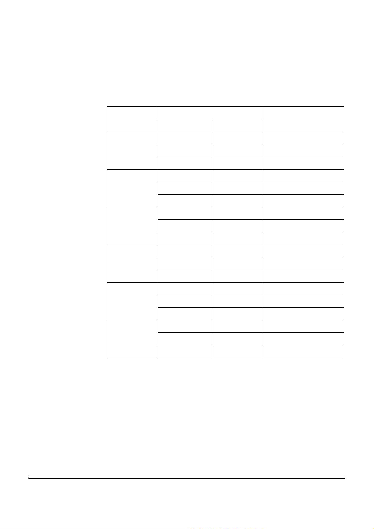
Table 1-1. Device Ordering Information
Package
112-Pin TQFP
Single Tray
60 Pcs
80-Pin TQFP
nc...
I
cale Semiconductor,
Single Tray
84 Pcs
112-Pin TQFP
Single Tray
60 Pcs
80-Pin TQFP
Single Tray
84 Pcs
112-Pin TQFP
Single Tray
60 Pcs
80-Pin TQFP
Single Tray
84 Pcs
Ambient Temperature
Order Number
Range Designator
–40 to +85°C C MC912D60ACPV8
–40 to +105°C V MC912D60AVPV8
–40 to +125°C M* MC912D60AMPV8
–40 to +85°C C MC912D60ACFU8
–40 to +105°C V MC912D60AVFU8
–40 to +125°C M* MC912D60AMFU8
–40 to +85°C C MC912D60CCPV8
–40 to +105°C V MC912D60CVPV8
–40 to +125°C M* MC912D60CMPV8
–40 to +85°C C MC912D60CCFU8
–40 to +105°C V MC912D60CVFU8
–40 to +125°C M* MC912D60CMFU8
–40 to +85°C C MC912D60PCPV8
–40 to +105°C V MC912D60PVPV8
–40 to +125°C M* MC912D60PMPV8
–40 to +85°C C MC912D60PCFU8
–40 to +105°C V MC912D60PVFU8
–40 to +125°C M* MC912D60PMFU8
Frees
* Important: M temperature operation is available only for single chip
modes
MC68HC912D60A — Rev 3.0 Technical Data
MOTOROLA General Description 27
For More Information On This Product,
Go to: www.freescale.com

General Description
Table 1-2. Development Tools Ordering Information
Description Name Order Number
MCUez Free from World Wide Web
Freescale Semiconductor, Inc.
Serial Debug Interface SDI
Evaluation board EVB
M68SDIL (3–5V), M68DIL12 (SDIL + MCUez +
SDBUG12)
M68EVB912D60 (EVB only)
M68KIT912D60 (EVB + SDIL12)
NOTE: SDBUG12 is a P & E Micro Product. It can be obtained from P & E from
nc...
I
cale Semiconductor,
their web site (http://www.pemicro.com) for approximately $100.
Third party tools: http://www.mcu.motsps.com/dev_tools/3rd/index.html
Frees
Technical Data MC68HC912D60A — Rev 3.0
28 General Description MOTOROLA
For More Information On This Product,
Go to: www.freescale.com
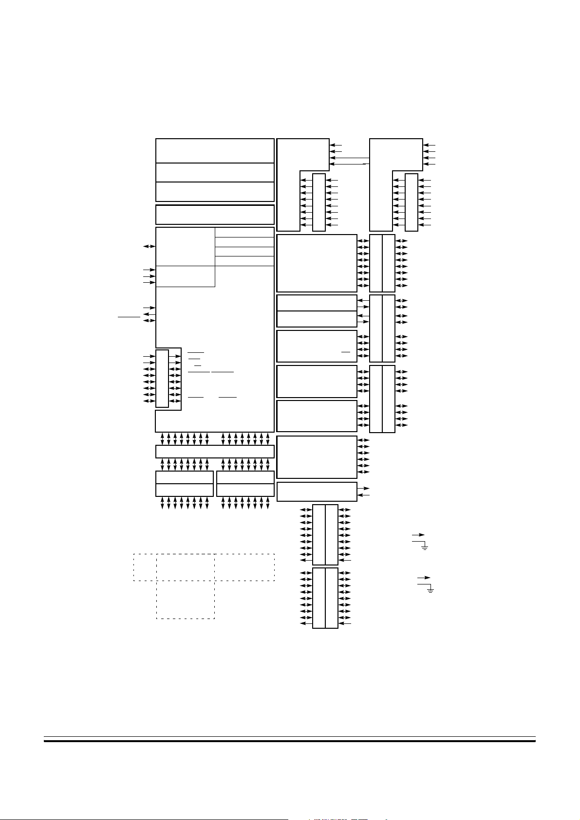
1.6 Block Diagrams
Freescale Semiconductor, Inc.
General Description
Block Diagrams
nc...
I
cale Semiconductor,
Frees
BKGD
XFC
VDDPLL
VSSPLL
EXTAL
XTAL
RESET
PE0
PE1
PE2
PE3
PE4
PE5
PE6
PE7
60K byte flash EEPROM
2K byte RAM
1K byte EEPROM
CPU12
Single-wire
background
debug module
PLL
integration
XIRQ
IRQ
R/W
LSTRB/TAGLO
ECLK
MODA/IPIPE0
PORT E
MODB/IPIPE1/CGMTST
DBE/CAL/ECLK
Multiplexed Address/Data Bus
DDRA
PORT A
PA 4
PA 3
PA 2
PA 1
PA 0
0
2
1
8
9
1
1
1
R
R
R
R
R
D
D
D
D
D
D
D
D
D
D
A
A
A
A
A
DATA9
DATA11
DATA12
DATA10
DATA4
DATA3
DATA2
DATA1
Wide
bus
PA 7
PA 6
PA 5
3
4
5
1
1
1
R
R
R
D
D
D
D
D
D
A
A
A
DATA14
DATA13
DATA15
DATA7
DATA6
DATA5
Narrow bus
Periodic interrupt
COP watchdog
Clock monitor
Breakpoints
Lite
module
(LIM)
DDRB
PORT B
PB4
PB3
PB7
PB6
PB5
2
5
4
3
7
6
R
R
R
R
R
R
D
D
D
D
D
D
D
D
D
D
D
D
A
A
A
A
A
A
DATA7
DATA6
DATA5
DATA4
DATA8
DATA0
DATA3
ATD0
SCI0 (MI BUS)
SCI1
KWG6
PB2
PB1
PB0
KWG5
1
0
KWG4
R
R
KWG3
D
D
KWG2
D
D
A
A
KWG1
KWG0
PGUPD
KWH7
DATA2
DATA1
DATA0
KWH6
KWH5
KWH4
KWH3
KWH2
KWH1
KWH0
PHUPD
VDDAD
VSSAD
AN00
AN01
AN02
AN03
AN04
AN05
AN06
AN07
Enhanced
capture
timer
SPI
PWM
PG7
VRH0
VRL0
PORT AD0
SISO/MISO
MOMI/MOSI
I/O
I/O
CAN
DDRG
DDRH
VRH0
VRL0
PAD00
PAD01
PAD02
PAD03
PAD04
PAD05
PAD06
PAD07
IOC0
IOC1
IOC2
IOC3
IOC4
IOC5
IOC6
IOC7
RxD0
TxD0
RxD1
TxD1
SCK
SS
PW0
PW1
PW2
PW3
PORTG
PORTH
PG7
PG6
PG5
PG4
PG3
PG2
PG1
PG0
PGUPD
PH7
PH6
PH5
PH4
PH3
PH2
PH1
PH0
PHUPD
VRH1
ATD1
VRL1
VDDAD
VSSAD
AN10
AN11
AN12
AN13
AN14
AN15
AN16
AN17
DDRT
DDRS
DDRP
PCAN7
PCAN6
PCAN5
PCAN4
PCAN3
PCAN2
TxCAN
RxCAN
VDD ×2
VSS ×2
PORT T
PORT S
PORT P
PCAN1
PCAN0
PAD10
PAD11
PAD12
PAD13
PAD14
PAD15
PAD16
PORT AD1
PAD17
PT0
PT1
PT2
PT3
PT4
PT5
PT6
PT7
PS0
PS1
PS2
PS3
PS4
PS5
PS6
PS7
PP0
PP1
PP2
PP3
PP4
PP5
PP6
PP7
Power for internal circuitry
VDDX ×2
VSSX ×2
Power for I/O drivers
VRH1
VRL1
VDDAD
VSSAD
Figure 1-1. MC68HC912D60A 112-pin QFP Block Diagram
MC68HC912D60A — Rev 3.0 Technical Data
MOTOROLA General Description 29
For More Information On This Product,
Go to: www.freescale.com
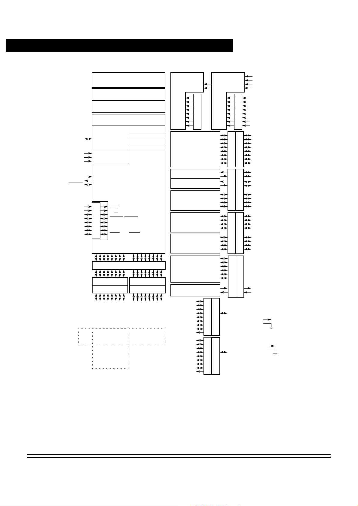
General Description
Freescale Semiconductor, Inc.
nc...
I
cale Semiconductor,
Frees
VRH1
ATD1
60K byte flash EEPROM
2K byte RAM
1K byte EEPROM
CPU12
Periodic interrupt
COP watchdog
Clock monitor
Breakpoints
Lite
integration
module
BKGD
XFC
VDDPLL
VSSPLL
EXTAL
XTAL
RESET
Single-wire
background
debug module
PLL
(LIM)
PE0
PE1
PE2
PE3
PE4
PE5
PE6
PE7
XIRQ
IRQ
R/W
LSTRB/TAGLO
ECLK
MODA/IPIPE0
PORT E
MODB/IPIPE1/CGMTST
DBE/CAL/ECLK
Multiplexed Address/Data Bus
Wide
bus
DDRA
PORT A
PA 4
PA 7
PA 6
PA 5
3
2
4
5
1
1
1
1
R
R
R
R
D
D
D
D
D
D
D
D
A
A
A
A
DATA14
DATA13
DATA12
DATA15
DATA7
DATA6
DATA5
DATA4
Narrow bus
PA 3
PA 2
PA 1
0
1
9
1
1
R
R
R
D
D
D
D
D
D
A
A
A
DATA9
DATA11
DATA10
DATA3
DATA2
DATA1
DDRB
PORT B
PA 0
8
R
D
D
A
DATA8
DATA0
PB4
PB3
PB2
PB1
PB7
PB6
PB5
6
5
7
R
R
R
D
D
D
D
D
D
A
A
A
DATA7
DATA6
DATA5
PB0
0
3
2
1
4
R
R
R
R
R
D
D
D
D
D
D
D
D
D
D
A
A
A
A
A
PGUPD(VDD)
DATA4
DATA3
DATA2
DATA1
DATA0
PHUPD(VSS)
VRL1
VDDAD
VSSAD
AN10
AN11
AN12
AN13
AN14
AN15
AN16
AN17
PORT AD1
Enhanced
capture
timer
SCI0 (MI BUS)
SCI1
SISO/MISO
SPI
MOMI/MOSI
PWM
I/O
CAN
PG7
KWG6
KWG5
KWG4
KWG3
KWG2
KWG1
KWG0
KWH7
KWH6
KWH5
KWH4
KWH3
KWH2
KWH1
KWH0
IOC0
IOC1
IOC2
IOC3
IOC4
IOC5
IOC6
IOC7
RxD0
TxD0
RxD1
TxD1
SCK
SS
PW0
PW1
PW2
PW3
PCAN7
PCAN6
PCAN5
PCAN4
PCAN3
PCAN2
DDRG
DDRH
ATD0
AN00
AN01
AN02
AN03
AN04
AN05
AN06
AN07
PORTG
PORTH
VRH0
VRL0
VDDAD
VSSAD
DDRT
DDRS
DDRP
DDRCAN
PG4
PH4
VRH0
VRL0
VDDAD
VSSAD
PAD00
PAD01
PAD02
PAD03
PAD04
PAD05
PAD06
PORT AD0
PAD07
PT0
PT1
PT2
PT3
PT4
PT5
PORT T
PT6
PT7
PS0
PS1
PS2
PS3
PS4
PORT S
PS5
PS6
PS7
PP0
PP1
PP2
PP3
PP4
PORT P
PP5
PP6
PP7
TxCAN
PORT CAN
VDD ×2
VSS ×2
RxCAN
PCAN1
PCAN0
Power for internal circuitry
VDDX ×2
VSSX ×2
Power for I/O drivers
Note:
Several I/O on ports G, H and CAN are unavailable externally on the 80-pin QFP package. These internal pins should either be defined as outputs or have their pull-ups/downs enabled.
Figure 1-2. MC68HC912D60A 80-pin QFP Block Diagram
Technical Data MC68HC912D60A — Rev 3.0
30 General Description MOTOROLA
For More Information On This Product,
Go to: www.freescale.com

Freescale Semiconductor, Inc.
Technical Data — MC68HC912D60A
Section 2. Central Processing Unit
2.1 Contents
2.2 Introduction . . . . . . . . . . . . . . . . . . . . . . . . . . . . . . . . . . . . . . . .31
2.3 Programming Model . . . . . . . . . . . . . . . . . . . . . . . . . . . . . . . . .31
nc...
I
2.2 Introduction
cale Semiconductor,
Frees
2.4 Data Types . . . . . . . . . . . . . . . . . . . . . . . . . . . . . . . . . . . . . . . .33
2.5 Addressing Modes . . . . . . . . . . . . . . . . . . . . . . . . . . . . . . . . . .33
2.6 Indexed Addressing Modes . . . . . . . . . . . . . . . . . . . . . . . . . . .35
2.7 Opcodes and Operands . . . . . . . . . . . . . . . . . . . . . . . . . . . . . .36
The CPU12 is a high-speed, 16-bit processing unit. It has full 16-bit data
paths and wider internal registers (up to 20 bits) for high-speed extended
math instructions. The instruction set is a proper superset of the
M68HC11instruction set. The CPU12 allows instructions with odd byte
counts, including many single-byte instructions. This provides efficient
use of ROM space. An instruction queue buffers program information so
the CPU always has immediate access to at least three bytes of machine
code at the start of every instruction. The CPU12 also offers an
extensive set of indexed addressing capabilities.
2.3 Programming Model
CPU12 registers are an integral part of the CPU and are not addressed
as if they were memory locations.
MC68HC912D60A — Rev 3.0 Technical Data
MOTOROLA Central Processing Unit 31
For More Information On This Product,
Go to: www.freescale.com

D
Freescale Semiconductor, Inc.
Central Processing Unit
7
15
15
15
15
nc...
I
15
AB
D
IX
IY
SP
PC
70
NSXH I ZVC
8-BIT ACCUMULATORS A & B
0
OR
16-BIT DOUBLE ACCUMULATOR
0
0
INDEX REGISTER X
0
INDEX REGISTER Y
0
STACK POINTER
0
PROGRAM COUNTER
CONDITION CODE REGISTER
Figure 2-1. Programming Model
Accumulators A and B are general-purpose 8-bit accumulators used to
hold operands and results of arithmetic calculations or data
manipulations. Some instructions treat the combination of these two 8bit accumulators as a 16-bit double accumulator (accumulator D).
Index registers X and Y are used for indexed addressing mode. In the
cale Semiconductor,
indexed addressing mode, the contents of a 16-bit index register are
added to 5-bit, 9-bit, or 16-bit constants or the content of an accumulator
to form the effective address of the operand to be used in the instruction.
Frees
Stack pointer (SP) points to the last stack location used. The CPU12
supports an automatic program stack that is used to save system
context during subroutine calls and interrupts, and can also be used for
temporary storage of data. The stack pointer can also be used in all
indexed addressing modes.
Program counter is a 16-bit register that holds the address of the next
instruction to be executed. The program counter can be used in all
indexed addressing modes except autoincrement/decrement.
Technical Data MC68HC912D60A — Rev 3.0
32 Central Processing Unit MOTOROLA
For More Information On This Product,
Go to: www.freescale.com

nc...
I
2.4 Data Types
Freescale Semiconductor, Inc.
Condition Code Register (CCR) contains five status indicators, two
interrupt masking bits, and a STOP disable bit. The five flags are half
carry (H), negative (N), zero (Z), overflow (V), and carry/borrow (C). The
half-carry flag is used only for BCD arithmetic operations. The N, Z, V,
and C status bits allow for branching based on the results of a previous
operation.
After a reset, the CPU fetches a vector from the appropriate address and
begins executing instructions. The X and I interrupt mask bits are set to
mask any interrupt requests. The S bit is also set to inhibit the STOP
instruction.
Central Processing Unit
Data Types
cale Semiconductor,
2.5 Addressing Modes
Frees
The CPU12 supports the following data types:
• Bit data
• 8-bit and 16-bit signed and unsigned integers
• 16-bit unsigned fractions
• 16-bit addresses
A byte is eight bits wide and can be accessed at any byte location. A
word is composed of two consecutive bytes with the most significant
byte at the lower value address. There are no special requirements for
alignment of instructions or operands.
Addressing modes determine how the CPU accesses memory locations
to be operated upon. The CPU12 includes all of the addressing modes
of the M68HC11 CPU as well as several new forms of indexed
addressing. Table 2-1 is a summary of the available addressing modes.
MC68HC912D60A — Rev 3.0 Technical Data
MOTOROLA Central Processing Unit 33
For More Information On This Product,
Go to: www.freescale.com

Freescale Semiconductor, Inc.
Central Processing Unit
Table 2-1. M68HC12 Addressing Mode Summary
Addressing Mode Source Format Abbreviation Description
INST
Inherent
(no externally
supplied operands)
INH Operands (if any) are in CPU registers
nc...
I
cale Semiconductor,
Frees
Immediate
Direct INST opr8a DIR
Extended INST opr16a EXT Operand is a 16-bit address
Relative
Indexed
(5-bit offset)
(auto post-decrement)
Indexed
(auto pre-decrement)
Indexed
(auto pre-increment)
Indexed
Indexed
(auto post-increment)
Indexed
(accumulator offset)
Indexed
(9-bit offset)
INST #opr8i
or
INST #opr16i
INST rel8
or
INST rel16
INST oprx5,xysp IDX
INST oprx3,–xys IDX Auto pre-decrement x, y, or sp by 1 ~ 8
INST oprx3,+xys IDX Auto pre-increment x, y, or sp by 1 ~ 8
INST oprx3,xys– IDX Auto post-decrement x, y, or sp by 1 ~ 8
INST oprx3,xys+ IDX Auto post-increment x, y, or sp by 1 ~ 8
INST abd,xysp IDX
INST oprx9,xysp IDX1
IMM
REL
Operand is included in instruction stream
8- or 16-bit size implied by context
Operand is the lower 8-bits of an address in
the range $0000 – $00FF
An 8-bit or 16-bit relative offset from the
current pc is supplied in the instruction
5-bit signed constant offset from x, y, sp, or
pc
Indexed with 8-bit (A or B) or 16-bit (D)
accumulator offset from x, y, sp, or pc
9-bit signed constant offset from x, y, sp, or
pc
(lower 8-bits of offset in one extension byte)
Indexed
(16-bit offset)
Indexed-Indirect
(16-bit offset)
Indexed-Indirect
(D accumulator offset)
Technical Data MC68HC912D60A — Rev 3.0
34 Central Processing Unit MOTOROLA
INST oprx16,xysp IDX2
INST [oprx16,xysp] [IDX2]
INST [D,xysp] [D,IDX]
For More Information On This Product,
Go to: www.freescale.com
16-bit constant offset from x, y, sp, or pc
(16-bit offset in two extension bytes)
Pointer to operand is found at...
16-bit constant offset from x, y, sp, or pc
(16-bit offset in two extension bytes)
Pointer to operand is found at...
x, y, sp, or pc plus the value in D

Freescale Semiconductor, Inc.
2.6 Indexed Addressing Modes
The CPU12 indexed modes reduce execution time and eliminate code
size penalties for using the Y index register. CPU12 indexed addressing
uses a postbyte plus zero, one, or two extension bytes after the
instruction opcode. The postbyte and extensions do the following tasks:
• Specify which index register is used.
• Determine whether a value in an accumulator is used as an offset.
• Enable automatic pre- or post-increment or decrement
• Specify use of 5-bit, 9-bit, or 16-bit signed offsets.
nc...
I
Central Processing Unit
Indexed Addressing Modes
cale Semiconductor,
Frees
Postbyte
Code (xb)
rr0nnnnn
111rr0zs
111rr011 [n,r]
rr1pnnnn
111rr1aa
Source
Syntax
,r
n,r
–n,r
n,r
–n,r
n,–r n,+r
n,r– n,r+
A,r
B,r
D,r
Table 2-2. Summary of Indexed Operations
Code
5-bit constant offset n = –16 to +15
rr can specify X, Y, SP, or PC
Constant offset (9- or 16-bit signed)
z-0 = 9-bit with sign in LSB of postbyte(s)
1 = 16-bit
if z = s = 1, 16-bit offset indexed-indirect (see below)
rr can specify X, Y, SP, or PC
16-bit offset indexed-indirect
rr can specify X, Y, SP, or PC
Auto pre-decrement/increment or Auto post-
decrement/increment;
p = pre-(0) or post-(1), n = –8 to –1, +1 to +8
rr can specify X, Y, or SP (PC not a valid choice)
Accumulator offset (unsigned 8-bit or 16-bit)
aa-00 = A
01 = B
10 = D (16-bit)
11 = see accumulator D offset indexed-indirect
rr can specify X, Y, SP, or PC
Comments
111rr111 [D,r]
MC68HC912D60A — Rev 3.0 Technical Data
MOTOROLA Central Processing Unit 35
For More Information On This Product,
Accumulator D offset indexed-indirect
rr can specify X, Y, SP, or PC
Go to: www.freescale.com

Freescale Semiconductor, Inc.
Central Processing Unit
2.7 Opcodes and Operands
The CPU12 uses 8-bit opcodes. Each opcode identifies a particular
instruction and associated addressing mode to the CPU. Several
opcodes are required to provide each instruction with a range of
addressing capabilities.
Only 256 opcodes would be available if the range of values were
restricted to the number that can be represented by 8-bit binary
numbers. To expand the number of opcodes, a second page is added to
the opcode map. Opcodes on the second page are preceded by an
additional byte with the value $18.
nc...
I
cale Semiconductor,
Frees
To provide additional addressing flexibility, opcodes can also be
followed by a postbyte or extension bytes. Postbytes implement certain
forms of indexed addressing, transfers, exchanges, and loop primitives.
Extension bytes contain additional program information such as
addresses, offsets, and immediate data.
Technical Data MC68HC912D60A — Rev 3.0
36 Central Processing Unit MOTOROLA
For More Information On This Product,
Go to: www.freescale.com

Freescale Semiconductor, Inc.
Technical Data — MC68HC912D60A
Section 3. Pinout and Signal Descriptions
3.1 Contents
3.2 MC68HC912D60A Pin Assignments in 112-pin QFP . . . . . . . .38
3.3 MC68HC912D60A Pin Assignments in 80-pin QFP . . . . . . . . .40
nc...
I
cale Semiconductor,
Frees
3.4 Power Supply Pins . . . . . . . . . . . . . . . . . . . . . . . . . . . . . . . . . .42
3.5 Signal Descriptions . . . . . . . . . . . . . . . . . . . . . . . . . . . . . . . . . .44
3.6 Port Signals . . . . . . . . . . . . . . . . . . . . . . . . . . . . . . . . . . . . . . .52
MC68HC912D60A — Rev 3.0 Technical Data
MOTOROLA Pinout and Signal Descriptions 37
For More Information On This Product,
Go to: www.freescale.com

Freescale Semiconductor, Inc.
Pinout and Signal Descriptions
3.2 MC68HC912D60A Pin Assignments in 112-pin QFP
nc...
I
cale Semiconductor,
Frees
PW2/PP2
PW1/PP1
PW0/PP0
IOC0/PT0
IOC1/PT1
IOC2/PT2
IOC3/PT3
KWG6/PG6
KWG5/PG5
KWG4/PG4
IOC4/PT4
IOC5/PT5
IOC6/PT6
IOC7/PT7
KWG3/PG3
KWG2/PG2
KWG1/PG1
KWG0/PG0
SMODN/TAGHI
ADDR0/DATA0/PB0
ADDR1/DATA1/PB1
ADDR2/DATA2/PB2
ADDR3/DATA3/PB3
ADDR4/DATA4/PB4
PG7
V
PGUPD
V
/BKGD
PP3/PW3
PP4
PP5
112
111
1
2
3
4
5
6
7
8
9
10
11
12
DD
13
14
SS
15
16
17
18
19
20
21
22
23
24
25
26
27
28
110
293031323334353637383940414243444546474849505152535455
ADDR6/DATA6/PB6
ADDR7/DATA7/PB7
ADDR5/DATA5/PB5
DDXVSSX
PP6
PP7
V
109
108
107
KWH7/PH7
KWH6/PH6
KWH5/PH5
PCAN0/RxCAN
PCAN1/TxCAN
106
105
104
KWH4/PH4
/DBE/CAL/PE7
ECLK
PCAN2
PCAN3
PCAN4
PCAN5
PCAN6
PCAN7
TEST
PS7/SS
103
999897969594939291908988878685
102
101
100
MC68HC912D60A
112TQFP
SSX
DDX
PHUPD
XFC
V
DDPLL
V
V
V
ECLK/PE4
MODA/IPIPE0/PE5
PS6/SCK
SSPLL
RESET
PS5/SDO/MOSI
EXTAL
PS4/SDI/MISO
PS3/TxD1
XTAL
KWH3/PH3
PS2/RxD1
KWH2/PH2
SSAVRL1VRH1VDDA
PS1/TxD0
PS0/RxD0
V
KWH1/PH1
KWH0/PH0
/TAGLO/PE3
LSTRB
/PE2
R/W
/PE1
IRQ
PAD17/AN17
84
PAD07/AN07
83
PAD16/AN16
82
PAD06/AN06
81
PAD15/AN15
80
PAD05/AN05
79
PAD14/AN14
78
PAD04/AN04
77
PAD13/AN13
76
PAD03/AN03
75
PAD12/AN12
74
PAD02/AN02
73
PAD11/AN11
72
PAD01/AN01
71
PAD10/AN10
70
PAD00/AN00
69
V
68
RL0
V
67
RH0
V
66
SS
V
65
DD
PA7/ADDR15/DATA15/DATA7
64
PA6/ADDR14/DATA14/DATA6
63
PA5/ADDR13/DATA13/DATA5
62
PA4/ADDR12/DATA12/DATA4
61
PA3/ADDR11/DATA11/DATA3
60
PA2/ADDR10/DATA10/DATA2
59
PA1/ADDR9/DATA9/DATA1
58
PA0/ADDR8/DATA8/DATA0
57
56
/PE0
XIRQ
CGMTST/MODB/IPIPE1/PE6
Note: TEST =
This pin is used for factory test purposes. It is recommended that this pin is not connected in the
application, but it may be bonded to 5.5 V max without issue.
Never apply voltage higher than 5.5 V to this pin.
Figure 3-1. Pin Assignments in 112-pin TQFP for MC68HC912D60A
Technical Data MC68HC912D60A — Rev 3.0
38 Pinout and Signal Descriptions MOTOROLA
For More Information On This Product,
Go to: www.freescale.com

Freescale Semiconductor, Inc.
MC68HC912D60A Pin Assignments in 112-pin QFP
Pinout and Signal Descriptions
nc...
I
cale Semiconductor,
Frees
PIN 1
IDENT
C
4X
112 85
1
L
28 57
29 56
C2
C1
VIEW Y
S1
0.050
VIEW AB
A1
T
L-M0.20 N
4X 28 TIPS
N
A
S
2θ
3
θ
θ
R
R2
R1
R
(K)
E
(Y)
(Z)
L-M0.20 NT
84
V
B
M
B1
V1
VIEW AB
T
SEATING
PLANE
112X
0.10
T
0.25
GAGE PLANE
1θ
J1
J1
C
L
J
0.13 NT
SECTION J1-J1
ROTATED 90 COUNTERCLOCKWISE
NOTES:
1. DIMENSIONING AND TOLERANCING PER
ASME Y14.5M, 1994.
2. DIMENSIONS IN MILLIMETERS.
3. DATUMS L, M AND N TO BE DETERMINED AT
SEATING PLANE, DATUM T.
4. DIMENSIONS S AND V TO BE DETERMINED AT
SEATING PLANE, DATUM T.
5. DIMENSIONS A AND B DO NOT INCLUDE
MOLD PROTRUSION. ALLOWABLE
PROTRUSION IS 0.25 PER SIDE. DIMENSIONS
A AND B INCLUDE MOLD MISMATCH.
6. DIMENSION D DOES NOT INCLUDE DAMBAR
PROTRUSION. ALLOWABLE DAMBAR
PROTRUSION SHALL NOT CAUSE THE D
DIMENSION TO EXCEED 0.46.
DIMAMIN MAX
A1 10.000 BSC
B 20.000 BSC
B1 10.000 BSC
C --- 1.600
C1 0.050 0.150
C2 1.350 1.450
D 0.270 0.370
E 0.450 0.750
F 0.270 0.330
G 0.650 BSC
J 0.090 0.170
K 0.500 REF
P 0.325 BSC
R1 0.100 0.200
R2 0.100 0.200
S 22.000 BSC
S1 11.000 BSC
V 22.000 BSC
V1 11.000 BSC
Y 0.250 REF
Z 1.000 REF
AA 0.090 0.160
θ
θ
1
θ
2
θ
3
108X
G
VIEW Y
F
D
M
°
MILLIMETERS
20.000 BSC
0 °
3 °
11 °
11 °
4X
P
X
X=L, M OR N
L-M
8 °
7 °
13 °
13 °
AA
BASE
METAL
Figure 3-2. 112-pin TQFP Mechanical Dimensions (case no. 987)
MC68HC912D60A — Rev 3.0 Technical Data
MOTOROLA Pinout and Signal Descriptions 39
For More Information On This Product,
Go to: www.freescale.com

Freescale Semiconductor, Inc.
Pinout and Signal Descriptions
3.3 MC68HC912D60A Pin Assignments in 80-pin QFP
nc...
I
cale Semiconductor,
Frees
PP3/PW3
PP4
PP5
80
79
PW2/PP2
PW1/PP1
PW0/PP0
IOC0/PT0
IOC1/PT1
IOC2/PT2
IOC3/PT3
KWG4/PG4
V
IOC4/PT4
IOC5/PT5
SMODN/TAGHI/
ADDR0/DATA0/PB0
ADDR1/DATA1/PB1
ADDR2/DATA2/PB2
ADDR3/DATA3/PB3
ADDR4/DATA4/PB4
IOC6/PT6
IOC7/PT7
BKGD
1
2
3
4
5
6
7
8
9
DD
10
V
SS
11
12
13
14
15
16
17
18
19
20
21
22
ADDR5/DATA5/PB5
ADDR6/DATA6/PB6
ADDR7/DATA7/PB7
DDXVSSX
PP6
PP7
V
PCAN0/RxCAN
PCAN1/TxCAN
TEST
PS7/SS
PS6/SCK
PS5/SDO/MOSI
PS4/SDI/MISO
PS3/TxD1
PS2/RxD1
7776757473727170696867666578646362
MC68HC912D60A
80 QFP
2425262728293031323334353623384039
SSX
DDX
V
KWH4/PH4
/DBE/CAL/PE7
ECLK
ECLK/PE4
MODA/IPIPE0/PE5
CGMTST/MODB/IPIPE1/PE6
XFC
V
SSPLL
DDPLL
V
V
EXTAL
RESET
XTAL
PS1/TxD0
PS0/RxD0
37
/PE2
R/W
/TAGLO/PE3
LSTRB
SSADVDDAD
V
/PE1
IRQ
61
60
PAD07/AN07
59
PAD06/AN06
58
PAD05/AN05
57
PAD04/AN04
56
PAD03/AN03
55
PAD02/AN02
54
PAD01/AN01
53
PAD00/AN00
52
V
RL0
51
V
RH0
50
V
SS
49
V
DD
48
PA7/ADDR15/DATA15/DATA7
47
PA6/ADDR14/DATA14/DATA6
46
PA5/ADDR13/DATA13/DATA5
45
PA4/ADDR12/DATA12/DATA4
44
PA3/ADDR11/DATA11/DATA3
43
PA2/ADDR10/DATA10/DATA2
42
PA1/ADDR9/DATA9/DATA1
41
PA0/ADDR8/DATA8/DATA0
/PE0
XIRQ
Note: TEST =
This pin is used for factory test purposes. It is recommended that this pin is not connected in the
application, but it may be bonded to 5.5 V max without issue.
Never apply voltage higher than 5.5 V to this pin.
Figure 3-3. Pin Assignments in 80-pin QFP for MC68HC912D60A
Technical Data MC68HC912D60A — Rev 3.0
40 Pinout and Signal Descriptions MOTOROLA
For More Information On This Product,
Go to: www.freescale.com

Freescale Semiconductor, Inc.
MC68HC912D60A Pin Assignments in 80-pin QFP
L
Pinout and Signal Descriptions
nc...
I
cale Semiconductor,
Frees
60
61
-A-
L
DETAIL A
80
120
M
0.20 D
0.05
A-B
M
0.20 D
E
C DATUM
-C-
SEATING
PLANE
DATUM
PLANE
H
G
-H-
W
X
DETAIL C
-D-
A
S
A-B
H
S
A-B
C
K
S
S
S
U
T
R
Q
41
40
-B-
21
M
M
NOTES:
1. DIMENSIONING AND TOLERANCING PER
ANSI Y14.5M, 1982.
2. CONTROLLING DIMENSION: MILLIMETER.
3. DATUM PLANE -H- IS LOCATED AT BOTTOM OF
LEAD AND IS COINCIDENT WITH THE
LEAD WHERE THE LEAD EXITS THE PLASTIC
BODY AT THE BOTTOM OF THE PARTING LINE.
4. DATUMS -A-, -B- AND -D- TO BE
DETERMINED AT DATUM PLANE -H-.
5. DIMENSIONS S AND V TO BE DETERMINED
AT SEATING PLANE -C-.
6. DIMENSIONS A AND B DO NOT INCLUDE
MOLD PROTRUSION. ALLOWABLE
PROTRUSION IS 0.25 PER SIDE. DIMENSIONS
A AND B DO INCLUDE MOLD MISMATCH
AND ARE DETERMINED AT DATUM PLANE -H-.
7. DIMENSION D DOES NOT INCLUDE DAMBAR
PROTRUSION. ALLOWABLE DAMBAR
PROTRUSION SHALL BE 0.08 TOTAL IN
S
S
A-B
B
H
M
0.20 D
DETAIL C
-H-
PLANE
0.10
S
S
A-B
V
C
D
M
0.20 D
0.05
B
B
DETAIL A
F
J
D
M
0.20 D
SECTION B-B
VIEW ROTATED 90
MILLIMETERS
DIM MIN MAX
A 13.90 14.10
B 13.90 14.10
C 2.15 2.45
D 0.22 0.38
E 2.00 2.40
F 0.22 0.33
G 0.65 BSC
H --- 0.25
J 0.13 0.23
K 0.65 0.95
L 12.35 REF
M 5 10
N 0.13 0.17
P 0.325 BSC
Q 0 7
R 0.13 0.30
S 16.95 17.45
T 0.13 ---
U 0 ---
V 16.95 17.45
W 0.35 0.45
X 1.6 REF
S
A-B
C
°
°°
°°
°
P
-A-,-B-,-D-
N
S
Figure 3-4. 80-pin QFP Mechanical Dimensions (case no. 841B)
MC68HC912D60A — Rev 3.0 Technical Data
MOTOROLA Pinout and Signal Descriptions 41
For More Information On This Product,
Go to: www.freescale.com

Freescale Semiconductor, Inc.
Pinout and Signal Descriptions
3.4 Power Supply Pins
MC68HC912D60A power and ground pins are described below and
summarized in Table 3-1.
All power supply pins must be connected to appropriate supplies.
On no account must any pins be left floating.
3.4.1 Internal Power (VDD) and Ground (VSS)
Power is supplied to the MCU through VDD and VSS. Because fast signal
transitions place high, short-duration current demands on the power
nc...
I
supply, use bypass capacitors with high-frequency characteristics and
place them as close to the MCU as possible. Bypass requirements
depend on how heavily the MCU pins are loaded.
3.4.2 External Power (V
External power and ground for I/O drivers. Because fast signal
and Ground (V
DDX)
transitions place high, short-duration current demands on the power
supply, use bypass capacitors with high-frequency characteristics and
place them as close to the MCU as possible. Bypass requirements
depend on how heavily the MCU pins are loaded.
cale Semiconductor,
3.4.3 V
DDA
, V
SSA
Provides operating voltage and ground for the analog-to-digital
converter. This allows the supply voltage to the ATD to be bypassed
Frees
independently. Connecting V
used will not result in an increase of power consumption.
3.4.4 Analog to Digital Reference Voltages (V
V
V
RH0
RH1
, V
, V
: reference voltage high and low for ATD converter 0.
RL0
: reference voltage high and low for ATD converter 1.
RL1
SSX
)
RH
to VDD if the ATD modules are not
DDA
, VRL)
If the ATD modules are not used, leaving V
connected to VDD will not
RH
result in an increase of power consumption.
Technical Data MC68HC912D60A — Rev 3.0
42 Pinout and Signal Descriptions MOTOROLA
For More Information On This Product,
Go to: www.freescale.com

Freescale Semiconductor, Inc.
Pinout and Signal Descriptions
Power Supply Pins
nc...
I
cale Semiconductor,
Frees
3.4.5 V
DDPLL
3.4.6 XFC
, V
SSPLL
Provides operating voltage and ground for the Phased-Locked Loop.
This allows the supply voltage to the PLL to be bypassed independently.
NOTE: The VSSPLL pin should always be grounded even if the PLL is not used.
The VDDPLL pin should not be left floating. It is recommended to
connect the VDDPLL pin to ground if the PLL is not used.
PLL loop filter. Please see Appendix: CGM Practical Aspects for
information on how to calculate PLL loop filter elements. Any current
leakage on this pin must be avoided.
VDDPLL
C
0
MCU
XFC
R
0
Figure 3-5. PLL Loop FIlter Connections
If VDDPLL is connected to VSS (this is normal case), then the XFC pin
should either be left floating or connected to VSS (never to VDD). If
VDDPLL is tied to VDD but the PLL is switched off (PLLON bit cleared),
then the XFC pin should be connected preferably to VDDPLL (i.e. ready
for VCO minimum frequency).
C
a
MC68HC912D60A — Rev 3.0 Technical Data
MOTOROLA Pinout and Signal Descriptions 43
For More Information On This Product,
Go to: www.freescale.com
Freescale Semiconductor, Inc.
Pinout and Signal Descriptions
Table 3-1. MC68HC912D60A Power and Ground Connection Summary
Pin Number
Mnemonic
80-pin
QFP
112-pin
QFP
Description
V
DD
V
SS
V
DDX
V
SSX
nc...
I
3.5 Signal Descriptions
cale Semiconductor,
V
DDA
V
V
V
V
V
V
DDPLL
V
SSPLL
SSA
RH1
RL1
RH0
RL0
9, 49 12, 65
10, 50 14, 66
30, 75 42, 107
29, 74 40, 106
61 85
62 88
—86
—87
51 67
52 68
31 43
33 45
Internal power and ground.
External power and ground, supply to pin drivers.
Operating voltage and ground for the analog-to-digital
converter, allows the supply voltage to the A/D to be
bypassed independently.
Reference voltages for the analog-to-digital converter 1
Reference voltages for the analog-to-digital converter 0.
Provides operating voltage and ground for the Phased-Locked
Loop. This allows the supply voltage to the PLL to be
bypassed independently.
3.5.1 Crystal Driver and External Clock Input (XTAL, EXTAL)
Frees
These pins provide the interface for either a crystal or a CMOS
compatible clock to control the internal clock generator circuitry. Out of
reset the frequency applied to EXTAL is twice the desired E–clock rate.
All the device clocks are derived from the EXTAL input frequency.
3.5.1.1 Crystal Connections
Refer to Section 12. Oscillator for details of crystal connections.
Technical Data MC68HC912D60A — Rev 3.0
44 Pinout and Signal Descriptions MOTOROLA
For More Information On This Product,
Go to: www.freescale.com

Freescale Semiconductor, Inc.
NOTE: When selecting a crystal, it is recommended to use one with the lowest
possible frequency in order to minimise EMC emissions.
3.5.1.2 External Oscillator Connections
XTAL is the crystal output. The XTAL pin must be left unterminated when
an external CMOS compatible clock input is connected to the EXTAL
pin. The XTAL output is normally intended to drive only a crystal. The
XTAL output can be buffered with a high-impedance buffer to drive the
EXTAL input of another device.
Pinout and Signal Descriptions
Signal Descriptions
nc...
I
3.5.2 E-Clock Output (ECLK)
cale Semiconductor,
Frees
2 x E
CMOS-COMPATIBLE
MCU
EXTAL
XTAL
EXTERNAL OSCILLATOR
NC
Figure 3-6. External Oscillator Connections
ECLK is the output connection for the internal bus clock and is used to
demultiplex the address and data and is used as a timing reference.
ECLK frequency is equal to 1/2 the crystal frequency out of reset. The
ECLK output is turned off in single chip user mode to reduce the effects
of RFI. It can be turned on if necessary. In single-chip special mode, the
ECLK is turned ON at reset and can be turned OFF. In special peripheral
mode the ECLK is an input to the MCU. All clocks, including the ECLK,
are halted when the MCU is in STOP mode. It is possible to configure
the MCU to interface to slow external memory. ECLK can be stretched
for such accesses.
3.5.3 Reset (RESET)
An active low bidirectional control signal, RESET, acts as an input to
initialize the MCU to a known start-up state. It also acts as an open-drain
MC68HC912D60A — Rev 3.0 Technical Data
MOTOROLA Pinout and Signal Descriptions 45
For More Information On This Product,
Go to: www.freescale.com

Pinout and Signal Descriptions
output to indicate that an internal failure has been detected in either the
clock monitor or COP watchdog circuit. The MCU goes into reset
asynchronously and comes out of reset synchronously. This allows the
part to reach a proper reset state even if the clocks have failed, while
allowing synchronized operation when starting out of reset.
It is important to use an external low-voltage reset circuit (such as
MC34064 or MC34164) to prevent corruption of RAM or EEPROM due
to power transitions.
The reset sequence is initiated by any of the following events:
nc...
I
Freescale Semiconductor, Inc.
• Power-on-reset (POR)
• COP watchdog enabled and watchdog timer times out
cale Semiconductor,
Frees
• Clock monitor enabled and Clock monitor detects slow or stopped
clock
• User applies a low level to the reset pin
External circuitry connected to the reset pin should not include a large
capacitance that would interfere with the ability of this signal to rise to a
valid logic one within nine bus cycles after the low drive is released.
Upon detection of any reset, an internal circuit drives the reset pin low
and a clocked reset sequence controls when the MCU can begin normal
processing. In the case of POR or a clock monitor error, a 4096 cycle
oscillator startup delay is imposed before the reset recovery sequence
starts (reset is driven low throughout this 4096 cycle delay). The internal
reset recovery sequence then drives reset low for 16 to 17 cycles and
releases the drive to allow reset to rise. Nine cycles later this circuit
samples the reset pin to see if it has risen to a logic one level. If reset is
low at this point, the reset is assumed to be coming from an external
request and the internally latched states of the COP timeout and clock
monitor failure are cleared so the normal reset vector ($FFFE:FFFF) is
taken when reset is finally released. If reset is high after this nine cycle
delay, the reset source is tentatively assumed to be either a COP failure
or a clock monitor fail. If the internally latched state of the clock monitor
fail circuit is true, processing begins by fetching the clock monitor vector
($FFFC:FFFD). If no clock monitor failure is indicated, and the latched
state of the COP timeout is true, processing begins by fetching the COP
Technical Data MC68HC912D60A — Rev 3.0
46 Pinout and Signal Descriptions MOTOROLA
For More Information On This Product,
Go to: www.freescale.com

Freescale Semiconductor, Inc.
vector ($FFFA:FFFB). If neither clock monitor fail nor COP timeout are
pending, processing begins by fetching the normal reset vector
($FFFE:FFFF).
3.5.4 Maskable Interrupt Request (IRQ)
The IRQ input provides a means of applying asynchronous interrupt
requests to the MCU. Either falling edge-sensitive triggering or levelsensitive triggering is program selectable (INTCR register). IRQ is
always enabled and configured to level-sensitive triggering at reset. It
can be disabled by clearing the IRQEN bit (INTCR register). When the
nc...
I
MCU is reset the IRQ function is masked in the condition code register.
This pin is always an input and can always be read. There is an active
pull-up on this pin while in reset and immediately out of reset. The pullup can be turned off by clearing PUPE in the PUCR register.
Pinout and Signal Descriptions
Signal Descriptions
3.5.5 Nonmaskable Interrupt (XIRQ)
The XIRQ input provides a means of requesting a nonmaskable interrupt
after reset initialization. During reset, the X bit in the condition code
register (CCR) is set and any interrupt is masked until MCU software
enables it. Because the XIRQ input is level sensitive, it can be connected
to a multiple-source wired-OR network. This pin is always an input and
can always be read. There is an active pull-up on this pin while in reset
cale Semiconductor,
Frees
and immediately out of reset. The pull-up can be turned off by clearing
PUPE in the PUCR register. XIRQ
interrupt.
Whenever XIRQ
must be configured for level-sensitive operation if there is more than one
source of IRQ interrupt), each source must drive the interrupt input with
an open-drain type of driver to avoid contention between outputs. There
must also be an interlock mechanism at each interrupt source so that the
source holds the interrupt line low until the MCU recognizes and
acknowledges the interrupt request. If the interrupt line is held low, the
MCU will recognize another interrupt as soon as the interrupt mask bit in
the MCU is cleared (normally upon return from an interrupt).
is often used as a power loss detect
or IRQ are used with multiple interrupt sources (IRQ
MC68HC912D60A — Rev 3.0 Technical Data
MOTOROLA Pinout and Signal Descriptions 47
For More Information On This Product,
Go to: www.freescale.com

Freescale Semiconductor, Inc.
Pinout and Signal Descriptions
3.5.6 Mode Select (SMODN, MODA, and MODB)
The state of these pins during reset determine the MCU operating mode.
After reset, MODA and MODB can be configured as instruction queue
tracking signals IPIPE0 and IPIPE1. MODA and MODB have active pulldowns during reset.
The SMODN pin has an active pull-up when configured as input. This pin
can be used as BKGD or TAGHI after reset.
3.5.7 Single-Wire Background Mode Pin (BKGD)
nc...
I
3.5.8 External Address and Data Buses (ADDR[15:0] and DATA[15:0])
The BKGD pin receives and transmits serial background debugging
commands. A special self-timing protocol is used. The BKGD pin has an
active pull-up when configured as input; BKGD has no pull-up control.
Refer to Development Support.
External bus pins share function with general-purpose I/O ports A and B.
In single-chip operating modes, the pins can be used for I/O; in
expanded modes, the pins are used for the external buses.
In expanded wide mode, ports A and B are used for multiplexed 16-bit
data and address buses. PA[7:0] correspond to
ADDR[15:8]/DATA[15:8]; PB[7:0] correspond to ADDR[7:0]/DATA[7:0].
cale Semiconductor,
In expanded narrow mode, ports A and B are used for the16-bit address
bus, and an 8-bit data bus is multiplexed with the most significant half of
Frees
the address bus on port A. In this mode, 16-bit data is handled as two
back-to-back bus cycles, one for the high byte followed by one for the
low byte. PA[7:0] correspond to ADDR[15:8] and to DATA[15:8] or
DATA[7:0], depending on the bus cycle. The state of the address pin
should be latched at the rising edge of E. To allow for maximum address
setup time at external devices, a transparent latch should be used.
Technical Data MC68HC912D60A — Rev 3.0
48 Pinout and Signal Descriptions MOTOROLA
For More Information On This Product,
Go to: www.freescale.com

3.5.9 Read/Write (R/W)
3.5.10 Low-Byte Strobe (LSTRB)
nc...
I
Freescale Semiconductor, Inc.
In all modes this pin can be used as general-purpose I/O and is an input
with an active pull-up out of reset. If the read/write function is required it
should be enabled by setting the RDWE bit in the PEAR register.
External writes will not be possible until enabled.
In all modes this pin can be used as general-purpose I/O and is an input
with an active pull-up out of reset. If the strobe function is required, it
should be enabled by setting the LSTRE bit in the PEAR register. This
signal is used in write operations and so external low byte writes will not
be possible until this function is enabled. This pin is also used as TAGLO
in Special Expanded modes and is multiplexed with the LSTRB function.
Pinout and Signal Descriptions
Signal Descriptions
3.5.11 Instruction Queue Tracking Signals (IPIPE1 and IPIPE0)
These signals are used to track the state of the internal instruction
execution queue. Execution state is time-multiplexed on the two signals.
Refer to Development Support.
3.5.12 Data Bus Enable (DBE)
cale Semiconductor,
Frees
The DBE
ECLK high time. DBE
multiplexed address and the input of data. When an external address is
stretched, DBE
of the last ECLK cycle of stretch. In expanded modes this pin is used to
enable the drive control of external buses during external reads. Use of
the DBE is controlled by the NDBE bit in the PEAR register.DBE is
enabled out of reset in expanded modes. This pin has an active pull-up
during and after reset in single chip modes.
pin (PE7) is an active low signal that will be asserted low during
provides separation between output of a
is asserted during what would be the last quarter cycle
MC68HC912D60A — Rev 3.0 Technical Data
MOTOROLA Pinout and Signal Descriptions 49
For More Information On This Product,
Go to: www.freescale.com

Pinout and Signal Descriptions
3.5.13 Inverted ECLK (ECLK)
The ECLK pin (PE7) can be used to latch the address for demultiplexing. It has the same behavior as the ECLK, except is inverted.
In expanded modes this pin is used to enable the drive control of external
buses during external reads. Use of the ECLK is controlled by the NDBE
and DBENE bits in the PEAR register.
3.5.14 Calibration reference (CAL)
The CAL pin (PE7) is the output of the Slow Mode programmable clock
divider, SLWCLK, and is used as a calibration reference. The SLWCLK
nc...
I
frequency is equal to the crystal frequency out of reset and always has
a 50% duty. If the DBE function is enabled it will override the enabled
CAL output. The CAL pin output is disabled by clearing CALE bit in the
PEAR register.
Freescale Semiconductor, Inc.
3.5.15 Clock generation module test (CGMTST)
The CGMTST pin (PE6) is the output of the clocks tested when CGMTE
bit is set in PEAR register. The PIPOE bit must be cleared for the clocks
to be tested.
3.5.16 TEST
cale Semiconductor,
This pin is used for factory test purposes. It is recommended that this
pin is not connected in the application, but it may be bonded to 5.5 V max
without issue. Never apply voltage higher than 5.5 V to this pin.
Frees
Table 3-2. MC68HC912D60A Signal Description Summary
Pin Name
EXTAL 35 47
XTAL 36 48
RESET
Pin Number
80-pin 112-pin
34 46
Crystal driver and external clock input pins.
An active low bidirectional control signal, RESET
initialize the MCU to a known start-up state, and an output when COP or
clock monitor causes a reset.
Description
acts as an input to
Technical Data MC68HC912D60A — Rev 3.0
50 Pinout and Signal Descriptions MOTOROLA
For More Information On This Product,
Go to: www.freescale.com

Freescale Semiconductor, Inc.
Pinout and Signal Descriptions
Table 3-2. MC68HC912D60A Signal Description Summary
Signal Descriptions
nc...
I
cale Semiconductor,
Frees
Pin Name
ADDR[7:0]
DATA[7:0]
ADDR[15:8]
DATA[15:8]
DBE
ECLK
CAL 25 36
CGMTST 26 37 Clock generation module test output.
MODB/
IPIPE1,
MODA/
IPIPE0
ECLK 28 39
LSTRB
TAG L O
/
R/W
IRQ
XIRQ
Pin Number
80-pin 112-pin
23–16 31–24
48–41 64–57
25 36
25 36 Inverted ECLK used to latch the address.
26, 27 37, 38
37 53
38 54
39 55
40 56
External bus pins share function with general-purpose I/O ports A and B.
In single chip modes, the pins can be used for I/O. In expanded modes,
the pins are used for the external buses.
Data bus control and, in expanded mode, enables the drive control of
external buses during external reads.
CAL is the output of the Slow Mode programmable clock divider, SLWCLK,
and is used as a calibration reference for functions such as time of day. It
is overridden when DBE function is enabled. It always has a 50% duty
cycle.
State of mode select pins during reset determine the initial operating mode
of the MCU. After reset, MODB and MODA can be configured as
instruction queue tracking signals IPIPE1 and IPIPE0 or as generalpurpose I/O pins.
E Clock is the output connection for the external bus clock. ECLK is used
as a timing reference and for address demultiplexing.
Low byte strobe (0 = low byte valid), in all modes this pin can be used as
I/O. The low strobe function is the exclusive-NOR of A0 and the internal
SZ8
signal. (The SZ8 internal signal indicates the size 16/8 access.) Pin
function TAGLO
Indicates direction of data on expansion bus. Shares function with
general-purpose I/O. Read/write in expanded modes.
Maskable interrupt request input provides a means of applying
asynchronous interrupt requests to the MCU. Either falling edgesensitive triggering or level-sensitive triggering is program selectable
(INTCR register).
Provides a means of requesting asynchronous nonmaskable interrupt
requests after reset initialization
used in instruction tagging. See Development Support.
Description
Single-wire background interface pin is dedicated to the background
SMODN/BK
GD/TAGHI
PW[3:0] 80, 1–3 112, 1–3 Pulse Width Modulator channel outputs.
SS
SCK 69 95 Serial clock for SPI system.
MC68HC912D60A — Rev 3.0 Technical Data
MOTOROLA Pinout and Signal Descriptions 51
15 23
70 96
debug function. During reset, this pin determines special or normal
operating mode. Pin function TAGHI
Development Support.
Slave select output for SPI master mode, input for slave mode or master
mode.
used in instruction tagging. See
For More Information On This Product,
Go to: www.freescale.com

Freescale Semiconductor, Inc.
Pinout and Signal Descriptions
Table 3-2. MC68HC912D60A Signal Description Summary
Pin Name
SDO/MOSI 68 94 Master out/slave in pin for serial peripheral interface
SDI/MISO 67 93 Master in/slave out pin for serial peripheral interface
TxD1 66 92 SCI1 transmit pin
RxD1 65 91 SCI1 receive pin
TxD0 64 90 SCI0 transmit pin
RxD0 63 89 SCI0 receive pin
IOC[7:0]
nc...
I
cale Semiconductor,
AN1[7:0] N/A
AN0[7:0] 60–53
TEST 71 97
TxCAN 72 104 MSCAN transmit pin. Leave unconnected if MSCAN is not used.
RxCAN 73 105
KWG[6:0]
PGUPD
KWH[7:0]
PHUPD
Pin Number
80-pin 112-pin
14–11,
7–4
8 (KWG4
only)
(1)
24 (KWH4
only)
(2)
18–15, 7–4
84/82/80/78/
76/74/72/70
83/81/79/77/
75/73/71/69
9–11, 19–22
32–35,
49–52
Description
Pins used for input capture and output compare in the timer and pulse
accumulator subsystem.
Analog inputs for the analog-to-digital conversion module 1
Analog inputs for the analog-to-digital conversion module 0
Used for factory test purposes. Do not connect in the application; may be
bonded to 5.5 V max.
MSCAN receive pin. Pin has internal pull-up; where msCAN module is not
used, do not tie to VSS.
Key wake-up and general purpose I/O; can cause an interrupt when an
input transitions from high to low. On 80-pin QFP all 8 I/O should be
initialised.
13 Defines if I/O port resistive load is a pull-up or a pull-down, when enabled.
Key wake-up and general purpose I/O; can cause an interrupt when an
input transitions from high to low. On 80-pin QFP all 8 I/O should be
initialised.
41 Defines if I/O port resistive load is a pull-up or a pull-down, when enabled.
Frees
1. In the 80-pin version PGUPD is connected internally to VDD
2. In the 80-pin version PHUPD is connected internally to VSS
3.6 Port Signals
The MC68HC912D60A incorporates eight ports which are used to
control and access the various device subsystems. When not used for
these purposes, port pins may be used for general-purpose I/O. In
addition to the pins described below, each port consists of a data register
Technical Data MC68HC912D60A — Rev 3.0
52 Pinout and Signal Descriptions MOTOROLA
For More Information On This Product,
Go to: www.freescale.com

3.6.1 Port A
Freescale Semiconductor, Inc.
which can be read and written at any time, and, with the exception of port
AD0, port AD1 (available only in 112TQFP), PE[1:0], RxCAN and
TxCAN, a data direction register which controls the direction of each pin.
After reset all general purpose I/O pins are configured as input.
Port A pins are used for address and data in expanded modes. In single
chip modes, the pins can be used as I/O. The port data register is not in
the address map during expanded and peripheral mode operation.
When it is in the map, port A can be read or written at anytime.
Pinout and Signal Descriptions
Port Signals
nc...
I
cale Semiconductor,
3.6.2 Port B
Frees
Register DDRA determines whether each port A pin is an input or output.
DDRA is not in the address map during expanded and peripheral mode
operation. Setting a bit in DDRA makes the corresponding bit in port A
an output; clearing a bit in DDRA makes the corresponding bit in port A
an input. The default reset state of DDRA is all zeros.
When the PUPA bit in the PUCR register is set, all port A input pins are
pulled-up internally by an active pull-up device. This bit has no effect if
the port is being used in expanded modes as the pull-ups are inactive.
Setting the RDPA bit in register RDRIV causes all port A outputs to have
reduced drive level. RDRIV can be written once after reset. RDRIV is not
in the address map in peripheral mode. Refer to Bus Control and
Input/Output.
Port B pins are used for address and data in expanded modes. In single
chip modes, the pins can be used as I/O. The port data register is not in
the address map during expanded and peripheral mode operation.
When it is in the map, port B can be read or written at anytime.
Register DDRB determines whether each port B pin is an input or output.
DDRB is not in the address map during expanded and peripheral mode
operation. Setting a bit in DDRB makes the corresponding bit in port B
an output; clearing a bit in DDRB makes the corresponding bit in port B
an input. The default reset state of DDRB is all zeros.
MC68HC912D60A — Rev 3.0 Technical Data
MOTOROLA Pinout and Signal Descriptions 53
For More Information On This Product,
Go to: www.freescale.com

Pinout and Signal Descriptions
When the PUPB bit in the PUCR register is set, all port B input pins are
pulled-up internally by an active pull-up device. This bit has no effect if
the port is being used in expanded modes as the pull-ups are inactive.
Setting the RDPB bit in register RDRIV causes all port B outputs to have
reduced drive level. RDRIV can be written once after reset. RDRIV is not
in the address map in peripheral mode. Refer to Bus Control and
Input/Output.
3.6.3 Port E
Port E pins operate differently from port A and B pins. Port E pins are
nc...
I
used for bus control signals and interrupt service request signals. When
a pin is not used for one of these specific functions, it can be used as
general-purpose I/O. However, two of the pins (PE[1:0]) can only be
used for input, and the states of these pins can be read in the port data
register even when they are used for IRQ and XIRQ.
Freescale Semiconductor, Inc.
cale Semiconductor,
Frees
The PEAR register determines pin function, and register DDRE
determines whether each pin is an input or output when it is used for
general-purpose I/O. PEAR settings override DDRE settings. Because
PE[1:0] are input-only pins, only DDRE[7:2] have effect. Setting a bit in
the DDRE register makes the corresponding bit in port E an output;
clearing a bit in the DDRE register makes the corresponding bit in port E
an input. The default reset state of DDRE is all zeros.
When the PUPE bit in the PUCR register is set, PE7 and PE[3:0] are
pulled up by active devices.
Neither port E nor DDRE is in the map in peripheral mode; neither is in
the internal map in expanded modes with EME set.
Setting the RDPE bit in register RDRIV causes all port E outputs to have
reduced drive level. RDRIV can be written once after reset. RDRIV is not
in the address map in peripheral mode. Refer to Bus Control and
Input/Output.
Technical Data MC68HC912D60A — Rev 3.0
54 Pinout and Signal Descriptions MOTOROLA
For More Information On This Product,
Go to: www.freescale.com

3.6.4 Port G
nc...
I
Freescale Semiconductor, Inc.
Port G pins are used for key wake-ups that can be used with the pins
configured as inputs or outputs. The key wake-ups are triggered with a
falling edge signal (KWPG). An interrupt is generated if the
corresponding bit is enabled (KWIEG). If any of the interrupts is not
enabled, the corresponding pin can be used as a general purpose I/O
pin. Refer to I/O Ports with Key Wake-up.
Register DDRG determines pin direction of port G when used for
general-purpose I/O. When DDRG bits are set, the corresponding pin is
configured for output. On reset the DDRG bits are cleared and the
corresponding pin is configured for input.
Port PGUPD determines what type of resistive load is used for port G
input pins when PUPG bit is set in the PUCR register. When PGUPD pin
is low, it loads a pull-down in all port G input pins. When PGUPD pin is
high, it loads a pull-up in all port G input pins.
Pinout and Signal Descriptions
Port Signals
cale Semiconductor,
3.6.5 Port H
Frees
In 80-pin version, the PGUPD is connected internally to VDD. The PG4
will have a pull-up. All port G pins should either be defined as outputs or
have their pull-ups enabled.
Setting the RDPG bit in register RDRIV causes all port G outputs to have
reduced drive level. RDRIV can be written once after reset. RDRIV is not
in the address map in peripheral mode. Refer to Bus Control and
Input/Output.
Port H pins are used for key wake-ups that can be used with the pins
configured as inputs or outputs. The key wake-ups are triggered with a
falling edge signal (KWPH). An interrupt is generated if the
corresponding bit is enabled (KWIEH). If any of the interrupts is not
enabled, the corresponding pin can be used as a general purpose I/O
pin. Refer to I/O Ports with Key Wake-up.
Register DDRH determines pin direction of Port H when used for
general-purpose I/O. When DDRH bits are set, the corresponding pin is
MC68HC912D60A — Rev 3.0 Technical Data
MOTOROLA Pinout and Signal Descriptions 55
For More Information On This Product,
Go to: www.freescale.com

Pinout and Signal Descriptions
configured for output. On reset the DDRH bits are cleared and the
corresponding pin is configured for input.
Port PHUPD determines what type of resistive load is used for Port H
input pins when PUPH bit is set in the PUCR register. When PHUPD pin
is low, it loads a pull-down in all Port H input pins. When PHUPD pin is
high, it loads a pull-up in all Port H input pins.
In 80-pin version, the PHUPD is connected internally to VSS. The PH4
will have a pull-down. All port H pins should either be defined as outputs
or have their pull-downs enabled.
Setting the RDPH bit in register RDRIV causes all Port H outputs to have
nc...
I
reduced drive level. RDRIV can be written once after reset. RDRIV is not
in the address map in peripheral mode. Refer to Bus Control and
Input/Output.
Freescale Semiconductor, Inc.
3.6.6 Port CAN
cale Semiconductor,
Frees
3.6.7 Port AD1
The MSCAN12 uses two external pins, one input (RxCAN) and one
output (TxCAN). The TxCAN output pin represents the logic level on the
CAN: ‘0’ is for a dominant state, and ‘1’ is for a recessive state. If the
MSCAN is not used, TxCAN should be left unconnected and, due to an
internal pull-up, the RxCAN pin should not be tied to VSS.
RxCAN is on bit 0 of Port CAN, TxCAN is on bit 1. The remaining six pins
of Port CAN, available only in the 112-pin package, are controlled by
registers in the MSCAN12 address space.
In 80QFP all PortCAN[2:7] pins should either be defined as outputs or
have their pull-ups enabled.
Input to the analog-to-digital subsystem and general-purpose input.
When analog-to-digital functions are not enabled, the port has eight
general-purpose input pins, PAD1[7:0]. The ADPU bit in the ATD1CTL2
register enables the A/D function.
Technical Data MC68HC912D60A — Rev 3.0
56 Pinout and Signal Descriptions MOTOROLA
For More Information On This Product,
Go to: www.freescale.com

3.6.8 Port AD0
nc...
I
Freescale Semiconductor, Inc.
Port AD1 pins are inputs; no data direction register is associated with this
port. The port has no resistive input loads and no reduced drive controls.
Refer to Analog-to-Digital Converter.
Port AD1 is not available in the 80-pin package.
Input to the analog-to-digital subsystem and general-purpose input.
When analog-to-digital functions are not enabled, the port has eight
general-purpose input pins, PAD0[7:0]. The ADPU bit in the ATD0CTL2
register enables the A/D function.
Port AD0 pins are inputs; no data direction register is associated with this
port. The port has no resistive input loads and no reduced drive controls.
Refer to Analog-to-Digital Converter.
Pinout and Signal Descriptions
Port Signals
3.6.9 Port P
cale Semiconductor,
Frees
The four pulse-width modulation channel outputs share general-purpose
port P pins. The PWM function is enabled with the PWEN register.
Enabling PWM pins takes precedence over the general-purpose port.
When pulse-width modulation is not in use, the port pins may be used for
general-purpose I/O.
Register DDRP determines pin direction of port P when used for
general-purpose I/O. When DDRP bits are set, the corresponding pin is
configured for output. On reset the DDRP bits are cleared and the
corresponding pin is configured for input.
When the PUPP bit in the PWCTL register is set, all input pins are pulled
up internally by an active pull-up device. Pull-ups are disabled after
reset.
Setting the RDPP bit in the PWCTL register configures all port P outputs
to have reduced drive levels. Levels are at normal drive capability after
reset. The PWCTL register can be read or written anytime after reset.
Refer to Pulse Width Modulator.
MC68HC912D60A — Rev 3.0 Technical Data
MOTOROLA Pinout and Signal Descriptions 57
For More Information On This Product,
Go to: www.freescale.com

Pinout and Signal Descriptions
3.6.10 Port S
Port S is the 8-bit interface to the standard serial interface consisting of
the two serial communications interfaces (SCI1 and SCI0) and the serial
peripheral interface (SPI) subsystems. Port S pins are available for
general-purpose parallel I/O when standard serial functions are not
enabled.
Port S pins serve several functions depending on the various internal
control registers. If WOMS bit in the SC0CR1register is set, the Pchannel drivers of the output buffers are disabled for bits 0 through 1 for
the SCSI1 (2 through 3 for the SCI0). If SWOM bit in the SP0CR1
nc...
I
3.6.11 Port T
cale Semiconductor,
register is set, the P-channel drivers of the output buffers are disabled
for bits 4 through 7 (wire-ORed mode). The open drain control effects to
both the serial and the general-purpose outputs. If the RDPSx bits in the
PURDS register are set, the appropriate Port S pin drive capabilities are
reduced. If PUPSx bits in the PURDS register are set, the appropriate
pull-up device is connected to each port S pin which is programmed as
a general-purpose input. If the pin is programmed as a general-purpose
output, the pull-up is disconnected from the pin regardless of the state of
the individual PUPSx bits. See Multiple Serial Interface.
This port provides eight general-purpose I/O pins when not enabled for
input capture and output compare in the timer and pulse accumulator
subsystem. The TEN bit in the TSCR register enables the timer function.
The pulse accumulator subsystem is enabled with the PAEN bit in the
PACTL register.
Frees
Register DDRT determines pin direction of port T when used for generalpurpose I/O. When DDRT bits are set, the corresponding pin is
configured for output. On reset the DDRT bits are cleared and the
corresponding pin is configured for input.
Freescale Semiconductor, Inc.
When the PUPT bit in the TMSK2 register is set, all input pins are pulled
up internally by an active pull-up device. Pull-ups are disabled after
reset.
Technical Data MC68HC912D60A — Rev 3.0
58 Pinout and Signal Descriptions MOTOROLA
For More Information On This Product,
Go to: www.freescale.com

nc...
I
cale Semiconductor,
Frees
Port Name
Por t A
PA[7:0]
Por t B
PB[7:0]
Por t AD1
PAD1[7:0]
Por t AD0
PAD0[7:0]
Por t CAN
PCAN[7:0]
Por t E
PE[7:0]
Por t P
PP[7:0]
Por t S
PS[7:0]
Por t T
PT[7:0]
Freescale Semiconductor, Inc.
Setting the RDPT bit in the TMSK2 register configures all port T outputs
to have reduced drive levels. Levels are at normal drive capability after
reset. The TMSK2 register can be read or written anytime after reset
Refer to Enhanced Capture Timer.
Table 3-3. MC68HC912D60A Port Description Summary
Pin Numbers Data Direction
80-pin 112-pin
48–41 64–57
23–16 31–24
84/82/80
N/A
60–53
72, 73
25–28,
37–40
76–80,
1–3
70–63 96–89
14–11,
7–4
/78/76/7
4/72/70
83/81/79
/77/75/7
3/71/69
(1)
98–105 In/Out
36–39,
53–56
108–112
,
1–3
18–15,
7–4
Register
(Address)
In/Out
DDRA ($0002)
In/Out
DDRB ($0003)
In Analog-to-digital converter 1 and general-purpose I/O.
In Analog-to-digital converter 0 and general-purpose I/O.
PE[1:0] In
PE[7:2] In/Out
DDRE ($0009)
In/Out
DDRP ($0057)
In/Out
DDRS ($00D7)
In/Out
DDRT ($00AF)
Port A and port B pins are used for address and data in
expanded modes. The port data registers are not in the
address map during expanded and peripheral mode
operation. When in the map, port A and port B can be
read or written any time.
DDRA and DDRB are not in the address map in expanded
or peripheral modes.
General purpose I/O. PCAN[1:0] are used with the
MSCAN12 module and cannot be used as I/O.
Mode selection, bus control signals and interrupt service
request signals; or general-purpose I/O.
General-purpose I/O. PP[3:0] are used with the pulse-width
modulator when enabled.
Serial communications interfaces 1 and 0 and serial
peripheral interface subsystems and general-purpose I/O.
General-purpose I/O when not enabled for input capture
and output compare in the timer and pulse accumulator
subsystem.
Pinout and Signal Descriptions
Description
Port Signals
1. In 80-pin QFP package only TxCAN and RxCAN are available. PortCAN[2:7] pins should either be defined as outputs or
have their pull-ups enabled.
MC68HC912D60A — Rev 3.0 Technical Data
MOTOROLA Pinout and Signal Descriptions 59
For More Information On This Product,
Go to: www.freescale.com

Freescale Semiconductor, Inc.
Pinout and Signal Descriptions
3.6.12 Port Pull-Up Pull-Down and Reduced Drive
MCU ports can be configured for internal pull-up. To reduce power
consumption and RFI, the pin output drivers can be configured to
operate at a reduced drive level. Reduced drive causes a slight increase
in transition time depending on loading and should be used only for ports
which have a light loading. Table 3-4 summarizes the port pull-up/pulldown default status and controls.
Table 3-4. Port Pull-Up, Pull-Down and Reduced Drive Summary
Enable Bit Reduced Drive Control Bit
nc...
I
cale Semiconductor,
Frees
Port
Name
Port A Pull-up PUCR ($000C) PUPA Disabled RDRIV ($000D) RDPA Full drive
Port B Pull-up PUCR ($000C) PUPB Disabled RDRIV ($000D) RDPB Full drive
Por t E:
PE7,
PE[3:2]
PE[1:0] Pull-up PUCR ($000C) PUPE Enabled —
PE[6:4] None — RDRIV ($000D) RDPE Full drive
Por t G
Por t H
Port P Pull-up PWCONT ($0054) PUPP Disabled PWCONT ($0054) RDPP Full drive
PS[1:0] Pull-up PURDS ($00D9) PUPS0 Disabled PURDS ($00DB) RDPS0 Full drive
PS[3:2] Pull-up PURDS ($00D9) PUPS1 Disabled PURDS ($00DB) RDPS1 Full drive
PS[7:4] Pull-up PURDS ($00D9) PUPS2 Disabled PURDS ($00DB) RDPS2 Full drive
Port T Pull-up TMSK2 ($008D) PUPT Disabled TMSK2 ($008D) TDRB Full drive
PortCAN[1]:
TxCAN
PortCAN[0]:
RxCAN
Por t
CAN[7:2]
Por t AD0 None — —
Por t AD1 None — —
Resistive
Input Loads
Pull-up PUCR ($000C) PUPE Enabled RDRIV ($000D) RDPE Full drive
Pull-up or
Pull-
(1)
down
Pull-up or
Pull-
(2)
down
None — —
Pull-up Always enabled —
Pull-up
Register
(Address)
PUCR ($000C) PUPG Enabled RDRIV ($000D) RDPG Full drive
PUCR ($000C) PUPH Enabled RDRIV ($000D) RDPH Full drive
PCTLCAN
($013D)
Bit Name
PUPCAN Disabled PCTLCAN ($013D) RDPCAN Full drive
Reset
State
Register
(Address)
Bit Name
Reset
State
1. Pull-Up when PGUPD input pin is high, Pull-down when PGUPD input pin is low.
In the 80-pin version, PGUPD is internally tied to VDD, hence PG4 is pulled up.
2. Pull-Up when PHUPD input pin is high, Pull-down when PHUPD input pin is low.
In the 80-pin version, PHUPD is internally tied to VSS, hence PH4 is pulled down.
Technical Data MC68HC912D60A — Rev 3.0
60 Pinout and Signal Descriptions MOTOROLA
For More Information On This Product,
Go to: www.freescale.com

Freescale Semiconductor, Inc.
Technical Data — MC68HC912D60A
4.1 Contents
4.2 Register Block. . . . . . . . . . . . . . . . . . . . . . . . . . . . . . . . . . . . . . 61
4.2 Register Block
nc...
I
The register block can be mapped to any 2K byte boundary within the
standard 64K byte address space by manipulating bits REG[15:11] in
the INITRG register. INITRG establishes the upper five bits of the
register block’s 16-bit address. The register block occupies the first 512
bytes of the 2K byte block. Default addressing (after reset) is indicated
in Table 4-1. For additional information refer to Operating Modes and
Resource Mapping.
cale Semiconductor,
Section 4. Registers
Frees
MC68HC912D60A — Rev 3.0 Technical Data
MOTOROLA Registers 61
For More Information On This Product,
Go to: www.freescale.com

nc...
I
cale Semiconductor,
Frees
Freescale Semiconductor, Inc.
Registers
AddressBit 7654321Bit 0Name
$ 00 0 0 PA 7 PA 6 PA 5 PA 4 PA 3 PA 2 PA 1 PA 0
$0001 PB7 PB6 PB5 PB4 PB3 PB2 PB1 PB0
$0002 DDA7 DDA6 DDA5 DDA4 DDA3 DDA2 DDA1 DDA0
$0003 DDB7 DDB6 DDB5 DDB4 DDB3 DDB2 DDB1 DDB0
$000400000000
$000500000000
$000600000000
$000700000000
$0008 PE7 PE6 PE5 PE4 PE3 PE2 PE1 PE0
$0009 DDE7 DDE6 DDE5 DDE4 DDE3 DDE2 0 0
$000A NDBE CGMTE PIPOE NECLK LSTRE RDWE CALE DBENE
$000B SMODN MODB MODA ESTR IVIS EBSWAI 0 EME
$000C PUPH PUPG 0 PUPE 0 0 PUPB PUPA
$000D 0 RDPH RDPG 0 RDPE 0 RDPB RDPA
$000E00000000
$000F00000000
$0010 RAM15 RAM14 RAM13 RAM12 RAM11 0 0 0 INITRM
$0011 REG15 REG14 REG13 REG12 REG11 0 0 MMSWAI INITRG
$0012 EE15 EE14 EE13 EE12 0 0 0 EEON INITEE
$0013 MAPROM NDRF RFSTR1 RFSTR0 EXSTR1 EXSTR0 ROMON28 ROMON32 MISC
$0014 RTIE RSWAI RSBCK
$0015RTIF0000000RTIFLG
$0016 CME FCME FCMCOP WCOP DISR CR2 CR1 CR0 COPCTL
$0017Bit 7654321Bit 0COPRST
$001800000000Reserved
$001900000000Reserved
$001A00000000Reserved
$001B00000000Reserved
$001C00000000Reserved
$001D00000000Reserved
$001EIRQEIRQENDLY00000INTCR
$001F 1 1 PSEL5 PSEL4 PSEL3 PSEL2 PSEL1 0 HPRIO
$0020 BKEN1 BKEN0 BKPM 0 BK1ALE BK0ALE 0 0 BRKCT0
Reserved RTBYP RTR2 RTR1 RTR0 RTICTL
PORTA
PORTB
DDRA
DDRB
Reserved
Reserved
Reserved
Reserved
PORTE
DDRE
PEAR
MODE
PUCR
RDRIV
Reserved
Reserved
(1)
(1)
(1)
(1)
(3)
(3)
(3)
(3)
(2)
(2)
(3)
(3)
(3)
(3)
(3)
(3)
= Reserved or unimplemented bits.
Table 4-1. MC68HC912D60A Register Map (Sheet 1 of 9)
Technical Data MC68HC912D60A — Rev 3.0
62 Registers MOTOROLA
For More Information On This Product,
Go to: www.freescale.com

nc...
I
cale Semiconductor,
Frees
Freescale Semiconductor, Inc.
AddressBit 7654321Bit 0Name
$0021 0 BKDBE BKMBH BKMBL BK1RWE BK1RW BK0RWE BK0RW BRKCT1
$0022 Bit 15 14 13 12 11 10 9 Bit 8 BRKAH
$0023Bit 7654321Bit 0BRKAL
$0024 Bit 15 14 13 12 11 10 9 Bit 8 BRKDH
$0025Bit 7654321Bit 0BRKDL
$002600000000reserved
$002700000000reserved
$0028 PG7 PG6 PG5 PG4 PG3 PG2 PG1 PG0 PORTG
$0029 PH7 PH6 PH5 PH4 PH3 PH2 PH1 PH0 PORTH
$002A DDG7 DDG6 DDG5 DDG4 DDG3 DDG2 DDG1 DDG0 DDRG
$002B DDH7 DDH6 DDH5 DDH4 DDH3 DDH2 DDH1 DDH0 DDRH
$002C WI2CE KWIEG6 KWIEG5 KWIEG4 KWIEG3 KWIEG2 KWIEG1 KWIEG0 KWIEG
$002D KWIEH7 KWIEH6 KWIEH5 KWIEH4 KWIEH3 KWIEH2 KWIEH1 KWIEH0 KWIEH
$002E 0 KWIFG6 KWIFG5 KWIFG4 KWIFG3 KWIFG2 KWIFG1 KWIFG0 KWIFG
$002F KWIFH7 KWIFH6 KWIFH5 KWIFH4 KWIFH3 KWIFH2 KWIFH1 KWIFH0 KWIFH
$0030–$
0037
$0038 0 0 SYN5 SYN4 SYN3 SYN2 SYN1 SYN0 SYNR
$003900000REFDV2REFDV1REFDV0REFDV
$003A00000000Reserved
$003BLOCKIFLOCK0000LHIFLHOMEPLLFLG
$003C LOCKIE PLLON AUTO ACQ
$003D 0 BCSP BCSS 0 0 MCS 0 0 CLKSEL
$003E 0 0 SLDV5 SLDV4 SLDV3 SLDV2 SLDV1 SLDV0 SLOW
$003F00000000Reserved
$0040 CON23 CON01 PCKA2 PCKA1 PCKA0 PCKB2 PCKB1 PCKB0 PWCLK
$0041 PCLK3 PCLK2 PCLK1 PCLK0 PPOL3 PPOL2 PPOL1 PPOL0 PWPOL
$00420000PWEN3PWEN2PWEN1PWEN0PWEN
$00430Bit 654321Bit 0PWPRES
$0044Bit 7654321Bit 0PWSCAL0
$0045Bit 7654321Bit 0PWSCNT0
$0046Bit 7654321Bit 0PWSCAL1
$0047Bit 7654321Bit 0PWSCNT1
$0048Bit 7654321Bit 0PWCNT0
$0049Bit 7654321Bit 0PWCNT1
$004ABit 7654321Bit 0PWCNT2
Unimplemented
Registers
Register Block
(4)
0 PSTP LHIE NOLHM PLLCR
Reserved
= Reserved or unimplemented bits.
Table 4-1. MC68HC912D60A Register Map (Sheet 2 of 9)
MC68HC912D60A — Rev 3.0 Technical Data
MOTOROLA Registers 63
For More Information On This Product,
Go to: www.freescale.com

nc...
I
cale Semiconductor,
Frees
Freescale Semiconductor, Inc.
Registers
AddressBit 7654321Bit 0Name
$004BBit 7654321Bit 0PWCNT3
$004CBit 7654321Bit 0PWPER0
$004DBit 7654321Bit 0PWPER1
$004EBit 7654321Bit 0PWPER2
$004FBit 7654321Bit 0PWPER3
$0050Bit 7654321Bit 0PWDTY0
$0051Bit 7654321Bit 0PWDTY1
$0052Bit 7654321Bit 0PWDTY2
$0053Bit 7654321Bit 0PWDTY3
$0054 0 0 0 PSWAI CENTR RDPP PUPP PSBCK PWCTL
$0055DISCRDISCPDISCAL00000PWTST
$0056 PP7 PP6 PP5 PP4 PP3 PP2 PP1 PP0 PORTP
$0057 DDP7 DDP6 DDP5 DDP4 DDP3 DDP2 DDP1 DDP0 DDRP
$005800000000Reserved
$005900000000Reserved
$005A00000000Reserved
$005B00000000Reserved
$005C00000000Reserved
$005D00000000Reserved
$005E00000000Reserved
$005F00000000Reserved
$0060
$0061 AT D0 C TL 1
$0062 ADPU AFFC ASWAI DJM
$00630000S1CFIFOFRZ1FRZ0ATD0CTL3
$0064 RES10 SMP1 SMP0 PRS4 PRS3 PRS2 PRS1 PRS0 ATD0CTL4
$0065 0 S8C SCAN MULT SC CC CB CA ATD0CTL5
$0066SCF0000CC2CC1CC0ATD0STAT0
$0067 CCF7 CCF6 CCF5 CCF4 CCF3 CCF2 CCF1 CCF0 ATD0STAT1
$0068 SAR9 SAR8 SAR7 SAR6 SAR5 SAR4 SAR3 SAR2
$0069 SAR1 SAR0 RST TSTOUT TST3 TST2 TST1 TST0 ATD0TESTL
$006A–$
006E
$006F PAD07 PAD06 PAD05 PAD04 PAD03 PAD02 PAD01 PAD00 PORTAD0
$0070 Bit 15 14 13 12 11 10 9 Bit 8 ADR00H
$0071Bit 7Bit 6000000ADR00L
00000000Reserved
Reserved
R R ASCIE ASCIF ATD0CTL2
AT D0 C TL 0
ATD0TEST
H
= Reserved or unimplemented bits.
Table 4-1. MC68HC912D60A Register Map (Sheet 3 of 9)
Technical Data MC68HC912D60A — Rev 3.0
64 Registers MOTOROLA
For More Information On This Product,
Go to: www.freescale.com

nc...
I
cale Semiconductor,
Frees
Freescale Semiconductor, Inc.
AddressBit 7654321Bit 0Name
$0072 Bit 15 14 13 12 11 10 9 Bit 8 ADR01H
$0073Bit 7Bit 6000000ADR01L
$0074 Bit 15 14 13 12 11 10 9 Bit 8 ADR02H
$0075Bit 7Bit 6000000ADR02L
$0076 Bit 15 14 13 12 11 10 9 Bit 8 ADR03H
$0077Bit 7Bit 6000000ADR03L
$0078 Bit 15 14 13 12 11 10 9 Bit 8 ADR04H
$0079Bit 7Bit 6000000ADR04L
$007A Bit 15 14 13 12 11 10 9 Bit 8 ADR05H
$007BBit 7Bit 6000000ADR05L
$007C Bit 15 14 13 12 11 10 9 Bit 8 ADR06H
$007DBit 7Bit 6000000ADR06L
$007E Bit 15 14 13 12 11 10 9 Bit 8 ADR07H
$007FBit 7Bit 6000000ADR07L
$0080 IOS7 IOS6 IOS5 IOS4 IOS3 IOS2 IOS1 IOS0 TIOS
$0081 FOC7 FOC6 FOC5 FOC4 FOC3 FOC2 FOC1 FOC0 CFORC
$0082 OC7M7 OC7M6 OC7M5 OC7M4 OC7M3 OC7M2 OC7M1 OC7M0 OC7M
$0083 OC7D7 OC7D6 OC7D5 OC7D4 OC7D3 OC7D2 OC7D1 OC7D0 OC7D
$0084 Bit 15 14 13 12 11 10 9 Bit 8 TCNT
$0085Bit 7654321Bit 0TCNT
$0086 TEN TSWAI TSBCK TFFCA
$0087
$0088 OM7 OL7 OM6 OL6 OM5 OL5 OM4 OL4 TCTL1
$0089 OM3 OL3 OM2 OL2 OM1 OL1 OM0 OL0 TCTL2
$008A EDG7B EDG7A EDG6B EDG6A EDG5B EDG5A EDG4B EDG4A TCTL3
$008B EDG3B EDG3A EDG2B EDG2A EDG1B EDG1A EDG0B EDG0A TCTL4
$008C C7I C6I C5I C4I C3I C2I C1I C0I TMSK1
$008D TOI 0 PUPT RDPT TCRE PR2 PR1 PR0 TMSK2
$008E C7F C6F C5F C4F C3F C2F C1F C0F TFLG1
$008FTOF0000000TFLG2
$0090 Bit 15 14 13 12 11 10 9 Bit 8 TC0
$0091Bit 7654321Bit 0TC0
$0092 Bit 15 14 13 12 11 10 9 Bit 8 TC1
$0093Bit 7654321Bit 0TC1
$0094 Bit 15 14 13 12 11 10 9 Bit 8 TC2
$0095Bit 7654321Bit 0TC2
Registers
Register Block
Reserved TSCR
Reserved TQCR
= Reserved or unimplemented bits.
Table 4-1. MC68HC912D60A Register Map (Sheet 4 of 9)
MC68HC912D60A — Rev 3.0 Technical Data
MOTOROLA Registers 65
For More Information On This Product,
Go to: www.freescale.com
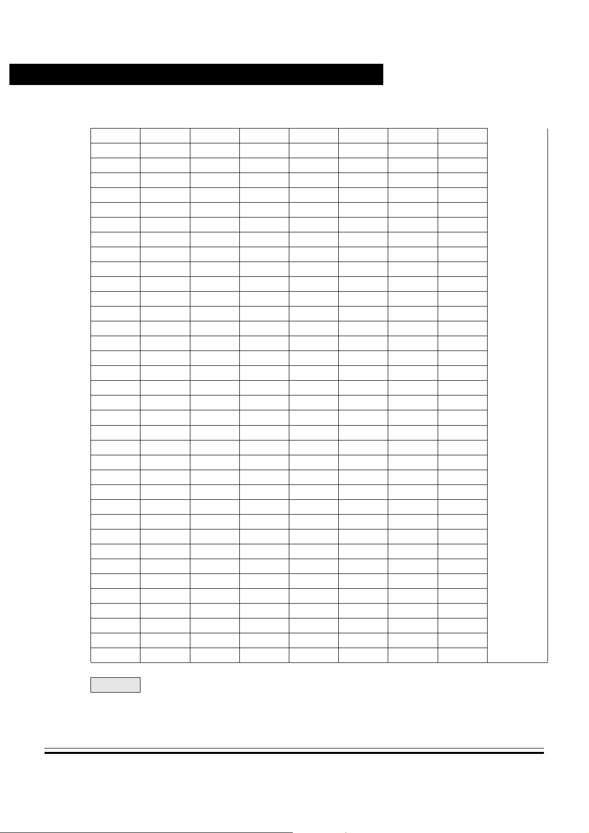
nc...
I
cale Semiconductor,
Frees
Freescale Semiconductor, Inc.
Registers
AddressBit 7654321Bit 0Name
$0096 Bit 15 14 13 12 11 10 9 Bit 8 TC3
$0097Bit 7654321Bit 0TC3
$0098 Bit 15 14 13 12 11 10 9 Bit 8 TC4
$0099Bit 7654321Bit 0TC4
$009A Bit 15 14 13 12 11 10 9 Bit 8 TC5
$009BBit 7654321Bit 0TC5
$009C Bit 15 14 13 12 11 10 9 Bit 8 TC6
$009DBit 7654321Bit 0TC6
$009E Bit 15 14 13 12 11 10 9 Bit 8 TC7
$009FBit 7654321Bit 0TC7
$00A0 0 PAEN PAMOD PEDGE CLK1 CLK0 PAOVI PAI PACTL
$00A1000000PAOVFPAIFPAFLG
$00A2Bit 7654321Bit 0PACN3
$00A3Bit 7654321Bit 0PACN2
$00A4Bit 7654321Bit 0PACN1
$00A5Bit 7654321Bit 0PACN0
$00A6 MCZI MODMC RDMCL ICLAT FLMC MCEN MCPR1 MCPR0 MCCTL
$00A7 MCZF 0 0 0 POLF3 POLF2 POLF1 POLF0 MCFLG
$00A80000PA3ENPA2ENPA1ENPA0ENICPACR
$00A9000000DLY1DLY0DLYCT
$00AA NOVW7 NOVW6 NOVW5 NOVW4 NOVW3 NOVW2 NOVW1 NOVW0 ICOVW
$00AB SH37 SH26 SH15 SH04 TFMOD PACMX BUFEN LATQ ICSYS
$00AC00000000Reserved
$00AD000000TCBYP0TIMTST
$00AE PT7 PT6 PT5 PT4 PT3 PT2 PT1 PT0 PORTT
$00AF DDT7 DDT6 DDT5 DDT4 DDT3 DDT2 DDT1 DDT0 DDRT
$00B0 0 PBEN 0000PBOVI0PBCTL
$00B1000000PBOVF0PBFLG
$00B2Bit 7654321Bit 0PA3H
$00B3Bit 7654321Bit 0PA2H
$00B4Bit 7654321Bit 0PA1H
$00B5Bit 7654321Bit 0PA0H
$00B6 Bit 15 14 13 12 11 10 9 Bit 8 MCCNTH
$00B7Bit 7654321Bit 0MCCNTL
$00B8 Bit 15 14 13 12 11 10 9 Bit 8 TC0H
$00B9Bit 7654321Bit 0TC0H
= Reserved or unimplemented bits.
Table 4-1. MC68HC912D60A Register Map (Sheet 5 of 9)
Technical Data MC68HC912D60A — Rev 3.0
66 Registers MOTOROLA
For More Information On This Product,
Go to: www.freescale.com

nc...
I
cale Semiconductor,
Frees
Freescale Semiconductor, Inc.
AddressBit 7654321Bit 0Name
$00BA Bit 15 14 13 12 11 10 9 Bit 8 TC1H
$00BBBit 7654321Bit 0TC1H
$00BC Bit 15 14 13 12 11 10 9 Bit 8 TC2H
$00BDBit 7654321Bit 0TC2H
$00BE Bit 15 14 13 12 11 10 9 Bit 8 TC3H
$00BFBit 7654321Bit 0TC3H
$00C0 BTST BSPL BRLD SBR12 SBR11 SBR10 SBR9 SBR8 SC0BDH
$00C1 SBR7 SBR6 SBR5 SBR4 SBR3 SBR2 SBR1 SBR0 SC0BDL
$00C2 LOOPS WOMS RSRC M WAKE ILT PE PT SC0CR1
$00C3 TIE TCIE RIE ILIE TE RE RWU SBK SC0CR2
$00C4 TDRE TC RDRF IDLE OR NF FE PF SC0SR1
$00C5 SCSWAI MIE MDL1 MDL0 0 0 0 RAF SC0SR2
$00C6R8T8000000SC0DRH
$00C7 R7/T7 R6/T6 R5/T5 R4/T4 R3/T3 R2/T2 R1/T1 R0/T0 SC0DRL
$00C8 BTST BSPL BRLD SBR12 SBR11 SBR10 SBR9 SBR8 SC1BDH
$00C9 SBR7 SBR6 SBR5 SBR4 SBR3 SBR2 SBR1 SBR0 SC1BDL
$00CA LOOPS WOMS RSRC M WAKE ILT PE PT SC1CR1
$00CB TIE TCIE RIE ILIE TE RE RWU SBK SC1CR2
$00CC TDRE TC RDRF IDLE OR NF FE PF SC1SR1
$00CDSCSWAI000000RAFSC1SR2
$00CER8T8000000SC1DRH
$00CF R7/T7 R6/T6 R5/T5 R4/T4 R3/T3 R2/T2 R1/T1 R0/T0 SC1DRL
$00D0 SPIE SPE SWOM MSTR CPOL CPHA SSOE LSBF SP0CR1
$00D1000000SPSWAI SPC0 SP0CR2
$00D200000SPR2SPR1SPR0SP0BR
$00D3SPIFWCOL0MODF0000SP0SR
$00D4
$00D5Bit 7654321Bit 0SP0DR
$00D6 PS7 PS6 PS5 PS4 PS3 PS2 PS1 PS0 PORTS
$00D7 DDS7 DDS6 DDS5 DDS4 DDS3 DDS2 DDS1 DDS0 DDRS
$00D8
$00D9
$00DA–
$00DF
$00E0–
$00ED
$00EE000000EEDIV9EEDIV8EEDIVH
0 0 0 0 0 0 0 0 Reserved
0 0 0 0 0 0 0 0 Reserved
0 RDPS2 RDPS1 RDPS0 0 PUPS2 PUPS1 PUPS0 PURDS
0 0 0 0 0 0 0 0 Reserved
Unimplemented
(4)
Registers
Register Block
Reserved
= Reserved or unimplemented bits.
Table 4-1. MC68HC912D60A Register Map (Sheet 6 of 9)
MC68HC912D60A — Rev 3.0 Technical Data
MOTOROLA Registers 67
For More Information On This Product,
Go to: www.freescale.com

nc...
I
cale Semiconductor,
Frees
Freescale Semiconductor, Inc.
Registers
AddressBit 7654321Bit 0Name
$00EF EEDIV7 EEDIV6 EEDIV5 EEDIV4 EEDIV3 EEDIV2 EEDIV1 EEDIV0 EEDIVL
$00F0 NOBDML NOSHB
$00F1 SHPROT 1 1 BPROT4 BPROT3 BPROT2 BPROT1 BPROT0 EEPROT
$00F200000000Reserved
$00F3 BULKP 0 AUTO BYTE ROW ERASE EELAT EEPGM EEPROG
$00F40000000LOCKFEE32LCK
$00F50000000BOOTPFEE32MCR
$00F600000000Reserved
$00F7 0 0 0 FEESWAI HVEN 0 ERAS PGM FEE32CTL
$00F80000000LOCKFEE28LCK
$00F90000000BOOTPFEE28MCR
$00FA00000000Reserved
$00FB 0 0 0 FEESWAI HVEN 0 ERAS PGM FEE28CTL
$00FC–
$00FF
$0100 0 0 CSWAI SYNCH TLNKEN SLPAK SLPRQ SFTRES CMCR0
$010100000LOOPBWUPMCLKSRCCMCR1
$0102 SJW1 SJW0 BRP5 BRP4 BRP3 BRP2 BRP1 BRP0 CBTR0
$0103 SAMP TSEG22 TSEG21 TSEG20 TSEG13 TSEG12 TSEG11 TSEG10 CBTR1
$0104 WUPIF RWRNIF TWRNIF RERRIF TERRIF BOFFIF OVRIF RXF CRFLG
$0105 WUPIE RWRNIE TWRNIE RERRIE TERRIE BOFFIE OVRIE RXFIE CRIER
$0106 0 ABTAK2 ABTAK1 ABTAK0 0 TXE2 TXE1 TXE0 CTFLG
$0107 0 ABTRQ2 ABTRQ1 ABTRQ0 0 TXEIE2 TXEIE1 TXEIE0 CTCR
$0108 0 0 IDAM1 IDAM0 0 IDHIT2 IDHIT1 IDHIT0 CIDAC
$0109–
$010D
$010E RXERR7 RXERR6 RXERR5 RXERR4 RXERR3 RXERR2 RXERR1 RXERR0 CRXERR
$010F TXERR7 TXERR6 TXERR5 TXERR4 TXERR3 TXERR2 TXERR1 TXERR0 CTXERR
$0110 AC7 AC6 AC5 AC4 AC3 AC2 AC1 AC0 CIDAR0
$0111 AC7 AC6 AC5 AC4 AC3 AC2 AC1 AC0 CIDAR1
$0112 AC7 AC6 AC5 AC4 AC3 AC2 AC1 AC0 CIDAR2
$0113 AC7 AC6 AC5 AC4 AC3 AC2 AC1 AC0 CIDAR3
$0114AM7AM6AM5AM4AM3AM2AM1AM0CIDMR0
$0115AM7AM6AM5AM4AM3AM2AM1AM0CIDMR1
$0116AM7AM6AM5AM4AM3AM2AM1AM0CIDMR2
$0117AM7AM6AM5AM4AM3AM2AM1AM0CIDMR3
$0118 AC7 AC6 AC5 AC4 AC3 AC2 AC1 AC0 CIDAR4
Reserved
FPOPEN
(5)
Unimplemented
Unimplemented
1 EESWAI PROTLCK DMY EEMCR
(4)
(4)
Reserved
Reserved
= Reserved or unimplemented bits.
Table 4-1. MC68HC912D60A Register Map (Sheet 7 of 9)
Technical Data MC68HC912D60A — Rev 3.0
68 Registers MOTOROLA
For More Information On This Product,
Go to: www.freescale.com

nc...
I
cale Semiconductor,
Frees
Freescale Semiconductor, Inc.
AddressBit 7654321Bit 0Name
$0119 AC7 AC6 AC5 AC4 AC3 AC2 AC1 AC0 CIDAR5
$011A AC7 AC6 AC5 AC4 AC3 AC2 AC1 AC0 CIDAR6
$011B AC7 AC6 AC5 AC4 AC3 AC2 AC1 AC0 CIDAR7
$011C AM7 AM6 AM5 AM4 AM3 AM2 AM1 AM0 CIDMR4
$011D AM7 AM6 AM5 AM4 AM3 AM2 AM1 AM0 CIDMR5
$011EAM7AM6AM5AM4AM3AM2AM1AM0CIDMR6
$011F AM7 AM6 AM5 AM4 AM3 AM2 AM1 AM0 CIDMR7
$0120–
$013C
$013D000000PUPCANRDPCANPCTLCAN
$013E PCAN7 PCAN6 PCAN5 PCAN4 PCAN3 PCAN2 TxCAN RxCAN PORTCAN
$013F DDCAN7 DDCAN6 DDCAN5 DDCAN4 DDCAN3 DDCAN2 0 0 DDRCAN
$0140–
$014F
$0150–
$015F
$0160–
$016F
$0170–
$017F
$0180–
$01DF
$01E0
$01E1
$01E2 ADPU AFFC ASWAI DJM
$01E30000S1CFIFOFRZ1FRZ0ATD1CTL3
$01E4 RES10 SMP1 SMP0 PRS4 PRS3 PRS2 PRS1 PRS0 ATD1CTL4
$01E5 0 S8C SCAN MULT SC CC CB CA ATD1CTL5
$01E6SCF0000CC2CC1CC0ATD1STAT0
$01E7 CCF7 CCF6 CCF5 CCF4 CCF3 CCF2 CCF1 CCF0 ATD1STAT1
$01E8 SAR9 SAR8 SAR7 SAR6 SAR5 SAR4 SAR3 SAR2 ATD1TESTH
$01E9 SAR1 SAR0 RST TSTOUT TST3 TST2 TST1 TST0 ATD1TESTL
$01EA–$
01EE
$01EF PAD17 PAD16 PAD15 PAD14 PAD13 PAD12 PAD11 PAD10 PORTAD1
0 0 0 0 0 0 0 0 Reserved
Register Block
Unimplemented
RECEIVE BUFFER RxFG
TRANSMIT BUFFER 0 Tx0
TRANSMIT BUFFER 1 Tx1
TRANSMIT BUFFER 2 Tx2
Unimplemented
Reserved ATD1CTL0
Reserved ATD1CTL1
(4)
(4)
R R ASCIE ASCIF ATD1CTL2
Reserved
Reserved
Registers
= Reserved or unimplemented bits.
Table 4-1. MC68HC912D60A Register Map (Sheet 8 of 9)
MC68HC912D60A — Rev 3.0 Technical Data
MOTOROLA Registers 69
For More Information On This Product,
Go to: www.freescale.com

nc...
I
Freescale Semiconductor, Inc.
Registers
AddressBit 7654321Bit 0Name
$01F0 Bit 15 14 13 12 11 10 9 Bit 8 ADR10H
$01F1Bit 7Bit 6000000ADR10L
$01F2 Bit 15 14 13 12 11 10 9 Bit 8 ADR11H
$01F3Bit 7Bit 6000000ADR11L
$01F4 Bit 15 14 13 12 11 10 9 Bit 8 ADR12H
$01F5Bit 7Bit 6000000ADR12L
$01F6 Bit 15 14 13 12 11 10 9 Bit 8 ADR13H
$01F7Bit 7Bit 6000000ADR13L
$01F8 Bit 15 14 13 12 11 10 9 Bit 8 ADR14H
$01F9Bit 7Bit 6000000ADR14L
$01FA Bit 15 14 13 12 11 10 9 Bit 8 ADR15H
$01FBBit 7Bit 6000000ADR15L
$01FC Bit 15 14 13 12 11 10 9 Bit 8 ADR16H
$01FDBit 7Bit 6000000ADR16L
$01FE Bit 15 14 13 12 11 10 9 Bit 8 ADR17H
$01FFBit 7Bit 6000000ADR17L
cale Semiconductor,
Frees
= Reserved or unimplemented bits.
1. Port A, port B and data direction registers DDRA, DDRB are not in map in expanded and peripheral modes.
2. Port E and DDRE not in map in peripheral mode; also not in map in expanded modes with EME set.
3. Registers also not in map in peripheral mode.
4. Data read at these locations is undefined.
5. The FPOPEN bit is available only on the 1L02H and later mask sets. For previous masks, this bit is reserved.
Table 4-1. MC68HC912D60A Register Map (Sheet 9 of 9)
Technical Data MC68HC912D60A — Rev 3.0
70 Registers MOTOROLA
For More Information On This Product,
Go to: www.freescale.com

Freescale Semiconductor, Inc.
Technical Data — MC68HC912D60A
Section 5. Operating Modes and Resource Mapping
5.1 Contents
5.2 Introduction . . . . . . . . . . . . . . . . . . . . . . . . . . . . . . . . . . . . . . . .71
5.3 Operating Modes . . . . . . . . . . . . . . . . . . . . . . . . . . . . . . . . . . .71
nc...
I
5.2 Introduction
cale Semiconductor,
5.3 Operating Modes
Frees
5.4 Background Debug Mode . . . . . . . . . . . . . . . . . . . . . . . . . . . . .74
5.5 Internal Resource Mapping. . . . . . . . . . . . . . . . . . . . . . . . . . . .77
5.6 Memory Maps . . . . . . . . . . . . . . . . . . . . . . . . . . . . . . . . . . . . . .83
Eight possible operating modes determine the operating configuration of
the MC68HC912D60A. Each mode has an associated default memory
map and external bus configuration. After reset, most system resources
can be mapped to other addresses by writing to the appropriate control
registers.
The operating mode out of reset is determined by the states of the
BKGD, MODB, and MODA pins during reset.
The SMODN, MODB, and MODA bits in the MODE register show current
operating mode and provide limited mode switching during operation.
MC68HC912D60A — Rev 3.0 Technical Data
MOTOROLA Operating Modes and Resource Mapping 71
For More Information On This Product,
Go to: www.freescale.com

Freescale Semiconductor, Inc.
Operating Modes and Resource Mapping
The states of the BKGD, MODB, and MODA pins are latched into these
bits on the rising edge of the reset signal.
Table 5-1. Mode Selection
BKGD MODB MODA Mode Port A Port B
1 0 0 Normal Single Chip G.P. I/O G.P. I/O
1 0 1 Normal Expanded Narrow ADDR/DATA ADDR
nc...
I
cale Semiconductor,
Frees
110
1 1 1 Normal Expanded Wide ADDR/DATA ADDR/DATA
0 0 0 Special Single Chip G.P. I/O G.P. I/O
0 0 1 Special Expanded Narrow ADDR/DATA ADDR
0 1 0 Special Peripheral ADDR/DATA ADDR/DATA
0 1 1 Special Expanded Wide ADDR/DATA ADDR/DATA
There are two basic types of operating modes:
Normal modes — some registers and bits are protected
against accidental changes.
Special modes — allow greater access to protected control
registers and bits for special purposes such as testing and
emulation.
For operation above 105°C, the MC68HC912D60A (M temperature
range product only) is limited to single chip modes of operation.
Reserved (Forced to
Peripheral)
——
A system development and debug feature, background debug mode
(BDM), is available in all modes. In special single-chip mode, BDM is
active immediately after reset.
5.3.1 Normal Operating Modes
These modes provide three operating configurations. Background
debugging is available in all three modes, but must first be enabled for
some operations by means of a BDM background command, then
activated.
Technical Data MC68HC912D60A — Rev 3.0
72 Operating Modes and Resource Mapping MOTOROLA
For More Information On This Product,
Go to: www.freescale.com

Freescale Semiconductor, Inc.
nc...
I
Operating Modes and Resource Mapping
Operating Modes
Normal Single-Chip Mode — There are no external address
and data buses in this mode. The MCU operates as a standalone device and all program and data resources are on-chip.
External port pins normally associated with address and data
buses can be used for general-purpose I/O.
Normal Expanded Wide Mode — This is a normal mode of
operation in which the expanded bus is present with a 16-bit
data bus. Ports A and B are used for the 16-bit multiplexed
address/data bus.
Normal Expanded Narrow Mode — This is a normal mode of
operation in which the expanded bus is present with an 8-bit
data bus. Ports A and B are used for the16-bit address bus.
Port A is used as the data bus, multiplexed with addresses. In
this mode, 16-bit data is presented one byte at a time, the high
byte followed by the low byte. The address is automatically
incremented on the second cycle.
5.3.2 Special Operating Modes
cale Semiconductor,
Frees
There are three special operating modes that correspond to normal
operating modes. These operating modes are commonly used in factory
testing and system development. In addition, there is a special
peripheral mode, in which an external master, such as an I.C. tester, can
control the on-chip peripherals.
Special Single-Chip Mode — This mode can be used to force
the MCU to active BDM mode to allow system debug through
the BKGD pin. There are no external address and data buses
in this mode. The MCU operates as a stand-alone device and
all program and data space are on-chip. External port pins can
be used for general-purpose I/O.
Special Expanded Wide Mode — This mode can be used for
emulation of normal expanded wide mode and emulation of
normal single-chip mode. Ports A and B are used for the 16-bit
multiplexed address/data bus.
MC68HC912D60A — Rev 3.0 Technical Data
MOTOROLA Operating Modes and Resource Mapping 73
For More Information On This Product,
Go to: www.freescale.com

Freescale Semiconductor, Inc.
Operating Modes and Resource Mapping
Special Expanded Narrow Mode — This mode can be used
for emulation of normal expanded narrow mode. Ports A and B
are used for the16-bit address bus. Port A is used as the data
bus, multiplexed with addresses. In this mode, 16-bit data is
presented one byte at a time, the high byte followed by the low
byte. The address is automatically incremented on the second
cycle.
Special Peripheral Mode — The CPU is not active in this
mode. An external master can control on-chip peripherals for
testing purposes. It is not possible to change to or from this
mode without going through reset. Background debugging
nc...
I
should not be used while the MCU is in special peripheral
mode as internal bus conflicts between BDM and the external
master can cause improper operation of both modes.
5.4 Background Debug Mode
cale Semiconductor,
Background debug mode (BDM) is an auxiliary operating mode that is
used for system development. BDM is implemented in on-chip hardware
and provides a full set of debug operations. Some BDM commands can
be executed while the CPU is operating normally. Other BDM
commands are firmware based, and require the BDM firmware to be
enabled and active for execution.
In special single-chip mode, BDM is enabled and active immediately out
of reset. BDM is available in all other operating modes, but must be
enabled before it can be activated. BDM should not be used in special
peripheral mode because of potential bus conflicts.
Frees
Once enabled, background mode can be made active by a serial
command sent via the BKGD pin or execution of a CPU12 BGND
instruction. While background mode is active, the CPU can interpret
special debugging commands, and read and write CPU registers,
peripheral registers, and locations in memory.
While BDM is active, the CPU executes code located in a small on-chip
ROM mapped to addresses $FF20 to $FFFF, and BDM control registers
are accessible at addresses $FF00 to $FF06. The BDM ROM replaces
Technical Data MC68HC912D60A — Rev 3.0
74 Operating Modes and Resource Mapping MOTOROLA
For More Information On This Product,
Go to: www.freescale.com

Freescale Semiconductor, Inc.
Operating Modes and Resource Mapping
Background Debug Mode
the regular system vectors while BDM is active. While BDM is active, the
user memory from $FF00 to $FFFF is not in the map except through
serial BDM commands.
Bit 7654321Bit 0
SMODN MODB MODA ESTR IVIS EBSWAI 0 EME
RESET:00011001Special Single Chip
RESET:00111001Special Exp Nar
RESET:01011001 Peripheral
nc...
I
RESET:01111001Special Exp Wide
RESET:10010000Normal Single Chip
RESET:10110000Normal Exp Nar
RESET:11110000Normal Exp Wide
MODE — Mode Register $000B
MODE controls the MCU operating mode and various configuration
options. This register is not in the map in peripheral mode
SMODN, MODB, MODA — Mode Select Special, B and A
These bits show the current operating mode and reflect the status of
the BKGD, MODB and MODA input pins at the rising edge of reset.
cale Semiconductor,
SMODN is Read anytime. May only be written in special modes
(SMODN = 0). The first write is ignored;
MODB, MODA may be written once in Normal modes (SMODN = 1).
Frees
Write anytime in special modes (first write is ignored) – special
peripheral and reserved modes cannot be selected.
MC68HC912D60A — Rev 3.0 Technical Data
MOTOROLA Operating Modes and Resource Mapping 75
For More Information On This Product,
Go to: www.freescale.com

Freescale Semiconductor, Inc.
Operating Modes and Resource Mapping
ESTR — E Clock Stretch Enable
Determines if the E Clock behaves as a simple free-running clock or
as a bus control signal that is active only for external bus cycles.
ESTR is always 1 in expanded modes since it is required for address
and data bus de-multiplexing and must follow stretched cycles.
0 = E never stretches (always free running).
1 = E stretches high during external access cycles and low during
non-visible internal accesses (IVIS=0).
Normal modes: write once; Special modes: write anytime. Read
anytime.
nc...
I
cale Semiconductor,
Frees
IVIS — Internal Visibility
This bit determines whether internal ADDR, DATA, R/W and LSTRB
signals can be seen on the external bus during accesses to internal
locations. In Special Narrow Mode if this bit is set and an internal
access occurs the data will appear wide on Ports A and B. This serves
the same function as the EMD bit of the non-multiplexed versions of
the HC12 and allows for emulation. Visibility is not available when the
part is operating in a single-chip mode.
0 = No visibility of internal bus operations on external bus.
1 = Internal bus operations are visible on external bus.
Normal modes: write once; Special modes: write anytime EXCEPT
the first time. Read anytime.
EBSWAI — External Bus Module Stop in Wait Control
This bit controls access to the external bus interface when in wait
mode. The module will delay before shutting down in wait mode to
allow for final bus activity to complete.
0 = External bus and registers continue functioning during wait mode.
1 = External bus is shut down during wait mode.
Normal modes: write anytime; Special modes: write never. Read
anytime.
Technical Data MC68HC912D60A — Rev 3.0
76 Operating Modes and Resource Mapping MOTOROLA
For More Information On This Product,
Go to: www.freescale.com

EME — Emulate Port E
nc...
5.5 Internal Resource Mapping
I
Freescale Semiconductor, Inc.
In single-chip mode PORTE and DDRE are always in the map
regardless of the state of this bit.
0 = PORTE and DDRE are in the memory map.
1 = If in an expanded mode, PORTE and DDRE are removed from the
internal memory map. Removing the registers from the map allows
the user to emulate the function of these registers externally.
Normal modes: write once; special modes: write anytime EXCEPT
the first time. Read anytime.
Operating Modes and Resource Mapping
Internal Resource Mapping
cale Semiconductor,
Frees
The internal register block, RAM, and EEPROM have default locations
within the 64K byte standard address space but may be reassigned to
other locations during program execution by setting bits in mapping
registers INITRG, INITRM, and INITEE. During normal operating modes
these registers can be written once. It is advisable to explicitly establish
these resource locations during the initialization phase of program
execution, even if default values are chosen, in order to protect the
registers from inadvertent modification later.
Writes to the mapping registers go into effect between the cycle that
follows the write and the cycle after that. To assure that there are no
unintended operations, a write to one of these registers should be
followed with a NOP instruction.
If conflicts occur when mapping resources, the register block will take
precedence over the other resources; RAM or EEPROM addresses
occupied by the register block will not be available for storage. When
active, BDM ROM takes precedence over other resources, although a
conflict between BDM ROM and register space is not possible. The
following table shows resource mapping precedence.
In expanded modes, all address space not used by internal resources is
by default external memory.
The MC68HC912D60A contains 60K bytes of Flash EEPROM
nonvolatile memory which can be used to store program code or static
MC68HC912D60A — Rev 3.0 Technical Data
MOTOROLA Operating Modes and Resource Mapping 77
For More Information On This Product,
Go to: www.freescale.com

Freescale Semiconductor, Inc.
Operating Modes and Resource Mapping
data. It is made of the 28K byte FEE28 array mapped from $1000 to
$7FFF at reset and of the 32 K byte FEE32 array mapped from $8000 to
$FFFF at reset. MAPROM bit in the MISC register allows the swapping
of the two flash arrays.
Precedence Resource
1 BDM ROM (if active)
2 Register Space
nc...
I
3RAM
4 EEPROM
Table 5-2. Mapping Precedence
5 On-Chip Flash EEPROM (MC68HC912D60A)
6 External Memory
5.5.1 Register Block Mapping
After reset the 512 byte register block resides at location $0000 but can
be reassigned to any 2K byte boundary within the standard 64K byte
address space. Mapping of internal registers is controlled by five bits in
the INITRG register. The register block occupies the first 512 bytes of the
2K byte block.
cale Semiconductor,
Bit 7654321Bit 0
REG15 REG14 REG13 REG12 REG11 0 0 MMSWAI
Frees
RESET: 0 0 0 0 0 0 0 0
INITRG — Initialization of Internal Register Position Register $0011
REG[15:11] — Internal register map position
These bits specify the upper five bits of the 16-bit registers address.
Normal modes: write once; special modes: write anytime. Read
anytime.
Technical Data MC68HC912D60A — Rev 3.0
78 Operating Modes and Resource Mapping MOTOROLA
For More Information On This Product,
Go to: www.freescale.com

nc...
5.5.2 RAM Mapping
I
Freescale Semiconductor, Inc.
MMSWAI — Memory Mapping Interface Stop in Wait Control
This bit controls access to the memory mapping interface when in
Wait mode.
Normal modes: write anytime; special modes: write never. Read
anytime.
0 = Memory mapping interface continues to function during Wait
mode.
1 = Memory mapping interface access is shut down during Wait
mode.
Operating Modes and Resource Mapping
Internal Resource Mapping
The MC68HC912D60A has 2K byte of fully static RAM that is used for
storing instructions, variables, and temporary data during program
execution. After reset, RAM addressing begins at location $0000 but can
be assigned to any 2K byte boundary within the standard 64K byte
address space. Mapping of internal RAM is controlled by five bits in the
INITRM register.
After reset, the first 512 bytes of RAM have their access inhibited by the
presence of the register address space. After initial MCU configuration,
it is recommended to map the register space at location $0800.
Bit 7654321Bit 0
cale Semiconductor,
RESET:00000000
INITRM — Initialization of Internal RAM Position Register $0010
RAM15 RAM14 RAM13 RAM12 RAM11 0 0 0
Frees
RAM[15:11] — Internal RAM map position
These bits specify the upper five bits of the 16-bit RAM address.
Normal modes: write once; special modes: write anytime. Read
anytime.
MC68HC912D60A — Rev 3.0 Technical Data
MOTOROLA Operating Modes and Resource Mapping 79
For More Information On This Product,
Go to: www.freescale.com

Freescale Semiconductor, Inc.
Operating Modes and Resource Mapping
5.5.3 EEPROM Mapping
The MC68HC912D60A has 1K bytes of EEPROM which is activated by
the EEON bit in the INITEE register. Mapping of internal EEPROM is
controlled by four bits in the INITEE register. After reset EEPROM
address space begins at location $0C00 but can be mapped to any 4K
byte boundary within the standard 64K byte address space.
Bit 7654321Bit 0
EE15 EE14 EE13 EE12 0 0 0 EEON
RESET:00000001
INITEE— Initialization of Internal EEPROM Position Register $0012
nc...
I
cale Semiconductor,
Frees
EE[15:12] — Internal EEPROM map position
These bits specify the upper four bits of the 16-bit EEPROM address.
Normal modes: write once; special modes: write anytime. Read
anytime.
EEON — internal EEPROM On (Enabled)
This bit is forced to one in single-chip modes.
Read or write anytime.
0 = Removes the EEPROM from the map.
1 = Places the on-chip EEPROM in the memory map at the address
selected by EE[15:12].
Technical Data MC68HC912D60A — Rev 3.0
80 Operating Modes and Resource Mapping MOTOROLA
For More Information On This Product,
Go to: www.freescale.com

Freescale Semiconductor, Inc.
5.5.4 Miscellaneous System Control Register
Additional mapping and external resource controls are available. To use
external resources the part must be operated in one of the expanded
modes.
Bit 7654321Bit 0
MAPROM NDRF RFSTR1 RFSTR0 EXSTR1 EXSTR0 ROMON28 ROMON32
RESET: 0 0 0 0 1 1 0 0 Exp Modes
RESET: 0 0 0 0 1 1 1 1 SC Modes
MISC — Miscellaneous Mapping Control Register $0013
nc...
I
Normal modes: write once; Special modes: write anytime. Read
anytime.
Operating Modes and Resource Mapping
Internal Resource Mapping
cale Semiconductor,
Frees
MAPROM — Map Location of ROM
This bit is used to swap the location of the on-chip Flash EEPROM.
0 = 28K byte array is mapped from $1000 to $7FFF, 32K byte array
is mapped from $8000 to $FFFF.
1 = 28K byte is mapped from $9000 to $FFFF, 32K byte array is
mapped from $0000 to $7FFF.
NDRF — Narrow Data Bus for Register-Following Map Space
This bit enables a narrow bus feature for the 512 byte RegisterFollowing Map. This is useful for accessing 8-bit peripherals and
allows 8-bit and 16-bit external memory devices to be mixed in a
system. In Expanded Narrow (eight bit) modes, Single Chip Modes,
and Peripheral mode, this bit has no effect.
0 = Makes Register-Following MAP space act as a full 16 bit data bus.
1 = Makes the Register-Following MAP space act the same as an 8
bit only external data bus (data only goes through port A externally).
The Register-Following space is mapped from $0200 to $03FF after
reset, which is next to the register map. If the registers are moved this
space follows.
MC68HC912D60A — Rev 3.0 Technical Data
MOTOROLA Operating Modes and Resource Mapping 81
For More Information On This Product,
Go to: www.freescale.com

Freescale Semiconductor, Inc.
Operating Modes and Resource Mapping
RFSTR1, RFSTR0 — Register Following Stretch
This two bit field determines the amount of clock stretch on accesses
to the 512 byte Register Following Map. It is valid regardless of the
state of the NDRF bit. In Single Chip and Peripheral Modes this bit
has no meaning or effect.
Table 5-3. RFSTR Stretch Bit Definition
RFSTR1 RFSTR0
00 0
01 1
nc...
I
10 2
11 3
Number of E Clocks
Stretched
EXSTR1, EXSTR0 — External Access Stretch
This two bit field determines the amount of clock stretch on accesses
to the External Address Space. In Single Chip and Peripheral Modes
this bit has no meaning or effect.
Table 5-4. EXSTR Stretch Bit Definition
EXSTR1 EXSTR0
00 0
cale Semiconductor,
01 1
10 2
11 3
Number of E Clocks
Stretched
Frees
ROMON28, ROMON32 — Enable bits for ROM
These bits are used to enable the Flash EEPROM arrays FEE28 and
FEE32 respectively.
0 = Corresponding Flash EEPROM array disabled from the memory
map.
1 = Corresponding Flash EEPROM array enabled in the memory
map.
Technical Data MC68HC912D60A — Rev 3.0
82 Operating Modes and Resource Mapping MOTOROLA
For More Information On This Product,
Go to: www.freescale.com
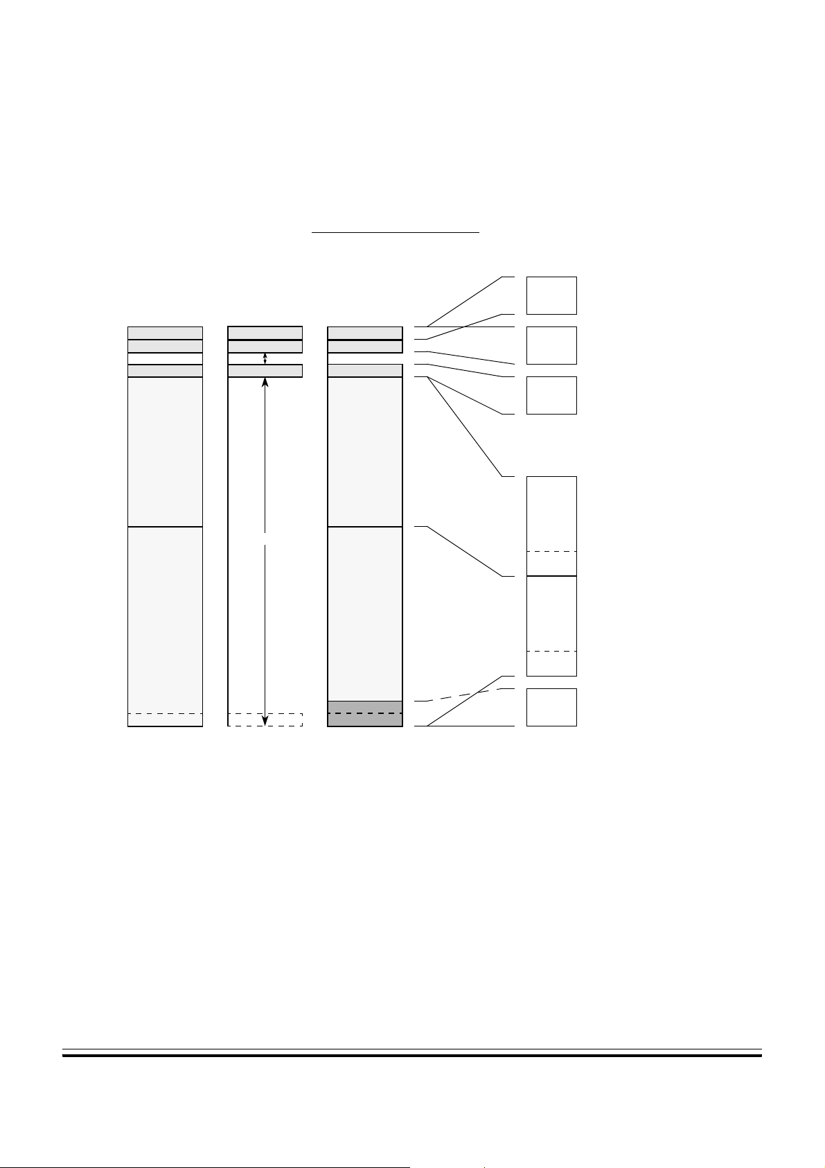
5.6 Memory Maps
Freescale Semiconductor, Inc.
Operating Modes and Resource Mapping
Memory Maps
The following diagrams illustrate the memory map for each mode of
operation immediately after reset.
$0000
$01FF
$0000
$0200
$0800
$0C00
$1000
nc...
I
$8000
EXT
cale Semiconductor,
$FF00
$FFFF
SINGLE CHIP
VECTORSVECTORS
EXPANDEDNORMAL
VECTORS
SPECIAL
SINGLE CHIP
$0000
$07FF
$0C00
$0FFF
$1000
$7FFF
$8000
$FFFF
$FF00
$FFFF
REGISTERS
(MAPPABLE TO ANY 2K SPACE)
2K bytes RAM
(MAPPABLE TO ANY 2K SPACE)
1K bytes EEPROM
(MAPPABLE TO ANY 4K SPACE)
28K Flash EEPROM (FEE28)
$6000 - $7FFF Protected BOOT
32K Flash EEPROM
$E000 –$FFFF Protected BOOT
BDM
(if active)
(FEE32)
Frees
MC68HC912D60A — Rev 3.0 Technical Data
MOTOROLA Operating Modes and Resource Mapping 83
Figure 5-1
For More Information On This Product,
. MC68HC912D60A Memory Map
Go to: www.freescale.com

Freescale Semiconductor, Inc.
Operating Modes and Resource Mapping
nc...
I
cale Semiconductor,
Frees
Technical Data MC68HC912D60A — Rev 3.0
84 Operating Modes and Resource Mapping MOTOROLA
For More Information On This Product,
Go to: www.freescale.com

Freescale Semiconductor, Inc.
Technical Data — MC68HC912D60A
Section 6. Bus Control and Input/Output
6.1 Contents
6.2 Introduction . . . . . . . . . . . . . . . . . . . . . . . . . . . . . . . . . . . . . . . .85
6.3 Detecting Access Type from External Signals . . . . . . . . . . . . .85
nc...
I
6.4 Registers. . . . . . . . . . . . . . . . . . . . . . . . . . . . . . . . . . . . . . . . . .86
6.2 Introduction
Internally the MC68HC912D60A has full 16-bit data paths, but
depending upon the operating mode and control registers, the external
multiplexed bus may be 8 or 16 bits. There are cases where 8-bit and
16-bit accesses can appear on adjacent cycles using the LSTRB signal
to indicate 8- or 16-bit data.
It is possible to have a mix of 8 and 16 bit peripherals attached to the
external multiplexed bus, using the NDRF bit in the MISC register while
in expanded wide modes.
cale Semiconductor,
6.3 Detecting Access Type from External Signals
Frees
The external signals LSTRB, R/W, and A0 can be used to determine the
type of bus access that is taking place. Accesses to the internal RAM
module are the only type of access that produce LSTRB
because the internal RAM is specifically designed to allow misaligned
16-bit accesses in a single cycle. In these cases the data for the address
=A0=1,
MC68HC912D60A — Rev 3.0 Technical Data
MOTOROLA Bus Control and Input/Output 85
For More Information On This Product,
Go to: www.freescale.com

Bus Control and Input/Output
that was accessed is on the low half of the data bus and the data for
address + 1 is on the high half of the data bus.
nc...
I
Freescale Semiconductor, Inc.
Figure 6-1. Access Type vs. Bus Control Pins
LSTRB A0 R/W Type of Access
1 0 1 8-bit read of an even address
0 1 1 8-bit read of an odd address
1 0 0 8-bit write of an even address
0 1 0 8-bit write of an odd address
0 0 1 16-bit read of an even address
111
0 0 0 16-bit write to an even address
110
16-bit read of an odd address
(low/high data swapped)
16-bit write to an even address
(low/high data swapped)
6.4 Registers
cale Semiconductor,
Frees
Not all registers are visible in the MC68HC912D60A memory map under
certain conditions. In special peripheral mode the first 16 registers
associated with bus expansion are removed from the memory map.
In expanded modes, some or all of port A, port B, and port E are used
for expansion buses and control signals. In order to allow emulation of
the single-chip functions of these ports, some of these registers must be
rebuilt in an external port replacement unit. In any expanded mode, port
A, and port B, are used for address and data lines so registers for these
ports, as well as the data direction registers for these ports, are removed
from the on-chip memory map and become external accesses.
In any expanded mode, port E pins may be needed for bus control (e.g.,
ECLK, R/W). To regain the single-chip functions of port E, the emulate
port E (EME) control bit in the MODE register may be set. In this special
case of expanded mode and EME set, PORTE and DDRE registers are
removed from the on-chip memory map and become external accesses
so port E may be rebuilt externally.
Technical Data MC68HC912D60A — Rev 3.0
86 Bus Control and Input/Output MOTOROLA
For More Information On This Product,
Go to: www.freescale.com

Freescale Semiconductor, Inc.
Bit 7654321Bit 0
Single Chip PA7 PA6 PA5 PA4 PA3 PA2 PA1 PA0
RESET: — — — — — — — —
Bus Control and Input/Output
Registers
Expanded
& Periph:
Expanded
narrow
PORTA — Port A Register $0000
nc...
I
ADDR15/
DATA15
ADDR15/
DATA15/
DATA7
ADDR14/
DATA14
ADDR14/
DATA14/
DATA6
ADDR13/
DATA13
ADDR13/
DATA13/
DATA5
ADDR12/
DATA12
ADDR12/
DATA12/
DATA4
ADDR11/
DATA11
ADDR11/
DATA11/
DATA3
ADDR10/
DATA10
ADDR10/
DATA10/
DATA2
ADDR9/
DATA9
ADDR9/
DATA9/
DATA1
ADDR8/
DATA8
ADDR8/
DATA8/
DATA0
Bits PA[7:0] are associated respectively with addresses ADDR[15:8],
DATA[15:8] and DATA[7:0], in narrow mode. When this port is not used
for external addresses such as in single-chip mode, these pins can be
used as general-purpose I/O. DDRA determines the primary direction of
each pin. This register is not in the on-chip map in expanded and
peripheral modes. Read and write anytime.
Bit 7654321Bit 0
DDA7 DDA6 DDA5 DDA4 DDA3 DDA2 DDA1 DDA0
RESET: 00000000
DDRA — Port A Data Direction Register $0002
cale Semiconductor,
This register determines the primary direction for each port A pin when
functioning as a general-purpose I/O port. DDRA is not in the on-chip
Frees
map in expanded and peripheral modes. Read and write anytime.
0 = Associated pin is a high-impedance input
1 = Associated pin is an output
MC68HC912D60A — Rev 3.0 Technical Data
MOTOROLA Bus Control and Input/Output 87
For More Information On This Product,
Go to: www.freescale.com

Freescale Semiconductor, Inc.
Bus Control and Input/Output
Bit 7654321Bit 0
Single Chip PB7 PB6 PB5 PB4 PB3 PB2 PB1 PB0
RESET: — — — — — — — —
Expanded
& Periph:
Expanded
narrow
PORTB — Port B Register $0001
nc...
I
ADDR7/
DATA7
ADDR7 ADDR6 ADDR5 ADDR4 ADDR3 ADDR2 ADDR1 ADDR0
ADDR6/
DATA6
ADDR5/
DATA5
ADDR4/
DATA4
ADDR3/
DATA3
ADDR2/
DATA2
ADDR1/
DATA1
ADDR0/
DATA0
Bits PB[7:0] are associated with addresses ADDR[7:0] and DATA[7:0]
(except in narrow mode) respectively. When this port is not used for
external addresses such as in single-chip mode, these pins can be used
as general-purpose I/O. DDRB determines the primary direction of each
pin. This register is not in the on-chip map in expanded and peripheral
modes. Read and write anytime.
Bit 7654321Bit 0
DDB7 DDB6 DDB5 DDB4 DDB3 DDB2 DDB1 DDB0
RESET: 00000000
DDRB — Port B Data Direction Register $0003
cale Semiconductor,
This register determines the primary direction for each port B pin when
functioning as a general-purpose I/O port. DDRB is not in the on-chip
Frees
map in expanded and peripheral modes. Read and write anytime.
0 = Associated pin is a high-impedance input
1 = Associated pin is an output
Technical Data MC68HC912D60A — Rev 3.0
88 Bus Control and Input/Output MOTOROLA
For More Information On This Product,
Go to: www.freescale.com

Freescale Semiconductor, Inc.
BIT 7654321BIT 0
PE7 PE6 PE5 PE4 PE3 PE2 PE1 PE0
RESET: — — — —————
Bus Control and Input/Output
Registers
or
or
MODB or
IPIPE1 or
CGMTST
MODA or
IPIPE0
ECLK
Alt. Pin
Function
PORTE — Port E Register $0008
DBE
ECLK
CAL
LSTRB
or
BDTAGL or
TAGLO
R/W IRQ XIRQ
This register is associated with external bus control signals and interrupt
nc...
I
inputs, including data bus enable (DBE
MODA/IPIPE0), ECLK, size (LSTRB), read/write (R/W), IRQ, and XIRQ.
), mode select (MODB/IPIPE1,
When the associated pin is not used for one of these specific functions,
the pin can be used as general-purpose I/O. The port E assignment
register (PEAR) selects the function of each pin. DDRE determines the
primary direction of each port E pin when configured to be generalpurpose I/O.
Some of these pins have software selectable pull-ups (DBE, LSTRB,
R/W, IRQ, and XIRQ). A single control bit enables the pull-ups for all
these pins which are configured as inputs.
This register is not in the map in peripheral mode or expanded modes
when the EME bit is set.
cale Semiconductor,
Read and write anytime.
Frees
Bit 7654321Bit 0
DDE7 DDE6 DDE5 DDE4 DDE3 DDE2 0 0
RESET:00000000
DDRE — Port E Data Direction Register $0009
This register determines the primary direction for each port E pin
configured as general-purpose I/O.
MC68HC912D60A — Rev 3.0 Technical Data
MOTOROLA Bus Control and Input/Output 89
For More Information On This Product,
Go to: www.freescale.com

Bus Control and Input/Output
PE[1:0] are associated with XIRQ and IRQ and cannot be configured as
outputs. These pins can be read regardless of whether the alternate
interrupt functions are enabled.
This register is not in the map in peripheral mode and expanded modes
while the EME control bit is set.
Read and write anytime.
nc...
I
BIT 7654321BIT 0
Freescale Semiconductor, Inc.
0 = Associated pin is a high-impedance input
1 = Associated pin is an output
NDBE CGMTE PIPOE NECLK LSTRE RDWE CALE DBENE
RESET: 00000000
RESET: 00101100
RESET: 11010000Peripheral
RESET: 10010000
RESET: 00101100
PEAR — Port E Assignment Register $000A
cale Semiconductor,
The PEAR register is used to choose between the general-purpose I/O
functions and the alternate bus control functions of port E. When an
alternate control function is selected, the associated DDRE bits are
Frees
overridden.
The reset condition of this register depends on the mode of operation
because bus-control signals are needed immediately after reset in some
modes.
Normal
Expanded
Special
Expanded
Normal
single chip
Special
single chip
In normal single-chip mode, no external bus control signals are needed
so all of port E is configured for general-purpose I/O.
Technical Data MC68HC912D60A — Rev 3.0
90 Bus Control and Input/Output MOTOROLA
For More Information On This Product,
Go to: www.freescale.com

Freescale Semiconductor, Inc.
In normal expanded modes, the reset vector is located in external
memory. The DBE and ECLK are required for de-multiplexing address
and data, but LSTRB and R/W are only needed by the system when
there are external writable resources. Therefore in normal expanded
modes, only the DBE and ECLK are configured for their alternate bus
control functions and the other bits of port E are configured for generalpurpose I/O. If the normal expanded system needs any other bus-control
signals, PEAR would need to be written before any access that needed
the additional signals.
In special expanded modes, DBE, IPIPE1, IPIPE0, E, LSTRB, and R/W
are configured as bus-control signals.
nc...
I
In peripheral mode, the PEAR register is not accessible for reads or
writes. However, the CGMTE control bit is reset to one to configure PE6
as a test output from the PLL module.
Bus Control and Input/Output
Registers
cale Semiconductor,
Frees
NDBE — No Data Bus Enable
Normal: write once; Special: write anytime EXCEPT the first. Read
anytime.
0 = PE7 is used for DBE, external control of data enable on
memories, or inverted ECLK.
1 = PE7 is the CAL function if CALE bit is set in PEAR register or
general-purpose I/O.
NDBE controls the use of the DBE
effect in Single Chip or Peripheral Modes. The associated pin will
default to the CAL function if the CALE bit is set in PEAR register or
otherwise to an I/O.
CGMTE — Clock Generator Module Testing Enable
Normal: write never; Special: write anytime EXCEPT the first. Read
anytime.
0 = PE6 is general-purpose I/O or pipe output.
1 = PE6 is a test signal output from the CGM module (no effect in
single chip or normal expanded modes). PIPOE = 1 overrides
this function and forces PE6 to be a pipe status output signal.
pin of Port E. The NDBE bit has no
MC68HC912D60A — Rev 3.0 Technical Data
MOTOROLA Bus Control and Input/Output 91
For More Information On This Product,
Go to: www.freescale.com

Bus Control and Input/Output
PIPOE — Pipe Status Signal Output Enable
NECLK — No External E Clock
nc...
I
Freescale Semiconductor, Inc.
Normal: write once; Special: write anytime EXCEPT the first time.
Read anytime.
0 = PE[6:5] are general-purpose I/O (if CGMTE = 1, PE6 is a test
1 = PE[6:5] are outputs and indicate the state of the instruction
Normal single chip: write once; special single chip: write anytime; all
other modes: write never. Read anytime. In peripheral mode, E is an
input and in all other modes, E is an output.
0 = PE4 is the external ECLK pin subject to the following limitation:
1 = PE4 is a general-purpose I/O pin.
output signal from the CGM module).
queue (only effective in expanded modes).
In single-chip modes, to get an ECLK output signal, it is
necessary to have ESTR = 0 in addition to NECLK = 0.
cale Semiconductor,
Frees
LSTRE — Low Strobe (LSTRB) Enable
Normal: write once; Special: write anytime EXCEPT the first time.
Read anytime. This bit has no effect in single-chip modes or normal
expanded narrow mode.
0 = PE3 is a general-purpose I/O pin.
1 = PE3 is configured as the LSTRB bus-control output, provided
the MCU is not in single chip or normal expanded narrow
modes.
LSTRB
mode, LSTRB
external writes. External reads do not normally need LSTRB because
all 16 data bits can be driven even if the MCU only needs 8 bits of
data.
In normal expanded narrow mode this pin is reset to an output driving
high allowing the pin to be an output while in and immediately after
reset.
TAGLO is a shared function of the PE3/LSTRB pin. In special
expanded modes with LSTRE set and the BDM tagging on, a zero at
the falling edge of E tags the instruction word low byte being read into
the instruction queue.
is used during external writes. After reset in normal expanded
is disabled. If needed, it should be enabled before
Technical Data MC68HC912D60A — Rev 3.0
92 Bus Control and Input/Output MOTOROLA
For More Information On This Product,
Go to: www.freescale.com

Freescale Semiconductor, Inc.
RDWE — Read/Write Enable
Normal: write once; Special: write anytime EXCEPT the first time.
Read anytime. This bit has no effect in single-chip modes.
0 = PE2 is a general-purpose I/O pin.
1 = PE2 is configured as the R/W pin. In single chip modes, RDWE
R/W is used for external writes. After reset in normal expanded mode,
it is disabled. If needed it should be enabled before any external
writes.
CALE — Calibration Reference Enable
Bus Control and Input/Output
Registers
has no effect and PE2 is a general-purpose I/O pin.
nc...
I
cale Semiconductor,
Frees
Read and write anytime.
0 = Calibration reference is disabled and PE7 is general-purpose
I/O in single chip or peripheral modes or if the NDBE bit is set.
1 = Calibration reference is enabled on PE7 in single chip and
peripheral modes or if the NDBE bit is set.
DBENE — DBE or Inverted E Clock on Port E[7]
Normal modes: write once. Special modes: write anytime EXCEPT
the first; read anytime.
DBENE controls which signal is output on PE7 when NDBE control bit
is cleared. The inverted ECLK output can be used to latch the address
for demultiplexing. It has the same behaviour as the ECLK, except it
is inverted. Please note that in the case of idle expansion bus, the ‘not
ECLK’ signal could stay high for many cycles.
The DBNE bit has no effect in single chip or peripheral modes and
PE7 is defaulted to the CAL function if the CALE bit is set in the PEAR
register or to an I/O otherwise.
0 = PE7 pin used for DBE external control of data enable on
memories in expanded modes when NDBE = 0
1 = PE7 pin used for inverted ECLK output in expanded modes
when NDBE = 0
MC68HC912D60A — Rev 3.0 Technical Data
MOTOROLA Bus Control and Input/Output 93
For More Information On This Product,
Go to: www.freescale.com

Freescale Semiconductor, Inc.
Bus Control and Input/Output
Bit 7654321Bit 0
PUPH PUPG 0 PUPE 0 0 PUPB PUPA
RESET: 1 1 0 1 0 0 0 0
PUCR — Pull-Up Control Register $000C
These bits select pull-up resistors for any pin in the corresponding port
that is currently configured as an input. This register is not in the map in
peripheral mode.
nc...
I
cale Semiconductor,
Frees
Read and write anytime.
PUPH — Pull-Up or Pull-Down Port H Enable
0 = Port H pull-ups are disabled.
1 = Enable pull-up/down devices for all port H input pins.
PUPG — Pull-Up or Pull-Down Port G Enable
0 = Port G pull-ups are disabled.
1 = Enable pull-up/down devices for all port G input pins.
PUPE — Pull-Up Port E Enable
0 = Port E pull-ups on PE7 and PE[3:0] are disabled.
1 = Enable pull-up devices for port E input pins PE7 and PE[3:0].
PUPB — Pull-Up Port B Enable
0 = Port B pull-ups are disabled.
1 = Enable pull-up devices for all port B input pins.
This bit has no effect if port B is being used as part of the address/data
bus (the pull-ups are inactive).
PUPA — Pull-Up Port A Enable
0 = Port A pull-ups are disabled.
1 = Enable pull-up devices for all port A input pins.
This bit has no effect if port A is being used as part of the address/data
bus (the pull-ups are inactive).
Technical Data MC68HC912D60A — Rev 3.0
94 Bus Control and Input/Output MOTOROLA
For More Information On This Product,
Go to: www.freescale.com

Freescale Semiconductor, Inc.
Bit 7654321Bit 0
0 RDPH RDPG 0 RDPE 0 RDPB RDPA
RESET: 00000000
RDRIV — Reduced Drive of I/O Lines $000D
These bits select reduced drive for the associated port pins. This gives
reduced power consumption and reduced RFI with a slight increase in
transition time (depending on loading). The reduced drive function is
independent of which function is being used on a particular port.
nc...
I
This register is not in the map in peripheral mode.
Bus Control and Input/Output
Registers
cale Semiconductor,
Frees
Normal: write once; Special: write anytime EXCEPT the first time. Read
anytime.
RDPH — Reduced Drive of Port H
0 = All port H output pins have full drive enabled.
1 = All port H output pins have reduced drive capability.
RDPG — Reduced Drive of Port G
0 = All port G output pins have full drive enabled.
1 = All port G output pins have reduced drive capability.
RDPE — Reduced Drive of Port E
0 = All port E output pins have full drive enabled.
1 = All port E output pins have reduced drive capability.
RDPB — Reduced Drive of Port B
0 = All port B output pins have full drive enabled.
1 = All port B output pins have reduced drive capability.
RDPA — Reduced Drive of Port A
0 = All port A output pins have full drive enabled.
1 = All port A output pins have reduced drive capability.
MC68HC912D60A — Rev 3.0 Technical Data
MOTOROLA Bus Control and Input/Output 95
For More Information On This Product,
Go to: www.freescale.com

Bus Control and Input/Output
nc...
I
Freescale Semiconductor, Inc.
cale Semiconductor,
Frees
Technical Data MC68HC912D60A — Rev 3.0
96 Bus Control and Input/Output MOTOROLA
For More Information On This Product,
Go to: www.freescale.com

Freescale Semiconductor, Inc.
Technical Data — MC68HC912D60A
7.1 Contents
7.2 Introduction . . . . . . . . . . . . . . . . . . . . . . . . . . . . . . . . . . . . . . . .97
7.3 Overview. . . . . . . . . . . . . . . . . . . . . . . . . . . . . . . . . . . . . . . . . .98
Section 7. Flash Memory
nc...
I
7.2 Introduction
cale Semiconductor,
Frees
7.4 Flash EEPROM Control Block . . . . . . . . . . . . . . . . . . . . . . . . . 98
7.5 Flash EEPROM Arrays . . . . . . . . . . . . . . . . . . . . . . . . . . . . . . .98
7.6 Flash EEPROM Registers . . . . . . . . . . . . . . . . . . . . . . . . . . . .99
7.7 Operation . . . . . . . . . . . . . . . . . . . . . . . . . . . . . . . . . . . . . . . .100
7.8 Programming the Flash EEPROM . . . . . . . . . . . . . . . . . . . . .101
7.9 Erasing the Flash EEPROM . . . . . . . . . . . . . . . . . . . . . . . . . .103
7.10 Stop or Wait Mode . . . . . . . . . . . . . . . . . . . . . . . . . . . . . . . . .103
7.11 Flash protection bit FPOPEN . . . . . . . . . . . . . . . . . . . . . . . . .104
The two Flash EEPROM modules (32-Kbyte and 28-Kbyte) for the
MC68HC912D60A serve as electrically erasable and programmable,
non-volatile ROM emulation memory. The modules can be used for
program code that must either execute at high speed or is frequently
executed, such as operating system kernels and standard subroutines,
or they can be used for static data which is read frequently. The Flash
EEPROM is ideal for program storage for single-chip applications
allowing for field reprogramming.
MC68HC912D60A — Rev 3.0 Technical Data
MOTOROLA Flash Memory 97
For More Information On This Product,
Go to: www.freescale.com

Flash Memory
7.3 Overview
nc...
I
Freescale Semiconductor, Inc.
The Flash EEPROM array is arranged in a 16-bit configuration and may
be read as either bytes, aligned words or misaligned words. Access time
is one bus cycle for byte and aligned word access and two bus cycles for
misaligned word operations.
The Flash EEPROM module supports bulk erase only.
Each Flash EEPROM module has hardware interlocks which protect
stored data from accidental corruption. An erase- and programprotected 8-Kbyte block for boot routines is located at $6000–$7FFF or
$E000–$FFFF depending upon the mapped location of the Flash
EEPROM arrays.
On 1L02H and later mask sets, an optional protection scheme is
supported to protect the entire two Flash EEPROM modules (32-Kbyte
and 28-Kbyte) against accident program or erase. This is achieved using
the protection bit FPOPEN in EEPROM EEMCR (see 7.11 Flash
protection bit FPOPEN).
7.4 Flash EEPROM Control Block
A 4-byte register block for each module controls the Flash EEPROM
operation. Configuration information is specified and programmed
independently from the contents of the Flash EEPROM array.
cale Semiconductor,
After reset, the control register block for the 32K Flash EEPROM array
(FEE32) is located from addresses $00F4 to $00F7 and for the 28K
Flash EEPROM array (FEE28) from $00F8 to $00FB.
Frees
7.5 Flash EEPROM Arrays
After reset, the 32K Flash EEPROM array is located from addresses
$8000 to $FFFF and the 28K Flash EEPROM array is from $1000 to
$7FFF. In expanded modes, the Flash EEPROM arrays are turned off.
The Flash EEPROM can be mapped to an alternate address range. See
Operating Modes and Resource Mapping.
Technical Data MC68HC912D60A — Rev 3.0
98 Flash Memory MOTOROLA
For More Information On This Product,
Go to: www.freescale.com

Freescale Semiconductor, Inc.
Flash EEPROM Registers
7.6 Flash EEPROM Registers
FEE32LCK/FEE28LCK — Flash EEPROM Lock Control Register $00F4/$00F8
Bit 7 6 5 4 3 2 1 Bit 0
0 0 0 0 0 0 0 LOCK
RESET: 0 0 0 0 0 0 0 0
In normal modes the LOCK bit can only be written once after reset.
LOCK — Lock Register Bit
0 = Enable write to FEEMCR register
1 = Disable write to FEEMCR register
nc...
I
FEE32MCR/FEE28MCR — Flash EEPROM Module Configuration Register $00F5/$00F9
Flash Memory
Bit 7 6 5 4 3 2 1 Bit 0
0 0 0 0 0 0 0 BOOTP
RESET: 0 0 0 0 0 0 0 1
This register controls the operation of the Flash EEPROM array. BOOTP
cannot be changed when the LOCK control bit in the FEELCK register is
set or if HVEN or PGM or ERAS in the FEECTL register is set .
BOOTP — Boot Protect
The boot blocks are located at $6000–$7FFF and $E000–$FFFF for
each Flash EEPROM module.
cale Semiconductor,
0 = Enable erase and program of 8K byte boot block
1 = Disable erase and program of 8K byte boot block
FEE32CTL/FEE28CTL — Flash EEPROM Control Register $00F7/$00FB
Frees
Bit 7 6 5 4 3 2 1 Bit 0
0 0 0 FEESWAI HVEN 0 ERAS PGM
RESET: 0 0 0 0 0 0 0 0
This register controls the programming and erasure of the Flash
EEPROM.
MC68HC912D60A — Rev 3.0 Technical Data
MOTOROLA Flash Memory 99
For More Information On This Product,
Go to: www.freescale.com

Flash Memory
Freescale Semiconductor, Inc.
FEESWAI — Flash EEPROM Stop in Wait Control
0 = Do not halt Flash EEPROM clock when the part is in wait mode.
0 = Halt Flash EEPROM clock when the part is in wait mode.
HVEN — High-Voltage Enable
This bit enables the charge pump to supply high voltages for program
and erase operations in the array. HVEN can only be set if either PGM
or ERAS are set and the proper sequence for program or erase is
followed.
0 = Disables high voltage to array and charge pump off
1 = Enables high voltage to array and charge pump on
nc...
I
cale Semiconductor,
7.7 Operation
Frees
ERAS — Erase Control
This bit configures the memory for erase operation. ERAS is
interlocked with the PGM bit such that both bits cannot be equal to 1
or set to1 at the same time.
0 = Erase operation is not selected.
1 = Erase operation selected.
PGM — Program Control
This bit configures the memory for program operation. PGM is
interlocked with the ERAS bit such that both bits cannot be equal to 1
or set to1 at the same time.
0 = Program operation is not selected.
1 = Program operation selected.
The Flash EEPROM can contain program and data. On reset, it can
operate as a bootstrap memory to provide the CPU with internal
initialization information during the reset sequence.
7.7.1 Bootstrap Operation Single-Chip Mode
After reset, the CPU controlling the system will begin booting up by
fetching the first program address from address $FFFE.
Technical Data MC68HC912D60A — Rev 3.0
100 Flash Memory MOTOROLA
For More Information On This Product,
Go to: www.freescale.com
 Loading...