

Motorola MC68HC912B32CFU8, MC68HC912B32FU8, MC68HC912B32MFU8, MC68HC912B32VFU8 Datasheet

MOTOROLA
Order this document
by MC68HC912B32TS/D
SEMICONDUCTOR
TECHNICAL DATA
MC68HC912B32
Technical Summary
16-Bit Microcontroller
1 Introduction
The MC68HC912B32 microcontroller unit (MCU) is a 16-bit device composed of standard on-chip peripherals including a 16-bit central processing unit (CPU12), 32-Kbyte flash EEPROM, 1-Kbyte RAM,
768-byte EEPROM, an asynchronous serial communications interface (SCI), a serial peripheral interface (SPI), an 8-channel timer and 16-bit pulse accumulator, an 8-bit analog-to-digital converter (ADC),
a four-channel pulse-width modulator (PWM), and a J1850-compatible byte data link communications
module (BDLC). The chip is the first 16-bit microcontroller to include both byte-erasable EEPROM and
flash EEPROM on the same device. System resource mapping, clock generation, interrupt control and
bus interfacing are managed by the Lite integration module (LIM). The MC68HC912B32 has full 16-bit
data paths throughout, however, the multiplexed external bus can operate in an 8-bit narrow mode so
single 8-bit wide memory can be interfaced for lower cost systems.
1.1 Features
• 16-Bit CPU12
— Upward Compatible with M68HC11 Instruction Set
— Interrupt Stacking and Programmer’s Model Identical to M68HC11
— 20-Bit ALU
— Instruction Queue
— Enhanced Indexed Addressing
— Fuzzy Logic Instructions
• Multiplexed Bus
— Single Chip or Expanded
— 16/16 Wide or 16/8 Narrow Modes
• Memory
— 32-Kbyte Flash EEPROM with 2-Kbyte Erase-Protected Boot Block
— 768-B yte EEPROM
— 1-Kbyte RAM with Single-Cycle Access for Aligned or Misaligned Read/Write
• 8-Channel, 8-Bit Analog-to-Digital Converter
• 8-Channel Timer
— Each Channel Fully Configurable as Either Input Capture or Output Compare
— Simple PWM Mode
— Modulo Reset of Timer Counter
• 16-Bit Pulse Accumulator
— External Event Counting
— Gated Time Accumulation
• Pulse-Width Modulator
— 8-Bit, 4-Channel or 16-Bit, 2-Channel
— Separate Control for Each Pulse Width and Duty Cycle
This document contains information on a new product. Specifications and information herein are subject to change without notice.
M
© MOTOROLA INC., 1997

— Programmable Center-Aligned or Left-Aligned Outputs
• Serial Interfaces
— Asynchronous Serial Communications Interface (SCI)
— Synchronous Serial Peripheral Interface (SPI)
— J1850 Byte Data Link Communication (BDLC)
• COP Watchdog Timer, Clock Monitor, and Periodic Interrupt Timer
• 80-Pin QFP Package
— Up to 63 General-Purpose I/O Lines
— 2.7V–5.5V Operation at 8 MHz
• Single-Wire Background Debug™ Mode (BDM)
• On-Chip Hardware Breakpoints
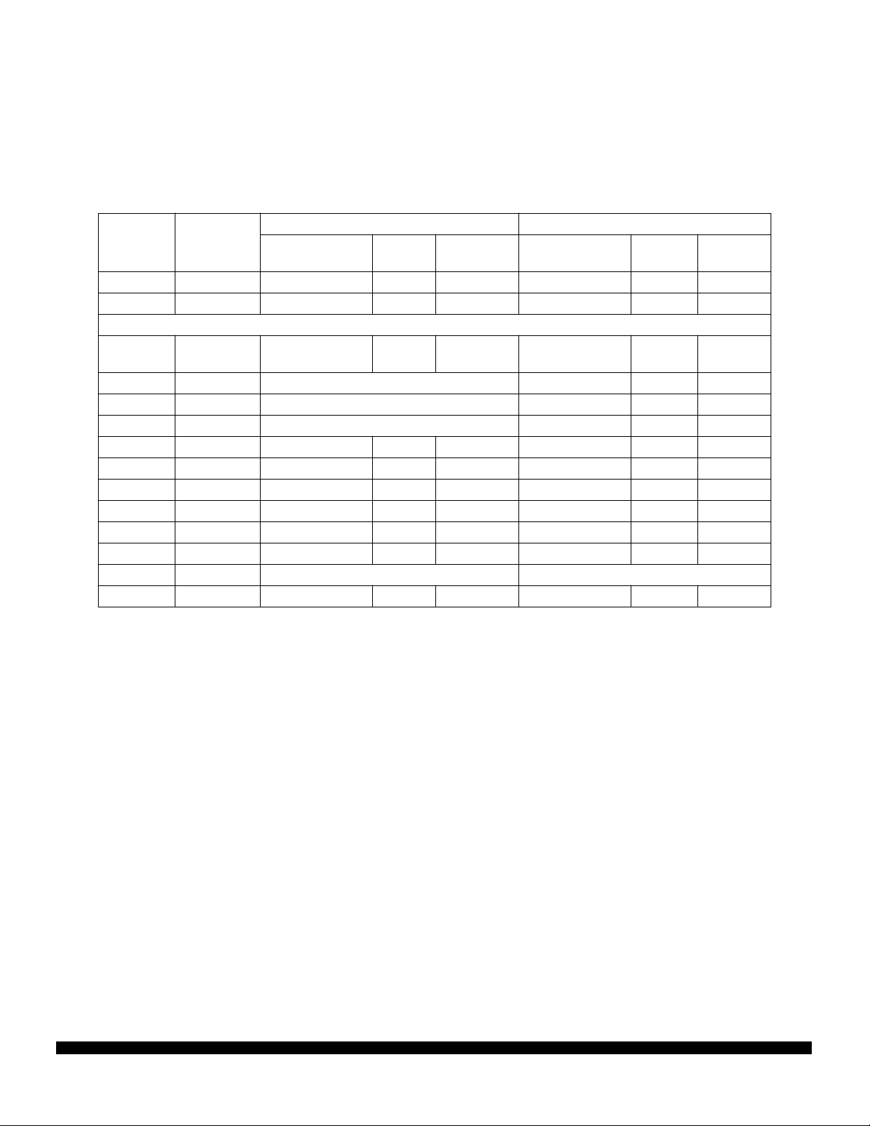
1.2 Ordering Information
The MC68HC912B32 is packaged in 80-pin quad flat pack (QFP) packaging and is shipped in two-piece
sample packs, 50-piece trays, or 250-piece bricks. Operating temperature range and voltage requirements are specified when ordering the MC68HC912B32 device. Refer to Table 1 for part numbers.
Table 1 MC68HC912B32 Device Ordering Information
Order Number
MC68HC912B32FU8 0 to + 70 ° C—
MC68HC912B32CFU8 − 40 to + 85 ° CC
MC68HC912B32VFU8 − 40 to + 105 ° CV
MC68HC912B32MFU8 − 40 to + 125 ° CM
MC68C912B32FU8 0 to + 70 ° C—
MC68C912B32CFU8 − 40 to + 85 ° CC
MC68B912B32FU8 0 to + 70 ° C — 2.7V–5.5V
NOTE: This part is also available in 2-piece sample packs and 250-piece bricks.
Temperature
Range Designator
Voltage Frequency Package
4.5V–5.5V
8 MHz
2.7V–3.6V
80-Pin QFP
Single Tray
50 Pcs
Evaluation boards, assemblers, compilers, and debuggers are available from Motorola and from thirdparty suppliers. An up-to-date list of products that support the M68HC12 family of microcontrollers can
be found on the World Wide Web at the following URL:
http://www.mcu.motsps.com
Documents to assist in product selection are available from the Motorola Literature Distribution Center
or your local Motorola Sales Office:
AMCU Device Selection Guide (SG166/D)
AMCU Software and Development Tool Selector Guide (SG176/D)
MOTOROLA MC68HC912B32
2 MC68HC912B32TS/D

1
6
9
25
32
37
47
52
57
TABLE OF CONTENTS
Section Page
1 Introduction
1.1 Features ......................................................................................................................................1
1.2 Ordering Information ...................................................................................................................2
1.3 MC68HC912B32 Block Diagram .................................................................................................5
2 Central Processing Unit
2.1 Programming Model ....................................................................................................................6
2.2 Data Types ..................................................................................................................................7
2.3 Addressing Modes .......................................................................................................................7
2.4 Indexed Addressing Modes .........................................................................................................8
2.5 Opcodes and Operands ..............................................................................................................8
3 Pinout and Signal Descriptions
3.1 MC68HC912B32 Pin Assignments .............................................................................................9
3.2 Power Supply Pins ....................................................................................................................10
3.3 Signal Descriptions ....................................................................................................................11
3.4 Port Signals ...............................................................................................................................15
3.5 Port Pull-Up, Pull-Down and Reduced Drive .............................................................................19
4 Register Block
5 Operating Modes and Resource Mapping
5.1 Operating Modes .......................................................................................................................25
5.2 Background Debug Mode ..........................................................................................................26
5.3 Internal Resource Mapping .......................................................................................................28
5.4 Memory Maps ............................................................................................................................31
6 Bus Control and Input/Output
6.1 Detecting Access Type from External Signals ..........................................................................32
6.2 Registers ...................................................................................................................................32
7 Flash EEPROM
7.1 Overview ...................................................................................................................................37
7.2 Flash EEPROM Control Block ...................................................................................................37
7.3 Flash EEPROM Array ...............................................................................................................37
7.4 Flash EEPROM Registers .........................................................................................................37
7.5 Operation ...................................................................................................................................40
7.6 Programming the Flash EEPROM ............................................................................................42
7.7 Erasing the Flash EEPROM ......................................................................................................44
7.8 Program/Erase Protection Interlocks .........................................................................................46
7.9 Stop or Wait Mode .....................................................................................................................46
7.10 Test Mode .................................................................................................................................46
8 EEPROM
8.1 EEPROM Programmer’s Model ................................................................................................47
8.2 EEPROM Control Registers ......................................................................................................48
9 Resets and Interrupts
9.1 Exception Priority ......................................................................................................................52
9.2 Maskable Interrupts ...................................................................................................................52
9.3 Interrupt Control and Priority Registers .....................................................................................53
9.4 Resets .......................................................................................................................................54
9.5 Effects of Reset .........................................................................................................................54
9.6 Register Stacking ......................................................................................................................55
10 Clock Functions
10.1 Clock Sources ...........................................................................................................................57
10.2 Computer Operating Properly (COP) ........................................................................................57
10.3 Real-Time Interrupt ...................................................................................................................57
10.4 Clock Monitor ............................................................................................................................57
10.5 Clock Function Registers ..........................................................................................................58
10.6 Clock Divider Chains .................................................................................................................60
20
MC68HC912B32 MOTOROLA
MC68HC912B32TS/D 3

63
73
83
98
TABLE OF CONTENTS (Continued)
Section Page
11 Pulse-Width Modulator
11.1 PWM Register Description ........................................................................................................65
11.2 PWM Boundary Cases ..............................................................................................................72
12 Standard Timer Module
12.1 Timer Registers .........................................................................................................................74
12.2 Timer Operation in Modes .........................................................................................................82
13 Serial Interface
13.1 Block Diagram ...........................................................................................................................83
13.2 Serial Communication Interface (SCI) .......................................................................................83
13.3 Serial Peripheral Interface (SPI) ................................................................................................90
13.4 Port S ........................................................................................................................................96
14 Byte Data Link Communications Module (BDLC)
14.1 Features ....................................................................................................................................98
14.2 BDLC Operating Modes ............................................................................................................98
14.3 Loopback Modes .......................................................................................................................99
14.4 BDLC Registers .........................................................................................................................99
14.5 J1850 Bus Errors .....................................................................................................................106
15 Analog-To-Digital Converter
15.1 Functional Description .............................................................................................................108
15.2 ATD Registers .........................................................................................................................108
15.3 ATD Mode Operation ..............................................................................................................114
16 Development Support
16.1 Instruction Queue ....................................................................................................................115
16.2 Background Debug Mode ........................................................................................................115
16.3 Breakpoints .............................................................................................................................123
16.4 Instruction Tagging ..................................................................................................................127
108
115
MOTOROLA MC68HC912B32
4 MC68HC912B32TS/D
1.3 MC68HC912B32 Block Diagram
V
BKGD
EXTAL
XTAL
RESET
PE0
PE1
PE2
PE3
PE4
PE5
PE6
PE7
V
FP
32-KBYTE FLASH EEPROM
1-KBYTE RAM
AN0
768-BYTE EEPROM
SMODN / TAGHI
SINGLE-WIRE
BACKGROUND
DEBUG MODULE
XIRQ
IRQ/V
R/W
LSTRB / TAGLO
PORT E
ECLK
IPIPE0 / MODA
IPIPE1 / MODB
DBE
CPU12
PERIODIC INTERRUPT
COP WATCHDOG
CLOCK MONITOR
PP
BREAK POINTS
LITE
INTEGRATION
MODULE
(LIM)
ATD
CONVERTER
TIMER AND
PULSE
ACCUMULATOR
SCI
I/O
SPI
AN1
AN2
AN3
AN4
AN5
AN6
AN7
IOC0
IOC1
IOC2
IOC3
OC7
IOC4
IOC5
IOC6
PAI
RxD
TxD
I/O
I/O
SDI/MISO
SDO/MOSI
SCK
CS/SS
RH
V
RL
V
DDA
V
SSA
DDRT
DDRS
PORT AD
PORT T
PORT S
V
RH
V
RL
V
DDA
V
SSA
PAD0
PAD1
PAD2
PAD3
PAD4
PAD5
PAD6
PAD7
PT0
PT1
PT2
PT3
PT4
PT5
PT6
PT7
PS0
PS1
PS2
PS3
PS4
PS5
PS6
PS7
WIDE
BUS
MULTIPLEXED ADDRESS/DATA BUS
DDRA
PORT A
PA4
PA7
PA6
PA5
ADDR15
ADDR14
ADDR13
ADDR12
DATA14
DATA13
DATA12
DATA15
DATA7
DATA6
DATA5
DATA4
NARROW BUS
PA3
PA2
ADDR11
ADDR10
DATA11
DATA10
DATA3
DATA2
PA1
PA0
ADDR9
ADDR8
DATA9
DATA8
DATA1
DATA0
PB7
PB6
ADDR7
ADDR6
DATA7
DATA6
DDRB
PORT B
PB5
ADDR5
DATA5
PB4
PB3
ADDR4
ADDR3
DATA4
DATA3
PB2
PB1
ADDR2
ADDR1
DATA2
DATA1
PB0
ADDR0
DATA0
PWM
I/O
BDLC
I/O
VDD × 2
× 2
V
SS
POWER FOR
INTERNAL
CIRCUITRY
PW0
PW1
PW2
PW3
I/O
I/O
I/O
I/O
DLCRx
DLCTx
I/O
I/O
I/O
I/O
I/O
V
× 2
DDX
V
× 2
SSX
POWER FOR
I/O DRIVERS
DDRP
PORT P
DDRDLC
PORT DLC
PP0
PP1
PP2
PP3
PP4
PP5
PP6
PP7
PDLC0
PDLC1
PDLC2
PDLC3
PDLC4
PDLC5
PDLC6
Figure 1 MC68HC912B32 Block Diagram
MC68HC912B32 MOTOROLA
MC68HC912B32TS/D 5

2 Central Processing Unit
The CPU12 is a high-speed, 16-bit processing unit. It has full 16-bit data paths and wider internal registers (up to 20 bits) for high-speed extended math instructions. The instruction set is a proper superset
of the M68HC11instruction set. The CPU12 allows instructions with odd byte counts, including many
single-byte instructions. This provides efficient use of ROM space. An instruction queue buffers program information so the CPU always has immediate access to at least three bytes of machine code at
the start of every instruction. The CPU12 also offers an extensive set of indexed addressing capabilities.
2.1 Programming Model
CPU12 registers are an integral part of the CPU and are not addressed as if they were memory locations.
15
15
15
15
15
7
AB
D
IX
IY
SP
PC
70
NSXHI ZVC
8-BIT ACCUMULATORS A & B
0
OR
16-BIT DOUBLE ACCUMULATOR D
0
INDEX REGISTER X
0
INDEX REGISTER Y
0
STACK POINTER
0
PROGRAM COUNTER
0
CONDITION CODE REGISTER
HC12 PROG MODEL
Figure 2 Programming Model
Accumulators A and B are general-purpose 8-bit accumulators used to hold operands and results of
arithmetic calculations or data manipulations. Some instructions treat the combination of these two 8bit accumulators as a 16-bit double accumulator (accumulator D).
Index registers X and Y are used for indexed addressing mode. In the indexed addressing mode, the
contents of a 16-bit index register are added to 5-bit, 9-bit, or 16-bit constants or the content of an accumulator to form the effective address of the operand to be used in the instruction.
Stack pointer (SP) points to the last stack location used. The CPU12 supports an automatic program
stack that is used to save system context during subroutine calls and interrupts, and can also be used
for temporary storage of data. The stack pointer can also be used in all indexed addressing modes.
Program counter is a 16-bit register that holds the address of the next instruction to be executed. The
program counter can be used in all indexed addressing modes except auto-increment/decrement.
Condition Code Register (CCR) contains five status indicators, two interrupt masking bits, and a
STOP disable bit. The five flags are half carry (H), negative (N), zero (Z), overflow (V), and carry/borrow
(C). The half-carry flag is used only for BCD arithmetic operations. The N, Z, V, and C status bits allow
for branching based on the results of a previous operation.
MOTOROLA MC68HC912B32
6 MC68HC912B32TS/D

2.2 Data Types
The CPU12 supports the following data types:
• Bit data
• 8-bit and 16-bit signed and unsigned integers
• 16-bit unsigned fractions
• 16-bit addresses
A byte is eight bits wide and can be accessed at any byte location. A word is composed of two consecutive bytes with the most significant byte at the lower value address. There are no special requirements
for alignment of instructions or operands.
2.3 Addressing Modes
Addressing modes determine how the CPU accesses memory locations to be operated upon. The
CPU12 includes all of the addressing modes of the M68HC11 CPU as well as several new forms of indexed addressing. Table 2 is a summary of the available addressing modes.
Table 2 M68HC12 Addressing Mode Summary
Addressing Mode Source Format Abbreviation Description
Inherent
Immediate
Direct INST
Extended INST
Relative
Indexed
(5-bit offset)
Indexed
(auto pre-decrement)
Indexed
(auto pre-increment)
Indexed
(auto post-
decrement)
Indexed
(auto post-increment)
Indexed
(accumulator offset)
Indexed
(9-bit offset)
Indexed
(16-bit offset)
Indexed-Indirect
(16-bit offset)
Indexed-Indirect
(D accumulator
offset)
(no externally supplied
operands)
INST #
INST #
INST
INST
INST
INST
INST
INST
INST
INST
INST
INST [
INST [D,
INST
opr8i
or
opr16i
opr8a
opr16a
rel8
INST
or
rel16
oprx5,xysp
oprx3,–xys
oprx3,+xys
oprx3,xys–
oprx3,xys+
abd,xysp
oprx9,xysp
oprx16,xysp
oprx16,xysp
xysp
INH Operands (if any) are in CPU registers
IMM
DIR
EXT Operand is a 16-bit address
REL
IDX 5-bit signed constant offset from x, y, sp, or pc
IDX Auto pre-decrement x, y, or sp by 1 ~ 8
IDX Auto pre-increment x, y, or sp by 1 ~ 8
IDX Auto post-decrement x, y, or sp by 1 ~ 8
IDX Auto post-increment x, y, or sp by 1 ~ 8
IDX
IDX1
IDX2
] [IDX2]
] [D,IDX]
Operand is included in instruction stream
8- or 16-bit size implied by context
Operand is the lower 8-bits of an address in the
range $0000 – $00FF
An 8-bit or 16-bit relative offset from the current
pc is supplied in the instruction
Indexed with 8-bit (A or B) or 16-bit (D) accumu-
lator offset from x, y, sp, or pc
9-bit signed constant offset from x, y, sp, or pc
(lower 8-bits of offset in one extension byte)
16-bit constant offset from x, y, sp, or pc
(16-bit offset in two extension bytes)
Pointer to operand is found at...
16-bit constant offset from x, y, sp, or pc
(16-bit offset in two extension bytes)
Pointer to operand is found at...
x, y, sp, or pc plus the value in D
MC68HC912B32 MOTOROLA
MC68HC912B32TS/D 7

2.4 Indexed Addressing Modes
The CPU12 indexed modes reduce execution time and eliminate code size penalties for using the Y
index register. CPU12 indexed addressing uses a postbyte plus zero, one, or two extension bytes after
the instruction opcode. The postbyte and extensions do the following tasks:
• Specify which index register is used
• Determine whether a value in an accumulator is used as an offset
• Enable automatic pre- or post-increment or decrement
• Specify use of 5-bit, 9-bit, or 16-bit signed offsets
Table 3 Summary of Indexed Operations
Postbyte
Code (xb)
Source Code
Syntax
rr0nnnnn ,r
n,r
−n,r
111rr0zs n,r
−n,r
111rr011 [n,r]
rr1pnnnn n,−r
n,+r
n,r−
n,r+
111rr1aa A,r
B,r
D,r
111rr111 [D,r]
Comments
rr; 00 = X, 01 = Y, 10 = SP, 11 = PC
5-bit constant offset n = –16 to +15
r can specify X, Y, SP, or PC
Constant offset (9- or 16-bit signed)
z- 0 = 9-bit with sign in LSB of postbyte(s) -256 < n < 255
1 = 16-bit 0 < n < 65,535
if z = s = 1, 16-bit offset indexed-indirect (see below)
r can specify X, Y, SP, or PC
16-bit offset indexed-indirect
rr can specify X, Y, SP, or PC 0 < n < 65,535
Auto pre-decrement/increment or Auto post-decrement/increment;
p = pre-(0) or post-(1), n = –8 to –1, +1 to +8
r can specify X, Y, or SP (PC not a valid choice)
+8 = 0111
…
+1 = 0000
-1 = 1111
…
-8 = 1000
Accumulator offset (unsigned 8-bit or 16-bit)
aa- 00 = A
01 = B
10 = D (16-bit)
11 = see accumulator D offset indexed-indirect
r can specify X, Y, SP, or PC
Accumulator D offset indexed-indirect
r can specify X, Y, SP, or PC
2.5 Opcodes and Operands
The CPU12 uses 8-bit opcodes. Each opcode identifies a particular instruction and associated addressing mode to the CPU. Several opcodes are required to provide each instruction with a range of addressing capabilities.
Only 256 opcodes would be available if the range of values were restricted to the number that can be
represented by 8-bit binary numbers. To expand the number of opcodes, a second page is added to the
opcode map. Opcodes on the second page are preceded by an additional byte with the value $18.
To provide additional addressing flexibility, opcodes can also be followed by a postbyte or extension
bytes. Postbytes implement certain forms of indexed addressing, transfers, exchanges, and loop primitives. Extension bytes contain additional program information such as addresses, offsets, and immediate data.
MOTOROLA MC68HC912B32
8 MC68HC912B32TS/D
3 Pinout and Signal Descriptions
3.1 MC68HC912B32 Pin Assignments
The MC68HC912B32 is available in a 80-pin quad flat pack (QFP). Most pins perform two or more functions, as described in the 3.3 Signal Descriptions. Figure 3 shows pin assignments. Shaded pins are
power and ground.
PORT P
PW3 / PP3
PW2 / PP2
PW1/ PP1
PW0/ PP0
IOC0 / PT0
IOC1 / PT1
PORT TPORT T
SMODN / T
ADDR0 / DATA0 / PB0
ADDR1 / DATA1 / PB1
ADDR2 / DATA2 / PB2
IOC2 / PT2
IOC3 / PT3
IOC4 / PT4
IOC5 / PT5
IOC6 / PT6
PAI / IOC7 / PT7
AGHI/ BKGD
PP5
PP4
V
V
/SS
PS6 / SCK
PS7 / CS
67
68
PORT S
PS2
PS3
PS4 / SDI/MISO
PS5 / SDO/MOSI
63
64
65
66
PS1 / TxD
62
PS0 / RxD
61
V
60
59
58
57
56
55
54
53
52
51
50
49
48
47
46
45
44
43
42
41
40
SSA
V
DDA
PAD7 / AN7
PAD6 / AN6
PAD5 / AN5
PAD4 / AN4
PAD3 / AN3
PAD2 / AN2
PAD1 / AN1
PAD0 / AN0
V
RL
V
RH
V
SS
V
DD
PA7 / DATA15 / ADDR15
PA6 / DATA14 / ADDR14
PA5 / DATA13 / ADDR13
PA4 / DATA12 / ADDR12
PA3 / DATA11 / ADDR11
PA2 / DATA10 / ADDR10
PORT AD
PORT DLC
SSX
DDX
V
PP7
79
V
77
78
PDLC3
PDLC2
PDLC1 / DLCTx
PDLC0 / DLCRx
73
74
75
76
MC68HC912B32
PDLC4
72
80-PIN QFP
PP6
80
1
2
3
4
5
6
7
8
9
10
DD
11
SS
12
13
14
15
16
17
18
19
20
21222324252627282930313233343536373839
PDLC6
PDLC5
70
71
FP
V
69
SSX
DDX
PORT B
ADDR4 / DATA4 / PB4
ADDR3 / DATA3 / PB3
ADDR6 / DATA6 / PB6
ADDR5 / DATA5 / PB5
/ PE7
DBE
MODB / IPIPE1 / PE6
ADDR7 / DATA7 / PB7
V
V
ECLK / PE4
MODA / IPIPE0 / PE5
EXTAL
RESET
XTAL
/ TAGLO / PE3
LSTRB
/ PE2
R/W
/ PE1
PP
/V
IRQ
/ PE0
XIRQ
PORT A*
ADDR9 / DATA9 / PA1
ADDR8 / DATA8 / PA0
HC12 80QFP
PORT EPORT E
* In narrow mode, high and low data bytes are multiplexed in alternate bus cycles on port A.
Figure 3 Pin Assignments for MC68HC912B32
MC68HC912B32 MOTOROLA
MC68HC912B32TS/D 9

3.2 Power Supply Pins
MC68HC912B32 power and ground pins are described below and summarized in Table 4.
3.2.1 Internal Power (VDD) and Ground (VSS)
Power is supplied to the MCU through V
and VSS. Because fast signal transitions place high, short-
DD
duration current demands on the power supply, use bypass capacitors with high-frequency characteristics and place them as close to the MCU as possible. Bypass requirements depend on how heavily
the MCU pins are loaded.
3.2.2 External Power (V
and Ground (V
DDX)
SSX
)
External power and ground for I/O drivers. Because fast signal transitions place high, short-duration current demands on the power supply, use bypass capacitors with high-frequency characteristics and
place them as close to the MCU as possible. Bypass requirements depend on how heavily the MCU
pins are loaded.
3.2.3 V
DDA
, V
SSA
Provides operating voltage and ground for the analog-to-digital converter. This allows the supply voltage to the A/D to be bypassed independently.
3.2.4 Analog-to-Digital Reference Voltages (VRH, VRL)
3.2.5 V
FP
Flash EEPROM programming voltage and supply voltage during normal operation.
3.2.6 V
PP
High voltage supply to EEPROM. Used to monitor charge pump output and testing. Not intended for
general applications use.
Table 4 MC68HC912B32 Power and Ground Connection Summary
Mnemonic Pin Number Description
V
V
V
V
V
V
V
V
V
V
DD
SS
DDX
SSX
DDA
SSA
RH
RL
FP
PP
10, 47
11, 48
31, 78
30, 77
59
60
49
50
69
37
Internal power and ground.
External power and ground, supply to pin drivers.
Operating voltage and ground for the analog-to-digital converter,
allows the supply voltage to the A/D to be bypassed independently.
Reference voltages for the analog-to-digital converter.
Programming voltage for the Flash EEPROM and required supply
for normal operation.
High voltage supply to EEPROM used for test purposes only in
special modes.
MOTOROLA MC68HC912B32
10 MC68HC912B32TS/D
3.3 Signal Descriptions
3.3.1 Crystal Driver and External Clock Input (XTAL, EXTAL)
These pins provide the interface for either a crystal or a CMOS compatible clock to control the internal
clock generator circuitry. Out of reset the frequency applied to EXTAL is twice the desired E-clock rate.
All the device clocks are derived from the EXTAL input frequency.
MCU
MCU
EXTAL
10 MΩ
XTAL
2 x E
CRYSTAL
Figure 4 Common Crystal Connections
EXTAL
XTAL
NC
CMOS-COMPATIBLE
EXTERNAL OSCILLATOR
C
C
COMMON XTAL CONN
2 x E
EXT EXTAL CONN
Figure 5 External Oscillator Connections
XTAL is the crystal output. The XTAL pin must be left unterminated when an external CMOS compatible
clock input is connected to the EXTAL pin. The XTAL output is normally intended to drive only a crystal.
The XTAL output can be buffered with a high-impedance buffer to drive the EXTAL input of another device.
In all cases take extra care in the circuit board layout around the oscillator pins. Load capacitances
shown in the oscillator circuits include all stray layout capacitances. Refer to Figure 4 and Figure 5 for
diagrams of oscillator circuits.
3.3.2 E-Clock Output (ECLK)
ECLK is the output connection for the internal bus clock and is used to demultiplex the address and data
and is used as a timing reference. ECLK frequency is equal to 1/2 the crystal frequency out of reset. Eclock output can be turned off in single-chip modes to reduce the effects of RFI. In special peripheral
mode the E clock is an input to the MCU. All clocks, including the E-clock, are halted when the MCU is
in STOP mode. It is possible to configure the MCU to interface to slow external memory. ECLK can be
stretched for such accesses.
MC68HC912B32 MOTOROLA
MC68HC912B32TS/D 11

3.3.3 Reset (RESET)
An active low bidirectional control signal, RESET, acts as an input to initialize the MCU to a known startup state. It also acts as an open-drain output to indicate that an internal failure has been detected in
either the clock monitor or COP watchdog circuit. The MCU goes into reset asynchronously and comes
out of reset synchronously. This allows the part to reach a proper reset state even if the clocks have
failed, while allowing synchronized operation when starting out of reset.
It is possible to determine whether a reset was caused by an internal source or an external source. An
internal source drives the pin low for 16 cycles; eight cycles later the pin is sampled. If the pin has returned high, either the COP watchdog vector or clock monitor vector will be taken. If the pin is still low,
the external reset is determined to be active and the reset vector is taken. Hold reset low for at least 32
cycles to assure that the reset vector is taken in the event that an internal COP watchdog time-out or
clock monitor fail occurs.
3.3.4 Maskable Interrupt Request (IRQ
)
The IRQ input provides a means of applying asynchronous interrupt requests to the MCU. Either falling
edge-sensitive triggering or level-sensitive triggering is program selectable (INTCR register). IRQ is always configured to level-sensitive triggering at reset. When the MCU is reset the IRQ function is
masked in the condition code register.
This pin is always an input and can always be read. In special modes it can be used to apply external
EEPROM V
and erase cycles. Because the IRQ
in support of EEPROM testing. External VPP is not needed for normal EEPROM program
PP
pin is also used as an EEPROM programming voltage pin, there is
an internal resistive pull-up on the pin.
3.3.5 Nonmaskable Interrupt (XIRQ)
The XIRQ input provides a means of requesting a nonmaskable interrupt after reset initialization. During
reset, the X bit in the condition code register (CCR) is set and any interrupt is masked until MCU software enables it. Because the XIRQ input is level sensitive, it can be connected to a multiple-source
wired-OR network. This pin is always an input and can always be read. There is an active pull-up on
this pin while in reset and immediately out of reset. The pull-up can be turned off by clearing PUPE in
the PUCR register. XIRQ is often used as a power loss detect interrupt.
Whenever XIRQ or IRQ are used with multiple interrupt sources (IRQ must be configured for level-sensitive operation if there is more than one source of IRQ interrupt), each source must drive the interrupt
input with an open-drain type of driver to avoid contention between outputs. There must also be an interlock mechanism at each interrupt source so that the source holds the interrupt line low until the MCU
recognizes and acknowledges the interrupt request. If the interrupt line is held low, the MCU will recognize another interrupt as soon as the interrupt mask bit in the MCU is cleared (normally upon return from
an interrupt).
3.3.6 Mode Select (SMODN, MODA, and MODB)
The state of these pins during reset determine the MCU operating mode. After reset, MODA and MODB
can be configured as instruction queue tracking signals IPIPE0 and IPIPE1. MODA and MODB have
active pulldowns during reset.
The SMODN pin can be used as BKGD or T
AGHI after reset.
3.3.7 Single-Wire Background Mode Pin (BKGD)
The BKGD pin receives and transmits serial background debugging commands. A special self-timing
protocol is used. The BKGD pin has an active pull-up when configured as input; BKGD has no pull-up
control. Refer to 16 Development Support.
MOTOROLA MC68HC912B32
12 MC68HC912B32TS/D

3.3.8 External Address and Data Buses (ADDR[15:0] and DATA[15:0])
External bus pins share function with general-purpose I/O ports A and B. In single-chip operating
modes, the pins can be used for I/O; in expanded modes, the pins are used for the external buses.
In expanded wide mode, ports A and B are used for multiplexed 16-bit data and address buses. PA[7:0]
correspond to ADDR[15:8]/DATA[15:8]; PB[7:0] correspond to ADDR[7:0]/DATA[7:0].
In expanded narrow mode, ports A and B are used for the 16-bit address bus, and an 8-bit data bus is
multiplexed with the most significant half of the address bus on port A. In this mode, 16-bit data is handled as two back-to-back bus cycles, one for the high byte followed by one for the low byte. PA[7:0]
correspond to ADDR[15:8] and to DATA[15:8] or DATA[7:0], depending on the bus cycle. The state of
the address pin should be latched at the rising edge of E. To allow for maximum address setup time at
external devices, a transparent latch should be used.
3.3.9 Read/Write (R/W
In all modes this pin can be used as I/O and is a general-purpose input with an active pull-up out of
reset. If the read/write function is required it should be enabled by setting the RDWE bit in the PEAR
register. External writes will not be possible until enabled.
3.3.10 Low-Byte Strobe (LSTRB)
In all modes this pin can be used as I/O and is a general-purpose input with an active pull-up out of
reset. If the strobe function is required, it should be enabled by setting the LSTRE bit in the PEAR register. This signal is used in write operations and so external low byte writes will not be possible until this
function is enabled. This pin is also used as TAGLO in special expanded modes and is multiplexed with
the LSTRB function.
3.3.11 Instruction Queue Tracking Signals (IPIPE1 and IPIPE0)
These signals are used to track the state of the internal instruction execution queue. Execution state is
time-multiplexed on the two signals. Refer to 16 Development Support.
3.3.12 Data Bus Enable (DBE)
The DBE pin (PE7) is an active low signal that will be asserted low during E-clock high time. DBE provides separation between output of a multiplexed address and the input of data. When an external address is stretched, DBE is asserted during what would be the last quarter cycle of the last E-clock cycle
of stretch. In expanded modes this pin is used to enable the drive control of external buses during external reads. Use of the DBE is controlled by the NDBE bit in the PEAR register. DBE is enabled out of
reset in expanded modes. This pin has an active pull-up during and after reset in single-chip modes.
)
MC68HC912B32 MOTOROLA
MC68HC912B32TS/D 13
Table 5 MC68HC912B32 Signal Description Summary
Pin Name Pin Number Description
PW[3:0] 3–6 Pulse Width Modulator channel outputs.
ADDR[7:0]
DATA[7:0]
ADDR[15:8]
DATA[15:8]
IOC[7:0] 16–12, 9–7
PAI 16 Pulse accumulator input
AN[7:0] 58–51 Analog inputs for the analog-to-digital conversion module
DBE
MODB, MODA 27, 28 State of mode select pins during reset determine the initial operating mode of the
IPIPE1, IPIPE0 27, 28
ECLK 29
RESET 32
EXTAL 33
XTAL 34
LSTRB
AGLO 35 Pin used in instruction tagging. See 16 Development Support.
T
R/W
IRQ 37
XIRQ 38
BKGD 17
AGHI 17 Pin used in instruction tagging. See 16 Development Support.
T
DLCRx 76 BDLC receive pin
DLCTx 75 BDLC transmit pin
/SS 68 Slave select output for SPI master mode, input for slave mode or master mode.
CS
SCK 67 Serial clock for SPI system.
SDO/MOSI 66 Master out/slave in pin for serial peripheral interface
SDI/MISO 65 Master in/slave out pin for serial peripheral interface
TxD0 62 SCI transmit pin
RxD0 61 SCI receive pin
25–18
46–39
26
35
36
External bus pins share function with general-purpose I/O ports A and B. In single chip modes, the pins can be used for I/O. In expanded modes, the pins are
used for the external buses.
Pins used for input capture and output compare in the timer and pulse accumulator subsystem.
Data bus control and, in expanded mode, enables the drive control of external
buses during external reads.
MCU. After reset, MODB and MODA can be configured as instruction queue
tracking signals IPIPE1 and IPIPE0 or as general-purpose I/O pins.
E-clock is the output connection for the external bus clock. ECLK is used as a
timing reference and for address demultiplexing.
An active low bidirectional control signal, RESET
MCU to a known start-up state, and an output when COP or clock monitor causes
a reset.
Crystal driver and external clock input pins. On reset all the device clocks are derived from the EXTAL input frequency. XTAL is the crystal output.
Low byte strobe (0 = low byte valid), in all modes this pin can be used as I/O. The
low strobe function is the exclusive-NOR of A0 and the internal SZ8 signal. (The
SZ8
internal signal indicates the size 16/8 access.)
Indicates direction of data on expansion bus. Shares function with general-purpose I/O. Read/write in expanded modes.
Maskable interrupt request input provides a means of applying asynchronous interrupt requests to the MCU. Either falling edge-sensitive triggering or level-sensitive triggering is program selectable (INTCR register).
Provides a means of requesting asynchronous non-maskable interrupt requests
after reset initialization.
Single-wire background interface pin is dedicated to the background debug function. During reset, this pin determines special or normal operating mode.
acts as an input to initialize the
MOTOROLA MC68HC912B32
14 MC68HC912B32TS/D

3.4 Port Signals
The MC68HC912B32 incorporates eight ports which are used to control and access the various device
subsystems. When not used for these purposes, port pins may be used for general-purpose I/O. In addition to the pins described below, each port consists of a data register which can be read and written
at any time, and, with the exception of port AD and PE[1:0], a data direction register which controls the
direction of each pin. After reset all port pins are configured as input.
3.4.1 Port A
Port A pins are used for address and data in expanded modes. The port data register is not in the address map during expanded and peripheral mode operation. When it is in the map, port A can be read
or written at anytime.
Register DDRA determines whether each port A pin is an input or output. DDRA is not in the address
map during expanded and peripheral mode operation. Setting a bit in DDRA makes the corresponding
bit in port A an output; clearing a bit in DDRA makes the corresponding bit in port A an input. The default
reset state of DDRA is all zeros.
When the PUPA bit in the PUCR register is set, all port A input pins are pulled up internally by an active
pull-up device. This bit has no effect if the port is being used in expanded modes as the pull-ups are
inactive.
Setting the RDPA bit in register RDRIV causes all port A outputs to have reduced drive level. RDRIV
can be written once after reset. RDRIV is not in the address map in peripheral mode. Refer to 6 Bus
Control and Input/Output.
3.4.2 Port B
Port B pins are used for address and data in expanded modes. The port data register is not in the address map during expanded and peripheral mode operation. When it is in the map, port B can be read
or written at anytime.
Register DDRB determines whether each port B pin is an input or output. DDRB is not in the address
map during expanded and peripheral mode operation. Setting a bit in DDRB makes the corresponding
bit in port B an output; clearing a bit in DDRB makes the corresponding bit in port B an input. The default
reset state of DDRB is all zeros.
When the PUPB bit in the PUCR register is set, all port B input pins are pulled up internally by an active
pull-up device. This bit has no effect if the port is being used in expanded modes as the pull-ups are
inactive.
Setting the RDPB bit in register RDRIV causes all port B outputs to have reduced drive level. RDRIV
can be written once after reset. RDRIV is not in the address map in peripheral mode. Refer to 6 Bus
Control and Input/Output.
3.4.3 Port E
Port E pins operate differently from port A and B pins. Port E pins are used for bus control signals and
interrupt service request signals. When a pin is not used for one of these specific functions, it can be
used as general-purpose I/O. However, two of the pins (PE[1:0]) can only be used for input, and the
states of these pins can be read in the port data register even when they are used for IRQ
The PEAR register determines pin function, and register DDRE determines whether each pin is an input
or output when it is used for general-purpose I/O. PEAR settings override DDRE settings. Because
PE[1:0] are input-only pins, only DDRE[7:2] have effect. Setting a bit in the DDRE register makes the
corresponding bit in port E an output; clearing a bit in the DDRE register makes the corresponding bit
in port E an input. The default reset state of DDRE is all zeros.
and XIRQ.
MC68HC912B32 MOTOROLA
MC68HC912B32TS/D 15

When the PUPE bit in the PUCR register is set, PE[7,3,2,0] are pulled up. PE[7,3,2,0] are pulled up active devices, while PE1 is always pulled up by means of an internal resistor.
Neither port E nor DDRE is in the map in peripheral mode; neither is in the internal map in expanded
modes with EME set.
Setting the RDPE bit in register RDRIV causes all port E outputs to have reduced drive level. RDRIV
can be written once after reset. RDRIV is not in the address map in peripheral mode. Refer to 6 Bus
Control and Input/Output.
3.4.4 Port DLC
BDLC pins can be configured as general-purpose I/O port DLC. When BDLC functions are not enabled,
the port has seven general-purpose I/O pins, PDLC[6:0]. The DLCSCR register controls port DLC function. The BDLC function, enabled with the BDLCEN bit, takes precedence over other port functions.
Register DDRDLC determines whether each port DLC pin is an input or output. Setting a bit in DDRDLC
makes the corresponding pin in port DLC an output; clearing a bit makes the corresponding pin an input.
After reset port DLC pins are configured as inputs.
When the PUPDLC bit in the DLCSCR register is set, all port DLC input pins are pulled up internally by
an active pull-up device.
Setting the RDPDLC bit in register DLCSCR causes all port DLC outputs to have reduced drive level.
Levels are at normal drive capability after reset. RDPDLC can be written anytime after reset. Refer to
14 Byte Data Link Communications Module (BDLC).
3.4.5 Port AD
Input to the analog-to-digital subsystem and general-purpose input. When analog-to-digital functions
are not enabled, the port has eight general-purpose input pins, P AD[7:0]. The ADPU bit in the ATDCTL2
register enables the A/D function.
Port AD pins are inputs; no data direction register is associated with this port. The port has no resistive
input loads and no reduced drive controls. Refer to 15 Analog-To-Digital Converter.
3.4.6 Port P
The four pulse-width modulation channel outputs share general-purpose port P pins. The PWM function
is enabled with the PWEN register. Enabling PWM pins takes precedence over the general-purpose
port. When pulse-width modulation is not in use, the port pins may be used for general-purpose I/O.
Register DDRP determines pin direction of port P when used for general-purpose I/O. When DDRP bits
are set, the corresponding pin is configured for output. On reset the DDRP bits are cleared and the corresponding pin is configured for input.
When the PUPP bit in the PWCTL register is set, all input pins are pulled up internally by an active pullup device. Pull-ups are disabled after reset.
Setting the RDPP bit in the PWCTL register configures all port P outputs to have reduced drive levels.
Levels are at normal drive capability after reset. The PWCTL register can be read or written anytime
after reset. Refer to 11 Pulse-Width Modulator.
3.4.7 Port T
This port provides eight general-purpose I/O pins when not enabled for input capture and output compare in the timer and pulse accumulator subsystem. The TEN bit in the TSCR register enab les the timer
function. The pulse accumulator subsystem is enabled with the PAEN bit in the PACTL register.
MOTOROLA MC68HC912B32
16 MC68HC912B32TS/D

Register DDRT determines pin direction of port T when used for general-purpose I/O. When DDRT bits
are set, the corresponding pin is configured for output. On reset the DDRT bits are cleared and the corresponding pin is configured for input.
When the PUPT bit in the TMSK2 register is set, all input pins are pulled up internally by an active pullup device. Pull-ups are disabled after reset.
Setting the RDPT bit in the TMSK2 register configures all port T outputs to have reduced drive levels.
Levels are at normal drive capability after reset. The TMSK2 register can be read or written anytime
after reset. Refer to 12 Standard Timer Module.
3.4.8 Port S
Port S is the 8-bit interface to the standard serial interface consisting of the serial communications interface (SCI) and serial peripheral interface (SPI) subsystems. Port S pins are available for general-purpose parallel I/O when standard serial functions are not enabled.
Port S pins serve several functions depending on the various internal control registers. If WOMS bit in
the SC0CR1 register is set, the P-channel drivers of the output buffers are disabled for bits 0 through 1
(2 through 3). If SWOM bit in the SP0CR1 register is set, the P-channel drivers of the output buffers are
disabled for bits 4 through 7. (wired-OR mode). The open drain control effects both the serial and the
general-purpose outputs. If the RDPSx bits in the PURDS register are set, the appropriate port S pin
drive capabilities are reduced. If PUPSx bits in the PURDS register are set, the appropriate pull-up device is connected to each port S pin which is programmed as a general-purpose input . If the pin is programmed as a general-purpose output, the pull-up is disconnected from the pin regardless of the state
of the individual PUPSx bits. See 13 Serial Interface.
MC68HC912B32 MOTOROLA
MC68HC912B32TS/D 17

Table 6 MC68HC912B32 Port Description Summary
Port Name
Port A
PA[7:0]
Port B
PB[7:0]
Port AD
PAD[7:0]
Port DLC
PDLC[6:0]
Port E
PE[7:0]
Port P
PP[7:0]
Port S
PS[7:0]
Port T
PT[7:0]
Pin
Numbers
46–39
25–18
58–51 In Analog-to-digital converter and general-purpose I/O.
70–76
26–29, 35–38
79, 80, 1–6
68–61
16–12, 9–7
Data Direction
DD Register (Address) Description
In/Out
DDRA ($0002)
In/Out
DDRB ($0003)
In/Out
DDRDLC ($00FF)
PE[1:0] In
PE[7:2] In/Out
DDRE ($0009)
In/Out
DDRP ($0057)
In/Out
DDRS ($00D7)
In/Out
DDRT ($00AF)
Port A and port B pins are used for address and data in expanded modes. The port data registers are not in the address
map during expanded and peripheral mode operation. When
in the map, port A and port B can be read or written any time.
DDRA and DDRB are not in the address map in expanded or
peripheral modes.
Byte Data Link Communication (BDLC) subsystem and
general-purpose I/O.
Mode selection, bus control signals and interrupt service
request signals; or general-purpose I/O.
General-purpose I/O. PP[3:0] are use with the pulse-width
modulator when enabled.
Serial communications interface and serial peripheral interface subsystems and general-purpose I/O.
General-purpose I/O when not enabled for input capture and
output compare in the timer and pulse accumulator subsystem.
MOTOROLA MC68HC912B32
18 MC68HC912B32TS/D
3.5 Port Pull-Up, Pull-Down and Reduced Drive
MCU ports can be configured for internal pull-up. To reduce power consumption and RFI, the pin output
drivers can be configured to operate at a reduced drive level. Reduced drive causes a slight increase
in transition time depending on loading and should be used only for ports which have a light loading.
Table 7 summarizes the port pull-up default status and controls.
Table 7 Port Pull-Up, Pull-Down and Reduced Drive Summary
Enable Bit Reduced Drive Control Bit
Port
Name
Port A Pull-up PUCR ($000C) PUPA Disabled RDRIV ($000D) RDPA Full Drive
Port B Pull-up PUCR ($000C) PUPB Disabled RDRIV ($000D) RDPB Full Drive
Port E:
PE7, PE3,
PE2, PE0
PE1 Pull-up Always Enabled RDRIV ($000D) RDPE Full Drive
PE[6:4] None — RDRIV ($000D) RDPE Full Drive
PE[6:5] Pull-down Enabled During Reset — — —
Port P Pull-up PWCTL ($0054) PUPP Disabled PWCTL ($0054) RDPP Full Drive
Port S Pull-up PURDS ($00DB) PUPS0 Disabled PURDS ($00DB) RDPS0 Full Drive
PS[3:2] Pull-up PURDS ($00DB) PUPS1 Disabled PURDS ($00DB) RDPS1 Full Drive
PS[7:4] Pull-up PURDS ($00DB) PUPS2 Disabled PURDS ($00DB) RDPS2 Full Drive
Port T Pull-up TMSK2 ($008D) PUPT Disabled TMSK2 ($008D) RDPT Full Drive
Port DLC Pull-up DLCSCR ($00FD) DLCPUE Disabled DLCSCR ($00FD) DLCRDV Full Drive
Port AD None — —
BKGD Pull-up — — Enabled — — Full Drive
Resistive
Input Loads
Pull-up PUCR ($000C) PUPE Enabled RDRIV ($000D) RDPE Full Drive
Register
(Address)
Bit Name Reset State
Register
(Address)
Bit Name
Reset
State
MC68HC912B32 MOTOROLA
MC68HC912B32TS/D 19

4 Register Block
The register block can be mapped to any 2-Kbyte boundary within the standard 64-Kbyte address space
by manipulating bits REG[15:11] in the INITRG register. INITRG establishes the upper five bits of the
register block’s 16-bit address. The register block occupies the first 512 bytes of the 2-Kbyte block. Default addressing (after reset) is indicated in the table below. For additional information refer to 5 Oper-
ating Modes and Resource Mapping.
Table 8 MC68HC912B32 Register Map (Sheet 1 of 5)
Address Bit 7 65432 1Bit 0 Name
$0000 PA7 PA6 PA5 PA4 PA3 PA2 PA1 PA0 PORTA
$0001 PB7 PB6 PB5 PB4 PB3 PB2 PB1 PB0
$0002 DDA7 DDA6 DDA5 DDA4 DDA3 DDA2 DDA1 DDA0
$0003 DDB7 DDB6 DDB5 DDB4 DDB3 DDB2 DDB1 DDB0
$0004 000000 00Reserved
$0005 000000 00Reserved
$0006 000000 00Reserved
$0007 000000 00Reserved
$0008 PE7 PE6 PE5 PE4 PE3 PE2 PE1 PE0 PORTE
$0009 DDE7 DDE6 DDE5 DDE4 DDE3 DDE2 0 0
$000A NDBE 0 PIPOE NECLK LSTRE RDWE 0 0
$000B SMODN MODB MODA ESTR IVIS EBSWAI 0 EME MODE
$000C 0 0 0 PUPE 0 0 PUPB PUPA
$000D 0000RDPE 0 RDPB RDPA
$000E 000000 0 0Reserved
$000F 000000 0 0Reserved
$0010 RAM15 RAM14 RAM13 RAM12 RAM11 0 0 0 INITRM
$0011 REG15 REG14 REG13 REG12 REG11 0 0 MMSWAI INITRG
$0012 EE15 EE14 EE13 EE12 0 0 0 EEON INITEE
$0013 0 NDRF RFSTR1 RFSTR0 EXSTR1 EXSTR0 MAPROM ROMON MISC
$0014 RTIE RSWAI RSBCK 0 RTBYP RTR2 RTR1 RTR0 RTICTL
$0015 RTIF 000000 0RTIFLG
$0016 CME FCME FCM FCOP DISR CR2 CR1 CR0 COPCTL
$0017 Bit 7 654321Bit 0 COPRST
$0018 ITE6 ITE8 ITEA ITEC ITEE ITF0 ITF2 ITF4 ITST0
$0019 ITD6 ITD8 ITDA ITDC ITDE ITE0 ITE2 ITE4 ITST1
$001A ITC6 ITC8 ITCA ITCC ITCE ITD0 ITD2 ITD4 ITST2
$001B 00000ITC0 ITC2 ITC4 ITST3
$001C–
$001D
000000 0 0Reserved
$001E IRQE IRQEN DLY 0 0 0 0 0 INTCR
$001F 1 1 PSEL5 PSEL4 PSEL3 PSEL2 PSEL1 0 HPRIO
$0020 BKEN1 BKEN0 BKPM 0 BK1ALE BK0ALE 0 0 BRKCT0
$0021 0 BKDBE BKMBH BKMBL BK1RWE BK1RW BK0RWE BK0RW BRKCT1
$0022 Bit 15 14 13 12 11 10 9 Bit 8 BRKAH
PORTB
DDRA
DDRB
DDRE
PEAR
PUCR
RDRIV
1
1
1
1
2
2
2
3
3
3
MOTOROLA MC68HC912B32
20 MC68HC912B32TS/D

Table 8 MC68HC912B32 Register Map (Sheet 2 of 5)
Address Bit 7 65432 1Bit 0 Name
$0023 Bit 7 654321Bit 0 BRKAL
$0024 Bit 15 14 13 12 11 10 9 Bit 8 BRKDH
$0025 Bit 7 654321Bit 0 BRKDL
$0026–
$003F
$0040 CON23 CON01 PCKA2 PCKA1 PCKA0 PCKB2 PCKB1 PCKB0 PWCLK
$0041 PCLK3 PCLK2 PCLK1 PCLK0 PPOL3 PPOL2 PPOL1 PPOL0 PWPOL
$0042 0000PWEN3 PWEN2 PWEN1 PWEN0 PWEN
$0043 Bit 7 654321Bit 0 PWPRES
$0044 Bit 7 654321Bit 0 PWSCAL0
$0045 Bit 7 654321Bit 0 PWSCNT0
$0046 Bit 7 654321Bit 0 PWSCAL1
$0047 Bit 7 654321Bit 0 PWSCNT1
$0048 Bit 7 654321Bit 0 PWCNT0
$0049 Bit 7 654321Bit 0 PWCNT1
$004A Bit 7 65432 1Bit 0 PWCNT2
$004B Bit 7 65432 1Bit 0 PWCNT3
$004C Bit 7 65432 1Bit 0 PWPER0
$004D Bit 7 65432 1Bit 0 PWPER1
$004E Bit 7 65432 1Bit 0 PWPER2
$004F Bit 7 65432 1Bit 0 PWPER3
$0050 Bit 7 654321Bit 0 PWDTY0
$0051 Bit 7 654321Bit 0 PWDTY1
$0052 Bit 7 654321Bit 0 PWDTY2
$0053 Bit 7 654321Bit 0 PWDTY3
$0054 0 0 0 PSWAI CENTR RDPP PUPP PSBCK PWCTL
$0055 DISCR DISCP DISCAL 0 0 0 0 0 PWTST
$0056 PP7 PP6 PP5 PP4 PP3 PP2 PP1 PP0 PORTP
$0057 DDP7 DDP6 DDP5 DDP4 DDP3 DDP2 DDP1 DDP0 DDRP
$0058–
$005F
$0060 000000 0 0ATDCTL0
$0061 000000 0 0ATDCTL1
$0062 ADPU AFFC ASWAI 0 0 0 ASCIE ASCIF ATDCTL2
$0063 000000FRZ1 FRZ0 ATDCTL3
$0064 0 SMP1 SMP0 PRS4 PRS3 PRS2 PRS1 PRS0 ATDCTL4
$0065 0 S8CM SCAN MULT CD CC CB CA ATDCTL5
$0066 SCF 0000CC2CC1CC0ATDSTAT
$0067 CCF7 CCF6 CCF5 CCF4 CCF3 CCF2 CCF1 CCF0 ATDSTAT
$0068 SAR9 SAR8 SAR7 SAR6 SAR5 SAR4 SAR3 SAR2 ATDTSTH
$0069 SAR1 SAR0 RST TSTOUT TST3 TST2 TST1 TST0 ATDTSTL
$006A–
$006E
000000 0 0Reserved
000000 0 0Reserved
000000 0 0Reserved
MC68HC912B32 MOTOROLA
MC68HC912B32TS/D 21

Table 8 MC68HC912B32 Register Map (Sheet 3 of 5)
Address Bit 7 65432 1Bit 0 Name
$006F PAD7 PAD6 PAD5 PAD4 PAD3 PAD2 PAD1 PAD0 PORTAD
$0070 Bit 7 654321Bit 0 ADR0H
$0071 000000 0 0Reserved
$0072 Bit 7 654321Bit 0 ADR1H
$0073 000000 0 0Reserved
$0074 Bit 7 654321Bit 0 ADR2H
$0075 000000 0 0Reserved
$0076 Bit 7 654321Bit 0 ADR3H
$0077 000000 0 0Reserved
$0078 Bit 7 654321Bit 0 ADR4H
$0079 000000 0 0Reserved
$007A Bit 7 65432 1Bit 0 ADR5H
$007B 000000 0 0Reserved
$007C Bit 7 65432 1Bit 0 ADR6H
$007D 000000 0 0Reserved
$007E Bit 7 65432 1Bit 0 ADR7H
$007F 000000 0 0Reserved
$0080 IOS7 IOS6 IOS5 IOS4 IOS3 IOS2 IOS1 IOS0 TIOS
$0081 FOC7 FOC6 FOC5 FOC4 FOC3 FOC2 FOC1 FOC0 CFORC
$0082 OC7M7 OC7M6 OC7M5 OC7M4 OC7M3 OC7M2 OC7M1 OC7M0 OC7M
$0083 OC7D7 OC7D6 OC7D5 OC7D4 OC7D3 OC7D2 OC7D1 OC7D0 OC7D
$0084 Bit 15 14 13 12 11 10 9 Bit 8 TCNT (H)
$0085 Bit 7 654321Bit 0 TCNT (L)
$0086 TEN TSWAI TSBCK TFFCA 0 0 0 0 TSCR
$0087 000000 0 0TQCR
$0088 OM7 OL7 OM6 OL6 OM5 OL5 OM4 OL4 TCTL1
$0089 OM3 OL3 OM2 OL2 OM1 OL1 OM0 OL0 TCTL2
$008A EDG7B EDG7A EDG6B EDG6A EDG5B EDG5A EDG4B EDG4A TCTL3
$008B EDG3B EDG3A EDG2B EDG2A EDG1B EDG1A EDG0B EDG0A TCTL4
$008C C7I C6I C5I C4I C3I C2I C1I C0I TMSK1
$008D TOI 0 PUPT RDPT TCRE PR2 PR1 PR0 TMSK2
$008E C7F C6F C5F C4F C3F C2F C1F C0F TFLG1
$008F TOF 00000 0 0TFLG2
$0090 Bit 15 14 13 12 11 10 9 Bit 8 TC0 (H)
$0091 Bit 7 654321Bit 0 TC0 (L)
$0092 Bit 15 14 13 12 11 10 9 Bit 8 TC1 (H)
$0093 Bit 7 654321Bit 0 TC1 (L)
$0094 Bit 15 14 13 12 11 10 9 Bit 8 TC2 (H)
$0095 Bit 7 654321Bit 0 TC2 (L)
$0096 Bit 15 14 13 12 11 10 9 Bit 8 TC3 (H)
$0097 Bit 7 654321Bit 0 TC3 (L)
$0098 Bit 15 14 13 12 11 10 9 Bit 8 TC4 (H)
MOTOROLA MC68HC912B32
22 MC68HC912B32TS/D

Table 8 MC68HC912B32 Register Map (Sheet 4 of 5)
Address Bit 7 65432 1Bit 0 Name
$0099 Bit 7 654321Bit 0 TC4 (L)
$009A Bit 15 14 13 12 11 10 9 Bit 8 TC5 (H)
$009B Bit 7 65432 1Bit 0 TC5 (L)
$009C Bit 15 14 13 12 11 10 9 Bit 8 TC6 (H)
$009D Bit 7 65432 1Bit 0 TC6 (L)
$009E Bit 15 14 13 12 11 10 9 Bit 8 TC7 (H)
$009F Bit 7 65432 1Bit 0 TC7 (L)
$00A0 0 PAEN PAMOD PEDGE CLK1 CLK0 PAOVI PAI PACTL
$00A1 000000PAOVF PAIF PAFLG
$00A2 Bit 15 14 13 12 11 10 9 Bit 8 PACNT
$00A3 Bit 7 65432 1Bit 0 PACNT
$00A4–
$00AC
$00AD 000000TCBYP PCBYP TIMTST
$00AE PT7 PT6 PT5 PT4 PT3 PT2 PT1 PT0 PORTT
$00AF DDT7 DDT6 DDT5 DDT4 DDT3 DDT2 DDT1 DDT0 DDRT
$00B0–
$00BF
$00C0 BTST BSPL BRLD SBR12 SBR11 SBR10 SBR9 SBR8 SC0BDH
$00C1 SBR7 SBR6 SBR5 SBR4 SBR3 SBR2 SBR1 SBR0 SC0BDL
$00C2 LOOPS WOMS RSRC M WAKE ILT PE PT SC0CR1
$00C3 TIE TCIE RIE ILIE TE RE RWU SBK SC0CR2
$00C4 TDRE TC RDRF IDLE OR NF FE PF SC0SR1
$00C5 000000 0RAFSC0SR2
$00C6 R8 T8 0 0 0 0 0 0 SC0DRH
$00C7 R7/T7 R6/T6 R5/T5 R4/T4 R3/T3 R2/T2 R1/T1 R0/T0 SC0DRL
$00C8–
$00CF
$00D0 SPIE SPE SWOM MSTR CPOL CPHA SSOE LSBF SP0CR1
$00D1 000000SSWAI SPC0 SP0CR2
$00D2 00000SPR2 SPR1 SPR0 SP0BR
$00D3 SPIF WCOL 0 MODF 0 0 0 0 SP0SR
$00D4 000000 0
$00D5 Bit 7 65432 1Bit 0 SP0DR
$00D6 PS7 PS6 PS5 PS4 PS3 PS2 PS1 PS0 PORTS
$00D7 DDS7 DDS6 DDS5 DDS4 DDS3 DDS2 DDS1 DDS0 DDRS
$00D8–
$00DA
$00DB 0 RDPS2 RDPS1 RDPS0 0 PUPS2 PUPS1 PUPS0 PURDS
$00DC–
$00EF
$00F0 11111EESWAI PROTLCK EERC EEMCR
$00F1 1 1 1 BPROT4 BPROT3 BPROT2 BPROT1 BPROT0 EEPROT
000000 0 0Reserved
000000 0 0Reserved
000000 0 0Reserved
0 Reserved
000000 0 0Reserved
000000 0 0
Reserved
MC68HC912B32 MOTOROLA
MC68HC912B32TS/D 23

Table 8 MC68HC912B32 Register Map (Sheet 5 of 5)
Address Bit 7 65432 1Bit 0 Name
$00F2 EEODD EEVEN MARG EECPD EECPRD 0 EECPM 0 EETST
$00F3 BULKP 0 0 BYTE ROW ERASE EELAT EEPGM EEPROG
$00F4 000000 0LOCK FEELCK
$00F5 000000 0BOOTP FEEMCR
$00F6 FSTE GADR HVT FENLV FDISVFP VTCK STRE MWPR FEETST
$00F7 0 0 0 FEESWAI SVFP ERAS LAT ENPE FEECTL
$00F8 IMSG CLKS R1 R0 0 0 IE WCM BCR1
$00F9 0 0 I3 I2 I1 I0 0 0 BSVR
$00FA ALOOP DLOOP RX4XE NBFS TEOD TSIFR TMIFR1 TMIFR0 BCR2
$00FB D7 D6 D5 D4 D3 D2 D1 D0 BDR
$00FC ATE RXPOL 0 0 BO3 BO2 BO1 BO0 BARD
$00FD 00000BDLCEN DLCPUE DLCRDV DLCSCR
$00FE 0 PDLC6 PDLC5 PDLC4 PDLC3 PDLC2 PDLC1 PDLC0 PORTDLC
$00FF 0 DDDLC6 DDDLC5 DDDLC4 DDDLC3 DDDLC2 DDDLC1 DDDLC0 DDRDLC
$0100–
$01FF
NOTES:
1. Port A, port B, and data direction registers DDRA and DDRB are not in map in expanded and peripheral modes.
2. Port E and DDRE not in map in peripheral mode; also not in map in expanded modes with EME set.
3. Not in map in peripheral mode.
000000 0 0Reserved
MOTOROLA MC68HC912B32
24 MC68HC912B32TS/D

5 Operating Modes and Resource Mapping
Eight possible operating modes determine the operating configuration of the MC68HC912B32. Each
mode has an associated default memory map and external bus configuration. After reset, most system
resources can be mapped to other addresses by writing to the appropriate control registers.
5.1 Operating Modes
The operating mode out of reset is determined by the states of the BKGD, MODB, and MODA pins during reset.
The SMODN, MODB, and MODA bits in the MODE register show current operating mode and provide
limited mode switching during operation. The states of the BKGD, MODB, and MODA pins are latched
into these bits on the rising edge of the reset signal. During reset an active pull-up is connected to the
BKGD pin (as input) and active pulldowns are connected to the MODB and MODA pins. If an open occurs on any of these pins, the device will operate in normal single-chip mode.
Table 9 Mode Selection
BKGD MODB MODA Mode Port A Port B
0 0 0 Special Single Chip General-Purpose I/O General-Purpose I/O
0 0 1 Special Expanded Narrow ADDR[15:8]/DATA[15:0] ADDR[7:0]
0 1 0 Special Peripheral ADDR/DATA ADDR/DATA
0 1 1 Special Expanded Wide ADDR/DATA ADDR/DATA
1 0 0 Normal Single Chip General-Purpose I/O General-Purpose I/O
1 0 1 Normal Expanded Narrow ADDR[15:8]/DATA[15:0] ADDR[7:0]
1 1 0 Reserved (Forced to Peripheral) — —
1 1 1 Normal Expanded Wide ADDR/DATA ADDR/DATA
There are two basic types of operating modes:
Normal
modes — some registers and bits are protected against accidental changes.
Special modes — allow greater access to protected control registers and bits for special purposes such
as testing and emulation.
A system development and debug feature, background debug mode (BDM), is available in all modes.
In special single-chip mode, BDM is active immediately after reset.
5.1.1 Normal Operating Modes
These modes provide three operating configurations. Background debugging is available in all three
modes, but must first be enabled for some operations by means of a BDM command. BDM can then be
made active by another BDM command.
Normal Expanded Wide Mode — This is a normal mode of operation in which the address and data
are multiplexed onto ports A and B. ADDR[15:8] and DATA[15:8] are present on port A. ADDR[7:0] and
DATA[7:0] are present on port B.
Normal Expanded Narrow Mode — Port A is configured as the high byte of address multiplexed with
the 8-bit data bus. Port B is configured as the lower 8-bit address bus. This mode is used for lower cost
production systems that use 8-bit wide external EEPROMs or RAMs. Such systems take extra bus cycles to access 16-bit locations but this may be preferred over the extra cost of additional external memory devices.
MC68HC912B32 MOTOROLA
MC68HC912B32TS/D 25

Normal Single-Chip Mode — There are no external address and data buses in this mode. All pins of
ports A, B and E are configured as general-purpose I/O pins. Port E bits 1 and 0 are input-only with
internal pull-ups and the other 22 pins are bidirectional I/O pins that are initially configured as high-impedance inputs. Port E pull-ups are enabled upon reset; port A and B pull-ups are disabled upon reset.
5.1.2 Special Operating Modes
There are three special operating modes that correspond to normal operating modes. These operating
modes are commonly used in factory testing and system development. In addition, there is a special
peripheral mode, in which an external master, such as an I.C. tester, can control the on-chip peripherals.
Special Expanded Wide Mode — This mode can be used for emulation of normal expanded wide
mode and emulation of normal single-chip mode and 16-bit data bus. The bus control related pins in
PORTE are all configured to serve their bus control output functions rather than general-purpose I/O.
Special Expanded Narrow Mode — This mode can be used for emulation of normal expanded narrow
mode. In this mode external 16-bit data is handled as two back-to-back bus cycles, one for the high byte
followed by one for the low byte. Internal operations continue to use full 16-bit data paths.
Special Single-Chip Mode — This mode can be used to force the MCU to active BDM mode to allow
system debug through the BKGD pin. The MCU does not fetch the reset vector and execute application
code as it would in other modes. Instead, the active background mode is in control of CPU execution
and BDM firmware is waiting for additional serial commands through the BKGD pin. There are no external address and data buses in this mode. The MCU operates as a stand-alone device and all program
and data space are on-chip. External port pins can be used for general-purpose I/O.
Special Peripheral Mode — The CPU is not active in this mode. An external master can control onchip peripherals for testing purposes. It is not possible to change to or from this mode without going
through reset. Background debugging should not be used while the MCU is in special peripheral mode
as internal bus conflicts between BDM and the external master can cause improper operation of both
modes.
5.2 Background Debug Mode
Background debug mode (BDM) is an auxiliary operating mode that is used for system development.
BDM is implemented in on-chip hardware and provides a full set of debug operations. Some BDM commands can be executed while the CPU is operating normally. Other BDM commands are firmware
based, and require the BDM firmware to be enabled and active for execution.
In special single-chip mode, BDM is enabled and active immediately out of reset. BDM is available in
all other operating modes, but must be enabled before it can be activated. BDM should not be used in
special peripheral mode because of potential bus conflicts.
Once enabled, background mode can be made active by a serial command sent via the BKGD pin or
execution of a CPU12 BGND instruction. While background mode is active, the CPU can interpret special debugging commands, and read and write CPU registers, peripheral registers, and locations in
memory.
While BDM is active, the CPU executes code located in a small on-chip ROM mapped to addresses
$FF00 to $FFFF; BDM control registers are accessible at addresses $FF00 to $FF06. The BDM ROM
replaces the regular system vectors while BDM is active. While BDM is active, the user memory from
$FF00 to $FFFF is not in the map except through serial BDM commands.
BDM allows read and write access to internal memory-mapped registers and RAM, and read access to
EEPROM and Flash EEPROM without interrupting the application code executing in the CPU. This nonintrusive mode uses dead bus cycles to access the memory and in most cases will remain cycle deterministic. Refer to 16 Development Support for more details on BDM.
MOTOROLA MC68HC912B32
26 MC68HC912B32TS/D

MODE — Mode Register $000B
Bit 7 6 5 4 3 2 1 Bit 0
SMODN MODB MODA ESTR IVIS EBSWAI 0 EME
RESET: 1 0 1 1 0 0 – 0
Normal Exp
Narrow
RESET: 1 1 1 1 0 0 – 0
RESET: 0 0 1 1 1 0 – 1
RESET: 0 1 1 1 1 0 – 1
RESET: 0 1 0 1 1 0 – 1 Peripheral
RESET: 1 0 0 1 0 0 – 0
RESET: 0 0 0 1 1 0 – 1
Normal Exp
Wide
Special Exp
Narrow
Special Exp
Wide
Normal
Single Chip
Special
Single Chip
MODE controls the MCU operating mode and various configuration options. This register is not in the
map in peripheral mode.
SMODN, MODB, MODB — Mode Select Special, B and A
These bits show the current operating mode and reflect the status of the BKGD, MODB and MODA input
pins at the rising edge of reset.
Read anytime. SMODN may only be written if SMODN = 0 (in special modes) but the first write is ignored; MODB, MODA may be written once if SMODN = 1; anytime if SMODN = 0, except that special
peripheral and reserved modes cannot be selected.
ESTR — E Clock Stretch Enable
Determines if the E Clock behaves as a simple free-running clock or as a bus control signal that is active
only for external bus cycles. ESTR is always one in expanded modes since it is required for address
demultiplexing and must follow stretched cycles.
0 = E never stretches (always free running).
1 = E stretches high during external access cycles and low during non-visible internal accesses.
Normal modes: write once; Special modes: write anytime, read anytime.
IVIS — Internal Visibility
This bit determines whether internal ADDR/DATA, R/W, and LSTRB signals can be seen on the bus
during accesses to internal locations. In special expanded narrow mode, it is possible to configure the
MCU to show internal accesses on an external 16-bit bus. The IVIS control bit m ust be set to one. When
the system is configured this way, visible internal accesses are shown as if the MCU was configured f or
expanded wide mode but normal external accesses operate as if the bus w as in narrow mode. In normal
expanded narrow mode, internal visibility is not allowed and IVIS is ignored.
0 = No visibility of internal bus operations on external bus
1 = Internal bus operations are visible on external bus
Normal modes: write once; Special modes: write anytime EXCEPT the first time. Read anytime.
EBSWAI — External Bus Module Stop in Wait Control
This bit controls access to the external bus interface when in wait mode. The module will delay before
shutting down in wait mode to allow for final bus activity to complete.
0 = External bus and registers continue functioning during wait mode.
1 = External bus is shut down during wait mode.
MC68HC912B32 MOTOROLA
MC68HC912B32TS/D 27

EME — Emulate Port E
Removing the registers from the map allows the user to emulate the function of these registers externally. In single-chip mode PORTE and DDRE are always in the map regardless of the state of this bit.
0 = PORTE and DDRE are in the memory map.
1 = PORTE and DDRE are removed from the internal memory map (expanded mode).
Normal modes: write once; special modes: write anytime EXCEPT the first time. Read anytime.
5.3 Internal Resource Mapping
The internal register block, RAM, Flash EEPROM and EEPROM have default locations within the 64Kbyte standard address space but may be reassigned to other locations during program execution by
setting bits in mapping registers INITRG, INITRM, and INITEE. During normal operating modes these
registers can be written once. It is advisable to explicitly establish these resource locations during the
initialization phase of program execution, even if default values are chosen, in order to protect the registers from inadvertent modification later.
Writes to the mapping registers go into effect between the cycle that follows the write and the cycle after
that. To assure that there are no unintended operations, a write to one of these registers should be followed with a NOP instruction.
If conflicts occur when mapping resources, the register block will take precedence over the other resources; RAM, Flash EEPROM, or EEPROM addresses occupied by the register block will not be available for storage. When active, BDM ROM takes precedence over other resources although a conflict
between BDM ROM and register space is not possible. Table 10 shows resource mapping precedence.
All address space not utilized by internal resources is by default external memory. The memory expansion module manages three memory overlay windows: program, data, and one extra page overlay. The
size and location of the program and data overlay windows are fixed. One of two locations can be selected for the extra page (EPAGE).
Table 10 Mapping Precedence
Precedence Resource
1 BDM ROM (if active)
2 Register Space
3 RAM
4 EEPROM
5 Flash EEPROM
6 External Memory
5.3.1 Register Block Mapping
After reset the 512 byte register block resides at location $0000 but can be reassigned to any 2-Kbyte
boundary within the standard 64-Kbyte address space. Mapping of internal registers is controlled by five
bits in the INITRG register. The register block occupies the first 512 bytes of the 2-Kbyte block.
INITRG — Initialization of Internal Register Position Register $0011
Bit 7 6 5 4 3 2 1 Bit 0
REG15 REG14 REG13 REG12 REG11 0 0 MMSWAI
RESET: 0 0 0 0 0 0 0 0
REG[15:11] — Internal register map position
These bits specify the upper five bits of the 16-bit registers address.
Write once in normal modes or anytime in special modes. Read anytime.
MOTOROLA MC68HC912B32
28 MC68HC912B32TS/D

MMSWAI — Memory Mapping Interface Stop in Wait Control
This bit controls access to the memory mapping interface when in Wait mode.
0 = Memory mapping interface continues to function during Wait mode.
1 = Memory mapping interface access is shut down during Wait mode.
5.3.2 RAM Mapping
The MC68HC912B32 has 1 Kbyte of fully static RAM that is used for storing instructions, variables, and
temporary data during program execution. After reset, RAM addressing begins at location $0800 but
can be assigned to any 2-Kbyte boundary within the standard 64-Kbyte address space. Mapping of internal RAM is controlled by five bits in the INITRM register. The RAM array occupies the first 1 Kbyte
of the 2-Kbyte block.
INITRM — Initialization of Internal RAM Position Register $0010
Bit 7 6 5 4 3 2 1 Bit 0
RAM15 RAM14 RAM13 RAM12 RAM11 0 0 0
RESET: 0 0 0 0 1 0 0 0
RAM[15:11] — Internal RAM Map Position
These bits specify the upper five bits of the 16-bit RAM address.
Write once in normal modes or anytime in special modes. Read anytime.
5.3.3 EEPROM Mapping
The MC68HC912B32 has 768 bytes of EEPROM which is activated by the EEON bit in the INITEE register.
Mapping of internal EEPROM is controlled by four bits in the INITEE register. After reset EEPROM address space begins at location $0D00 but can be mapped to any 4-Kbyte boundary within the standard
64-Kbyte address space.
INITEE — Initialization of Internal EEPROM Position Register $0012
Bit 7 6 5 4 3 2 1 Bit 0
EE15 EE14 EE13 EE12 0 0 0 EEON
RESET: 0 0 0 0 0 0 0 1
EE[15:12] — Internal EEPROM map position
These bits specify the upper four bits of the 16-bit EEPROM address.
Write once in normal modes or anytime in special modes. Read anytime.
EEON — Internal EEPROM On (Enabled)
The EEON bit allows read access to the EEPROM array. EEPROM control registers can be accessed
and EEPROM locations may be programmed or erased regardless of the state of EEON.
This bit is forced to one in single-chip modes. Read or write anytime.
0 = Removes the EEPROM from the map
1 = Places the on-chip EEPROM in the memory map
5.3.4 Flash EEPROM and Expansion Address Mapping
Additional mapping controls are available that can be used in conjunction with Flash EEPROM and
memory expansion.
MC68HC912B32 MOTOROLA
MC68HC912B32TS/D 29
The 32-Kbyte Flash EEPROM can be mapped to either the upper or lower half of the 64-Kbyte address
space. When mapping conflicts occur, registers, RAM and EEPROM have priority over Flash EEPROM.
To use memory expansion the part must be operated in one of the expanded modes.
MISC — Miscellaneous Mapping Control Register $0013
Bit 7 6 5 4 3 2 1 Bit 0
0 NDRF RFSTR1 RFSTR0 EXSTR1 EXSTR0 MAPROM ROMON
RESET: 0 0 0 0 0 0 0 0
This register can be read anytime. In normal modes MISC can be written once; in special modes it can
be written anytime.
NDRF — Narrow Data Bus for Register-Following Map
This bit enables a narrow bus feature for the 512-byte register-following map. In expanded narrow (eight
bit) modes, single-chip modes, and peripheral mode, NDRF has no effect. The register-following map
always begins at the byte following the 512-byte register map. If the registers are moved this space will
also move.
0 = Register-following map space acts as a full 16-bit data bus
1 = Register-following map space acts the same as an 8-bit external data bus
RFSTR1, RFSTR0 — Register-Following Stretch Bit 1 and Bit 0
These bits determine the amount of clock stretch on accesses to the 512-byte register-following map. It
is valid regardless of the state of the NDRF bit. In single-chip and peripheral modes this bit has no
meaning or effect.
Table 11 Register-Following Stretch-Bit Definition
Stretch Bit RFSTR1 Stretch Bit RFSTR0 E Clocks Stretched
000
011
102
113
EXSTR1, EXSTR0 — External Access Stretch Bit 1 and Bit 0
These bits determine the amount of clock stretch on accesses to the external address space. In singlechip and peripheral modes this bit has no meaning or effect.
Table 12 Expanded Stretch-Bit Definition
Stretch Bit EXSTR1 Stretch Bit EXSTR0 E Clocks Stretched
000
011
102
113
MAPROM — Map Location of Flash EEPROM
This bit determines the location of the on-chip Flash EEPROM. In expanded modes it is reset to zero.
In single-chip modes it is reset to one. If ROMON is zero, this bit has no meaning or effect.
0 = Flash EEPROM is located from $0000 to $7FFF
1 = Flash EEPROM is located from $8000 to $FFFF
MOTOROLA MC68HC912B32
30 MC68HC912B32TS/D
 Loading...