

Motorola MC14534BCP, MC14534BDW, MC14534BCL Datasheet
MOTOROLA CMOS LOGIC DATA
1
MC14534B
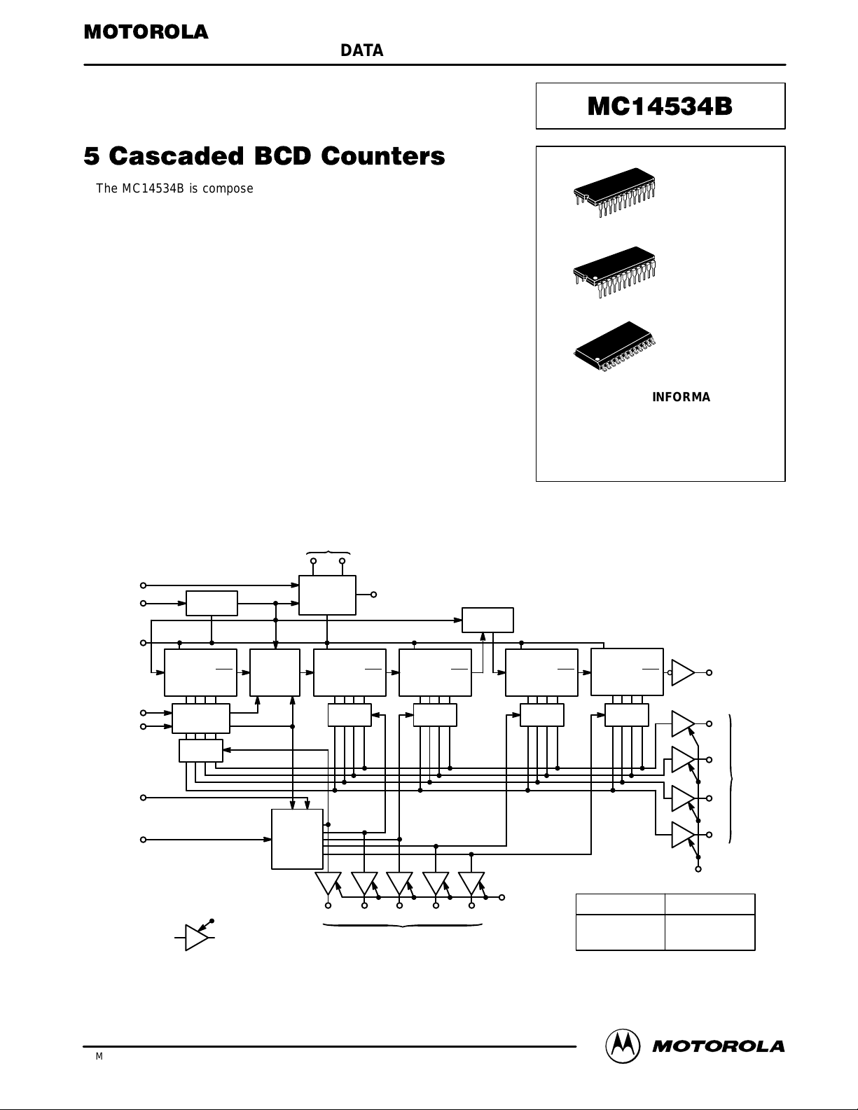
The MC14534B is composed of five BCD ripple counters that have their
respective outputs multiplexed using an internal scanner. Outputs of each
counter are selected by the scanner and appear on four (BCD) p ins.
Selection is indicated by a logic high on the appropriate digit select pin. Both
BCD and digit select outputs have three–state controls providing an
“open–circuit” when these controls are high and allowing multiplexing.
Cascading may be accomplished by using the carry–out pin. The counters
and scanner can be independently reset by applying a high to the counter
master reset (MR) and the scanner r eset (SR). The MC14534B was
specifically designed for application in real time or event counters where
continual updating and multiplexed displays are used.
• Four Operating Modes (See truth table)
• Input Error Detection Circuit
• Clock Conditioning Circuits for Slow Transition Inputs
• Counter Sequences on Positive Transition of Clock A
• Supply Voltage Range = 3.0 Vdc to 18 Vdc
• Capable of Driving Two Low–power TTL Loads or One Low–power
Schottky TTL Load Over the Rated Temperature Range
BLOCK DIAGRAM
PULSE ERROR
DETECTOR
PULSE
SHAPER
TEST
CONTROL
OUTPUT
CONTROL
MUX
MUX MUX MUX MUX
UNITS
CARRY
CONTROL
TENS HUNDREDS THOUSANDS TEN
THOUSANDS
C
÷
10 C ÷ 10 C ÷ 10 C ÷ 10 C ÷ 10
Q0 Q3 Q0 Q3 Q0 Q3 Q0 Q3 Q0 Q3
C
n+4
C
n+4
C
n+4
C
n+4
C
n+4
22
7 8 14 16 11
1
23
4
2
5
6
9
10
CLOCK B
CLOCK A
MASTER
RESET
MODE A
MODE B
SCANNER
RESET
SCANNER
CLOCK
ERROR OUT
3
R
SCANNER
13
17
18
19
20
Q3
Q2
Q1
Q0
21
3–STATE BCD
CONTROL
CARRY OUT
3–STATE DIGIT
CONTROL
15
DS1 DS2 DS3 DS4 DS5
DIGIT SELECT
3–STATE
OUTPUT BUFFER
NOTE:
BCD
OUT
VDD = PIN 24
VSS = PIN 12
TO CAPACITORS
3–State Control Out
Q or DS
High Impedance
0
1
=
SEMICONDUCTOR TECHNICAL DATA
Motorola, Inc. 1995
REV 3
1/94
L SUFFIX
CERAMIC
CASE 623
ORDERING INFORMATION
MC14XXXBCP Plastic
MC14XXXBCL Ceramic
MC14XXXBDW SOIC
TA = – 55° to 125°C for all packages.
P SUFFIX
PLASTIC
CASE 709
DW SUFFIX
SOIC
CASE 751E
MOTOROLA CMOS LOGIC DATAMC14534B
2
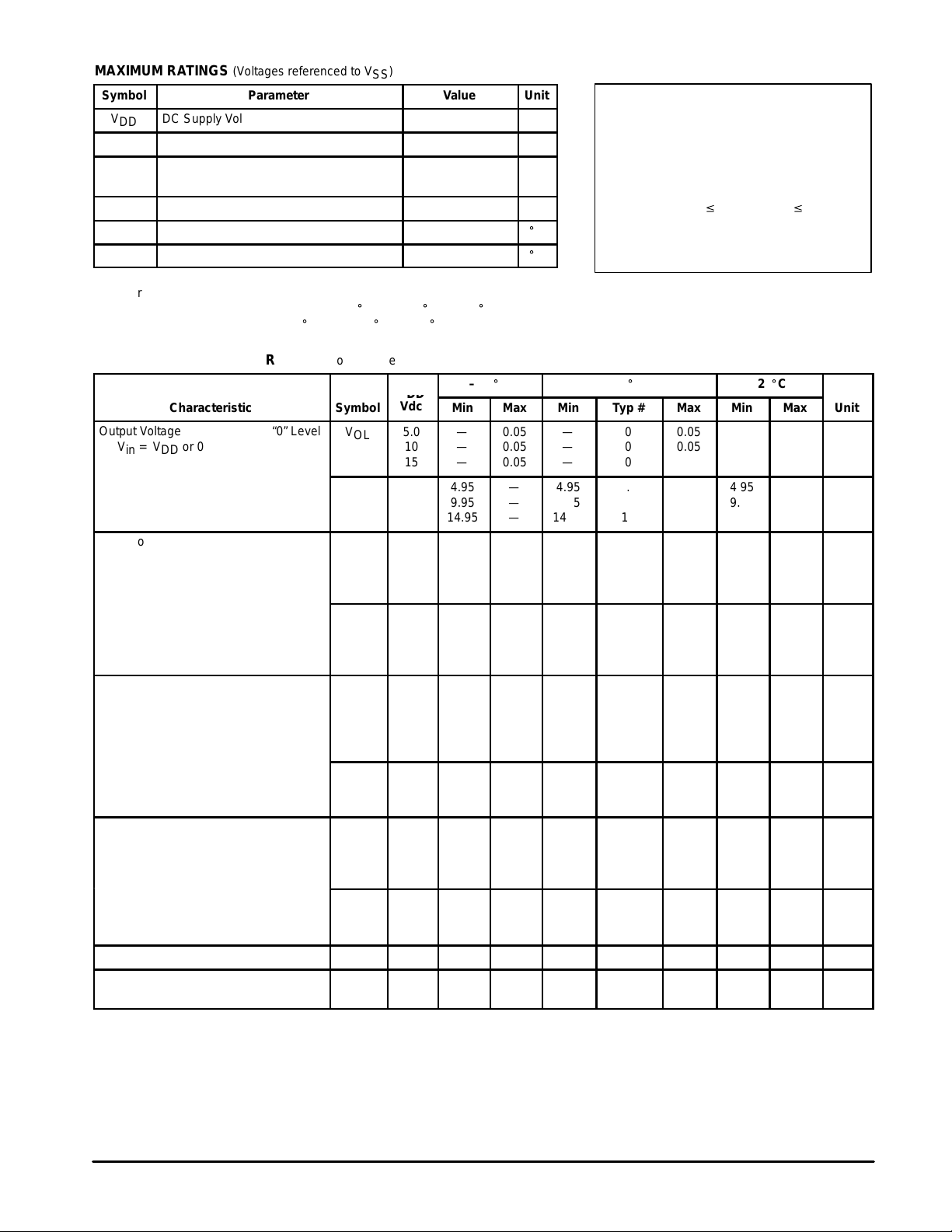
MAXIMUM RATINGS (Voltages referenced to V
SS
)
Symbol
Parameter Value Unit
V
DD
DC Supply Voltage – 0.5 to + 18.0 V
Vin, V
out
Input or Output Voltage (DC or Transient) – 0.5 to VDD + 0.5 V
Iin, I
out
Input or Output Current (DC or Transient),
per Pin
± 10 mA
P
D
Power Dissipation, per Package† 500 mW
T
stg
Storage Temperature – 65 to + 150
_
C
T
L
Lead Temperature (8–Second Soldering) 260
_
C
*Maximum Ratings are those values beyond which damage to the device may occur.
†Temperature Derating:
Plastic “P and D/DW” Packages: – 7.0 mW/_C From 65_C To 125_C
Ceramic “L” Packages: – 12 mW/_C From 100_C To 125_C
ELECTRICAL CHARACTERISTICS (Voltages Referenced to V
SS
)
V
– 55_C 25_C 125_C
Characteristic
Symbol
V
DD
Vdc
Min Max Min Typ # Max Min Max
Unit
V
OL
5.0
10
15
—
—
—
0.05
0.05
0.05
—
—
—
0
0
0
0.05
0.05
0.05
—
—
—
0.05
0.05
0.05
Vdc
V
OH
5.0
10
15
4.95
9.95
14.95
—
—
—
4.95
9.95
14.95
5.0
10
15
—
—
—
4.95
9.95
14.95
—
—
—
Vdc
V
IL
5.0
10
15
—
—
—
1.0
2.0
3.0
—
—
—
1.5
3.0
4.5
1.0
2.0
3.0
—
—
—
1.0
2.0
3.0
Vdc
V
IH
5.0
10
15
4.0
8.0
12
—
—
—
4.0
8.0
12
3.5
7.0
11
—
—
—
4.0
8.0
12
—
—
—
Vdc
I
OH
5.0
5.0
10
15
– 3.0
– 0.64
– 1.6
– 4.2
—
—
—
—
– 2.4
– 0.51
– 1.3
– 3.4
– 4.2
– 0.88
– 2.25
– 8.8
—
—
—
—
– 1.7
– 0.36
– 0.9
– 2.4
—
—
—
—
mAdc
I
OL
5.0
10
15
0.64
1.6
4.2
—
—
—
0.51
1.3
3.4
0.88
2.25
8.8
—
—
—
0.36
0.9
2.4
—
—
—
mAdc
I
OH
5.0
10
15
– 0.31
– 0.31
– 0.9
—
—
– 0.25
– 0.25
– 0.75
– 0.8
– 0.4
– 1.6
—
—
– 0.17
– 0.17
– 0.51
—
—
mAdc
I
OL
5.0
10
15
0.024
0.06
1.3
—
—
—
0.02
0.05
0.25
0.03
0.09
1.63
—
—
—
0.014
0.035
0.175
—
—
—
mAdc
Input Current I
in
15 — ± 0.1 — ± 0.00001 ± 0.1 — ± 1.0 µAdc
Input Capacitance
(Vin = 0)
C
in
— — — — 5.0 7.5 — — pF
#Data labelled “Typ” is not to be used for design purposes but is intended as an indication of the IC’s potential performance. (continued)
This device contains protection circuitry to
guard against damage due to high static
voltages or electric fields. However, precautions must be taken to avoid applications of
any voltage higher than maximum rated voltages to this high–impedance circuit. For proper
operation, Vin and V
out
should be constrained
to the range VSS v (Vin or V
out
) v VDD.
Unused inputs must always be tied to an
appropriate logic voltage level (e.g., either V
SS
or VDD). Unused outputs must be left open.
Output Voltage “0” Level
Vin = VDD or 0
Vin = 0 or V
Input Voltage “0” Level
(VO = 4.5 or 0.5 Vdc)
(VO = 9.0 or 1.0 Vdc)
(VO = 13.5 or 1.5 Vdc)
(VO = 0.5 or 4.5 Vdc)
(VO = 1.0 or 9.0 Vdc)
(VO = 1.5 or 13.5 Vdc)
Output Drive Current
(VOH = 2.5 Vdc) Source
(VOH = 4.6 Vdc)
(VOH = 9.5 Vdc)
(VOH = 13.5 Vdc)
(VOL = 0.4 Vdc) Sink
(VOL = 0.5 Vdc)
(VOL = 1.5 Vdc)
Output Drive Current — Pins 1 and 22
(VOH = 2.5 Vdc)
(VOH = 9.5 Vdc) Source
(VOH = 13.5 Vdc)
(VOL = 0.4 Vdc) Sink
(VOL = 0.5 Vdc)
(VOL = 1.5 Vdc)
DD
“1” Level
“1” Level
MOTOROLA CMOS LOGIC DATA
3
MC14534B
ELECTRICAL CHARACTERISTICS (Voltages Referenced to V
SS
) (continued)
V
– 55_C 25_C 125_C
Characteristic
Symbol
V
DD
Vdc
Min Max Min Typ # Max Min Max
Unit
Quiescent Current
(Per Package)
I
DD
5.0
10
15
—
—
—
5.0
10
20
—
—
—
0.010
0.020
0.030
5.0
10
20
—
—
—
150
300
600
µAdc
Total Supply Current**†
(Dynamic plus Quiescent,
Per Package)
(CL = 50 pF on all outputs, all
buffers switching)
I
T
5.0
10
15
IT = (0.5 µA/kHz) f + I
DD Scan Oscillator
IT = (1.0 µA/kHz) f + I
DD Frequency = 1.0 kHz
IT = (1.5 µA/kHz) f + I
DD
µAdc
Three–State Leakage Current I
TL
15 — ± 0.1 — ± 0.0001 ± 0.1 — ± 3.0 µAdc
#Data labelled “Typ” is not to be used for design purposes but is intended as an indication of the IC’s potential performance.
**The formulas given are for the typical characteristics only at 25_C.
†To calculate total supply current at loads other than 50 pF:
IT(CL) = IT(50 pF) + (CL – 50) Vfk
where: IT is in µA (per package), CL in pF, V = (VDD – VSS) in volts, f in kHz is input frequency, and k = 0.001.
 Loading...