

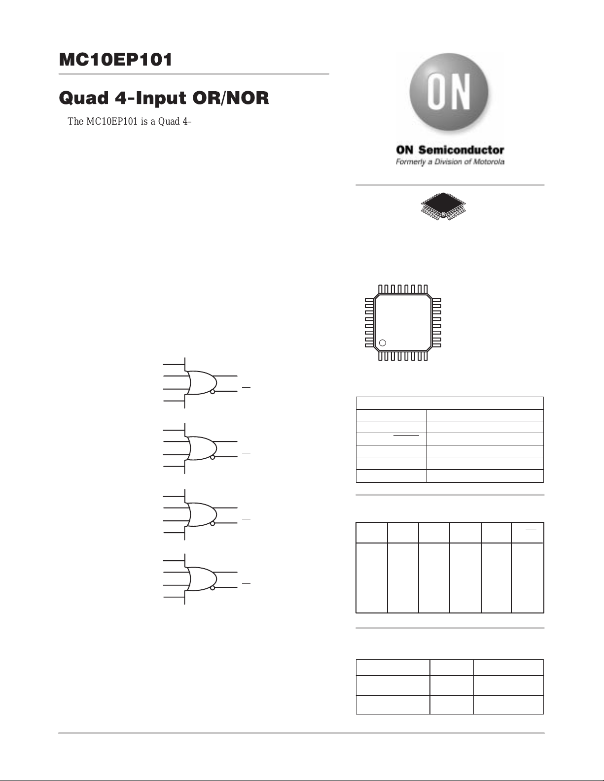
MC10EP101
Quad 4-Input OR/NOR
The MC10EP101 is a Quad 4–input OR/NOR gate. The device is
functionally equivalent to the E101. With AC performance faster than
the E101 device, the EP101 is ideal for applications requiring the
fastest AC performance available. All VCC and VEE pins must be
externally connected to power supply to guarantee proper operation.
• 250ps T ypical Propagation Delay
• High Bandwidth to 3 Ghz T ypical
• PECL mode: 3.0V to 5.5V V
• ECL mode: 0V V
with VEE = –3.0V to –5.5V
CC
• 75kΩ Internal Input Pulldown Resistors
• ESD Protection: >4KV HBM, >100V MM
• Moisture Sensitivity Level 2
For Additional Information, See Application Note AND8003/D
• Flammability Rating: UL–94 code V–0 @ 1/8”,
Oxygen Index 28 to 34
• Transistor Count = 173 devices
LOGIC DIAGRAM
D
0a
D
0b
D
0c
D
0d
D
1a
D
1b
D
1c
D
1d
with VEE = 0V
CC
Q
0
Q
0
Q
1
Q
1
http://onsemi.com
32–LEAD TQFP
FA SUFFIX
CASE 873A
MARKING DIAGRAM*
MC10
EP101
AWLYYWW
32
1
*For additional information, see Application Note
AND8002/D
A = Assembly Location
WL = Wafer Lot
YY = Year
WW = Work Week
PIN DESCRIPTION
PIN
D0a–D3d
Q0–Q3, Q0–Q3
VCC
VBB Reference Voltage Output
VEE Negative, 0 Supply
FUNCTION
ECL Data Inputs
ECL Data Outputs
Positive Supply
D
2a
D
2b
D
2c
D
2d
D
3a
D
3b
D
3c
D
3d
Semiconductor Components Industries, LLC, 1999
March, 2000 – Rev . 1
Q
2
Q
2
Q
3
Q
3
Dna Dnb Dnc Dnd Qn Qn
LLLLLH
HXXXHL
XHXXHL
XXHXHL
XXXHHL
HHHHHL
TRUTH TABLE
ORDERING INFORMATION
Device Package Shipping
MC10EP101FA TQFP 250 Units/Tray
MC10EP101FAR2 TQFP 2000 Tape & Reel
1 Publication Order Number:
MC10EP101/D
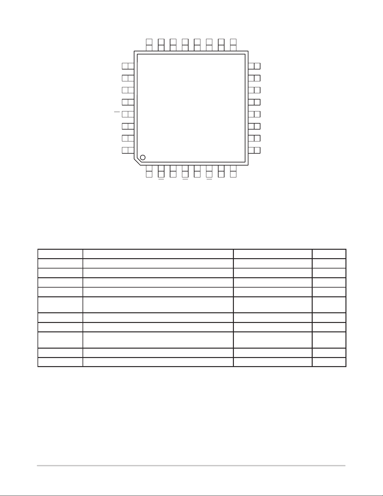
D0c
MC10EP101
24 23 22 21 20 19 18 17
25
D2cD2bD2aD1dD1cD1bD0d D1a
16
D2d
D0b
D0a
VEE
26
27
28
15
14
13
D3a
D3b
VCC
MC10EP101
Q0
Q0
VCC
VCC
29
30
31
32
12345678
Q1
Q2Q2Q1VCC
Figure 1. 32–Lead TQFP Pinout
(Top View)
Warning: All VCC and VEE pins must be externally connected to
Power Supply to guarantee proper operation.
MAXIMUM RATINGS*
Symbol Parameter Value Unit
V
EE
V
CC
V
I
V
I
I
out
T
A
T
stg
θ
JA
θ
JC
T
sol
* Maximum Ratings are those values beyond which damage to the device may occur.
Power Supply (VCC = 0V) –6.0 to 0 VDC
Power Supply (VEE = 0V) 6.0 to 0 VDC
Input Voltage (VCC = 0V, VI not more negative than VEE) –6.0 to 0 VDC
Input Voltage (VEE = 0V, VI not more positive than VCC) 6.0 to 0 VDC
Output Current Continuous
Surge
Operating Temperature Range –40 to +85 °C
Storage Temperature –65 to +150 °C
Thermal Resistance (Junction–to–Ambient) Still Air
500lfpm
Thermal Resistance (Junction–to–Case) 12 to 17 °C/W
Solder Temperature (<2 to 3 Seconds: 245°C desired) 265 °C
12
11
10
9
VCCQ3Q3
D3c
D3d
VEE
NC
50
100
80
55
mA
°C/W
http://onsemi.com
2
MC10EP101
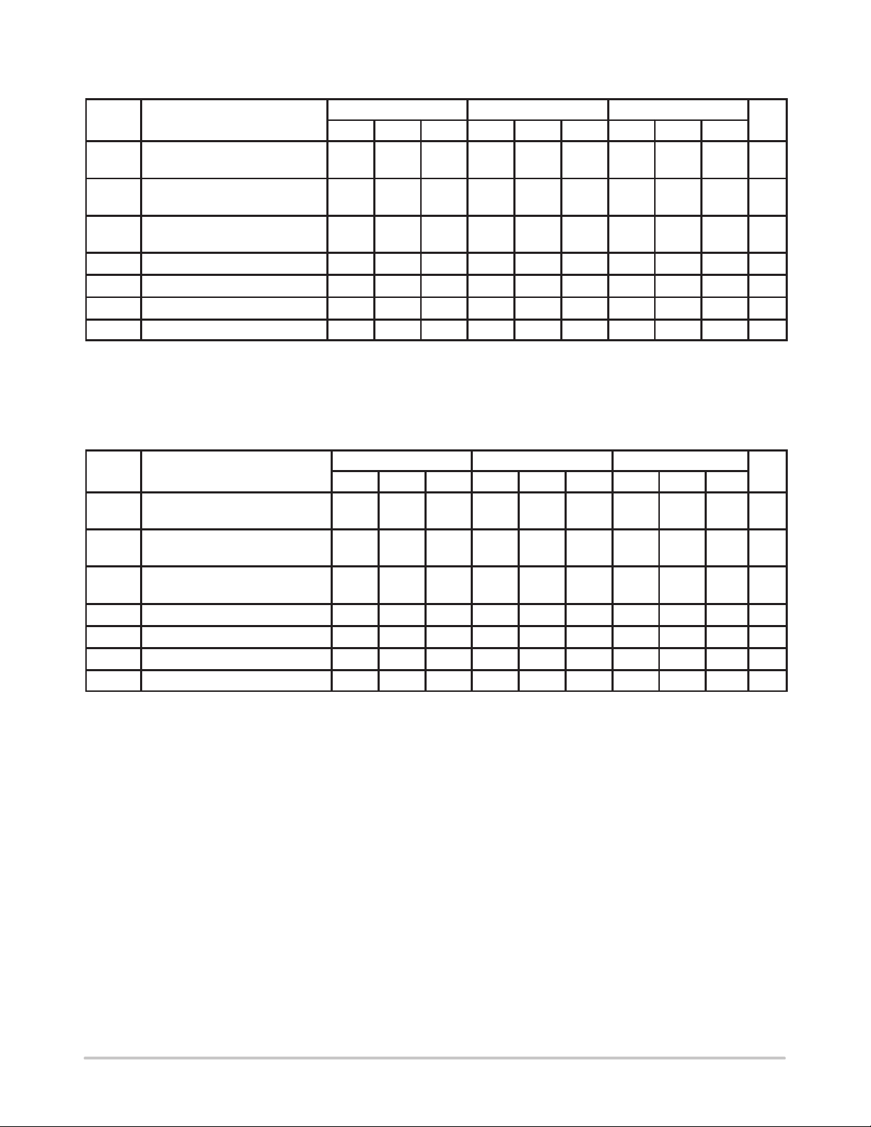
DC CHARACTERISTICS, ECL/LVECL (VCC = 0V, VEE = –5.5V to –3.0V) (Note 3.)
–40°C 25°C 85°C
Symbol Characteristic Min Typ Max Min Typ Max Min Typ Max Unit
IEE
V
OH
V
OL
V
IH
V
IL
I
IH
I
IL
NOTE: 10EP circuits are designed to meet the DC specifications shown in the above table after thermal equilibrium has been established. The
1. VCC = 0V, VEE = V
2. All loading with 50 ohms to VCC –2.0 volts.
3. Input and output parameters vary 1:1 with VCC.
Power Supply Current
(Note 1.)
Output HIGH Voltage
(Note 2.)
Output LOW Voltage
(Note 2.)
Input HIGH Voltage Single Ended –1210 –885 –1145 –820 –1085 –760 mV
Input LOW Voltage Single Ended –1935 –1610 –1870 –1545 –1810 –1485 mV
Input HIGH Current 150 150 150 µA
Input LOW Current –150 –150 –150 µA
circuit is in a test socket or mounted on a printed circuit board and transverse airflow greater than 500lfpm is maintained.
EEmin
to V
, all other pins floating.
EEmax
DC CHARACTERISTICS, LVPECL (VCC = 3.3V ± 0.3V, VEE = 0V) (Note 6.)
Symbol Characteristic Min Typ Max Min Typ Max Min Typ Max Unit
IEE
V
OH
V
OL
V
IH
V
IL
I
IH
I
IL
NOTE: 10EP circuits are designed to meet the DC specifications shown in the above table after thermal equilibrium has been established. The
4. VCC = 3.0V, VEE = 0V, all other pins floating.
5. All loading with 50 ohms to VCC –2.0 volts.
6. Input and output parameters vary 1:1 with VCC.
Power Supply Current
(Note 4.)
Output HIGH Voltage
(Note 5.)
Output LOW Voltage
(Note 5.)
Input HIGH Voltage Single Ended 2090 2415 2155 2480 2215 2540 mV
Input LOW Voltage Single Ended 1365 1690 1430 1755 1490 1815 mV
Input HIGH Current 150 150 150 µA
Input LOW Current –150 –150 –150 µA
circuit is in a test socket or mounted on a printed circuit board and transverse airflow greater than 500lfpm is maintained.
45 57 75 45 58 75 45 59 75 mA
–1135 –1060 –885 –1070 –945 –820 –1010 –885 –760 mV
–1995 –1810 –1685 –1995 –1745 –1620 –1995 –1685 –1560 mV
–40°C 25°C 85°C
45 57 75 45 58 75 45 59 75 mA
2165 2240 2415 2230 2355 2480 2290 2415 2540 mV
1305 1490 1615 1305 1555 1680 1305 1615 1740 mV
http://onsemi.com
3

MC10EP101
DC CHARACTERISTICS, PECL (VCC = 5.0V ± 0.5V, VEE = 0V) (Note 9.)
–40°C 25°C 85°C
Symbol Characteristic Min Typ Max Min Typ Max Min Typ Max Unit
IEE
V
OH
V
OL
V
IH
V
IL
I
IH
I
IL
NOTE: 10EP circuits are designed to meet the DC specifications shown in the above table after thermal equilibrium has been established. The
7. VCC = 5.0V, VEE = 0V, all other pins floating.
8. All loading with 50 ohms to VCC –2.0 volts.
9. Input and output parameters vary 1:1 with VCC.
Power Supply Current
(Note 7.)
Output HIGH Voltage
(Note 8.)
Output LOW Voltage
(Note 8.)
Input HIGH Voltage Single Ended 3790 4115 3855 4180 3915 4240 mV
Input LOW Voltage Single Ended 3065 3390 3130 3455 3190 3515 mV
Input HIGH Current 150 150 150 µA
Input LOW Current –150 –150 –150 µA
circuit is in a test socket or mounted on a printed circuit board and transverse airflow greater than 500lfpm is maintained.
AC CHARACTERISTICS (VCC = 3.0V to 5.5V; VEE = 0V) or (VCC = 0V; VEE = –3.0V to –5.5V)
Symbol Characteristic Min Typ Max Min Typ Max Min Typ Max Unit
f
max
t
PLH
t
PHL
t
SKEW
t
JITTER
t
r
t
f
10.F
11.Skew is measured between outputs under identical transitions.
Maximum Toggle
Frequency (Note 10.)
,
Propagation D –>Q, Q
Delay
Device Skew Q, Q
Part–to–Part (Note 11.)
Cycle–to–Cycle Jitter TBD TBD TBD ps
Output Rise and Fall Times
(20% – 80%) Q, Q
guaranteed for functionality only.
max
45 57 75 45 58 75 45 59 75 mA
3865 3940 4115 3930 4055 4180 3990 4115 4240 mV
3005 3190 3315 3005 3255 3380 3005 3315 3440 mV
–40°C 25°C 85°C
3.0 3.0 3.0 GHz
125 225 325 150 250 370 170 300 420 ps
TBD
TBD
100 150 200 100 170 250 120 190 270 ps
TBD
TBD
TBD
TBD
ps
http://onsemi.com
4

MC10EP101
P ACKAGE DIMENSIONS
TQFP
FA SUFFIX
32–LEAD PLASTIC PACKAGE
CASE 873A–02
ISSUE A
SEATING
PLANE
9
C
–T–
B1
–AB–
–AC–
E
A
A1
32
1
4X
25
T–U0.20 (0.008) ZAB
–T–, –U–, –Z–
–U–
VB
AE
P
DETAIL Y
8
9
–Z–
S1
S
G
0.10 (0.004) AC
_
8X
M
H
W
R
K
X
DETAIL AD
17
4X
_
Q
V1
DETAIL AD
0.250 (0.010)
GAUGE PLANE
T–U0.20 (0.008) Z
AC
BASE
METAL
N
DF
J
SECTION AE–AE
T–U
M
0.20 (0.008) ZAC
AE
DETAIL Y
NOTES:
1. DIMENSIONING AND TOLERANCING PER ANSI
Y14.5M, 1982.
2. CONTROLLING DIMENSION: MILLIMETER.
3. DATUM PLANE –AB– IS LOCATED AT BOTTOM
OF LEAD AND IS COINCIDENT WITH THE LEAD
WHERE THE LEAD EXITS THE PLASTIC BODY AT
THE BOTTOM OF THE PARTING LINE.
4. DATUMS –T–, –U–, AND –Z– TO BE
DETERMINED AT DATUM PLANE –AB–.
5. DIMENSIONS S AND V TO BE DETERMINED AT
SEATING PLANE –AC–.
6. DIMENSIONS A AND B DO NOT INCLUDE
MOLD PROTRUSION. ALLOWABLE PROTRUSION
IS 0.250 (0.010) PER SIDE. DIMENSIONS A AND B
DO INCLUDE MOLD MISMATCH AND ARE
DETERMINED AT DATUM PLANE –AB–.
7. DIMENSION D DOES NOT INCLUDE DAMBAR
PROTRUSION. DAMBAR PROTRUSION SHALL
NOT CAUSE THE D DIMENSION TO EXCEED
0.520 (0.020).
8. MINIMUM SOLDER PLATE THICKNESS SHALL
BE 0.0076 (0.0003).
9. EXACT SHAPE OF EACH CORNER MAY VARY
FROM DEPICTION.
MILLIMETERS
DIMAMIN MAX MIN MAX
7.000 BSC 0.276 BSC
A1 3.500 BSC 0.138 BSC
B 7.000 BSC 0.276 BSC
B1 3.500 BSC 0.138 BSC
C 1.400 1.600 0.055 0.063
D 0.300 0.450 0.012 0.018
E 1.350 1.450 0.053 0.057
F 0.300 0.400 0.012 0.016
G 0.800 BSC 0.031 BSC
H 0.050 0.150 0.002 0.006
J 0.090 0.200 0.004 0.008
K 0.500 0.700 0.020 0.028
__
M 12 REF 12 REF
N 0.090 0.160 0.004 0.006
P 0.400 BSC 0.016 BSC
____
Q 1 5 1 5
R 0.150 0.250 0.006 0.010
S 9.000 BSC 0.354 BSC
S1 4.500 BSC 0.177 BSC
V 9.000 BSC 0.354 BSC
V1 4.500 BSC 0.177 BSC
W 0.200 REF 0.008 REF
X 1.000 REF 0.039 REF
INCHES
http://onsemi.com
5

Notes
MC10EP101
http://onsemi.com
6

Notes
MC10EP101
http://onsemi.com
7

MC10EP101
ON Semiconductor and are trademarks of Semiconductor Components Industries, LLC (SCILLC). SCILLC reserves the right to make changes
without further notice to any products herein. SCILLC makes no warranty , representation or guarantee regarding the suitability of its products for any particular
purpose, nor does SCILLC assume any liability arising out of the application or use of any product or circuit, and specifically disclaims any and all liability ,
including without limitation special, consequential or incidental damages. “Typical” parameters which may be provided in SCILLC data sheets and/or
specifications can and do vary in different applications and actual performance may vary over time. All operating parameters, including “Typicals” must be
validated for each customer application by customer’s technical experts. SCILLC does not convey any license under its patent rights nor the rights of others.
SCILLC products are not designed, intended, or authorized for use as components in systems intended for surgical implant into the body, or other applications
intended to support or sustain life, or for any other application in which the failure of the SCILLC product could create a situation where personal injury or
death may occur. Should Buyer purchase or use SCILLC products for any such unintended or unauthorized application, Buyer shall indemnify and hold
SCILLC and its officers, employees, subsidiaries, affiliates, and distributors harmless against all claims, costs, damages, and expenses, and reasonable
attorney fees arising out of, directly or indirectly , any claim of personal injury or death associated with such unintended or unauthorized use, even if such claim
alleges that SCILLC was negligent regarding the design or manufacture of the part. SCILLC is an Equal Opportunity/Affirmative Action Employer .
PUBLICATION ORDERING INFORMATION
NORTH AMERICA Literature Fulfillment:
Literature Distribution Center for ON Semiconductor
P.O. Box 5163, Denver, Colorado 80217 USA
Phone: 303–675–2175 or 800–344–3860 Toll Free USA/Canada
Fax: 303–675–2176 or 800–344–3867 Toll Free USA/Canada
Email: ONlit@hibbertco.com
Fax Response Line: 303–675–2167 or 800–344–3810 T oll Free USA/Canada
N. American Technical Support: 800–282–9855 Toll Free USA/Canada
EUROPE: LDC for ON Semiconductor – European Support
German Phone: (+1) 303–308–7140 (M–F 1:00pm to 5:00pm Munich Time)
Email: ONlit–german@hibbertco.com
French Phone: (+1) 303–308–7141 (M–F 1:00pm to 5:00pm Toulouse T ime)
Email: ONlit–french@hibbertco.com
English Phone: (+1) 303–308–7142 (M–F 12:00pm to 5:00pm UK Time)
Email: ONlit@hibbertco.com
EUROPEAN TOLL–FREE ACCESS*: 00–800–4422–3781
*Available from Germany, France, Italy, England, Ireland
CENTRAL/SOUTH AMERICA:
Spanish Phone: 303–308–7143 (Mon–Fri 8:00am to 5:00pm MST)
Email: ONlit–spanish@hibbertco.com
ASIA/PACIFIC : LDC for ON Semiconductor – Asia Support
Phone: 303–675–2121 (Tue–Fri 9:00am to 1:00pm, Hong Kong Time)
T oll Free from Hong Kong & Singapore:
001–800–4422–3781
Email: ONlit–asia@hibbertco.com
JAPAN: ON Semiconductor, Japan Customer Focus Center
4–32–1 Nishi–Gotanda, Shinagawa–ku, T okyo, Japan 141–8549
Phone: 81–3–5740–2745
Email: r14525@onsemi.com
ON Semiconductor Website: http://onsemi.com
For additional information, please contact your local
Sales Representative.
http://onsemi.com
8
MC10EP101/D
 Loading...