

MOTOROLA MC10EP101FA, MC10EP101FAR2 Datasheet
MC10EP101
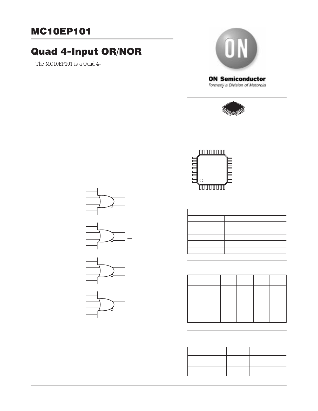
Quad 4-Input OR/NOR
The MC10EP101 is a Quad 4–input OR/NOR gate. The device is
functionally equivalent to the E101. With AC performance faster than
the E101 device, the EP101 is ideal for applications requiring the
fastest AC performance available. All VCC and VEE pins must be
externally connected to power supply to guarantee proper operation.
• 250ps T ypical Propagation Delay
• High Bandwidth to 3 Ghz T ypical
• PECL mode: 3.0V to 5.5V V
• ECL mode: 0V V
with VEE = –3.0V to –5.5V
CC
• 75kΩ Internal Input Pulldown Resistors
• ESD Protection: >4KV HBM, >100V MM
• Moisture Sensitivity Level 2
For Additional Information, See Application Note AND8003/D
• Flammability Rating: UL–94 code V–0 @ 1/8”,
Oxygen Index 28 to 34
• Transistor Count = 173 devices
LOGIC DIAGRAM
D
0a
D
0b
D
0c
D
0d
D
1a
D
1b
D
1c
D
1d
with VEE = 0V
CC
Q
0
Q
0
Q
1
Q
1
http://onsemi.com
32–LEAD TQFP
FA SUFFIX
CASE 873A
MARKING DIAGRAM*
MC10
EP101
AWLYYWW
32
1
*For additional information, see Application Note
AND8002/D
A = Assembly Location
WL = Wafer Lot
YY = Year
WW = Work Week
PIN DESCRIPTION
PIN
D0a–D3d
Q0–Q3, Q0–Q3
VCC
VBB Reference Voltage Output
VEE Negative, 0 Supply
FUNCTION
ECL Data Inputs
ECL Data Outputs
Positive Supply
D
2a
D
2b
D
2c
D
2d
D
3a
D
3b
D
3c
D
3d
Semiconductor Components Industries, LLC, 1999
March, 2000 – Rev . 1
Q
2
Q
2
Q
3
Q
3
Dna Dnb Dnc Dnd Qn Qn
LLLLLH
HXXXHL
XHXXHL
XXHXHL
XXXHHL
HHHHHL
TRUTH TABLE
ORDERING INFORMATION
Device Package Shipping
MC10EP101FA TQFP 250 Units/Tray
MC10EP101FAR2 TQFP 2000 Tape & Reel
1 Publication Order Number:
MC10EP101/D
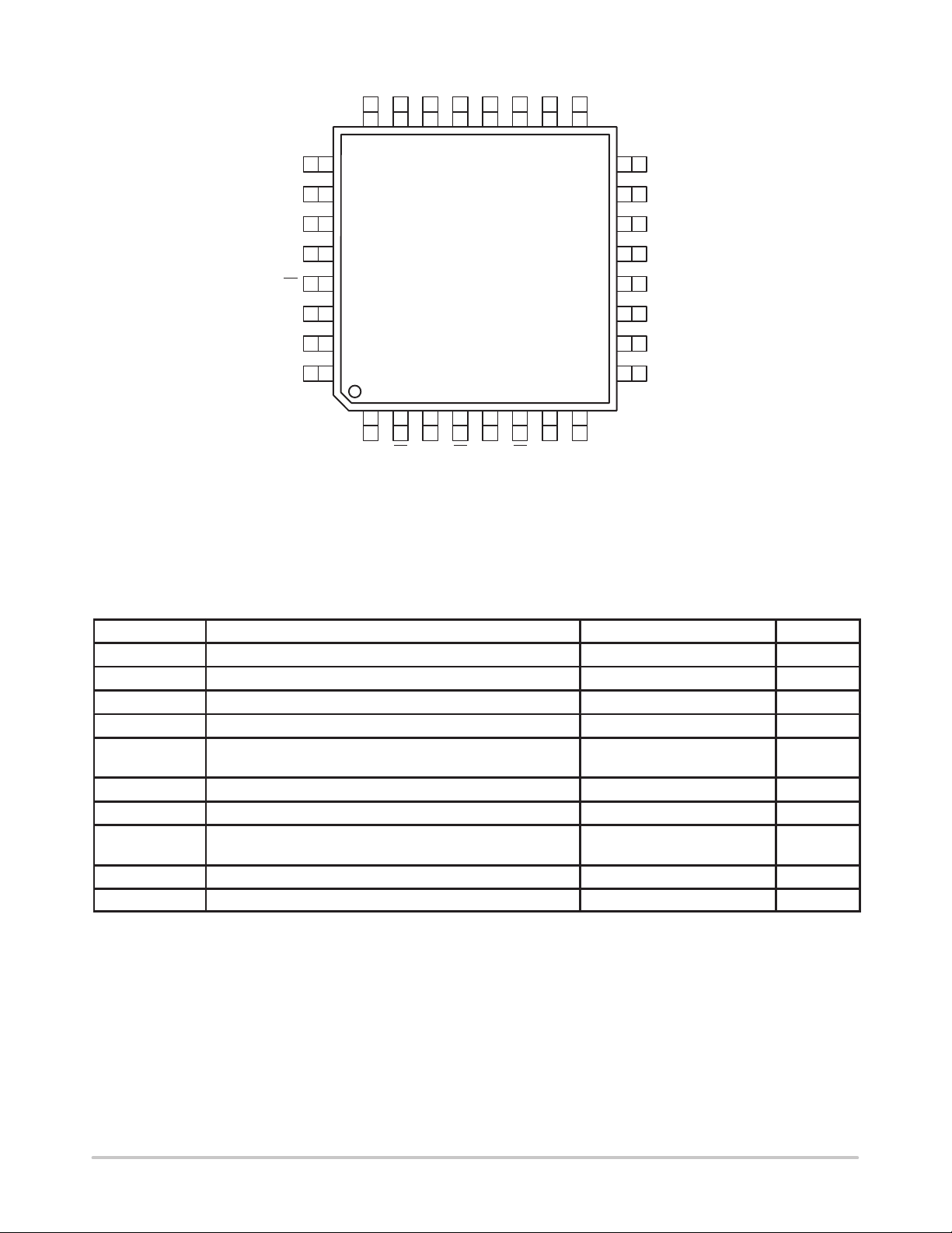
D0c
MC10EP101
24 23 22 21 20 19 18 17
25
D2cD2bD2aD1dD1cD1bD0d D1a
16
D2d
D0b
D0a
VEE
26
27
28
15
14
13
D3a
D3b
VCC
MC10EP101
Q0
Q0
VCC
VCC
29
30
31
32
12345678
Q1
Q2Q2Q1VCC
Figure 1. 32–Lead TQFP Pinout
(Top View)
Warning: All VCC and VEE pins must be externally connected to
Power Supply to guarantee proper operation.
MAXIMUM RATINGS*
Symbol Parameter Value Unit
V
EE
V
CC
V
I
V
I
I
out
T
A
T
stg
θ
JA
θ
JC
T
sol
* Maximum Ratings are those values beyond which damage to the device may occur.
Power Supply (VCC = 0V) –6.0 to 0 VDC
Power Supply (VEE = 0V) 6.0 to 0 VDC
Input Voltage (VCC = 0V, VI not more negative than VEE) –6.0 to 0 VDC
Input Voltage (VEE = 0V, VI not more positive than VCC) 6.0 to 0 VDC
Output Current Continuous
Surge
Operating Temperature Range –40 to +85 °C
Storage Temperature –65 to +150 °C
Thermal Resistance (Junction–to–Ambient) Still Air
500lfpm
Thermal Resistance (Junction–to–Case) 12 to 17 °C/W
Solder Temperature (<2 to 3 Seconds: 245°C desired) 265 °C
12
11
10
9
VCCQ3Q3
D3c
D3d
VEE
NC
50
100
80
55
mA
°C/W
http://onsemi.com
2
MC10EP101
DC CHARACTERISTICS, ECL/LVECL (VCC = 0V, VEE = –5.5V to –3.0V) (Note 3.)
–40°C 25°C 85°C
Symbol Characteristic Min Typ Max Min Typ Max Min Typ Max Unit
IEE
V
OH
V
OL
V
IH
V
IL
I
IH
I
IL
NOTE: 10EP circuits are designed to meet the DC specifications shown in the above table after thermal equilibrium has been established. The
1. VCC = 0V, VEE = V
2. All loading with 50 ohms to VCC –2.0 volts.
3. Input and output parameters vary 1:1 with VCC.
Power Supply Current
(Note 1.)
Output HIGH Voltage
(Note 2.)
Output LOW Voltage
(Note 2.)
Input HIGH Voltage Single Ended –1210 –885 –1145 –820 –1085 –760 mV
Input LOW Voltage Single Ended –1935 –1610 –1870 –1545 –1810 –1485 mV
Input HIGH Current 150 150 150 µA
Input LOW Current –150 –150 –150 µA
circuit is in a test socket or mounted on a printed circuit board and transverse airflow greater than 500lfpm is maintained.
EEmin
to V
, all other pins floating.
EEmax
DC CHARACTERISTICS, LVPECL (VCC = 3.3V ± 0.3V, VEE = 0V) (Note 6.)
Symbol Characteristic Min Typ Max Min Typ Max Min Typ Max Unit
IEE
V
OH
V
OL
V
IH
V
IL
I
IH
I
IL
NOTE: 10EP circuits are designed to meet the DC specifications shown in the above table after thermal equilibrium has been established. The
4. VCC = 3.0V, VEE = 0V, all other pins floating.
5. All loading with 50 ohms to VCC –2.0 volts.
6. Input and output parameters vary 1:1 with VCC.
Power Supply Current
(Note 4.)
Output HIGH Voltage
(Note 5.)
Output LOW Voltage
(Note 5.)
Input HIGH Voltage Single Ended 2090 2415 2155 2480 2215 2540 mV
Input LOW Voltage Single Ended 1365 1690 1430 1755 1490 1815 mV
Input HIGH Current 150 150 150 µA
Input LOW Current –150 –150 –150 µA
circuit is in a test socket or mounted on a printed circuit board and transverse airflow greater than 500lfpm is maintained.
45 57 75 45 58 75 45 59 75 mA
–1135 –1060 –885 –1070 –945 –820 –1010 –885 –760 mV
–1995 –1810 –1685 –1995 –1745 –1620 –1995 –1685 –1560 mV
–40°C 25°C 85°C
45 57 75 45 58 75 45 59 75 mA
2165 2240 2415 2230 2355 2480 2290 2415 2540 mV
1305 1490 1615 1305 1555 1680 1305 1615 1740 mV
http://onsemi.com
3
 Loading...