

MOTOROLA
SEMICONDUCTOR TECHNICAL DATA
3–1
REV 2
Motorola, Inc. 1996
12/93
Coaxial Cable Driver
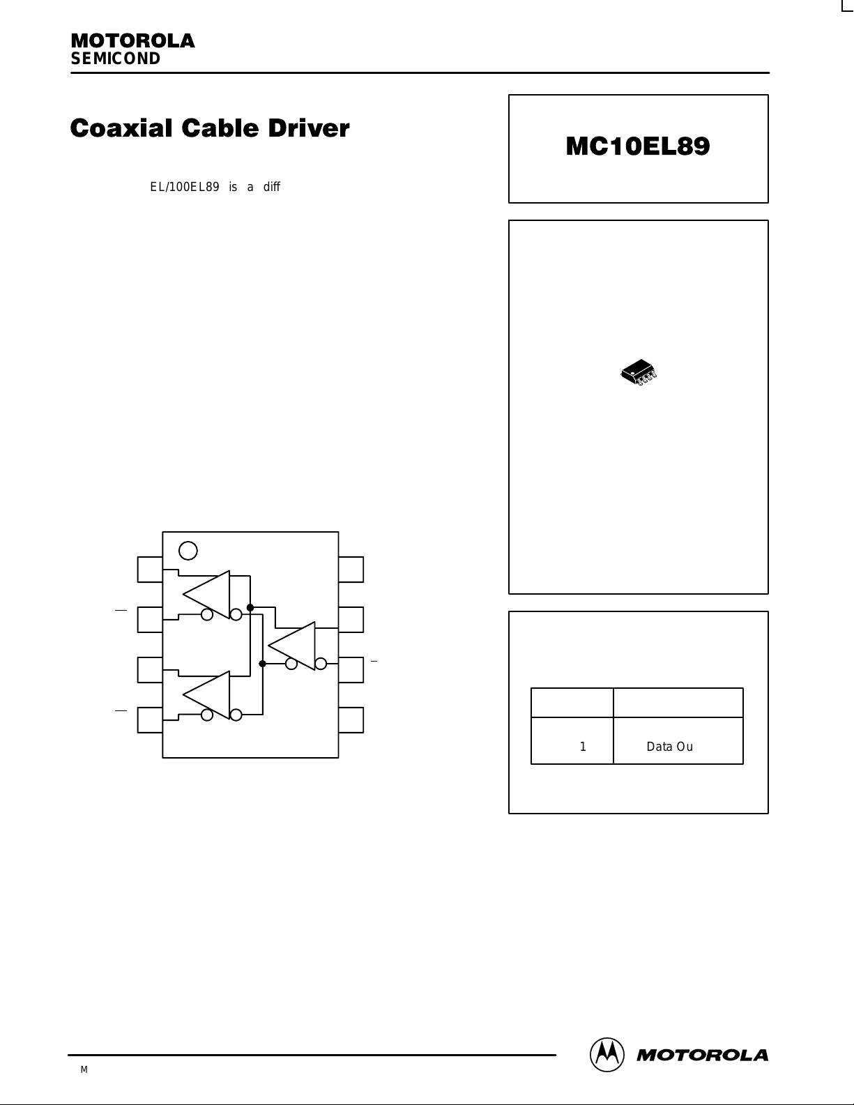
The MC10EL/100EL89 is a differential fanout gate specifically
designed to drive coaxial cables. The device is especially useful in Digital
Video Broadcasting applications; for this application, since the system is
polarity free, each output can be used as an idependent driver. The driver
boasts a gain of approximately 40 and produces output swings twice as
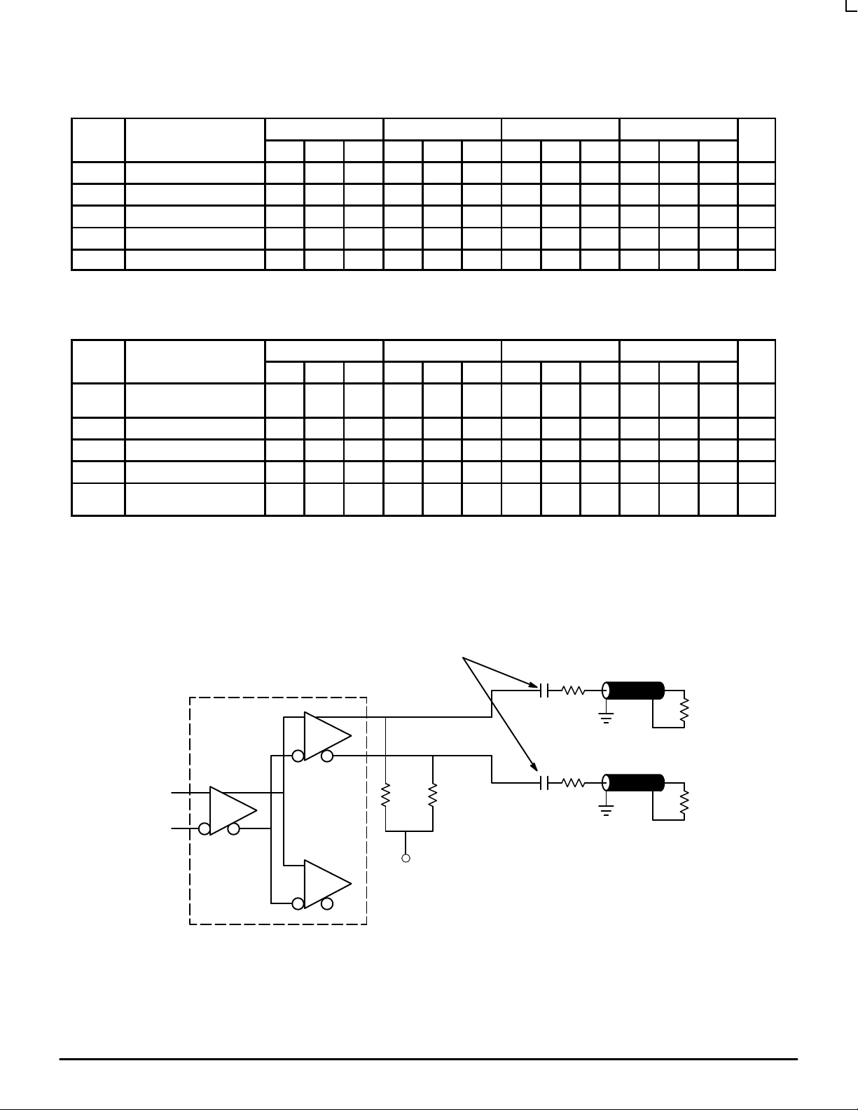
large as a standard ECL output. When driving a coaxial cable, proper
termination is required at both ends of the line to minimize signal loss. The
1.6V output swings allow for termination at both ends of the cable, while
maintaining the required 800mV swing at the receiving end of the cable.
Because of the larger output swings, the device cannot be terminated into
the standard –2.0V. All of the DC parameters are tested with a 50Ω to
–3.0V load. The driver accepts a standard differential ECL input and can
run off of the Digital Video Broadcast standard –5.0V supply.
• 375ps Propagation Delay
• 1.6V Output Swings
• 75kΩ Internal Input Pulldown Resistors
• >1000V ESD Protection
Q0
Q0
Q1
Q1 D
D
5
6
7
8
4
3
2
1
V
EE
V
CC
LOGIC DIAGRAM AND PINOUT ASSIGNMENT
MC10EL89
PIN FUNCTION
D Data Inputs
Q0, Q1 Data Outputs
PIN DESCRIPTION
1
8
D SUFFIX
PLASTIC SOIC PACKAGE
CASE 751-05
MC10EL89
MOTOROLA ECLinPS and ECLinPS Lite
DL140 — Rev 3
3–2
DC CHARACTERISTICS (VEE = VEE(min) to VEE(max); VCC = GND)
–40°C 0°C 25°C 85°C
Symbol Characteristic Min Typ Max Min Typ Max Min Typ Max Min Typ Max Unit
I
EE
Power Supply Current 23 28 23 28 23 28 23 28 mA
V
OH
Output HIGH Voltage
1
–1.23 –1.10 –0.98 –1.17 –1.05 –0.93 –1.13 –1.02 –0.90 –1.06 –0.96 –0.81 V
V
OL
Output LOW Voltage
1
–2.90 –2.72 –2.58 –3.00 –2.70 –2.56 –3.00 –2.70 –2.56 –3.05 –2.67 –2.51 V
V
EE
Power Supply Voltage –4.75 –5.5 –4.75 –5.5 –4.75 –5.5 –4.75 –5.5 V
I
IH
Input HIGH Current 150 150 150 150 µA
1. VOH and VOL specified for 50Ω to –3.0V load.
AC CHARACTERISTICS (VEE = VEE(min) to VEE(max); VCC = GND)
–40°C 0°C 25°C 85°C
Symbol Characteristic Min Typ Max Min Typ Max Min Typ Max Min Typ Max Unit
t
PLH
t
PHL
Propagation Delay to
Output
200 340 480 250 340 430 260 350 440 310 400 490 ps
t
SKEW
Within-Device Skew 5 20 5 20 5 20 5 20
V
PP
Minimum Input Swing
1
150 150 150 150 mV
V
CMR
Common Mode Range
2
–0.4 See2–0.4 See2–0.4 See2–0.4 See2V
t
r
t
f
Output Rise/Fall Times Q
(20% – 80%)
205 330 455 205 330 455 205 330 455 205 330 455 ps
1. Minimum input swing for which AC parameters are guaranteed. The device has a DC gain of ≈40.
2. The CMR range is referenced to the most positive side of the differential input signal. Normal operation is obtained if the HIGH level falls within
the specified range and the peak-to-peak voltage lies between VPPmin and 1V . The lower end of the CMR range is dependent on VEE and is
equal to VEE + 2.5V.
150Ω150
Ω
V
EE
0.1
µ
F
75
Ω
75
Ω
75Ω COAX
0.1µF
75
Ω
75
Ω
75Ω COAX
EL89
DC BLOCKING CAPACITORS
Figure 1. EL89 Termination Configuration
 Loading...