

SEMICONDUCTOR TECHNICAL DATA
3–1
REV 1
Motorola, Inc. 1996
1/95
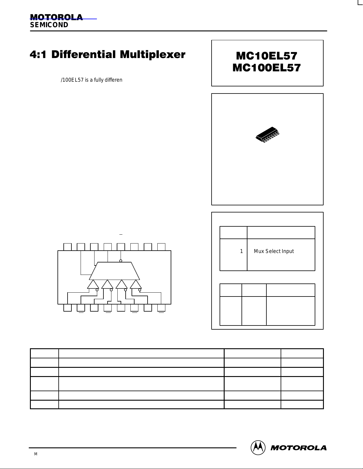
The MC10/100EL57 is a fully differential 4:1 multiplexer . By leaving the
SEL1 line open (pulled LOW via the input pulldown resistors) the device
can also be used as a differential 2:1 multiplexer with SEL0 input
selecting between D0 and D1. The fully differential architecture of the
EL57 makes it ideal for use in low skew applications such as clock
distribution.
The SEL1 is the most significant select line. The binary number applied
to the select inputs will select the same numbered data input (i.e., 00
selects D0).
Multiple VBB outputs are provided for single-ended or AC coupled
interfaces. In these scenarios, the VBB output should be connected to the
data bar inputs and bypassed via a 0.01µF capacitor to ground. Note that
the VBB output can source/sink up to 0.5mA of current without upsetting
the voltage level.
• Useful as Either 4:1 or 2:1 Multiplexer
• V
BB
Output for Single-Ended Operation
• 75kΩ Internal Input Pulldown Resistors
• >1000V ESD Protection
D1
LOGIC DIAGRAM AND PINOUT ASSIGNMENT
D0 D2 D2 D3
1516 14 13 12 11 10
21
3 4 5 6 7
V
CC
9
8
D3
D0
SEL0 SEL1
Q Q V
BB1VBB2VEE
D1
4:1
ABSOLUTE MAXIMUM RATINGS
1
Symbol
Characteristic Rating Unit
V
EE
Power Supply (VCC = 0V) –8.0 to 0 VDC
V
I
Input Voltage (VCC = 0V) 0 to –6.0 VDC
I
out
Output Current Continuous
Surge
50
100
mA
T
A
Operating Temperature Range –40 to +85 °C
V
EE
Operating Range
1,2
–5.7 to –4.2 V
1. Absolute maximum rating, beyond which, device life may be impaired, unless otherwise specified on an individual data sheet.
2. Parametric values specified at: 10EL Series: –4.94V to –5.50V
100EL Series: –4.20V to –5.50V
D0
D1
D2
D3
PIN FUNCTION
D0–3 Diff Data Inputs
SEL0,1 Mux Select Inputs
V
BB
Reference Output
Q0 Data Outputs
PIN DESCRIPTION
SEL1
L
L
H
H
SEL0
L
H
L
H
DATA OUT
FUNCTION TABLE
D SUFFIX
PLASTIC SOIC PACKAGE
CASE 751B-05
1
16
查询MC100E57供应商
MC10EL57 MC100EL57
MOTOROLA ECLinPS and ECLinPS Lite
DL140 — Rev 3
3–2
10EL SERIES
DC CHARACTERISTICS (VEE = VEE(min) – VEE(max); VCC = GND1)
–40°C 0°C 25°C 85°C
Symbol Characteristic Min Max Min Max Min Max Min Max Unit
V
OH
Output HIGH Voltage –1080 –890 –1020 –840 –980 –810 –910 –720 mV
V
OL
Output LOW Voltage –1950 –1650 –1950 –1630 –1950 –1630 –1950 –1595 mV
V
IH
Input HIGH Voltage –1230 –890 –1170 –840 –1130 –810 –1060 –720 mV
V
IL
Input LOW Voltge –1950 –1500 –1950 –1480 –1950 –1480 –1950 –1445 mV
I
IL
Input LOW Current 0.5 — 0.5 — 0.5 — 0.3 — µA
1. 10EL circuits are designed to meet the DC specifications shown in the table after thermal equilibrium has been established. The circuit is in
a test socket or mounted on a printed circuit board and transverse airflow greater than 500lfpm is maintained. Outputs are terminated through
a 50Ω resistor to –2.0V except where otherwise specified on the individual data sheets.
100EL SERIES
DC CHARACTERISTICS (VEE = VEE(min) – VEE(max); VCC = GND1)
–40°C 0°C to 85°C
Symbol Characteristic Min Typ Max Min Typ Max Unit Condition
V
OH
Output HIGH Voltage –1085 –1005 –880 –1025 –955 –880 mV VIN = VIH(max)
V
OL
Output LOW Voltage –1830 –1695 –1555 –1810 –1705 –1620 mV or VIL(min)
V
OHA
Output HIGH Voltage –1095 — — –1035 — — mV VIN = VIH(max)
V
OLA
Output LOW Voltage — — –1555 — — –1610 mV or VIL(min)
V
IH
Input HIGH Voltage –1165 — –880 –1165 — –880 mV
V
IL
Input LOW Voltge –1810 — –1475 –1810 — –1475 mV
I
IL
Input LOW Current 0.5 — — 0.5 — — µA VIN = VIL(max)
1. This table replaces the three tables traditionally seen in ECL 100K data books. The same DC parameter values at VEE = –4.5V now apply across
the full VEE range of –4.2V to –5.5V . Outputs are terminated through a 50Ω resistor to –2.0V except where otherwise specified on the individual
data sheets.
AC/DC CHARACTERISTICS (VEE = VEE(min) to VEE(max); VCC = GND)
–40°C 0°C 25°C 85°C
Symbol Characteristic Min Typ Max Min Typ Max Min Typ Max Min Typ Max Unit
I
EE
Power Supply 10EL
Current 100EL
24
24
24
24
24
24
2427mA
V
BB
Output Reference 10EL
Voltage 100EL
–1.43
–1.38
–1.30
–1.26
–1.38
–1.38
–1.27
–1.26
–1.35
–1.38
–1.25
–1.26
–1.31
–1.38
–1.19
–1.26
V
I
IH
Input High Current 150 150 150 150 µΑ
t
PLH
t
PHL
Propagation DATA→Q/Q
Delay SEL→Q/Q
350
440
550
690
350
440
550
690
360
440
560
690
380
460
580
710
ps
t
SKEW
Input Skew Dn, Dm to Q 100 100 100 100 ps
V
PP
Minimum Input Swing
CLK
250 250 250 250
mV
V
CMR
Common Mode Range
CLK
–2.0 –0.4 –2.0 –0.4 –2.0 –0.4 –2.0 –0.4
V
t
r
t
f
Output Rise/Fall Times Q
(20% – 80%)
125 375 125 375 125 375 125 375 ps

MC10EL57 MC100EL57
3–3 MOTOROLAECLinPS and ECLinPS Lite
DL140 — Rev 3
OUTLINE DIMENSIONS
D SUFFIX
PLASTIC SOIC PACKAGE
CASE 751B-05
ISSUE J
NOTES:
1. DIMENSIONING AND TOLERANCING PER ANSI
Y14.5M, 1982.
2. CONTROLLING DIMENSION: MILLIMETER.
3. DIMENSIONS A AND B DO NOT INCLUDE
MOLD PROTRUSION.
4. MAXIMUM MOLD PROTRUSION 0.15 (0.006)
PER SIDE.
5. DIMENSION D DOES NOT INCLUDE DAMBAR
PROTRUSION. ALLOWABLE DAMBAR
PROTRUSION SHALL BE 0.127 (0.005) TOTAL
IN EXCESS OF THE D DIMENSION AT
MAXIMUM MATERIAL CONDITION.
1 8
16 9
SEATING
PLANE
F
J
M
R
X 45
_
G
8 PLP
–B–
–A–
M
0.25 (0.010) B
S
–T–
D
K
C
16 PL
S
B
M
0.25 (0.010) A
S
T
DIM MIN MAX MIN MAX
INCHESMILLIMETERS
A 9.80 10.00 0.386 0.393
B 3.80 4.00 0.150 0.157
C 1.35 1.75 0.054 0.068
D 0.35 0.49 0.014 0.019
F 0.40 1.25 0.016 0.049
G 1.27 BSC 0.050 BSC
J 0.19 0.25 0.008 0.009
K 0.10 0.25 0.004 0.009
M 0 7 0 7
P 5.80 6.20 0.229 0.244
R 0.25 0.50 0.010 0.019
_ _ _ _
Motorola reserves the right to make changes without further notice to any products herein. Motorola makes no warranty , representation or guarantee regarding
the suitability of its products for any particular purpose, nor does Motorola assume any liability arising out of the application or use of any product or circuit, and
specifically disclaims any and all liability , including without limitation consequential or incidental damages. “Typical” parameters which may be provided in Motorola
data sheets and/or specifications can and do vary in different applications and actual performance may vary over time. All operating parameters, including “Typicals”
must be validated for each customer application by customer’s technical experts. Motorola does not convey any license under its patent rights nor the rights of
others. Motorola products are not designed, intended, or authorized for use as components in systems intended for surgical implant into the body, or other
applications intended to support or sustain life, or for any other application in which the failure of the Motorola product could create a situation where personal injury
or death may occur. Should Buyer purchase or use Motorola products for any such unintended or unauthorized application, Buyer shall indemnify and hold Motorola
and its officers, employees, subsidiaries, affiliates, and distributors harmless against all claims, costs, damages, and expenses, and reasonable attorney fees
arising out of, directly or indirectly, any claim of personal injury or death associated with such unintended or unauthorized use, even if such claim alleges that
Motorola was negligent regarding the design or manufacture of the part. Motorola and are registered trademarks of Motorola, Inc. Motorola, Inc. is an Equal
Opportunity/Affirmative Action Employer.
How to reach us:
USA/EUROPE/Locations Not Listed: Motorola Literature Distribution; JAPAN: Nippon Motorola Ltd.; Tatsumi–SPD–JLDC, 6F Seibu–Butsuryu–Center,
P.O. Box 20912; Phoenix, Arizona 85036. 1–800–441–2447 or 602–303–5454 3–14–2 Tatsumi Koto–Ku, Tokyo 135, Japan. 03–81–3521–8315
MFAX: RMFAX0@email.sps.mot.com – TOUCHTONE 602–244–6609 ASIA/PACIFIC: Motorola Semiconductors H.K. Ltd.; 8B Tai Ping Industrial Park,
INTERNET: http://Design–NET.com 51 Ting Kok Road, Tai Po, N.T., Hong Kong. 852–26629298
MC10EL57/D
*MC10EL57/D*
◊
 Loading...