

MOTOROLA MC100SX1230FN, MC100SX1230FNR2 Datasheet
Order this document
from Logic Marketing
MOTOROLA
SEMICONDUCTOR TECHNICAL DATA
Motorola, Inc. 1994
4/94
REV 0
Advance Information
CMI Coder/Decoder
The MC100SX1230 device consists of a Binary to CMI Coder and CMI
to Binary Decoder with integrated loop back capability. The device is
designed for CMI (Code Mark Inversion) interfaces in transmission
applications supporting either 139.26 Mbit/s E4 or 155.52 Mbit/s STM1
line rates.
• Binary-to-CMI Coder and CMI-to-Binary Decoder
• Internal Loop Back Test Capability
• Supports SDH or PDH Applications
• Low Power
• Fully Differential 100K Compatible I/O
• V
BB
Reference Available
• 75kΩ Input Pulldown Resistors
• +5V PECL or –5V ECL Operation
• 28-Pin Surface Mount PLCC Package
• Asynchronous Reset
In normal operation, the coder and decoder operate independently.
Both the coder and decoder operate from a 2X line rate clock. The device
incorporates test circuitry to support loop back bypass so either the coder
input can be routed to the decoder output or the decoder input can be
routed to the coder output. The part is fabricated using Motorola’s proven
MOSAIC III advanced bipolar process.
The device provides a VBB output for accepting single-ended inputs.
The VBB pin should only be used as a bias for the
MC100SX1230 as its
current sink/source capability is limited. Whenever used, the VBB pin
should be bypassed to ground via a 0.01µF capacitor.
1
DCLK
out
V
CC
V
CC
V
CCO
V
CCO
N/C
N/C
RESET
V
BB
DCLK
in
DCLK
in
V
EE
V
EE
LBIN
LCMI
4
3
2
28
27
26
25
24
23
22
21
20
19
18
17
16
15
14
13
12
11109
7
8
6
5
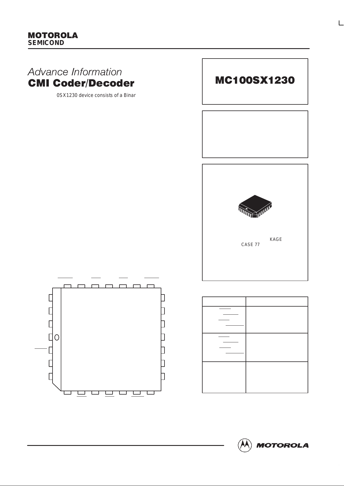
Pinout: 28-Lead PLCC
(Top View)
CMI
in
CCLK
out
CMI
in
QCMI
BIN
in
QCMI
BIN
in
QBIN
CCLK
in
QBIN
CCLK
in
DCLK
out
CCLK
out
MOSAIC III is a trademark of Motorola, Inc.
This document contains information on a new product. Specifications and information herein are subject to
change without notice.
MC100SX1230
CMI CODER/DECODER
FN SUFFIX
PLASTIC PLCC PACKAGE
CASE 776-02
PIN NAMES
Function
CMI Input to Decoder
Decoder Clock Input
Binary Output From Decoder
Decoder Clock Output
Binary Input to Coder
Coder Clock Input
CMI Output from Coder
Coder Clock Output
Asynchronous Reset
Control Input for Binary
Loop Back
Control Input for CMI
Loop Back
Pins
CMIin, CMI
in
DCLKin, DCLK
in
QBIN, QBIN
DCLK
out
, DCLK
out
BINin, BIN
in
CCLKin, CCLK
in
QCMI, QCMI
CCLK
out
, CCLK
out
RESET
LBIN
LCMI
MC100SX1230
2
MOTOROLA High Performance Frequency
Control Products — BR1334
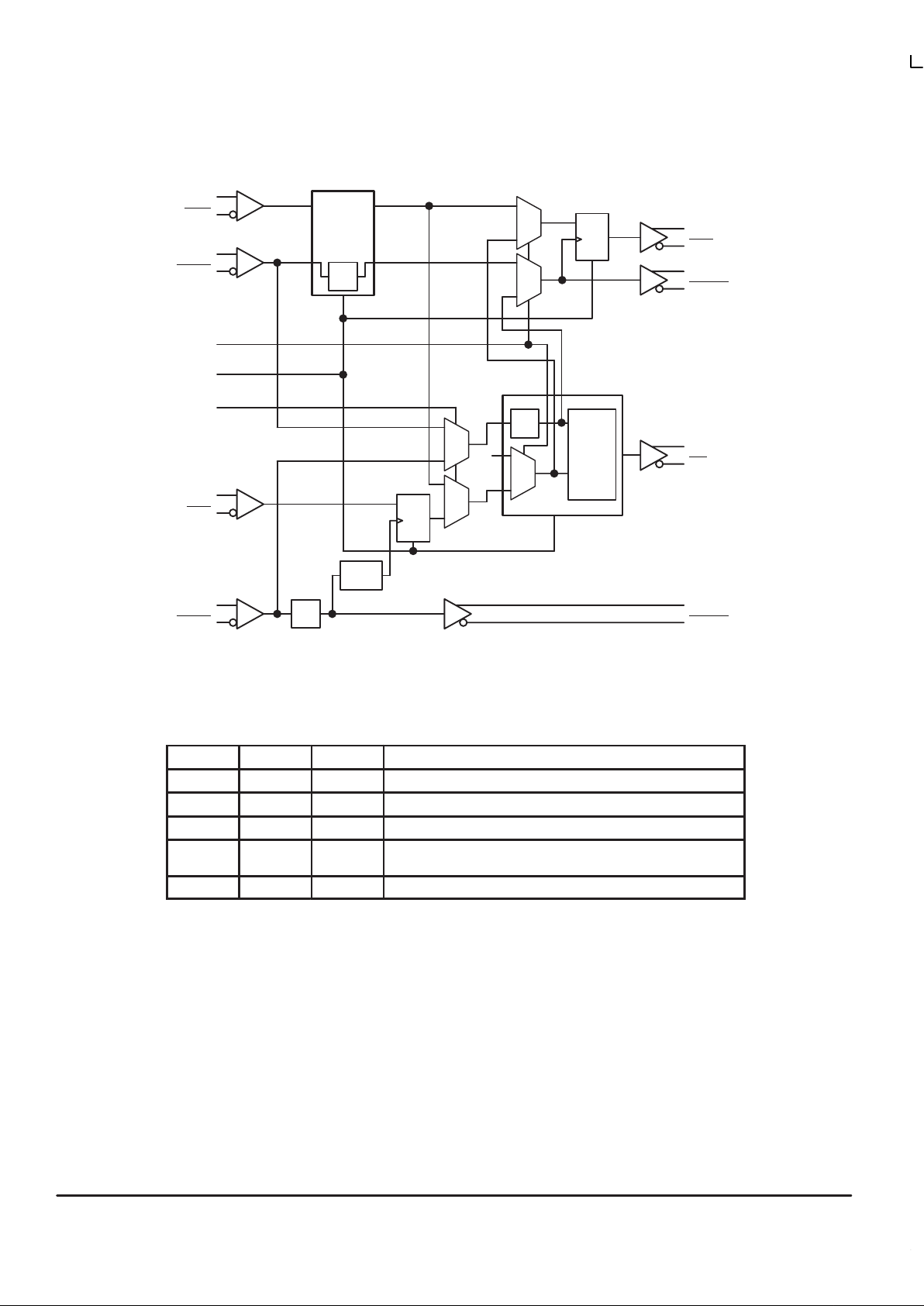
BLOCK DIAGRAM
CMI
in
CMI
in
DCLK
in
DCLK
in
DECODER
÷2
LBIN
QBIN
QBIN
DCLK
out
DCLK
out
D
C
R
CODER
÷2
R
CMI
CMI
H
LCMI
D
C
R
BIN
in
BIN
in
RESET
DELAY
CCLK
in
CCLK
in
÷2
CCLK
out
CCLK
out
FUNCTION TABLE
RESET LBIN LCMI
Function
H X X Reset, All Output Pairs Set to Logic Low State
L L L Independent Coder and Decoder Operation
L L H CMI Input Routed to Coder Output
L H L Binary Input and Clock Routed to Decoder Outputs
Alarm Indication Signal Output from Coder
L H H Illegal, Undefined Operation
MC100SX1230
3
MOTOROLAHigh Performance Frequency
Control Products — BR1334
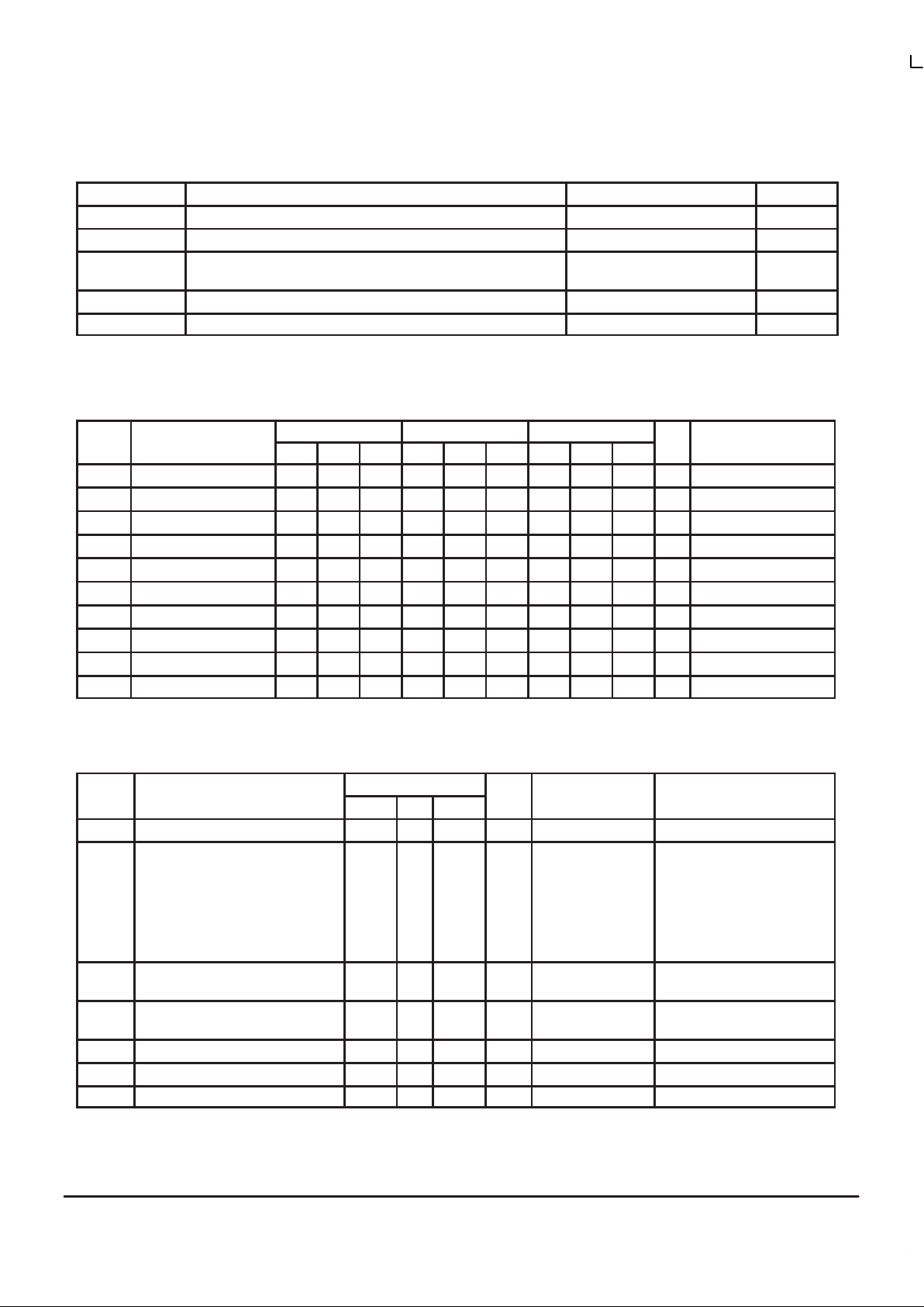
ABSOLUTE MAXIMUM RATINGS
1
Symbol Parameter Value Unit
V
EE
Power Supply (VCC = 0V) –8 to 0 Vdc
V
I
Input Voltage (VCC = 0V) 0 to –6 Vdc
I
OUT
Output Current Continuous
Surge
50
100
mA
T
A
Operating Temperature Range 0 to +85 °C
V
EE
Operating Range
2
–5.7 to 4.2 V
1 Absolute Maximum Ratings are those values beyond which damage to the device may occur. Functional operation should be restricted to the
Recommended Operating Conditions.
2 Parametric values specified at: –4.2 to 5.46V
DC CHARACTERISTICS (VCC = V
CCO
= GND; VEE = –4.2 to 5.46V)
0°C 25°C 85°C
Symbol Characteristic Min Typ Max Min Typ Max Min Typ Max Unit Condition
V
OH
Output HIGH Voltage –1025 –955 –880 –1025 –955 –880 –1025 –955 –880 mV Vin = V
IH(max)
or V
IL(min)
V
OL
Output LOW Voltage –1810 –1705 –1620 –1810 –1705 –1620 –1810 –1705 –1620 mV Vin = V
IH(max)
or V
IL(min)
V
OHA
Output HIGH Voltage –1035 –1035 –1035 mV Vin = V
IH(max)
or V
IL(min)
V
OLA
Output LOW Voltage –1610 –1610 –1610 mV Vin = V
IH(max)
or V
IL(min)
V
IH
Input HIGH Voltage –1165 –880 –1165 –880 –1165 –880 mV
V
IL
Input LOW Voltage –1810 –1475 –1810 –1475 –1810 –1475 mV
V
BB
Reference Voltage –1380 –1260 –1380 –1260 –1380 –1260 V
I
IH
Input HIGH Current 200 200 200 µA
I
IL
Input LOW Current 0.5 0.5 0.5 µA
I
EE
Supply Current 61 122 61 122 70 141 mA
1. 100SX circuits are designed to meet the DC specifications shown in the table after thermal equilibrium has been established. The circuit is mounted in a test socket
or mounted on a printed circuit board and transverse air greater than 500lfm is maintained.
2. All outputs are loaded with 50Ω to VCC – 2V.
AC CHARACTERISTICS (VCC = V
CCO
= GND; VEE = –4.2 to 5.46V)
0 to 85°C
Symbol Characteristic Min Typ Max Unit Condition Notes
F
max
700 MHz
t
pd
Propagation CCLKin to CCLK
out
Delay CCLKin to QCMI
DCLKin to DCLK
out
DCLKin to QBIN
CCLKin to DCLK
out
CCLKin to QBIN
DCLKin to QCMI
650
1000
550
1000
1100
800
1550
1750
1700
1800
2700
1700
ps
LCMI=LBIN=‘L’
LCMI=LBIN=‘L’
LCMI=LBIN=‘L’
LCMI=‘L’, LBIN=‘H’
LCMI=‘L’, LBIN=‘L’
LCMI=‘H’, LBIN=‘L’
Add 3 CCLKin-Cycles to Delay
Add 4 DCLKin-Cycles to Delay
Add 3 CCLKin-Cycles to Delay
Add 5 DCLKin-Cycles to Delay
t
s
Setup Time BINin to CCLK
in
CMIin to DCLK
in
–375
140
ps
t
h
Hold Time CCLKin to BIN
in
DCLKin to CMI
in
1000
120
ps
V
PP
Minimum Input Swing 250 mV
V
CMR
Common Mode Range –0.4 Note V
tr, t
f
Rise/Fall Times 150 700 ps 20% – 80%
1. 100SX circuits are designed to meet the AC specifications shown in the table after thermal equilibrium has been established. The circuit is mounted in a test socket
or mounted on a printed circuit board and transverse air greater than 500lfm is maintained.
2. The CMR range is referenced to the most positive side of the differential input signal. Normal operation is obtained if the HIGH level falls within the specified range
and the peak-to-peak voltage lies between VPPmin and 1V. The lower end of the CMR range is dependent on VEE and is equal to VEE + 3.0V.
 Loading...