Motorola BD810, BD808 Datasheet

1
Motorola Bipolar Power Transistor Device Data
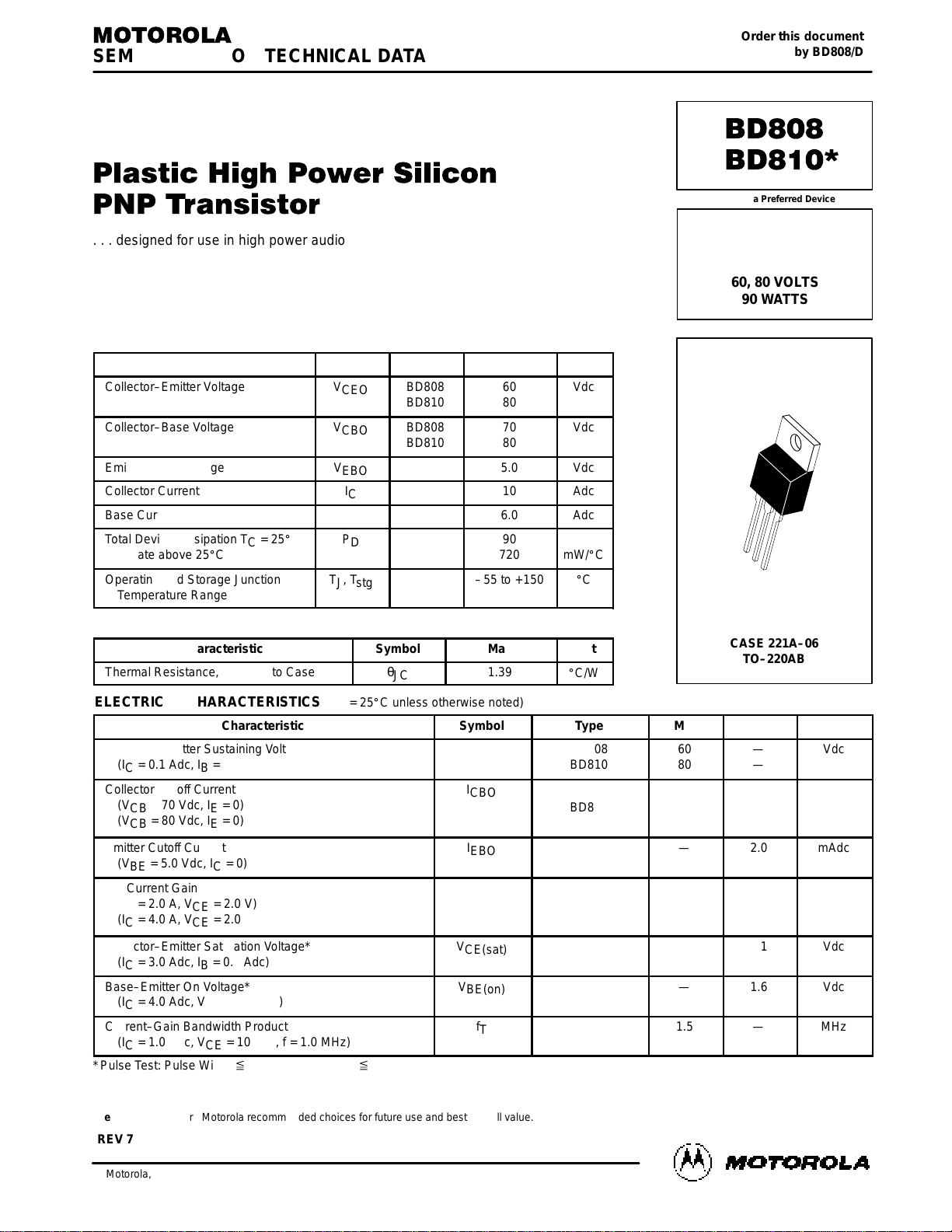
. . . designed for use in high power audio amplifiers utilizing complementary or quasi
complementary circuits.
• DC Current Gain — hFE = 30 (Min) @ IC = 2.0 Adc
• BD 808, 810 are complementary with BD 807, 890
MAXIMUM RATINGS
Rating
Symbol
Type
Value
Unit
Collector–Emitter Voltage
V
CEO
BD808
BD810
60
80
Vdc
Collector–Base Voltage
V
CBO
BD808
BD810
70
80
Vdc
Emitter–Base Voltage
V
EBO
5.0
Vdc
Collector Current
I
C
10
Adc
Base Current
I
B
6.0
Adc
Total Device Dissipation TC = 25_C
Derate above 25_C
P
D
90
720
Watts
mW/_C
Operating and Storage Junction
Temperature Range
TJ, T
stg
–55 to +150
_
C
THERMAL CHARACTERISTICS
Characteristic
Symbol
Max
Unit
Thermal Resistance, Junction to Case
θ
JC
1.39
_
C/W
ELECTRICAL CHARACTERISTICS (T
C
= 25_C unless otherwise noted)
Characteristic
Symbol
Type
Min
Max
Unit
Collector–Emitter Sustaining Voltage*
(IC = 0.1 Adc, IB = 0)
BV
CEO
BD808
BD810
60
80
—
—
Vdc
Collector Cutoff Current
(VCB = 70 Vdc, IE = 0)
(VCB = 80 Vdc, IE = 0)
I
CBO
BD808
BD810
—
—
1.0
1.0
mAdc
Emitter Cutoff Current
(VBE = 5.0 Vdc, IC = 0)
I
EBO
—
2.0
mAdc
DC Current Gain
(IC = 2.0 A, VCE = 2.0 V)
(IC = 4.0 A, VCE = 2.0 V)
h
FE
30
15
—
—
Collector–Emitter Saturation Voltage*
(IC = 3.0 Adc, IB = 0.3 Adc)
V
CE(sat)
—
1.1
Vdc
Base–Emitter On Voltage*
(IC = 4.0 Adc, VCE = 2.0 Vdc)
V
BE(on)
—
1.6
Vdc
Current–Gain Bandwidth Product
(IC = 1.0 Adc, VCE = 10 Vdc, f = 1.0 MHz)
f
T
1.5
—
MHz
*Pulse Test: Pulse Width x 300 µs, Duty Cycle x 2.0%.
Preferred devices are Motorola recommended choices for future use and best overall value.
SEMICONDUCTOR TECHNICAL DATA
Order this document
by BD808/D
Motorola, Inc. 1995
10 AMPERE
POWER TRANSISTORS
PNP SILICON
60, 80 VOLTS
90 WATTS
*Motorola Preferred Device
CASE 221A–06
TO–220AB
REV 7

2
Motorola Bipolar Power Transistor Device Data
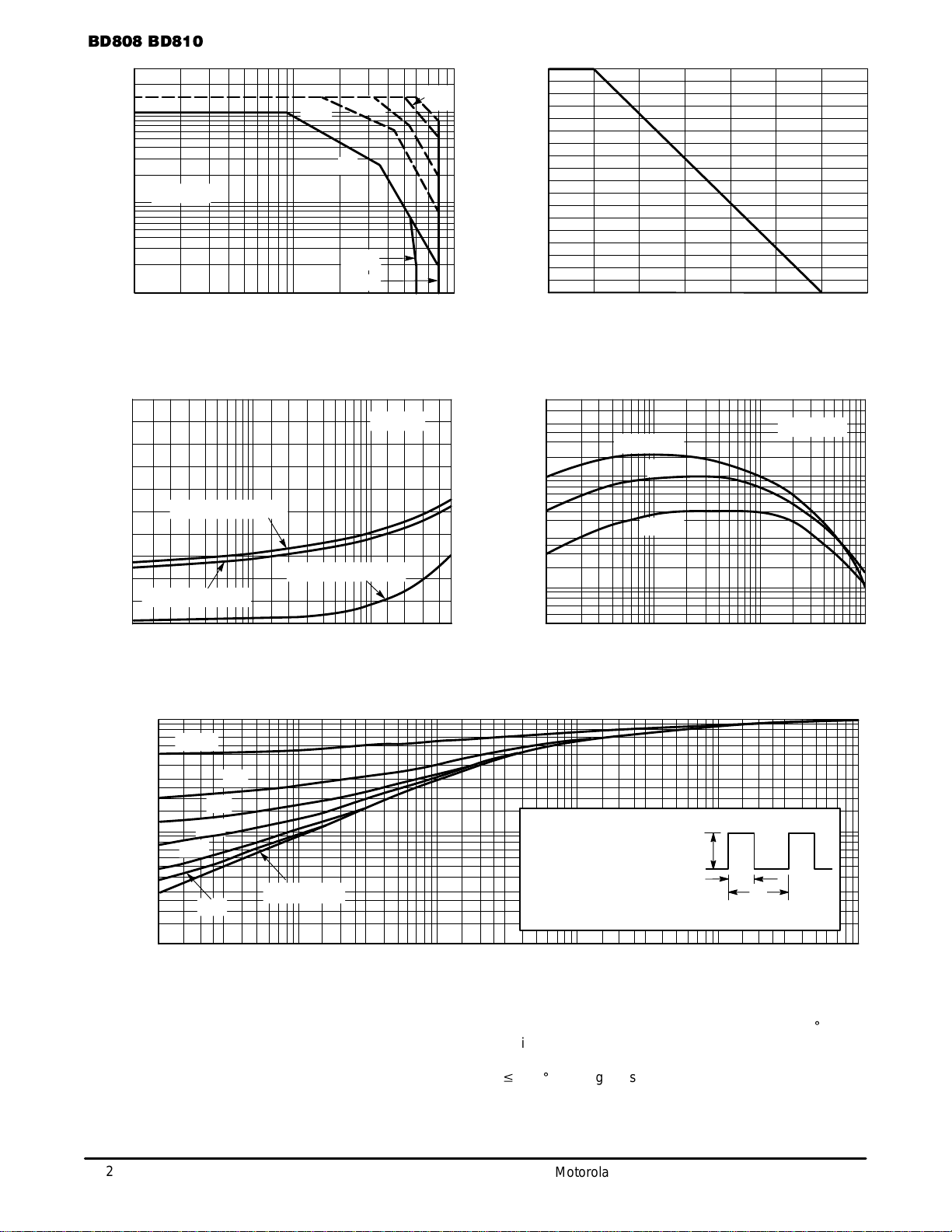
Figure 1. Active Region DC Safe Operating Area
(see Note 1)
10
VCE, COLLECTOR–EMITTER VOLTAGE (VOLTS)
3
1
0.1
3 10 30 100
0.3
I
C
, COLLECTOR CURRENT (AMP)
TJ = 150°C
dc
5 ms
1
1 ms
BD810
BD808
.5 ms
1 ms
90
80
0
0 25 50 100 125 150 175
Figure 2. Power–Temperature Derating Curve
TC, CASE TEMPERATURE (°C)
P
D
, POWER DISSIPATION (WATTS)
75
10
70
60
50
40
30
20
2.0
0.01
IC, COLLECTOR CURRENT (AMP)
1.4
0.8
0.6
0
TJ = 25°C
V
BE(sat)
@ IC/IB = 10
V
CE(sat)
@ IC/IB = 10
VOLTAGE (VOLTS)
Figure 3. “On” Voltages
VBE @ VCE = 2.0 V
Figure 4. Current Gain
IC, COLLECTOR CURRENT (AMPS)
5.0
100
TJ = 150°C
– 55°C
VCE = 2.0 V
h
FE
, DC CURRENT GAIN
500
300
50
10
25°C
0.05 0.10.01 0.5 1.0 105.0
1.8
1.6
1.2
1.0
0.4
0.2
0.02 0.05 0.1 0.2 0.3 0.5 1.0 2.0 3.0 5.0
Figure 5. Thermal Response
t, PULSE WIDTH (ms)
1.0
0.01
0.01
0.7
0.5
0.3
0.2
0.1
0.07
0.05
0.03
0.02
0.02 0.03
r(t), NORMALIZED EFFECTIVE TRANSIENT
THERMAL RESISTANCE
0.05 0.1 0.2 0.3 0.5 1.0 2.0 3.0 5.0 20 30 50 100 200 300 1000500
θ
JC
(t) = r(t)
θ
JC
D CURVES APPLY FOR POWER
PULSE TRAIN SHOWN
READ TIME AT t
1
T
J(pk)
– TC = P
(pk)
θ
JC
(t)
P
(pk)
t
1
t
2
DUTY CYCLE, D = t1/t
2
D = 0.5
SINGLE PULSE
0.2
0.05
0.1
0.02
0.01
SINGLE
PULSE
Note 1:
There are two limitations on the power handling ability of a
transistor: average junction temperature and second breakdown. Safe operating area curves indicate IC – VCE limits of
the transistor that must be observed for reliable operation,
i.e., the transistor must not be subjected to greater dissipation than the curves indicate.
The data of Figure 1 is based on T
J(pk)
= 150_C; TC is
variable depending on conditions. Second breakdown pulse
limits are valid for duty cycles to 1 0% provided T
J(pk)
v
150_C. At high case temperatures, thermal limitations will
reduce the power that can be handled to values less than the
limitations imposed by second breakdown.
 Loading...