


M2V64S40BTP-8A
MITSUBISHI ELECTRIC
PC133 SDRAM (Rev.0.5)
64M bit Synchronous DRAM
FEATURES
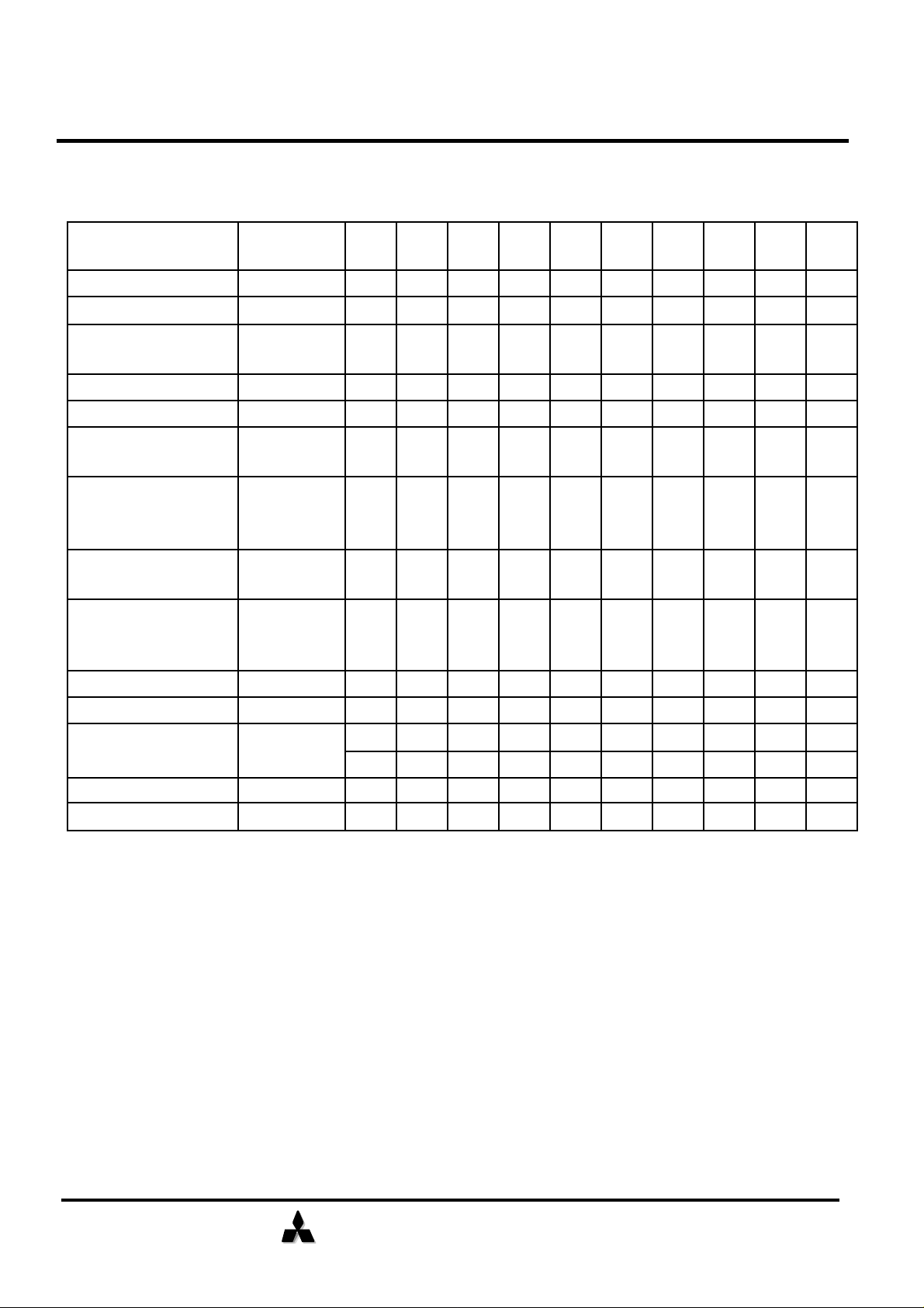
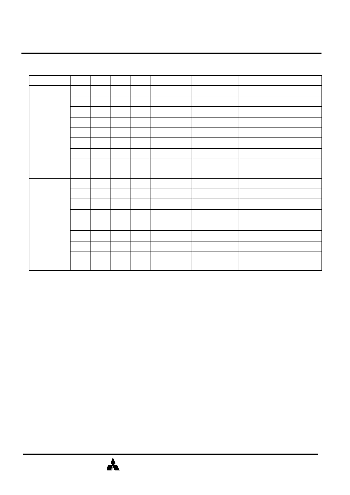
ITEM
M2V64S20TP
Icc1
Icc6
Active to Precharge Command Period
(Min.)
Self Refresh Current
(Max.)
-6
7.5ns45ns
20.0ns
1mA
120mA
M2V64S30TP
M2V64S40TP
Oct. '99
MITSUBISHI LSIs
M2V64S20BTP-6 (4-BANK x 4194304-WORD x 4-BIT)
M2V64S30BTP-6 (4-BANK x 2097152-WORD x 8-BIT)
M2V64S40BTP-6 (4-BANK x 1048576-WORD x 16-BIT)
PRELIMINARY
Some of contents are described for general products and are
subject to change without notice.
DESCRIPTION
M2V64S20BTP is organized as 4-bank x4,194,304-word x 4-bit,and M2V64S30BTP is organized
as 4-bank x 2097152-word x 8-bit ,and M2V64S40BTP is organized as 4-bank x 1048576-word x 16-bit
Synchronous DRAM with LVTTL interface. All inputs and outputs are referenced to the rising edge of
CLK. M2V64S20BTP,M2V64S30BTP,M2V64S40BTP achieves very high speed data rates up to
133MHz, and is suitable for main memory or graphic memory in computer systems.
tCLK
tRAS
tRCD
tAC
tRC
Clock Cycle Time (Min.)
Row to Column Delay (Min.)
Access Time from CLK (Max.) (CL=3)
Ref/Active Command Period (Min.)
Operation Current (Max.) [Single Bank]
5.4ns
67.5ns
- Single 3.3V ±0.3V power supply
- Max. Clock frequency -6 : 133MHz [PC133<3-3-3> ]
- Fully synchronous operation referenced to clock rising edge
- 4-bank operation controlled by BA0,BA1(Bank Address)
- /CAS latency- 2/3 (programmable)
- Burst length- 1/2/4/8/FP (programmable)
- Burst type- Sequential and interleave burst (programmable)
- Random column access
- Auto precharge / All bank precharge controlled by A10
- Auto and self refresh
- 4096 refresh cycles /64ms
- LVTTL Interface
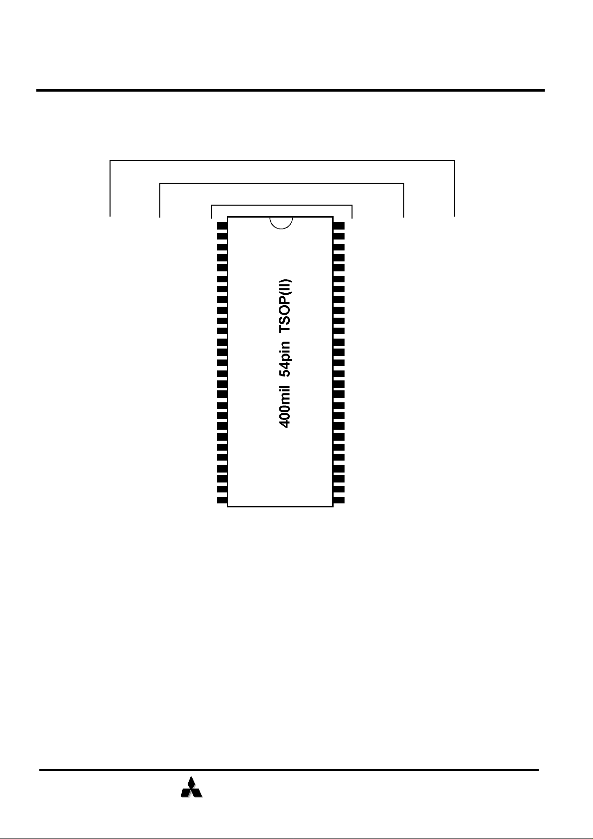
- Package 400-mil, 54-pin Thin Small Outline (TSOP II) with 0.8mm lead pitch
1
MITSUBISHI ELECTRIC
PC133 SDRAM (Rev.0.5)
64M bit Synchronous DRAM
CLK
: Master Clock
CKE
: Clock Enable
/CS
: Chip Select
/RAS
: Row Address Strobe
/CAS
: Column Address Strobe
/WE
: Write Enable
DQ0-3(x4), DQ0-7(x8), DQ0-15(x16)
: Data I/O
DQM (x4, x8) ,DQML/U (x16)
: Output Disable/ Write Mask
A0-11
: Address Input
BA0,1
: Bank Address
Vdd
: Power Supply
VddQ
: Power Supply for Output
Vss
: Ground
VssQ
: Ground for Output
Oct. '99
M2V64S20BTP-6 (4-BANK x 4194304-WORD x 4-BIT)
M2V64S30BTP-6 (4-BANK x 2097152-WORD x 8-BIT)
M2V64S40BTP-6 (4-BANK x 1048576-WORD x 16-BIT)
PIN CONFIGURATION (TOP VIEW)
MITSUBISHI LSIs
M2V64S20BTP
M2V64S30BTP
M2V64S40BTP
Vdd
NC
VddQ
NC
DQ0
VssQ
NC
NC
VddQ
NC
DQ1
VssQ
NC
Vdd
NC
/WE
/CAS
/RAS
/CS
BA0(A13)
BA1(A12)
A10
A0
A1
A2
A3
Vdd
Vdd
DQ0
VddQ
NC
DQ1
VssQ
NC
DQ2
VddQ
NC
DQ3
VssQ
NC
Vdd
NC
/WE
/CAS
/RAS
/CS
BA0(A13)
BA1(A12)
A10
A0
A1
A2
A3
Vdd
Vdd
DQ0
VddQ
DQ1
DQ2
VssQ
DQ3
DQ4
VddQ
DQ5
DQ6
VssQ
DQ7
Vdd
DQML
/WE
/CAS
/RAS
/CS
BA0(A13)
BA1(A12)
A10
Vdd
1
2
3
4
5
6
7
8
9
10
11
12
13
14
15
16
17
18
19
20
21
22
A0
24 31
A1 A6
25 30
A2
26 29
A3
27 28
54
53
52
51
50
49
48
47
46
45
44
43
42
41
40
39
38
37
36
35
34
33
Vss
DQ15
VssQ
DQ14
DQ13
VddQ
DQ12
DQ11
VssQ
DQ10
DQ9
VddQ
DQ8
Vss
NC
DQMU
CLK
CKE
NC
A11
A9
A8
A723 32
A5
A4
Vss
Vss
DQ7
VssQ
NC
DQ6
VddQ
NC
DQ5
VssQ
NC
DQ4
VddQ
NC
Vss
NC
DQM
CLK
CKE
NC
A11
A9
A8
A7
A6
A5
A4
Vss
Vss
NC
VssQ
NC
DQ3
VddQ
NC
NC
VssQ
NC
DQ2
VddQ
NC
Vss
NC
DQM
CLK
CKE
NC
A11
A9
A8
A7
A6
A5
A4
Vss
2
MITSUBISHI ELECTRIC
PC133 SDRAM (Rev.0.5)
64M bit Synchronous DRAM
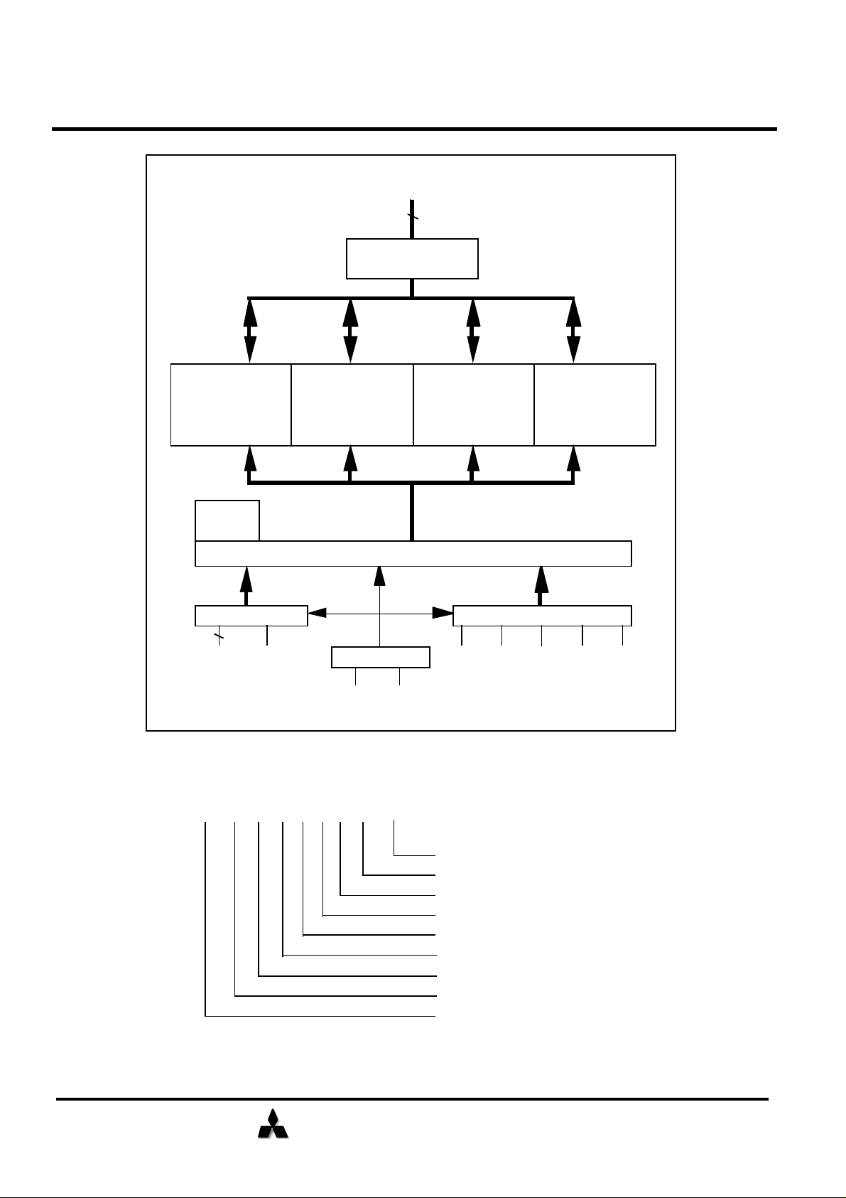
BLOCK DIAGRAM
Address Buffer
Control Signal Buffer
CLK
CKE
Clock Buffer
Control Circuitry
DQ0-15 (x16)
Register
Synchronous DRAM
Oct. '99
MITSUBISHI LSIs
M2V64S20BTP-6 (4-BANK x 4194304-WORD x 4-BIT)
M2V64S30BTP-6 (4-BANK x 2097152-WORD x 8-BIT)
M2V64S40BTP-6 (4-BANK x 1048576-WORD x 16-BIT)
DQ0-3 (x4)
DQ0-7 (x8)
I/O Buffer
Memory Array
Memory Array
Bank #0
Mode
A0-11 BA0,1
Type Designation Code
This rule is applied only to Synchronous DRAM families beyond 64M B-version.
Bank #1
Memory Array
Memory Array
Bank #2
/CS /RAS /CAS /WE DQM
Bank #3
M2 V 64 S 2 0 B TP - 7
Access Item
Package Type TP: TSOP(II)
Process Generation
Function 0: Random Column
Organization 2n 2: x4, 3: x8, 4: x16
Density 64:64M bits
Interface S: SSTL, V:LVTTL
Mitsubishi Semiconductor Memory
3
MITSUBISHI ELECTRIC
PC133 SDRAM (Rev.0.5)
64M bit Synchronous DRAM
PIN FUNCTION
Oct. '99
CLK Input Master Clock: All other inputs are referenced to the rising edge of CLK.
CKE Input
/CS Input Chip Select: When /CS is high, any command means No Operation.
/RAS, /CAS, /WE Input Combination of /RAS, /CAS, /WE defines basic commands.
A0-11 Input
M2V64S20BTP-6 (4-BANK x 4194304-WORD x 4-BIT)
M2V64S30BTP-6 (4-BANK x 2097152-WORD x 8-BIT)
M2V64S40BTP-6 (4-BANK x 1048576-WORD x 16-BIT)
Clock Enable: CKE controls internal clock. When CKE is low, internal clock
for the following cycle is ceased. CKE is also used to select auto / self
refresh. After self refresh mode is started, CKE becomes asynchronous
input. Self refresh is maintained as long as CKE is low.
A0-11 specify the Row / Column Address in conjunction with BA0,1. The
Row Address is specified by A0-11. The Column Address is specified by
A0-A9(x4), A0-A8(x8), A0-7(x16) . A10 is also used to indicate precharge
option. When A10 is high at a read / write command, an auto precharge
is performed. When A10 is high at a precharge command, all banks are
precharged.
MITSUBISHI LSIs
BA0,1 Input
DQ0-3(x4),
DQ0-7(x8),
DQ0-15(x16)
DQM(x4,x8),
DQMU/L(x16)
Vdd, Vss Power Supply Power Supply for the memory array and peripheral circuitry.
VddQ, VssQ Power Supply VddQ and VssQ are supplied to the Output Buffers only.
Input / Output Data In and Data out are referenced to the rising edge of CLK.
Input
Bank Address: BA0,1 specifies one of four banks to which a command is
applied. BA0,1 must be set with ACT, PRE, READ, WRITE commands.
Din Mask / Output Disable: When DQMU/L is high in burst write, Din for the
current cycle is masked. When DQMU/L is high in burst read,
Dout is disabled at the next but one cycle.
4
MITSUBISHI ELECTRIC
PC133 SDRAM (Rev.0.5)
64M bit Synchronous DRAM
BASIC FUNCTIONS
Oct. '99
M2V64S20BTP-6 (4-BANK x 4194304-WORD x 4-BIT)
M2V64S30BTP-6 (4-BANK x 2097152-WORD x 8-BIT)
M2V64S40BTP-6 (4-BANK x 1048576-WORD x 16-BIT)
MITSUBISHI LSIs
The M2V64S20(30,40)BTP provides basic functions, bank (row) activate, burst read / write,
bank (row) precharge, and auto / self refresh.
Each command is defined by control signals of /RAS, /CAS and /WE at CLK rising edge. In
addition to 3 signals, /CS ,CKE and A10 are used as chip select, refresh option, and
precharge option, respectively. To know the detailed definition of commands, please see the
command truth table.
CLK
/CS
/RAS
/CAS
/WE
CKE
A10
Chip Select : L=select, H=deselect
Command
Command
Command
Refresh Option @refresh command
Precharge Option @precharge or read/write command
define basic commands
Activate (ACT) [/RAS =L, /CAS =/WE =H]
ACT command activates a row in an idle bank indicated by BA.
Read (READ) [/RAS =H, /CAS =L, /WE =H]
READ command starts burst read from the active bank indicated by BA. First output data
appears after /CAS latency. When A10 =H at this command, the bank is deactivated after the
burst read (auto-precharge,READA).
Write (WRITE) [/RAS =H, /CAS =/WE =L]
WRITE command starts burst write to the active bank indicated by BA. Total data length to be
written is set by burst length. When A10 =H at this command, the bank is deactivated after the
burst write (auto-precharge, WRITEA).
Precharge (PRE) [/RAS =L, /CAS =H, /WE =L]
PRE command deactivates the active bank indicated by BA. This command also terminates
burst read /write operation. When A10 =H at this command, both banks are deactivated
(precharge all, PREA).
Auto-Refresh (REFA) [/RAS =/CAS =L, /WE =CKE =H]
REFA command starts auto-refresh cycle. Refresh address including bank address are
generated inter-nally. After this command, the banks are precharged automatically.
5
MITSUBISHI ELECTRIC
PC133 SDRAM (Rev.0.5)
64M bit Synchronous DRAM
COMMAND TRUTH TABLE
Oct. '99
MITSUBISHI LSIs
M2V64S20BTP-6 (4-BANK x 4194304-WORD x 4-BIT)
M2V64S30BTP-6 (4-BANK x 2097152-WORD x 8-BIT)
M2V64S40BTP-6 (4-BANK x 1048576-WORD x 16-BIT)
COMMAND MNEMONIC
Deselect DESEL H X H X X X X X X X
No Operation NOP H X L H H H X X X X
Row Address Entry &
Bank Activate
Single Bank Precharge PRE H X L L H L V X L X
Precharge All Banks PREA H X L L H L X H X
Column Address Entry
& Write
Column Address Entry
& Write with Auto-
Precharge
Column Address Entry
& Read
Column Address Entry
& Read with Auto-
Precharge
ACT H X L L H H V V V V
WRITE H X L H L L V X L V
WRITEA H X L H L L V X H V
READ H X L H L H V X L V
READA H X L H L H V X H V
CKE
n-1
CKE
n
/CS /RAS /CAS /WE BA0,1 A11 A10 A0-9
X
Auto-Refresh REFA H H L L L H X X X X
Self-Refresh Entry REFS H L L L L H X X X X
Self-Refresh Exit REFSX
Burst Terminate TBST H X L H H L
Mode Register Set MRS H X L L L L L L L V*1
H=High Level, L=Low Level, V=Valid, X=Don't Care, n=CLK cycle number
NOTE:
1. A7-A9 =0, A0-A6 =Mode Address
L H H X X X X X X X
L H L H H H X X X X
X X X X
6

MITSUBISHI ELECTRIC
PC133 SDRAM (Rev.0.5)
64M bit Synchronous DRAM
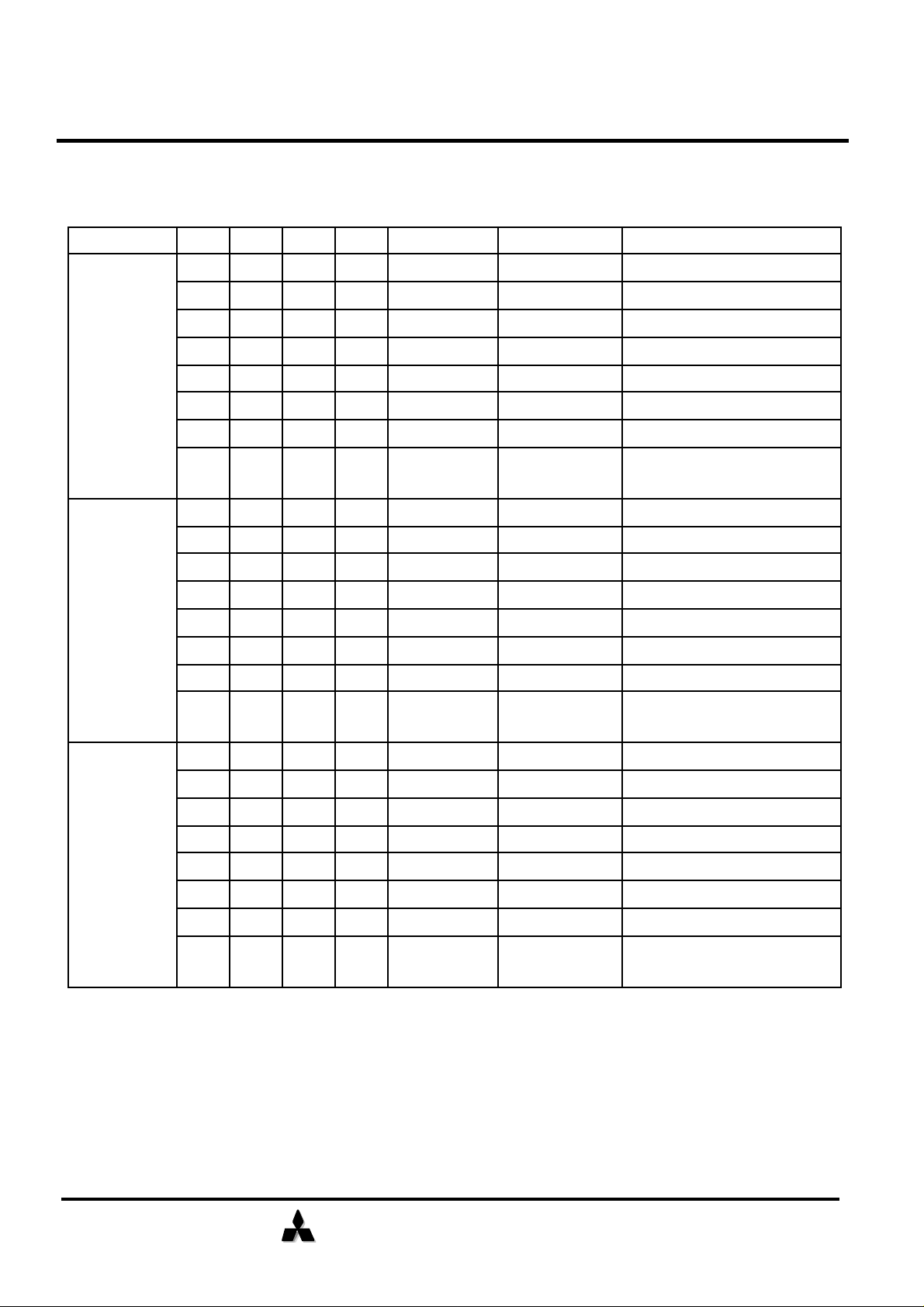
FUNCTION TRUTH TABLE
Oct. '99
Current State /CS /RAS /CAS /WE Address Command Action
IDLE H X X X X DESEL NOP
L H H H X NOP NOP
L H H L BA TBST ILLEGAL*2
L H L X BA, CA, A10 READ / WRITE ILLEGAL*2
L L H H BA, RA ACT Bank Active, Latch RA
L L H L BA, A10 PRE / PREA NOP*4
L L L H X REFA Auto-Refresh*5
M2V64S20BTP-6 (4-BANK x 4194304-WORD x 4-BIT)
M2V64S30BTP-6 (4-BANK x 2097152-WORD x 8-BIT)
M2V64S40BTP-6 (4-BANK x 1048576-WORD x 16-BIT)
MITSUBISHI LSIs
L L L L
ROW ACTIVE H X X X X DESEL NOP
L H H H X NOP NOP
L H H L BA TBST NOP
L H L H BA, CA, A10 READ / READA
L H L L BA, CA, A10
L L H H BA, RA ACT Bank Active / ILLEGAL*2
L L H L BA, A10 PRE / PREA Precharge / Precharge All
L L L H X REFA ILLEGAL
L L L L
READ H X X X X DESEL NOP (Continue Burst to END)
L H H H X NOP NOP (Continue Burst to END)
L H H L BA TBST Terminate Burst
Op-Code,
Mode-Add
Op-Code,
Mode-Add
MRS Mode Register Set*5
Begin Read, Latch CA,
Determine Auto-Precharge
WRITE /
WRITEA
MRS ILLEGAL
Begin Write, Latch CA,
Determine Auto-Precharge
L H L H BA, CA, A10 READ / READA
L H L L BA, CA, A10
L L H H BA, RA ACT Bank Active / ILLEGAL*2
L L H L BA, A10 PRE / PREA Terminate Burst, Precharge
L L L H X REFA ILLEGAL
L L L L
Op-Code,
Mode-Add
Terminate Burst, Latch CA,
Begin New Read, Determine
Auto-Precharge*3
WRITE /
WRITEA
MRS ILLEGAL
Terminate Burst, Latch CA,
Begin Write, Determine AutoPrecharge*3
7
MITSUBISHI ELECTRIC
PC133 SDRAM (Rev.0.5)
64M bit Synchronous DRAM
FUNCTION TRUTH TABLE
(continued)
Oct. '99
Current State /CS /RAS /CAS /WE Address Command Action
WRITE H X X X X DESEL NOP (Continue Burst to END)
L H H H X NOP NOP (Continue Burst to END)
L H H L BA TBST Terminate Burst
L H L H BA, CA, A10 READ / READA
M2V64S20BTP-6 (4-BANK x 4194304-WORD x 4-BIT)
M2V64S30BTP-6 (4-BANK x 2097152-WORD x 8-BIT)
M2V64S40BTP-6 (4-BANK x 1048576-WORD x 16-BIT)
Terminate Burst, Latch CA,
Begin Read, Determine AutoPrecharge*3
MITSUBISHI LSIs
READ with
AUTO
PRECHARGE
L H L L BA, CA, A10
L L H H BA, RA ACT Bank Active / ILLEGAL*2
L L H L BA, A10 PRE / PREA Terminate Burst, Precharge
L L L H X REFA ILLEGAL
L L L L
H X X X X DESEL NOP (Continue Burst to END)
L H H H X NOP NOP (Continue Burst to END)
L H H L BA TBST ILLEGAL
L H L H BA, CA, A10 READ / READA ILLEGAL
L H L L BA, CA, A10
L L H H BA, RA ACT Bank Active / ILLEGAL*2
L L H L BA, A10 PRE / PREA ILLEGAL*2
L L L H X REFA ILLEGAL
L L L L
Op-Code,
Mode-Add
Op-Code,
Mode-Add
WRITE /
WRITEA
MRS ILLEGAL
WRITE /
WRITEA
MRS ILLEGAL
Terminate Burst, Latch CA,
Begin Write, Determine AutoPrecharge*3
ILLEGAL
WRITE with
AUTO
PRECHARGE
H X X X X DESEL NOP (Continue Burst to END)
L H H H X NOP NOP (Continue Burst to END)
L H H L BA TBST ILLEGAL
L H L H BA, CA, A10 READ / READA ILLEGAL
L H L L BA, CA, A10
L L H H BA, RA ACT Bank Active / ILLEGAL*2
L L H L BA, A10 PRE / PREA ILLEGAL*2
L L L H X REFA ILLEGAL
L L L L
Op-Code,
Mode-Add
WRITE /
WRITEA
MRS ILLEGAL
ILLEGAL
8
MITSUBISHI ELECTRIC
PC133 SDRAM (Rev.0.5)
64M bit Synchronous DRAM
FUNCTION TRUTH TABLE
(continued)
Oct. '99
Current State /CS /RAS /CAS /WE Address Command Action
M2V64S20BTP-6 (4-BANK x 4194304-WORD x 4-BIT)
M2V64S30BTP-6 (4-BANK x 2097152-WORD x 8-BIT)
M2V64S40BTP-6 (4-BANK x 1048576-WORD x 16-BIT)
MITSUBISHI LSIs
PRE -
CHARGING
ROW
ACTIVATING
H X X X X DESEL NOP (Idle after tRP)
L H H H X NOP NOP (Idle after tRP)
L H H L BA TBST ILLEGAL*2
L H L X BA, CA, A10 READ / WRITE ILLEGAL*2
L L H H BA, RA ACT ILLEGAL*2
L L H L BA, A10 PRE / PREA NOP*4 (Idle after tRP)
L L L H X REFA ILLEGAL
L L L L
H X X X X DESEL NOP (Row Active after tRCD)
L H H H X NOP NOP (Row Active after tRCD)
L H H L BA TBST ILLEGAL*2
L H L X BA, CA, A10 READ / WRITE ILLEGAL*2
L L H H BA, RA ACT ILLEGAL*2
L L H L BA, A10 PRE / PREA ILLEGAL*2
L L L H X REFA ILLEGAL
L L L L
Op-Code,
Mode-Add
Op-Code,
Mode-Add
MRS ILLEGAL
MRS ILLEGAL
WRITE RECOVERING
H X X X X DESEL NOP
L H H H X NOP NOP
L H H L BA TBST ILLEGAL*2
L H L X BA, CA, A10 READ / WRITE ILLEGAL*2
L L H H BA, RA ACT ILLEGAL*2
L L H L BA, A10 PRE / PREA ILLEGAL*2
L L L H X REFA ILLEGAL
L L L L
Op-Code,
Mode-Add
MRS ILLEGAL
9
MITSUBISHI ELECTRIC
PC133 SDRAM (Rev.0.5)
64M bit Synchronous DRAM
FUNCTION TRUTH TABLE
(continued)
Oct. '99
Current State /CS /RAS /CAS /WE Address Command Action
M2V64S20BTP-6 (4-BANK x 4194304-WORD x 4-BIT)
M2V64S30BTP-6 (4-BANK x 2097152-WORD x 8-BIT)
M2V64S40BTP-6 (4-BANK x 1048576-WORD x 16-BIT)
MITSUBISHI LSIs
RE-
FRESHING
MODE
REGISTER
SETTING
H X X X X DESEL NOP (Idle after tRC)
L H H H X NOP NOP (Idle after tRC)
L H H L BA TBST ILLEGAL
L H L X BA, CA, A10 READ / WRITE ILLEGAL
L L H H BA, RA ACT ILLEGAL
L L H L BA, A10 PRE / PREA ILLEGAL
L L L H X REFA ILLEGAL
L L L L
H X X X X DESEL NOP (Idle after tRSC)
L H H H X NOP NOP (Idle after tRSC)
L H H L BA TBST ILLEGAL
L H L X BA, CA, A10 READ / WRITE ILLEGAL
L L H H BA, RA ACT ILLEGAL
L L H L BA, A10 PRE / PREA ILLEGAL
L L L H X REFA ILLEGAL
L L L L
Op-Code,
Mode-Add
Op-Code,
Mode-Add
MRS ILLEGAL
MRS ILLEGAL
ABBREVIATIONS:
H=High Level, L=Low Level, X=Don't Care
BA=Bank Address, RA=Row Address, CA=Column Address, NOP=No OPeration
NOTES:
1. All entries assume that CKE was High during the preceding clock cycle and the current clock cycle.
2. ILLEGAL to bank in specified state; function may be legal in the bank indicated by BA, depending on the
state of that bank.
3. Must satisfy bus contention, bus turn around, write recovery requirements.
4. NOP to bank precharging or in idle state. May precharge bank indicated by BA.
5. ILLEGAL if any bank is not idle.
ILLEGAL = Device operation and/or data-integrity are not guaranteed.
10
MITSUBISHI ELECTRIC
PC133 SDRAM (Rev.0.5)
64M bit Synchronous DRAM
FUNCTION TRUTH TABLE for CKE
Oct. '99
MITSUBISHI LSIs
M2V64S20BTP-6 (4-BANK x 4194304-WORD x 4-BIT)
M2V64S30BTP-6 (4-BANK x 2097152-WORD x 8-BIT)
M2V64S40BTP-6 (4-BANK x 1048576-WORD x 16-BIT)
Current State
SELF-
REFRESH*1
POWER
DOWN
ALL BANKS
IDLE*2
CKE
CKE
n-1
H X X X X X X INVALID
L H H X X X X Exit Self-Refresh (Idle after tRC)
L H L H H H X Exit Self-Refresh (Idle after tRC)
L H L H H L X ILLEGAL
L H L H L X X ILLEGAL
L H L L X X X ILLEGAL
L L X X X X X NOP (Maintain Self-Refresh)
H X X X X X X INVALID
L H X X X X X Exit Power Down to Idle
L L X X X X X NOP (Maintain Self-Refresh)
H H X X X X X Refer to Function Truth Table
H L L L L H X Enter Self-Refresh
H L H X X X X Enter Power Down
H L L H H H X Enter Power Down
H L L H H L X ILLEGAL
/CS /RAS /CAS /WE Add Action
n
H L L H L X X ILLEGAL
H L L L X X X ILLEGAL
L X X X X X X Refer to Current State =Power Down
ANY STATE
other than
listed above
ABBREVIATIONS:
H=High Level, L=Low Level, X=Don't Care
NOTES:
1. CKE Low to High transition will re-enable CLK and other inputs asynchronously. A minimum setup
time must be satisfied before any command other than EXIT.
2. Power-Down and Self-Refresh can be entered only from the All Banks Idle State.
3. Must be legal command.
H H X X X X X Refer to Function Truth Table
H L X X X X X Begin CLK Suspend at Next Cycle*3
L H X X X X X Exit CLK Suspend at Next Cycle*3
L L X X X X X Maintain CLK Suspend
11

MITSUBISHI ELECTRIC
PC133 SDRAM (Rev.0.5)
64M bit Synchronous DRAM
SIMPLIFIED STATE DIAGRAM
Oct. '99
MITSUBISHI LSIs
M2V64S20BTP-6 (4-BANK x 4194304-WORD x 4-BIT)
M2V64S30BTP-6 (4-BANK x 2097152-WORD x 8-BIT)
M2V64S40BTP-6 (4-BANK x 1048576-WORD x 16-BIT)
SELF
REFRESH
REFS
REFSX
WRITE
SUSPEND
MODE
REGISTER
SET
CLK
SUSPEND
CKEH
TBST (for Full Page)
WRITE READ
CKEL
WRITE
CKEH
MRS
IDLE
CKEL
ROW
ACTIVE
WRITEA
WRITE
ACT
READA
READ
REFA
CKEL
CKEH
TBST (for Full Page)
READ
AUTO
REFRESH
POWER
DOWN
CKEL
CKEH
READ
SUSPEND
WRITEA
WRITEA
SUSPEND
POWER
APPLIED
CKEL
CKEH
POWER
ON
WRITEA
PRE
WRITEA
PRE
PRE PRE
PRE
CHARGE
12
READA
READA
READA
CKEL
CKEH
READA
SUSPEND
Automatic Sequence
Command Sequence
MITSUBISHI ELECTRIC
PC133 SDRAM (Rev.0.5)
64M bit Synchronous DRAM
POWER ON SEQUENCE
MODE REGISTER
Oct. '99
M2V64S20BTP-6 (4-BANK x 4194304-WORD x 4-BIT)
M2V64S30BTP-6 (4-BANK x 2097152-WORD x 8-BIT)
M2V64S40BTP-6 (4-BANK x 1048576-WORD x 16-BIT)
MITSUBISHI LSIs
Before starting normal operation, the following power on sequence is necessary to prevent a
SDRAM from damaged or malfunctioning.
1.Clock will be applied at power up along with power. Attempt to maintain CKE high,
DQM (x4,x8), DQMU/L (x16) high and NOP condition at the inputs along with power.
2. Maintain stable power, stable clock, and NOP input conditions for a minimum of 200us.
3. Issue precharge commands for all banks. (PRE or PREA)
4. After all banks become idle state (after tRP), issue 8 or more auto-refresh commands.
5. Issue a mode register set command to initialize the mode register.
After these sequence, the SDRAM is idle state and ready for normal operation.
Burst Length, Burst Type and /CAS Latency can be
programmed by setting the mode register (MRS). The mode
register stores these data until the next MRS command, which
may be issued when both banks are in idle state. After tRSC
from a MRS command, the SDRAM is ready for new command.
A11 A10 A9 A8 A7 A6 A5 A4 A3 A2 A1 A0BA1BA0
WM
0 0
/CAS LATENCY
R
R
2
3
R
R
R
R
LTMODE BT BL
BURST
LENGTH
LATENCY
MODE
00
CL
0 0 0
0 0 1
0 1 0
0 1 1
1 0 0
1 0 1
1 1 0
1 1 1
0 0
CLK
/CS
/RAS
/CAS
/WE
BA0,1 A11-A0
BL
0 0 0
0 0 1
0 1 0
0 1 1
1 0 0
1 0 1
1 1 0
1 1 1
BT= 0 BT= 1
1
2
4
8
R
R
R
FP
V
1
2
4
8
R
R
R
R
WRITE
MODE
0
1
BURST
SINGLE BIT
13
BURST
TYPE
0
SEQUENTIAL
1
R: Reserved for Future Use
FP: Full Page
INTERLEAVE
MITSUBISHI ELECTRIC
PC133 SDRAM (Rev.0.5)
64M bit Synchronous DRAM
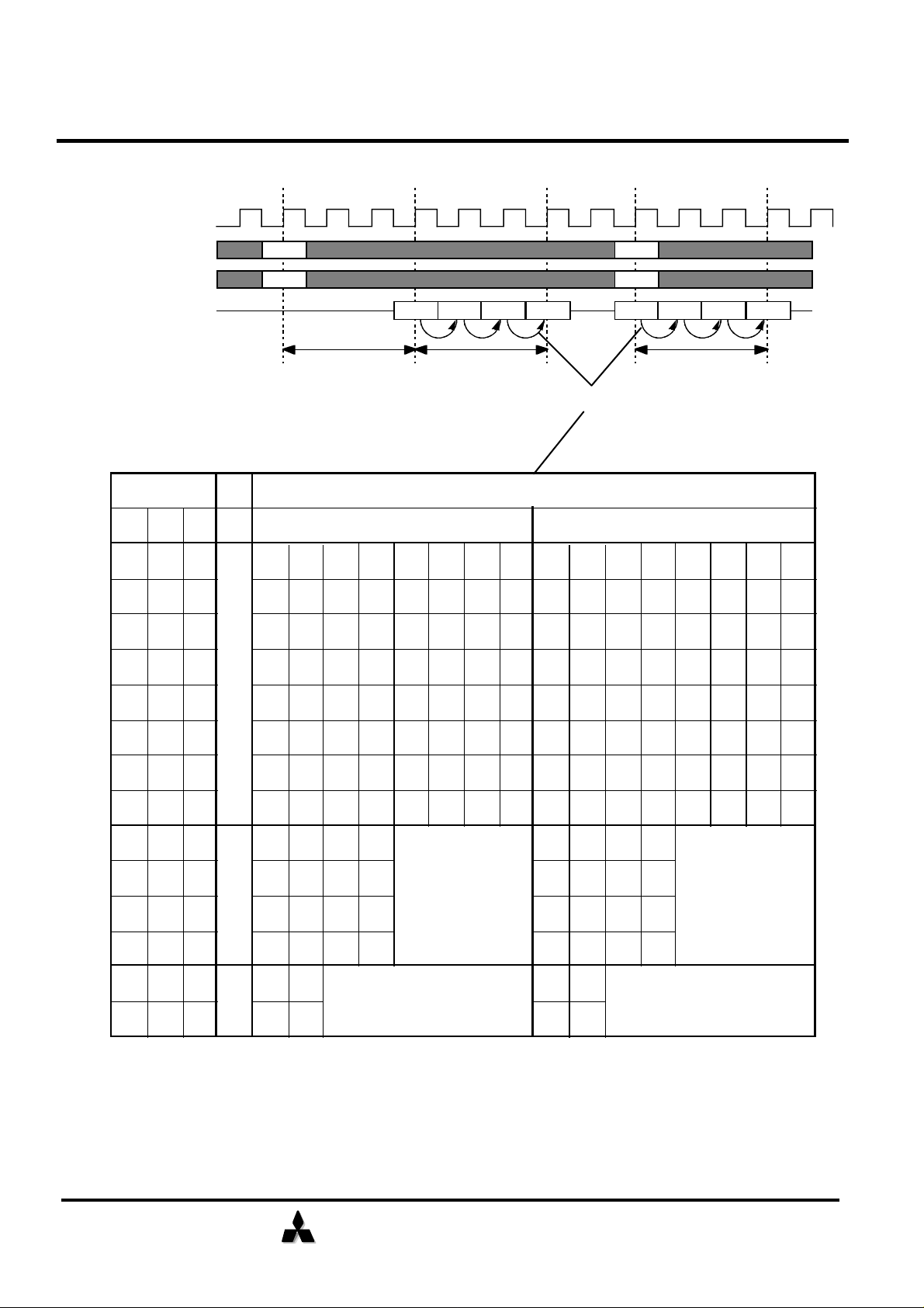
/CAS latency, CL, is used to synchronize the first output data with the CLK frequency, i.e., the
READ
READ
Oct. '99
M2V64S20BTP-6 (4-BANK x 4194304-WORD x 4-BIT)
MITSUBISHI LSIs
M2V64S30BTP-6 (4-BANK x 2097152-WORD x 8-BIT)
M2V64S40BTP-6 (4-BANK x 1048576-WORD x 16-BIT)
[ /CAS LATENCY ]
speed of CLK determines which CL should be used. First output data is available after CL
cycles from READ command.
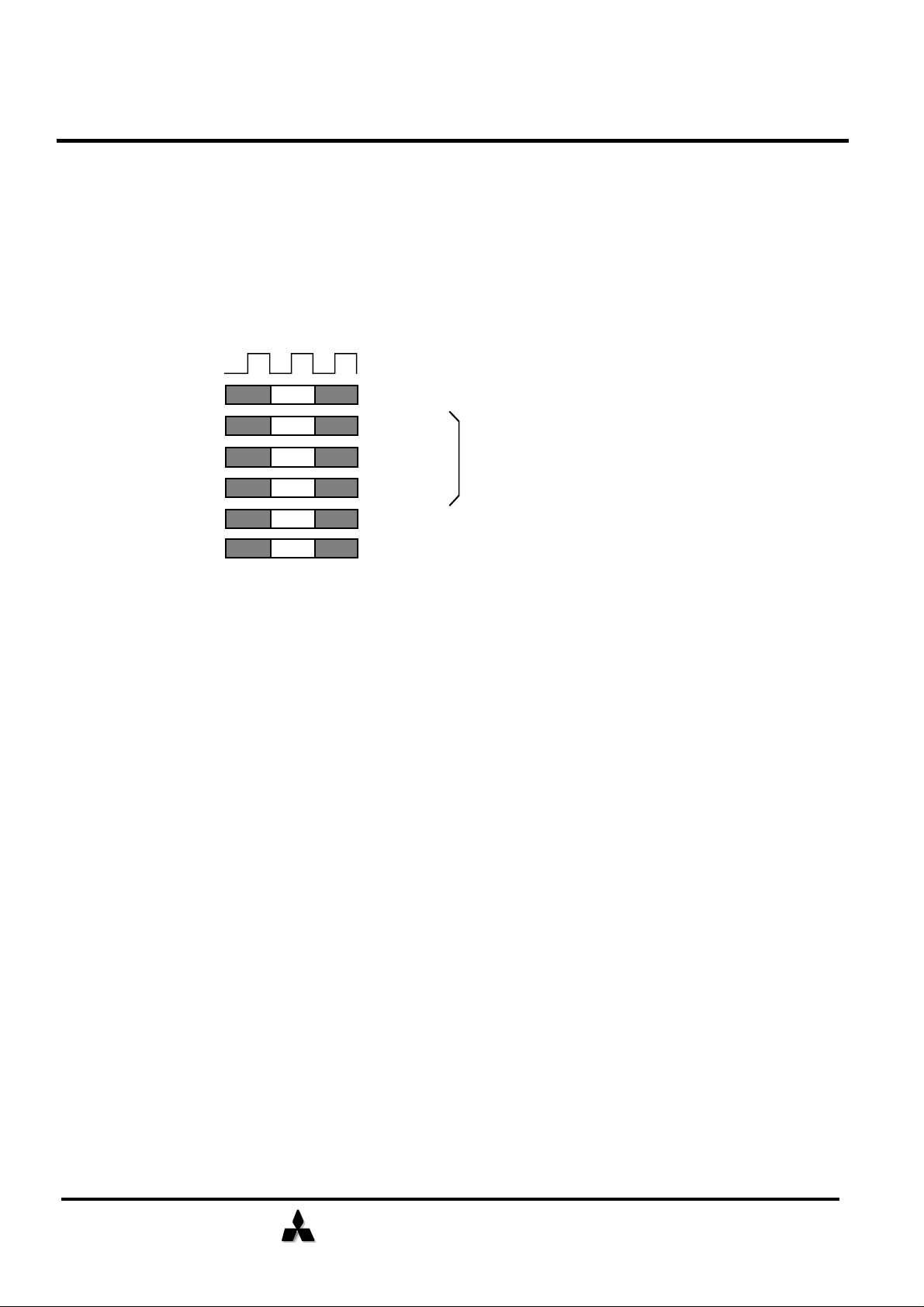
/CAS Latency Timing(BL=4)
CLK
Command
Address
DQ Q0 Q1 Q2 Q3
DQ Q0 Q1 Q2 Q3
ACT
X
tRCD
Y
CL=2
CL=2
CL=3
CL=3
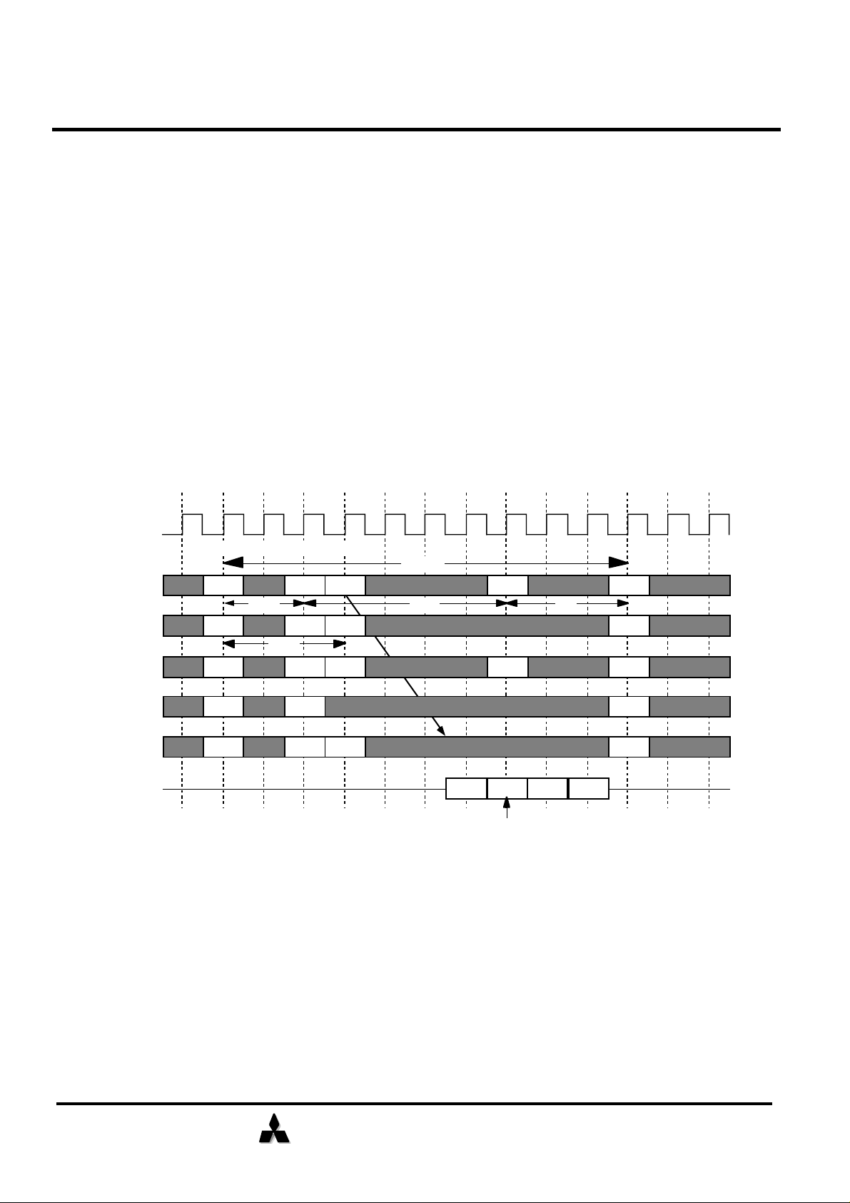
[ BURST LENGTH ]
The burst length, BL, determines the number of consecutive writes or reads that will be
automatically performed after the initial write or read command. For BL=1,2,4,8, full page the
output data is tristated (Hi-Z) after the last read. For BL=FP (Full Page), the TBST (Burst
Terminate) command should be issued to stop the output of data.
Burst Length Timing( CL=2 )
tRCD
CLK
Command
Address
DQ Q0
DQ Q0 Q1
DQ Q0 Q1 Q2 Q3
DQ Q0 Q1 Q2 Q3
DQ Q0 Q1 Q2 Q3 Q4 Q5 Q6 Q7 Q8 Qm Q0 Q1
ACT
X Y
Q4 Q5 Q6 Q7
M2V64S20B : m=1023
M2V64S30B : m=511
M2V64S40B : m=255
BL=1
BL=2
BL=4
BL=8
BL=FP
Full Page counter rolls over
and continues to count.
14
MITSUBISHI ELECTRIC
PC133 SDRAM (Rev.0.5)
64M bit Synchronous DRAM
Oct. '99
CLK
MITSUBISHI LSIs
M2V64S20BTP-6 (4-BANK x 4194304-WORD x 4-BIT)
M2V64S30BTP-6 (4-BANK x 2097152-WORD x 8-BIT)
M2V64S40BTP-6 (4-BANK x 1048576-WORD x 16-BIT)
Command
Address
DQ
Initial Address
A2 A1 A0
0 0 0
0 0 1
0 1 0
0 1 1
1 0 0
CL= 3
BL= 4
BL
8
Read
Y
Q0 Q1 Q2 Q3
/CAS Latency Burst Length Burst Length
Burst Type
Column Addressing
Sequential Interleaved
0 1 2 3 4 5 6 7 0 1 2 3 4 5 6 7
1 2 3 4 5 6 7 0 1 0 3 2 5 4 7 6
2 3 4 5 6 7 0 1 2 3 0 1 6 7 4 5
3 4 5 6 7 0 1 2 3 2 1 0 7 6 5 4
4 5 6 7 0 1 2 3 4 5 6 7 0 1 2 3
Write
Y
D0 D1 D2 D3
1 0 1
1 1 0
1 1 1
- 0 0
- 0 1
- 1 0
- 1 1
- - 0
- - 1
5 6 7 0 1 2 3 4 5 4 7 6 1 0 3 2
6 7 0 1 2 3 4 5 6 7 4 5 2 3 0 1
7 0 1 2
0 1 2 3
1 2 3 0
4
2 3 0 1
3 0
0 1
2
1 0
3 4 5 6 3 2 1 0
1 2
7 6 5 4
0 1 2 3
1 0 3 2
2 3 0 1
3 2
0 1
1 0
1 0
15
MITSUBISHI ELECTRIC
PC133 SDRAM (Rev.0.5)
64M bit Synchronous DRAM
OPERATIONAL DESCRIPTION
Oct. '99
M2V64S20BTP-6 (4-BANK x 4194304-WORD x 4-BIT)
M2V64S30BTP-6 (4-BANK x 2097152-WORD x 8-BIT)
M2V64S40BTP-6 (4-BANK x 1048576-WORD x 16-BIT)
MITSUBISHI LSIs
BANK ACTIVATE
The SDRAM has four independent banks. Each bank is activated by the ACT command with
the bank addresses (BA0,1). A row is indicated by the row addresses A11-0. The minimum
activation interval between one bank and the other bank is tRRD.The number of banks which
are active concurrently is not limited.
PRECHARGE
The PRE command deactivates the bank indicated by BA0,1. When multiple banks are active,
the precharge all command (PREA, PRE + A10=H) is available to deactivate them at the same
time. After tRP from the precharge, an ACT command to the same bank can be issued.
Bank Activation and Precharge All (BL=4, CL=3)
CLK
tRCmin
Command
A0-9
A10
A11 Xa Xb Xb
BA0,1
DQ
ACT
Xa
Xa
00
tRRD
tRCD
ACT
Xb
Xb
01
READ
Y
0
00
PRE
tRAS tRP
1
Qa0 Qa1 Qa2 Qa3
Precharge all
ACT
Xb
Xb
01
READ
After tRCD from the bank activation, a READ command can be issued. 1st output data is
available after the /CAS Latency from the READ, followed by (BL -1) consecutive data when the
Burst Length is BL. The start address is specified by A9-0(x4), A8-0(x8), A7-0(X16), and the
address sequence of burst data is defined by the Burst Type. A READ command may be
applied to any active bank, so the row precharge time (tRP) can be hidden behind continuous
output data by interleaving the multiple banks. When A10 is high at a READ command, the autoprecharge (READA) is performed. Any command (READ, WRITE, PRE, ACT) to the same bank
is inhibited till the internal precharge is complete. The internal precharge starts at BL after
READA. The next ACT command can be issued after (BL + tRP) from the previous READA.
16
 Loading...