

Page 1
Service
PM7003 /
F N/K1SG/N1SG
/N1B
Manual
STANDBY
POWER ONOFF
SECTION PAG E
1. TECHNICAL SPECIFICATIONS ........................................................................................... 1
2. ALIGNMENTS ....................................................................................................................... 2
3. SERVICE MODE ................................................................................................................... 4
4. PROTECTION MODE ........................................................................................................... 5
5. WRITING MAIN MICROPROCESSOR PROCEDURE ......................................................... 7
6. WIRING DIAGRAM .............................................................................................................25
7. BLOCK DIAGRAM ..............................................................................................................27
8. SCHEMATIC DIAGRAM ...................................................................................................... 29
9. PARTS LOCATION .............................................................................................................. 37
10. EXPLODED VIEW AND PARTS LIST ................................................................................. 47
11. MICROPROCESSOR AND IC DATA ................................................................................... 51
12. ELECTRICAL PARTS LIST ................................................................................................. 56
13.
ABOUT REPLACE THE MICROPROCESSOR WITH A NEW ONE ...............................71
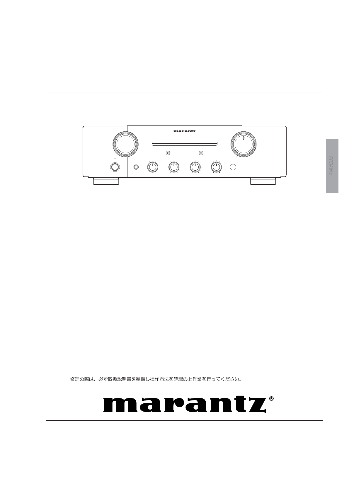
INTEGRATED AMPLFIER PM7003
INPUT SELECTOR VOLUME
PHONES
POWER AMP DIRECT
SPEAKERS
A
B
OFF
A+B
-
AUXDVD MUTERECORDER1TUNERPHONO CD
SOURCE DIRECT
TREBLEBASS
+
+
-
TABLE OF CONTENTS
Integrated Amplifier
BALANCE
RL
MAXMN
P 7 03
Please use this service manual with referring to the user guide ( D.F.U. ) without fail.
PM7003
Part no. 90M24AJ855010
First Issue 2008.07
MZ
Page 2
MARANTZ DESIGN AND SERVICE
Using superior design and selected high grade components,
Only original
MARANTZ
parts can insure that your
MARANTZ
MARANTZ
product will continue to perform to the specifications for which
company has created the ultimate in stereo sound.
it is famous.
Parts for your
MARANTZ
ORDERING PARTS :
equipment are generally available to our National Marantz Subsidiary or Agent.
Parts can be ordered either by mail or by Fax.. In both cases, the correct part number has to be specified.
The following information must be supplied to eliminate delays in processing your order :
1. Complete address
2. Complete part numbers and quantities required
3. Description of parts
4. Model number for which part is required
5. Way of shipment
6. Signature : any order form or Fax. must be signed, otherwise such part order will be considered as null and void.
USA
MARANTZ AMERICA, INC
100 CORPORATE DRIVE
MAHWAH, NEW JERSEY 07430
USA
JAPAN
D&M Holdings Inc.
D&M BUILDING, 2-1 NISSHIN-CHO,
KAWASAKI-KU, KAWASAKI-SHI,
KANAGAWA, 210-8569 JAPAN
EUROPE / TRADING
D&M EUROPE B. V.
P. O. BOX 8744, BUILDING SILVERPOINT
BEEMDSTRAAT 11, 5653 MA EINDHOVEN
THE NETHERLANDS
PHONE : +31 - 40 - 2507844
FAX : +31 - 40 - 2507860
CANADA
D&M Canada Inc.
5-505 APPLE CREEK BLVD.
MARKHAM, ONTARIO L3R 5B1
CANADA
PHONE : 905 - 415 - 9292
FAX : 905 - 475 - 4159
KOREA
D&M SALES AND MARKETING KOREA LTD.
CHUNG JIN B/D., #1001,
53-5, WONHYORO 3 GA, YONGSAN-GU,
SEOUL, 140-719, KOREA
PHONE : +82 - 2 - 323 - 2155
FAX : +82 - 2 - 323 - 2154
CHINA
D&M SALES AND MARKETING SHANGHAI LTD.
ROOM.808 SHANGHAI AIRPORT CITY TERMINAL
NO.1600 NANJING (WEST) ROAD, SHANGHAI,
CHINA. 200040
TEL : 021 - 6248 - 5151
FAX : 021 - 6248 - 4434
NOTE ON SAFETY :
Symbol Fire or electrical shock hazard. Only original parts should be used to replaced any part marked with symbol .
Any other component substitution (other than original type), may increase risk of fire or electrical shock hazard.
安全上の注意:
がついている部品は、安全上重要な部品です。必ず指定されている部品番号のものを使用して下さい。
SHOCK, FIRE HAZARD SERVICE TEST :
CAUTION : After servicing this appliance and prior to returning to customer, measure the resistance between either primary AC
cord connector pins ( with unit NOT connected to AC mains and its Power switch ON ), and the face or Front Panel of product and
controls and chassis bottom.
Any resistance measurement less than 1 Megohms should cause unit to be repaired or corrected before AC power is applied, and
verified before it is return to the user/customer.
In case of difficulties, do not hesitate to contact the Technical
Department at above mentioned address.
080702MZ
Page 3
1. TECHNICAL SPECIFICATIONS
Power output
(20 Hz – 20 kHz sim
8 Ω load ..............................................................70 W x 2
4 Ω load ...........................................................100 W x 2)
Total harmonic distortion
(20 Hz – 20 kHz simultaneous drive of both channels, 8 Ω load)
.........................................................................0.02 %
Output band width (8 Ω load, 0.05 %)
............................................................. 5 Hz – 60 kHz
Frequency response (CD, 1 W, 8 Ω load)
.................................................5 Hz – 100 kHz ±3 dB
Dumping factor (8 Ω load, 20 Hz – 20 kHz) ......................100
Input sensitivity/Input impedance
PHONO (MM) ................................................2 mV/47 kΩ
CD, LINE, TUNER, AUX/DVD, RECORDER
.............................................................200 mV/20 kΩ
MAIN IN .........................................................1.6 V/20 kΩ
Output voltage/Output impedance
PRE OUT .......................................................1.6 V/600 Ω
Maximum allowable PHONO input level (1 kHz)
MM ....................................................................... 100 mV
RIAA deviation (20 Hz ~ 20 kHz) ......................... ±0.5 dB
S/N (IHF-A, 1 W, 8 Ω load)
PHONO (MM)) ........................................................ 85 dB
CD, LINE, TUNER, AUX/DVD, RECORDER ........... 88 dB
POWER AMP DIRECT IN ..................................... 106 dB
Tone control
Bass (50 Hz) ......................................................... ±10 dB
Treble (20 kHz) ...................................................... ±10 dB
Power requirement
[F] .....................................................AC 100 V, 50/60 Hz
[N] ..........................................................AC 230 V, 50 Hz
Power consumption
EN60065/J60065 ....................................................200 W
Standby power consumption .........................................0.3 W
ultaneous drive of both channels)
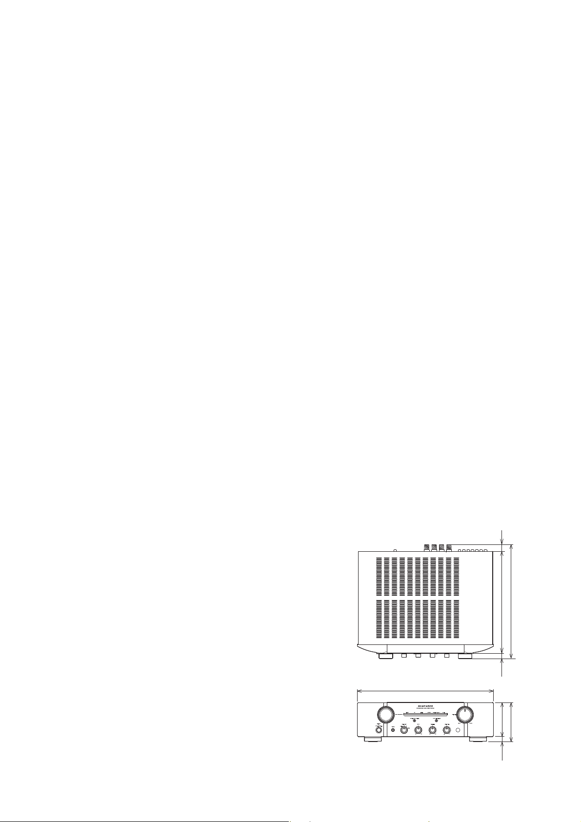
DIMENSIONS (unit : mm)
Accessories
Remote controller (RC003PM)........................................1
AAA batteries ..................................................................2
Detachable AC power cable ............................................1
Maximum outer dimensions (Amplifier)
Width ....................................................................440 mm
Height ..............................................................126.8 mm
Depth ................................................................... 368 mm
Weight (Amplifier) .................................................10.5 kg
22
368
328.5
17.5
440
16.3
110.5
126.8
1
Page 4
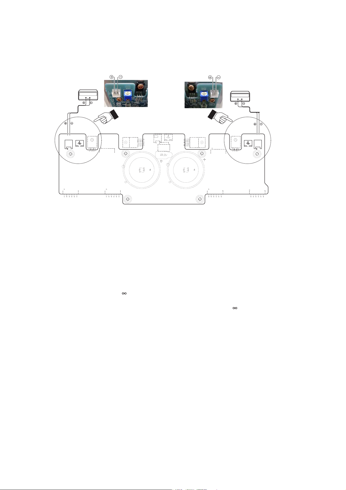
2. ALIGNMENTS
2. ALIGNMENTS
1. Idling Current Alignment
Digital Voltmeter
V
L ch
ADJ
T.P.
R707
J707
P701
Adjustment Procedure
Set the power voltage to rated voltage for this adjustment.
Adjust the Idling Current with the variable resistor R707 1.
and R708 on the PWB P701.
Turn off the power.2.
"+" of Connect Digital Voltage is connected to the No. 1 3.
pin and connected "-" to No. 2 pin of J707.
"+" of Connect Digital Voltage is connected to the No. 1 4.
pin and connected "-" to No. 2 pin of J708.
Before turning on the power, R707 and R708 have been 5.
counter clockwise turned with the adjustment driver.
Turn on the power, VOLUME is set as -6.
After 2 minutes.7.
With seeing the digital voltage meter turn the variable
resister clockwise slowly to adjust the idling current.
Idling adjustment with R707 (R708).
s 4URN 2 2 CLOCKWISE TO INCREASE THE IDLING
current.
s 4HE ADJUSTMENT VALUE OF IDLING CURRENT IS
5 mV(25 mA) ± 0.5 mV(2.5 mA) each.
After 8 minutes.8.
Repeat the same procedure as 7.
s 4HE ADJUSTMENT VALUE OF IDLING CURRENT IS
13.4 mV(67 mA) ± 0.5 mV(2.5 mA) each.
Adjustment is completed.
Remove connection cable, attach the top cover.9.
NOTE : Idling current decreases with the temperature rise
inside the unit, and it is set to 10 mV (50 mA) of
setting value in about 30 minutes after turn on the
power.
.
1. アイドリング電流調整
Digital Voltmeter
V
R ch
ADJ
T.P.
R708
J708
調整手順
調整時は必ず電源電圧を定格電圧に合わせてください。
P701基板上の半固定抵抗R707とR708でアイドリング電流1.
を調整します。
電源を
OFFします。2.
P701
基板のJ707にデジタルボルトメーターを接続します。3.
デジタルボルトメーターはJ707の1番ピン(丸印側)を"+"、
2
番ピンを"-"に接続します。
P701基板のJ708にデジタルボルトメーターを接続します。4.
デジタルボルトメーターはJ708の1番ピン(丸印側)を"+"、
2
番ピンを"-"に接続します。
電源を投入する前に半固定抵抗
イバーで反時計方向に回しきってください。
電源を投入しボリュームを
電源を投入後
P701
2分経過後。7.
基板のJ707(J708)に接続したデジタルボルトメー
ターの電圧値を監視しながら、半固定抵抗
をゆっくりと時計向に回してください。
s R707と R708を時計方向に回すとアイドリング電流が増加
します。
s アイドリング電流の調整値はそれぞれ
"5 mV(25 mA) ± 0.5 mV(2.5 mA)"にします。
さらに
8分経過後。8.
上記7.の手順でもう一度調整します。
s アイドリング電流の調整値はそれぞれ
"13.4 mV(67 mA) ± 0.5 mV(2.5 mA)"にします。
以上で調整は完了です。
デジタルボルトメーターの接続を外し、トップカバーを取
9.
付けます。
注意
: 調整終了後トップカバーを取付けるとセット内部の温度
上昇に伴いアイドリング電流が減少し、電源投入後約
分で設定値の"10 mV(50 mA)"になります。
R707とR708を、調整ドラ5.
-6. にしてください。
R707(R708)
30
2
Page 5
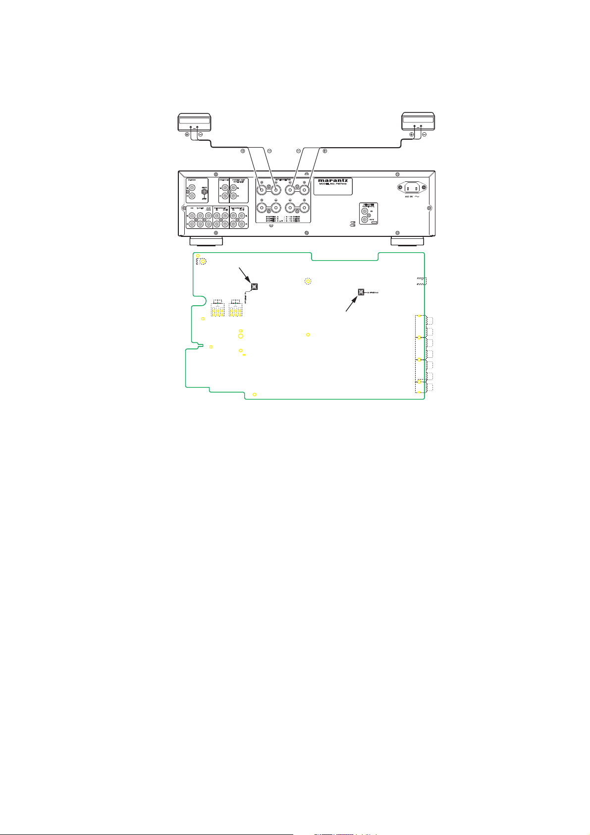
2. DC Offset Voltage Adjustment
Digital Voltmeter Digital Voltmeter
2. DC Offset Voltage Adjustment
P101
V
R ch
N
R639
SYSTEM A
RL
SYSTEM B
Y A
B
R640
L ch
N
V
Adjustment Procedure
Set the power voltage to rated voltage for this adjustment.
Before turning on the power, Insert Digital Voltage Meter 1.
between the SPEAKERS SYSTEM A (L CH) "+" and "-".
Insert Digital Voltage Meter between the SPEAKERS
SYSTEM A (R CH) "+" and "-".
Adjust the VOLUME to MIN.2.
Turn on the power. Then turn the SPAKERS knob to A. 3.
Adjustment is started immediately after a speaker relay
turns on.
First L CH is adjusted. 4.
The variable resistor R639 on P101 is turned with
adjustment driver, and the Digital Voltage Meter is
adjusted to "0 mV ± 3 mV".
Then, R CH is adjusted. 5.
The variable resistor R640 on P101 is turned with
adjustment driver, and the Digital Voltage Meter is
adjusted to "0 mV ± 3 mV".
NOTE : DC offset voltage drops when turn the semi-fixed
resistor (R639 and R640) clockwise. DC offset
voltage rises when turn the semi-fixed resistor unclockwise. Please turn it slowly, because value of
Digital Voltage Meter changes slowly.
Although after-adjustment DC offset voltage has some 6.
change, Please check that the range of DC offset voltage
between L ch (R ch) "+" and L ch (R ch) "-" terminal of
SPEAKERS SYSTEM A is "0 mV ± 20 mV". CHART OF
FACTORY MODE
調整手順
調整時は必ず電源電圧を定格電圧に合わせてください。
電源を
ONする前にリアパネルのSPEAKERS SYSTEM A1.
のL CHおよび、R CHそれぞれの"+"端子と"-"端子間にデジ
タルボルトメーターを接続します。
ボリュームを
MINにセットします。2.
電源を投入し本体前面のSPEAKERSノブを回し、Aにしま3.
す。
スピーカーリレーがONした後に調整を開始します。
最初に
L CHを調整します。 4.
P101
基板の半固定抵抗R639を調整ドライバーで回し、L
CH
スピーカー出力端子に接続したデジタルボルトメーター
の電圧が"
次に
P101
CH
の電圧が"
注意
: 半固定抵抗(R639、R640)を時計回りに回すと、DCオ
0 mv ± 3 mV"以内になるように調整します。
R CHを調整します。 5.
基板の半固定抵抗R640を調整ドライバーで回し、R
スピーカー出力端子に接続したデジタルボルトメーター
0 mv ± 3 mV"以内になるように調整します。
フセット電圧は減少し、反時計回りに回すと増加しま
す。
DCオフセット電圧の値は非常にゆっくりと増減し
ますので、半固定抵抗はゆっくりと回してください。
調整後
DCオフセット電圧は多少の変動がありますが、 6.
SPEAKERS SYSTEM A
の
"+"端子と"-"端子間のDCオフセット電圧は"0 mV ± 20
mV"
の範囲であることを確認してください。
のL CHおよび、R CHそれぞれ
3
Page 6
3. SERVICE MODE
3. SERVICE MODE
Microprocessor (QU01) version check
Connect the mains cord into the unit.1.
Press the 2. POWER button with pressing the SOURCE
DIRECT button on the Unit.
The firmware version is displayed on the front LED.3.
(Display time is only for 3 seconds.)
Version : 8 4 2 1
The firmware version is displayed in the lighting position of
LED.
Ex. :
Light up RECORDER-2 [1 ], Version : 1
Light up RECORDER-2 [1 ] and AUX/DVD [4 ], Version : 5
Light up RECORDER-2 [1 ] and TUNER [8 ], Version : 9
Each LED light up then all LED light up.4.
Turn off the power to quit Service Mode. 5.
(The unit to the default status)
Microprocessor (QU01) version 確認
1.
本機に電源ケーブルを接続します。
SOURCE DIRECT2.
押します。
ボタンを押しながら、POWERボタンを
FIRMWAREのバージョンがLEDにて表示されます。 3.
(
表示は3秒間のみです)
MUTERECORDER 21PHONO CD TUNER AUX/DVD
LED
が点灯している箇所がバージョン表示です。
表示例:
点灯RECORDER 2 [
点灯RECORDER 2 [
点灯RECORDER 2 [1 ] and TUNER [
フロントパネルのLEDが順次点灯し、その後全点灯しま4.
す。
電源を切ると
(
本機は、各種設定された内容が初期化され、工場出荷時の
状態に戻ります
SERVICEモードが解除されます。 5.
1
], Version:1
1
] and AUX/DVD [4 ], Version:
)
8
], Version:
5
9
4
Page 7

4. PROTECTION MODE
Explanation of microprocessor (QU01) [PROT-1 (pin6) and
PROT-2 (pin7)].
[A] The PROT-1 (pin6) is the port to detect the following
abnormalities of the Power AMP
Detection of an abnormality in the DC offset voltage from 1.
the Speaker Output terminal.
If the voltage from the Speaker Output terminal exceeds
approximately 1.2V (DC), Q955 or Q956 will turn on and
the signal from the PROT-1 terminal will change to L from
H.
Detection of an abnormal current from the power 2.
transistors (Q713 ~ Q716).
If an electric current of over 7A flows in Q713 or Q715,
Q951, Q953 and Q957 turn on, and the signal from the
PORT-1 terminal will change to L from H.
If an electric current of over 7A flows in Q714 or Q716,
Q952, Q954 and Q957 turn on, and the signal from the
PORT-1 terminal will change to L from H.
Detection of an abnormal temperature of the Heat Sink.3.
If the temperature of the Heat Sink exceeds
approximately +110 degrees C, the posistor (R969) will
turn on Q958 and the signal from the PROT-1 terminal
will change to L from H.
4. PROTECTION動作について
マイコン(QU01)のPROT-1 (pin6)とPROT-2 (pin7)の説明。
[A] PROT-1 (pin6)は、パワーアンプの下記の異常動作を検出
するポートです
スピーカー出力端子の
出。
スピーカー出力端子が約1.2V (DC) を超えるとQ955もしく
は
Q956がONして、PROT-1端子が "H→L" になる。
パワートランジスタ
Q713
もしくはQ715に約7Aを超える電流が流れるとQ951,
Q953, Q957
がONして、PROT-1端子が "H→L" になる。
Q714もしくはQ716に約7Aを超える電流が流れると
Q952,Q954,Q957がONして、PROT-1端子が "H→L" にな
る。
ヒートシンクの異常温度を検出。
3.
ヒートシンクの温度が約110℃を超えると、ポジスター
(R969)によってQ958がONして、PROT-1端子が "H→L" に
なる。
1.〜 3.のいずれかの異常検出でPROT-1端子が "H→L" になる
と保護回路が動作して、
て、即座にスピーカーリレー
す。
DCオフセット電圧の異常電圧を検1.
(Q713〜Q716)の異常電流を検出。2.
SPK_OUT (pin10) を "L→H" にし
L751, L752, L753をOFFにしま
If any of the above three abnormalities is detected, the
signal from the PROT-1 terminal will change to L from H,
and the protection circuit will be activated, the signal from
the SPK_OUT (pin10) changing to H from L and the speaker
relays L751, L752 and L753 immediately turned off.
What this protection operation results in after this depends
on how long the signal from the PROT-1 has to remain L.
s )F THE 02/4 PIN RECOVERS TO ( WITHIN AS SHORT A
period of time as one second or less.
The MUTE indicator starts flickering, thereby indicates
that the protection circuit has come into operation and
automatically turns down the volume. The protection
circuit is deactivated after approximately 15 seconds,
so that readjusting the volume will allow normal use
of the unit again. This protection operation is intended
for the situation wherein the user has misused the unit
temporarily and automatically resets the unit while the
amp circuit is functioning properly.
s )F THE 02/4 PIN REMAINS , FOR MORE THAN ONE SECOND
The amp will be powered off by the P_ON (pin15)
changing to H from L and Power relay L852 turned off
Then, the STANDBY indicator flickers, thereby indicating
that an error has occurred. This protection operation is
intended for a failure in the amp circuit and immediately
turns the power off to avoid the risk of any damage.
Depending on how the user is handling the unit, this
operation may be performed no matter if the amp is
functioning properly.
PROTECTION動作はPROT-1端子が "L" になっている時
この
間によって、その後の動作が異なります。
s PROT-1 (pin6)が1秒以内の短時間の間に "H" に復帰した場
合。
MUTEインジケーターが点滅しPROTECTION動作になっ
たことを知らせ、自動的にボリュームを下げます。
約15秒後に保護回路が解除しますのでボリュームを再調整
すればそのまま使用することができます。
これは、ユーザーが一時的に使用法を誤った場合を想定し
た
PROTECTION動作で、アンプ回路は故障していない場
合に自動復帰する動作です。
s PROT-1 (pin6)が1秒以上 "L" になっている場合。
P_ON (pin15) を "H→L" にして電源リレー L852 をOFF
し、アンプの電源をシャットダウンします。
このときSTANDBYインジケーターが点滅し、異常が起き
たことを表示します。
これは、アンプ回路の故障を想定したPROTECTION動作
で、危険回避のため即座に電源を切る動作です。
ユーザーの使用状況によっては、アンプが故障していなく
てもこの状態になる可能性もあります。
アンプが故障しているかどうかを確認するには、一旦電源
を切り1分ほど待ってから電源SWを再投入します。
この操作で
電源
は、約
ターが点滅します。
電源を再投入しても
は、アンプ回路が故障していると考えられます。
PROTECTION動作が解除します。
SWを再投入してもPROT-1 (pin6)が "L" の異常状態の場合
3秒後に再びシャットダウンしてSTANDBYインジケー
PROTECTION動作が解除されない場合
SW
5
Page 8

To check if the amp is in order, switch off the unit and switch
it on again one minute later. This action will deactivate
the protection operation. If the PROT-1 (pin6) remains
"L", which constitutes an abnormality, the unit shuts down
approximately 3 seconds later and the STANDBY indicator
starts flickering.
If the protection operation will not be deactivated after the
power is turned on again, the amp circuit may be broken.
[B] The PROT-2 (pin7) is the port to detect abnormalities
of the power supply circuit.
Detection of an abnormality in the power amp power 1.
supply circuit.
This port monitors the midpoint voltage of the power amp
power supply between +48V and -48V. If the voltage at
the connection point of R801 and R802 exceeds DC
±1.2V, Q903 or Q904 will turn on to change the signal
from the PROT-2 (pin7) to L from H.
Detection of an abnormality in the preamp power supply 2.
circuit.
Q901 and Q902 monitor the midpoint voltage between
+28V and -28V. If the voltage at the connection point of
R905 and R906 exceeds DC ±1.2V, Q901 or Q902 will
turn on to change the signal from the PROT-2 (pin7) to L
from H
Detection of an abnormality in the function relay power 3.
supply circuit.
If the +24VL of the relay power supply receives an
electric current of over 80 mA, Q815 and Q901 will turn
on to change the signal from the PORT-2 (pin7) to L from
H.
If any of the above three abnormalities is detected, the signal
from the P_ON (pin15) terminal will be changed to L from
H, the power relay L852 will be turned off and the unit will
be shut down. Then, the STANDBY indicator flickers and
indicates that an abnormality has occurred.
[B] PROT-2 (pin7)は、電源回路の異常を検出するポートです
パワーアンプ用電源回路の異常を検出。
1.
パワーアンプ用電源の+48V と-48Vの中点電圧を監視
し、
R801とR802の接続点の電圧が約 ±1.2V(DC) を超え
ると、
Q903もしくはQ904がONしてPROT-2 (pin7)が "H
→L"
になる。
プリアンプ用電源回路の異常を検出。
2.
Q901
とQ902 はプリアンプ用電源の +28V と -28V の
中点電圧を監視し、
±1.2V(DC) を超えると、Q901もしくはQ902がONして
R905とR906の接続点の電圧が約
PROT-2 (pin7)が "H→L" になる。
ファンクションリレー用電源回路の異常を検出。
3.
リレー用電源の+24VL に約80 mAを超える電流が流れる
と、
Q815, Q901がONしてPROT-2 (pin7)が "H→L" にな
る。
1.〜 3. のいずれかの異常を検出すると、P_ON (pin15) を
"L→H" にして、電源リレー L852 をOFFしシャットダウンし
ます。このとき
きたことを表示します。
これは、アンプ回路もしくは電源回路の故障を想定した
STANDBYインジケーターが点滅し、異常が起
PROTECTION動作で、危険回避のため即座に電源を切る動作
です。
アンプ回路もしくは電源回路が故障しているかどうかを確認す
るには、一旦電源
入します。
この操作で
電源
SWを再投入してもPROT-2 (pin7)が "L" の異常状態の場合
は、約
3秒後に再びシャットダウンしてSTANDBYインジケー
ターが点滅します。
電源を再投入しても
は、アンプ回路もしくは電源回路が故障していると考えられま
す。
SWを切り1分ほど待ってから電源SWを再投
PROTECTION動作が解除します。
PROTECTION動作が解除されない場合
This protection operation is intended for a breakdown of the
AMP circuit or the power supply circuit and immediately shut
s off the power in order to avoid the risk of damage.
To check if the amp circuit or the power supply circuit is
broken, switch off the power and then switch it on again
one minute later. This action will deactivate the protection
operation.
If the RPOT-2 (pin7) remains L after the power is switched on
again, the unit will be shut down again three seconds later
with the STANDBY indicator flickering.
If the unit is powered on again and yet cannot get the
protection operation deactivated, the amp circuit or the
power supply circuit may be broken.
6
Page 9
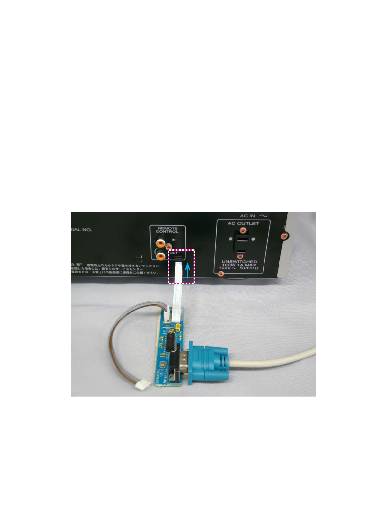
5. WRITING MAIN MICROPROCESSOR
PROCEDURE
Microprocessor needs writing software, when a
microprocessor (QU01) is replaced.
5. WRITING MAIN MICROPROCESSOR
PROCEDURE
QU01を交換したときはQU01へプログラムを書き込む必要が
あります。下記手順に沿って書き込みをしてください。
NECESSARY EQUIPMENT
s 7INDOWS 0# OR 80 WITH 3ERIAL 0ORT
s 23# #ABLE STRAIGHT TYPE 0IN FEMALE 0IN
female)
s #ONNECTION *)' -0-3*)'
s 7RITING 4OOL AND SOME FILES &LASH0ROGEXE ETC IN
TM86FH47pass folder)
s 7RITING DATA 0-?XXXXH
WRITING PROCEDURE
Disconnect the mains cord from the unit.1.
#ONNECT 23# ON THE CONNECTION *)' AND 3ERIAL 0ORT2.
of windows PC with RS-232C cable.
Connect FPC (upside contact) to the rear panel of the 3.
UNIT FROM CONNECTION *)'
必要機器
s Windows PC (2000またはXP、Serialポートつき)
s RS-232C
s
接続冶具(90M-PM11S1JI')
s
書き込み用ソフトウェア一式(FlashProg.exe、他)
s
書き込み用データ(PM7003_xxxx.h16)
ストレートケーブル(9Pinメス-9Pinメス)
書き込み手順
本機の電源ケーブルを抜きます。1.
Windows PC
で接続します。
本機のリアパネルに接続冶具の
して差し込みます。
のSerial Portと接続冶具をRS-232Cケーブル2.
FPCをコンタクト面を上に3.
Reconnect the mains cord to the unit. 4.
Put the "TM86FH47pass" folder into anywhere on your 5.
PC’s hard disc.
本機の電源ケーブルを差し込みます。4.
TM86FH47pass
にコピーします。
7
フォルダをWindows PCの任意のフォルダ5.
Page 10
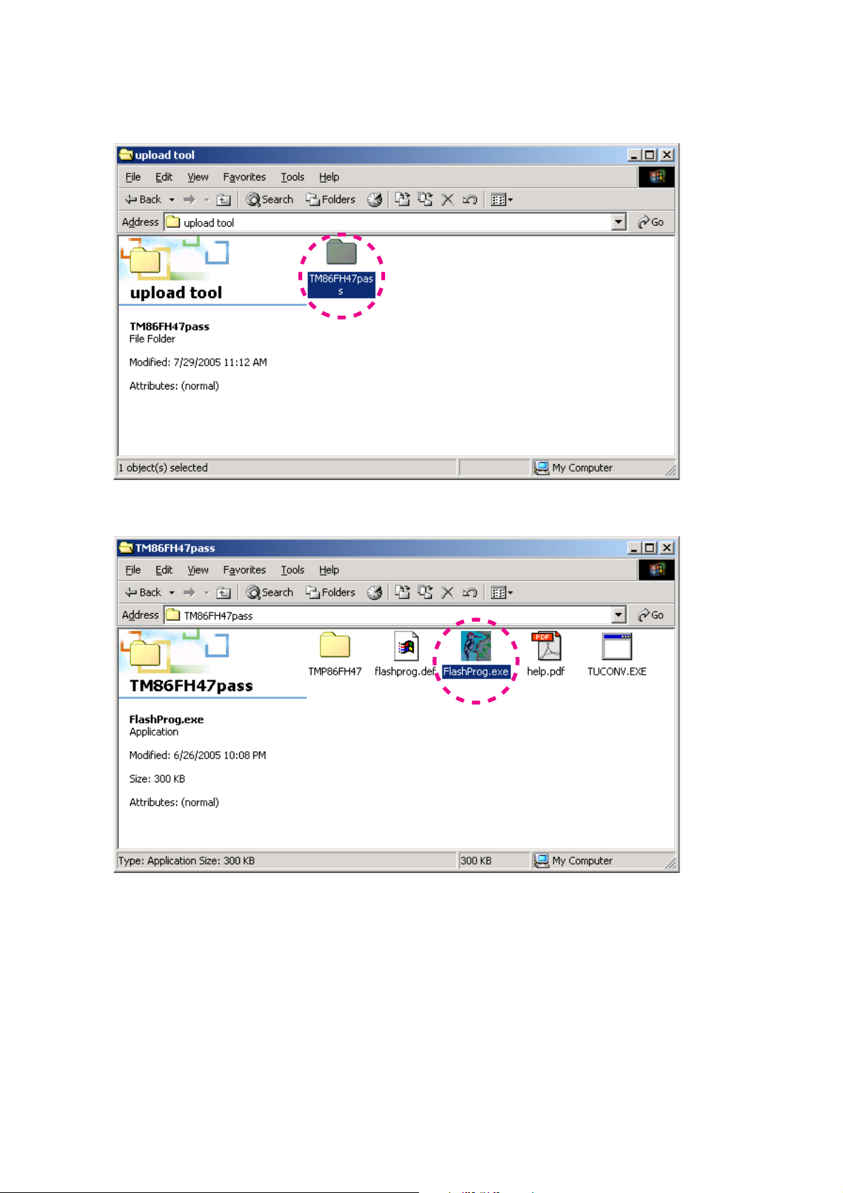
Double click the 6. TM86FH47pass folder.
TM86FH47pass6. フォルダをダブルクリックして開きます。
Double click 7. FlashProg.exe.
FlashProg.exe7.
をダブルクリックします。
8
Page 11
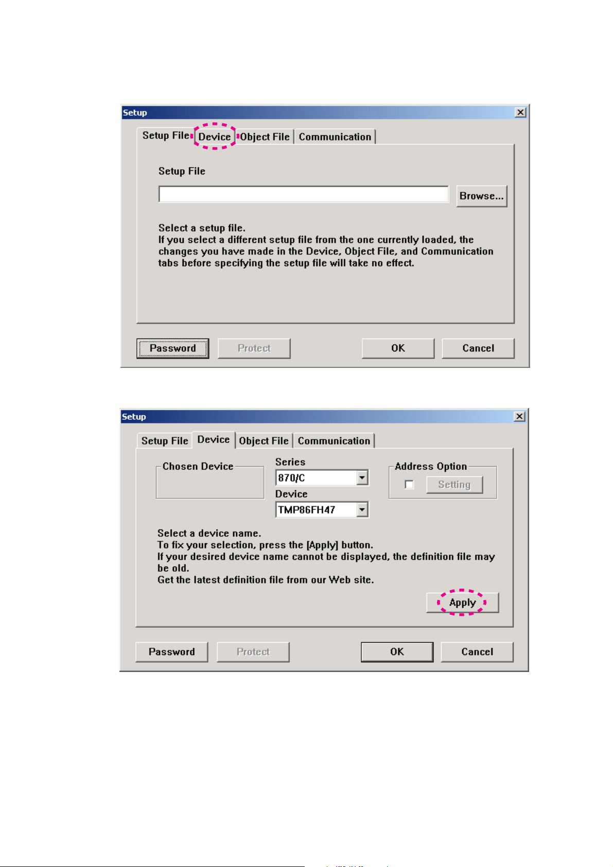
Click 8. Device.
Device8. をクリックします。
Click 9. Apply.
をクリックします。
Apply9.
9
Page 12

TMP86FH47 appear in Chosen Device.10.
Chosen DeviceにTMP86FH47が入力されます。10.
Click 11. Object File, and click Browse...
Object File11. をクリックし、Browse...をクリックします。
10
Page 13
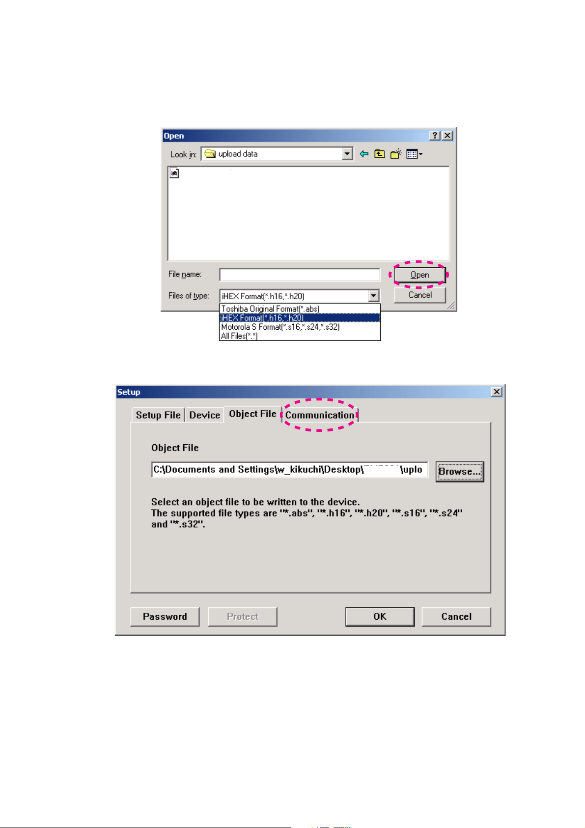
Choose 12. iHEX Fomat[*.h16,*.h20] in Files of type.
Choose writing data, and click Open.
PM7003_V09.h16
Files of typeから12. iHEX Fomat[*.h16,*.h20]を選び、書き込
み用データファイルを選択して
書き込むファイル名は変わることがあります。)
Openをクリックします。(
Click 13. Communication.
Communication13.
をクリックします。
PM7003
11
Page 14

Choose 14. COM port number in COM port.
Choose 9600 in Data Rate.
Click OK.
COM Portから接続する14. COM Port番号を選びます。
Data Rateから9600を選択します。
OKをクリックします。
When Setup window is closed, the tmp folder and 15.
FlashProg.ini file are created simultaneously.
NOTE : These are the original set-up configuration files for
that PC. They do not operate, if these files moved
to another PC. When you make it operate with other
PC, delete the tmp folder and the FlashProg.ini file
and redo a setup.
この時TMP86FH47passフォルダにtmpフォルダと15.
FlashProg.ini
注意
: これらは今設定したWindows PC独自の設定ファイルに
なります。他の
正しく動作しません。もし他の
ファイルが作成されます。
PCにこれらのファイルをコピーしても
PCで動作させる場合は
tmpフォルダとFlashProg.iniファイルは削除して設定を
やり直してください。
12
Page 15
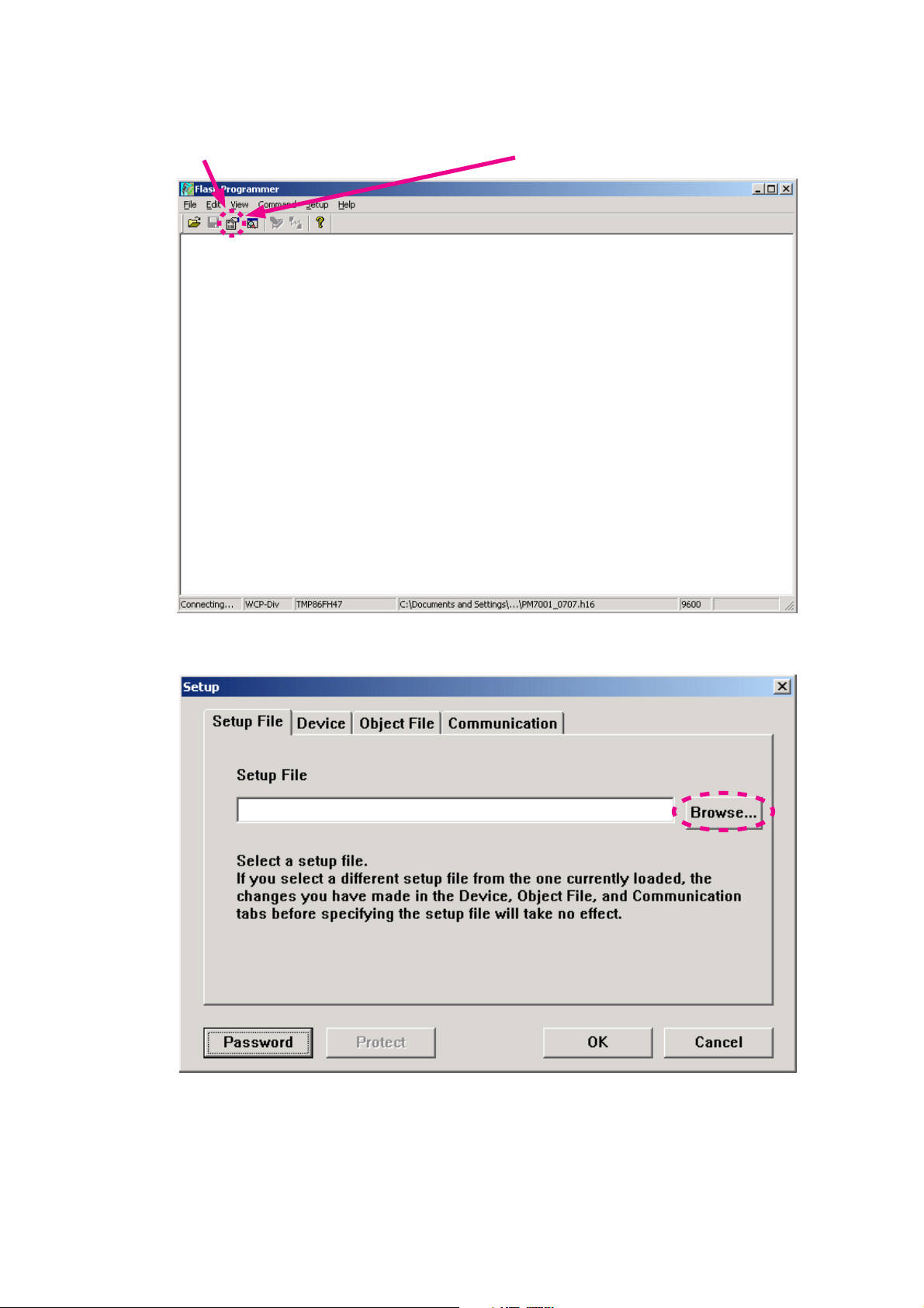
The Flash Programmer is launched.16.
Click setup icon.
setupが閉じ、Flash Programmerが立ち上がります。16.
setup
アイコンをクリックします。
Click 17. Browse....
Browse...17.
をクリックします。
13
Page 16
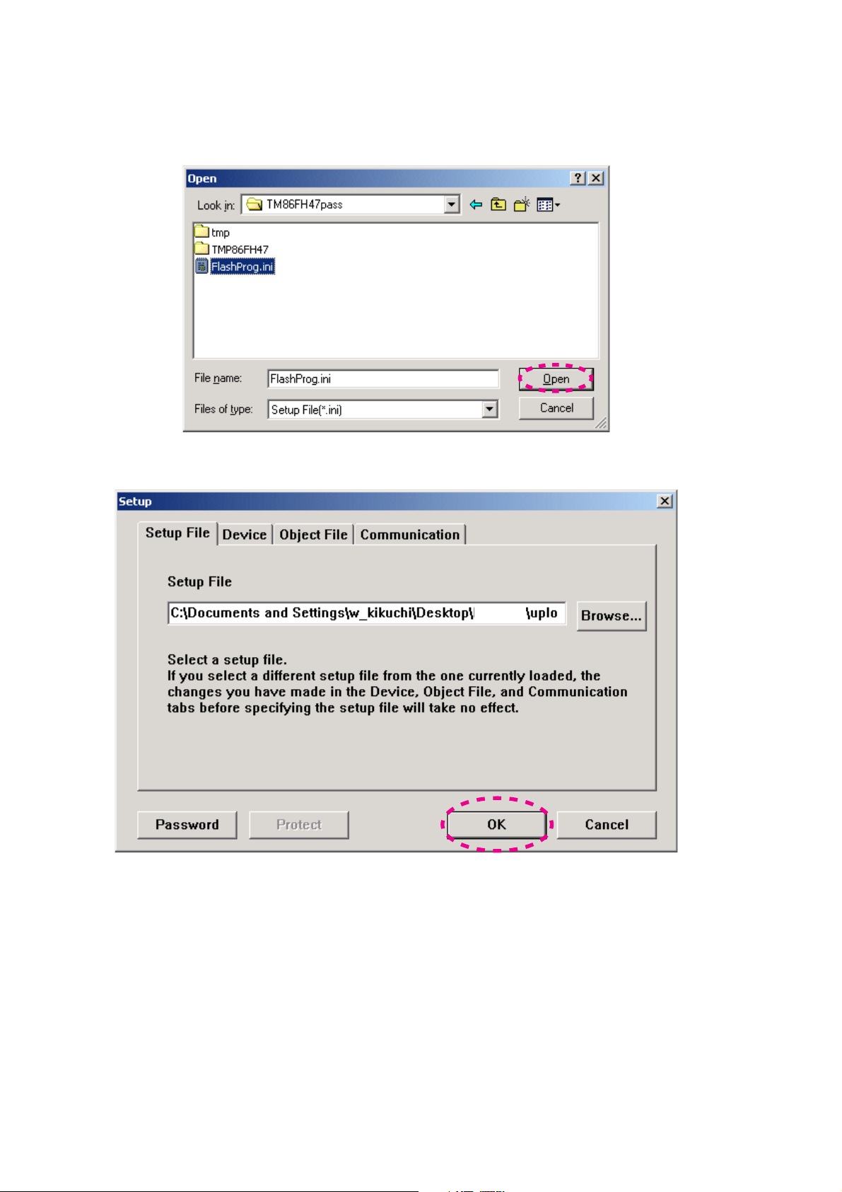
Choose 18. FlashProg.ini in TM86FH47pass folder, and
click Open.
Click 19. OK.
TM86FH47passフォルダから18. FlashProg.iniを選
び、
Openをクリックします。
をクリックします。
OK19.
PM7003
14
Page 17
Press the 20. POWER ON/OFF button, and turn on the unit.
Status indication at lower left in Flash Programming
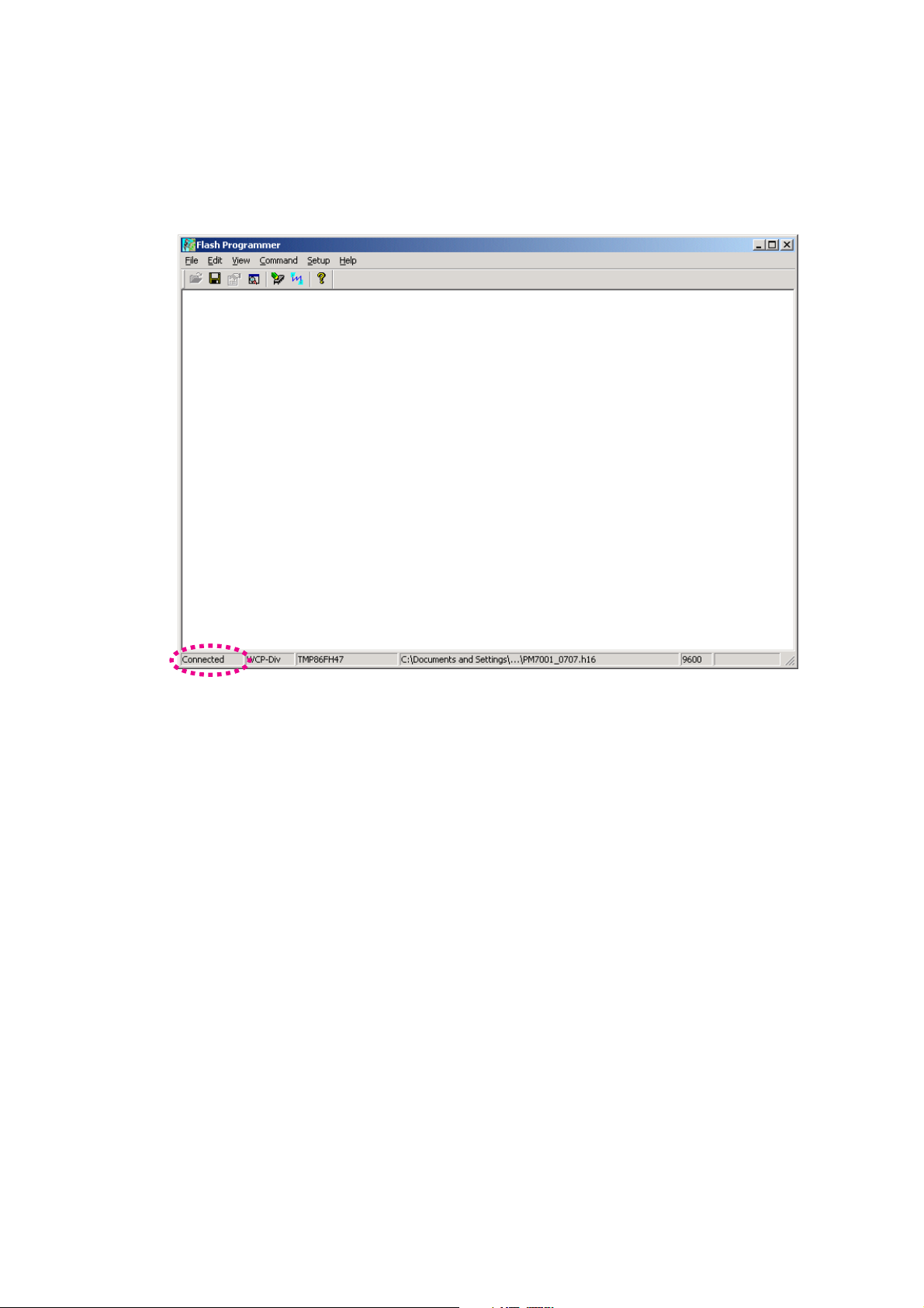
window is changed to "Connected" from "Connecting".
When it did not changed, check the connection of FPC or
RS-232C cable.
本機の電源スイッチをオンにします。20.
Flash Programming
ウィンドウの左下のステータスが
ConnectingからConnectedに変わります。もしConnected
に変わらないときは接続を確認してください。
15
Page 18
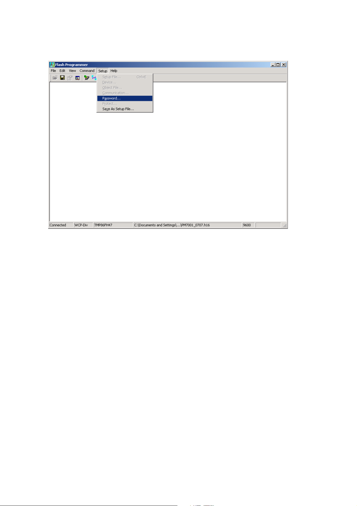
Select 21. Password in Setup.
Setup21. からPasswordを選びます。
16
Page 19
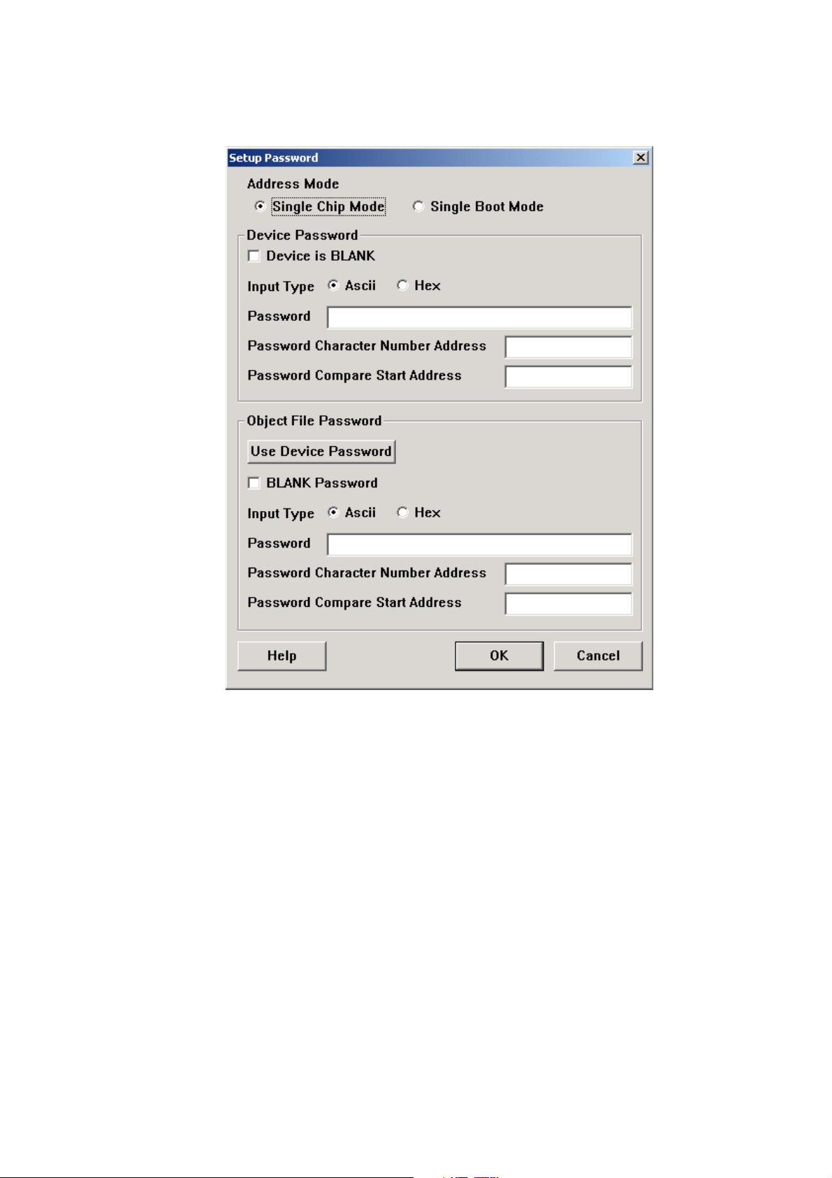
Setup Password opens.22.
Setup Password画面が開きます。22.
s When writing in a blank microprocessor
Refer to next page
s When writing (update) in the already written-in
microprocessor
Refer to 19 page
s
ブランクマイコンに書き込む場合は、次のページへ
s 既に書き込まれたマイコンに書き込む場合(アップデート)は
19ページへ
17
Page 20

When writing in a blank microprocessor
Check Single Boot Mode in Address Mode.
Setting in Device Password
Check Device is BLANK.
Check Hex in input type.
Since they are inputted automatically, please do
not change text box of "Password", "Password
Character Number Address" and “Password
Compare Start Address”.
Setting in Object File Password
Do not check BLANK password.
Check Hex in Input Type.
Type 0102030405060708 into Password.
Type 0xFF00 into Password Character Number
Address.
Type 0xFF01 into Password Compare Start
Address.
Click OK.
ブランクマイコンに書き込む場合
Address ModeからSingle Boot Modeにチェックを入れます。
Device Password内の設定
Device is BLANKのチェックボックスにチェックを
入れます。
input typeからHexにチェックを入れます。
Password、Password Character Number
Address
的に入力されますので変更しないでください。
、Password Compare Start Addressは自動
Object File Password内の設定
BLANK Passwordにはチェックを入れないでください。
Input TypeからHexにチェックを入れてください。
Passwordに0102030405060708を入力します。
Password Character Number Addressに0xFF00を
入力します。
Password Compare Start Addressに0xFF01を入力
します。
OKをクリックします。
18
Page 21

When writing in the already written-in microcomputer
(update)
. Check Single Boot Mode in Address Mode.
Setting in Device Password
Do not check Device is BLANK.
Check Hex in input type.
Type 0102030405060708 into Password.
Type 0xFF00 into Password Character Number
Address.
Type 0xFF01 into Password Compare Start
Address.
Setting in Object File Password
Do not check BLANK password.
Check Hex in Input Type.
Type 0102030405060708 into Password.
Type 0xFF00 into Password Character Number
Address.
Type 0xFF01 into Password Compare Start
Address.
Click OK.
既に書き込まれたマイコンに書き込む場合(アップデート)
Address Mode
す。
からSingle Boot Modeにチェックを入れま
Device Password内の設定
Device is BLANKにはチェックを入れないでください。
input typeからHexにチェックを入れます。
Passwordに0102030405060708を入力します。
Password Character Number Addressに0xFF00を
入力します。
Password Compare Start Addressに0xFF01を入力
します。
Object File Password内の設定
BLANK Passwordにはチェックを入れないでください。
Input TypeからHexにチェックを入れてください。
Passwordに0102030405060708を入力します。
Password Character Number Addressに0xFF00を
入力します。
Password Compare Start Addressに0xFF01を入力
します。
OKをクリックします。
19
Page 22

Auto Programming opens.23.
Auto Programmingの設定画面が開きます。23.
20
Page 23

Check 24. All Erase, Programming, Verify with SUM and
File Compare in Flash Memory Programming.
Check Manual in Recover Process by Programming
Error.
Click Start.
Flash Memory Programmingから24. All Erase,
Programming, Verify with SUM, File Compare
クを入れます。
にチェッ
Recover Process by Programming ErrorからManualにチ
ェックを入れます。
Startをクリックします。
21
Page 24

Writing data is written into the microprocessor (QU01).25.
メインマイコン(QU01)への書き込みが行われます。25.
Click 26. Yes, when writing is successful.
書き込みが成功すると下記のような画面が出ますので26. Yes を
クリックします。
22
Page 25

Click 27. Cancel.
Click 28. Cancel.
Cancel27. をクリックし終了します。
をクリックします。
Cancel28.
23
Page 26

Select the 29. Exit in File, and finish.
File29. からExitを選び終了します。
Press the 30. POWER ON/OFF button, and turn off the unit.
Disconnect each cable.
Check the software version.31.
Refer to "3. SERVICE MODE" on page 4.
本機の電源スイッチを切りケーブルを外します。30.
Software
4
のVersion確認をしてください。31.
ページの"3.SERVICE MODE"で確認します。
24
Page 27

6. WIRING DIAGRAM
PHONO AMP PWB
W202
P401
J281J282
W201
W401
W291
T0 WU01
W005
J331
J283
J901
JU02
J591
J592
J501
P591
VOLUME PWB
1234567
WU01
J593
P101
MAIN PWB
TO J591
J913
CHASSIS
W007
J755
T0 JU07
P751 (P971)
SPEAKER TERMINAL
J701W601
J709
W008
PWB
J751
J754
J702W602
P701
POWER STAGE PWB
J821
CHASSIS
J911 W951
J824J912
CHASSISCHASSIS
J811
W801
J801
WA01
WIRE ASSY
J792
P791
HEADPHONE PWB
W791
CHASSS
WA01
L001
MAIN TRANSFORMER
J855
W204
CHASSIS
P201
TONE PWB
W203
J201
JU06
PU01
U-COM PWB
JU01
J861
P851
STANDBY BWB
J864 J862J852
SOFT UPDATE PORT
W011
JU05
W181
P181
INPUT SELECTOR PWB
JU03
JU07
JU04
W191
P191
STANDBY LED PWB
TO J755
POWER SW PWB
CHASSIS
W003
J891
P891
25 26
J851
W002
J854
J853
J001
W001
AC CORD
Page 28

7. BLOCK DIAGRAM
PHONO
CD
TUNER
AUX / DVD
RECORDER 1
IN
RECORDER 2
IN
RECORDER 1
OUT
RECORDER 2
OUT
JAPAN VERSION ONLY
AC OUTLET
AC IN
CD DIRECT
BUFFER
FUSE
PRE OUT
RIAA
SOURCE DIRECT
CD
DIRECT
STANDBY
RELAY
POWER
ON/OFF
INPUT SERECTOR
FUSE
LINE BUFFER
REC OUT SELECTOR
REC BUFFER
MA N TRANS
SUB TRANS
VOLUME
NFB
±50V
±18V
24V
12V μ COM
MUTE
TREBLE
BALANCE
BASS
R CH
POWER AMP
PRE AMP
RELAY
5V
INDICATOR
5V
RELAY
POWER DETECT
PROTECTION
CONTROLLER NDICAT ON LED
EEPROM
I/R SENSOR
NFB
PROTECION
CIRCUIT
μ COM
RC5
STANDBY RELAY
FUNCTION RELAY
INPUT SELECTOR
RC5 IN/OUT
POWER AMP
DIRECT
SPEAKER A
SPEAKER B
SPEAKER B
SPEAKER B
HEADPHONE
(+)
( )
(+)
( )
2827
Page 29

8. SCHEMATIC DIAGRAM
P401 PHONO AMP PWB
PHONO GND
J002
J401
TPF301
EARTH
2
TPF 02
3
PHONO
TPF303
1
TPF304
4
J291
TPF305
2
TPF 06
3
PRE OUT
TPF307
1
TPF308
5
TPF 9
6
MAIN IN
4
TPF310
7
TPF311
WU01
R401R402
F 33
N K 100
R401
100k
R403
R404
100k
R402
220k 220k
R295
1k
220k 220k
R296
1k
TO SPK TERMNAL PWB
P591 VOLUME PWB
TPF251
3
TPF252
2
1
J591
TO MAIN PWB
164V
TPZ 01
8
5
0V
6
0V
C403
10u/50
C405
470u10
220p
R407
100k
R405
C401
82
R408
82
100k
220p
C402
R406
C406
470u/10
C404
10u/50
0V
2
0V
3
4
TPZ302
330p 330p
C296 C295
P791
HEADPHONE PWB
TPF331
W010
1
2
TPF 2 TPF3 4
J754
3
J792
C591
C592
07MQ ST L
J501
Q401
NJM2068DD
R409
Q401
NJM2068DD
164V
87
R591
10u/50
M
10u50
PF253
PF254
0V
7
82k
C407
0039u
C408
0039u
R410
82k
1
0V
R791
TPF333
10
R792
TO U COM PWB
4
L401
320uH320uH
132
EX03
JAMPER
220p
C419
01u
220p
C420
C421
EX04
JAMPER
EX03EX04
L402
F version only
3 4
220p
C291
01u
C297
R292 R291
220p220p 220p
C293C294 C292
01u
C298
R294 R293
NK version only
31
2
50k50k
R591R591
46
5
PF258
PF259
PF257
PF256
PF255
TPF260
J592
1 3
1234567
J593
R419
165V
10
C413
R413
TPZ303
10u/50
R417
100
68k
100
R411
C411
1000p
NC
47k
C415
R415
001u
C409
C410
001u
1000p
C412
68k
R412
R414
100
C417
220u25
NC
47k
C418
C416
R416
220u/25
R418
C414
100
10u/50
R420
10
TO MAN PWB
J331
W401
TPF312
1
+18V
TPF313
2
18V
TPF314
3
PH OUT L
TPF315
4
AGND
TPF316
5
PH OUT R
165V
W291
TPF317
1
PRE OUT R
TPF318
2
AGND
TPF319
3
PRE OUT L
4
5
6
MAIN IN R
AGND
MAIN IN L
TO MAIN PWB
J283
TPF320
TPF321
TPF322
EX07
220V
TPF293
TPF294
230V
EX06
12
W001
12
J001
12
21
W002
J851 J852
21 21
TPF261
L851
SUB TRANSFORMER
4
NC
2
1
P851 STANDBY BWB
P891 POWER SW PWB
S891
C891
470p
TPF601
J891
12
12
W003
21
TPF262
TPF264
TPF263
J858
250V
F852
315A
J859
TPZ205
21
J860
JAPAN VERSON ONLY
R851
TPZ208
TPF 95
D855
D851
1D3
1D3
PZ201
5
9
5 9 AC11 8V
D856
D852
1D3
1D3
D853
C853
001u
R857
1D3
TPZ207
TPZ202
1D3
D854
TPZ209
290V
TPF602
C861C862
3300UF
PZ2 1
A GND
3300UF
290V
TPZ210
C851
C863
TPZ20
4
001
001
1
F85
J857
J856
3
T63A/250V FOR JAPAN
2
T315A/250V FOR OTHER
L852
Q851
KTC3199
4
1
C852
10u50
TPZ203
A GND
102V
10k
R861
22
Q854
116V
TPZ 06
KTA1268
R860
1k
TPZ 3
R859
1k
C860
2200u25
NC
C854
1u50
TPZ 1
4
A GND
EX21
F
EX22
N
EX23
K
EX24
L
EX25
U
NK version only
J791
2
3
1
HEAD PHONE
W791
C792
C791
001u10001u
1
TPF335
EARTH
35V
35V
C855
D857
D1NJ10
D858
D1NJ10
D859
D1NJ10
D860
D1NJ10
TPZ 96
260V
C857
A GND
Q852
PQ050ES1MXPQ
N
115V
10u50
TPF292
1
J864
EARTH
PZ 12
Q853
NJM7805FA
N
220u35
POWER ON0 7V
POWER OFF0V
OUT
GND
R854
100k
A GND
J855
290V
290V
R855
12W1
G851
21
R856
12W1
068 4 7
1D3
1D3
1D3
D861
D863
D865
1D
1D3
3
D862
D866
1D3
D864
R858
260V
100k
C859
1u50
TPZ 97
L855
5V
OU
GND
C858
10u50
TPZ298
R853
R852
47k
A GND
L853
50 V
C856
10u50
L854
Q855
KRA102M
PF291
J862
TPF265
TPF266
TPF267
J854
TPF268
TPF269
TPF270
J853
TPF271
TPF272
47k
0 6V
5 0V
5 0V
5 0V
0 6V
0V
5 0V
5 0V
C864
01u
PF290
PF289
54321
CE
RXD
FOR SOFT UPDATE
W006
+28V
2
To MAN PWB
28V
1
J811
+24VL
AC210V
1
1
2
2
3
3
AC210V
L001
MAIN TRANSFORMER
3
1
4
2
2
1
1
TPF273
TPF274
47
01u
C865
R862
C866
01u
TPF277
0V
TPF278
TPF279
TPF280
TPF281
0V
TPF282
TPF283
TPF284
TPF285
TPF286
PF288
PF287
TXD
+5VL
D-GND
5
6
2
8
J863
1
IN
3
RC BUS
PF275
2
OUT
4
TPF27
6
J861
1
RC5
2
P DOWN
3
+5VD
4
P ON
5
+5VL
TO U COM PWB
6
D GND
JU01
7
W007
P OFF
8
CE4
9
RXD
1
TXD
29 30
Page 30

To PHONO AMP PWB
W401
PH OUT L
PH OUT R
CD
TUNER
AUX/DVD
IN
OUT
RECORDER1
IN
OUT
RECORDER2
+18V
18V
A-GND
J331
J301
J302
4
6
5
1
3
2
7
J303
4
6
5
1
3
2
7
J304
4
6
5
1
3
2
7
E 1
F
EX12
N
EX13
K
EX14
L
EX15
U
P101 MAIN PWB
1
+18V
2
18V
3
4
5
A-GND
1
100p100p
C303C304
3
01u
C301
2
4
N K verson only
NK vers on on y
C333C334
01u
C331
C335C336
01u
C332
C339
01u
C337
C341
01u
C342 C340
C338
01u
C346
C343
C347
01u
C348 C345
C344
TO TONE PWB
TO VOLUME PWB
J592
B 7P MQ-C
PH L
KTC3200
KTA1268
0V
0V
KTC3200KTA1268
165V
C311C312
-165V
Q313
C353
C354
R387
10
A GND
R388
10
L
L
C309
22u/25
R323
10
100k100k
R321R322
220u25220u/25
A-GND
R324
10
C310
22u/25
R361
15k
22
R357R359R358R360
06 V
KTA1268
-06V
Q315
R363
222222
KTC3200
15k
330p
R362
330p
15k
06 V
KTA1268
Q314
06V
Q316
KTC3200
R364
15k
C
10u/50
R383R384
C386 C385
C3 4
220u25 220u/25
10u/50
R386
47
R385
R 1
0V
0V
0V
0V
0V
0V
0V
0V
-165V
CE
0V 16 5V
DATA
0V
CLK
0V
PH R
+18V
-18V
Q317
KTC3200
22
R365
C355
22
22u/25
R367
165V
Q319
KTA1268
Q318
KTC3200
-165V
22
R366
0V0V
C356
22
22u/25
R368
Q320
KTA1268
165V
8
1
NJM206
0V
100k100k
7
NJM206
0V
-165V
47
Q391
LC78212
0V
1
PH L
0V
2
CD L
0V
3
TU L
4
SL L
5
DV L
6
R1 L
7
R2 L
8
SL L
9
R1 LO
10
R2 LO
11
RO L
12
VEE
13
CE
14
DATA
15 16
CLK VSS
+24VL
10
R325
1345
301
CD DRECT
R371
10
100k
R369
C357
220u/25
A-GND
100k
R370
C358
220u25
R372
10
C381
3
0V
10u/50
Q381
2
100k100k
R381R382
0V
C382
5
0V
10u/50
Q381
6
0V
4
30
0V
PH R
R392
29
0V
CD R
22k22k
28
TU R
0V
27
0V
A GNDA-GND
SL R
0V
26
DV R
0V
25
R1 R
0V
24
R2 R
0V
23
SL R
0V
22
R1 RO
0V
21
R2 RO
0V
20
RO R
165V
19
VDD
18
RES
17
SET
0V
10k10u50
R393C393
D391
A-GND
R311
15k
22222222
R307R309
Q305Q307
06 V
KTA1268
Q301
0V
22 22
C305
10u/50
220k220k
R303R304
R301R302
C306
10u/50
220k
100p100p
R331
A GND
220k
R332
220k220k
100p100p
R333R334
A GND
220k
100p
R335
A GND
R339
560
220k 220k220k
100p
R337 R336R338
A GND
100p 100p
R340
560
220k
R341
A GND
220k220k
100p
R342R344
R345
560
220k
100p
R343
A GND
100p 100p
R346
560
R317R315
R305
06V
Q303
470
KTC3200
R313
15k
22k22k
330p330p
C307C308
R312
15k
R308
R306
TA1268
Q306Q308
06V
470
Q302
0V
22 22
R318 R316
06V
Q304
KTC3200
R310
4
15k
TU L
TU R
DV L
R355
C351
470
10u/50
27k
220k
R353
R351
DV R
R1 L
R1 R
R1 LO
R1 RO
R2 L
R2 R
R2 LO
R2 RO
27k
220k
R354
R352
R356
C352
470
10u/50
+18V
18V
PH
DV L
R1 L
R2 L
R1 LO
R2 LO
1234567
J501
A-GND
A-GND A-GND
VOL N LCH
VOL N RCH
VOL OUT LCH
VOL OUT RCH
D301
Q309
KRC102M
1k
R327
D-GND
1k
R328
+18V
-18V
PH R
TU RTU
DV R
R1 R
R2 R
R1 RO
R2 RO
CLK
DATA
CE
J901
L
18V
+18V
A-GND
W201
1
2
3R4
5
J281 J282
A-GND A GND
-18V
+18V
4
L281
SOURCE DREC
CD DRECT
ON 5V
OFF 0V
CD D
NCJUMPERNCJUMPER
R505
C501
22u/50
10k
R501
C503
NC
R507
C513
A-GND
R506
R504
C502
100
22u/50
10k
C504
R502
NC
C514
R508
A-GND
R819
+18V
47
168V
165V
C815
220u/25
A-GND
C816
220u25
-165V
R820
18V
47
168V
MUTE
PA_D
CD D
SO_D
1 34 678 10 11 12
TO TONE PWB
L
A-GND
W202
1R2
3
+24VL
10
R281
345121
L282
D281
MUTE
Q501
Q503
-06V
-12V
220u25 220u/25
220u25
Q502
-06V
-12V
220u25
Q813
18V
18V
470 470
Q814
12 V
06V
1 2V
0V
Q504
2SD1415
275V
275V
KTA1268
0V
KTC3200
SPL
KTA1268
KTC3200
Q811
Q812
R513
D501
R511 R509
D503
R515
R514
D502
R510
R512
D504
R516
KT 1267
C813
C814
KTC3199
SPK
SOURCE DIRECT
15k
0 6
22 22
06V
15k
15k
06V
22
22
06V
15k
470
R815
R811D811R813
268V
220u/25
R814D812R812
220u25
-268V
470
R816
C916
D-GND
TO U COM PWB
121198
SOURCE DREC
A GND
Q281
ON 5V
KRC102M
OFF 0V
D GND
SO D
470
R521C509
157V
157
Q509Q511
KTC3200KTA1268
Q513Q515
KTA1268KTC3200
Q505
151V
KTC3200
0V
22
R517
R519
R518
R520
JU02
W005
1M
R529
100p
22
0V
151V
Q507
KTA1268
470
R523
R543R545
470
R522
157V
157V
Q510
KTC3200
Q514
KTA1268
Q506
151V
KTC3200
0V
22
1M
100p
C510
R530
22
0V
151V
KTA1268
Q508
Q516
KTC3200
Q512
KTA1268
470
R524
R544
R546
330
290V
1k15k
33k33k
R905
15k
R906
C812 C811
22u50 22u50
1k
290V
01u
J811
123
+24V
-28V
+28V
109
100p
C507 C505
R547
100
C506
100p
C508
R548
100
180V
D813
D814
-180V
R818 R817
2SB1020
PROT_2
PROT_1
A GND
PRE-OUT-R
1
2
3
J283
+24VL +24VL
10
270
R290
R289
R283
R285
270
R287
470k470k
345
D282
L283
11198
TPZ28 TPZ27
R288
R286
270
MUTE
Q283
ON 5V
KRC102M
OFF 0V
D GND
MUTE
165V
15k15k
220
R525
R535R537
0 6V
Q517
Q525
KTA1268
KTC3200KTA1268
2222
R531R533
0V
0 6V
Q521
2222
R539R541
0V
0V
Q523
06V
KTC3200 KTA1268
Q527
Q519
06V
KTC3200
-157V-15 7V
220
R527
165V
330330
165V
15k22
220
R526
R536R532
0 6V
Q518
KTA1268
Q526
KTC3200
0V
KTA1268
Q522
22
R540
V
22
R542
0V
Q524
KTC3200
Q528
KTA1268
Q520
06V
KTC3200
-157V-15 7V
15k 22
220
R538 R534
R528
165V
330
+24VL
VOLTAGE DETECT
FOR PRE AMP
R901
10k
0V
10k
C901
1u/50
R902
D-GND
VOLTAGE DETECT
FOR POWER AMP
R903
0
10k
10k
C902
R904
10u50
D-GND
PRT 2
TO STANDBY PCB
J863
w006
PRE-OUT-L4MA N- N-R
270
POWER DRECT
R553
10
C511
22u/25
R555
10
R554
10
C512
22u/25
R556
10
R822
10
Q901
KTC3199
Q903
KTC3199
J821
EARTH
A GND
TO PHONO AMP PWB
MA N- N-L
5
6
A-GND
L284
POWER DRECT
ON 5V
OFF 0V
R551R503
JAMPER100
100k
R549
JAMPER
100k
R550
OVER CURRENT DETECT
FOR +24VL
R825
33k
R823
10k
R824
10k
Q902
PROTECT0V
NORMAL5V
Q904
C903
01u
A-GND
J912
W291
R284
345
121198
D GND
PA D
+18V
-18V
+18V
R552
18V
Q815
KTA1267
D GND
KTC3199
KTC3199
PROT_2
D-GND
L912
J913
EARTH EARTH
R659
490V
488V
481V
KTC3199KTC3199KTA1267KTA1267
R653R655
0V
481V
KTC3199
KTC3199
R654
R656
KTA1267
KTA1267
Q911
NORMAL0V
10 1/4W
R635
D609
11 V
D611
12V
47k
R639
11
06 V
D613
06V
470k
R641
D615
2222 100k100k
-11V
R645R647 D605D607 R649R651
0V
06V
Q625Q627
R637
47k 47k
2222
KTA1267KTC3199
0V
-06V
-06V
06V
R643
-12V
481V
-488V
11V
100k
R650
12V
06
V
D606
06V
R642
22
0V
R646
Q626
22
KTA1267
0V
22
KTC3199
Q628
0V
22
R648
-06V
-06V
R644
D608
-12V
100k
R652
481V
-488V
47k
R912
R911
260V
100k
KTA1267
+24VL
TO POWERSTAGE PWB
C609
TO J701
W601
220u/25
+47V
LOUT+
LOUT
4
-47V
5
100k
10 1/4W
10 1/4W
R636
D610
D614
470k
-11V
220u/25
100k
10 1/4W
C911
01u
NFB
R661
490V
490V488V
R660
47k
D612
47k
R640
D616
47k
R638
TO POWERSTAGE PWB
C610
TO J702
W602
+47V
ROUT+
3
ROUT
4
47V
5
NFB
R662
490V
TO POWERSTAGE PWB
W951
J911
D GND
1
PRT-1
2
PRT-2
3
+24VL
4
260V
D-GND
R667
470
R623
12 V
06 V
TA1268
0V
KTC3200
06V
0V
KTC3200 TA1268
Q916
R663
R611
D601
R607
R609
D603
R613
R665R664R666
A-GND
R612
R608 D602
R610R614
D604
A-GND
D-GND
PROTECT0V
NORMAL0 6V
KRC102M
R619
481V 48 1V
Q613
KTA1268
469V
-469V
Q615
KTC3200
R621
R631
470
R620
481V
Q614
KTA1268
469V
-469V
Q616
KTC3200
R622
R632
C913
D GND
Q918
260V
47k
R914
0V
Q917
KTC3199
68k
475
Q633Q629Q631Q635
18 V
1M1M150 150
680p
C607
R627R629
7
22
-18V
Q623 Q621
2SC2705 2SA1145
475V
Q619 Q617
KTC3200 KTA1268
-481V
-481V
R669
68k
470
R625
2W15 K
R668
150150
R624
68k
481V
475V
Q618
KTA1268
Q634
Q622
Q630
18V
1M
680p
C608
R628
R658
22
1M
R630
-18V
Q632
Q624
2SC2705
-475V
Q636
Q620
KTC3200 2SA1145
-481V
481V
R670
68k
470
R626
2W15 K
01u
C912
01u
Q912
KRC102M
D-GND
D912
PROTECT0V
NORMAL26V
PROT 1
SPL
27k27k27k27k
D617
NC
18k
Q609Q605
KTC3200KTC3200
06V
2222
0V
2222
TPZ63
R615R617
0V
0V
KTA1268
Q607
-06V
18k
Q611
619
KTA1268
NC
R633
100
D618
NC
18k
Q610
KTC3200
06V
Q606
22
KTC3200
0V
22
TPZ64
R616
0V
22
R618
KTA1268
2218k
Q608
-06V
Q612
D620
KTA1268
NC
R634
100
260V
PROTECT0V
NORMAL26V
Q914
KRC102MKRC10M
KT 67
R915
Q915
22k
D-GND
10
C613
22u/50
TPZ29TPZ30
D283
Q601
C601
R605
22u/25
100
Q284
KRC102M
220k
22k
R603
Q603
06V
F NC
N K 100P
12V
C615
22u/50
C605 C603
220u/63 220u/63
A-GND
C604
220u/63
C614
22u/50
12 V
C602
R606
22u/25
100
22k
220k
C612 C611
R602 R601
R604
Q604 Q602
06V
F NC
N K 100P
-12V
C616
22u/50
C606
220u/63
A-GND
R821
22
C821
220u/35
111
D911
26V
Q913
KRA102M
PROTECT26V
NORMAL0V
01u
C914
PROTECT0V
D-GND
NORMAL5V
22k
R913
D GND
SPK
3231
Page 31

P701 POWER STAGE PWB
J701
1
+47V
2
W601
PF192
LOUT+
3
PF193
LOUT
4
47V
5
PF195
NFB
TO MAN PWB
J702
1
+47V
W602
2
PF197
ROUT+
3
PF198
ROUT
4
47V
5
PF200
NFB
TO MAN PB
P751 (P971) SPEAKER TERMINAL PWB
TPZ 4
NORMAL0V
TPZ 3
C801
63V
15000u
C802
P GND
63V
15000u
47k
47k
R801
R802
D802
TPZ205
FCH10A15
FROM MAIN POWER TRANSFORMER
J801
G801
TPF2 7
1
068/4 7
TPZ 6
1
354V
AC
TPF2 8
2
GND
TPF2 9
3
354V
AC
TPZ207
12 12
D801
FRH10A15
TPZ208
0V
SPK L(+)
SPK R(+)
J709
TPF220
TPF221
TPF222
TPF223
P GND
P GND
PF224
1
W801
4
SPK L+
3
SPK L
2
SPK R
1
SPK R+
EARTH
W008
TO SPK TERMINAL PWB
J751
TO POWER STAGE PWB
490V
490V
Q713
2SC283
2SC2705
C705
2SA1145
06V
2SC3423
654321
J703
Q709
TPF 02
R725
06 V
TP
10
TPF201
1
R729R731
TPF204TPF205
2
220220
J707
R723
TPF206
R727
06V
10
TPF208
PF207
Q711
654321
J705
06V
2SA1360
Q715
2SA1186
490V
R713
18V
Q705
470
18 V
82k
R703
10u/50
NC
15k
R705
C701
R701
1
2
1k
R709
R707
3
18V
R719
47
12V
Q703
2SC3419
1k
R717
NC
D701
001u
47k
12V
R721
47
R715
Q707
18V
470
490V
68k
R963
C951
KTA1268
047u/50
Q953
490V
22k
R961
490V
TP 1
R951
470
Q951
KTC3200
47k
R955
R953
470
0V
R733
D953
D951R957R958 D952
10 2W
HSS81TD
HSS81TD
22k
22k22k
C707
R959
0039u10 2W
P GND
P GND
P GND
R965
68k
490V
490V
Q714
2SC2837
R714
18V
Q706
470
2SC2705
2SC3419
R720
47
12V
Q704
1k
R718
NC
D702
47k
12V
R722
47
R716
Q708
18V
470
2SA1145
18 V
82k
R704
10u50
NC
15k
R706
R702
C702
1
2
1k
R710
R708
3
18V
06 V
2SC3423
654321
J704
Q710
TPF210
R726
06 V
T
10
TPF209
1
R730R732
01 3W0 1 3W 0 1 3W01 3W
2
J708
R724
C706
001u
TPF214
R728
10
Q712
2SA1360
PF213 TPF212
TPF 16
PF2 5
654321
J706
06V
Q716
2SA1186
490V
06V
490V
68k
C952
R964
047u/50
Q954
490V
KTA1268
22k
R962
OVER CURRENT DETECT OVER CURRENT DETECT
490V
TP 2
NORMAL0V
R952
470
KTC3200
Q952
R956
47k
R954
470
0V
R734
HSS81TD
HSS81TD
22k
R960 D954
C708
0039u
P GND
P GND
P GND
R966
68k
DC OFFSET DETECT
NORMAL26V
KTC3199
Q955
0V
Q956
47u/25
R968
TPZ209
0V
10u/50
t
R969
C954
OVER HEAT DETECT
PROTECT MODE PRT 1
OVER CURRENT 0V DETECT
DC OFFSET 0V DETECT
OVER HEAT 0V DETECT
100k
NORMAL26V
PTH487
KTC3199
KTC3199
Q958
TO MAIN PWB
J911
4
PF225
+24VL
3
PF226
PRT 2
2
TPF227
PRT 1
1
TPF228
D GND
W951
0V
NC
R967
C953
Q957
KRC102M
TPZ210
J752
TPF239
1
R753
255V
22
2
3
NK version only
C751
001u
J751
PF231
SPK L+
4
TPF 3
SPK L
3
J709
SPK R
PF232
2
TPF234
SPK R+
1
C752
001u
TO U COM PWB
C753
R754
22
R751
3302W
R755
260V
R752
22
3302W
PF238
PF237
PF236
PF235
4
3
2
1
J755
W009
JU07
L751
10u/50
61
L752
C754
10u50
6
4
5
255V
TPF 9
10 9
L753
D751
1SS133
11234 5
260V
TPF250
+
SPK A(L)
TPF 0
2
5
TPF241
3
+
SPK B(L)
TPF 2
4
TPF243
1
+
SPK A(R)
TPF244
2
5
TPF245
3
+
SPK B(R)
TPF246
4
J753
J754
TPF247
TPF248
1
HP L
2
3
HP R
W010
TO HEADPHONE PWB
J792
33 34
Page 32

5V
1ms
ms ms
ms 7ms
0V
JU04 3 pin WAVE FORM at STAND BY mode
PU01 U-COM PWB
R
MUTE
MUTE0V
POWER SW ON5V
5VL
RU42
100k
0V
KRA102M
5V
QU41
KTC3199
47k
CU42
RU43
RU41
5VL
D GND
RU46
100k
RU44
QU46 QU42
33k
KRA102M
5V
QU45
KTC3199
47k
01u 01u
CU46
RU47
D GND
5VL
5VD
01u
CU31
CU32
10u25
TPF 6
D GND DGND
0V
REC2
RECORDER20V
5V
0V
L852 RELAY ON5V
6V
0
33k
CU41
56k
RU45
LU31
LU32
CU33
10u25
JU01
0V
AUX
REC1
AUX0V
RECORDER10V
QU01 2PIN3PI N
01u
06V
CU45
1
2
RC-5
CD
TUNER
CD0V
TUNER0V
80MHz
01u
TPF407
TPF408
3
P_DWN
QU72
KRA102M
QU73
KRA102M
0V
PHONO
PHONO0V
POWER ON5V
L852 ON
TPF409
4
+5VD
TO STANDBY PWB
P191
STANDBY LED PWB
D191
SLI 325URT31W
TPZ 6
R191
1 8V
15k
TPF452 PF453
1 2 3
W191
JU04
1 2 3
TPF401
5VL
5VL
100
RU75
QU74
P_ON5+5VL
5V
KR 102M
TPF410
RU74
5V
QU75
KTC3199
RU72
DU71
0V
47k
RU73
18k
TPZ 02
PM7003
47k
47k
PM8003
RU26
RU27
5VL
01u
CU01
D GND
TPZ412
CLOCK:8 0MHz
CD0V
TPF411
TPF412
TPF413
TPF414
TPF415
6
7
8
9
W007
GND
CE4
RXD10TXD
P_OFF
J861
P181
INPUT SELECTOR PWB
STANDBY
12
TPF402
47k
5V
CU73
220u/10V
D GND
5VL
RU25
47k
47k
RU23
5V
47k
RU24
D GND
NC
ENC-1
ENC-2
KLL_ R
M_MUTE
34
VAREF
35
MODEL_SELE
AVDD
36
AVSS
3
LED STD
38
LED PHONO
QU01
39
LED CD
40
TMP86FH47UG
LED TUNER
41
ED AUX DVD
42
LED REC1
43
LED REC2
44
LED MUT E
VSSXNXOUT
TEST
VDD
PROT-1
123456789
XU01
CST80MHZ
1
3
D GND
TPZ413
5VD
QU10
KRA102M
CD5V
5VL
47k
01u
RU28
CU13
D GND
D GND
TPZ438
TPZ437
RU21
TACT
M_B_DOWN
PROT-2
RESET
QU12
KRA102M
TPF4 4
5VL
47k
RU22
TACT
TPZ414
2324252627282930313233
RC-5_N
BOOT-2/TXD
BOOT-1/RXD
I2C DATA
VOL DWN
P OFF
SPK_OUT
RC-5_OUT
10
11
CU04
QU11
JU02
2C CLK
VOL UP
KRA102M
8
2
6
4
S181
7
1
5
3
C182
C181
001u
001u
TPF 56
TPF4 5
1 2 3 4
W181
1 2 3 4
JU03
D GND
TPF 03
TPF 04
47k
5VL
QU04
KRA102M
5VL
QU05
KRA102M
22
PA DI
21
SO DI
20
NC
19
18
1
CE
16
CLK
15
P ON
14
DI
13
12
5VL
RU01
47k
RU02
47k
01u
01u
01u
CU02
CU03
D GND
5VL
POWER ON0V
TPF418
TPF419
TPF420
TPF421
TPF416
TPF417
1CE2
3
4
5
6
SPK
CLK
DATA
MUTE
CD D
TO MAN PWB J901
TPF422
7
SO_D8PA_D
TPF405
PA_D
SO_D
TPF423
9
POWER AMP DIRECT5V
SOURCE DIRECT5V
47k
RU11
RU05
TPZ417
VOL DOWN 0V
VOL UP 0V
34 V
5VD
10k
RU29
RU30
10k
10k
RU31
TPF424
TPF425
TPF426
11
12
SPL
PROT 210PROT 1
PA DI
SO DI
PHONO
CD
TUNER
AUX
REC1
REC2
MUTE
IR
TACT
10k
47k47k
RU04
5678
QU02
RU06
D GND
QU03
PST600D
47k
RU07
OUT
5V
01u
CU07
D GND
RU81
10k
RU82
34V
10k
1234
LB1630
CU82
10u/25
D GND
PN
1
4
5
8
PROTECT 2 0V ACT VE
NORMAL5V
PROTECT 1 0V ACT VE
NORMAL5V
SPEAKER RELAY ON 5V
PROTECT 0V
D GND
TPF427
W005
D-GND
AT24C08AN
GND
QU81
MOTOR
OFF
34 V
34 V
TPF4
V N
1 2 3 4
13
5 6 7
43 V
5VL
RU03
TPZ416
TPF443
D GND
5VL
VOLUPVOL
34V
0V0V42V
42V
TPF428
1
TPF429
2
TPF430
3
TPF431
4
TPF432
5
TPF433
6
TPF434
7
TPF435
8
TPF436
9
TPF437
10
TPF438
11
5VL
TPF439
12
D GND
JU06
SPK A
1
SPK B
2
TPF4 0
HP
3
TPF 1
4
TPF442
5
6
TPF445
47k
01u
CU05
D GND
5V
01u
CU06
5VD
1D3
001u
CU81
DU81
RU83
22
DOWN
0V
34V0V
J201JU05
PA DI
TPF461
1
TPF462
2
TPF463
3
4
TPF464
TPF465
5
W011
TPF466
6
TPF467
7
TPF468
8
9
TPF469
10
11
TPF470
12
D GND
W203
1
SPK A
2
SPK B
3
HP
W203
4
5
TACT
6
D GND
JU07
TPF446
4
HP
TPF447
TPF448
TPF449
TO SPK TERMNAL PWB
3
SPK B
J755
2
SPK A
1
W009
WU01
T 450
MOT+
3
TO VOLUME PWB
J591
2
MOT
1
TPF451
5VD
SO DI
PHONO
PZ403
CD
TUNER
10k
01u
AUX
REC1
R231
C231
REC2
MUTE
PF471
IR
TPF472
5VL
C241
10u/25
TPF473
TPF474
TPF475
PF476
TPF477
TP 478
5VD5VD
C240
10u25
W205
D GND
1
EARTH
W201
CD
PHONO
330
330
R240
R241
PZ404
10k
01u
R232
C232
SELT2E10C-S
SELT2E10C-S
D232
D231
CD0V
PHONO0V
PHONO
CD
D271
D272
1D3
1D3
1D3
1D3
D274
D273
P201 TONE PWB
R223
17V
TREBLE
R207
TPZ418
R205
C201
22u/16
27k
33k
R203
33k 33k
33k
R202 R201
R204
C202
R206
22u/16
27k
TPZ419
R207
TREBLE BASS
R224
17V
PF479
PF480
PF481
PF482
PF483
1
2
3R4
5
L
18V
+18V
A-GND
TO MAIN PWB
J281
01u
C233
OFF
A
B
A+B
SPEAKER SW
10
6
(B )
10k
4
C203
C204
(B )
3 1
10k
10
AUX/DVD
TUNER
330
330
R242
R243
TPZ406
TPZ405
10k
R233
SELT2E10C-S
D233
TUNER0V
TUNER
TPZ407
10k
10k
01u
01u
R234
C234
C235
R235
SELT2E10C-S
D234
AUX0V
AUX
RECORDER-2
RECORDER 1
330
330
R244
R245
PZ408
TPZ409
10k
01u
R236
C236
SELT2E10C-S
SELT2E10C-S
D236
D235
REC10V
REC20V
REC2
REC1
5VL
10K
R261
TPZ4 9 TPZ 0
R262
R263
39 K
22K
C261
001u
2
3
1
D GND
PIN26 A/D VOLTAGE
4
1OFF (PULL UP)
5
S271
3RESERVED
4POWER AMP DIRECT
5SOURSE D RECT
6RESERVED
TPZ 4
TPZ420
BASS
64
5
5
(B )
8
2
R208
10k
0V
3
Q201
0V
NJM2068DD
TPZ4 1
100p
100p
TPZ422
Q201
NJM2068DD
0V
5
0V
(B)
6
2
4
R208
3 1
10k
TPZ4 3
TPZ 35
S261
S262
POWER DIRECTSOURCE DIRECT
50 V
39 V2RESERVED
29 V
19 V
09 V
0V
165V
C205 C211
100p 001u
TPZ424TPZ425
R209
0V
27k
7
R210
27k
C206
100p
C209
100u/25V
R213
C207
1
100
22u/16
4
(MN)
5
100k
R211
R215
20k
6
1
(MN)
2
100k
R215
R212
20k
3
C208
R214
0V
22u/16
100
C210
100u25V
165V
PF484
PF485
PF486
2
3
1
W202
R
L
A GND
TO MAIN PWB
J282
PA_D
MUTE
330
R246
PZ410
10k
NC
01u
LT3D8B
R237
R238
D237
MUTE0V
NC
R249
MUTE
R
PA_D
5V
TPZ 26
C215
100p
TPZ427
R219
TPZ428
C217
C213
22u/50
0068
56k
12k
R221
R273
56k
12k 1 2k
R222
R274 R217
C218
C214
22u/50
0068
TPZ431
R220
TPZ432
C212
C216
100p
001u
12k
R218
TPZ 33
SO_D
220
220
R247
R248
PZ411
01u
10k
C238
C239
R239
SELT2E10C-S
SELT2E10C-S
D238
D239
5VD5VD
NC
R250
Q232
Q231
KRC102M
Q251
R SENSOR
1 2 3
6
5
3
2
6
5
3
2
D GND
SO D
NJM2068DD
NJM2068DD
NJM2068DD
NJM2068DD
KRC102M
D GND
5VL
R251
001u
C251
C252
220u10V 100
8
7
Q203
Q203
1
4
8
7
Q204
Q204
1
4
W204
1
D GND
TPZ401
0V
0V
56k
0V
0V
TPZ429
TP 30
0V
0V
56k
0V
0V
EARTH
3635
Page 33

9. PARTS LOCATION
P401 PWB
C291 D4
C292 D4
C293 D5
C294 D5
C295 D5
C296 D5
C297 E5
C298 E5
C401 D2
C402 D1
C403 D2
C404 D2
C405 C3
C406 C1
C407 C3
C408 C1
C409 B3
C410 B1
C411 B3
C412 B1
C413 B2
C414 B2
C415 B2
C416 B2
C417 A2
C418 A2
C419 D2
C420 D1
C421 E1
EX03 D2
EX04 D1
J291 E5
J401 E2
L401 D2
L402 D1
Q401 C2
R291 D4
R292 D4
R293 D5
R294 D5
R295 D5
R296 D5
R401 D2
R402 D1
R403 D2
R404 D1
R405 C2
R406 C1
R407 C2
R408 C1
R409 B3
R410 B1
R411 B3
R412 B1
R413 C2
R414 C2
R415 B2
R416 B2
R417 B2
R418 B2
R419 B3
R420 B1
U451 D2
U452 C2
U453 C2
U454 C3
U455 C1
U456 A2
W291 D4
W401 A2
P851 B PWB
C851 E4
C852 E3
C853 D2
C854 D1
C855 C2
C856 C1
C857 C3
C858 B2
C859 C3
C860 C1
C861 D6
C862 C6
C863 F5
C864 B6
C865 B5
C866 C6
D851 D2
D852 D2
D853 D2
D854 D2
D855 D3
D856 D1
D857 D5
D858 D5
D859 B5
D860 B5
D861 B5
D862 C5
D863 B4
D864 B4
D865 B5
D866 B5
EX06 F3
EX07 F2
EX21 D7
EX22 D7
EX23 D7
EX24 D7
EX25 D7
G851 D5
J851 F5
J852 G2
J853 F4
J854 C4
J855 B2
J856 F5
J857 F3
J858 F6
J859 E6
J860 E7
J861 B1
J862 C7
J863 B7
J864 D3
L851 E2
L852 E3
L853 B1
L854 C2
L855 B2
Q851 D3
Q852 C1
Q853 C3
Q854 C2
Q855 B6
R851 D3
R852 D4
R853 D4
R854 C1
R855 D5
R856 C5
R857 D1
R858 B4
R859 C2
R860 C2
R861 D3
R862 B5
U461 G4
U462 G5
U463 G5
U464 E5
U465 E5
U466 E5
U467 D3
U468 C2
U469 C6
37 38
U470 C5
U471 C5
U472 C6
U473 C6
U474 B4
U475 B3
U476 B2
U477 B6
U478 B5
U479 F6
U480 F6
鉛フリー 田
半田付けには、鉛フリー半田
Lead-free Solder
When soldering, use the Lead-free Solder (Sn-Ag-Cu).
(Sn-Ag-Cu)
を使用してください。
Page 34

P591 B PWB
P791 B PWB P891 B PWB
C791 A2
C792 B2
J791 A1
J792 B1
R791 B2
R792 B2
W791 B1
鉛フ
半田付けには、鉛フリー半田
Lead-free Solder
When soldering, use the Lead-free Solder (Sn-Ag-Cu).
(Sn-Ag-Cu)
を使用してください。
C591 D2
C592 D2
J591 D2
J592 B3
J593 A1
R591 D5
U499 B3
C891 B2
J891 B2
S891 A2
P101 PWB
C301 B15
C303 A15
C304 A15
C305 A14
C306 A15
C307 B14
C308 A14
C309 C13
C310 A13
C311 B12
C312 B12
C331 C15
C332 C15
C333 B15
C334 B15
C335 C15
C336 C15
C337 D15
C338 D15
C339 C15
C340 C15
C341 D15
C342 D15
C343 E15
C344 E15
C345 E15
C346 E15
C347 F15
C348 F15
C351 C12
C352 A12
C353 B11
C354 B11
C355 C10
C356 A10
C357 B10
C358 B10
C381 E11
C382 C11
C383 E11
C384 C11
C385 D10
C386 D10
C393 C12
C501 C4
C502 B4
C503 C4
C504 B4
C505 C3
C506 B3
C507 C3
C508 B3
C509 C7
C510 B7
C511 C8
C512 B8
C513 C4
C514 B4
C601 F13
C602 E13
C603 G5
C604 F12
C605 F5
C606 G12
C607 H7
C608 H10
C609 H5
C610 H12
C611 F7
C612 F10
C613 E5
C614 E12
C615 E5
C616 E12
C811 H4
C812 H3
C813 G4
C814 G3
C815 F4
C816 F3
C821 H4
C901 G8
C902 G8
C903 F8
C911 G9
C912 H9
C913 G9
C914 H8
C916 H2
D281 C1
D282 G14
D283 G15
D301 B9
D391 C12
D501 C6
D502 B6
D503 C5
D504 B5
D601 F7
D602 F10
D603 F6
D604 F11
D605 G6
D606 G11
D607 G6
D608 G11
D609 G5
D610 G11
D611 G5
D612 G11
D613 H5
D614 H12
D615 G5
D616 H12
D617 F5
D618 F12
D619 F5
D620 F12
D811 H4
D812 H3
D813 H4
D814 H3
D911 H9
D912 H9
EX11 I15
EX12 I15
EX13 I15
EX14 I14
EX15 I14
J281 C2
J282 C2
J283 F14
J301 B16
J302 C16
J303 D16
J304 E16
J331 D10
J501 D3
J811 I3
J821 E8
J901 I2
J911 G9
J912 I2
J913 H16
L281 B2
L282 B1
L283 G14
L284 G15
L301 B9
L912 I1
Q281 E2
Q283 G14
Q284 G15
Q301 C14
Q302 B14
Q303 B14
Q304 A14
Q305 C13
Q306 B13
Q307 B13
Q308 A13
Q309 C9
Q313 C11
Q314 B11
Q315 B11
Q316 A11
Q317 C11
Q318 B11
Q319 B11
Q320 A11
Q381 D11
Q391 D14
Q501 C5
Q502 B5
Q503 C5
Q504 B5
Q505 C5
Q506 B5
Q507 C5
Q508 B5
Q509 C6
Q510 B6
Q511 C6
Q512 B6
Q513 C6
Q514 B6
Q515 C6
Q516 B6
Q517 C6
Q518 B6
Q519 C6
Q520 B6
Q521 C7
Q522 B7
Q523 C7
Q524 B7
Q525 C8
Q526 B8
Q527 C8
Q528 B8
Q601 F7
Q602 F10
Q603 F6
Q604 F11
Q605 F6
Q606 F10
Q607 F6
Q608 F11
Q609 F7
Q610 F10
Q611 F6
Q612 F11
Q613 H7
Q614 H10
Q615 H7
Q616 H10
Q617 H7
Q618 H10
Q619 H6
Q620 H10
Q621 H7
Q622 H10
Q623 H6
Q624 H10
Q625 H6
Q626 H11
Q627 H6
Q628 H11
Q629 H6
Q630 H11
Q631 H6
Q632 H11
Q633 G6
Q634 G11
Q635 G6
Q636 G11
Q811 H4
Q812 H3
Q813 G4
Q814 G3
Q815 I9
Q901 F8
Q902 F8
Q903 F8
Q904 F8
Q911 H9
Q912 G9
Q913 H8
Q914 H8
Q915 G8
Q916 H8
Q917 G8
Q918 I8
R281 C1
R283 G14
R284 G15
R285 G13
R286 G13
R287 G13
R288 G14
R289 F14
R290 F14
R301 A15
R302 A15
R303 A14
R304 A14
R305 B14
R306 A14
R307 C14
R308 B14
R309 B14
R310 A14
R311 B13
R312 B13
R313 B13
R314 A13
R315 B13
R316 B13
R317 B13
R318 A13
R321 B12
R322 B12
R323 A12
R324 C12
R325 C9
R327 D10
R328 D10
R331 B15
R332 B15
R333 C15
R334 C15
R335 C15
R336 C15
R337 D15
R338 D15
R339 E15
R340 D15
R341 E15
R342 E15
R343 F15
R344 F15
R345 F14
R346 F14
R351 B12
R352 B12
R353 B12
R354 B12
R355 B12
R356 A12
R357 C11
R358 B11
R359 B11
R360 A11
R361 B10
R362 B10
R363 B10
R364 A10
R365 B10
R366 B10
R367 B10
R368 A10
R369 B9
R370 B9
R371 A9
R372 C9
R381 D11
R382 D11
R383 D12
R384 D12
R385 D12
R386 C12
R387 D10
4039
R388 D10
R391 D14
R392 C13
R393 C12
R501 C4
R502 B4
R503 C4
R504 B4
R505 C4
R506 B4
R507 C4
R508 B4
R509 C5
R510 B5
R511 C5
R512 B5
R513 C6
R514 B6
R515 C6
R516 B6
R517 C5
R518 B5
R519 C5
R520 B5
R521 D6
R522 B6
R523 C6
R524 B6
R525 D7
R526 B7
R527 C7
R528 B7
R529 C7
R530 B7
R531 D7
R532 B7
R533 C7
R534 B7
R535 C7
R536 B7
R537 C7
R538 A7
R539 C8
R540 B8
R541 C8
R542 B8
R543 D8
R544 B8
R545 D7
R546 B7
R547 B5
R548 A5
R549 C8
R550 B8
R551 C8
R552 B8
R553 D8
R554 C8
R555 C8
R556 A8
R601 F13
R602 E13
R603 F7
R604 F10
R605 E7
R606 E10
R607 F7
R608 F10
R609 E6
R610 E11
R611 F7
R612 F11
R613 F6
R614 F11
R615 F6
R616 F11
R617 F6
R618 F11
R619 G7
R620 G10
R621 G7
R622 G10
R623 G7
R624 G10
R625 G6
R626 G10
R627 H7
R628 H10
R629 I7
R630 I10
R631 F7
R632 F10
R633 F7
R634 F9
R635 G5
R636 G11
R637 G5
R638 H12
R639 H5
R640 H12
R641 H5
R642 H11
R643 H6
R644 H11
R645 H5
R646 H11
R647 H6
R648 H11
R649 G6
R650 G11
R651 G6
R652 G10
R653 G6
R654 G11
R655 H6
R656 H11
R657 G6
R658 G11
R659 H5
R660 I12
R661 H5
R662 I12
R663 F5
R664 F12
R665 F5
R666 F12
R667 G7
R668 G10
R669 G6
R670 G11
R811 H4
R812 H3
R813 H4
R814 H3
R815 H4
R816 H3
R817 G4
R818 G3
R819 F4
R820 F3
R821 I4
R822 I9
R823 I9
R824 I9
R825 I9
R901 G8
R902 G8
R903 G8
R904 G8
R905 I4
R906 I4
R911 G9
R912 H9
R913 G8
R914 H8
R915 I8
U10 D3
U100 D14
U101 D14
U102 D14
U103 D14
U104 E14
U105 D14
U106 C12
U107 E12
U108 E12
U109 F13
U11 D3
U110 F13
U111 F13
U112 F14
U113 F14
U114 G13
U115 G14
U116 G14
U117 G14
U118 E13
U119 G15
U12 D3
U120 G15
U121 I4
U122 H6
U123 H6
U124 H7
U125 H6
U127 G5
U128 F6
U129 F7
U13 D2
U130 I5
U132 I9
U133 E6
U134 E11
U135 F7
U136 I7
U137 I7
U138 I7
U139 I8
U14 E2
U140 I8
U141 H8
U142 H8
U143 H8
U144 G8
U145 G8
U146 G9
U147 F8
U148 F8
U149 F8
U15 F3
U150 F8
U151 F9
U152 H11
U153 H11
U154 I11
U155 H10
U156 H11
U158 F10
U159 F11
U16 E2
U160 E10
U161 E10
U162 E10
U163 E13
U164 G13
U165 G11
U166 E11
U167 E11
U168 F13
U169 I4
U17 E3
U170 I5
U171 I8
U172 I8
U173 F9
U18 D4
U19 B2
U20 A5
U21 B5
U22 B5
U23 B5
U24 B5
U25 B6
U26 B5
U27 B4
U28 C5
U29 C5
U3 C1
U30 C5
U31 C5
U32 D5
U33 C6
U34 A7
U35 B7
U36 C7
U37 C7
U38 B8
U39 C8
U4 C1
U40 C8
U41 D8
U42 A9
U43 B9
U44 B9
U45 C9
U46 C9
U47 C9
U48 D9
U49 D9
U5 C2
U50 D9
U51 D9
U52 D9
U53 C10
U54 B10
U55 A10
U56 B10
U57 B10
U58 A10
U59 A11
U6 C3
U60 B11
U61 C12
U62 C12
U63 B12
U64 B12
U65 A12
U66 B13
U67 A13
U68 B13
U69 A13
U7 C3
U70 B13
U71 A13
U72 B13
U73 A15
U74 B15
U75 B15
U76 D15
U77 E15
U78 E3
U79 E2
U8 C3
U80 D8
U81 D3
U82 E7
U84 F9
U85 E9
U86 E9
U87 E9
U88 E9
U89 E9
U9 C3
U90 D9
U91 D9
U92 D12
U93 D12
U94 D12
U95 D12
U97 E13
U98 D13
U99 C13
W601 I5
W602 I11
Page 35

P101 B PWB
41 42
鉛フリー 田
半田付けには、鉛フリー半田
Lead-free Solder
When soldering, use the Lead-free Solder (Sn-Ag-Cu).
(Sn-Ag-Cu)
を使用してください。
Page 36

PU01 A PWB
CU01 B4
CU02 C4
CU03 C4
CU04 C3
CU05 C6
CU06 D4
CU07 D4
CU13 C10
CU31 B9
CU32 B9
CU33 B9
CU41 B8
CU42 B8
CU45 B8
CU46 C8
CU73 C7
CU81 C1
CU82 C2
DU71 A7
DU81 B3
JU01 C9
JU02 C2
JU03 C11
JU04 C11
JU05 A4
JU06 A9
JU07 B10
LU31 B9
LU32 B9
QU01 B5
QU02 B5
QU03 C5
QU04 A6
QU05 A6
QU10 C3
QU11 C6
QU12 C4
QU41 B9
QU42 B8
QU45 C9
QU46 C8
QU72 B7
QU73 B7
QU74 B7
QU75 B7
QU81 B2
RU01 C4
RU02 C4
RU03 B6
RU04 B6
RU05 C6
RU06 C5
RU07 D5
RU11 B6
RU21 C10
RU22 C10
RU23 B5
RU24 A5
RU25 B5
RU26 B5
RU27 B6
RU28 C10
RU29 C2
RU30 C2
RU31 C2
RU41 B8
RU42 B8
RU43 B8
RU44 C8
RU45 B9
RU46 C8
RU47 C8
RU72 B7
RU73 B7
RU74 B7
RU75 C6
RU81 B3
RU82 B3
RU83 B2
U301 A3
U302 C2
U303 C2
U304 C3
U305 B3
U306 B3
U307 C3
U308 A3
U309 C3
U310 A4
U311 C3
U312 B4
U313 C3
U314 A4
U315 C3
U316 B4
U317 B3
U318 A4
U319 C3
U320 C4
U321 A4
U322 B4
U323 C4
U324 A4
U325 C4
U326 C5
U327 C5
U328 A5
U329 C5
U330 A5
U331 C5
U332 C5
U333 C5
U334 A5
U335 C5
U336 B5
U337 B5
U338 B6
U339 C6
U340 A6
U341 B6
U342 C5
U343 B6
U344 A6
U345 C5
U346 A6
U347 A6
U348 A6
U349 C6
U350 A7
U351 C6
U352 B7
U353 B7
U354 B7
U355 A7
U356 C7
U357 A8
U358 C8
U359 A8
U360 B8
U361 A9
U362 A9
U363 B9
U364 B9
U365 B9
U366 C4
U367 A10
U368 B10
U369 A10
U370 A10
U371 B10
U372 C6
U373 C6
U374 C4
WU01 A2
XU01 B4
P201 A PWB
鉛フ
半田付けには、鉛フリー半田
Lead-free Solder
When soldering, use the Lead-free Solder (Sn-Ag-Cu).
(Sn-Ag-Cu)
を使用してください。
C201 C10
C202 C11
C203 C10
C204 C10
C205 C9
C206 B9
C207 B9
C208 B9
C209 C9
C210 C9
C211 B7
C212 C6
C213 C7
C214 B6
C215 B7
C216 C6
C217 C7
C218 B6
C231 D3
C232 D4
C233 D5
C234 D6
C235 D7
C236 D8
C238 C4
C239 C8
C240 E5
C241 E10
C251 B11
C252 B11
C261 D4
D231 D3
D232 D4
D233 D5
D234 D6
D235 D7
D236 D8
D237 D9
D238 C4
D239 C8
D271 B3
D272 B3
D273 B3
D274 B3
J201 E8
Q201 C9
Q203 C7
Q204 C6
Q231 D5
Q232 D8
Q251 A11
R201 C10
R202 C11
R203 C10
R204 C10
R205 C10
R206 C10
R207 A7
R208 A5
R209 D9
R210 B9
R211 B9
R212 B10
R213 B8
R214 B10
R215 A9
R217 B7
R218 C6
R219 B7
R220 C6
R221 C7
R222 B6
4443
R223 D10
R224 D10
R231 D3
R232 D4
R233 D5
R234 D6
R235 D7
R236 D8
R237 D9
R238 D4
R239 D8
R240 D3
R241 D4
R242 D5
R243 E6
R244 D6
R245 D7
R246 D9
R247 D4
R248 D7
R249 C5
R250 C7
R251 C11
R261 C3
R262 C4
R263 C5
R273 C7
R274 B6
S261 C4
S262 C8
S271 A3
U401 C3
U402 D4
U403 E4
U404 E5
U405 B5
U406 B5
U407 D6
U408 E6
U409 B6
U410 B6
U411 A6
U412 A6
U413 A6
U414 B6
U415 B6
U416 C6
U417 B7
U418 D7
U419 E7
U420 C7
U421 D7
U422 D8
U423 B8
U424 C8
U425 C8
U426 C9
U427 B9
U428 B9
U429 B9
U430 B9
U431 B9
U432 C10
U433 B9
U434 D10
U435 D10
U436 D10
U437 B10
U438 C10
U439 C11
U440 B3
U441 B4
U442 A5
U443 B5
U444 B6
U445 B7
U446 A8
U447 A8
U448 C5
W201 D11
W202 B11
W203 E3
W205 C3
Page 37

P701 B PWB
C701 D3
C702 D9
C705 B2
C706 B10
C707 A5
C708 A7
C801 B7
C802 B5
C951 C4
C952 C9
C953 A5
C954 A6
D701 D3
D702 D9
D801 D5
D802 D7
D951 B4
D952 B8
D953 B4
D954 B8
G801 C6
J701 C3
J702 C8
J703 A3
J704 A8
J705 A1
J706 A10
J707 D1
J708 D11
J709 B6
J801 D6
Q703 C2
Q704 C10
Q705 B3
Q706 B9
Q707 B2
Q708 B10
Q709 B3
Q710 B9
Q711 B2
Q712 B10
Q951 C3
Q952 C9
Q953 C3
Q954 C9
Q955 A5
Q956 A5
Q957 A5
Q958 A5
R701 D3
R702 D8
R703 C2
R704 C10
R705 C2
R706 C10
R707 D2
R708 D10
R709 D2
R710 D10
R713 C2
R714 C10
R715 C2
R716 C10
R717 C2
R718 B10
R719 C2
R720 C10
R721 C2
R722 C10
R723 B2
R724 B10
R725 B3
R726 B9
R727 B2
R728 B11
R729 A2
R730 A10
R731 B2
R732 B10
R733 A5
R734 A7
R801 A7
R802 A7
R951 B3
R952 B8
R953 C2
R954 C10
R955 C4
R956 C8
R957 C4
R958 C8
R959 C4
R960 C8
R961 C3
R962 C9
R963 C3
R964 C8
R965 A4
R966 A8
R967 A6
R968 A6
R969 A6
U201 B1
U202 B1
U203 C1
U204 C2
U205 C2
U206 C2
U207 C2
U208 C3
U209 B2
U210 B2
U211 C3
U212 B3
U213 C3
U214 D3
U215 C3
U216 B3
U217 B3
U218 B3
U219 B4
U220 B4
U221 A5
U222 C5
U223 A5
U224 B5
U225 B5
U226 D5
U227 D5
U228 D5
U229 A5
U230 C5
U231 A6
U232 B6
U233 B6
U234 A6
U235 C6
U236 C7
U237 D7
U238 D7
U239 D7
U240 B6
U241 A7
U242 A7
U243 B7
U244 C7
U245 B7
U246 B8
U247 B8
U248 B8
U249 C8
U250 B8
U251 B8
U252 B9
U253 C9
U254 C9
U255 B9
U256 C9
U257 B9
U258 C9
U259 C10
U260 C9
U261 C10
U262 B10
U263 C10
U264 B10
W801 C6
W951 A6
P751 (P971) B PWB
C751 C3
C752 C4
C753 C2
C754 C4
D751 C5
J751 C4
J752 A2
J753 A4
J754 C5
J755 C5
L751 C2
L752 C4
L753 C5
R751 C5
R752 C5
R753 C3
R754 C5
R755 C5
U281 B3
U282 B3
U283 B3
U284 B4
U285 B4
U286 B4
U287 B5
P191 A PWB P181 B PWB
D191 B2
R191 C1
W191 C1
鉛フリー 田
半田付けには、鉛フリー半田
Lead-free Solder
When soldering, use the Lead-free Solder (Sn-Ag-Cu).
4645
(Sn-Ag-Cu)
C181 B1
C182 A1
S181 B1
W181 B2
を使用してください。
Page 38

10. EXPLODED VIEW AND PARTS LIST
006Dx2
5128
Ø3X8(M)
TANDBY LED PWB
5128
P191
Ø3X8(M)
x4
030B
x4
012B
5128
Ø3X8(M)
x7
013B
032B
031B
008B
5128
Ø3X8(M)
x2
010B
INPUT SELECTOR PWB
P181
002B
5129
Ø3X8(M)
001D
POWER SW PWB
P891
5128
Ø3X8(M)
x7
008B
5128
Ø3X8(M)
x2
001B
033B
5126
Ø3X8(U)
x6
5128
Ø3X8(M)
x2
5128
Ø3X8(M)
x4
003B
016B
5126
Ø3X8(M)
041B
x3
HEADPHONE PWB
005B
x7
004B
SYMBOL STYLE
5110
5126
5127
5128
5129
5150
5204
5405
P981
001L
5126
Ø3X8(M)
x4
002Lx2
5128
Ø3X12(M)
x4
5126
Ø3X8(U)
5128
Ø3X8(M)
025B
015L
5128
Ø3X8(M)
x4
P791
035B
x2
006B
5110
Ø3X8(M)
P591
VOLUME PWB
PARTS NAME
+B H M SCREW
+B H TAP TITE SCREW W/WASHER
+B H TAP TITE SCREW(W/)
+B H TAP TITE SCREW(B TYPE)
+B H TAP TITE SCREW(W/TL WASHER)
+FH TAP TITE SCREW(B TYPE)
+H H TAPTBOLTS WITH FLANGE(S TITE)
TOOTHED LOCK WASHERS
020B
5128
Ø3X8(M)
5149
Ø3X15(M)
x4
5150
Ø3X12(M)
x2
5128
Ø3X8(M)
x4
5110
Ø3X8(M)
050G
004Lx6
POWER STAGE PWB
5128
Ø3X8(M)
x4
U COM PWB
P201
TONE PWB
5128
Ø3X8(M)
x2
5110
Ø3X8(M)x4
P701
PU01
5110
Ø3X6(M)x6
5204
Ø4X8(M)
x4
5128
Ø3X8(M)
x4
055G
x2
001G
MARK MATERIAL/FINISH
(M) STEEL/COPPER
(K) STEEL/NICKEL
5128
Ø3X8(M)
x2
STANDBY BWB
L001
5128
Ø3X8(M)
x4
052G
P851
5110
Ø3X6(M)
5405
Ø3(M)
P751
SPEAKER TERMINAL
PWB
059G (F only)
002G
x2
5128
Ø3X8(M)
x2
015G
5110
Ø3X8(M)
x3
5129
Ø3X8(M)
P401
PHONO AMP PWB
5129
Ø3X8(M)
5405
Ø3(M)x3
021G
x4
009G
x4
030G
x4
5128
Ø3X8(M)
x4
4847
J001
W001
F only
5128
Ø3X8(M)
022G
057G
P101
MAIN PWB
5128
Ø3X8(M)
x2
5127
Ø3X8(M)
5128
Ø3X8(M)
N only
5127
Ø3X8(M)
x4
5128
Ø3X8(M)
K only
5110
Ø3X6(M)
5127
Ø3X8(M)
x2
5127
Ø3X8(M)
x4
901G
J002
5127
Ø3X8(M)
x4
Page 39

P.W.B.
p
/
p
/
/
002B
421410006004M
421410006004M
BADGE
MARANTZ BADGE (AL) M1 MODEL
p
/
p
/
/
p
/
p
006B
/N1B
443410006004M
443410006004M
CHASSIS
FRONT MOLD CHASSIS BL
p
/
p
/
/
p
/
p
/
/
,
p
/
p
/
/
p
/
p
/
/
p
/
p
/
/
p
/
p
/
/
p
032B
/K1SG
nsp
412410008037M
KNOB
KNOB MASTER VOLUME POINTER SG
/
p
/
p
/
/
p
/
p
035B/
8006
8006
035/5 00 8006
5 00 8006
U
U
(21)
p
/
p
/
pnsp
pnsp
pnsp
pnsp
pnsp
pnsp
NAME
POS. NO.
VERS.
COLOR
001B F N ns
K1SG ns
001B
N1B 402410028003M 402410028003M PANEL FRONT PANEL PM7003 BL
001B
N1SG 402410028034M 402410028034M PANEL FRONT PANEL PM7003 SG
001B
PART NO.
(FOR EUR)
PART NO.
(MZ)
PART NAME DESCRIPTION
402410028034M PANEL FRONT PANEL PM7003 SG
402410028034M PANEL FRONT PANEL PM7003 SG
003B 422410012002M 422410012002M ESCUTCHEON CENTER ESC. BL/SG
004B F N ns
K1SG ns
004B
N1B 422410013005M 422410013005M ESCUTCHEON CENTER ESC.BASE BL
004B
N1SG 422410013036M 422410013036M ESCUTCHEON CENTER ESC.BASE SG
004B
422410013036M ESCUTCHEON CENTER ESC.BASE SG
422410013036M ESCUTCHEON CENTER ESC.BASE SG
005B 423410006000M 423410006000M LENS LENS FUNCTION
006B F N ns
K1SG ns
006B
443410006035M CHASSIS FRONT MOLD CHASSIS SG
443410006035M CHASSIS FRONT MOLD CHASSIS SG
006B/N1SG 443410006035M 443410006035M CHASSIS FRONT MOLD CHASSIS SG
008B F N ns
K1SG ns
008B
N1B 424510004006M 424510004006M RING RING VOLUME BL
008B
N1SG 424510004037M 424510004037M RING RING VOLUME SG
008B
010B F N ns
K1SG ns
010B
N1B 402410032002M 402410032002M PANEL SIDE ESC, L BL
010B
N1SG 402410032033M 402410032033M PANEL SIDE ESC, L SG
010B
424510004037M RING RING VOLUME SG
424510004037M RING RING VOLUME SG
402410032033M PANEL SIDE ESC, L SG
402410032033M PANEL SIDE ESC, L SG
012B 481510003006M 481510003006M LENS LENS POWER LED
013B F N ns
K1SG ns
013B
N1B 411510027003M 411510027003M BUTTON BUTTON POWER PUSH BL
013B
N1SG 411510027034M 411510027034M BUTTON BUTTON POWER PUSH SG
013B
016B F N ns
K1SG ns
016B
N1B 402410034008M 402410034008M PANEL SIDE ESC.R BL
016B
N1SG 402410034039M 402410034039M PANEL SIDE ESC.R SG
016B
030B F N ns
K1SG ns
030B
N1B 412510012004M 412510012004M KNOB KNOB TONE/REC SELCTOR BL
030B
N1SG 412510012035M 412510012035M KNOB KNOB TONE/REC SELCTOR SG
030B
031B F N ns
K1SG ns
031B
N1B 412410006000M 412410006000M KNOB KNOB INPUT SELECTOR BL
031B
N1SG 412410006031M 412410006031M KNOB KNOB INPUT SELECTOR SG
031B
032B F N ns
411510027034M BUTTON BUTTON POWER PUSH SG
411510027034M BUTTON BUTTON POWER PUSH SG
402410034039M PANEL SIDE ESC.R SG
402410034039M PANEL SIDE ESC.R SG
412510012035M KNOB KNOB TONE/REC SELCTOR SG
412510012035M KNOB KNOB TONE/REC SELCTOR SG
412410006031M KNOB KNOB INPUT SELECTOR SG
412410006031M KNOB KNOB INPUT SELECTOR SG
412410008037M KNOB KNOB MASTER VOLUME POINTER SG
032B/N1B 412410008006M 412410008006M KNOB KNOB MASTER VOLUME POINTER BL
N1SG 412410008037M 412410008037M KNOB KNOB MASTER VOLUME POINTER SG
032B
033B F N ns
K1SG ns
033B
N1B 481510004009M 481510004009M LENS LENS IR BL
033B
N1SG 481510004047M 481510004047M LENS LENS IR WH
033B
035B F N ns
K1SG ns
035B
N1B 41151002
481510004047M LENS LENS IR WH
481510004047M LENS LENS IR WH
411510028037M BUTTON BUTTON FUNKTION SG
411510028037M BUTTON BUTTON FUNKTION SG
M 41151002
MBTT NBTT N F N TI N BL
035B/N1SG 411510028037M 411510028037M BUTTON BUTTON FUNKTION SG
009G 00M14AJ057210 00M14AJ057210 LEG LEGS SL
021G 00M227J056010 00M227J056010 BUFFER LEG PEFU SHEET
030G 00M14AJ056110 00M14AJ056110 BUFFER LEGS CUSHION
J001 00MYJ04002640 00MYJ04002640 JACK ! R-301
J002 00MYL03010330 00MYL03010330 TERMINAL GND TERMINAL
L001 F N ns
K1SG ns
L001
N1B 1013100010098 1013100010098 TRANSF. # POWER TRANSFORMER FOR 230V
L001
101010023002M TRANSF. # POWER TRANSFORMER FOR 100V
1013100010098 TRANSF. # POWER TRANSFORMER FOR 230V
L001/N1SG 1013100010098 1013100010098 TRANSF. # POWER TRANSFORMER FOR 230V
P101 ns
P104 ns
P181 ns
P191 ns
P201 ns
P401 ns
NOTE : "nsp" PART IS LISTED FOR REFERENCE ONLY, MARANTZ WILL NOT SUPPLY THESE PARTS.
AC INLET MAXES CABLE CO.LTD
PWB ASSY MAIN PWB (P101) FOR F
PWB ASSY WIRE PROTECTION PWB
PWB ASSY INPUT SEL PWB (P181) FOR N F
PWB ASSY STANDBY LED PWB (P191) FOR N F
PWB ASSY TONE PWB (P201) FOR N F
PWB ASSY PHONO EQ AMP PWB (P401) FOR F
49
Page 40

P.W.B.
pnsp
pnsp
pnsp
pnsp
P851nspnsp
PWB ASSY
STANDBY PWB (P851) FOR F
pnsp
pnsp
pnsp
p
)
p
)
)
)
W001
F N
nsp
00D2062223001
MAINS CORD
# MAINS CORD 2P FOR 12A 125V
p
)
/
p
p
p
/
p
p
p
/
p
NAME
POS. NO.
VERS.
COLOR
P591 ns
P701 ns
P751 ns
P791 ns
PART NO.
(FOR EUR)
PART NO.
(MZ)
PART NAME DESCRIPTION
PWB ASSY VOLUME PWB (P591) FOR N F
PWB ASSY POWER STAGE PWB (P701) FOR N F
PWB ASSY SPK TERMINAL PWB(P751)FOR F
PWB ASSY HEAD PHONE PWB (P791) FOR F
P891 ns
P981 ns
PU01 ns
PACKING
001T F N ns
001T/K1SG ns
001T/N1B 541110081032M 541110081032M USER GUIDE USER GUIDE PM7003/PM8003(N
001T/N1SG 541110081032M 541110081032M USER GUIDE USER GUIDE PM7003/PM8003(N
W001/K1SG ns
W001/N1B 0110500020010 0110500020010 MAINS CORD # 970304/1 EUROPEAN MAINS CODESET
N1SG 0110500020010 0110500020010 MAINS CORD # 970304/1 EUROPEAN MAINS CODESET
W001
Z001 307010030006M 307010030006M UNIT KIT REMOTE CONTROLLER RC003PM
NOT STANDARD SPARE PART
001S ns
002S ns
001D F N ns
K1SG ns
001D
001D/N1B ns
N1SG ns
001D
PWB ASSY POWER SW PWB (P891) FOR N F
PWB ASSY CLAMP PWB (P981) FOR N F
PWB ASSY U-COM PWB (PU01) FOR N F
541110081018M USER GUIDE USER GUIDE PM7003/PM8003(F
541110081056M USER GUIDE USER GUIDE PM7003(K
00MZC01808030 MAINS CORD # MAINS CORD CCEE 2.5A 250V (CHAUS
531210028002M PACKING CASE PACKING CASE PM7003
533610017004M CUSHION CUSHION L/R
00M14AJ257310 LID TOP COVER SG
00M14AJ257310 LID TOP COVER SG
00M14AJ257320 LID TOP COVER BL
00M14AJ257310 LID TOP COVER SG
NOTE : "nsp" PART IS LISTED FOR REFERENCE ONLY, MARANTZ WILL NOT SUPPLY THESE PARTS.
50
Page 41

11. MICROPROCESSOR AND IC DATA
QU01 : TMP86FH47UG
Pin
No.
1 VSS - - VSS - - - 0 V
2 XIN I I XIN - - - 8M Clock in
3 XOUT O O XOUT - - - 8M Clock out
4 TEST I I TEST H L L L->H : PROM Mode
5 VDD - - VDD - - - u-com power supply
6 P21 (XTIN) I/O I PROTECT_1 L H H DC Vol/Over Current
7 P22 (XTOUT) I/O I PROTECT_2 L H H Vol. Abnormal Detect
8 RESET I/O I RESET L - H u-com Reset connector
9 P20 (STOP/INT5) I/O I P_OFF L H L
10 P00 (INT0) I/O O SPK L H H Speaker Relay On (Audio Out)
P01
11
(TC4/PD04/PPG4/PWM4)
12 P02 (RXD) I/O O VOL_UP L H H Volume up
13 P03 (TXD) I/O O VOL_DOWN L H H Volume down
14 P04 (SO) I/O O DI - L L Data (LC78212)
15 P05 (SI) I/O O P_ON L H H Primary Relay ON
16 P06 (SCK) I/O O CLK - - L Clock (LC78212)
17 P07 (INT4) I/O O CE H L L CE (LC78212)
18 P17 I/O O IIC_CLOCK - H H I2C (EEPROM) (Pull up)
19 P16 I/O I/O IIC_DATA - H H I2C (EEPROM) (Pull up)
20 P15 (INT3) I/O I NC. - - - 21 P14 (PPG) I/O O SO_DI L H H Source Direct Relay
22 P13 (DVO) I/O O PA_DI L H H Power Amp Direct Relay
23 P12 (INT2/TC1) I/O I RC-5_IN L H H RC-5 Input
24 P11 (INT1)(BOOT2) I/O I/O Boot2/TXD - - - Pull Up
P10 (PWM3/TC3/PD03)
25
(BOOT1)
26 P30 (AIN0) I/O I TACT - - - Tact sw A/D
27 P31 (AIN1) I/O I M_B_DOWN L H H Amp power supply OFF
28 P32 (AIN2) I/O I ENC_1 L H H Input Sel. Rotary Enc.
29 P33 (AIN3) I/O I ENC_2 L H H Input Sel. Rotary Enc.
30 P34 (AIN4/STOP2) I/O I MODEL_SELE - - - PM7001:H/PM8001:L
31 P35 (AIN5/STOP3) I/O O KILL IR H L L RC-5 Kill
32 P36 (AIN6/STOP4) I/O O M_MUTE H L L Manual Mute
33 P37 (AIN7/STOP5) I/O I NC. - - - 34 VAREF - - VAREF - - - A/D Reference
35 AVDD - - AVDD - - 36 AVSS - - AVSS - - - 0 V
37 P40 I/O O
38 P41 I/O O LED_PHONO L H H PHONO LED
39 P42 I/O O LED_CD L H H CD LED
40 P43 I/O O LED_ TUNER L H H TUNER LED
41 P44 I/O O LED_AUX/DVD L H H AUX/DVD LED
42 P45 I/O O LED_REC1 L H H REC1 LED
43 P46 I/O O LED_REC2 L H H REC2 LED
44 P47 I/O O LED MUTE L H H MUTE LED
The contents of Port Setting (Act. : ACTIVE, Stand : STANDBY, Back : BACKUP)
Port name I/O use
I/O O RC-5_OUT L H H RC-5 Output
I/O I/O Boot1/RXD - - - Pull Up
Name Act. Init STBY
LED_
STANDBY
Port Setting
LHL
Note
Detect Power Down(primary power
supply ON/OFF detection)
Standby LED / warning, and SPK
OFF
51
Page 42

QU01 : TMP86FH47UG
RESET
TEST
XIN
XOUT
Program memory
(Flash memory)
Flash memory I/F
Standby control
circuit
System control
circuit
Timing generator
High
frequency
Clock
generator
Low
frequency
P2
Address/data bus
TLCS-870/C
CPU
Data memory
(RAM)
Interrupt controller
Time base
timer
Watchdog
timer
16 bit
timer/counter
TC1
timer/counter
TC3
Address/data bus
P1 P4 P0 P3
P47 to P40 P37 to P30
I/O port s
P07 to P00 P22 to P20 P17 to P10
8 bit
TC4
Boot program
(ROM
SIO
)
10 bit AD
converter
AVSS
AVDD
VAREF
UART
52
Page 43

Q391 : LC78212
53
Page 44

Q713/Q714 : 2SC2837Y
LAPT 2SC2837
Silicon NPN Epitaxial Planar Transistor (Complement to type 2SA1186)
N
Absolute maximum ratings
Symbol
V
VCEO
VEBO
IC
IB
PC
Tj
T
2SC2837
CBO
150
150
5
10
2
100(Tc=25°C)
stg
150
–55 to +150
(Ta=25°C) (Ta=25°C)
Unit
V
V
V
A
A
W
°C
°C
N
Electrical Characteristics
Symbol
CBO
I
IEBO
V(BR)CEO
hFE
VCE(sat)
fT
COB
FE Rank O(50 to 100), P(70 to 140), Y(90 to 180)
h
Conditions
CB=150V
V
EB=5V
V
C=25mA
I
CE=4V, IC=3V
V
C=5A, IB=0.5A
I
CE=12V, IE=–1A
V
CB=80V, f=1MHz
V
NTypical Switching Characteristics (Common Emitter)
I
C
CC
V
(V)
60
10
8
6
4
Collector Current IC(A)
2
0
200
100
50
DC Current Gain hFE
20
0 02 0 1 1 10
L
R
(7)
12
–
V
IC
CE Characteristics
0
Collector Emitter Voltage V
–
I
hFE
C Characteristics
Typ
Collector Current I
400mA
2134
(A)
5
(Typical)
300mA
200mA
I
CE(V)
(Typical)
C(A)
V
(V)
–5
160mA
120mA
B
=20mA
B2
80mA
40mA
(VCE=4V)
IB2
(mA)
–500
ton
(Ms)
0.2typ
(mA)
500
B1
I
VCE(sat)–IB Characteristics
3
2
1
5A
Collector-Emitter Saturation Voltage VCE(sat)(V)
0
0 0 5 1 0 2 01 5
Base Current I
–
I
hFE
C
Temperature Characteristics (Typical)
200
100
50
DC Current Gain hFE
20
0 02 0 1 0 50 05 1051
125˚C
25˚C
30˚C
Collector Current I
B(A)
2SC2837
100
100max
150min
2.0
tstg
(Ms)
1.4typ
IC=10A
C(A)
max
50min
max
70typ
60typ
(Typical)
Application : Audio and General Purpose
External Dimensions MT-100(TO3P)
0.35typ
(VCE=4V)
Unit
M
A
M
A
V
V
MHz
pF
f
t
(Ms)
–
I
V
C
BE Temperature Characteristics
10
8
6
4
Collector Current IC(A)
2
0
021
Qj a
3
1
0 5
Transient Thermal Resistance Q -a(˚C/W)
0 2
1 10 100 1000 2000
±04
15 6
9 6
±03
4 0 2.0
a
19.9
b
4 0max
20.0m n
±01
5 45
BE
C
125˚C (Case Temp)
25˚C
Base Emittor Voltage V
–
t Characteristics
Time t(ms)
–30˚C (Case Temp)
±02
4 8
±02
1.8
5.0
±01
ø3 2
2
3
+02
1 05
-01
±01
5 45
Weight : Approx 6.0g
a. Type No.
b. Lot No.
(VCE=4V)
BE(V)
0 65
2 0
1 4
±01
+02
-01
(Typical)
–
I
fT
E Characteristics
120
100
80
60
40
Cut-off Frequency fT(MHZ)
20
0
0 02 0 1 1 6
Emitter Current I
(Typical)
Typ
E(A)
(VCE=12V)
Safe Operating Area (Single Pulse)
30
10
5
1
Collector Current IC(A)
Without Heatsink
0 5
Natural Cooling
0 2
2 10 100 200
Collector Emitter Voltage V
10ms
DC
54
CE(V)
Pc–Ta Derating
100
With Infinite heatsink
50
Maximum Power Dissipation PC(W)
Without Heatsink
3 5
0
0 25 50 75 100 125 150
Ambient Temperature Ta(˚C)
59
Page 45

Q715/Q716 : 2SA1186Y
10
3
10
LAPT 2SA1186
Silicon PNP Epitaxial Planar Transistor (Complement to type 2SC2837)
N
Absolute maximum ratings
Symbol
CBO
V
2SA1186
VCEO
VEBO
IC
IB
PC
100(Ta=25°C)
Tj
stg
T
–55to+150
NTypical Switching Characteristics (Common Emitter)
300
100
50
DC Current Gain hFE
20
R
CC
V
(7)
(V)
12
–60
–400mA
8
6
4
Collector Current IC(A)
2
0
0
Collector Emitter Voltage VCE(V)
–
I
hFE
C Characteristics
0 02 0 1 1 10
(Ta=25°C)
–150
–150
–5
–10
–2
150
Unit
V
V
V
A
A
W
°C
°C
L
I
C
B2
V
(A)
(V)
–5
5
–160mA
–200mA
–120mA
100mA
80mA
60mA
40mA
= 20mA
B
I
1 2 3 4
(Typical)
(VCE= 4V)
Typ
Collector Current I
C(A)
N
Electrical Characteristics
Symbol
CBO
I
IEBO
V(BR)CEO
hFE
VCE(sat)
fT
COB
h
FE Rank O(50
B1
I
(mA)
–500
Conditions
CB=–150V
V
EB=–5V
V
C=–25mA
I
CE=–4V, IC=–3A
V
C=–5A, IB=–0.5A
I
CE=–12V, IE=1A
V
CB=–80V, f=1MHz
V
to
100), P(70to140), Y(90to180)
B2
on
I
t
(mA)
(Ms)
500
0.25typ
2
1
5A
Collector-Emitter Saturation Voltage VCE(sa )(V)
0
0 0 5 1 0 2 01 5
Base Current I
–
I
hFE
C
Temperature Characteristics (Typical)
200
100
50
DC Current Gain hFE
30
0 02 0 1 0 5 1 50 5 5 10
Collector Current I
125˚C
25˚C
30˚C
B(A)
Application : Audio and General Purpose
0.8typ
IC= 10A
2SA1186
–100
–100max
–150min
50min
–2.0
60typ
110typ
stg
t
(Ms)
C(A)
(Ta=25°C)
max
max
0.2typ
(VCE= 4V)
External Dimensions MT-100(TO3P)
Unit
M
A
M
A
(Ms)
t
V
V
MHz
pF
f
±03
19.9
20.0m n
5 45
8
6
4
Collector Current IC(A)
2
0
0 21
–
t Characteristics
Qj a
3
1
0 5
Transient Thermal Resistance Q -a(˚C/W)
0 2
1 10 100 1000 2000
±04
15 6
1.8
9 6
4.0 2.0
a
ø3 2
b
2
3
4.0max
±01
Base Emittor Voltage V
1 05
5 45
BE
C
125˚C (Case Temp)
25˚C (Case Temp)
–30˚C (Case Temp)
Time t(ms)
+02
-01
±01
Weight : Approx 6.0g
a. Type No.
b. Lot No.
±02
4 8
±02
±01
2 0
5.0
±01
+02
0 65
-01
1 4
BE(V)
–
I
fT
E Characteristics
80
60
40
Cut-off Frequency fT(MHZ)
20
0
0 02 0 1 1 10
Emitter Current I
(Typical)
(VCE= 12V)
Typ
E(A)
Safe Operating Area (Single Pulse)
30
10
5
1
Collector Current IC(A)
Without Heatsink
0 5
Natural Cooling
0 2
2 10 100 200
Collector Emitter Voltage V
10ms
DC
CE(V)
55
Pc–Ta Derating
100
With Infinite heatsink
50
Maximum Power Dissipation PC(W)
Without Heatsink
3 5
0
0 25 50 75 100 125 150
Ambient Temperature Ta(˚C)
11
Page 46

12. ELECTRICAL PARTS LIST
PARTS INFORMATION
RESISTORS
1) 00MGD05
2) 00MGD05
Examples ;
Resistance value
0.1Ω .... 001 10Ω ....100 1kΩ .... 102 100kΩ .... 104
0.5Ω .... 005 18Ω ....180 2.7kΩ .... 272 680kΩ .... 684
1Ω .... 010 100Ω ....101 10kΩ .... 103 1MΩ .... 105
6.8Ω .... 068 390Ω ....391 22kΩ .... 223 4.7MΩ .... 475
Note : Please distinguish 1/4W from 1/6W by the shape of parts
used actually.
CAPACITORS
CERAMIC CAP.
3) 00MDD1 × × × × 370, Ceramic capacitor
Disc type
Temp.coeff.P350〜N1000, 50V
Examples ;
Tolerance (Capacity deviation)
±0.25pF ......0
±0.5pF ......1
±5% ......5
Tolerance of COMMON PARTS handled here are as follows :
=
0.5pF〜 5pF .... ±0.25pF
6pF〜 10pF .... ±0.5pF
12pF〜 560pF .... ±5%
Capacity value
0.5pF .... 005 3pF .... 030 100pF .... 101
1pF .... 010 10pF .... 100 220pF .... 221
1.5pF .... 015 47pF .... 470 560pF .... 561
CERAMIC CAP.
4) 00MDK16
capacitor
Disc type
Temp.chara. 2B4, 50V
Examples ;
Capacity value
100pF .... 101 1000pF .... 102 10000pF ....103
470pF .... 471 2200pF .... 222
ELECTROLY CAP. ( )
5) 00MEA
One-way lead type, Tolerance ±20%
Examples ;
Capacity value
0.1μF.....104 4.7μF .... 475 100μF ... 107
0.33μF.....334 10μF ....106 330μF ... 337
1μF.....105 22μF ....226 1100μF ... 118
2200μF ... 228
Working voltage
6.3V.....006 25V ....025
10V.....010 35V ....035
16V.....016 50V ....050
FILM CAP. ( )
6) 00MDF15
00MDF15
00MDF16
One-way type, Mylar ±10% 50V
Examples ;
Capacity value
0.001μF (1000pF) .........102 0.1μF .... 104
0.0018μF......................... 182 0.56μF .... 564
0.01μF......................... 103 1μF .... 105
0.015μF......................... 153
140, Carbon film fixed resistor, ±5% 1/4W
× × ×
160, Carbon film fixed resistor, ±5% 1/6W
× × ×
}
Resistance value
}
Capacity value
Tolerance
}
300, High dielectric constant ceramic
× × ×
Capacity value
× × × × ×
}
× × ×
× × ×
× × ×
10, Electrolytic capacitor
}
×
Working voltage
Capacity value
350 Plastic film capacitor
310 One-way type, Mylar ±5% 50V
310 Plastic film capacitor
}
▲
▲
Capacity value
NOTE ON SAFETY FOR FUSIBLE RESISTOR :
The suppliers and their type numbers of fusible resistors
are as follows;
1. KOA Corporation
Part No. (MJI) Type No. (KOA) Description
00MNH05 × × × 140 RF25S × × × × ΩJ (±5% 1/4W)
00MNH05 × × × 120 RF50S × × × × ΩJ (±5% 1/2W)
00MNH85 × × × 110 RF73B2A × × × × ΩJ (±5% 1/10W)
00MNH95 × × × 140 RF73B2E × × × × ΩJ (±5% 1/4W)
2. Matsushita Electronic Components Co., Ltd
Part No. (MJI) Type No. (MEC) Description
00MNF05 × × × 140 ERD-2FCJ × × × (±5% 1/4W)
00MRF05 × × × 140
00MNF02 × × × 140
00MRF02 × × × 140
Examples ;
0.1Ω .... 001 10Ω ....100 1kΩ .... 102 100kΩ ....104
0.5Ω .... 005 18Ω ....180 2.7kΩ .... 272 680kΩ ....684
1Ω .... 010 100Ω ....101 10kΩ .... 103 1MΩ ....105
6.8Ω .... 068 390Ω ....391 22kΩ .... 223 4.7MΩ ....475
}
}
Resistance value
*
▲▲
▲ ▲
Resistance value
=
▲ ▲
ERD-2FCG
Resistance value
=
}
Resistance value
(0.1 10kΩ)
× × × (±2% 1/4W)
}
Resistance value
=
ABBREVIATION AND MARKS
ANT. : ANTENNA BATT. : BATTERY
CAP. : CAPACITOR CER. : CERAMIC
CONN. : CONNECTING DIG. : DIGITAL
HP : HEADPHONE MIC. : MICROPHONE
μ-PRO : MICROPROCESSOR REC. : RECORDING
RES. : RESISTOR SPK : SPEAKER
SW : SWITCH
TRIM. : TRIMMING TRS. : TRAMSISTOR
VAR. : VARIABLE X’TAL : CRYSTAL
TRANSF.
: TRANSFORMER
NOTE ON FUSE :
Regarding to all parts of parts code 00MFS20xxx2xx, replace
only with Wickmann-Werke GmbH, Type 372 non glass type
fuse.
NOTE ON SAFETY :
Symbol Fire or electrical shock hazard. Only original
parts should be used to replaced any part marked with
symbol
than original type), may increase risk of fire or electrical
shock hazard.
. Any other component substitution (other
安全上の注意:
がついている部品は、安全上重要な部品です。必ず
指定されている部品番号の部品を使用して下さい。
56
060522 MZ
Page 47

P.W.B.
(
)
p
/
/
P101
C304
/K1SGnsp
1330100015040
FILM CAP
APSV 0100 J 101 0000 0200
/
P101
C311
1340100465000
1340100465000
ELECT. CAP
RA2-25V221MG3#8-T2
/
p
/
/
/
p
/
/
/
p
/
/
p
/
/
/
p
/
/
/
p
/
/
p
/
/
/
p
/
/
/
p
/
P101
C345
/N1SG
1330100015040
1330100015040
FILM CAP
APSV 0100 J 101 0000 0200
p
/
/
/
p
/
/
/
p
/
01C348
330100015040
330100015040
0000 0200
0
C3 8
330 000 50 0
330 000 50 0
C
S 0 00 J 0 0000 0 00
NAME
POS. NO.
P101 C303/K1SG ns
P101 C303
P101 C303
VERS.
COLOR
PART NO.
(FOR EUR)
PART NO.
(MZ)
PART NAME DESCRIPTION
MAIN PWB P101
00MWA24AJ101-
1330100015040 FILM CAP. APSV 0100 J 101 0000 0200
N1B 1330100015040 1330100015040 FILM CAP. APSV 0100 J 101 0000 0200
N1SG 1330100015040 1330100015040 FILM CAP. APSV 0100 J 101 0000 0200
.
P101 C304/N1B 1330100015040 1330100015040 FILM CAP. APSV 0100 J 101 0000 0200
P101 C304
N1SG 1330100015040 1330100015040 FILM CAP. APSV 0100 J 101 0000 0200
P101 C305 1340100705030 1340100705030 ELECT. CAP. RA2-50V100ME3E#8-T2
P101 C306 1340100705030 1340100705030 ELECT. CAP. RA2-50V100ME3E#8-T2
P101 C307 1330100075020 1330100075020 FILM CAP. APSV 0100 J 331 0000 0200
P101 C308 1330100075020 1330100075020 FILM CAP. APSV 0100 J 331 0000 0200
P101 C309 1340100425080 1340100425080 ELECT. CAP. RA2-25V220ME3#8-T2
P101 C310 1340100425080 1340100425080 ELECT. CAP. RA2-25V220ME3#8-T2
.
P101 C312 1340100465000 1340100465000 ELECT. CAP. RA2-25V221MG3#8-T2
P101 C333
P101 C333
P101 C333
P101 C334
P101 C334
P101 C334
P101 C335
P101 C335
K1SG ns
N1B 1330100015040 1330100015040 FILM CAP. APSV 0100 J 101 0000 0200
N1SG 1330100015040 1330100015040 FILM CAP. APSV 0100 J 101 0000 0200
K1SG ns
N1B 1330100015040 1330100015040 FILM CAP. APSV 0100 J 101 0000 0200
N1SG 1330100015040 1330100015040 FILM CAP. APSV 0100 J 101 0000 0200
K1SG ns
N1B 1330100015040 1330100015040 FILM CAP. APSV 0100 J 101 0000 0200
1330100015040 FILM CAP. APSV 0100 J 101 0000 0200
1330100015040 FILM CAP. APSV 0100 J 101 0000 0200
1330100015040 FILM CAP. APSV 0100 J 101 0000 0200
P101 C335/N1SG 1330100015040 1330100015040 FILM CAP. APSV 0100 J 101 0000 0200
P101 C336
P101 C336
P101 C336
P101 C339
P101 C339
P101 C339
P101 C340
P101 C340
K1SG ns
N1B 1330100015040 1330100015040 FILM CAP. APSV 0100 J 101 0000 0200
N1SG 1330100015040 1330100015040 FILM CAP. APSV 0100 J 101 0000 0200
K1SG ns
N1B 1330100015040 1330100015040 FILM CAP. APSV 0100 J 101 0000 0200
N1SG 1330100015040 1330100015040 FILM CAP. APSV 0100 J 101 0000 0200
K1SG ns
N1B 1330100015040 1330100015040 FILM CAP. APSV 0100 J 101 0000 0200
1330100015040 FILM CAP. APSV 0100 J 101 0000 0200
1330100015040 FILM CAP. APSV 0100 J 101 0000 0200
1330100015040 FILM CAP. APSV 0100 J 101 0000 0200
P101 C340/N1SG 1330100015040 1330100015040 FILM CAP. APSV 0100 J 101 0000 0200
P101 C341
P101 C341
P101 C341
P101 C342
P101 C342
P101 C342
P101 C345
P101 C345
K1SG ns
N1B 1330100015040 1330100015040 FILM CAP. APSV 0100 J 101 0000 0200
N1SG 1330100015040 1330100015040 FILM CAP. APSV 0100 J 101 0000 0200
K1SG ns
N1B 1330100015040 1330100015040 FILM CAP. APSV 0100 J 101 0000 0200
N1SG 1330100015040 1330100015040 FILM CAP. APSV 0100 J 101 0000 0200
K1SG ns
N1B 1330100015040 1330100015040 FILM CAP. APSV 0100 J 101 0000 0200
1330100015040 FILM CAP. APSV 0100 J 101 0000 0200
1330100015040 FILM CAP. APSV 0100 J 101 0000 0200
1330100015040 FILM CAP. APSV 0100 J 101 0000 0200
.
P101 C346/K1SG ns
P101 C346
P101 C346
P101 C347
P101 C347
P101 C347
P101 C348
P101 C348
P1
N1B 1330100015040 1330100015040 FILM CAP. APSV 0100 J 101 0000 0200
N1SG 1330100015040 1330100015040 FILM CAP. APSV 0100 J 101 0000 0200
K1SG ns
N1B 1330100015040 1330100015040 FILM CAP. APSV 0100 J 101 0000 0200
N1SG 1330100015040 1330100015040 FILM CAP. APSV 0100 J 101 0000 0200
K1SG ns
N1B 1330100015040 1330100015040 FILM CAP. APSV 0100 J 101 0000 0200
N1 1
1330100015040 FILM CAP. APSV 0100 J 101 0000 0200
1330100015040 FILM CAP. APSV 0100 J 101 0000 0200
1330100015040 FILM CAP. APSV 0100 J 101 0000 0200
1
FILM CAP. APSV 0100 J 101
P101 C351 1340100705030 1340100705030 ELECT. CAP. RA2-50V100ME3E#8-T2
P101 C352 1340100705030 1340100705030 ELECT. CAP. RA2-50V100ME3E#8-T2
P101 C353 1330100075020 1330100075020 FILM CAP. APSV 0100 J 331 0000 0200
P101 C354 1330100075020 1330100075020 FILM CAP. APSV 0100 J 331 0000 0200
P101 C355 1340100425080 1340100425080 ELECT. CAP. RA2-25V220ME3#8-T2
P101 C356 1340100425080 1340100425080 ELECT. CAP. RA2-25V220ME3#8-T2
P101 C357 1340100465000 1340100465000 ELECT. CAP. RA2-25V221MG3#8-T2
P101 C358 1340100465000 1340100465000 ELECT. CAP. RA2-25V221MG3#8-T2
P101 C381 1340100705030 1340100705030 ELECT. CAP. RA2-50V100ME3E#8-T2
P101 C382 1340100705030 1340100705030 ELECT. CAP. RA2-50V100ME3E#8-T2
P101 C383 1340100705030 1340100705030 ELECT. CAP. RA2-50V100ME3E#8-T2
P101 C384 1340100705030 1340100705030 ELECT. CAP. RA2-50V100ME3E#8-T2
P101 C385 1340100465000 1340100465000 ELECT. CAP. RA2-25V221MG3#8-T2
P101 C386 1340100465000 1340100465000 ELECT. CAP. RA2-25V221MG3#8-T2
P101 C393 1340100705030 1340100705030 ELECT. CAP. RA2-50V100ME3E#8-T2
P101 C501 1340100715060 1340100715060 ELECT. CAP. RA2-50V220ME3#8-T2
NOTE : "nsp" PART IS LISTED FOR REFERENCE ONLY, MARANTZ WILL NOT SUPPLY THESE PARTS.
57
Page 48

P.W.B.
P101
C506
1340100465000
1340100465000
ELECT. CAP
RA2-25V221MG3#8-T2
P101
C603
1340100865080
1340100865080
ELECT. CAP
RA2-63V221MH5#8-S1
(
(
/
p
/
/
p
/
/
p
)
P101
D282
nsp
00D2760401905
DIODE
1SS133T77 (TAPE)
p
)
p
)
p
)
p
)
p
)
p
)
p
)
p
)
60
sp
00
905
)
060sp
00 60 0 905
O
SS 33 ( )
p
)
p
)
p
)
p
)
p
)
p
)
p
)
p
)
p
)
p
)
p
)
p
)
p
)
p
)
p
)
p
)
NAME
POS. NO.
VERS.
COLOR
PART NO.
(FOR EUR)
PART NO.
(MZ)
PART NAME DESCRIPTION
P101 C502 1340100715060 1340100715060 ELECT. CAP. RA2-50V220ME3#8-T2
P101 C503 1330100015040 1330100015040 FILM CAP. APSV 0100 J 101 0000 0200
P101 C504 1330100015040 1330100015040 FILM CAP. APSV 0100 J 101 0000 0200
P101 C505 1340100465000 1340100465000 ELECT. CAP. RA2-25V221MG3#8-T2
.
P101 C507 1340100465000 1340100465000 ELECT. CAP. RA2-25V221MG3#8-T2
P101 C508 1340100465000 1340100465000 ELECT. CAP. RA2-25V221MG3#8-T2
P101 C509 1330100015040 1330100015040 FILM CAP. APSV 0100 J 101 0000 0200
P101 C510 1330100015040 1330100015040 FILM CAP. APSV 0100 J 101 0000 0200
P101 C511 1340500044050 1340500044050 ELECT. CAP. 22 UF M 25V ARS-TYPE ELNA
P101 C512 1340500044050 1340500044050 ELECT. CAP. 22 UF M 25V ARS-TYPE ELNA
P101 C601 1340500044050 1340500044050 ELECT. CAP. 22 UF M 25V ARS-TYPE ELNA
P101 C602 1340500044050 1340500044050 ELECT. CAP. 22 UF M 25V ARS-TYPE ELNA
.
P101 C604 1340100865080 1340100865080 ELECT. CAP. RA2-63V221MH5#8-S1
P101 C605 1340100865080 1340100865080 ELECT. CAP. RA2-63V221MH5#8-S1
P101 C606 1340100865080 1340100865080 ELECT. CAP. RA2-63V221MH5#8-S1
P101 C607 1330100504070 1330100504070 FILM CAP. FNS
P101 C608 1330100504070 1330100504070 FILM CAP. FNS
135)-100VDC-681J
135)-100VDC-681J
P101 C609 1340100465000 1340100465000 ELECT. CAP. RA2-25V221MG3#8-T2
P101 C610 1340100465000 1340100465000 ELECT. CAP. RA2-25V221MG3#8-T2
P101 C611
P101 C611
K1SG ns
N1B 1330100015040 1330100015040 FILM CAP. APSV 0100 J 101 0000 0200
1330100015040 FILM CAP. APSV 0100 J 101 0000 0200
P101 C611/N1SG 1330100015040 1330100015040 FILM CAP. APSV 0100 J 101 0000 0200
P101 C612
P101 C612
P101 C612
K1SG ns
N1B 1330100015040 1330100015040 FILM CAP. APSV 0100 J 101 0000 0200
N1SG 1330100015040 1330100015040 FILM CAP. APSV 0100 J 101 0000 0200
1330100015040 FILM CAP. APSV 0100 J 101 0000 0200
P101 C613 1340100715060 1340100715060 ELECT. CAP. RA2-50V220ME3#8-T2
P101 C614 1340100715060 1340100715060 ELECT. CAP. RA2-50V220ME3#8-T2
P101 C615 1340100715060 1340100715060 ELECT. CAP. RA2-50V220ME3#8-T2
P101 C616 1340100715060 1340100715060 ELECT. CAP. RA2-50V220ME3#8-T2
P101 C811 1340100715060 1340100715060 ELECT. CAP. RA2-50V220ME3#8-T2
P101 C812 1340100715060 1340100715060 ELECT. CAP. RA2-50V220ME3#8-T2
P101 C813 1340100465000 1340100465000 ELECT. CAP. RA2-25V221MG3#8-T2
P101 C814 1340100465000 1340100465000 ELECT. CAP. RA2-25V221MG3#8-T2
P101 C815 1340100465000 1340100465000 ELECT. CAP. RA2-25V221MG3#8-T2
P101 C816 1340100465000 1340100465000 ELECT. CAP. RA2-25V221MG3#8-T2
P101 C821 1340100595060 1340100595060 ELECT. CAP. RA2-35V221MH3#8-T2
P101 C901 1340100665040 1340100665040 ELECT. CAP. RA2-50V010ME3E#8-T2
P101 C902 1340100705030 1340100705030 ELECT. CAP. RA2-50V100ME3E#8-T2
P101 D281 ns
00D2760401905 DIODE 1SS133T77 (TAPE
P101 D283 ns
P101 D301 ns
P101 D391 ns
P101 D501 ns
P101 D502 ns
P101 D503 ns
P101 D504 ns
P101 D601 ns
P101D
2n
P101 D603 ns
P101 D604 ns
P101 D605 ns
P101 D606 ns
P101 D607 ns
P101 D608 ns
P101 D609 ns
P101 D610 ns
P101 D611 ns
P101 D612 ns
P101 D613 ns
P101 D614 ns
P101 D615 ns
P101 D616 ns
P101 D811 ns
P101 D812 ns
NOTE : "nsp" PART IS LISTED FOR REFERENCE ONLY, MARANTZ WILL NOT SUPPLY THESE PARTS.
00D2760401905 DIODE 1SS133T77 (TAPE
00D2760401905 DIODE 1SS133T77 (TAPE
00D2760401905 DIODE 1SS133T77 (TAPE
00D2760401905 DIODE 1SS133T77 (TAPE
00D2760401905 DIODE 1SS133T77 (TAPE
00D2760401905 DIODE 1SS133T77 (TAPE
00D2760401905 DIODE 1SS133T77 (TAPE
00D2760401905 DIODE 1SS133T77 (TAPE
D2760401
00D2760401905 DIODE 1SS133T77 (TAPE
00D2760401905 DIODE 1SS133T77 (TAPE
00D2760401905 DIODE 1SS133T77 (TAPE
00D2760401905 DIODE 1SS133T77 (TAPE
00D2760401905 DIODE 1SS133T77 (TAPE
00D2760401905 DIODE 1SS133T77 (TAPE
00D2760401905 DIODE 1SS133T77 (TAPE
00D2760401905 DIODE 1SS133T77 (TAPE
00D2760401905 DIODE 1SS133T77 (TAPE
00D2760401905 DIODE 1SS133T77 (TAPE
00D2760401905 DIODE 1SS133T77 (TAPE
00D2760401905 DIODE 1SS133T77 (TAPE
00D2760401905 DIODE 1SS133T77 (TAPE
00D2760401905 DIODE 1SS133T77 (TAPE
00D2760401905 DIODE 1SS133T77 (TAPE
00D2760401905 DIODE 1SS133T77 (TAPE
DIODE 1SS133T77 (TAPE
58
Page 49

P.W.B.
p
p
p
)
p
)
P101
J301
643810029001S
643810029001S
TERMINAL
CINCH JACK 2P AU MSP-242V3-12 GILT LF
(
)
)
)
)
)
P101
L912
1190100014090
1190100014090
FERRITE BEAD
BL02RN2R1N1A FERRITE BEAD
)
)
)
(
)
P101
Q506
2130500020050
2130500020050
TRS.KTC3200 RANK=GR
01Q5152130500020050
30500020050
C3200
0
Q5 5
305000 0050
305000 0050
S
C3 00 G
NAME
POS. NO.
P101 D813 ns
P101 D814 ns
P101 D911 ns
P101 D912 ns
VERS.
COLOR
PART NO.
(FOR EUR)
PART NO.
(MZ)
PART NAME DESCRIPTION
00D2760645910 DIODE MTZJ20A T77
00D2760645910 DIODE MTZJ20A T77
00D2760401905 DIODE 1SS133T77 (TAPE
00D2760401905 DIODE 1SS133T77 (TAPE
P101 J302 643810025009S 643810025009S TERMINAL CINCH JACK 4P NI MSP-244V4-02 NI LF
P101 J303 643810025009S 643810025009S TERMINAL CINCH JACK 4P NI MSP-244V4-02 NI LF
P101 J304 643810025009S 643810025009S TERMINAL CINCH JACK 4P NI MSP-244V4-02 NI LF
P101 L281 00D2140208003 00D2140208003 RELAY RELAY
NA24W-K
P101 L282 00D2140208003 00D2140208003 RELAY RELAY(NA24W-K
P101 L283 00D2140208003 00D2140208003 RELAY RELAY(NA24W-K
P101 L284 00D2140208003 00D2140208003 RELAY RELAY(NA24W-K
P101 L301 00D2140208003 00D2140208003 RELAY RELAY(NA24W-K
P101 Q281 00D2690206908 00D2690206908 TRS. KRC102M-AT/P (10K-10K
P101 Q283 00D2690206908 00D2690206908 TRS. KRC102M-AT/P (10K-10K
P101 Q284 00D2690206908 00D2690206908 TRS. KRC102M-AT/P (10K-10K
P101 Q301 2110500020090 2110500020090 TRS. KTA1268 RANK=GR
P101 Q302 2110500020090 2110500020090 TRS. KTA1268 RANK=GR
P101 Q303 2130500020050 2130500020050 TRS. KTC3200 RANK=GR
P101 Q304 2130500020050 2130500020050 TRS. KTC3200 RANK=GR
P101 Q305 2130500020050 2130500020050 TRS. KTC3200 RANK=GR
P101 Q306 2130500020050 2130500020050 TRS. KTC3200 RANK=GR
P101 Q307 2110500020090 2110500020090 TRS. KTA1268 RANK=GR
P101 Q308 2110500020090 2110500020090 TRS. KTA1268 RANK=GR
P101 Q309 00D2690206908 00D2690206908 TRS. KRC102M-AT/P
10K-10K
P101 Q313 2110500020090 2110500020090 TRS. KTA1268 RANK=GR
P101 Q314 2110500020090 2110500020090 TRS. KTA1268 RANK=GR
P101 Q315 2130500020050 2130500020050 TRS. KTC3200 RANK=GR
P101 Q316 2130500020050 2130500020050 TRS. KTC3200 RANK=GR
P101 Q317 2130500020050 2130500020050 TRS. KTC3200 RANK=GR
P101 Q318 2130500020050 2130500020050 TRS. KTC3200 RANK=GR
P101 Q319 2110500020090 2110500020090 TRS. KTA1268 RANK=GR
P101 Q320 2110500020090 2110500020090 TRS. KTA1268 RANK=GR
P101 Q381 00D2630609002 00D2630609002 IC NJM2068DDC +T
P101 Q391 2340100017040 2340100017040 IC LC78212
P101 Q501 2110500020090 2110500020090 TRS. KTA1268 RANK=GR
P101 Q502 2110500020090 2110500020090 TRS. KTA1268 RANK=GR
P101 Q503 2130500020050 2130500020050 TRS. KTC3200 RANK=GR
P101 Q504 2130500020050 2130500020050 TRS. KTC3200 RANK=GR
P101 Q505 2130500020050 2130500020050 TRS. KTC3200 RANK=GR
P101 Q507 2110500020090 2110500020090 TRS. KTA1268 RANK=GR
P101 Q508 2110500020090 2110500020090 TRS. KTA1268 RANK=GR
P101 Q509 2130500020050 2130500020050 TRS. KTC3200 RANK=GR
P101 Q510 2130500020050 2130500020050 TRS. KTC3200 RANK=GR
P101 Q511 2110500020090 2110500020090 TRS. KTA1268 RANK=GR
P101 Q512 2110500020090 2110500020090 TRS. KTA1268 RANK=GR
P101 Q513 2110500020090 2110500020090 TRS. KTA1268 RANK=GR
P101 Q514 2110500020090 2110500020090 TRS. KTA1268 RANK=GR
P1
21
TRS.KT
RANK=GR
P101 Q516 2130500020050 2130500020050 TRS. KTC3200 RANK=GR
P101 Q517 2110500020090 2110500020090 TRS. KTA1268 RANK=GR
P101 Q518 2110500020090 2110500020090 TRS. KTA1268 RANK=GR
P101 Q519 2130500020050 2130500020050 TRS. KTC3200 RANK=GR
P101 Q520 2130500020050 2130500020050 TRS. KTC3200 RANK=GR
P101 Q521 2110500020090 2110500020090 TRS. KTA1268 RANK=GR
P101 Q522 2110500020090 2110500020090 TRS. KTA1268 RANK=GR
P101 Q523 2130500020050 2130500020050 TRS. KTC3200 RANK=GR
P101 Q524 2130500020050 2130500020050 TRS. KTC3200 RANK=GR
P101 Q525 2130500020050 2130500020050 TRS. KTC3200 RANK=GR
P101 Q526 2130500020050 2130500020050 TRS. KTC3200 RANK=GR
P101 Q527 2110500020090 2110500020090 TRS. KTA1268 RANK=GR
P101 Q528 2110500020090 2110500020090 TRS. KTA1268 RANK=GR
P101 Q601 2110500020090 2110500020090 TRS. KTA1268 RANK=GR
P101 Q602 2110500020090 2110500020090 TRS. KTA1268 RANK=GR
P101 Q603 2130500020050 2130500020050 TRS. KTC3200 RANK=GR
NOTE : "nsp" PART IS LISTED FOR REFERENCE ONLY, MARANTZ WILL NOT SUPPLY THESE PARTS.
59
Page 50

P.W.B.
P101
Q608
2110500020090
2110500020090
TRS.KTA1268 RANK=GR
P101
Q617
2110500020090
2110500020090
TRS.KTA1268 RANK=GR
(O)/(Y)
(O)/(Y)
(O)/(Y)
(O)/(Y)
P101
Q904
2130500010020
2130500010020
TRS.KTC3199 RANK=Y
(
)
)
)
)
)
0
8
00094060
00094060
CFPS1/4C
00J
080 0009 060
0 0009 060
S
C S / C 00J
p
)
p
)
p
)
p
)
p
)
p
)
p
)
p
)
p
)
p
)
p
)
p
)
p
)
p
)
NAME
POS. NO.
VERS.
COLOR
PART NO.
(FOR EUR)
PART NO.
(MZ)
PART NAME DESCRIPTION
P101 Q604 2130500020050 2130500020050 TRS. KTC3200 RANK=GR
P101 Q605 2130500020050 2130500020050 TRS. KTC3200 RANK=GR
P101 Q606 2130500020050 2130500020050 TRS. KTC3200 RANK=GR
P101 Q607 2110500020090 2110500020090 TRS. KTA1268 RANK=GR
P101 Q609 2130500020050 2130500020050 TRS. KTC3200 RANK=GR
P101 Q610 2130500020050 2130500020050 TRS. KTC3200 RANK=GR
P101 Q611 2110500020090 2110500020090 TRS. KTA1268 RANK=GR
P101 Q612 2110500020090 2110500020090 TRS. KTA1268 RANK=GR
P101 Q613 2110500020090 2110500020090 TRS. KTA1268 RANK=GR
P101 Q614 2110500020090 2110500020090 TRS. KTA1268 RANK=GR
P101 Q615 2130500020050 2130500020050 TRS. KTC3200 RANK=GR
P101 Q616 2130500020050 2130500020050 TRS. KTC3200 RANK=GR
P101 Q618 2110500020090 2110500020090 TRS. KTA1268 RANK=GR
P101 Q619 2130500020050 2130500020050 TRS. KTC3200 RANK=GR
P101 Q620 2130500020050 2130500020050 TRS. KTC3200 RANK=GR
P101 Q621 00D2710168900 00D2710168900 TRS. 2SA1145
P101 Q622 00D2710168900 00D2710168900 TRS. 2SA1145
P101 Q623 00D2730281906 00D2730281906 TRS. 2SC2705
P101 Q624 00D2730281906 00D2730281906 TRS. 2SC2705
TPE6
TPE6
TPE6
TPE6
P101 Q625 2110500010060 2110500010060 TRS. KTA1267 RANK=Y
P101 Q626 2110500010060 2110500010060 TRS. KTA1267 RANK=Y
P101 Q627 2130500010020 2130500010020 TRS. KTC3199 RANK=Y
P101 Q628 2130500010020 2130500010020 TRS. KTC3199 RANK=Y
P101 Q629 2130500010020 2130500010020 TRS. KTC3199 RANK=Y
P101 Q630 2130500010020 2130500010020 TRS. KTC3199 RANK=Y
P101 Q631 2110500010060 2110500010060 TRS. KTA1267 RANK=Y
P101 Q632 2110500010060 2110500010060 TRS. KTA1267 RANK=Y
P101 Q633 2130500010020 2130500010020 TRS. KTC3199 RANK=Y
P101 Q634 2130500010020 2130500010020 TRS. KTC3199 RANK=Y
P101 Q635 2110500010060 2110500010060 TRS. KTA1267 RANK=Y
P101 Q636 2110500010060 2110500010060 TRS. KTA1267 RANK=Y
P101 Q811 2110500010060 2110500010060 TRS. KTA1267 RANK=Y
P101 Q812 2130500010020 2130500010020 TRS. KTC3199 RANK=Y
P101 Q813 2140500010050 2140500010050 TRS. ! 2SD1415A
P101 Q814 2120500010090 2120500010090 TRS. ! 2SB1020A
P101 Q815 2110500010060 2110500010060 TRS. KTA1267 RANK=Y
P101 Q901 2130500010020 2130500010020 TRS. KTC3199 RANK=Y
P101 Q902 2130500010020 2130500010020 TRS. KTC3199 RANK=Y
P101 Q903 2130500010020 2130500010020 TRS. KTC3199 RANK=Y
P101 Q911 2110500010060 2110500010060 TRS. KTA1267 RANK=Y
P101 Q912 00D2690206908 00D2690206908 TRS. KRC102M-AT/P
10K-10K
P101 Q913 00D2690204900 00D2690204900 TRS. KRA102M-AT/P (10K-10K
P101 Q914 00D2690206908 00D2690206908 TRS. KRC102M-AT/P (10K-10K
P101 Q915 00D2690206908 00D2690206908 TRS. KRC102M-AT/P (10K-10K
P101 Q916 00D2690206908 00D2690206908 TRS. KRC102M-AT/P (10K-10K
P101 Q917 2130500010020 2130500010020 TRS. KTC3199 RANK=Y
P101 Q918 2110500010060 2110500010060 TRS. KTA1267 RANK=Y
1R2
P1
1 12101
12101
RES.!
MHTA1
P101 R283 1210100094060 1210100094060 RES. ! CFPS1/4CMHTA100J
P101 R284 1210100094060 1210100094060 RES. ! CFPS1/4CMHTA100J
P101 R285 ns
P101 R286 ns
P101 R287 ns
P101 R288 ns
P101 R289 ns
P101 R290 ns
P101 R301 ns
P101 R302 ns
P101 R303 ns
P101 R304 ns
P101 R305 ns
P101 R306 ns
P101 R307 ns
P101 R308 ns
NOTE : "nsp" PART IS LISTED FOR REFERENCE ONLY, MARANTZ WILL NOT SUPPLY THESE PARTS.
00D2412397927 RES. RD14B2E271JT(5
00D2412397927 RES. RD14B2E271JT(5
00D2412404991 RES. RD14B2E474JT(5
00D2412404991 RES. RD14B2E474JT(5
00D2412397927 RES. RD14B2E271JT(5
00D2412397927 RES. RD14B2E271JT(5
00D2412404917 RES. RD14B2E224JT(5
00D2412404917 RES. RD14B2E224JT(5
00D2412401978 RES. RD14B2E223JT(5
00D2412401978 RES. RD14B2E223JT(5
00D2412397972 RES. RD14B2E471JT(5
00D2412397972 RES. RD14B2E471JT(5
00D2412394962 RES. RD14B2E220JT(5
00D2412394962 RES. RD14B2E220JT(5
60
Page 51

P.W.B.
p
)
p
)
p
)
p
)
P101
R313nsp
00D2412401936
RES.RD14B2E153JT(5)
p
)
p
)
p
)
p
)
p
)
p
)
p
)
P101
R324
1210100094060
1210100094060
RES.! CFPS1/4CMHTA100J
p
)
p
)
p
)
p
)
p
)
p
)
p
)
p
p
()
p
)
p
)
p
)
p
)
p
)
p
)
p
)
p
)
p
)
p
)
p
)
p
)
p
)
p
)
p
)
p
)
p
)
p
)
P101
R359
nsp
00D2412394962
RES.RD14B2E220JT(5)
p
)
p
)
p
)
p
)
p
)
p
)
p
)
p
)
368nsp
00
(5)
0
368sp00 39 96S0J (5)
p
)
p
)
p
)
p
)
p
)
p
)
p
)
p
)
p
)
p
)
p
)
p
)
NAME
POS. NO.
VERS.
COLOR
PART NO.
(FOR EUR)
P101 R309 ns
P101 R310 ns
P101 R311 ns
P101 R312 ns
PART NO.
(MZ)
PART NAME DESCRIPTION
00D2412394962 RES. RD14B2E220JT(5
00D2412394962 RES. RD14B2E220JT(5
00D2412401936 RES. RD14B2E153JT(5
00D2412401936 RES. RD14B2E153JT(5
P101 R314 ns
P101 R315 ns
P101 R316 ns
P101 R317 ns
P101 R318 ns
P101 R321 ns
P101 R322 ns
00D2412401936 RES. RD14B2E153JT(5
00D2412394962 RES. RD14B2E220JT(5
00D2412394962 RES. RD14B2E220JT(5
00D2412394962 RES. RD14B2E220JT(5
00D2412394962 RES. RD14B2E220JT(5
00D2412403934 RES. RD14B2E104JT(5
00D2412403934 RES. RD14B2E104JT(5
P101 R323 1210100094060 1210100094060 RES. ! CFPS1/4CMHTA100J
P101 R325 1210100094060 1210100094060 RES. ! CFPS1/4CMHTA100J
P101 R327 ns
P101 R328 ns
P101 R331 ns
P101 R332 ns
P101 R333 ns
P101 R334 ns
P101 R335 ns
P101 R336 ns
P101 R337 ns
P101 R338 ns
P101 R339 ns
P101 R340 ns
P101 R341 ns
P101 R342 ns
P101 R343 ns
P101 R344 ns
P101 R345 ns
P101 R346 ns
P101 R351 ns
P101 R352 ns
P101 R353 ns
P101 R354 ns
P101 R355 ns
P101 R356 ns
P101 R357 ns
P101 R358 ns
00D2412398955 RES. RD14B2E102JT(5
00D2412398955 RES. RD14B2E102JT(5
00D2412404917 RES. RD14B2E224JT(5
00D2412404917 RES. RD14B2E224JT(5
00D2412404917 RES. RD14B2E224JT(5
00D2412404917 RES. RD14B2E224JT(5
00D2412404917 RES. RD14B2E224JT(5
00D2412404917 RES. RD14B2E224JT 5
00D2412404917 RES. RD14B2E224JT(5
00D2412404917 RES. RD14B2E224JT(5
00D2412397998 RES. RD14B2E561JT(5
00D2412397998 RES. RD14B2E561JT(5
00D2412404917 RES. RD14B2E224JT(5
00D2412404917 RES. RD14B2E224JT(5
00D2412404917 RES. RD14B2E224JT(5
00D2412404917 RES. RD14B2E224JT(5
00D2412397998 RES. RD14B2E561JT(5
00D2412397998 RES. RD14B2E561JT(5
00D2412404917 RES. RD14B2E224JT(5
00D2412404917 RES. RD14B2E224JT(5
00D2412401994 RES. RD14B2E273JT(5
00D2412401994 RES. RD14B2E273JT(5
00D2412397972 RES. RD14B2E471JT(5
00D2412397972 RES. RD14B2E471JT(5
00D2412394962 RES. RD14B2E220JT(5
00D2412394962 RES. RD14B2E220JT(5
P101 R360 ns
P101 R361 ns
P101 R362 ns
P101 R363 ns
P101 R364 ns
P101 R365 ns
P101 R366 ns
P101 R367 ns
P101R
P101 R369 ns
P101 R370 ns
00D2412394962 RES. RD14B2E220JT(5
00D2412401936 RES. RD14B2E153JT(5
00D2412401936 RES. RD14B2E153JT(5
00D2412401936 RES. RD14B2E153JT(5
00D2412401936 RES. RD14B2E153JT(5
00D2412394962 RES. RD14B2E220JT(5
00D2412394962 RES. RD14B2E220JT(5
00D2412394962 RES. RD14B2E220JT(5
D2412394962RES. RD14B2E220JT
00D2412403934 RES. RD14B2E104JT(5
00D2412403934 RES. RD14B2E104JT(5
P101 R371 1210100094060 1210100094060 RES. ! CFPS1/4CMHTA100J
P101 R372 1210100094060 1210100094060 RES. ! CFPS1/4CMHTA100J
P101 R381 ns
P101 R382 ns
P101 R383 ns
P101 R384 ns
P101 R385 ns
P101 R386 ns
00D2412403934 RES. RD14B2E104JT(5
00D2412403934 RES. RD14B2E104JT(5
00D2412403934 RES. RD14B2E104JT(5
00D2412403934 RES. RD14B2E104JT(5
00D2412395945 RES. RD14B2E470JT(5
00D2412395945 RES. RD14B2E470JT(5
P101 R387 1210100094060 1210100094060 RES. ! CFPS1/4CMHTA100J
P101 R388 1210100094060 1210100094060 RES. ! CFPS1/4CMHTA100J
P101 R391 ns
P101 R392 ns
P101 R393 ns
P101 R501 ns
NOTE : "nsp" PART IS LISTED FOR REFERENCE ONLY, MARANTZ WILL NOT SUPPLY THESE PARTS.
00D2412401978 RES. RD14B2E223JT(5
00D2412401978 RES. RD14B2E223JT(5
00D2412400995 RES. RD14B2E103JT(5
00D2412400995 RES. RD14B2E103JT(5
61
Page 52

P.W.B.
p
)
p
)
p
)
p
)
P101
R510nsp
00D2412394962
RES.RD14B2E220JT(5)
p
)
p
)
p
)
p
)
p
)
p
)
p
)
p
)
P101
R519
nsp
00D2412394962
RES.RD14B2E220JT(5)
p
)
p
)
p
)
p
)
p
)
p
)
p
)
p
)
p
p
()
p
)
p
)
p
)
p
)
p
)
p
)
p
)
p
)
p
)
p
)
p
)
p
)
p
)
p
)
p
)
p
)
p
)
p
)
P101
R547
nsp
00D2412396928
RES.RD14B2E101JT(5)
p
)
p
)
p
)
p
)
60
sp
00
060sp
00 0 9S()
p
)
p
)
p
)
p
)
p
)
p
)
p
)
p
)
p
)
p
)
p
)
p
)
p
)
p
)
p
)
p
)
NAME
POS. NO.
VERS.
COLOR
PART NO.
(FOR EUR)
P101 R502 ns
P101 R503 ns
P101 R504 ns
P101 R509 ns
PART NO.
(MZ)
PART NAME DESCRIPTION
00D2412400995 RES. RD14B2E103JT(5
00D2412396928 RES. RD14B2E101JT(5
00D2412396928 RES. RD14B2E101JT(5
00D2412394962 RES. RD14B2E220JT(5
P101 R511 ns
P101 R512 ns
P101 R513 ns
P101 R514 ns
P101 R515 ns
P101 R516 ns
P101 R517 ns
P101 R518 ns
P101 R520 ns
P101 R521 ns
P101 R522 ns
P101 R523 ns
P101 R524 ns
P101 R525 ns
P101 R526 ns
P101 R527 ns
P101 R528 ns
P101 R529 ns
P101 R530 ns
P101 R531 ns
P101 R532 ns
P101 R533 ns
P101 R534 ns
P101 R535 ns
P101 R536 ns
P101 R537 ns
P101 R538 ns
P101 R539 ns
P101 R540 ns
P101 R541 ns
P101 R542 ns
P101 R543 ns
P101 R544 ns
P101 R545 ns
P101 R546 ns
00D2412394962 RES. RD14B2E220JT(5
00D2412394962 RES. RD14B2E220JT(5
00D2412401936 RES. RD14B2E153JT(5
00D2412401936 RES. RD14B2E153JT(5
00D2412401936 RES. RD14B2E153JT(5
00D2412401936 RES. RD14B2E153JT(5
00D2412394962 RES. RD14B2E220JT(5
00D2412394962 RES. RD14B2E220JT(5
00D2412394962 RES. RD14B2E220JT(5
00D2412397972 RES. RD14B2E471JT(5
00D2412397972 RES. RD14B2E471JT(5
00D2412397972 RES. RD14B2E471JT(5
00D2412397972 RES. RD14B2E471JT(5
00D2412397901 RES. RD14B2E221JT(5
00D2412397901 RES. RD14B2E221JT(5
00D2412397901 RES. RD14B2E221JT(5
00D2412397901 RES. RD14B2E221JT 5
00D2412405974 RES. RD14B2E105JT(5
00D2412405974 RES. RD14B2E105JT(5
00D2412394962 RES. RD14B2E220JT(5
00D2412394962 RES. RD14B2E220JT(5
00D2412394962 RES. RD14B2E220JT(5
00D2412394962 RES. RD14B2E220JT(5
00D2412401936 RES. RD14B2E153JT(5
00D2412401936 RES. RD14B2E153JT(5
00D2412401936 RES. RD14B2E153JT(5
00D2412401936 RES. RD14B2E153JT(5
00D2412394962 RES. RD14B2E220JT(5
00D2412394962 RES. RD14B2E220JT(5
00D2412394962 RES. RD14B2E220JT(5
00D2412394962 RES. RD14B2E220JT(5
00D2412397943 RES. RD14B2E331JT(5
00D2412397943 RES. RD14B2E331JT(5
00D2412397943 RES. RD14B2E331JT(5
00D2412397943 RES. RD14B2E331JT(5
P101 R548 ns
P101 R549 ns
P101 R550 ns
00D2412396928 RES. RD14B2E101JT(5
00D2412403934 RES. RD14B2E104JT(5
00D2412403934 RES. RD14B2E104JT(5
P101 R553 1210100094060 1210100094060 RES. ! CFPS1/4CMHTA100J
P101 R554 1210100094060 1210100094060 RES. ! CFPS1/4CMHTA100J
P101 R555 1210100094060 1210100094060 RES. ! CFPS1/4CMHTA100J
P101 R556 1210100094060 1210100094060 RES. ! CFPS1/4CMHTA100J
P101 R601 ns
P101R
2n
P101 R603 ns
P101 R604 ns
P101 R605 ns
P101 R606 ns
P101 R607 ns
P101 R608 ns
P101 R609 ns
P101 R610 ns
P101 R611 ns
P101 R612 ns
P101 R613 ns
P101 R614 ns
P101 R615 ns
P101 R616 ns
P101 R617 ns
P101 R618 ns
NOTE : "nsp" PART IS LISTED FOR REFERENCE ONLY, MARANTZ WILL NOT SUPPLY THESE PARTS.
00D2412404917 RES. RD14B2E224JT(5
D2412404917 RES. RD14B2E224 T
00D2412401978 RES. RD14B2E223JT(5
00D2412401978 RES. RD14B2E223JT(5
00D2412396928 RES. RD14B2E101JT(5
00D2412396928 RES. RD14B2E101JT(5
00D2412394962 RES. RD14B2E220JT(5
00D2412394962 RES. RD14B2E220JT(5
00D2412394962 RES. RD14B2E220JT(5
00D2412394962 RES. RD14B2E220JT(5
00D2412401952 RES. RD14B2E183JT(5
00D2412401952 RES. RD14B2E183JT(5
00D2412401952 RES. RD14B2E183JT(5
00D2412401952 RES. RD14B2E183JT(5
00D2412394962 RES. RD14B2E220JT(5
00D2412394962 RES. RD14B2E220JT(5
00D2412394962 RES. RD14B2E220JT(5
00D2412394962 RES. RD14B2E220JT(5
62
Page 53

P.W.B.
p
p
p
p
P101
R623nsp
1210100234020
RES.CFPS1/4CMHTA151J
p
p
p
p
)
p
)
p
)
p
)
p
P101
R632
nsp
1240500030090
RES.MOS2CL15A152J 1.5KOHM +-5% 2W
p
)
p
)
p
)
p
)
p
)
p
)
p
p
()
p
)
p
)
p
)
p
)
p
)
p
)
p
)
p
)
p
)
p
)
p
)
p
)
p
)
p
)
p
)
p
)
p
)
P101
R660
1210500024030
1210500024030
RES.! CFP1/4CGTA100J
p
)
p
)
p
)
p
)
p
)
p
)
669nsp
00
00953
(5)
0
669sp00 00953
S
68 J (5)
p
)
p
)
p
)
p
)
p
)
p
)
p
)
p
)
p
)
p
)
p
)
p
)
NAME
POS. NO.
VERS.
COLOR
PART NO.
(FOR EUR)
P101 R619 ns
P101 R620 ns
P101 R621 ns
P101 R622 ns
PART NO.
(MZ)
PART NAME DESCRIPTION
1210100294000 RES. CFPS1/4CMHTA471J
1210100294000 RES. CFPS1/4CMHTA471J
1210100294000 RES. CFPS1/4CMHTA471J
1210100294000 RES. CFPS1/4CMHTA471J
P101 R624 ns
P101 R625 ns
P101 R626 ns
P101 R627 ns
P101 R628 ns
P101 R629 ns
P101 R630 ns
P101 R631 ns
P101 R633 ns
P101 R634 ns
P101 R635 ns
P101 R636 ns
P101 R637 ns
P101 R638 ns
1210100234020 RES. CFPS1/4CMHTA151J
1210100234020 RES. CFPS1/4CMHTA151J
1210100234020 RES. CFPS1/4CMHTA151J
00D2412405974 RES. RD14B2E105JT(5
00D2412405974 RES. RD14B2E105JT(5
00D2412405974 RES. RD14B2E105JT(5
00D2412405974 RES. RD14B2E105JT(5
1240500030090 RES. MOS2CL15A152J 1.5KOHM +-5% 2W
00D2412396928 RES. RD14B2E101JT(5
00D2412396928 RES. RD14B2E101JT(5
00D2412402951 RES. RD14B2E473JT(5
00D2412402951 RES. RD14B2E473JT(5
00D2412402951 RES. RD14B2E473JT(5
00D2412402951 RES. RD14B2E473JT(5
P101 R639 00MRA04720780 00MRA04720780 TRIM. RES. KVSF637TC472 4.7KOHM
P101 R640 00MRA04720780 00MRA04720780 TRIM. RES. KVSF637TC472 4.7KOHM
P101 R641 ns
P101 R642 ns
P101 R643 ns
P101 R644 ns
P101 R645 ns
P101 R646 ns
P101 R647 ns
P101 R648 ns
P101 R649 ns
P101 R650 ns
P101 R651 ns
P101 R652 ns
P101 R653 ns
P101 R654 ns
P101 R655 ns
P101 R656 ns
P101 R657 ns
P101 R658 ns
00D2412404991 RES. RD14B2E474JT 5
00D2412404991 RES. RD14B2E474JT(5
00D2412403934 RES. RD14B2E104JT(5
00D2412403934 RES. RD14B2E104JT(5
00D2412394962 RES. RD14B2E220JT(5
00D2412394962 RES. RD14B2E220JT(5
00D2412394962 RES. RD14B2E220JT(5
00D2412394962 RES. RD14B2E220JT(5
00D2412403934 RES. RD14B2E104JT(5
00D2412403934 RES. RD14B2E104JT(5
00D2412403934 RES. RD14B2E104JT(5
00D2412403934 RES. RD14B2E104JT(5
00D2412394962 RES. RD14B2E220JT(5
00D2412394962 RES. RD14B2E220JT(5
00D2412394962 RES. RD14B2E220JT(5
00D2412394962 RES. RD14B2E220JT(5
00D2412394962 RES. RD14B2E220JT(5
00D2412394962 RES. RD14B2E220JT(5
P101 R659 1210500024030 1210500024030 RES. ! CFP1/4CGTA100J
P101 R661 1210500024030 1210500024030 RES. ! CFP1/4CGTA100J
P101 R662 1210500024030 1210500024030 RES. ! CFP1/4CGTA100J
P101 R663 ns
P101 R664 ns
P101 R665 ns
P101 R666 ns
P101 R667 ns
P101 R668 ns
P101R
P101 R670 ns
P101 R811 ns
P101 R812 ns
P101 R813 ns
P101 R814 ns
P101 R815 ns
P101 R816 ns
P101 R817 ns
P101 R818 ns
00D2412401994 RES. RD14B2E273JT(5
00D2412401994 RES. RD14B2E273JT(5
00D2412401994 RES. RD14B2E273JT(5
00D2412401994 RES. RD14B2E273JT(5
00D2412400953 RES. RD14B2E682JT(5
00D2412400953 RES. RD14B2E682JT(5
D24124
RES. RD14B2E682JT
00D2412400953 RES. RD14B2E682JT(5
00D2412398955 RES. RD14B2E102JT(5
00D2412398955 RES. RD14B2E102JT(5
00D2412401936 RES. RD14B2E153JT(5
00D2412401936 RES. RD14B2E153JT(5
00D2412397972 RES. RD14B2E471JT(5
00D2412397972 RES. RD14B2E471JT(5
00D2412397972 RES. RD14B2E471JT(5
00D2412397972 RES. RD14B2E471JT(5
P101 R819 1210100054040 1210100054040 RES. ! CFPS1/4CMHTA-4R7J
P101 R820 1210100054040 1210100054040 RES. ! CFPS1/4CMHTA-4R7J
P101 R821 1210100134050 1210100134050 RES. ! CFPS1/4CMHTA220J
P101 R822 1210100094060 1210100094060 RES. ! CFPS1/4CMHTA100J
P101 R823 ns
P101 R824 ns
P101 R825 ns
NOTE : "nsp" PART IS LISTED FOR REFERENCE ONLY, MARANTZ WILL NOT SUPPLY THESE PARTS.
00D2412400995 RES. RD14B2E103JT(5
00D2412400995 RES. RD14B2E103JT(5
00D2412402919 RES. RD14B2E333JT(5
63
Page 54

P.W.B.
p
)
p
)
p
)
p
)
P101
R905nsp
00D2412402919
RES.RD14B2E333JT(5)
p
)
p
)
p
)
p
)
p
)
p
)
)
STANBY LED PWB P191 (00MWA24AJ209-)
p
)
)
P201
D234
263710014404S
263710014404S
L.E.D.SELT2E10C-S TP6 F/G RANK
0
030500013020
030500013020
0
0305000 30 0
0305000 30 0
O
0
(
)
)
)
p
)
p
)
p
)
p
)
p
)
p
)
p
)
p
)
NAME
POS. NO.
VERS.
COLOR
PART NO.
(FOR EUR)
P101 R901 ns
P101 R902 ns
P101 R903 ns
P101 R904 ns
PART NO.
(MZ)
PART NAME DESCRIPTION
00D2412400995 RES. RD14B2E103JT(5
00D2412400995 RES. RD14B2E103JT(5
00D2412400995 RES. RD14B2E103JT(5
00D2412400995 RES. RD14B2E103JT(5
P101 R906 ns
P101 R911 ns
P101 R912 ns
P101 R913 ns
P101 R914 ns
P101 R915 ns
00D2412402919 RES. RD14B2E333JT(5
00D2412403934 RES. RD14B2E104JT(5
00D2412400911 RES. RD14B2E472JT(5
00D2412401978 RES. RD14B2E223JT(5
00D2412400911 RES. RD14B2E472JT(5
00D2412401978 RES. RD14B2E223JT(5
SEL PWB P181 (00MWA24AJ207-
P181 S181 0630100020040 0630100020040 ROTARY SW SRRSIC
P191 D191 263710016400S 263710016400S L.E.D. SLI-325URT31W TP
P191 R191 ns
00D2412398997 RES. RD14B2E152JT(5
TONE AMP PWB P201 (00MWA24AJ202-
P201 C201 1340101204080 1340101204080 ELECT. CAP. RC2-16V220ME1#-T2
P201 C202 1340101204080 1340101204080 ELECT. CAP. RC2-16V220ME1#-T2
P201 C203 1330100015040 1330100015040 FILM CAP. APSV 0100 J 101 0000 0200
P201 C204 1330100015040 1330100015040 FILM CAP. APSV 0100 J 101 0000 0200
P201 C205 1330100015040 1330100015040 FILM CAP. APSV 0100 J 101 0000 0200
P201 C206 1330100015040 1330100015040 FILM CAP. APSV 0100 J 101 0000 0200
P201 C207 1340101204080 1340101204080 ELECT. CAP. RC2-16V220ME1#-T2
P201 C208 1340101204080 1340101204080 ELECT. CAP. RC2-16V220ME1#-T2
P201 C209 1340101314080 1340101314080 ELECT. CAP. RC2-25V101MG1#-T2
P201 C210 1340101314080 1340101314080 ELECT. CAP. RC2-25V101MG1#-T2
P201 C211 1330100255000 1330100255000 FILM CAP. APSV 0100 J 103 0000 0200
P201 C212 1330100255000 1330100255000 FILM CAP. APSV 0100 J 103 0000 0200
P201 C213 1340101434010 1340101434010 ELECT. CAP. RC2-50V2R2MD1#-T2
P201 C214 1340101434010 1340101434010 ELECT. CAP. RC2-50V2R2MD1#-T2
P201 C215 1330100015040 1330100015040 FILM CAP. APSV 0100 J 101 0000 0200
P201 C216 1330100015040 1330100015040 FILM CAP. APSV 0100 J 101 0000 0200
P201 C217 1330500364090 1330500364090 FILM CAP. AMCV0050J68300000200
P201 C218 1330500364090 1330500364090 FILM CAP. AMCV0050J68300000200
P201 C240 1340101274090 1340101274090 ELECT. CAP. RC2-25V100ME1#-T2
P201 C241 1340101274090 1340101274090 ELECT. CAP. RC2-25V100ME1#-T2
P201 C251 1340101184050 1340101184050 ELECT. CAP. RC2-10V221MG1#-T2
P201 D231 263710014404S 263710014404S L.E.D. SELT2E10C-S TP6 F/G RANK
P201 D232 263710014404S 263710014404S L.E.D. SELT2E10C-S TP6 F/G RANK
P201 D233 263710014404S 263710014404S L.E.D. SELT2E10C-S TP6 F/G RANK
P201 D235 263710014404S 263710014404S L.E.D. SELT2E10C-S TP6 F/G RANK
P201 D236 263710014404S 263710014404S L.E.D. SELT2E10C-S TP6 F/G RANK
P201 D237 176010004401S 176010004401S DISPLAY SELU2610C-S TP6
P201 D238 2630100024080 2630100024080 L.E.D. BLUE LED 3MM SEL2E10C
P201 D239 2630100024080 2630100024080 L.E.D. BLUE LED 3MM SEL2E10C
P201 D271 2030500013020 2030500013020 DIODE 1D3 1A/200V
P201 D272 2030500013020 2030500013020 DIODE 1D3 1A/200V
P201 D273 2030500013020 2030500013020 DIODE 1D3 1A/200V
1 D274 2
P2
2
DIODE 1D 1A 2 V
P201 Q201 00D2630609002 00D2630609002 IC NJM2068DDC +T
P201 Q203 00D2630609002 00D2630609002 IC NJM2068DDC +T
P201 Q204 00D2630609002 00D2630609002 IC NJM2068DDC +T
P201 Q231 00D2690206908 00D2690206908 TRS. KRC102M-AT/P
10K-10K
P201 Q232 00D2690206908 00D2690206908 TRS. KRC102M-AT/P (10K-10K
P201 Q251 2620100010060 2620100010060 PHOTO UNIT RPM6936-V4 (IR SENSOR
P201 R201 ns
P201 R202 ns
P201 R203 ns
P201 R204 ns
P201 R205 ns
P201 R206 ns
00D2412402919 RES. RD14B2E333JT(5
00D2412402919 RES. RD14B2E333JT(5
00D2412402919 RES. RD14B2E333JT(5
00D2412402919 RES. RD14B2E333JT(5
00D2412399954 RES. RD14B2E272JT(5
00D2412399954 RES. RD14B2E272JT(5
P201 R207 0750100020070 0750100020070 VAR. RES. 4K14K124003J
P201 R208 0750100020070 0750100020070 VAR. RES. 4K14K124003J
P201 R209 ns
P201 R210 ns
NOTE : "nsp" PART IS LISTED FOR REFERENCE ONLY, MARANTZ WILL NOT SUPPLY THESE PARTS.
00D2412399954 RES. RD14B2E272JT(5
00D2412399954 RES. RD14B2E272JT(5
64
Page 55

P.W.B.
p
)
p
)
p
)
p
)
P201
R215
0750100030000
0750100030000
VAR. RES
RK14K1240D0P
p
)
p
)
p
)
p
)
p
)
p
)
p
p
P201
R231
nsp
00D2412400995
RES.RD14B2E103JT(5)
p
)
p
)
p
)
p
)
p
)
p
)
p
)
p
)
p
p
()
p
)
p
)
p
)
p
)
p
)
p
)
p
)
p
)
p
)
p
)
p
)
p
)
p
)
(
)
p
P401
C291
/N1B
1330100055060
1330100055060
FILM CAP
APSV 0100 J 221 0000 0200
/
p
/
/
/
p
/
/
/
p
0
330100055060
330100055060
0000 0200
0/330 00055060
330 00055060
C
S 0 00 J 0000 0 00
NAME
POS. NO.
VERS.
COLOR
PART NO.
(FOR EUR)
P201 R211 ns
P201 R212 ns
P201 R213 ns
P201 R214 ns
P201 R217 ns
P201 R218 ns
P201 R219 ns
P201 R220 ns
P201 R221 ns
P201 R222 ns
P201 R223 ns
P201 R224 ns
PART NO.
(MZ)
PART NAME DESCRIPTION
00D2412403934 RES. RD14B2E104JT(5
00D2412403934 RES. RD14B2E104JT(5
00D2412396928 RES. RD14B2E101JT(5
00D2412396928 RES. RD14B2E101JT(5
.
00D2412398971 RES. RD14B2E122JT(5
00D2412398971 RES. RD14B2E122JT(5
00D2412402977 RES. RD14B2E563JT(5
00D2412402977 RES. RD14B2E563JT(5
00D2412402977 RES. RD14B2E563JT(5
00D2412402977 RES. RD14B2E563JT(5
1210100094060 RES. CFPS1/4CMHTA100J
1210100094060 RES. CFPS1/4CMHTA100J
P201 R232 ns
P201 R233 ns
P201 R234 ns
P201 R235 ns
P201 R236 ns
P201 R238 ns
P201 R239 ns
P201 R240 ns
P201 R241 ns
P201 R242 ns
P201 R243 ns
P201 R244 ns
P201 R245 ns
P201 R246 ns
P201 R247 ns
P201 R248 ns
P201 R251 ns
P201 R261 ns
P201 R262 ns
P201 R263 ns
P201 R273 ns
P201 R274 ns
00D2412400995 RES. RD14B2E103JT(5
00D2412400995 RES. RD14B2E103JT(5
00D2412400995 RES. RD14B2E103JT(5
00D2412400995 RES. RD14B2E103JT(5
00D2412400995 RES. RD14B2E103JT(5
00D2412400995 RES. RD14B2E103JT(5
00D2412400995 RES. RD14B2E103JT(5
00D2412397943 RES. RD14B2E331JT(5
00D2412397943 RES. RD14B2E331JT 5
00D2412397943 RES. RD14B2E331JT(5
00D2412397943 RES. RD14B2E331JT(5
00D2412397943 RES. RD14B2E331JT(5
00D2412397943 RES. RD14B2E331JT(5
00D2412397943 RES. RD14B2E331JT(5
00D2412397901 RES. RD14B2E221JT(5
00D2412397901 RES. RD14B2E221JT(5
00D2412396928 RES. RD14B2E101JT(5
00D2412400995 RES. RD14B2E103JT(5
00D2412399938 RES. RD14B2E222JT(5
00D2412399996 RES. RD14B2E392JT(5
00D2412398971 RES. RD14B2E122JT(5
00D2412398971 RES. RD14B2E122JT(5
P201 S261 00MSP01012030 00MSP01012030 PUSH SW SKHVBF 260GF RED
P201 S262 00MSP01012030 00MSP01012030 PUSH SW SKHVBF 260GF RED
P201 S271 00MSR01040150 00MSR01040150 ROTARY SW SRBV141200 NON-SHORTING L=20
00MWA24AJ203-
P401 C291/K1SG ns
PHONO AMP PWB P401
1330100055060 FILM CAP. APSV 0100 J 221 0000 0200
.
P401 C291/N1SG 1330100055060 1330100055060 FILM CAP. APSV 0100 J 221 0000 0200
P401 C292
P401 C292
P401 C292
P401 C293
P401 C293
P401 C293
P401 C294
1 2 4/N1B 1
P4
K1SG ns
N1B 1330100055060 1330100055060 FILM CAP. APSV 0100 J 221 0000 0200
N1SG 1330100055060 1330100055060 FILM CAP. APSV 0100 J 221 0000 0200
K1SG ns
N1B 1330100055060 1330100055060 FILM CAP. APSV 0100 J 221 0000 0200
N1SG 1330100055060 1330100055060 FILM CAP. APSV 0100 J 221 0000 0200
K1SG ns
1330100055060 FILM CAP. APSV 0100 J 221 0000 0200
1330100055060 FILM CAP. APSV 0100 J 221 0000 0200
1330100055060 FILM CAP. APSV 0100 J 221 0000 0200
1
FILM CAP. APSV 0100 J 221
P401 C294/N1SG 1330100055060 1330100055060 FILM CAP. APSV 0100 J 221 0000 0200
P401 C295 1330100075020 1330100075020 FILM CAP. APSV 0100 J 331 0000 0200
P401 C296 1330100075020 1330100075020 FILM CAP. APSV 0100 J 331 0000 0200
P401 C401 1330100055060 1330100055060 FILM CAP. APSV 0100 J 221 0000 0200
P401 C402 1330100055060 1330100055060 FILM CAP. APSV 0100 J 221 0000 0200
P401 C403 1340100705030 1340100705030 ELECT. CAP. RA2-50V100ME3E#8-T2
P401 C404 1340100705030 1340100705030 ELECT. CAP. RA2-50V100ME3E#8-T2
P401 C405 1340100235070 1340100235070 ELECT. CAP. RA2-10V471MG3#8-T2
P401 C406 1340100235070 1340100235070 ELECT. CAP. RA2-10V471MG3#8-T2
P401 C407 133050050405S 133050050405S FILM CAP. APSV 0100 J 3930000 D200
P401 C408 133050050405S 133050050405S FILM CAP. APSV 0100 J 3930000 D200
P401 C409 1330100255000 1330100255000 FILM CAP. APSV 0100 J 103 0000 0200
P401 C410 1330100255000 1330100255000 FILM CAP. APSV 0100 J 103 0000 0200
P401 C411 1330100135070 1330100135070 FILM CAP. APSV 0100 J 102 0000 0200
P401 C412 1330100135070 1330100135070 FILM CAP. APSV 0100 J 102 0000 0200
P401 C413 1340100705030 1340100705030 ELECT. CAP. RA2-50V100ME3E#8-T2
NOTE : "nsp" PART IS LISTED FOR REFERENCE ONLY, MARANTZ WILL NOT SUPPLY THESE PARTS.
65
Page 56

P.W.B.
/
p
P401
C419
/N1B
1330100055060
1330100055060
FILM CAP
APSV 0100 J 221 0000 0200
/
p
/
/
/
p
)
)
P401
L401
/N1SG
1150100010018
1150100010018
COIL
320 MH CHOKE COIL (TOROIDAL)
p
)
)
)
p
)
p
)
p
)
p
)
p
p
()
p
)
p
/
p
)
p
)
p
)
p
/
p
)
p
)
p
)
p
)
p
)
p
)
p
)
p
)
p
)
p
)
p
)
p
)
P401
R412
nsp
00D2412400953
RES.RD14B2E682JT(5)
p
)
p
)
p
)
p
)
p
)
p
)
p
p
OLU
(00
)
O U 59 (00 J 05 )
(
)
(
)
)
NAME
POS. NO.
VERS.
COLOR
PART NO.
(FOR EUR)
PART NO.
(MZ)
PART NAME DESCRIPTION
P401 C414 1340100705030 1340100705030 ELECT. CAP. RA2-50V100ME3E#8-T2
P401 C417 1340100465000 1340100465000 ELECT. CAP. RA2-25V221MG3#8-T2
P401 C418 1340100465000 1340100465000 ELECT. CAP. RA2-25V221MG3#8-T2
P401 C419
K1SG ns
1330100055060 FILM CAP. APSV 0100 J 221 0000 0200
.
P401 C419/N1SG 1330100055060 1330100055060 FILM CAP. APSV 0100 J 221 0000 0200
P401 C420
P401 C420
P401 C420
K1SG ns
N1B 1330100055060 1330100055060 FILM CAP. APSV 0100 J 221 0000 0200
N1SG 1330100055060 1330100055060 FILM CAP. APSV 0100 J 221 0000 0200
1330100055060 FILM CAP. APSV 0100 J 221 0000 0200
P401 J291 643810025009S 643810025009S TERMINAL CINCH JACK 4P NI MSP-244V4-02 NI LF
P401 J401 643810026002S 643810026002S TERMINAL CINCH JACK 2P NI MSP-242V3-02 NI LF
P401 L401
K1SG ns
1150100010018 COIL 320 MH CHOKE COIL (TOROIDAL
P401 L401/N1B 1150100010018 1150100010018 COIL 320 MH CHOKE COIL (TOROIDAL
P401 L402/K1SG ns
1150100010018 COIL 320 MH CHOKE COIL (TOROIDAL
P401 L402/N1B 1150100010018 1150100010018 COIL 320 MH CHOKE COIL (TOROIDAL
P401 L402/N1SG 1150100010018 1150100010018 COIL 320 MH CHOKE COIL (TOROIDAL
P401 Q401 00D2630609002 00D2630609002 IC NJM2068DDC +T
P401 R291 ns
P401 R292 ns
P401 R293 ns
P401 R294 ns
P401 R295 ns
P401 R296 ns
P401 R401 F N ns
P401 R401
K1SG ns
P401 R401/N1B ns
P401 R401/N1SG ns
P401 R402 F N ns
P401 R402
K1SG ns
P401 R402/N1B ns
P401 R402/N1SG ns
P401 R403 ns
P401 R404 ns
P401 R405 ns
P401 R406 ns
P401 R407 ns
P401 R408 ns
P401 R409 ns
P401 R410 ns
P401 R411 ns
P401 R413 ns
P401 R414 ns
P401 R415 ns
P401 R416 ns
P401 R417 ns
P401 R418 ns
P401 R419 ns
P401 R420 ns
00D2412404917 RES. RD14B2E224JT(5
00D2412404917 RES. RD14B2E224JT(5
00D2412404917 RES. RD14B2E224JT(5
00D2412404917 RES. RD14B2E224JT(5
00D2412398955 RES. RD14B2E102JT 5
00D2412398955 RES. RD14B2E102JT(5
00D2412191903 RES. RD14B2H330JT
00D2412396928 RES. RD14B2E101JT(5
00D2412396928 RES. RD14B2E101JT(5
00D2412396928 RES. RD14B2E101JT(5
00D2412191903 RES. RD14B2H330JT
00D2412396928 RES. RD14B2E101JT(5
00D2412396928 RES. RD14B2E101JT(5
00D2412396928 RES. RD14B2E101JT(5
00D2412403934 RES. RD14B2E104JT(5
00D2412403934 RES. RD14B2E104JT(5
00D2412403934 RES. RD14B2E104JT(5
00D2412403934 RES. RD14B2E104JT(5
00D2412396902 RES. RD14B2E820JT(5
00D2412396902 RES. RD14B2E820JT(5
00D2412403918 RES. RD14B2E823JT(5
00D2412403918 RES. RD14B2E823JT(5
00D2412400953 RES. RD14B2E682JT(5
00D2412396928 RES. RD14B2E101JT(5
00D2412396928 RES. RD14B2E101JT(5
00D2412402951 RES. RD14B2E473JT(5
00D2412402951 RES. RD14B2E473JT(5
00D2412396928 RES. RD14B2E101JT(5
00D2412396928 RES. RD14B2E101JT(5
1210100094060 RES. CFPS1/4CMHTA100J
1210100094060 RES. CFPS1/4CMHTA100J
V
ME PWB P591
MWA24AJ205-
P591 C591 1340100705030 1340100705030 ELECT. CAP. RA2-50V100ME3E#8-T2
P591 C592 1340100705030 1340100705030 ELECT. CAP. RA2-50V100ME3E#8-T2
P591 R591 0753100010018 0753100010018 VAR. RES. RK16812MG
POWER STAGE PWB P701
00MWA24AJ102-
P701 C701 1340100705030 1340100705030 ELECT. CAP. RA2-50V100ME3E#8-T2
P701 C702 1340100705030 1340100705030 ELECT. CAP. RA2-50V100ME3E#8-T2
P701 C705 1330100255000 1330100255000 FILM CAP. APSV 0100 J 103 0000 0200
P701 C706 1330100255000 1330100255000 FILM CAP. APSV 0100 J 103 0000 0200
P701 C707 133050050405S 133050050405S FILM CAP. APSV 0100 J 3930000 D200
P701 C708 133050050405S 133050050405S FILM CAP. APSV 0100 J 3930000 D200
P701 C801 1340500010008 1340500010008 ELECT. CAP. ! 15000UF/63V
MARANTZ ORIGINAL
P701 C802 1340500010008 1340500010008 ELECT. CAP. ! 15000UF/63V(MARANTZ ORIGINAL
P701 C951 1340100655010 1340100655010 ELECT. CAP. RA2-50VR47ME3#8-T2
P701 C952 1340100655010 1340100655010 ELECT. CAP. RA2-50VR47ME3#8-T2
P701 C953 1340100445040 1340100445040 ELECT. CAP. RA2-25V470ME3#8-T2
P701 C954 1340100705030 1340100705030 ELECT. CAP. RA2-50V100ME3E#8-T2
NOTE : "nsp" PART IS LISTED FOR REFERENCE ONLY, MARANTZ WILL NOT SUPPLY THESE PARTS.
66
Page 57

P.W.B.
p
p
P701
D953nsp
2010500013060
DIODE
HSS81150V 150MA
p
(5W)
)
(O)/(Y)
P701
Q707
00D2710168900
00D2710168900
TRS.! 2SA1145 (O)/(Y)TPE6
(
)
)
)
)
pnsp
pnsp
pnsp
pnsp
p
p
(
)
p
)
p
)
p
)
p
)
p
)
p
)
p
p
P701
R715
nsp
1210100294000
RES.CFPS1/4CMHTA471J
p
p
p
p
p
p
p
0
0500034060
0500034060
0
050003 060
050003 060
S
p
p
p
p
p
p
p
)
p
)
p
p
p
p
NAME
POS. NO.
VERS.
COLOR
PART NO.
(FOR EUR)
PART NO.
(MZ)
PART NAME DESCRIPTION
P701 D801 2040500030040 2040500030040 DIODE ! FRH10A15
P701 D802 2040500020010 2040500020010 DIODE ! FCH10A15
P701 D951 ns
P701 D952 ns
2010500013060 DIODE HSS81150V 150MA
2010500013060 DIODE HSS81150V 150MA
P701 D954 ns
2010500013060 DIODE HSS81150V 150MA
P701 G801 00MBF68400010 00MBF68400010 CAP.COMP. ! 0.68UF/4.7OHM
P701 KT01 2170500010040 2170500010040 TRS. ! 2SA1186/2SC2837 PAIR FOR Q713/Q715
P701 KT02 2170500010040 2170500010040 TRS. ! 2SA1186/2SC2837 PAIR FOR Q713/Q715
P701 Q703 2130500040010 2130500040010 TRS. ! C3419 Y 40V 0.8A PC=1.2W
P701 Q704 2130500040010 2130500040010 TRS. ! C3419 Y 40V 0.8A PC=1.2W (5W
P701 Q705 00D2730281906 00D2730281906 TRS. ! 2SC2705 (O)/(Y)TPE6
P701 Q706 00D2730281906 00D2730281906 TRS. ! 2SC2705
TPE6
P701 Q708 00D2710168900 00D2710168900 TRS. ! 2SA1145 (O)/(Y)TPE6
P701 Q709 00D2730333003 00D2730333003 TRS. ! 2SC3423
O/Y
P701 Q710 00D2730333003 00D2730333003 TRS. ! 2SC3423 (O/Y
P701 Q711 00D2710202002 00D2710202002 TRS. ! 2SA1360 (O/Y
P701 Q712 00D2710202002 00D2710202002 TRS. ! 2SA1360 (O/Y
P701 Q713 ns
P701 Q714 ns
P701 Q715 ns
P701 Q716 ns
TRS. ! 2SC2837 Y P PAIR WITH Q715 OF KT01
TRS. ! 2SC2837 Y P PAIR WITH Q716 OF KT02
TRS. ! 2SA1186 Y P PAIR WITH Q713 OF KT01
TRS. ! 2SA1186 Y P PAIR WITH Q714 OF KT02
P701 Q951 2130500020050 2130500020050 TRS. KTC3200 RANK=GR
P701 Q952 2130500020050 2130500020050 TRS. KTC3200 RANK=GR
P701 Q953 2110500020090 2110500020090 TRS. KTA1268 RANK=GR
P701 Q954 2110500020090 2110500020090 TRS. KTA1268 RANK=GR
P701 Q955 2130500010020 2130500010020 TRS. KTC3199 RANK=Y
P701 Q956 2130500010020 2130500010020 TRS. KTC3199 RANK=Y
P701 Q957 00D2690206908 00D2690206908 TRS. KRC102M-AT/P
10K-10K
P701 Q958 2130500010020 2130500010020 TRS. KTC3199 RANK=Y
P701 R703 ns
P701 R704 ns
P701 R705 ns
P701 R706 ns
00D2412400979 RES. RD14B2E822JT(5
00D2412400979 RES. RD14B2E822JT(5
00D2412398997 RES. RD14B2E152JT(5
00D2412398997 RES. RD14B2E152JT(5
P701 R707 00MRA01020760 00MRA01020760 TRIM. RES. 1K OHM VERTICAL
P701 R708 00MRA01020760 00MRA01020760 TRIM. RES. 1K OHM VERTICAL
P701 R709 ns
P701 R710 ns
P701 R713 ns
P701 R714 ns
00D2412400911 RES. RD14B2E472JT(5
00D2412400911 RES. RD14B2E472JT(5
1210100294000 RES. CFPS1/4CMHTA471J
1210100294000 RES. CFPS1/4CMHTA471J
P701 R716 ns
P701 R717 ns
P701 R718 ns
P701 R719 ns
P701 R720 ns
P701 R721 ns
P701 R722 ns
1210100294000 RES. CFPS1/4CMHTA471J
1210100334090 RES. CFPS1/4CMHTA102J
1210100334090 RES. CFPS1/4CMHTA102J
1210100174070 RES. CFPS1/4CMHTA470J
1210100174070 RES. CFPS1/4CMHTA470J
1210100174070 RES. CFPS1/4CMHTA470J
1210100174070 RES. CFPS1/4CMHTA470J
P701 R723 1210500034060 1210500034060 RES. ! CFP1/4CGTA221J
1 R724 121
P7
P701 R725 ns
P701 R726 ns
P701 R727 ns
P701 R728 ns
121
RES.! FP1 4 TA221
1210100094060 RES. CFPS1/4CMHTA100J
1210100094060 RES. CFPS1/4CMHTA100J
1210100094060 RES. CFPS1/4CMHTA100J
1210100094060 RES. CFPS1/4CMHTA100J
P701 R729 00D2432061000 00D2432061000 RES. ! RW99=3F0R1K
P701 R730 00D2432061000 00D2432061000 RES. ! RW99=3F0R1K
P701 R731 00D2432061000 00D2432061000 RES. ! RW99=3F0R1K
P701 R732 00D2432061000 00D2432061000 RES. ! RW99=3F0R1K
P701 R733 ns
P701 R734 ns
P701 R801 ns
P701 R802 ns
P701 R951 ns
P701 R952 ns
P701 R953 ns
P701 R954 ns
NOTE : "nsp" PART IS LISTED FOR REFERENCE ONLY, MARANTZ WILL NOT SUPPLY THESE PARTS.
1240500010030 RES. MOS2CL15A100J 10OHM +-5% 2W
1240500010030 RES. MOS2CL15A100J 10OHM +-5% 2W
00D2412402951 RES. RD14B2E473JT(5
00D2412402951 RES. RD14B2E473JT(5
1210100294000 RES. CFPS1/4CMHTA471J
1210100294000 RES. CFPS1/4CMHTA471J
1210100294000 RES. CFPS1/4CMHTA471J
1210100294000 RES. CFPS1/4CMHTA471J
67
Page 58

P.W.B.
p
p
p
)
p
)
P701
R959nsp
00D2412401978
RES.RD14B2E223JT(5)
p
)
p
)
p
)
p
)
p
)
p
)
p
)
p
)
P701
R969
00D2790034054
00D2790034054
THERMISTOR
PTH9M04BC222TS2F333
)
p
/
/
/
p
/
/
p
)
(
(
(
)
p
p
p
p
p
(
)
p
/
/
/
p
/
/
P791
J791
6430100050030
6430100050030
TERMINAL
YKB26-5009G HP JACK(SILVER)
p
p
(
)
851C8561340100705030
05030
85
C856
3 0 00 05030
3 0 00 05030
50 00 3 8
NAME
POS. NO.
VERS.
COLOR
PART NO.
(FOR EUR)
P701 R955 ns
P701 R956 ns
P701 R957 ns
P701 R958 ns
PART NO.
(MZ)
PART NAME DESCRIPTION
1210100414000 RES. CFPS1/4CMHTA472J
1210100414000 RES. CFPS1/4CMHTA472J
00D2412401978 RES. RD14B2E223JT(5
00D2412401978 RES. RD14B2E223JT(5
P701 R960 ns
P701 R961 ns
P701 R962 ns
P701 R963 ns
P701 R964 ns
P701 R965 ns
P701 R966 ns
P701 R968 ns
00D2412401978 RES. RD14B2E223JT(5
00D2412401978 RES. RD14B2E223JT(5
00D2412401978 RES. RD14B2E223JT(5
00D2412400953 RES. RD14B2E682JT(5
00D2412400953 RES. RD14B2E682JT(5
00D2412402993 RES. RD14B2E683JT(5
00D2412402993 RES. RD14B2E683JT(5
00D2412403934 RES. RD14B2E104JT(5
SPK TERMINAL PWB P751 (00MWA24AJ103-
P751 C751/K1SG ns
P751 C751
P751 C751
P751 C752
P751 C752
P751 C752
N1B 1330100255000 1330100255000 FILM CAP. APSV 0100 J 103 0000 0200
N1SG 1330100255000 1330100255000 FILM CAP. APSV 0100 J 103 0000 0200
K1SG ns
N1B 1330100255000 1330100255000 FILM CAP. APSV 0100 J 103 0000 0200
N1SG 1330100255000 1330100255000 FILM CAP. APSV 0100 J 103 0000 0200
1330100255000 FILM CAP. APSV 0100 J 103 0000 0200
1330100255000 FILM CAP. APSV 0100 J 103 0000 0200
P751 C753 1340100705030 1340100705030 ELECT. CAP. RA2-50V100ME3E#8-T2
P751 C754 1340100705030 1340100705030 ELECT. CAP. RA2-50V100ME3E#8-T2
P751 D751 ns
00D2760401905 DIODE 1SS133T77 (TAPE
P751 J752 646710022000M 646710022000M TERMINAL SPK TERMINAL T7438-A
P751 J753 646710023003M 646710023003M TERMINAL SPK TERMINAL T7438-B
P751 L751 00D2140213001 00D2140213001 RELAY RELAY
P751 L752 00D2140213001 00D2140213001 RELAY RELAY
P751 L753 00D2140208003 00D2140208003 RELAY RELAY
P751 R751 ns
P751 R752 ns
P751 R753 ns
P751 R754 ns
P751 R755 ns
1240500020060 RES. MOS2CL15A331J330OHM +-5% 2W
1240500020060 RES. MOS2CL15A331J330OHM +-5% 2W
1210100134050 RES. CFPS1/4CMHTA220J
1210100134050 RES. CFPS1/4CMHTA220J
1210100134050 RES. CFPS1/4CMHTA220J
HEADPHONE PWB P791
P791 C791/K1SG ns
P791 C791
P791 C791
P791 C792
P791 C792
P791 C792
N1B 1330100255000 1330100255000 FILM CAP. APSV 0100 J 103 0000 0200
N1SG 1330100255000 1330100255000 FILM CAP. APSV 0100 J 103 0000 0200
K1SG ns
N1B 1330100255000 1330100255000 FILM CAP. APSV 0100 J 103 0000 0200
N1SG 1330100255000 1330100255000 FILM CAP. APSV 0100 J 103 0000 0200
1330100255000 FILM CAP. APSV 0100 J 103 0000 0200
1330100255000 FILM CAP. APSV 0100 J 103 0000 0200
FTR-F4) G5PA-28 5A/250VAC
FTR-F4) G5PA-28 5A/250VAC
NA24W-K
00MWA24AJ208-
P791 R791 ns
P791 R792 ns
1210100094060 RES. CFPS1/4CMHTA100J
1210100094060 RES. CFPS1/4CMHTA100J
STANDBY PWB P851
00MWA24AJ204-
P851 C851 133750061200S 133750061200S FILM CAP. # PHE840MA5100MA01R05
P851 C852 1340100705030 1340100705030 ELECT. CAP. RA2-50V100ME3E#8-T2
P851 C853 1330100255000 1330100255000 FILM CAP. APSV 0100 J 103 0000 0200
P851 C854 1340100665040 1340100665040 ELECT. CAP. RA2-50V010ME3E#8-T2
P851 C855 1340100705030 1340100705030 ELECT. CAP. RA2-50V100ME3E#8-T2
P
13401007
ELE T. AP. RA2-50V100ME3E#8-T2
P851 C857 1340100595060 1340100595060 ELECT. CAP. RA2-35V221MH3#8-T2
P851 C858 1340100705030 1340100705030 ELECT. CAP. RA2-50V100ME3E#8-T2
P851 C859 1340100665040 1340100665040 ELECT. CAP. RA2-50V010ME3E#8-T2
P851 C860 1340100505090 1340100505090 ELECT. CAP. RA2-25V222MJ6#8
P851 C861 1340100645080 1340100645080 ELECT. CAP. RA2-35V332MK8#8-S1
P851 C862 1340100645080 1340100645080 ELECT. CAP. RA2-35V332MK8#8-S1
P851 C863 133750061200S 133750061200S FILM CAP. # PHE840MA5100MA01R05
P851 D851 2030500013020 2030500013020 DIODE ! 1D3 1A/200V
P851 D852 2030500013020 2030500013020 DIODE ! 1D3 1A/200V
P851 D853 2030500013020 2030500013020 DIODE ! 1D3 1A/200V
P851 D854 2030500013020 2030500013020 DIODE ! 1D3 1A/200V
P851 D855 2030500013020 2030500013020 DIODE ! 1D3 1A/200V
P851 D856 2030500013020 2030500013020 DIODE ! 1D3 1A/200V
P851 D857 2040500043040 2040500043040 DIODE ! D1NJ10 100V 1A SBD
P851 D858 2040500043040 2040500043040 DIODE ! D1NJ10 100V 1A SBD
P851 D859 2040500043040 2040500043040 DIODE ! D1NJ10 100V 1A SBD
NOTE : "nsp" PART IS LISTED FOR REFERENCE ONLY, MARANTZ WILL NOT SUPPLY THESE PARTS.
68
Page 59

P.W.B.
P851
D864
2030500013020
2030500013020
DIODE
! 1D3 1A/200V
p
)
p
/
/
p
P851
J860
F N
nsp
6410500020060
TERMINAL
! M7039-A AC OUTLET
p
/
p
/
/
(
)
p
p
)
p
)
p
)
p
)
p
)
p
)
p
)
p
)
)
P891
S891
665010008002D
665010008002D
SW
# ESB92S13B TV-5 STROKE=1.5MM
)
p
)
U0
U3
90100014090
00014090
U0U390 000 090
90 000 090
0
(
)
)
)
)
)
(
)
(
)
)
)
)
NAME
POS. NO.
VERS.
COLOR
PART NO.
(FOR EUR)
PART NO.
(MZ)
PART NAME DESCRIPTION
P851 D860 2040500043040 2040500043040 DIODE ! D1NJ10 100V 1A SBD
P851 D861 2030500013020 2030500013020 DIODE ! 1D3 1A/200V
P851 D862 2030500013020 2030500013020 DIODE ! 1D3 1A/200V
P851 D863 2030500013020 2030500013020 DIODE ! 1D3 1A/200V
P851 D865 2030500013020 2030500013020 DIODE ! 1D3 1A/200V
P851 D866 2030500013020 2030500013020 DIODE ! 1D3 1A/200V
P851 F851 F N ns
P851 F851/K1SG ns
P851 F851
P851 F851
N1B 0520100150000 0520100150000 FUSE # 02183.15MXP
N1SG 0520100150000 0520100150000 FUSE # 02183.15MXP
P851 F852 F N ns
0520100180090 FUSE # 021806.3MXP (FUSE 6.3A 250V
0520100150000 FUSE # 02183.15MXP
0520100150000 FUSE # 02183.15MXP
P851 G851 00MBF68400010 00MBF68400010 CAP.COMP. ! 0.68UF/4.7OHM
P851 J863 643810027005M 643810027005M TERMINAL CINCH JACK 2P ORG YKC21-3641N
P851 L851 F N ns
P851 L851
P851 L851
P851 L851
K1SG ns
N1B 1013100020028 1013100020028 TRANSF. # STANDBY TRANSFORMER FOR 230V
N1SG 1013100020028 1013100020028 TRANSF. # STANDBY TRANSFORMER FOR 230V
1010100050048 TRANSF. # POWER TRANSFORMER FOR 110V/100V
1013100020028 TRANSF. # STANDBY TRANSFORMER FOR 230V
P851 L852 682010006001S 682010006001S RELAY # FTR-H2AK009T
P851 L853 1190100014090 1190100014090 FERRITE BEAD BL02RN2R1N1A FERRITE BEAD
P851 L854 1190100014090 1190100014090 FERRITE BEAD BL02RN2R1N1A FERRITE BEAD
P851 L855 1190100014090 1190100014090 FERRITE BEAD BL02RN2R1N1A FERRITE BEAD
P851 Q851 2130500010020 2130500010020 TRS. KTC3199 RANK=Y
P851 Q852 231010022009S 231010022009S IC ! PQ050ES1MXPQ
P851 Q853 2310100020050 2310100020050 IC ! NJM7805FA +5V
P851 Q854 2110500020090 2110500020090 TRS. KTA1268 RANK=GR
P851 Q855 00D2690204900 00D2690204900 TRS. KRA102M-AT/P
P851 R851 ns
P851 R852 ns
P851 R853 ns
P851 R854 ns
1210100134050 RES. CFPS1/4CMHTA220J
00D2412400911 RES. RD14B2E472JT(5
00D2412400911 RES. RD14B2E472JT(5
00D2412403934 RES. RD14B2E104JT(5
10K-10K
P851 R855 1210500010040 1210500010040 RES. ! CFPB1/2CL12.5A1R0J
P851 R856 1210500010040 1210500010040 RES. ! CFPB1/2CL12.5A1R0J
P851 R858 ns
P851 R859 ns
P851 R860 ns
P851 R861 ns
P851 R862 ns
00D2412403934 RES. RD14B2E104JT(5
00D2412398955 RES. RD14B2E102JT(5
00D2412398955 RES. RD14B2E102JT(5
00D2412400995 RES. RD14B2E103JT(5
00D2412395945 RES. RD14B2E470JT(5
POWER SW PWB P891(00MWA24AJ206-
P891 C891 1320500030000 1320500030000 CER. CAP. # DE0910 B 471K -KX 470PF 250V
U-COM PWB PU01 (00MWA24AJ201-
PU01 CU31 1340101274090 1340101274090 ELECT. CAP. RC2-25V100ME1#-T2
PU01 CU33 1340101274090 1340101274090 ELECT. CAP. RC2-25V100ME1#-T2
PU01 CU73 1340101184050 1340101184050 ELECT. CAP. RC2-10V221MG1#-T2
PU01 CU82 1340101274090 1340101274090 ELECT. CAP. RC2-25V100ME1#-T2
PU01 DU71 ns
00D2760401905 DIODE 1SS133T77 (TAPE
PU01 DU81 2030500013020 2030500013020 DIODE 1D3 1A/200V
PU01 LU31 1190100014090 1190100014090 FERRITE BEAD BL02RN2R1N1A FERRITE BEAD
1L
P
211
11901
FERRITE BEAD BL02RN2R1N1A FERRITE BEAD
PU01 QU01 2439100016008 2439100016008 U-PRO TMP86FH47UG
PU01 00M24AJ499A00 00M24AJ499A00 SOFTWARE PM7003 SOFTWARE FOR QU01 VER00
PU01 QU02 2469100015000 2469100015000 IC AT24C08AN-10SU-2.7 EEPROM
PU01 QU03 2350100024030 2350100024030 IC PST600D-2 RESET IC
PU01 QU04 00D2690204900 00D2690204900 TRS. KRA102M-AT/P
10K-10K
PU01 QU05 00D2690204900 00D2690204900 TRS. KRA102M-AT/P (10K-10K
PU01 QU10 00D2690204900 00D2690204900 TRS. KRA102M-AT/P (10K-10K
PU01 QU11 00D2690204900 00D2690204900 TRS. KRA102M-AT/P (10K-10K
PU01 QU12 00D2690204900 00D2690204900 TRS. KRA102M-AT/P (10K-10K
PU01 QU41 2130500010020 2130500010020 TRS. KTC3199 RANK=Y
PU01 QU42 00D2690204900 00D2690204900 TRS. KRA102M-AT/P
10K-10K
PU01 QU45 2130500010020 2130500010020 TRS. KTC3199 RANK=Y
PU01 QU46 00D2690204900 00D2690204900 TRS. KRA102M-AT/P
10K-10K
PU01 QU72 00D2690204900 00D2690204900 TRS. KRA102M-AT/P (10K-10K
PU01 QU73 00D2690204900 00D2690204900 TRS. KRA102M-AT/P (10K-10K
PU01 QU74 00D2690204900 00D2690204900 TRS. KRA102M-AT/P (10K-10K
NOTE : "nsp" PART IS LISTED FOR REFERENCE ONLY, MARANTZ WILL NOT SUPPLY THESE PARTS.
69
Page 60

P.W.B.
p
)
p
)
PU01
RU03nsp
00D2412402951
RES.RD14B2E473JT(5)
p
)
p
)
p
)
p
)
p
)
p
)
p
)
p
)
PU01
RU25
nsp
00D2412402951
RES.RD14B2E473JT(5)
p
)
p
)
p
)
p
)
p
)
p
)
p
)
p
)
p
p
()
p
)
p
)
p
)
p
)
p
)
p
)
p
)
p
)
p
)
p
)
p
NAME
POS. NO.
VERS.
COLOR
PART NO.
(FOR EUR)
PART NO.
(MZ)
PART NAME DESCRIPTION
PU01 QU75 2130500010020 2130500010020 TRS. KTC3199 RANK=Y
PU01 QU81 2350100037030 2350100037030 IC LB1630 MOTOR DRIVE IC
PU01 RU01 ns
PU01 RU02 ns
00D2412402951 RES. RD14B2E473JT(5
00D2412402951 RES. RD14B2E473JT(5
PU01 RU04 ns
PU01 RU05 ns
PU01 RU06 ns
PU01 RU07 ns
PU01 RU11 ns
PU01 RU21 ns
PU01 RU22 ns
PU01 RU23 ns
PU01 RU26 ns
PU01 RU27 ns
PU01 RU28 ns
PU01 RU29 ns
PU01 RU30 ns
PU01 RU31 ns
PU01 RU41 ns
PU01 RU42 ns
PU01 RU43 ns
PU01 RU44 ns
PU01 RU45 ns
PU01 RU46 ns
PU01 RU47 ns
PU01 RU72 ns
PU01 RU73 ns
PU01 RU74 ns
PU01 RU75 ns
PU01 RU81 ns
PU01 RU82 ns
PU01 RU83 ns
00D2412402951 RES. RD14B2E473JT(5
00D2412400995 RES. RD14B2E103JT(5
00D2412402951 RES. RD14B2E473JT(5
00D2412400911 RES. RD14B2E472JT(5
00D2412402951 RES. RD14B2E473JT(5
00D2412402951 RES. RD14B2E473JT(5
00D2412402951 RES. RD14B2E473JT(5
00D2412402951 RES. RD14B2E473JT(5
00D2412402951 RES. RD14B2E473JT(5
00D2412402951 RES. RD14B2E473JT(5
00D2412402951 RES. RD14B2E473JT(5
00D2412400995 RES. RD14B2E103JT(5
00D2412400995 RES. RD14B2E103JT(5
00D2412400995 RES. RD14B2E103JT(5
00D2412399970 RES. RD14B2E332JT(5
00D2412403934 RES. RD14B2E104JT(5
00D2412402951 RES. RD14B2E473JT 5
00D2412402919 RES. RD14B2E333JT(5
00D2412400937 RES. RD14B2E562JT(5
00D2412403934 RES. RD14B2E104JT(5
00D2412402951 RES. RD14B2E473JT(5
00D2412402951 RES. RD14B2E473JT(5
00D2412401952 RES. RD14B2E183JT(5
00D2412402951 RES. RD14B2E473JT(5
00D2412396928 RES. RD14B2E101JT(5
00D2412400995 RES. RD14B2E103JT(5
00D2412400995 RES. RD14B2E103JT(5
1210100014020 RES. CFPS1/4CMHTA-2R2J
PU01 XU01 142010004507S 142010004507S CER. VIB. CSTLS8M00G53
NOTE : "nsp" PART IS LISTED FOR REFERENCE ONLY, MARANTZ WILL NOT SUPPLY THESE PARTS.
70
Page 61

13. ABOUT REPLACE THE MICROPROCESSOR WITH A NEW ONE
When replaced of the U-PRO (Microprocessor) or the Flash ROM, confirm contents of the following.
PWB
Name
PU01 QU01 TMP86FH47UG C SOFTWARE : 00M24AJ499A00
After replaced
A : Mask ROM (With software). No need write-in of software to the microprocessor.
B : Flash ROM (With software). Usually, no need write-in of software. But, when the software was updated, you should be
write-in of the new software to the microprocessor or flash ROM. Please check the software version.
C : Empty Flash ROM (Without software). You should be write-in of the software to the microprocessor or flash ROM.
Refer to "Update procedure" or "writing procedure", when you should be write-in the software.
Pos.
No.
Description
After
replaced
Remark
マイコン等を交換した場合の対応について
U-PRO(マイコン)およびFlash ROM等を交換した場合の対応方法を下記の記載します。
PWB
Name
PU01 QU01 TMP86FH47UG C SOFTWARE : 00M24AJ499A00
交換時の対応
A : Mask ROM (ソフトウェア書き込み済み) 交換時にソフトウェアの書き込みは必要ありません。
B : Flash ROM (ソフトウェア書き込み済み) バージョンアップにより交換時にソフトウェアの書き換えが必要な場合がありま
す。バージョンの確認をしてください。
C : 空ROM (Flash ROM) 交換時必ずソフトウェアの書き込みが必要になります。Update、書き込み方法を参照してください。
Pos.
No.
Description
交換時の
対応
備考
71
 Loading...