Kenwood DPX-8030-MD Service manual
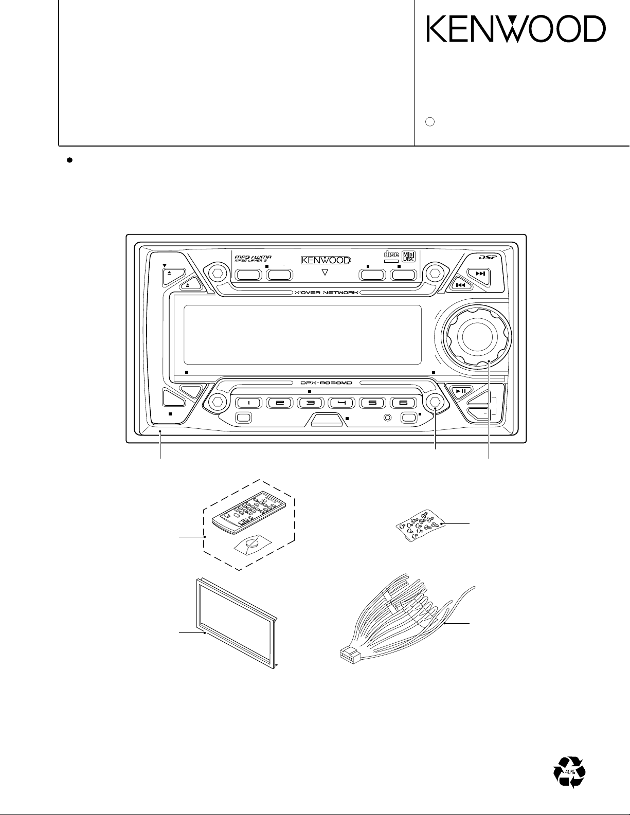
MD CD DSP RECEIVER
D PX -8030 MD
SERVICE MANUAL
2002-4 PRINTED IN JAPAN
C
B51-7924-00 (4) 517
This service manual dose not include information on the CD and MD mechanism assembly (exploded view, parts
list, schematic diagram and mechanism oparation description).
For such information, please refer to the CD mechanism assambly service manual (X92-4470-00 : B51-7899-00)
and MD mechanism assambly service manual (X92-4570-00 : B51-7887-00).
COMPACT
DIGITAL AUDIO
EJECT
CD
MD
MD CD DSP RECEIVER
DSP
AUD/ overX
EQ SEL S.A
Anti-Theft System Installed
FNC CLK
TEXT
50Wx4 MOS FET
MDLP
TUNE/SEEK
l
o
r
t
n
o
C
e
m
u
l
o
V
ANGLE
PANEL ASSY
(A64-2731-02)
REMOTE
CONTROLLER
ASSY
(A70-2028-05)
ESCUTCHEON
(B07-3025-02)
ANG
RTN
DISP
NAME
SCRL
SCN RDM G.RDM
SRC
REP
PWR OFF
System E's+
M.RDM
ATT
DEMO
CRSC
MACHINE SCREW
(N09-6027-05)
FM+
DISC
AM
KNOB (VOL.)
(K23-1064-03)
SCREW SET
(N99-1724-05)
DC CORD
(E30-4939-05)
2
DPX-8030 MD
ATT.
F/E
A8V
FM+B
AM+B
TUN5V
CLK
DATA
AUX
MD/CD CH
5L
IC4
A8V
MDS-3200W
BU5V,A8V
SRV+B
IC6
ANALOG
SW
A8V
ANALOG SW
DXM-6502W(J)
DXM-6500W(M)
SRV+B,SW5
BU5V,A8V
SW1-3
AMUTE
MRST
MSTOP
LO/EJ
MOTOR
DATA M
M CLK
LOS SW
M CLK
M DATA
A MUTE
M RST
M STOP
EJECT
LOAD
LOE SW
IC1
FSD
FMSD
IC2
A8V
E-VOL
MD DET
CD DET
FSD
LED OPEN
AUX : 455mV
CH : 1200mV
CD : 1200mV
MD : 1200mV
FM : 320mV
AM : 170mV
SYSTEM u-COM
BU5V
MD DET LED
CD DET
PON5V
X16
UNIT
FL
FL55V
FL3.3V ROM
FLFAC
INPUT
SEL
AM
FM
CH
ISO
TAPE
DSP DATAOUT
SP CLK SP INT CTS
SP DATA
SP REQ
KEY
MATRIX
RST SW
BU5V
BUFF
3.3V
DSP DATAIN
SC DATA RTS
MC DATA SC CON
X25 UNIT
E-VOL
DSP RST
DSP CLK
DSP SEL
PANEL
u-COM
BU5V
MUTE
FM : 603mV
AM : 428mV
CD : 1346mV
MD : 1346mV
CH : 1346mV
AUX : 511mV
IC15
RST
BU5V
IC7
LPF
MUTE
VREF
PMDET
PMOT1
PMOT2
PMODE
OPEN SW
IC14
P MECHA
M+,M-
IC4IC3
REMOCON
REMO+B BU5V
BU3.3V
IC8
DSP
DSPD3.3V
DSPA3.3V
REMO+B
3.3V
BU5V
VOL
IC5
SYSTEM
E’S
IC10
LPF BUFF
A8V
IC11
LPF BUFF
A8V
FM : 352mV
AM : 249mV
CD : 786mV
MD : 786mV
CH : 786mV
AUX : 298mV
FM : 1979mV
AM : 626mV
CD : 3512mV
MD : 3512mV
CH : 3512mV
AUX : 1494mV
DSPA3.3V
FM+B
AM+B
IC9
1/2VCC
FL55V
FLFAC
IC12
PWR IC
B. U.
MUTE
MUTE
AMP CTRL
SMALL DET
LINE MUTE BU DET
P CON
ANT CON
PON5V
DC/DC
PN M DR.
SW16V
MD SRV
SP OUT
FM : 1846mV
AM : 584mV
CD : 3277mV
MD : 3277mV
CH : 3277mV
AUX : 1394mV
B. U.
ACC DET
IC3
SW14V
A8V
DSP3.3V
BU5V
DC/DC+B
CD D+B
CD SRV
ILL+B
FRONT
PRE OUT
REAR/NF
PRE OUT
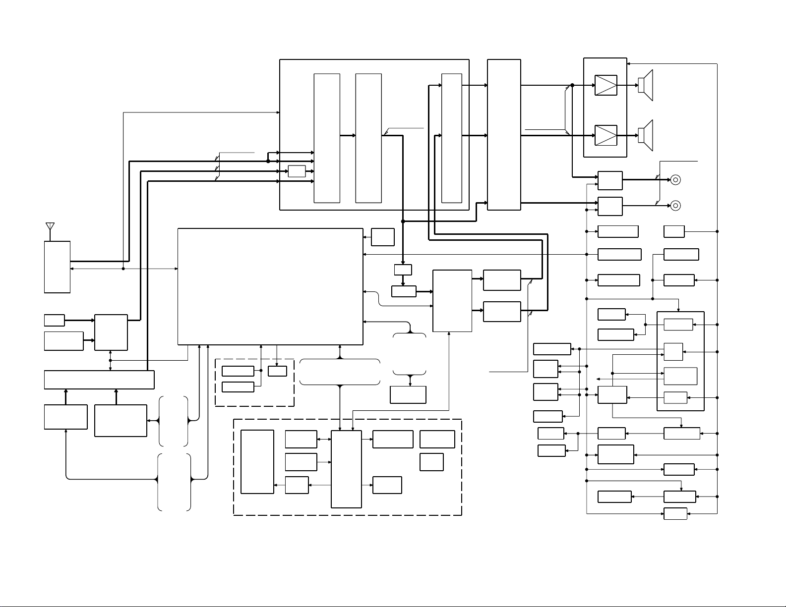
BLOCK DIAGRAM
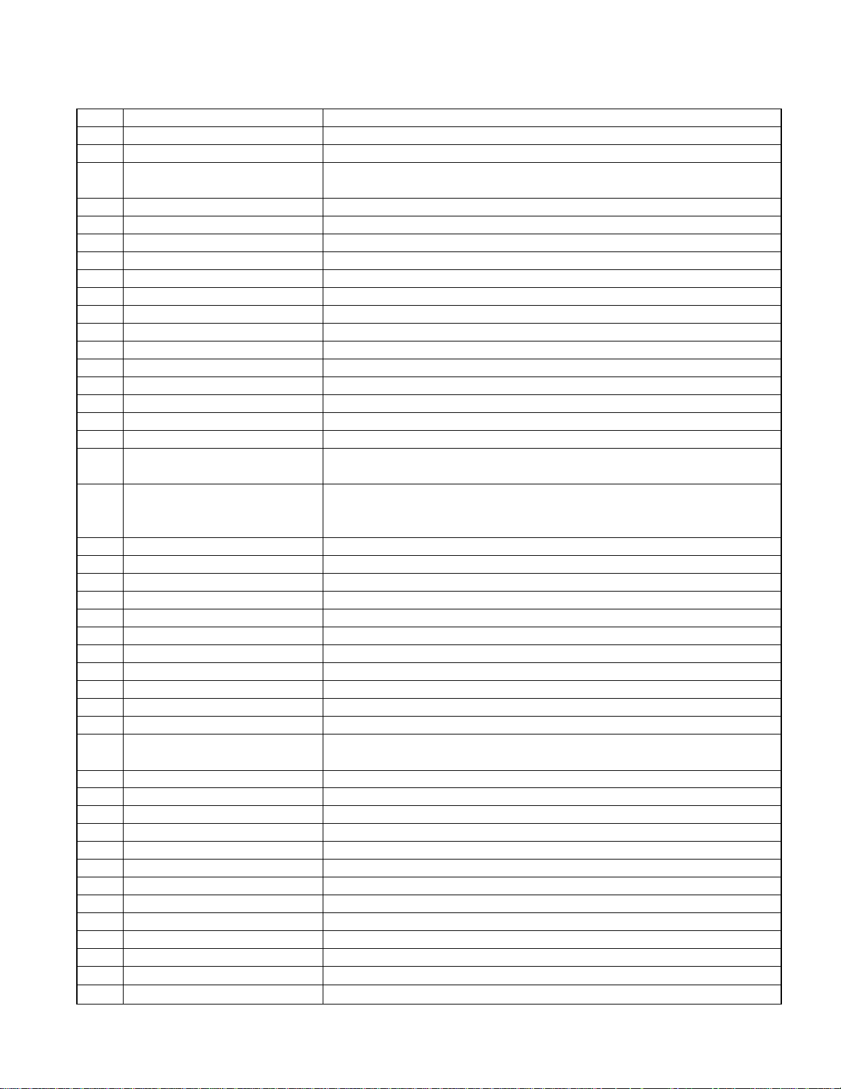
COMPONENTS DESCRIPTION
SYNTHESIZER UNIT (X14-6980-21)
•
Ref No.
IC1
IC2
IC3
IC4
IC5
IC6
IC7
IC8
IC9
IC10
IC11
IC12
IC13
IC14
IC15
IC16
IC17
Q1
Q2
Q3
Q5
Q6
Q7
Q8
Q9
Q10
Q11,12
Q13
Q14
Q15
Q16
Q17
Q18
Q19
Q20
Q21
Q22
Q23
Q24
Q25
Q26
Q52
Q53
Q54
Application/Function Operation/Condition/Compatibility
System µ-com
Input selector & electronic volume
Power supply IC
Analog switch
HPF and PRE-OUT (REAR NF)
Analog switch
LPF
DSP IC
4V AVR
LPF
LPF
POWER IC
5-pin regulator
Motor driver for panel mechanism
Reset IC
Logic IC
3-pin regulator
Surge detector switch
B.U/ACC detector switch
Dimmer switch
External amp control switch
P CON detector switch
P ANT switch
P ANT switch
P ON5V switch
CD servo supply 7.5V on/off switch
CD servo supply 7.5V AVR
CD servo supply 7.5V AVR
MD servo supply 5.0V AVR
MD servo supply 5.0V AVR
SW16V on/off switch
SW16V AVR
SW16V AVR
Illumination 11V on/off switch
Illumination 11V AVR
Illumination 11V AVR
FAC11V on/off switch
FAC1 1V AVR
FAC1 1V AVR
WMA DSP 5V ON/OFF SW
CD entrance LED on/off switch
AM +B SW
FM +B SW
FM/AM+B SW
DPX-8030 MD
Input source switching, SP=OUT/PRE-OUT electronic volume.
Generates BU 5V supply from B.UP,
and AUD 8V supply and DSP(D)3.3V supply and PCON output.
CD and MD input switching.
N/F electronic volume.
CD-CH and AUX input switching.
L,R output low-pass filter.
2-ch analog input, 4-ch analog output. (pos/neg phase PWM output)
LPF L,R channel reference supply.
Front L,R output low-pass filter.
Rear L,R output low-pass filter.
BTL Power amplifier.
WMA supply 5.0V, with variable output and on/off.
Output goes low on detecting voltage below 4.2 Volts.
Audio mute & power IC mute control.
DSP 3.3V supply.
Switch turns on when BU voltage surges to approx.
18.2 to 18.9 volts or more, and turns off BU detector switch.
Base goes Hi, when BU voltage is applied and turns on. When an instantaneous
voltage drop is detected and BU turns off or when shutoff, the base goes Lo and
turns off. Base goes Hi, and transistor turns on when Acc voltage is applied.
Base goes Hi, and transistor turns on when vehicle lights turn on.
Turns on when base goes Lo and outputs control signal.
Base goes Hi, and transistor turns on when P CON is output.
When base of Q8 goes Hi, Q7 turns on and P ANT output.
Turns on when base goes Hi, and applies voltage to PON 5V line.
Turns on when base goes Hi, and turns on CD servo 7.5 volt supply.
When base of Q13 goes Hi, AVR output turns on.
When base of Q15 goes Hi, AVR output turns on.
Turns SW16V AVR on and off. Turns on when base goes Hi,
and turns on the SW16V output.
SW16V output turns on when Q18 base goes HI.
Turns on when base goes Hi, and turns on the 11 volt LED supply.
Turns on when base of Q21 goes Hi and turns on the 11V output.
Turns on when base goes Hi, and turns on FAC11V.
Turns on when base of Q24 goes Hi, and turns on FAC11V output.
Turns on when base goes Hi, and turns on the WMA DSP 5 volt supply.
Turns on when base goes Hi, and turns on LED of CD entrance.
During AM operation, base goes Lo and turns on.
During FM operation, base goes Lo and turns on.
During FM/AM operation, base goes Hi, and Q52 or Q53 turn on and off.
3

DPX-8030 MD
COMPONENTS DESCRIPTION
Ref No.
Q101
Q102
Q201
Q202
Q301
Q302
Q401
Q402
Q403,404
Q405
Q406,407
Q801
SWITCH UNIT (X25-9320-00)
•
Ref No.
IC1
IC2
IC3
IC4
IC5
Q1
Q2
Q3
Q4
Q5
Q6
Q7
Application/Function Operation/Condition/Compatibility
RST DRIVER
RST SW
Audio mute SW
Audio mute SW
Audio mute SW
Audio mute SW
MD/CD analog selector switch
CD-CH/AUX analog selector switch
Electronic volume mute switch
PWIC mute switch
Mute driver
Panel mechanism voltage selector
Application/Function Operation/Condition/Compatibility
Logic IC (buffer)
Power supply IC
Panel µ-com
Remote control IC
Memory IC
Panel µ-com reset switch
PON 5 volt supply switch
PON control switch
FL+B (50V) supply switch
FL+B (50V) control switch
VFD BD section blanking switch
DSI control switch
Turns on when base goes Lo and sends a reset signal to the system
µ-com/panel µ-com/changer.
Turns on when base goes Hi and resets the system µ-com.
Front L-ch mute, turns on when base goes Hi.
Rear/nonfader L-ch mute, turns on when base goes Hi.
Front R-ch mute, turns on when base goes Hi.
Rear/nonfader R-ch mute, turns on when base goes Hi.
Turns on when base goes Hi, controls IC4 output.
Turns on when base goes Hi, controls IC6 output.
Turns on when base goes Lo, sends mute signal to electronic volume mute
SW.
Turns on when base goes Hi.
Turns on when base goes Lo, sends mute signal to audio mute SW.
Turns on when base goes Hi, lowers the panel motor drive voltage.
Control signal voltage convertor for VFD, BD sections. (5V 3.3V)
3.3V AVR. (VDD1B 5V 3.3V)
Remote control signal receiver & control signal output.
Turns on when base goes Hi and resets the Panel µ-com.
Turns on when base goes Lo and turns on PON5V.
Turns on when base goes Hi and turns on Q10.
Turn on when base goes Lo, and turns on FL+B.
Turn on when base goes Hi, and turns on Q3.
Turns off when base goes Lo, and turn on a light BD section.
Turns on when base goes Hi, and turn on the DSI LED.
SUB-CIRCUIT UNIT (X16-1710-00)
•
Ref No.
PH1
PH3
Application/Function Operation/Condition/Compatibility
CD disc sensor
MD disc sensor
4
When sensor detects infrared light, optical current proportional to that current
flows in collector.
When sensor detects infrared light, optical current proportional to that current
flows in collector.

MICROCOMPUTER'S TERMINAL DESCRIPTION
(X14-) IC1 : System µ-com
PIN No.
1
2
3
4
5
6
7
8
9
10
11
12
13
14
15
16
17
18
19
20
21
22
23
24
25
26
27
28
29
30
31
32
33
34
35
36
37
38
39
40
41
42
43
44
DSP RVDT
DSP CLK
DSP RST
DSP XLAT
CH DATAH
CH DATAC
CH CLK
BYTE
CNVss
CH CON
CH REQH
RESET
Xout
Vss
Xin
Vcc
NMI
PN REQ
SP INT
CH REQC
BU DET
ACC DET
ILLUMI
AMP CTRL
TEST
BUZZ
PWIC SVR
PWIC STBY
SCL
SDA
SYS-DATA
PN-DATA
PN CLK
SYS REQ
TEL DAOUT
TEL DAIN
PANT
PCON IN
PCON
PON
LAMP
LED OPEN
SI
NC
I/OPin Name Description Processing Operation
O
O
O
O
O
I
I/O
I
I
O
O
I
O
I
I
I
I
I
I
I
I
I
I
O
O
O
O
O
I/O
I/O
O
I
O
O
O
I/O
O
I
O
O
O
O
O
O
DSP data output terminal
DSP clock output terminal
DSP reset terminal
Address data selector terminal
External CH data output terminal
External CH data input terminal
External CH clock I/O terminal
External data bus pulse width switcher
Processor mode switcher
External CH selector terminal
External CH transmit request terminal
Reset input
µ-com operating frequency (out)
µ-com GND
µ-com operating frequency (in)
Positive power supply terminal
NMI (non-maskable interrupt) terminal
Panel communications line
Spectrum analyzer request
External CH receive request terminal
Instantaneous port voltage detector terminal
ACC detector terminal
Illumination detector terminal
External amp control
Power IC control terminal
Beep output
Power IC control terminal
Power IC standby terminal
I2C clock output terminal
I2C data I/O terminal
Panel communications data OUT terminal (Flash TxD)
Panel communications data IN terminal (Flash RxD)
Panel communications CLOCK (Flash SCLK)
Panel communications control line (Flash BUSY)
Hands-free data OUT terminal
Hands-free data IN terminal
Power antenna terminal
External amp overcurrent terminal
External amp current control terminal
Power control terminal
Lamp control terminal (Flash EPM)
LED control terminal for CD, MD
LED control terminal
OPEN
DPX-8030 MD
500kHz
L reset, Low pulse width : 450ms
N5L: System controller output,
O5L: Input,Input when not connected
During normal operation: L,
During flash writing: H
L when not connected,
H: during CH1 for O5L, Others: L
Normally at H after N5L is recognized.
L during system controller output
L: Reset, reset voltage 4.2 volts
L: Normally on H: Instantaneous port voltage
H:ACC OFF
L: Small ON
L: Test mode H: Non test mode
H:ON
500kHz
H: Use L: LOW fixed
H: Use L: Input
H: ANT ON L: ANT OFF
H: Triggers protection circuit L: In normal operation
Logic level when ON: H
During ALL OFF is L (during TEL: H)
H:ON
H: ON (Illumi triggered)
EPM terminal for flash writing
ON if opened other than at CD Eject position
H: Lights up
Fixed at LOW
5

DPX-8030 MD
MICROCOMPUTER'S TERMINAL DESCRIPTION
PIN No.
45
46
47
48
49
50
51
52
53
54
55
56
57
58
59
60
61
62
63
64
65
66
67
68
69
70
71
72
73
74
75
76
77
78
79
80
81
82
83
84
85
86
87
88
89
90
91
92
SP REQ
PN SCCON
SEL E2PROM
CD PON
PMOT1
PMOT2
PM VR
PMDET
OPEN SW
CD MOTOR
CD LO/EJ
CD LOE/LIM SW
CD 8EJE SW
CD MSTOP
CD AMUTEL
CD LOS SW
CD 12EJE SW
CD AMUTER
MD LOS/EJE SW
MD AMUTE
MRST
MD MSTOP
MD EJECT
MD LOAD
MD LOE/LIM SW
TEL C
TEL MUTE
V DOWN
V RST
PLUG SW
TYPE AUX
CRSC SEL1
CRSC SEL2
NC
TYPE TEL
TYPE DIVER
MUTE
PW MUTE
ASEL 1
ASEL 2
FM+B
AM+B
SD
DIVER
FSD OUT
REFCON
I/OPin Name Description Processing Operation
O
Spectrum analyzer enable output
O
Panel communications line (Flash CE)
I
E2PROM inserted/not inserted
O
CD WMA power supply control terminal
O
Panel motor control terminal
O
Panel motor control terminal
O
Panel mechanism voltage control terminal
I
Panel mechanism detect terminal
I
Panel full-open detect terminal
O
CD motor control terminal
I/O
CD motor control terminal
I
CD mechanism SW3 detect terminal (Clamping SW)
I
CD mechanism detect terminal
O
CD mechanism control stop terminal
I
CD mute request terminal
I
CD loading detect terminal
I
CD mechanism detect terminal (8cm/12cmSW)
-
µ-com power supply
I
CD Mute request terminal
-
µ-com GND
I
MD disc position detect output (load start switch)
I
MD MUTE request terminal
O
CD/MD µ-com RST terminal
O
MD mechanism control stop terminal
O
MD motor control terminal
O
MD motor control terminal
I
MD mechanical detect terminal (clamping switch)
O
Cell phone connection control terminal
O
Cell phone mute terminal
O
Mute terminal to Hands-free DSP IC
O
Resets the Hands-free DSP IC
O
Easy hands-free selector terminal
I
AUX yes/no setting
I
Destination setting
I
Destination setting
O
Not used
I
Cell phone yes/no setting
I
DIVER yes/no setting
O
Mute terminal
O
Power IC mute control terminal
O
INPUT selector terminal 1
O
INPUT selector terminal 2
O
FM power terminal
O
AM power terminal
I
Broadcast station detection terminal
O
FM DIVER selector switch
I
S meter input terminal
O
A/D reference voltage output
Active at L
Writes at H
L: ON
H: Low torque L: Normal torque
L: Panel mechanism H: No panel mechanism
L: Panel full-open
L: DISC in switch position
L: DISC in switch position
H: Now at CD source
L: DISC in switch position
L: 12cm H:8cm
H: DISC inserted (during loading)
L: Eject finish position (during eject)
L: Mute ON (MD source only)
L: RESET
H: MD mechanical startup
L: No MDPACK H: MDPACK
L: Private or POWER OFF
H: TEL MUTE ON
L: MUTE ON
L: RESET
PULG:H Bus:L
H: AUX function present
OPEN
H: Yes L: No
H: DIVER function present
H: MUTE ON
L: MUTE ON
L: During ALL OFF & Instantaneous port voltage
L: CD H:MD
L: CH H:AUX
H: FM (however is Lo at AM+B: L)
H: AM (however is Lo at FM+B: L)
H: Station found
L: DIVER ON H: DIVER OFF or during AM
H: Station found (A/D input), Vth is by F/E setting
6

DPX-8030 MD
MICROCOMPUTER'S TERMINAL DESCRIPTION
PIN No.
PMODE
93
CD DET
94
MD DET
95
Avss
96
LINE MUTE
97
Vref
98
Avcc
99
NC
100
(X25-) IC3 : Panel µ-com
PIN No.
1
GS01
2
GCLK
3
NC
4
REMO
5
GS02
6
NC
7
GCLK
8-11
NC
12
GCP
13
NC
14
GBK
15
BYTE
16
CNVss
17
NC
18
NC
19
RESET
20
Xout
21
Vss
22
Xin
23
Vcc
24
NC(NMI)
25
SP REQ
26
SYS REQ
27
PN SC CON
28,29
NC
30
SCL
31
SDA
32
GLAT
33
SP INT
34
NC
35
DSP CLK
36
SP DATA IN
37
NC
38
PN DATA
39
Vcc
40
SYS DATA
41
Vss
42
PN CLK
43
PN REQ
I/OPin Name Description Processing Operation
I
Panel position sensor input terminal
I
CD photosensor terminal
I
MD detector terminal
I
AD converter ground potential
I
LINE MUTE ON/OFF detector terminal
-
AD converter reference voltage
I
AD converter positive power supply voltage
I
Not used
I/OPin Name Description Processing Operation
O
FL dot section data output terminal 1
O
FL dot section clock output terminal
O
Not used
I
Remote control signal input
O
FL dot section data output terminal 2
I
Not used
I
FL dot section clock input terminal
O
Not used
O
FL dot section gradation generation
O
Not used
O
FL dot section data blanking output
I
GND potential
I
GND
I
Not used
O
Not used
I
µ-com Reset
O
µ-com operating frequency (out)
I
GND potential
I
µ-com operating frequency (in)
I
Positive power supply terminal
I
Connect to 5 volt potential
I
Spectrum analyzer enable input
I
System controller communication request input
I
System controller communication panel operation
O
Not used
I/O
E2PROM writing clock terminal
I/O
E2PROM writing terminal
O
FL dot data latch output
O
Spectrum analyzer data request
O
Not used
I
Spectrum analyzer data input clock
I
Spectrum analyzer data input
O
Not used
O
System control communication data output
I
Positive power supply terminal
I
System control communication data input
I
GND potential
I
System controller communication clock input terminal
O
Panel communication request output
(A/D input) Vth is set in test mode
L: CD present (A/D input) Vth: 2.2 volts
L: MD present (A/D input) Vth: 2.8 volts
OFF at 1.0 - 2.5 volts, ON at all other voltages
Connect to GND potential
3.3MHz
L: Fixed
Connect to GND potential
L: Fixed
L: Fixed
H: Turn on a light L: Off
W3: L due to 16 bit pulse width
L: Fixed
L: Reset
L: Operation OK
L: Fixed
P-OFF: Output L, P-ON: Output L/input
P-OFF: Output L, P-ON: Output L/input
L: Fixed
L: Fixed
7

DPX-8030 MD
MICROCOMPUTER'S TERMINAL DESCRIPTION
PIN No.
44
45
46
47
48
49-51
52
53
54
55,56
57
58
59
60-62
63
64
65
66-69
70
71
72
73
74
75
76
77
78
79
80
81
82
83
84
85
86-90
91
92
93
94
95
96
97
98
99
100
101
102
103
104
105
GS03
NC
FL CLK
NC
SEL E2P
NC
RDY
NC
HOLD
NC
Vss
NC
Vcc
NC
RD
NC
WR
NC
CS0
A21
A20
A19
Vcc
A18
Vss
A17
A16
A15
A14
A13
A12
A11
A10
A9
NC
Vcc
A8
Vss
A7
A6
A5
A4
A3
A2
A1
A0
D15
D14
D13
D12
I/OPin Name Description Processing Operation
O
FL dot section data output terminal 3
O
Not used
I
FL dot section clock input terminal
O
Not used
I
E2PROM writing request
O
Not used
I
RDY request
O
Not used
I
5 volt potential
O
Not used
I
GND potential
I
Not used
I
Positive power supply terminal
O
Not used
O
External memory read request
O
Not used
O
External memory write request
O
Not used
O
F/MEMORY CE terminal
O
External bus ADDR 21
O
External bus ADDR 20
O
External bus ADDR 19
I
Positive power supply terminal
O
External bus ADDR 18
I
GND potential
O
External bus ADDR 17
O
External bus ADDR 16
O
External bus ADDR 15
O
External bus ADDR 14
O
External bus ADDR 13
O
External bus ADDR 12
O
External bus ADDR 11
O
External bus ADDR 10
O
External bus ADDR 9
O
Not used
I
Positive power supply terminal
O
External bus ADDR 8
I
GND potential
O
External bus ADDR 7
O
External bus ADDR 6
O
External bus ADDR 5
O
External bus ADDR 4
O
External bus ADDR 3
O
External bus ADDR 2
O
External bus ADDR 1
O
External bus ADDR 0
I
External bus DATA 15
I
External bus DATA 14
I
External bus DATA 13
I
External bus DATA12
L: Fixed
L: Fixed
H: Write
L: Fixed
L: Fixed
L: Fixed
L: Fixed
L: Fixed
L: Read
L: Fixed
L: Write
L: Fixed
L: Select external ROM
L: Fixed
16-bit pulse width is OPEN
8

DPX-8030 MD
MICROCOMPUTER'S TERMINAL DESCRIPTION
PIN No.
106
107
108
109
110
111
112
113
114-118
119
120
121
122
123
124
125
126
127
128
129
130
131
132
133
134
135
136
137
138
139
140
141
142
143
144
D11
D10
D9
D8
D7
D6
D5
D4
NC
D3
D2
D1
D0
NC
RE IN
RE BASE
KS0
KS1
KS2
KS3
Vss
KS4
Vcc
NC
DC/DC SW
PN PON
KR0
KR1
KR2
KR3
Avss
KR4
Vref
Avcc
NC
I/OPin Name Description Processing Operation
I
External bus DATA 11
I
External bus DATA 10
I
External bus DATA 9
I
External bus DATA 8
I
External bus DATA 7
I
External bus DATA 6
I
External bus DATA 5
I
External bus DATA 4
O
Not used
I
External bus DATA 3
External bus DATA 2
I
External bus DATA 1
I
External bus DATA 0
I
Not used
O
B input
I
A input
I
Key-scan output 0
O
Key-scan output 1
O
Key-scan output 2
O
Key-scan output 3
O
GND potential
I
Key-scan output 4
O
Positive power supply terminal
I
Not used
O
DC/DC FL terminal selector terminal
O
Power control terminal
O
Key-return signal input 0
I
Key-return signal input 1
I
Key-return signal input 2
I
Key-return signal input 3
I
GND potential for AD converter
I
Key-return signal input 4
I
AD converter reference voltage
I
AD converter positive power supply
I
Not used
I
L: Fixed
L: Fixed
L: Fixed
Dependent on PN PON
Connect to GND potential
Connect to GND potential
9
 Loading...