

Kenwood DMS-E7, DMS-E9, DMSE-7-G Service manual
MINIDISC RECORDER
8
4
1
¢
¡
7
0
3
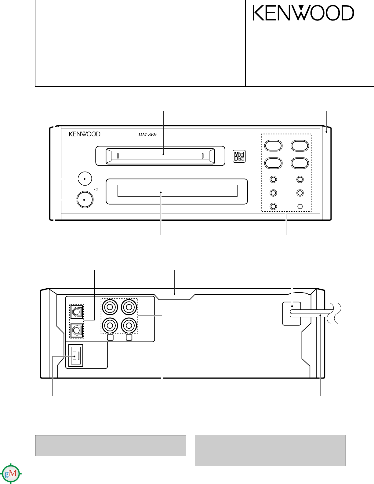
minidisc recorder
rec
level
O.T.E.
on/standby
D.R.I.V.E.
LR
DIGITAL IN
OPTICAL
SYSTEM
CONTROL
REC
IN
PLAY
OUT
1
2
DM-SE7/SE7(G)/SE9
SERVICE MANUAL
© 1997-11/B51-5395-00 (K/K) 3191
Indicator
(B12-0318-04)
Knob*
(K29-)
Optic receiving module
(W02-1181-05)
Escutcheon*
(B07-)
Front glass
(B10-2372-03)
Metallic cabinet*
(A01-)
Panel*
(A60-)
Knob*
(K29-)
Power cord bushing
(J42-0083-05)
Phono jack
(E63-0120-05)
Rectangutar receptacle
(E08-0311-05)
In compliance with Federal Regulations, following are reproductions of labels on, or inside the product relating to laser product
safety.
KENWOOD-Crop. certifies this equipment conforms to DHHS
Regulations No. 21 DFR 1040. 10, Chapter 1, Subchapter J.
DANGER : Laser radiation when open and interlock defeated.
AVOID DIRECT EXPOSURE TO BEAM
* Refer to parts list on page 21.
Illustration is DM-SE9.
AC power cord*
(E30-)
Beware of condensation
When water vapor comes into contact with the surface of
cold material, water drops are produced. If condensation
occurs, correct operation may not be possible, or the unit
may not function correctly.
This is not a malfunction, however, and the unit should be
dried.
(To do this, turn the POWER switch ON and leave the unit
as it is for several hours.)
Be especially careful in the following conditions:
• When the unit is brought from a cold place to a warm place
and there is a large temperature difference.
• When a heater starts operating.
• When the unit is brought from an air-conditioned place to
a place of high temperature with high humidity.
• When there is a large difference between the internal
temperature of the unit and the ambient temperature, or in
conditions where condensation occurs easily.
DM-SE7/SE7(G)/SE9
N O DIS
C
CONTENTS / ACCESSORIES / CAUTIONS
Contents
CONTENTS / ACCESSORIES / CAUTIONS...............2
CIRCUIT DESCRIPTION.............................................3
PC BOARD ................................................................. 6
SCHEMATIC DIAGRAM............................................. 9
Accessories
EXPLODED VIEW .....................................................19
PARTS LIST...............................................................21
PARTS DESCRIPTIONS...........................................27
SPECIFICATIONS .......................................Back cover
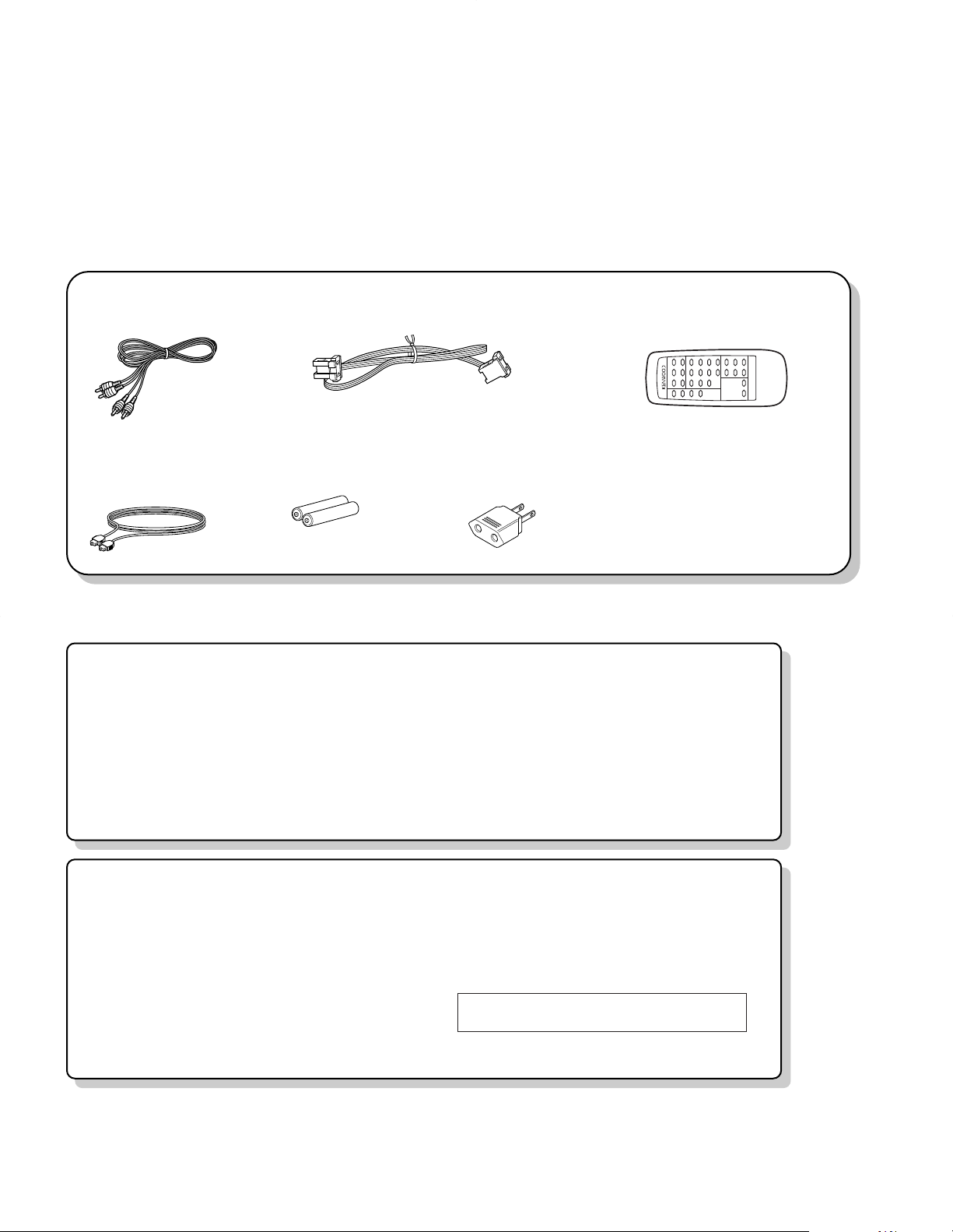
Audio cord
(E30-0615-05)
Optical fiber
(B19-1529-05)
Cautions
System control cord
(E30-2628-05)
Batteries (2)
Remote control unit
(A70-1153-05) : RC-MSE7
(A70-1169-05) : RC-MSE9
Battery cover (A09-0129-08 : RC-MSE9)
(A09-0356-08 : RC-MSE7)
AC plug adapter
(E03-0115-05)
Note related to transprotaion and movement
Before transporting or moving this unit, carry out
the following operations.
1. With no disc loaded in the unit, press the "on /
standby" key to on.
• Check that no disc is present in the unit.
2. Wait a few seconds and verify that the display
shown appears.
3. Press the "on / standby" key to off (standby).
2
CIRCUIT DESCRIPTION
PROTECT 23
REFLECT 20
DISCIN 25
STTLMT 24
PHOTSW 21
RECSW 19
LOADIN 32
LOADOUT 31
DRDT 73
DEMPH 77
DDQSY 48
DLAT 76
DSUB1 80
DSUB2 79
DWDT 74
DCLK 75
FLDCE 3
SRCLAT 78
VLCK 26
VLDT 63
VOLLAT 71
SBUSY 81
SDATA 82
KR1 54
KR2 55
KR3 56
INISW 58
1 A16
2 A17
84 AD0
: :
91 AD7
92 A8
: :
99 A15
5 RD
6 WR
7 CS
8 ASTB
33 SCHNG
13 SCL
34 SDA
28 XLAT
15 SENS
30 MNT0
14 MNT2
12 XRST
35 TX
27 RECP
29 MNT3
45 XINT
47 SQSY
48 DQSY
50 MNT1
65 SRDT
66 SWDT
67 SCLK
16 POWER
72 MUTE
17 LDON
18 RMS
36 BACKCHK
44 REM
46 CE
59 BACKV
83 BACKON
uPD784215GF506
E2PROM
CXD2652AR
MDM-04
LC8904Q
LC75710NE
SM5844AF
EXDT10EXLAT11EXCK
4
Q1
Q2 FLRST
Q3 ADRST
Q4 DIGRS
DRIVE Q5
DINSEL Q6
EMPHA Q7
DARST Q8
RAM
(X25)IC21
(X33)IC6
(X33)IC2
(X25)IC11
(X14)IC1
(X25)IC13
(X25)IC2
(X25)J3
(X25)IC15
MECHA
ELECTRIC Vol.
SERIAL.
1. Main microprocessor : uPD784215GF506
1-1 Microprocessor periphery block diagram
DM-SE7/SE7(G)/SE9
3
DM-SE7/SE7(G)/SE9
CIRCUIT DESCRIPTION
1-2 Pin description
No. Name I/O Description
1,2 A16,17 O SRAM address
3 FLDCE O FL display driver CE
4 EXCK O Extension port clock
5 RD O SRAM reading
6 WR O SRAM writing
7 CS O SRAM CS (L:SRAM enable)
8 STB O SRAMASTB
9 Vdd - Microcomputer power supply
10 EXDT O Extension port data
11 EXLAT O Extension port latch
12 XRST I System IC reset
13 SLC O E2PROM clock
14 MNT2 I System IC BUSY
15 SENS I System IC SENS
16 POWER O POWER (H:Power on)
17 LDON O Laser ON (H:Laser diode ON)
18 RMS O Pickup microwave satisfactory (H:ON)
19 RECSW I Mechanism REC position switch (L:REC SW ON)
20 REFLECT I Disc high reflex / low reflex switch (L:High reflex)
21 PHOTSW - Mechanism PLAY position detection
(L:Phot sensor ON)
22 (GND)TEST - Microcomputer power supply
23 PROTECT I Disc protect switch
24 STTLMT I Mechanism pickup position switch
(L:Start limit SW ON)
25 D1SCIN I Mechanism disc insertion switch (L:Disc out SW ON)
26 VLCK O SRC clock
27 RECP O System IC RECP
28 XLAT O System IC latch
29 MNT3 I System IC spindle LOCK
30 MNT0 I System IC FOK
31 LOADOUT O Loading motor OUT direction drive (L:Loading IN)
32 LOADIN O Loading motor IN direction drive (L:Loading OUT)
33 SCHNG O E2PROM data output change (H:SDA output)
34 SDA I/O E2PROM data
35 TX O System IC TX
36 BACKCHK O Back-up voltage check ON
37 Vdd - Microcomputer power supply
38 X2 O Oscillation element (12.5MHz)
39 X1 I Oscillation element (12.5MHz)
40 VSS - Microcomputer power supply
41,42 XT2,1 O Clock oscillation element (Unused)
43 RESET I Microcomputer reset
44 REM I Remote control input
45 XlNT I ATRAC interrupt
46 CE I Microcomputer CE
47 SQSY I SYNC interrupt
48 DQSY I Inner DlN interrupt
49 SSQSY I External DlR interrupt
50 MNT1 I System IC shock detection
51 Vdd - Microcomputer power
52 +5V - A/D standard voltage
No. Name I/O Description
53 - I Unused
54~56 KR1~3 I Key return 1~3
57 - I Unused
58 INISW I Destination change
59 BACKV I Backup voltage detection
60 - I Unused
61 GND - Microcomputer power
62 - I Unused
63 VLDT O SRC data
64 +5V - D/A standard voltage
65 SRDT I System IC input data
66 SWDT O System IC output data
67 SCLK O System IC clock
68 CRXD I External unit receiving data
69 CTXD O External unit transmission data
70 CENA I External unit correspondence permission
71 VOLLAT O Electron volume latch
72 MUTE O MUTE terminal
73 DRDT I DIR reading data
74 DWDT O DIR, display driver data
75 DCLK O DIR / display driver clock
76 DLAT O DIR latch
77 DEMPH I DIR emphasis
78 SRCLAT O SRC latch
79,80 DSUB2,1 I DIRSUB2,1
81 SBUSY O 16bit synchro BUSY
82 VLCK O 16bit synchro DATA
83 BACKON O Back-up voltage charge ON
84-91 AD0~7 O SRAM address / data
92-99 A8~15 O SRAM address / data
100 Vss - Microcomputer power
4
DM-SE7/SE7(G)/SE9
CIRCUIT DESCRIPTION
1-3 Backup
Each following condition is backup to the memory with
ON/OFF of the AC power.
• Information of TOC
• UTOC information
(Settlement contents of “editing etc. of record, TRACK editing, titles”)
• Condition of POWER ON/OFF
• Condition of REC INPUT
• Condition of AUTO/MANUAL
• Setting of DIGITAL REC LEVEL
• Contents of the presetting title
1-4 Initial state
POWER =OFF
REC INPUT =ANALOG
AUTO MANUAL =AUTO
PLAY MODE =TRACK
REPEAT =OFF
TIME DISPLAY =SINGLE(+)
REC LEVEL =-12dB
DRIVE =ON
Preset title =PRE1 : Pops
=PRE2 : Rock
=PRE3 : Classic
=PRE4 : Jazz
=PRE5 : Disco
=PRE6 : Best Hits
=PRE7 : Air Check
=PRE8 : No.
=PRE9 : Vol.
1-5 Way of resetting a microprocessor
When turning on while pressing EJECT key,
DM-SE7/SE9 initializes and starts a microprocessor.
INI SW 58pin Description
High Overseas; KATAKANA uncorrespondence.
CYBER TITLER uncorrespondence.
Low Japan ; KATAKANA correspondence.
CYBER TITLER correspondence.
1-6 Key matrix :
0.00 0.49 1.48 2.48 3.48 KEY OFF
-0.47V -1.46V -2.46V -3.46V -4.45V 4.47-5.0V
KR 0 - - - - - -
÷÷ 88
KR 1
33 77 ¡¡ 11
KR 2
KR 3 -
*DM-SE7/SE9 doesn’t function.
Mode for the inspection : It utilizes for the existence or non-
existence of the FL display.
• Way of setting
Turn on the AC power while pressing STOP(7)key.
• Way of canceling
Press STOP(7)key.
• Contents
Press(¢)key or(4) key.
Then, DM-SE9 becomes the following test mode.
Press PLAY(3) key, to fix each test mode.
To cancel each test mode, Press PLAY(3) key once again.
*O.T.E *ATT UP *ATT -
DOWN
REC INPUT
00 ¢¢ 44
DISPLAY
TIME
• SEG TEST
(When PLAY key is pressed all FL are lighted.
Indication changes cyclically as follows when ¢ or 4
key are pressed.)
“All FL light up”
“FL turn off the lights”
“KATAKANA”
“All FL light up”
• KEY TEST
(For the mode for the production line, in the service, it doesn’t use.)
1-7 Extension IC
PIN No. IC Port name I/O Explanation
4 Q1 - O DIN selector 1
5 Q2 FLDRST O FL driver reset
6 Q3 ADRST O A/D reset
7 Q4 DIGRST O DIN reset
14 Q5 DRIVE O Drive ON/OFF
13 Q6 DINSEL2 O DIN selector 2
12 Q7 EMPHA O Play emphasis ONÅ^OFF
11 Q8 DARST O D/A reset
2. Adjustment
Refer to the adjustment ( the page ) of the service manual
(B51-5387-00) of 1050MD/DM-5090/9090.
But, the key to operate is different as follows.
DM-SE7/SE9 1050MD/DM-5090/9090 Description
PLAY ENTER Decision of MODE
STOP FADE / DELEAT Cancellation of MODE
PAUSE SET Go to the next step
DM-SE7/SE9 1050MD/DM-5090/9090 Description
A continuation replay /
STOP FADE / DELEAT continuation recording
are canceled.
The thread moves to the
FF FF periphery only while
pressing a key.
The thread moves to the
FB FB internal circumference
only while pressing a key.
The continuation
recording menu choice
Every time pressing a
- REC INPUT key, DM changes the
mode at the pit and the
groove "
- REC MODE Spindle servo mode
change (CLVS and A)
Every time pressing a
O.T.E TITLE INPUT key, DM changes the
contents of the display.
• DOT TEST
(It becomes “Niagara indication” when PLAY key is
pressed.)
5
A
CB D
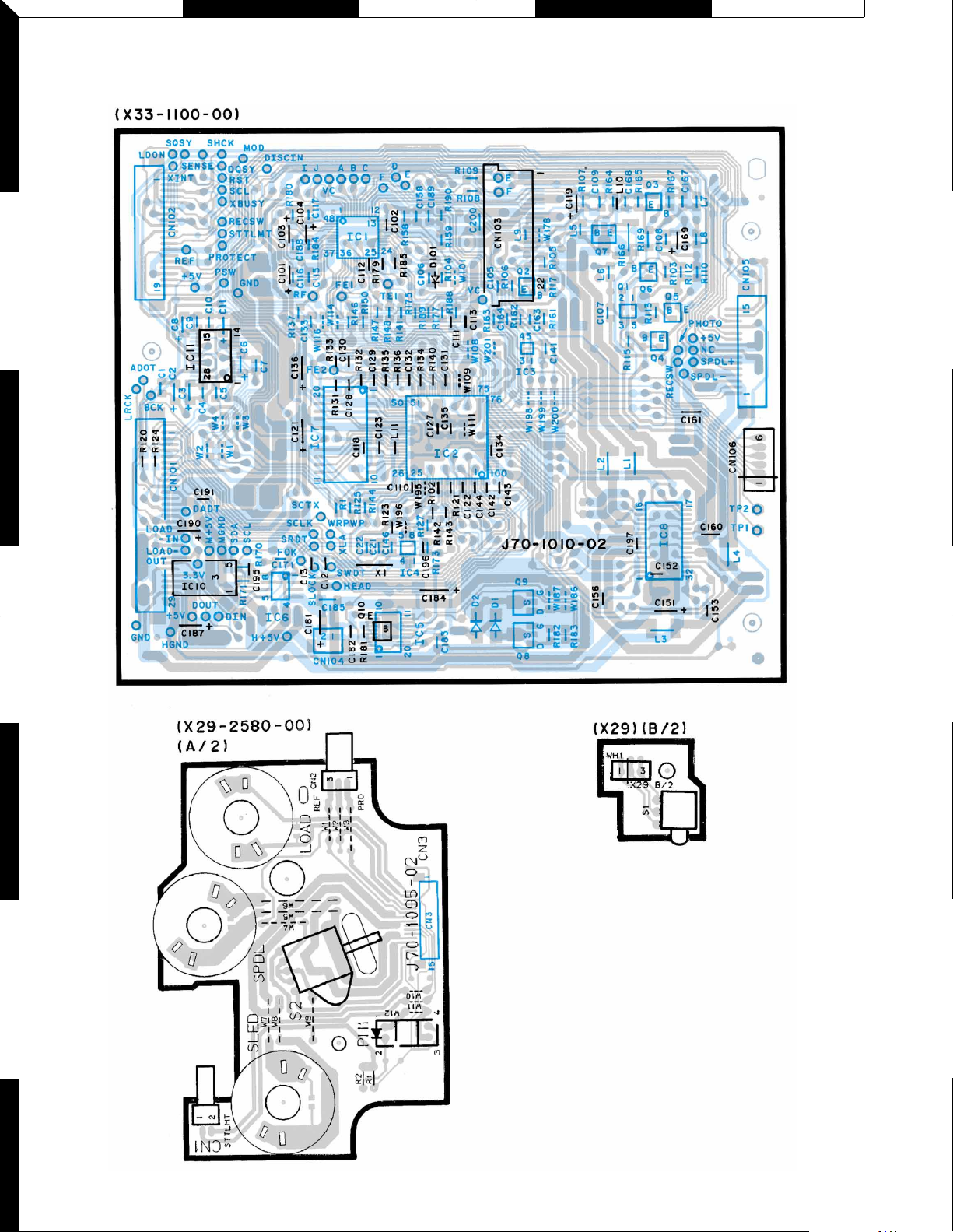
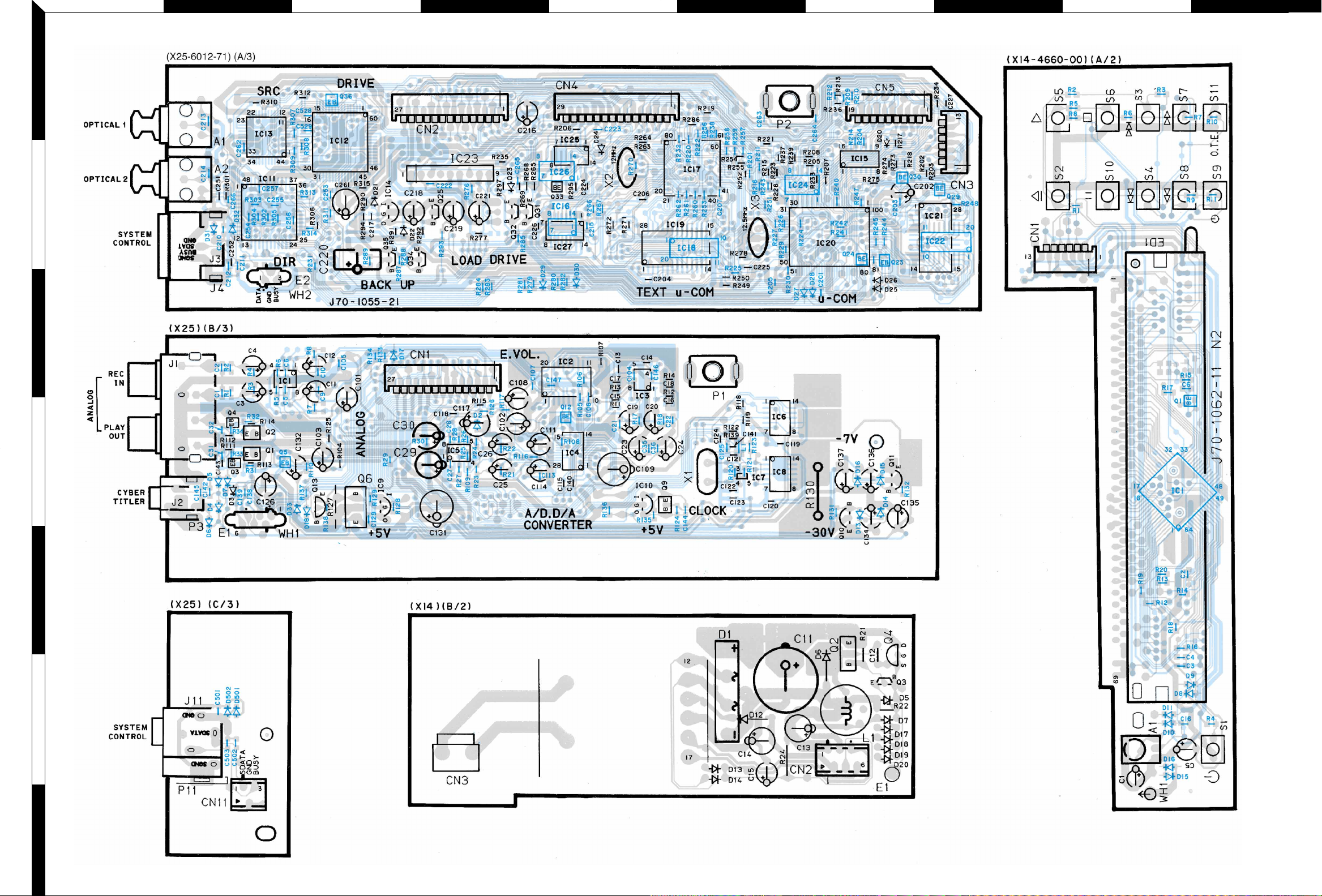
PC BOARD(Component side view)
E
1
2
3
MD MECHANISM UNIT
4
MD CONTROL UNIT
5
6
7
6
Refer to the schematic diagram for the value of resistors and capacitors.
FHJLNGIKMO
PC BOARD(Component side view
1
2
3
)
4
5
6
7
Refer to the schematic diagram for the value of resistors and capacitors.
7 8
 Loading...