

Page 1

Model 224 Programmable Current Source
Instruction Manual
A GREATER MEASURE OF CONFIDENCE
Page 2

WARRANTY
Keithley Instruments, Inc. warrants this product to be free from defects in material and workmanship for a period of 1 year
from date of shipment.
Keithley Instruments, Inc. warrants the following items for 90 days from the date of shipment: probes, cables, rechargeable
batteries, diskettes, and documentation.
During the warranty period, we will, at our option, either repair or replace any product that proves to be defective.
To exercise this warranty, write or call your local Keithley representative, or contact Keithley headquarters in Cleveland, Ohio.
You will be given prompt assistance and return instructions. Send the product, transportation prepaid, to the indicated service
facility. Repairs will be made and the product returned, transportation prepaid. Repaired or replaced products are warranted for
the balance of the original warranty period, or at least 90 days.
LIMITATION OF WARRANTY
This warranty does not apply to defects resulting from product modification without Keithley’s express written consent, or
misuse of any product or part. This warranty also does not apply to fuses, software, non-rechargeable batteries, damage from
battery leakage, or problems arising from normal wear or failure to follow instructions.
THIS WARRANTY IS IN LIEU OF ALL OTHER WARRANTIES, EXPRESSED OR IMPLIED, INCLUDING ANY
IMPLIED WARRANTY OF MERCHANTABILITY OR FITNESS FOR A PARTICULAR USE. THE REMEDIES PROVIDED HEREIN ARE BUYER’S SOLE AND EXCLUSIVE REMEDIES.
NEITHER KEITHLEY INSTRUMENTS, INC. NOR ANY OF ITS EMPLOYEES SHALL BE LIABLE FOR ANY DIRECT,
INDIRECT, SPECIAL, INCIDENTAL OR CONSEQUENTIAL DAMAGES ARISING OUT OF THE USE OF ITS
INSTRUMENTS AND SOFTWARE EVEN IF KEITHLEY INSTRUMENTS, INC., HAS BEEN ADVISED IN ADVANCE
OF THE POSSIBILITY OF SUCH DAMAGES. SUCH EXCLUDED DAMAGES SHALL INCLUDE, BUT ARE NOT LIMITED TO: COSTS OF REMOVAL AND INSTALLATION, LOSSES SUSTAINED AS THE RESULT OF INJURY TO ANY
PERSON, OR DAMAGE TO PROPERTY.
Keithley Instruments, Inc.
Sales Offices: BELGIUM: Bergensesteenweg 709 • B-1600 Sint-Pieters-Leeuw • 02-363 00 40 • Fax: 02/363 00 64
CHINA: Yuan Chen Xin Building, Room 705 • 12 Yumin Road, Dewai, Madian • Beijing 100029 • 8610-6202-2886 • Fax: 8610-6202-2892
FINLAND: Tietäjäntie 2 • 02130 Espoo • Phone: 09-54 75 08 10 • Fax: 09-25 10 51 00
FRANCE: 3, allée des Garays • 91127 Palaiseau Cédex • 01-64 53 20 20 • Fax: 01-60 11 77 26
GERMANY: Landsberger Strasse 65 • 82110 Germering • 089/84 93 07-40 • Fax: 089/84 93 07-34
GREAT BRITAIN: Unit 2 Commerce Park, Brunel Road • Theale • Berkshire RG7 4AB • 0118 929 7500 • Fax: 0118 929 7519
INDIA: Flat 2B, Willocrissa • 14, Rest House Crescent • Bangalore 560 001 • 91-80-509-1320/21 • Fax: 91-80-509-1322
ITALY: Viale San Gimignano, 38 • 20146 Milano • 02-48 39 16 01 • Fax: 02-48 30 22 74
KOREA: FL., URI Building • 2-14 Yangjae-Dong • Seocho-Gu, Seoul 137-130 • 82-2-574-7778 • Fax: 82-2-574-7838
NETHERLANDS: Postbus 559 • 4200 AN Gorinchem • 0183-635333 • Fax: 0183-630821
SWEDEN: c/o Regus Business Centre • Frosundaviks Allé 15, 4tr • 169 70 Solna • 08-509 04 679 • Fax: 08-655 26 10
SWITZERLAND: Kriesbachstrasse 4 • 8600 Dübendorf • 01-821 94 44 • Fax: 01-820 30 81
TAIWAN: 1FL., 85 Po Ai Street • Hsinchu, Taiwan, R.O.C. • 886-3-572-9077 • Fax: 886-3-572-9031
28775 Aurora Road • Cleveland, Ohio 44139 • 440-248-0400 • Fax: 440-248-6168
1-888-KEITHLEY (534-8453) • www.keithley.com
© Copyright 2001 Keithley Instruments, Inc.
Printed in the U.S.A.
11/01
Page 3

Model 224 Programmable Current Source
Instruction Manual
Keithley Instruments, Inc.
All rights reserved.
Cleveland, Ohio, U.S.A.
Fifth Printing, December 2001
Document Number: 224-901-01 Rev. E
Page 4

Page 5

Safety Precautions
The following safety precautions should be observed before using
this product and any associated instrumentation. Although some instruments and accessories would normally be used with non-hazardous voltages, there are situations where hazardous conditions
may be present.
This product is intended for use by qualified personnel who recognize shock hazards and are familiar with the safety precautions required to avoid possible injury. Read and follow all installation,
operation, and maintenance information carefully before using the
product. Refer to the manual for complete product specifications.
If the product is used in a manner not specified, the protection provided by the product may be impaired.
The types of product users are:
Responsible body is the individual or group responsible for the use
and maintenance of equipment, for ensuring that the equipment is
operated within its specifications and operating limits, and for ensuring that operators are adequately trained.
Operators use the product for its intended function. They must be
trained in electrical safety procedures and proper use of the instrument. They must be protected from electric shock and contact with
hazardous live circuits.
Maintenance personnel perform routine procedures on the product
to keep it operating properly, for example, setting the line voltage
or replacing consumable materials. Maintenance procedures are described in the manual. The procedures explicitly state if the operator
may perform them. Otherwise, they should be performed only by
service personnel.
Service personnel are trained to work on live circuits, and perform
safe installations and repairs of products. Only properly trained service personnel may perform installation and service procedures.
Keithley products are designed for use with electrical signals that
are rated Installation Category I and Installation Category II, as described in the International Electrotechnical Commission (IEC)
Standard IEC 60664. Most measurement, control, and data I/O signals are Installation Category I and must not be directly connected
to mains voltage or to voltage sources with high transient over-voltages. Installation Category II connections require protection for
high transient over-voltages often associated with local AC mains
connections. Assume all measurement, control, and data I/O connections are for connection to Category I sources unless otherwise
marked or described in the Manual.
Exercise extreme caution when a shock hazard is present. Lethal
voltage may be present on cable connector jacks or test fixtures. The
American National Standards Institute (ANSI) states that a shock
hazard exists when voltage levels greater than 30V RMS, 42.4V
peak, or 60VDC are present. A good safety practice is to expect
that hazardous voltage is present in any unknown circuit before
measuring.
Operators of this product must be protected from electric shock at
all times. The responsible body must ensure that operators are prevented access and/or insulated from every connection point. In
some cases, connections must be exposed to potential human contact. Product operators in these circumstances must be trained to
protect themselves from the risk of electric shock. If the circuit is
capable of operating at or above 1000 volts, no conductive part of
the circuit may be exposed.
Do not connect switching cards directly to unlimited power circuits.
They are intended to be used with impedance limited sources.
NEVER connect switching cards directly to AC mains. When connecting sources to switching cards, install protective devices to limit fault current and voltage to the card.
Before operating an instrument, make sure the line cord is connected to a properly grounded power receptacle. Inspect the connecting
cables, test leads, and jumpers for possible wear, cracks, or breaks
before each use.
When installing equipment where access to the main power cord is
restricted, such as rack mounting, a separate main input power disconnect device must be provided, in close proximity to the equipment and within easy reach of the operator.
For maximum safety, do not touch the product, test cables, or any
other instruments while power is applied to the circuit under test.
ALWAYS remove power from the entire test system and discharge
any capacitors before: connecting or disconnecting cables or jumpers, installing or removing switching cards, or making internal
changes, such as installing or removing jumpers.
Do not touch any object that could provide a current path to the common side of the circuit under test or power line (earth) ground. Always
make measurements with dry hands while standing on a dry, insulated
surface capable of withstanding the voltage being measured.
The instrument and accessories must be used in accordance with its
specifications and operating instructions or the safety of the equipment may be impaired.
Do not exceed the maximum signal levels of the instruments and accessories, as defined in the specifications and operating information, and as shown on the instrument or test fixture panels, or
switching card.
When fuses are used in a product, replace with same type and rating
for continued protection against fire hazard.
Chassis connections must only be used as shield connections for
measuring circuits, NOT as safety earth ground connections.
If you are using a test fixture, keep the lid closed while power is applied to the device under test. Safe operation requires the use of a
lid interlock.
Page 6

If a screw is present, connect it to safety earth ground using the
wire recommended in the user documentation.
!
The symbol on an instrument indicates that the user should refer to the operating instructions located in the manual.
The symbol on an instrument shows that it can source or measure 1000 volts or more, including the combined effect of normal
and common mode voltages. Use standard safety precautions to
avoid personal contact with these voltages.
The WARNING heading in a manual explains dangers that might
result in personal injury or death. Always read the associated information very carefully before performing the indicated procedure.
The CAUTION heading in a manual explains hazards that could
damage the instrument. Such damage may invalidate the warranty.
Instrumentation and accessories shall not be connected to humans.
Before performing any maintenance, disconnect the line cord and
all test cables.
To maintain protection from electric shock and fire, replacement
components in mains circuits, including the power transformer, test
leads, and input jacks, must be purchased from Keithley Instruments. Standard fuses, with applicable national safety approvals,
may be used if the rating and type are the same. Other components
that are not safety related may be purchased from other suppliers as
long as they are equivalent to the original component. (Note that selected parts should be purchased only through Keithley Instruments
to maintain accuracy and functionality of the product.) If you are
unsure about the applicability of a replacement component, call a
Keithley Instruments office for information.
To clean an instrument, use a damp cloth or mild, water based
cleaner. Clean the exterior of the instrument only. Do not apply
cleaner directly to the instrument or allow liquids to enter or spill
on the instrument. Products that consist of a circuit board with no
case or chassis (e.g., data acquisition board for installation into a
computer) should never require cleaning if handled according to instructions. If the board becomes contaminated and operation is affected, the board should be returned to the factory for proper
cleaning/servicing.
11/01
Page 7

SPECIFICATIONS
ACCURACY
RANGE OUTPUT - 18z-280C SIZE ii=‘-18°C Et 28O-50°C
MAXIMUM +[%rdn + offset) STEP
IOOmA f101.00mA 0.1 % + 5OuA
1OmA I19.995mA 0.05% + l&A $A
ImA * 1.9995mA 0.05% + 1 pA 500nA 0.005% + 20nA
100 fi kl99.95 fi 0.05% + 100nA
IOfi kl9.995fi 0.05% + IOnA
OUTPUT RESISTANCE: Greater than lO’*g.
OUTPUT CAPACITANCE: Less than 2OpF.
LINE REGULATION: Less than 0.01% for AC power line changes within
specified limits.
VOLTAGE LIMIT: Bipolar, 1 to 105V in 1V programmable steps.
RESPONSE TIME: Less than 3ms to within 0.1% of programmed change.
TRANSIENT RECOVERY TIME: Less than 3ms to rated accuracy following
any change in compliance voltage.
NOISE
RANGE
IOOmA
IOfi to IOmA
GUARD OUTPUT: Maximum Load Capacitance: 10nF.
Maximum Load Current: Absolute total (Output + Guard) not to ex-
ceed 105mA.
Accuracy: * ImV (excluding output lead voltage drop).
INCREMENT/DECREMENT: Automatic, manual or trigger modes.
Range of Dwell Times: 50ms to 999.9s.
Accuracy of Dwell Times: f (0.05% + 20~s).
Step Size: Selected digit on a fixed range. Minimum step size 0.1% of
range.
Current Limit: Maximum is f (Full Scale) on range selected.
OUTPUT LOAD: Output load must be non-inductive
EXTERNAL TRIGGER: TTL-compatible EXTERNAL TRIGGER INPUT
and OUTPUT.
OUTPUT CONNECTIONS: Teflon@
Connector #30JRl21-I) for output; five way binding posts for GUARD
OUTPUT COMMON and CHASSIS; BNC (chassis isolated) connectors
for EXTERNAL TRIGGER INPUT and OUTPUT. All connections on
rear panel.
(1 YEAR)
5OU.A
50nA
NOISE
(p-p of range)
IOOppm
IOOppm
insulated triax connector (Specialty
TEMPERATURE
COEFFICIENT
f (%rda + offset)/OC
0.01 % + 2uA
0.005% + 20&A
0.005% + 2nA
5nA 0.005% + 20OpA
BANDWIDTH
0.1 Hz to 30kHz
O.lHz to 1OOHz
IEEE-488 BUS INTERFACE (ootion 22431
Multiline Commands: DCL, LLO, SDC, GET, GTL, UNT, UNL, SPE,
SPD.
Uniline Commands: IFC, REN, EOI, SRQ, ATN.
Interface Functions: SHl, AHI: T6, TEO, L4, LEO, SRl, RLI, PPO,
DCI, DTl, CO, El.
Output Connections: Amphenol or Cinch Series 87 IEEE and printed
circuit digital I/O port. All connections on rear panel.
Jnternal Programmable Parameters: Display Mode, Output,
(Prefix Data Format), EOI, SRQ (including mask for over V-limit),
Range, Terminator Character, Inputs (SOURCE, V-LIMIT, DWELL
TIME), Output Status.
Digital I/O Port: A separate I/O port consisting of four input and four
output lines as well as common (IEEE-4881 and +SVDC. Outputs will
drive one ‘ITL load. Inputs represent one TTL load. The 224 can be pro-
grammed to generate a “SRQ” upon any change in the four bit input
data. Mating connector supplied.
GENERAL
DISPLAY: 0.5” LED digits, 4%-digit signed mantissa, l-digit signed ex-
ponent.
OVER VOLTAGE LIMIT INDICATION: “V-LIMIT” LED will blink.
SELF TEST: Digital RAM,
upon power up.
WARMUP: 1 hour to rated accuracy.
POWER: 105125 or 210-250VAC (internal switch selected), 50 or 60H2,
60 watts maximum (80VA maximum). 90-105 or 180-210VAC operation
available.
COOLING: Internal fan for forced air cooling.
ENVIRONMENTAL LIMITS: Operating: O”-50°C; up to 35OC at 70%
non-condensing relative humidity. Storage: -25OC to 70°C.
DIMENSIONS, WEIGHT: 127mm high x 216mm wide x 359mm deep
(5-l/2” x &l/2” x 14-l/8”). Net weight 9 Ibs. 15 oz. (4.52kg).
MAXIMUM ALLOWABLE COMMON MODE VOLTAGE (OUTPUT
or OUTPUT COMMON to CHASSIS): 250V rms, DC to 60Hz.
ACCESSORIES SUPPLIED: Model 6011: Triaxial Test Lead (3 ft,)
ROM, and front panel LEDs
Specifications subject to change without notice.
Page 8

Page 9

TABLE OF CONTENTS
Para. Title Page
SECTION 1 — GENERAL INFORMATION
1.1 Introduction . . . . . . . . . . . . . . . . . . . . . . . . . . . . . . . . . . . . . . . . . . . . . . . . . . . . . . . . . . . . . . . . . . . . . . . . . . . . 1-1
1.2 Features . . . . . . . . . . . . . . . . . . . . . . . . . . . . . . . . . . . . . . . . . . . . . . . . . . . . . . . . . . . . . . . . . . . . . . . . . . . . . . 1-1
1.3 Warranty Information . . . . . . . . . . . . . . . . . . . . . . . . . . . . . . . . . . . . . . . . . . . . . . . . . . . . . . . . . . . . . . . . . . . . 1-1
1.4 Manual Addenda . . . . . . . . . . . . . . . . . . . . . . . . . . . . . . . . . . . . . . . . . . . . . . . . . . . . . . . . . . . . . . . . . . . . . . . 1-1
1.5 Safety Symbols and Terms . . . . . . . . . . . . . . . . . . . . . . . . . . . . . . . . . . . . . . . . . . . . . . . . . . . . . . . . . . . . . . . . 1-1
1.6 Unpacking and Inspection . . . . . . . . . . . . . . . . . . . . . . . . . . . . . . . . . . . . . . . . . . . . . . . . . . . . . . . . . . . . . . . . 1-1
1.7 Repacking for Shipment . . . . . . . . . . . . . . . . . . . . . . . . . . . . . . . . . . . . . . . . . . . . . . . . . . . . . . . . . . . . . . . . . . 1-2
1.8 Specifications . . . . . . . . . . . . . . . . . . . . . . . . . . . . . . . . . . . . . . . . . . . . . . . . . . . . . . . . . . . . . . . . . . . . . . . . . . 1-2
1.9 Accessories . . . . . . . . . . . . . . . . . . . . . . . . . . . . . . . . . . . . . . . . . . . . . . . . . . . . . . . . . . . . . . . . . . . . . . . . . . . 1-2
SECTION 2 — OPERATION
2.1 Introduction . . . . . . . . . . . . . . . . . . . . . . . . . . . . . . . . . . . . . . . . . . . . . . . . . . . . . . . . . . . . . . . . . . . . . . . . . . . . 2-1
2.2 Preparation for Use . . . . . . . . . . . . . . . . . . . . . . . . . . . . . . . . . . . . . . . . . . . . . . . . . . . . . . . . . . . . . . . . . . . . . 2-1
2.2.1 Correct Line Voltage . . . . . . . . . . . . . . . . . . . . . . . . . . . . . . . . . . . . . . . . . . . . . . . . . . . . . . . . . . . . . . . . . . . 2-1
2.2.2 Power Up . . . . . . . . . . . . . . . . . . . . . . . . . . . . . . . . . . . . . . . . . . . . . . . . . . . . . . . . . . . . . . . . . . . . . . . . . . . 2-1
2.2.3 Warm Up . . . . . . . . . . . . . . . . . . . . . . . . . . . . . . . . . . . . . . . . . . . . . . . . . . . . . . . . . . . . . . . . . . . . . . . . . . . . 2-1
2.3 Operating lnstructions . . . . . . . . . . . . . . . . . . . . . . . . . . . . . . . . . . . . . . . . . . . . . . . . . . . . . . . . . . . . . . . . . . . 2-1
2.3.1 Environmental Conditions . . . . . . . . . . . . . . . . . . . . . . . . . . . . . . . . . . . . . . . . . . . . . . . . . . . . . . . . . . . . . . . 2-1
2.3.2 Front Panel Controls . . . . . . . . . . . . . . . . . . . . . . . . . . . . . . . . . . . . . . . . . . . . . . . . . . . . . . . . . . . . . . . . . . . 2-1
2.3.3 Rear Panel Description . . . . . . . . . . . . . . . . . . . . . . . . . . . . . . . . . . . . . . . . . . . . . . . . . . . . . . . . . . . . . . . . . 2-1
2.3.4 Output Connector . . . . . . . . . . . . . . . . . . . . . . . . . . . . . . . . . . . . . . . . . . . . . . . . . . . . . . . . . . . . . . . . . . . . . 2-6
2.3.5 Inductive Loads . . . . . . . . . . . . . . . . . . . . . . . . . . . . . . . . . . . . . . . . . . . . . . . . . . . . . . . . . . . . . . . . . . . . . . . 2-6
2.3.6 Response Time . . . . . . . . . . . . . . . . . . . . . . . . . . . . . . . . . . . . . . . . . . . . . . . . . . . . . . . . . . . . . . . . . . . . . . . 2-6
2.3.7 General Operating Procedure . . . . . . . . . . . . . . . . . . . . . . . . . . . . . . . . . . . . . . . . . . . . . . . . . . . . . . . . . . . . 2-6
2.3.8 Front Panel Messages . . . . . . . . . . . . . . . . . . . . . . . . . . . . . . . . . . . . . . . . . . . . . . . . . . . . . . . . . . . . . . . . . 2-7
2.3.9 Examples of Operation . . . . . . . . . . . . . . . . . . . . . . . . . . . . . . . . . . . . . . . . . . . . . . . . . . . . . . . . . . . . . . . . . 2-7
2.4 Applications . . . . . . . . . . . . . . . . . . . . . . . . . . . . . . . . . . . . . . . . . . . . . . . . . . . . . . . . . . . . . . . . . . . . . . . . . . . 2-12
2.4.1 Calibration . . . . . . . . . . . . . . . . . . . . . . . . . . . . . . . . . . . . . . . . . . . . . . . . . . . . . . . . . . . . . . . . . . . . . . . . . . . 2-12
2.4.2 Resistivity Measurements . . . . . . . . . . . . . . . . . . . . . . . . . . . . . . . . . . . . . . . . . . . . . . . . . . . . . . . . . . . . . . . 2-12
2.4.3 Diode Characterization . . . . . . . . . . . . . . . . . . . . . . . . . . . . . . . . . . . . . . . . . . . . . . . . . . . . . . . . . . . . . . . . . 2-13
2.4.4 Low Resistance “Lindeck” Measurements . . . . . . . . . . . . . . . . . . . . . . . . . . . . . . . . . . . . . . . . . . . . . . . . . . 2-14
2.5 Detailed Front Panel Controls Description . . . . . . . . . . . . . . . . . . . . . . . . . . . . . . . . . . . . . . . . . . . . . . . . . . . . 2-14
2.6 Detailed Rear Panel Description . . . . . . . . . . . . . . . . . . . . . . . . . . . . . . . . . . . . . . . . . . . . . . . . . . . . . . . . . . . 2-l 5
SECTION 3 — PERFORMANCE VERIFICATION
3.1 Introduction . . . . . . . . . . . . . . . . . . . . . . . . . . . . . . . . . . . . . . . . . . . . . . . . . . . . . . . . . . . . . . . . . . . . . . . . . . . . 3-1
3.2 Environmental Conditions . . . . . . . . . . . . . . . . . . . . . . . . . . . . . . . . . . . . . . . . . . . . . . . . . . . . . . . . . . . . . . . . 3-1
3.3 Recommended Test Equipment . . . . . . . . . . . . . . . . . . . . . . . . . . . . . . . . . . . . . . . . . . . . . . . . . . . . . . . . . . . . 3-1
3.4 Initial Conditions . . . . . . . . . . . . . . . . . . . . . . . . . . . . . . . . . . . . . . . . . . . . . . . . . . . . . . . . . . . . . . . . . . . . . . . . 3-1
3.5 Performance Verification Procedure . . . . . . . . . . . . . . . . . . . . . . . . . . . . . . . . . . . . . . . . . . . . . . . . . . . . . . . . . 3-1
3.5.1 100mA to 1mA Range Verification . . . . . . . . . . . . . . . . . . . . . . . . . . . . . . . . . . . . . . . . . . . . . . . . . . . . . . . . 3-1
3.5.2 100µA and 10µA Range Verification . . . . . . . . . . . . . . . . . . . . . . . . . . . . . . . . . . . . . . . . . . . . . . . . . . . . . . . 3-2
SECTION 4 — THEORY OF OPERATION
4.1 Introduction . . . . . . . . . . . . . . . . . . . . . . . . . . . . . . . . . . . . . . . . . . . . . . . . . . . . . . . . . . . . . . . . . . . . . . . . . . . . 4-1
4.2 Block Diagrams . . . . . . . . . . . . . . . . . . . . . . . . . . . . . . . . . . . . . . . . . . . . . . . . . . . . . . . . . . . . . . . . . . . . . . . . 4-1
4.3 Power Supply . . . . . . . . . . . . . . . . . . . . . . . . . . . . . . . . . . . . . . . . . . . . . . . . . . . . . . . . . . . . . . . . . . . . . . . . . . 4-1
4.4 Analog Board . . . . . . . . . . . . . . . . . . . . . . . . . . . . . . . . . . . . . . . . . . . . . . . . . . . . . . . . . . . . . . . . . . . . . . . . . . 4-1
4.5 Digital Board (Microcomputer). . . . . . . . . . . . . . . . . . . . . . . . . . . . . . . . . . . . . . . . . . . . . . . . . . . . . . . . . . . . . . 4-2
i
Page 10

TABLE OF CONTENTS CONT.
Para.
5.1
5.2
5.3
5.4
5.5
5.6
5.7
5.7.1
5.7.2
5.7.3
5.7.4
5.8
5.8.1
6.1
6.2
6.3
6.4
6.5
Title
SECTION 5-MAINTENANCE
Introduction
FuseReplacement
LineVoltageSelection
Disassembly......................................................~
FanFilterMaintenance
Special Handling of Static Sensitive Devices
Calibration ...................................................................................
RecommendedTestEquipment
Environmental Conditions.
Warmup.. ................................................................................
Calibration Adjustments
Troubleshooting ..............................................................................
DigitalSelfTest .............................................................................
..................................................................................
.............................................................................
.........................................................................
.........................................................................
.......................................................
................................................................
....................................................................
......................................................................
SECTION 6-REPLACEABLE PARTS
Introduction
PartsList
Orderinglnformation
FactoryService..
Schematic Diagrams and Component Location Drawings
..................................................................................
.....................................................................................
...........................................................................
.............................................................................
............................................
...........................
Page
5-l
5-l
5-1
5-2
5-2
52
5-4
5-4
5-4
5-4
5-4
5-5
5-5
6-l
6-l
6-l
6-l
6-1
ii
Page 11

LIST OF ILLUSTRATIONS
Figure Title Page
2-1 Model 224 Front and Rear Panels . . . . . . . . . . . . . . . . . . . . . . . . . . . . . . . . . . . . . . . . . . . . . . . . . . . . . . . . . . 2-5
2-2 Output Connector . . . . . . . . . . . . . . . . . . . . . . . . . . . . . . . . . . . . . . . . . . . . . . . . . . . . . . . . . . . . . . . . . . . . . . . 2-6
2-3 Limiting Inductive Reaction Voltage . . . . . . . . . . . . . . . . . . . . . . . . . . . . . . . . . . . . . . . . . . . . . . . . . . . . . . . . . 2-6
2-4 Response Time . . . . . . . . . . . . . . . . . . . . . . . . . . . . . . . . . . . . . . . . . . . . . . . . . . . . . . . . . . . . . . . . . . . . . . . . 2-6
2-5 External Input and Output Trigger Pulse Specifications . . . . . . . . . . . . . . . . . . . . . . . . . . . . . . . . . . . . . . . . . . 2-10
2-6 External Trigger Connections . . . . . . . . . . . . . . . . . . . . . . . . . . . . . . . . . . . . . . . . . . . . . . . . . . . . . . . . . . . . . . 2-11
2-7 Unguarded Circuit . . . . . . . . . . . . . . . . . . . . . . . . . . . . . . . . . . . . . . . . . . . . . . . . . . . . . . . . . . . . . . . . . . . . . . 2-11
2-8 Guarded Circuit . . . . . . . . . . . . . . . . . . . . . . . . . . . . . . . . . . . . . . . . . . . . . . . . . . . . . . . . . . . . . . . . . . . . . . . . 2-11
2-9 Connections as a Current Sink with a Resistive Load . . . . . . . . . . . . . . . . . . . . . . . . . . . . . . . . . . . . . . . . . . . 2-12
2-10 Model 224 Recommended Operating Limits . . . . . . . . . . . . . . . . . . . . . . . . . . . . . . . . . . . . . . . . . . . . . . . . . . 2-12
2-11 Resistivity Measurement Using the Model 224 . . . . . . . . . . . . . . . . . . . . . . . . . . . . . . . . . . . . . . . . . . . . . . . . 2-13
2-12 Diode Characterization . . . . . . . . . . . . . . . . . . . . . . . . . . . . . . . . . . . . . . . . . . . . . . . . . . . . . . . . . . . . . . . . . . . 2-13
2-13 Diode Curves . . . . . . . . . . . . . . . . . . . . . . . . . . . . . . . . . . . . . . . . . . . . . . . . . . . . . . . . . . . . . . . . . . . . . . . . . . 2-13
2-14 Low Resistance Measurement Connections . . . . . . . . . . . . . . . . . . . . . . . . . . . . . . . . . . . . . . . . . . . . . . . . . . 2-14
3-1 100mA to 1mA Range Verification . . . . . . . . . . . . . . . . . . . . . . . . . . . . . . . . . . . . . . . . . . . . . . . . . . . . . . . . . . 3-2
4-1 Analog Circuitry Block Diagram . . . . . . . . . . . . . . . . . . . . . . . . . . . . . . . . . . . . . . . . . . . . . . . . . . . . . . . . . . . . 4-3
4-2 Digital Circuitry Block Diagram . . . . . . . . . . . . . . . . . . . . . . . . . . . . . . . . . . . . . . . . . . . . . . . . . . . . . . . . . . . . . 4-4
4-3 Memory Map . . . . . . . . . . . . . . . . . . . . . . . . . . . . . . . . . . . . . . . . . . . . . . . . . . . . . . . . . . . . . . . . . . . . . . . . . . 4-5
5-1 Model 224 Exploded View . . . . . . . . . . . . . . . . . . . . . . . . . . . . . . . . . . . . . . . . . . . . . . . . . . . . . . . . . . . . . . . . 5-3
5-2 Calibration Configuration . . . . . . . . . . . . . . . . . . . . . . . . . . . . . . . . . . . . . . . . . . . . . . . . . . . . . . . . . . . . . . . . . 5-5
5-3 Memory Chip Number Assignment . . . . . . . . . . . . . . . . . . . . . . . . . . . . . . . . . . . . . . . . . . . . . . . . . . . . . . . . . 5-6
6-1 Fan Assembly . . . . . . . . . . . . . . . . . . . . . . . . . . . . . . . . . . . . . . . . . . . . . . . . . . . . . . . . . . . . . . . . . . . . . . . . . . 6-2
6-2 Display Board, Component Location Drawing, Dwg. No. 220-110 . . . . . . . . . . . . . . . . . . . . . . . . . . . . . . . . . . 6-11
6-3 Mother Board, Component Location Drawing, Dwg. No. 220-100 . . . . . . . . . . . . . . . . . . . . . . . . . . . . . . . . . . 6-13
6-4 Analog Board, Component Location Drawing, Dwg. No. 224-120 . . . . . . . . . . . . . . . . . . . . . . . . . . . . . . . . . . 6-17
6-5 Display Board, Schematic Diagram, Dwg. No. 220-116 . . . . . . . . . . . . . . . . . . . . . . . . . . . . . . . . . . . . . . . . . . 6-21
6-6 Mother Board, Schematic Diagram, Dwg. No. 220-106 . . . . . . . . . . . . . . . . . . . . . . . . . . . . . . . . . . . . . . . . . . 6-23
6-7 Analog Board, Schematic Diagram, Dwg. No. 224-126 . . . . . . . . . . . . . . . . . . . . . . . . . . . . . . . . . . . . . . . . . . 6-27
iii
Page 12

LIST OF TABLES
Table
2-l
2-2
2-3
$2
3-l
3-2
5-l
5-2
5-3
5-4
5-5
5-6
5-7
5-8
5-9
5-10
6-l
6-2
6-3
6-4
LineVoltageSetting ...........................................................................
Power Up Default Conditions.
Front PanelControls.. .........................................................................
RearPanel Description .........................................................................
Front PanelMessages ..........................................................................
RecommendedTestEquipment.....................................: ............................
100mAtolmAVerification .....................................................................
FuseReplacement,3AG Size ....................................................................
FuseReplacement,5mmSize ...................................................................
LineVoltageSelection .........................................................................
Model 224 Static Sensitive Devices
RecommendedTestEquipment ..................................................................
Model224Calibration ..........................................................................
PowerSupplyChecks ..........................................................................
Analog BoardChecks.. ........................................................................
DigitalCircuitryChecks .........................................................................
Display Board Checks.. ........................................................................
Index of Model 224 Schematics and Component Layouts.
MotherBoard,PartsList ........................................................................
DisplayBoard,PartsList ........................................................................
AnalogBoard,PartsList ........................................................................
...................................................................
...............................................................
............................................
2-l
2-2
2-3
2-4
2-8
3-l
3-l
5-l
5-l
5-1
5-4
5-4
5-5
5-6
5-7
5-8
;:y
6-3
6-5
6-7
iv
Page 13

SECTION 1
GENERAL INFORMATION
1.1 INTRODUCTION The Model 224 is a programmable current source with full
range current output of 20,uA to 101 mA. The smallest step of
output current is 5nA. The Model 224 has a selectable
voltage compliance of up to 105V in IV increments. The
value of output current can be modified in two ways: manually or automatically. The automatically modified current value
is incremented or decremented by the programmed rate. The
time button allows the modification of the programmed auto
increment/decrement rate. The control of the current value
modification can be activated by an external trigger pulse applied to the EXTERNAL TRIGGER INPUT. At the completion
of the current value modification (each digit) the Model 224
outputs a pulse that has the specifications shown in Figure
2-5. This pulse can be used to trigger another instrument
(printer, DMM, controller, etc.1 to start its programmed task.
With the Model 2243 IEEE-488 interface option installed, the
Model 224 can be used with any measurement system that
uses ?he IEEE-488 bus. For detailed operating instructions of
the Model 2243 IEEE-488 interface option, refer to the Model
2243 Instruction Manual
1.2 FEATURES
The Model 224 has several convenient and easy to use
features some of which are listed below.
@Selectable voltage compliance allows the user to select the
required voltage compliance.
04% digit display with appropriate exponent and decimal
point.
@The output current value can be modified either manually or
automatically.
*OPERATE button that places the display value of current at
the output connector on the rear panel. When not in operate
the Model 224’s output is set at O.OOO-6A while the display
remains the same.
@Data keys that allow the entry of numerical data onto the
display.
*External trigger input that when activated by the appropriate
signal instructs the Model 224 to increment or decrement
the displayed value of output current.
l
External trigger output places an output pulse at the external
trigger output connector upon completion of the increment
or decrement of the displayed current value.
@Guard terminal that allows guarded applications to be com-
pleted.
l
Selectable auto rate (TIME) of 50msec to 999.9sec.
aCANCEL button that momentarily blanks the display and
terminates the data modifying operation.
*I-LIMIT function that limits the output current between the
user programmed HI and LO current limits.
@IEEE-488 interface option allows the Model 224 to be incor-
porated into any system that uses programmed control
through the IEEE-488 bus.
1.3 WARRANTY INFORnhATlON
Warranty information is provided on the inside front cover of
this manual. If there is a need to exercise the warranty, contact the Keithley representative in your area to determine the
proper action to be taken, Keithley Instruments maintains
complete repair and calibration facilities in the United States,
United Kingdom and Europe. Information concerning the application, operation or service of your instrument should be
directed to the applications engineer in your area. Refer to the
inside front cover for address locations.
1.4 MANUAL ADDENDA
Improvements or changes to this manual will be explained on
an addendum sheet included with this manual.
1.5 SAFETY SYMBOLS AND TERMS
Safety symbols used throughout this manual are as follows:
The symbol ! A on the instrument denotes that the user
should refer to the operating instructions.
The symbol
voltage may be present on the output terminals.
The WARNING used in this manual explains dangers that
could result in personal injury or death.
The CAUTION used in this manual explains hazards that
could damage the instrument.
1.6 UNPACKING AND INSPECTION
The Model 224 is inspected both mechanically and electrically
before shipment. Upon receiving the Model 224 unpack all
items from the shipping container and check for any obvious
signs of damage that may have occurred during transit.
Report any damage to the shipping agent. Retain and use the
original packaging materials if reshipment is necessary. The
following items are shipped with all Model 224 orders:
Model 224 Programmable Current Source
Model 224 Instruction Manual
Model 6011 Triaxial Test Lead Set
Optional accessories as ordered.
If an additional instruction manual is required, order the
manual package (Keithley Part Number 224-901-00). The
manual package includes an instruction manual and all pertinent addenda.
on the instrument denotes that high
AM
l-l
Page 14

1.7 REPACKING FOR SHIPMENT
The Model 224 should be packed in its original carton. Before
packing, wrap the instrument in plastic. After it is placed in
the box, surround the instrument with Styrofoam packaging
material.
If the Model 224 is to be returned to Keithley Instruments for
calibration or repair include the following:
ATTENTION REPAIR DEPARTMENT on the address label.
Warranty status of the instrument.
Completed service form.
dard IEEE-488-1978 protocol. Additionally, the Model 2243
incorporates a separate digital I/O port that may be used to
interface the Model 224 to other digital instrumentation.
Model 6011 Triax Input Cable-The Model 6011 is a three
foot (1 meter) low noise triax cable terminated with alligator
clips at one end and a Teflon*
insulated triax connector at
the other end.
Model 6147 Triax to BlilC Adapter-The Model 6147 Triax to
BNC Adapter allows the Model 224 to be used with all
Keithley accessories and cables that require BNC connections.
1.6 SPECIFICATIONS For Model 224 specifications, refer to the specifications that
precede this section.
1.9 ACCESSORIES
The following accessories are available from Keithley In-
struments to enhance the capabilities of the Model 224 Programmable Current Source.
Model 1019A Universal Rack Mounting Kit-The Model
1019A Universal Rack Mounting Kit can accomodate one or
two Model 224’s. The dimensions are 133mm x 483mm
(5%in. x 19in.I.
Model 1019s is a slide type universal rack mounting kit. The
kit will accomodate up to two half rack size instruments (e.g.
Model 224) in a standard 5%” X 19” rack.
Model 2243 IEEE-488 Interface-The Model 2243 is an optional IEEE-488 interface for the Model 224 Programmable
Current Source. This interface adds extra versatility to the
Model 224 by allowing the transmission of data and commands over IEEE-488 bus. The interface provides all the logic
necessary to interface the Model 224 to the bus using stan-
Model 6167 Guarded Adapter-The Model 6167 Guarded
Adapter reduces effective cable capacity by driving the inner
shield of a triaxial cable at guard potential.
Model 7008-3 IEEE-488 Cable-The Model 7008-3 is a three
foot (1 meter) IEEE-488 cable. The cable has 24 stranded wire
conductors and is terminated with IEEE-488 standard connectors.
Model 7008-6 IEEE-488 Cable-The Model 7008-6 is a six
foot (2 meter) IEEE-488 cable. The cable has 24 stranded wire
conductors and is terminated with IEEE-488 standard connectors.
Model 7010 Cable Adapter-The Model 7010 is an IEEE-488
cable adapter. The adapter extends the IEEE-488 connector
by one connector width for easy access connections.
Model 7051-2-The Model 7051-2 is a BNC to BNC shielded
cable that is 2 feet long. This cable is especially useful when
utilizing the external input and output trigger connectors.
Model 7051-5-The Model 7051-5 is a BNC to BNC shielded
cable that is 5 feet long. This cable is especially useful when
utilizing the external input and output connectors.
1-2
Page 15

SECTION 2
OPERATION
2.1 INTRODUCTION This section contains operating instructions for the Model
224 Programmable Current Source. The operating instructions are divided into several categories including: prepara-
tion for use, operation, applications and detailed front and
rear panel descriptions.
For simple “getting started” information refer to paragraph
2.3.7 General Operating Procedure.
For front and rear panel illustrations of the Model 224 refer to
Figure 2-1.
2.2 PREPARATION FOR USE
2.2.1 Correct Line Voltage
Connect the Model 224 to a properly grounded power recep-
tacle. Refer to Table 2-l for the range of line voltage that the
Model 224 can operate on. For fuse replacement or line
voltage selection refer to Section 5 Maintenance.
WARNING
Ground the instrument through a properly earth
grounded receptacle before operation. Failure to
ground the instrument can result in severe personal injury or death in the event of a short circuit or malfunction.
Table 2-l. Line Voltage Setting
A. This is a display test. The operator can note inoperative
display segments by comparing the Model 224’s display
with the above figure.
B. In addition, the pushbutton and the TALK, LISTEN and
REMOTE indicators will light. All indicators will light
simultaneously if operating correctly.
2. After the display test is complete the Model 224 displays
the software revision level for approximately one second.
The following is an example of software revision level B
2.2.
Example:
3. If the Model 2243 IEEE interface is installed, the Model 224
displays the primary address for approximately one seccond. The primary address of the Model 2243 is factory
set at 19. If the Model 2243 is not installed in the Model
224, the power up sequence skips this step and goes on to
step 4.
4. At this point the Model 224 reverts to the default condi-
tions listed in Table 2-2.
2.2.3 Warm Up
To achieve rated accuracy the Model 224 requires one hour
for warm up.
2.3 OPERATING INSTRUCTIONS
2.3.1 Environmental Conditions
Operation of the Model 224 should be at an ambient
temperature within the range of O°C to 50°C, up to 35OC at
70% noncondensing relative humidity. Environmental condi-
tions for storage are from -25OC to 7OOC.
/---KF-j
For instruments equipped with low voltage
transformer TR-187.
2.2.2 Power Up
After the Model 224 is connected to a properly grounded
power source it can be powered up. When the instrument is
turned on it goes through a power up sequence that is outlined as follows:
1. Immediately after turning on the Model 224 via the power
switch, the display will indicate the following for several
seconds.
2.3.2 Front Panel Controls
Model 224 front panel controls are listed in Table 2-3. Their
operation and function are briefly described in the table. For
detailed information concerning the Model 224 front panel
refer to paragraph 2.5 and Figure 2-1.
2.3.3 Rear Panel Description
The rear panel of the Model 224 has several terminals and
connectors. These are listed and described in Table 2-4. For
detailed information concerning the rear panel refer to
paragraph 2.6 and Figure 2-1.
2-1
Page 16

Table 2-2. Power Up Default Conditions
Function
Power
output
Default Condition
On
Standby (OPERATE LED off). Programmed to
o.ooo-6A.
Auto
Trig
Source
V-limit
l-limit
Set to inactive (AUTO LED is off).
Set to inactive (TRIG LED is off).
Active (SOURCE LED is on).
Set to 3V.
HI Limit set to 0.000.
LO Limit set to 0.000.
Time Set to 50msec (50.00-3).
Digit
INCR
Set to inactive.
Set to inactive (INCR LED is off).
DECR Set to inactive (DECR LED is off).
Cancel
Enter
Exponent
Talk
Listen
Remote
Display
Set to inactive.
Not affected by power up.
Not affected by power up.
Talk function is disabled (TALK LED is off).
Listen function is disabled (LISTEN LED is off).
Remote function is disabled (REMOTE LED is off).
The 4% digit display is set to
2-2
Page 17

Table 2-3. Front Panel Controls
Control
POWER ON/OFF
OPERATE
SOURCE
V-LIMIT
I-LIMIT
TIME
DIGIT
INCR
DECR
CANCEL
ENTER
EXPONENT
DATA
AUTO
TRIG
Description
Turns the instrument on or off.
When activated (LED on), the Model 224 outputs the displayed value of current.
When deactivated (LED off), the Model 224 is set to standby (O.OOO-6A is present
at the output).
When activated (LED on), the source data function is selected and displayed.
When deactivated (LED off), the source data is not displayed.
When activated (LED on), the voltage compliance is displayed. When deactivated
(LED off), the voltage compliance is not displayed.
I-LIMIT button selects the window of output current limit. Default value is
+ .OOOO-OA. When activated (LED on), the current (I) limit is displayed. The HI limit
is displayed first. When the l-limit button is pressed a second time the LO limit is
displayed. When deactivated (LED off), the l-limit is not displayed. This function
is used only in the auto mode.
When activated (LED on), the time function for the auto INCRIDECR is
displayed for inspection or modification.
Pressing the DIGIT button selects a display digit (c segment is flashing) for
alteration. Pressing the button while in the digit function selects the next digit
on the right for alteration. The DIGIT button wraps the modify digit around to the
most significant digit on the display if the DIGIT button is pressed when the cursor is on the next to least significant digit.
In the manual mode, each time the button is pressed the selected digit is in-
cremented by one count. In the auto mode, the selected digit is incremented and
therefore, the source value, automatically at the programmed time rate, When the
programmed HI limit is reached the error message is displayed and the display remains at the HI limit. This function has the mathematical capability of carry. The
least significant digit does not increment.
In the manual mode, each time the button is pressed the selected digit is
decremented by one count. In the auto mode, the selected digit is decremented
and therefore the source value, automatically at the programmed time rate. When
the programmed Ld limit is reached the error message is displayed and the display
remains at the LO limit. This function has the mathematical capability.
of borrow. The least significant digit does not decrement.
When activated, the CANCEL button momentarily blanks the display and terminates the data modifying operation.
The ENTER button loads the displayed data into the Model 224.
The EXPONENT allows entry of exponent data onto the display.
The data group of buttons allows the entry of numerical data onto the display.
When activated (LED on), the AUTO button selects the auto function for
INCR/DECR of the source data.
When activated (LED on), an external trigger pulse via the rear panel triggers
the instrument to increment or decrement the display digit. When deactivated
(LED off), the trigger function is disabled.
2-3
Page 18

Table 2-4. Rear Panel Description
Connections
OUTPUT
GUARD
Description
The output connector is a Teflon@
insulated female triax connector.
The GUARD terminal provides a low impedance voltage source that is
equal to the output compliance voltage. The GUARD terminal is useful
in reducing leakage currents.
OUTPUT COMMON The OUTPUT COMMON connector provides easy access to the inner
shield of the OUTPUT connector.
CHASSIS GROUND
/ The chassis ground terminal provides easy access to chassis ground
I (earth ground).
EXTERNAL TRIGGER INPUT This input initiates the selected display digit to increment or decrement
(depending on which is enabled) upon receiving a TTL level negative
i transition with a minimum pulse width of lO@ec. Refer to Figure 2-5
for pulse specifications
EXTERNAL TRIGGER OUTPUT This output provides a negative going TTL level pulse of greater
! than lO@ec when the selected digit has been incremented or
decremented. Refer to Figure 2-5 for pulse specifications.
FUSE
This is the line power fuse and it is rated as listed in Table 5-l.
LINE RECEPTACLE This is the line power receptacle that mates with a three wire line cord.
Refer to Table 2-l for line power requirements.
“IEEE-488 INTERFACE This connector provides IEEE-488 bus connection to the Model 224.
The connector mates with the Model 7008-3 and 7008-6 IEEE cables.
*ADDRESS The address switches are used to set the primary address of the Model
2243 IEEE-488 interface. Factory set value is 19(10011 I.
*DIGITAL I/O The digital I/O port consists of four input and four output lines as well
as IEEE-488 common and +5VDC. The outputs will drive one TTL
load. The instrument can be programmed to generate an SRQ upon
any change in the four bit input data.
*These connectors are present only when the Model 2243 is installed in the Model 224.
For more information concerning these connectors refer to the Model 2243 Instruction Manual.
2-4
Page 19

KEITHLEY
OUTPUT
OPERATE
POWER
ON
OFF
224 PROGRAMMABLE CURRENT SOURCE
CONTROL
AUTO TRIG
SOURCE
AMPS VOLTS AMPS SECONDS
DISPLAY MODIFY
DIGIT
INCR
DECR
TALK
LISTEN
REMOTE
DISPLAY
V - LIMIT I - LIMIT TIME
DATA ENTRY
CANCEL ENTER EXPONENT
IEEE-488 INTERFACE
SH1
AH1TETEOL4LEO
SR1
RL1
PP0
DC1COE1
DATA
7
8
9
4
5
6
1
2
3
0
1
A1
A2
A3
A4
+ / -
0
EXTERNAL
TRIGGER
INPUT
OUTPUT
FUSE
SLOWBLOW
3/4A 90-125V
3/8A 180/250V
Figure 2-1. Model 224 Front and Rear Panels
DIGITAL I/O
LINE RATING
50-60 Hz AC, 80 VA MAX
LINE VOLTAGE SELECTED
90-110V
105-125V
KEITHLEY
180-220V
210-250V
MADE IN
U.S.A.
2-5
Page 20

(CENTER TRIAX CONDUCTOR)
OUTPUT HI
OUTPUT COMMON
(INNER TRIAX SHIELD)
CHASSIS COMMON
(OUTER TRIAX SHIELD)
Figure 2-2. Output Connector
250V
I
RMS MAX
f IOOV MAX
I
I
250V
RMS MAX
2.3.4 Output Connector
The output connector is a Teflon@
insulated triax connector
that is located on the rear panel. The maximum allowable
voltage potential between the HI and LO terminals is f 1OOV.
The maximum allowable common mode voltage between the
HI input terminal and the chassis common is 250Vrms DC to
60Hz. Refer to Figure 2-2.
2.3.5 Inductive Loads
In general, the output load connected to the Model 224
should be resistive. However, a small amount of inductance
can be tolerated if the inductive reaction voltage is limited to
less than 105V. Refer to Figure 2-3 for a suggested method
for limiting the inductive reaction voltage.
CAUTION
If the output load connected to the Model
224 is inductive, the inductive reaction
voltage MUST BE LIMITED to less than
105V. Otherwise instrument damage may
occur.
TWO BACK TO BACK
ZENER DIODES
~MOTOl?~CI~~~12OZ5lO~
LOAD
Figure 2-3. Limiting Inductive Reaction Voltage
2.3.6 Response Time
The response time is defined as the finite time difference be-
tween the actuation of the OUTPUT function and the output
reaching to within 0.1% of the programmed value. The actuation of the OUTPUT function could be from an external
trigger pulse or by pressing the OPERATE button on the front
panel. The actual time difference is small, but in some applications it may be helpful to know the response time. The
response time is depicted in Figure 2-4.
TIME -
TRIGGER
p=
OUTPUT
:-i-i 0.1% of final value
4
A :B!
,
Trigger Mode
“X’
EXTERNAL TRIGGER
INPUT
“A”
5.0mS
l.OmS
“B”
1 .OmS
1 .OmS
TOTAL
6.0mS
2.0mS
Figure 2-4. Response Time
2.3.7 General Operating Procedure
The Model 224 has several different operating parameters.
These parameters W-LIMIT, I-LIMIT, source value, time, etc)
are to be programmed into the Model 224 before actual
operation. The general procedure is designed to get the un-
familiar user familiar with the basic operation of the Model
224. Several programming examples follow the general procedure. These programming examples show several various
ways to operate the Model 224.
1. Turn on the Model 224. Allow one hour warm up to
achieve rated accuracy.
2. Select the desired l-limits. HI and LO l-limits must be set
on the same range. (HI and LO are .0000-O at power up.)
A. Press I-LIMIT.
B. Press the numbers that correspond to the desired HI
limit. Maximum is lOl.OO-3A.
C. Press ENTER.
D. Press I-LIMIT.
E. Press the numbers that correspond to the desired LO
limit. Minimum is -101 .OO-3A.
F. Press ENTER.
I 3. Select the desired V-limit.
A. Press V-LIMIT.
-
2-6
Page 21

B. Press the numbers that correspond to the desired
V-limit (Default is 3V.I
C. Press ENTER.
4. Select the desired source value. (Default is O.OOO-6A.)
There are two ways to select the source value: auto and
manual.
Manual Selection:
A. Press SOURCE.
B. Press the numbers (DATA keys) that correspond to the
desired source value. The source value ranges are from
-101 .OO-3A to O.OOO-6A to + 101.003A.
C. Press ENTER.
Auto Selection:
A. Press TIME. (Selects the output range mode. Default is
5Omsec. 1
B. Press the numbers that correspond to the desired in-
crement/decrement rate. The rate ranges from
50.00~3sec to 999.9sec.
C. Press ENTER.
D. Press SOURCE.
E. Press DIGIT the desired amount of times to select the
digit that is to be modified. The DIGIT button reverts
the modify digit to the most significant digit if the DIGIT
button is pressed when the cursor is presently on the
digit just before the least significant digit. The least
significant digit does not increment or decrement.
F. Press AUTO.
G. Press the INCR button to increment the displayed
value. Press DECR button to decrement the displayed
value.
NOTE
The INCR function has the mathematical carry
capability. The DECR function has the
mathematical borrow capability. The least
significant digit and the exponent digit do not increment or decrement. Use manual selection to
modify these digits.
H. Press AUTO to stop the display at the desired value.
5. Connect the appropriate load.
6. Press OPERATE to output the displayed value. The output
is programmed to O.OOO-6A when not in the operate mode
and the display remains the same.
NOTE
The output load must be noninductive. A small
amount of inductance in the load can be
tolerated if the inductive reaction voltage
(L $ 1 is limited to less than 105V. Refer to
paragraph 2.3.5.
2.3.8 Front Panel Messages
The Model 224 has several front panel messages. These
messages appear throughout the operation of the Model 224
and are listed in Table 2-5.
2.3.9 Examples of Operation
The following examples present several operating methods
and variations.
Example 1 Output 10mA: In this example the Model 224
will be programmed to output a source value of 10mA with a
compliance voltage of IOV.
Required Output: 10mA with 1OV compliance.
Use the following procedure to program the Model 224 to
output the preceding parameters.
1. Turn on the Model 224. Allow one hour for warm up.
2. Press SOURCE,l,O,EXPONENT,3,ENTER. (Programs a
source value of lOmA.
3. Press V-LIMIT,l,O,ENTER. (Programs V-LIMIT of 1OV).
4. Connect load.
5. Press OPERATE.
If the ENTER button is not pressed in the sequence indicated
the operation will not take place as intended. Upon the actuation of step 5 the Model 224 outputs 1OmA with a 1OV compliance limit. Press the SOURCE button to verify that the
1OmA was actually programmed into the Model 224. Press
the V-LIMIT button to verify that the 1OV limit was actually
programmed into the Model 224.
Example 2 Output POnA: In this example the Model 224 will
be programmed to output a source value of 20nA with a
compliance of 26V.
Required Output: 20nA with a 26V compliance limit.
Use the following procedure to program the Model 224 to
output the preceding parameters.
1. Turn on the Model 224 and allow one hour for warm up.
2. Press SOURCE,2,0,EXPONENT,S,ENTER. (Programs a
source value of 20nA.I
3. Press WLIMIT,2,6,ENTER. (Programs a 26V compliance
limit.)
4. Connect load.
5. Press OPERATE.
Example 3 Output 20nA: In this example the Model 224 will
be programmed to output a source value of 20nA with a
compliance voltage of 26V. This example is the same as Example 2 except for the method used to program the source
value.
Required Output: 20nA with a 26V compliance limit.
Use the following procedure to program the Model 224 to
output the preceding parameters.
1. Turn on the Model 224 and allow one hour for warm up.
2. Press SOURCE,O,.,0,2,EXPONENT,G,ENTER. (Programs
a source value of 20nA.I
2-7
Page 22

3. Press VLIMIT,2,6,ENTER. (Programs a compliance
voltage of 26V.I
4. Connect load.
5. Press OPERATE.
Upon actuation of step 5 the Model 224 outputs 20nA with a
26V compliance limit. The end result of this example is the
same as the end result of Example 2. The only difference is
the method used to program the source value. Press the
SOURCE button to verify that 20nA was actually programmed into the Model 224. Once the SOURCE button has
been activated the source value is displayed on the front
panel. Press the V-LIMIT button to verify that a 26V compliance limit was actually programmed into the Model 224.
Once the V-LIMIT button has been activated the V-limit is
displayed on the front panel.
Message
+H30fMd3 p
T-TITJ
m
p7c-j
b--
-7c-T-y
Err]
Example of the software revision level.
Factory set value of the IEEE-488 interface.
Error, one of the following conditions exists.
Selecting source value that is out of the range of the Model 224.
(Greater than 101 .OO-3A or less than -101 .OO-3A).
Selecting auto time of less than 50.00~3sec or greater than 999.9sec.
Selecting l-limit that is less than -101 .OO-3A or greater than 101 .OO-3A.
Table 2-5. Front Panel Messages
Description
ower up display segment test.
HI limit of the l-limit.
LO limit of the l-limit.
’
Selecting V-limit that is less than 1V or greater than 105V.
Selecting source value that is less than or greater than the programmed
limits. (Auto mode only)
Selected LO limit is higher than selected HI limit after auto is pressed.
When l-limit or full scale is reached in auto mode.
Example 4 Manual INCWDECR Operation: The value of
current can be modified either manually or automatically.
This example shows how to modify the current value manual-
IY.
Manual INCR/DECR Notes:
1. The DIGIT button must be pressed the desired number of
times to select the digit that is to be modified.
2. The term increment means that the increasing direction is
toward the positive current limit. The term decrement
‘means that the decreasing direction is toward the negative
current limit.
2-8
3. The displayed value is also the output value.
4. In this mode, the AUTO, INCR and DECR LED’s are
turned off.
5. The INCR function has the mathematical carry capability.
6. The DECR function has the mathematical borrow capability.
7. The least significant digit does not increment or decrement.
8. The exponent digit does not increment or decrement.
9. Only the source can be modified by INCR or DECR.
Page 23

In this example we will choose the following parameters:
1. Output is 5pA.
2. Voltage compliance is 50V.
Use the following procedure to program the Model 224 to
output 5pA with a voltage compliance of 50V.
1. Turn on the Model 224 and allow one hour for warm up.
2. Press V-LIMIT,5,0,ENTER. (Programs a compliance limit
of 5OV.I
3. Press SOURCE. (Activates the source function.1
4. Press DIGIT,DIGIT. (Selects the digit that is to be
modified. Notice the C segment cursor is flashing.)
5. Press INCR,INCR,INCR,INCR,INCR,ENTER. (Modifies
the selected digit to numeral 5.1
6. Connect the load.
7. Press OUTPUT. (Outputs the displayed value of current to
the rear panel output connector.)
In this procedure it is easy to see how simple it is to program
the Model 224 to the exact value of current desired. The ex-
ample could also be used to decrement the value of current.
To do this change step 5 of the procedure to:
5. Press DECR,DECR,DECR,DECR,DECR,ENTER.
This causes the display to decrement the display to 0.000-6 if
it is done after the procedure was completed with the 5,uA
output. If this change is done before increment then the
display would go in the negative direction to -5.000-6A.
8. Decrementing a value lower or higher than the present
current range causes the ERR (error) message to be
displayed. The Model 224 will remain at the highest or
lowest value for that range.
9. Pressing the CANCEL button while in the auto mode will
abort the operation.
10. The least significant digit, or the exponent digit, does not
increment or decrement.
11. To auto step the source value from the HI l-limit to LO
l-limit without causing the error message to be displayed
and the auto step action to be stopped the l-limits (HI and
LO) must be set on the same range.
For example:
HI l-limit = + lOOE-3A on the lOOE-3A range
LO l-limit = - IOOE - 3A on the 100E - 3A range
These values are valid and allow the scan from HI to LO
or LO to HI to be completed.
Example of inappropriate values for the auto scan:
HI l-limit = + lOOE-3A on the IOOE-3A range
LO l-limit = + lOE-6A on the lOE-6A range
With these limits set, attempting to auto scan from the HI
to the LO limit causes the error message to be displayed,
scan operation to stop and the source value remains at
OO.OOE-3A. The same is true for scanning from the LO
limit to the HI limit. When the source value reaches
+ 19.00E-6A the error message is displayed, the scan
operation is stopped and the source value remains at
+ 19.00E - 6A.
Required Output: 33mA with a 1OOV compliance limit.
Example 5 Using the Auto Mode: In this example the
Model 224 will be programmed to output 33mA with a compliance limit of 1OOV using the auto mode. The auto mode
allows adjustment of the source value to be automatically incremented or decremented at a predetermined rate.
Auto Mode Notes:
1. The time (auto increment/decrement rate) must be programmed to the desired value before using the auto
mode. Power up value of time is 50.00~3sec.
2. The SOURCE button must be activated before using the
auto mode.
3. The digit button cursor must be placed at the appropriate
digit on the display before the auto mode is activated.
4. The furthest digit on the left of the display is either a
blank or a “1”.
5. Incrementing a value higher than the HI limit causes the
Model 224 to display ERR, deactivate the auto mode and
remain at the HI l-limit.
6. Decrementing a value lower than the LO limit causes the
Model 224 to display ERR, deactivate the auto mode and
remain at the LO l-limit.
7. Pressing the AUTO button while the Model 224 is auto
incrementing/decrementing stops the auto increment/
decrement action. Pressing AUTO again resumes the
operation.
The auto rate will be programmed to one second. Use the
following procedure to program the Model 224 for the
preceding parameters.
1. Turn on the Model 224 and allow one hour for warm up.
2. Press I-LIMIT,l,O,O,EXPONENT,3,ENTER. (Programs HI
l-limit to lOOmA.
3. Press I-LIMIT, + /-,l,O,O,EXPONENT,B,ENTER. (Programs the LO l-limit to -1OOmA.I
4. Press V-LIMIT,l,O,O,ENTER. (Programs a voltage compliance of 1OOV.I
5. Press TIME,l,U(PONENT,O,ENTER. (Programs the auto
rate to one second.)
6. Press SOURCE. (Selects the source function.1
7. Press DIGIT,DIGIT,DIGIT,AUTO,INCR. (Selects the
third digit on the left of the display, the auto function and
starts the automatic increment. When the display
reaches 3.3, press AUTO to stop the auto increment
function.)
8. Press CANCEL. (Deactivates the auto mode.1
9. Press EXPONENT,2,ENTER. (Programs the Model 224
for the 33mA value.)
10. Connect the Load.
11. Press OPERATE. (Outputs 33mA at the rear panel output
connector.)
2-9
Page 24

The auto rate may be varied from 50msec to 999.9sec. The
power up default value of the auto rate is 50msec. The one
second rate used in this example is used just for learning
purposes. In another situation, the rate could be programmed
much faster or slower. Once the desired value is reached,
deactivating the AUTO button stops the auto increment/
decrement action.
The auto mode is a convenient function that allows for precise
currents to be stepped. This could be used to test
semiconductors at several different current values, The only
difference between this example and the example of stepping
the current is the actual value of current; and the OUTPUT
button is activated.
The auto mode could also be used to decrement the current
value. After step 11, press DIGIT,DIGIT,DIGIT,AUTO,DECR.
Then observe the display decrease the value of current by
1mA every second. Stop the decrement at the 1mA level,
otherwise the Model 224 will display the ERR (error) message
and remain at the value of 00.00-3A. The error message is
displayed because the instrument was on the 100mA range
and then it was instructed to auto increment outside of that
range. Refer to the Auto Mode Notes in this example.
Example 6 Triggering: The Model 224 may be triggered to
increment or decrement the selected digit in two ways:
1. With the front panel TRIG button activated, apply a trigger
pulse (TTL level-negative going) to the rear panel
EXTERNAL TRIGGER INPUT. Refer to Figure 2-5 for
pulse specifications.
2. With commands given over the IEEE bus. This action
requires that the Model 2243 IEEE-488 interface option
be installed.
7. While the auto or trig modes are activated, the four buttons in the DISPLAY group (SOURCE, V-LIMIT, I-LIMIT
and TIME) are locked out.
This example covers the front panel TRIG button, the external
trigger input and output connectors. The external trigger operates in conjunction with the front panel TRIG button. That is,
the front panel TRIG button must be activated before the
Model 224 will accept an external trigger stimulus.
To illustrate the front panel TRIG button and the external trigger input use the following procedure:
1. Connect the external trigger source to the rear panel BNC
EXTERNAL TRIGGER INPUT connector.
2. Press the SOURCE button to activate the source function.
3. Press the DIGIT button to select the desired digit that is to
be modified.
4. Press the front panel TRIG button to activate the trigger
mode.
5. Press INCREMENT or DECREMENT.
6. To trigger the instrument, apply a pulse to the EXTERNAL
TRIGGER INPUT. The pulse must conform to the specifications shown in Figure 2-5.
7. With just one pulse applied the Model 224 modifies the
selected digit by one count.
8. Press OPERATE to output the current.
TRIGGER ON
NEGATIVE
TTL
HIGH
GOING
PULSE
External T rigger Notes:
1. The front panel TRIG button is used to control the rear
panel EXTERNAL TRIGGER INPUT connector. Pressing
this button once enables the external trigger and turns on
the TRIG LED. Pressing the button again disables the
external trigger operation and turns off the TRIG LED.
2. The TRIG and the AUT O functions are mutually exclusive.
3. The DIGIT button must be activated before the TRIG button is activated.
4. INCR or DECR must be selected after TRIG is activated.
5. While in the TRIG mode, pressing the TRIG button stops
the operation. Pressing TRIG once more resumes the
operation from where it was stopped.
6. The external trigger output is controlled by the TRIG button. When the selected digit is incremented or decremented a pulse (TTL level-negative going) appears at the
EXTERNAL TRIGGER OUTPUT connector. The specifications of the pulse are shown in Figure 2-5.
2-10
TTL
LOW
10µSEC
MINIMUM
CAUTION: DO NOT EXCEED NORMAL TTL LEVELS
Figure 2-5. External Input and Output Trigger Pulse
Specifications
Page 25

For an example using external input and output triggering,
I
assume the Model 224 is to be used with the Keithley Model
195A System DMM. Like the Model 224, the Model 195A
has external input and output triggering. The triggering sequence would occur as follows:
The Model 195A outputs a pulse to the Model 224. This pulse
triggers the Model 224 to increment or decrement the
selected digit by one count. After the selected digit is
modified, the Model 224 outputs a pulse to the Model 195A.
With this pulse the Model 195A takes a reading. When the
reading is complete the Model 195A outputs a pulse to the
Model 224. Then the cycle repeats itself until it is programmed to stop or it is interrupted.
To use the Model 224 with the Model 195A perform the
following steps:
1. Connect the Model 224’s EXTERNAL TRIGGER INPUT
connector to the Model 195A’s VOLTMETER COMPLETE
(trigger out) connector. Connect the Model 224’s EXTERNAL TRIGGER OUTPUT to the Model 195A’s EXTERNAL
TRIGGER INPUT. Refer to Figure 2-6 for a block diagram.
2. Place the Model 195A in the external trigger mode.
3. Set the Model 224 l-limits.
4. Press the SOURCE button on the Model 224 to activate
the source function and press OPERATE.
5. Press the DIGIT button on the Model 224 to select the ap-
propriate digit to be modified.
6. Press the front panel TRIG button to activate the trigger
mode and INCR or DECR.
7. Press RESOLN. To start the trigger action press the PRGM
and TRIG button on the Model 195A in sequence to activate the one shot trigger mode of the Model 195A.
8. Observe the Model 224’s display and notice that the
selected digit is being modified by the Model 195A.
NOTE
The initial condition of the Model 195A may
prove that it is in the one shot mode. If this is the
case then pressing the PRGM and TRIG in sequence would toggle the Model 195A into an
alternate trigger mode. Consult the Model 195A
Instruction Manual for complete details concern-
ing the trigger mode.
Example 7 Using Guard: Leakage resistance between low
current conductors and nearby voltage sources can cause
significant error currents, For example, if a printed circuit ele-
ment has a leakage path with a resistance of 16% to a nearby
15V supply terminal, a current of 15nA will be generated. This
is illustrated in Figure 2-7. In order to keep this current low
(less than 1 pA) the leakage resistance would have to be
above 1.5 x 10%. The high resistance is difficult to maintain
in many situations. In order to eliminate such stringent insulation resistance requirements, guarding techniques may beused as shown in Figure 2-8.
+15v
PICOAMMETER
IL = 15v = E = ,5”A
RL l@
Figure 2-7. Unguarded Circuit
Guarding is defined as surrounding the sensitive input with a
conductor (the guard) connected to a low impedance point
which is at (virtually) the same potential. The GUARD tir-
minal located on the rear panel provides an easy connection
to a low impedance voltage source which is equivalent to the
output compliance voltage.
The maximum load capacitance for the guard output is
O.OlhF. The maximum load current which includes guard and
output is not to exceed 105mA. The accuracy of the guard
+ 1 mV. That is excluding the I*R drop of
+15V
IS
the
output lead.
EXTERNAL
TRIGGER
INPUT
MODEL 224
EXTERNAL
TRIGGER
OUTPUT
Figure 2-6. External Trigger Connections
MODEL 195A DMM
‘VOLTMETER
COMPLETE
EXTERNAL
TRIGGER INPUT
I
/)I
Figure 2-8. Guarded Circuit
Example 8 Operation as an ACTIVE LOAd (Current
Sink): The Model 224 can be used as an active current sink.
Refer to Figure 2-9 for an illustration of this concept. The
put voltage V, is a function of E, I and R, where:
V, = E + IR,
E = Extended Voltage Source
I = Programmed Current on the Model 224
R, = Load Resistance
PICOAMMETER
out-
2-I 1
Page 26

CAUTION
When the Model 224 is connected so as to
sink current (that is, power is delivered to
the Model 224 by an external supply). care
should be taken to limit the power
delivered to the Model 224. Figure 2-10
shows the specifications of the power
limits to the Model 224.
For resistive loads the Model 224 will deliver the programmed current up to the compliance voltage (V, = Vc).
The power limits must be observed, otherwise damage to the
instrument may occur.
MODEL 224
probes of a hard metal such as tungsten are used. Because
contact resistance is so high, a four point probe is used. The
outer contacts supply a constant current, the inner two contacts measure the voltage drop across a portion of the sample. With the geometry of the probe and wafer known,
resistivity can then be calculated.
The current source must be stable and accurate. The Model
224 is suitable for this application. The accurate and stable
current output required can be programmed before making
the measurement.
4
r-
r
Figure 2-9. Connections as a Current Sink with a
2.4 APPLICATIONS The Model 224’s wide range of current values allows it to be
used in a variety of applications. Some of these applications
include: calibration,
characterization and low resistance measurements, etc. The
following discussions explain the preceding applications.
2.4.1 Calibration
The Model 224’s high accuracy and programmability allows it
to be used as an automatic calibration source for current. In
many calibration situations a source of accurate and stable
current is required at a controller’s (computer) programmed
request. With the IEEE-488 bus option the Model 224 is ideal
for this type of application.
The controller may be programmed to instruct the Model 224
to output a certain value of current at a predetermined time in
the calibration program, With the Model 2243 IEEE option in-
stalled and a controller connected to the interface via the IEEE
bus the Model 224 can easily be programmed for this application.
J
OUTPUT COMMON
Resistive Load
resistivity measurement, diode
b 105v
--+
,100v
T
.- -5OmA
Figure 2-10. Model 224 Recommended Operating Limits
Refer to Figure 2-11 for an illustration of resistivity measurement. The two voltmeters in the circuit require a high input
impedance to overcome lead resistance problems. The
Keithley Model 614 has the high input impedance (greater
than 5 x 10130 in parallel with 2OpF) required to make the
measurement accurately. For most wafers the resistivity is
calculated from
V
P = ktlwhere:
IOOV
{OUT
,
If desired, the Model 224 can be manually set to output a
value of current that is required for a particular application
(calibration). Automatic calibration can be used when there
are many instruments that require calibration. Manual output
can be used where just a few instruments require calibration.
2.4.2 Resistivity Measurements
Certain semiconductor materials such as silicon have high
resistivities. The measurement of their resistivity can be a dif-
ficult measurement. To aid in their measurement, special
2-12
k is a constant based on the geometry of the wafer and
probe.
t is the sample thickness.
V is the measured voltage.
I is the current in the sample.
Page 27

2.4.3 Diode Characterization
SAMPLE
Figure 2-11. Resistivity Measurement Using the Model ?24
With the Model 224 it is possible to obtain the necessary data
to plot I-V current-voltage characteristics of a diode over
several decades. Figure 2-12 shows the configuration to be
used. The Model 614, with its high input resistance in the
I-
MODEL 224
Figure 2-12. Diode Characterization
volts function, allows the measurement to be made accurately. Figure 2-13 shows several examples of diodes whose
curves have been plotted using the configuration of Figure
2-12.
*
MODEL 614
ELECTROMETER
lOOpA
I
I
.I
I
I
.2 .3 .4 .5 .6 VF
1 I
I
Figure 2-13. Diode Curves
I I
I
I
2-13
Page 28

2.4.4 Low Resistance “Lindeck” Measurements
The Model 224 current can be used in conjunction with the
Model 181 Digital Nanovoltmeter to measure low resistance.
The Model 224 is placed in parallel with the low unknown
resistance. In a circuit with a O.OlD resistance, a current
source delivering IOmA (Model 224) will provide a resolution
of 0.01% with the Model 181 on the 2mV range. With this
method, the resistance may be found by dividing the voltage
on the Model 181 by the current source value of the Model
224. With a IOmA current source and O.OlQ resistance, a
voltage of IOOhV will result across the measured resistance.
MODEL 181
DIGITAL
NANOVOLTMETER
Figure 2-14. Low Resistance Measurement Connections
2.5 DETAILED FRONT PANEL CONTROLS DESCRIPTION
POWER ON OFF-The On/Off switch operates on the
push-push principle. Depressing this button turns the instrument on. Once the instrument is on, pressing (releasing) this
button turns the instrument off. When the Model 224 is
turned on it goes through a power up sequence that is
described in paragraph 2.2.2
OUTPUT-The OUTPUT button is an alternative action con-
trol which places the instrument in the displayed output
mode. In the operate mode, the OPERATE LED is turned on
and programmed source current is present on the rear panel
output connector. When the instrument is not in the operate
mode, the display value remains the same and the output is
programmed to O.OOO-6A, and the OPERATE LED is turned
Off.
V-LIMIT-The V-LIMIT button selects the voltage compliance limit for display. The compliance voltage ranges from
IV to 105V in 1V increments. The power up default value is
3V. The voltage compliance is displayed as a three digit
number. The three digit number is right justified when a one
or two digit number is entered and the ENTER button is
pressed. Voltage compliance limiting is bipolar. The V-Limit
polarity follows the SOURCE polarity. If the SOURCE current
is positive, so is the V-Limit. The voltage limit accuracy for
output current (I,,,
1 on all ranges is +3% + (1V).
I-LIMIT-The I-LIMIT button selects the window (HI-LO) of
output current limit. The default value of the HI and LO current limits is .OOOO-OA. When the I-LIMIT button is pressed
the first time the HI LIMIT message is displayed, the HI limit
of the current limit is displayed and the I-LIMIT LED is turned
on. At this time the HI limit may be modified by the procedure
given in Example 5.
When the I-LIMIT button is pressed the second time, the LO
limit message is displayed, the LO limit of the current limit is
displayed and the I-LIMIT LED is turned on. At this time the
LO l-limit may be modified by the procedure given in Example
5, The range of l-limit is + 101 .OOE -3A to -101 .OOE -3A.
Both limits must be set on the same range.
TIME-The TIME button, when activated, selects the time
function of the auto mode. The time is the rate that the auto
mode can increment/decrement the selected digit or current
value. The default value of the time function is 50msec
(50.000-3sec). The range of auto time is 50.00msec to
999.9sec.
DIGIT-The DIGIT button, when activated, selects a display
digit (c segment cursor is flashing) for modification. Pressing
the DIGIT button while in the DIGIT function moves the cursor to the right by one digit. If the DIGIT button is not pressed
to select the digit for auto/manual incr/decr, the
TRIG,AUTO,INCR,DECR will not function. The DIGIT button
wraps the modify digit around to the most significant digit on
the display if the DIGIT button is pressed when the cursor is
on the next to the least significant digit.
INCR-In the manual mode, each time the INCR button is
pressed the selected digit is incremented by one unit. In the
auto mode, pressing the INCR button increments the
selected digit at the programmed rate of the TIME button.
This continues, unless the process is interrupted, until the HI
limit is reached or overrange is reached, which ever comes
first. The INCR function is operational only in the source and
I-limit modes. The DIGIT button must be activated before
INCR is used. The INCR function has the mathematical carry
capability.
DECR-In the manual mode, each time the DECR button is
pressed, the selected digit is decremented by one unit. Pressing the DECR button in the
auto mode decrements the
selected digit at the rate of the TIME function. This decre-
menting continues until the LO limit is reached, overrange is
reached or the process is interrupted. The DECR function is
operational only in the source and l-limit modes. The DIGIT
button must be activated before DECR is used. The DECR
function has the mathematical borrow capability.
CANCEL-When activated, the CANCEL button momen-
tarily blanks the display and terminates the data modifying
operation. The current display value remains as is and the
output function is set to the previous value, the TRIG,AUTO,
INCR and DECR functions are turned off. Pressing CANCEL
when in l-limit mode switches display mode to source. Press-
ing CANCEL when in V-limit or time does not switch to
source display mode.
ENTER-The ENTER button loads the displayed data into
the Model 224.
2-14
Page 29

EXPONENT-The EXPONENT button allows entry of expo-
nent data onto the display.
DATA-The DATA group of buttons allow the entry of
numerical data on the display.
AUTO-When activated (LED on), the auto button selects
the auto function for incr/decr of the source data. Refer to
Example 5 for auto mode notes.
TRIG-The TRIG button selects the trigger function for external trigger input via the rear panel connector. When activated (LED on), an external trigger input pulse of the
specifications shown in Figure 2-5, triggers the Model 224 to
increment or decrement the displayed source value. When
deactivated, (LED off), the trigger function is disabled.
2.6 DETAILED REAR PANEL DESCRIPTION OUTPUT-The OUTPUT connector is a Teflon @ insulated
female triax connector.
EXTERNAL TRIGGER OUTPUT-The EXTERNAL TRIG-
GER OUTPUT connector provides an output pulse with the
specifications shown in Figure 2-5. This pulse is present only
when the selected digit (source value) has completed the in-
crement or decrement action. Trigger output is independent
of front panel trigger mode.
FUSE-This is the line power fuse and it is rated as listed in
Table 5-1.
CAUTION
Do not install a fuse with a higher rating
than specified in Table 5-l. Instrument
damage may result.
LINE RECEPTACLE-The line power receptacle mates with
a three wire line cord. Refer to Table 2-l for line power requirements.
*IEEE-488 INTERFACE-This connector provides IEEE-488
bus connection to the Model 2243. The connector mates
with the Model 7008-3 and 7008-6 IEEE cables.
GUARD-The GUARD terminal provides a low impedance
voltage source that is equal to the output compliance voltage.
The GUARD terminal is useful in reducing leakage currents
for critical applications. Refer to Example 7.
OUTPUT COMMON-The OUTPUT COMMON terminal
provides easy access to the inner shield of the output connec-
tor. The inner shield of the output connector is output LO.
CHASSIS GROUND-The CHASSIS GROUND terminal
provides easy access to chassis ground (earth ground).
CAUTION
Do not float the instrument above 250Vrms.
Instrument damage may occur. Refer to the
specifications preceding Section 1.
EXTERNAL TRIGGER INPUT-The EXTERNAL TRIGGER
INPUT connector accepts an input trigger pulse that has the
specifications shown in Figure 2-5. Depending on the mode
(auto/manual) the pulse triggers the instrument to incre-
ment/decrement the selected digit (source value) upon
receiving the pulse. This is a female BNC connector. This
connector is active only when the front panel TRIG button is
activated (LED on).
*ADDRESS-The address switches are used to set the
primary address of the Model 2243 IEEE-488 interface. The
factory set value is 19(1001 I). The primary address is undated
only upon power up.
*DIGITAL l/O-The digital I/O port consists of four input
and four output lines as well as IEEE common and + 5VDC.
The output will drive one TTL load. The instrument can be
programmed to generate an SRQ upon any change in the
four bit input data.
*These connectors are present only when the Model 2243
IEEE-488 option is installed in the Model 224. For more information concerning these connectors refer to the Model
2243 Instruction Manual.
2-15/2-16
Page 30

Page 31

SECTION 3
PERFORMANCE VERIFICATION
3.1 INTRODUCTION Performance verification may be performed upon receipt of
the instrument to ensure that no damage or misadjustment
has occurred during transit. Verification may also be performed whenever there is question of the instrument’s accuracy.
NOTE
For instruments that are still under warranty (less
than 12 months since date of shipment), whose
performance falls outside of the specifications at
any point, contact your Keithley representative
or the factory immediately.
3.2 ENVIRONMENTAL CONDITIONS
The performance verification procedure should take place at
18OC to 28OC and at less than 70% relative humidity, unless
otherwise indicated.
3.3 RECOMMENDED TEST EQUIPMENT Table 3-l lists all the test equipment required for verification.
If alternate equipment is used, the alternate equipment’s
specifications must be at least as good as the specifications
listed in Table 3-l.
3.4 INITIAL CONDITIONS
NOTE
Verification should be performed by qualified
personnel using accurate and reliable test equipment.
3.5.1 1WmA to ImA Range Verification
1. Connect the Model 224, Model 192 and the 1OOQ resistor
as shown in Figure 3-1.
2. Select the 20VDC range on the Model 192.
Program the Model 224 to output +OO.O03A. Verify
A.
that the reading on the Model 192 does not exceed
5mV.
B.
Program the Model 224 to output +O.OOO-3A. Verify
that the reading on the Model 192 does not exceed
ImV.
Select the 2V range on the Model 192. Program the
C.
Model 224 to output .OOOO-3A. Verify that the reading
on the Model 192 does not exceed + 1OOpV. Select the
20V range on the Model 192.
Program the Model 224 for + 100mA with a 20V com-
3.
pliance limit.
4.
Press the OPERATE button on the Model 224.
Verify that the reading on the Model 192 is within the limits
5.
specified in Table 3-2.
6. Repeat steps 2 through 5 for the 10mA and 1mA ranges.
7. Repeat steps 2 through 6 with negative output current.
The Model 224 must be turned on and allowed one hour for
warm up. If the instrument has been subject to extremes of
temperature,
temperature to reach normal operating conditions as
specified in paragraph 3.2. Typically, it takes one hour to
stabilize a unit that is 10°C (18OF) out of the specified
temperature range.
3.5 PERFORMANCE VERIFICATION PROCEDURE Use the following procedure to verify the accuracy of the
Model 224. If the Model 224 is out of specification, proceed
to Section 5 Maintenance unless the Model 224 is under war-
ranty. In that case contact your Keithley representative or the
factory.
allow sufficient time for the internal
Table 3-1. Recommended Test Equipment
Description Specification
DMM
Precision Resistor 1OQ kO.Ol% 1W
Precision Resistor IOOkD + 0.01%
0.005% (2V range)
Table 3-2. IOOmA to 1mA Verification
Allowable Reading at
*Model 192 20VDC Range
**Model 192 2VDC Range
Mfr. Model
Keithley 192
Keithley R-196-10Q
Caddock TF020N
3-l
Page 32

3.5.2 100µA and 10µA Range Verification
1. Replace the 100
Ω
resistor in Figure 3-1 with the 100k
resistor specified in Table 3-1.
2. Select the 20VDC range on the Model 192.
A. Program the Model 224 to output +00.00-6A. Verify
that the reading on the Model 192 does not exceed
+10mV.
B. Program the Model 224 to output +0.000-6A. Verify
that the reading on the Model 192 does not exceed
+1mV.
3. Program the Model 224 to output +100.00-6A with a 20V
compliance limit.
HI
100Ω
LO
DCV ACV
HI
TE
TO
RECALL
PMT
!
LO
1.4kV MAX
Ω
Ω SENSE
HI
LO
4. Verify the reading on the Model 192 to be between 10.016
Ω
and 9.984V.
5. Program the Model 224 to standby (press OPERATE).
6. Select the 2VDC range on the Model 192.
7. Program the Model 224 to output +10.00-6A with a 20V
compliance limit.
8. Verify the reading on the Model 192 to be between
+1.0016 to 0.9984V.
9. Repeat steps 2 through 8 with negative output current.
The verification of the Model 224’s accuracy is now complete.
MODEL 192
FRONT PANEL
Figure 3-1. 100mA to 1mA Range Verifi cation
MODEL 220
REAR PANEL
3-2
Page 33

SECTION 4
THEORY OF OPERATION
4.1 INTRODUCTION This section contains circuit descriptions of the Model 224.
The information is arranged to provide a circuit description of
individual functional circuit blocks. To facilitate understanding the descriptions are keyed to accompany simplified block
diagrams and schematics. Detailed schematics of the Model
224 are located in Section 6.
4.2 BLOCK DIAGRAMS The circuitry of the Model 224 is represented by the two
simplified block diagrams in Figures 4-l and 4-2. Figure 4-l
shows a simplified block diagram of the Model 224’s
circuitry (power supply, range circuitry, amplifiers etc.).
Figure 4-2 shows a simplified block diagram of the Model
224’s digital circuitry (microprocessor, RAM, ROM, VIA
etc.).
4.3 POWER SUPPLY To facilitate understanding of the following discussion refer
to schematic diagram 220-106 (sheet 2 of 2). The power sup-
ply is a conventional AC to DC power converter. Transformer
TlOl, has three separate secondaries that are fed into three
separate bridge rectifiers CRIOI, CR108 and the bridge con-
figuration of CR102 through CR105. The output of CR101 is
fed into the regulator VRlOl and is filtered by Cl07 and Cl03
producing the +5V digital supply. The output of CR108 is fed
into VR102 and VR103 and is filtered by Cl19 through Cl22
to produce the positive and negative 15V supplies. The out-
put of CR102 through CR105 is filtered by Cl 17 and Cl 18 to
produce the positive and negative 125V supplies. R118 and
RI19 are bleeder resistors to prevent charge retention after
the AC power is removed.
A tap off of the primary of the transformer TIOI, supplies the
nominal 115VAC to the ventilation fan.
4.4 ANALOG BOARD To faciliate understanding of the following discussion refer to
schematic diagram number 224-126.
The heart of the analog board is the high voltage op amp
which is centered around U319. The performance of U319 is
bootstrapped up to the voltage levels supplying Q318 and
0319 by Q315Q319, Q313Q318 and their associated cir-
cuitry. 0310, 0302, R344, R348, R349, C313 and C320
establish frequency stability for U319. R343 is an input
voltage offset adjustment for U319.
A constant current source can be derived by a series voltage
analog
source and resistance from the output (analog/common/
guard) to the amplifier input. The amplifier input to the com-
mon of the high voltage supplies of Q318/Q319 (output common) comprised a current source. Range resistors (R375,
R376, R377, R379, R380, R381 and R383) along with their
associated calibration potentiometers make up the series
resistance section of the current source. When more than
one resistance is connected through one relay, JFETswitches are used to distinguish which resistor is being used.
Several JFETs are organized in pairs for voltage sensing at
the resistor to compensate for the voltage drop in the current
carrying JFET.
U315 serves as sense amplifier with Q311, 0312, R344 and
R345 as a high current buffer for the higher current ranges.
U314, U318A and U320B,C,D,E and F drive the range relays.
U313 and U317 are voltage comparators with open collector
outputs. Combined with R350, this circuitry provides the
voltage drive for the switching FETs.
The voltage source section centers around U311, the 12 bit
digital-to-analog converter (DACI. Associated circuitry R301
through R307 and R316, are used to adjust offset and
positive gain. Gain is set on the ImA range and therefore
does not require an adjustment. Following this circuitry is a
network providing a + operator to the output of U311. U312
provides the active portion, while switches on U306 align
with resistors R317, R318, R320 and R323 to provide a selectable gain of + 1 or -1.
R318 provides a gain adjust (-1mA) for this operator. The output is fed to the sense amplifier U315. R392 is an offset
voltage adjustment potentiometer for U312 and U315.
Serial to parallel shift/store registers U301, U302 and U303
provide digital control from the serial data link. Data is
transmitted via the clock and latch lines. Latch selects the
data in mode as either recirculated data out (latch = logic 0) or
the over compliance V-limit information (latch = logic 1).
This selection is performed by U304A and B, U316B and C,
and U305A.
Gates U305B, C and D form a flip-flop for controlling the
tristate mode of the outputs of U301, U302 and U303. This
circuitry, along with R351, R352, CR307, C305, etc.,
prevents erroneous current source outputs both on acquisition and loss of AC line power.
The remaining portion of the analog circuitry produces the
selectable compliance voltage limit. An 8 bit digital-to-analog
converter (DACI U308 starts this process. With 128 combinations, each step is scaled to represent 1V of compliance.
Since U308 is a current output DAC, U309 is required to
4-l
Page 34

revert back to voltage level. The output of U309 then
represents the selected compliance voltage scaled down by a
factor of 20.
This signal and its inverse KJ309A, R324 and R327) are ap-
plied to divider network R331 and R336 which are referenced
to output common. At the junction of each divider network is
an amplifier which reverts the previous scaling factor.
Resulting from this is an error voltage approximately equal to
the difference between the actual compliance voltage level
and the programmed level. Each amplifier U307A and B and
the associated circuitry, is coupled through diodes CR303
and CR302 on R333. The polarity of the diodes is arranged
such that a voltage is impressed on R333 only when the actual voltage compliance exceeds + the programmed value.
This result is applied to the output mode via low leakage
diode CR304 preventing any further voltage excursion. Current from the range resistors is shunted through diodes
CR305 and CR306 when this operation occurs. Resistors
R330 and R332 add an offset to compensate for diode drops
in CR302 through CR304.
The circuit configuration of U313A and B comprise a window
comparator to detect a V-limit condition across R333. The
comparator limits are set by resistor divider network R338
through R341. U313A and B open collector outputs are con-
figured in a “wire ORed” fashion through pull up resistor
R346. When ever the voltage across R333 exceeds the com-
parator limits, a logical 1 is developed through current limiting
resistor R347 to the output of invetter U316E. C311 is used
for stabilization.
VR301 supplies the digital circuitry with the required +5V.
This voltage is also supplied to the digital board for use by the
optically isolated portion of the circuitry.
4.5 DIGITAL BOARD (Microcomputer) To facilitate understanding of the following discussion refer
to schematic diagram 220-106 (sheet 1 of 2). For an overall
block diagram of the digital circuitry refer to Figure 4-2.
The microcomputer and its associated logic circuitry, controls
front panel functions (source, time, auto, etc.), operation of
the front panel display and data through the IEEE-488 interface circuitn/ when it is installed.
The microcomputer includes a 6808 microprocessing unit
U115; a 6522 versatile interface adapter U114; two 2732
ROMs U109 and Ulll; four 2114 RAMS UlOl, U103, U105
and U107; an address decoder UllO; a data bus driver U116
and the necessary reset logic. The memory utilized in this
system is shown in the memory map (Figure 4-3). Using address lines A13, Al4 and A15; UllO sections the 64k of
memory space into 8k and 4k segments. The total memory
used is a small portion of the entire addressing capabilities of
the 6808 microprocessor U115. Memory location for the 64k
addresses are assigned the values 0000,s through FFFF,,.
Interfacing of the microprocessor with the RAMS, ROMs,
Front Panel, VIA or the IEEE-488 interface ciruitry is controlled by the address decoder, UllO.
Partial address decoding is used in this system. The function
selected is determined by the state of the address lines A13,
Al4 and A15. These address lines determine which output is
selected at the decoder Ul 10 in accordance with the memory
map. Only one of the devices (RAM, ROM VIA etc.) will have
access to the data bus at any time. The address decoder
selects one of the devices only after a Valid Memory Address
(VMA) has been asserted at the decoders input EN (pin 6).
The VMA signal is generated by the 6808 microprocessor.
Timing for the computing sequence is provided by the 4MHz
crystal YlOl . The 6808 microprocessor divides this signal by
four to obtain IMHz signal at the 2 output (pin 37).
U102, U104, UlO6C, U108C and their associated circuitry
form a reset network (watch dog) which resets the
microprocessor, VIA and the IEEE-488 interface (when installed). The circuit actuates in the event the front panel
display is not updated after a specific period of time has
elapsed due to a lost program or power line transient.
4-2
Page 35

CHASSIS GROUND
DIGITAL
CONTROL
< OUTPUT COMMON
!
I
----1
--=-< GUARD
I
OP-AMP
ELECTROMETER
SHIFT/STORE REGISTER
- . 7-T SERIAL TO PARALLEL
0 I I
I
OUTPUT
CONTROL
1
I
6
RANGE RES’SToR -j-&E
I
I
I
I__-- ____ -----___---__-_--_ --- -- -.
I
I
I
I
POWER SUPPLY
+!3J
9 ”
DIGITAL
COMMON
Figure 4-1. Analog Circuitry Block Diagram
OUTPUT
(TRIAXIAL RECEPTACLE)
Page 36

ANALOG
CONTROL TO
CIRCUITRY
DISPLAY AND
FRONT PANEL
PUSHBUTTON
c
r
2k RAM
U106. U1071
IUlOl. u102.
A,
ADDRESS BUS
6k ROM
6606
Ullll
IU109.
IYlOll
CRYSTAL
TIME BASE
FOR DETAILED INFORMATION ON THE IEEE-488 INTERFACE REFER
TO THE 224 PROGRAMMING MANUAL
Figure 4-2. Digital Circuitry Block Diagram
Page 37

MEMORY
ADDRESS IHEX)
owe
IFFF
2060
3FFF
4666
4FFF
so00
SFFF
6060
7FFF
6660
SFFF
A000
BFFF
coo0
CFFF
woo
DFFF
EOOO
EFFF
moo
FFFF
NOT
ACCESSABLE
NOT
ACCESSABLE
110
FUNCTION
RANDOM ACCESS MEMORY
UlOl AND UlOS
RANDOM ACCESS MEMORY
U103 AND U107
DATA BUFFER U112
VERSATILE INTERFACE
ADAPTER Ul14
SWITCH BUFFER
(FROM FRONT PANEL)
Ull6
IEEE-466 INTERFACE
READ-ONLY MEMORY
Ulll
READ-ONLY MEMORY
UlOS
VECTOR JAM TO DO00 THROUGH
DFFF FOR UlOS
Figure 4-3. Memory Map
4-514-6
Page 38

Page 39

SECTION 5
MAINTENANCE
5.1 INTRODUCTION This section contains information necessary to maintain the
Model 224 Programmable Current Source. Calibration adjustment, troubleshooting, fuse replacement, line voltage selection, fan filter cleaning and all information pertinent to
maintenance is provided.
5.2 FUSE REPLACEMENT The Model 224 Programmable Current Source’s line fuse
(FlOl) is located on the rear panel. FIOI protects the line and
the instrument in case of overload. If the line setting is
changed (refer to paragraph 5.31 the fuse must be replaced
according to Tables 5-1 and 5-2. Use the following procedure
to replace the line fuse.
WARNING
Disconnect the Model 224 from the power
line and other equipment before replacing
the fuse.
1. Turn the power off, remove the Model 224 from all other
equipment and disconnect line cord.
2. The fuse carrier is spring loaded. Using a flat blade
screwdriver, push the fuse carrier in and rotate % turn
counterclockwise. The carrier and fuse will eject from the
instrument.
3. Remove the fuse from the carrier and replace per Table 5-1
or 5-2.
CAUTION
Do not install a fuse with a higher rating
than specified in Table 5-l or 5-2. Instru-
ment damage may result.
4. To install the fuse and carrier into the holder, reverse the
procedure in step 2.
Table 5-1. Fuse Replacement, 3AG Size
Table 5-2. Fuse Replacement, 5mm Size
‘~~
*Requires special factory installed transformer TR-187.
5.3 LINE VOLTAGE SELECTION Set up the Model 224 to operate on the available AC line
voltage as follows:
WARNING
To prevent a shock hazard, always turn the
instrument off, remove all other equipment
from the Model 224 and disconnect the line
cord before removing the top or bottom
cover.
1. Remove the top cover. Refer to the disassembly instructions in paragraph 5.4. Refer to Figure 5-l.
2. Refer to Table 5-3 and set the switch (S102) accordingly.
The switch is located near the transformer, underneath
IEEE-488 option (if installed).
3. Install the proper fuse per paragraph 5.2
NOTE
The line voltage setting of the instrument is
marked on the rear panel. The preceding procedure can be used to either confirm the factory
setting or to set the instrument for operating on
another voltage range. If the voltage range is
changed, the box next to the selected line
voltage should be appropriately marked as an
external reminder of the setting, Use a water
and petroleum resistant marking pen as described in IEC-348.
Line
Voltage Fuse F101
9OV-11OV” 3/4A, 25OV, 3AG, SLO BLO
105V-125V 3/4A, 25OV, 3AG, SLO BLO
18OV-22OV* 3/8A, 25OV, 3AG, SLO BLO
21OV-250V 3/8A, 25OV, 3AG, SLO BLO
*Requires special factory installed transformer TR-187.
Keithley
Part No.
FU-19
FU-19 I
FU-18
FU-18
Table 5-3. Line Voltage Selection
*Requires special factory installed
transformer TR-187.
5-l
Page 40

5.4 DISASSEMBLY If it should become necessary to disassemble the Model 224
use the following procedure. Also, refer to Figure 5-1.
1. Remove the top cover as follows:
WARNING
Turn the instrument off, disconnect all
other equipment from the Model 224 and
disconnect the line cord before removing
the top cover.
A. Remove the two retaining screws located at the rear of
the instrument.
B. Grasping the top cover at the rear, carefully lift it off of
the instrument.
C. When installing the top cover, make sure that the three
tabs that are located at the front of the cover engage in
the front panel assembly.
2. Remove the IEEE-488 interface board (Model 2243).
A. Unplug the ribbon cable (J/P10041 at the mother
board.
B. Remove the phillips head retaining screw located near
J1004 on the interface board.
C. Remove the two retaining bolts that secure the inter-
face board and IEEE-488 standard connector to the rear
panel.
D. Lift the interface out of the mainframe.
E. To install the Model 2243 reverse the above procedure.
3. Remove the analog board shield.
Remove the four slot head screws that secure the shield
A.
to the analog board.
Lift the shield and the four slot head screws away from
B.
the analog board.
Remove the two screws that secure the analog board
C.
bottom shield to the analog board.
Remove the analog board bottom shield.
D.
NOTE
The circuitry located beneath the analog board
shields is extremely sensitive. Do not touch any
of the range resistors or input cable.
4. Remove the analog board.
A. Remove the phillips head screw located directly behind
the two power transistors.
B. Unplug the ribbon cable (J/P10031 from the analog
board.
C. Remove the bottom shield of the analog board by
removing the two phillips head screws that secure the
shield to the board.
NOTE
Do not remove the output cable.
5. Place the analog board along side of the Model 224.
6. Remove the mother board from the case.
A. Remove the four plastic standoffs.
B. Remove the two phillips screws that secure the mother
board to the case. They are located at the rear of the
mother board, one by the fan and the other is by the
line voltage selector switch S102.
C. Remove the two phillips head screws that secure the
case to the rearspanel.
D. Unplug the display ribbon cable (J/P1002) from the
mother board.
E. Grasp the mother board and the rear panel
simultaneously. Lift the mother board and the rear
panel up and toward the rear of the instrument. Then
lift the mother board and rear panel out of the case.
8. Remove the display board.
A. Remove the two phillips head screws that secure the
display board to the front panel.
B. Remove the front panel buttons.
C. Lift the display board out of the case.
9. For reassembly, perform steps l-8 in reverse order.
NOTE
When installing connectors J/P1004, J/P1003
and J/ PI002 be sure to align pin one of the connector to pin one of the cable.
5.5 FAN FILTER MAINTENANCE The internal temperature generated by the Model ?24
necessitates the forced air cooling provided by the fan. The
fan has an air filter which keeps the instrument relatively free
of dust and dirt. Dust and dirt collect on the filter and impede
the air flow through the instrument. Lack of
air flow will
cause overheating. Therefore, the filter must be kept clean in
order for the Model 224 to maintain optimum performance.
To clean the filter:
1. Remove the filter from the fan.
2. Use compressed air to remove the dust and dirt from the
filter. If the filter is excessively dirty wash it in mild soap
and water and dry it with compressed air.
3. Reinstall the filter.
5.6 SPECIAL HANDLING OF STATIC SENSITIVE
DEVICES
MOS devices are designed to function at high impedance
levels. Normal static charge can destroy these devices. Table
5-4 lists all the static sensitive devices of the Model 224.
Steps 1-7 provide instruction on how to avoid damaging
these devices.
1. Devices should be handled and transported in protective
containers, antistatic tubes or conductive foam.
2. Use a properly grounded workbench and grounding
wriststrap.
5-2
Page 41

TOP COVER
(NOT SHOWN)
30540
ANALOG TOP
SHIELD 224-305
NALOG BOARD
SHIELD
331
FEET
(4 Required)
NOT SHOWN
FE-14
BOTTOM COVER
I
220-302
/CABLE&
(4 Required)
31843-1
rlLT BAIL
30544
TRINi INSERT
30587
(ON/OFF)
294855
NOT SHOWN
MOTHER BOARD
BUITON
(1 Required)
31470-4
NOT SHOWN
Figure 5-I. Model 224 Exploded View
5-3
Page 42

- . . - m s- . .-a- ^_ . . ^
1
able
54. iwoael 224 static sensitive Devices
. . . - .
5.7.1 Recommended Test Equipment
Reference Designation Keithley Part No.
UlOl, u103, u105, u107
LSI-15
u102 IC-197
u109 224800-**
Ulll 224801-**
U112, U301, U302, U303 IC-251
u114
LSI-28
u115 LSI-27
U116 IC-250
u304 IC-138
u305, u314
U306
U308
IC-102
IC-320
IC-321
u311 IC-323
U316 IC-106
Q302 TG-139
J
3. Handle the devices by the body only.
4. PC boards must be grounded to the bench while inserting
the devices.
5. Use antistatic solder removers.
6. Use grounded tip soldering irons.
7. After devices are soldered or inserted into sockets they are
protected and normal handling can resume.
5.7 CALIBRATION
Calibration of the Model 224 should be performed yearly
(every 12 months) or whenever performance verification
(Section 3) indicates that the Model 224 is out of specification. If any step in the calibration procedure cannot be per-
formed refer to paragraph 5.8 Troubleshooting or contact
your Keithley representative or the factory.
WARNING
All service information is intended for
qualified electronic maintenance personnel
only.
Recommended test equipment is listed in Table 5-5. Alternate
test equipment may be used. However, the accuracy of the
alternate test equipment must at least be equal to the
specifications listed in Table 5-5.
5.7.2 Environmental Conditions
Calibration should be performed under laboratory conditions
having an ambient temperature of 23OC + l°C and a relative
humidity of less than 50%.
5.7.3 Warm Up
The Model 224 must be turned on and allowed one hour for
warm up. If the instrument has been subjected to extremes of
temperature, allow sufficient time for internal temperatures to
reach normal operating conditions. Typically, it takes one
hour to stabilize a unit that is within 10°C (18OF) of the
specified temperature range.
5.7.4 Calibration Adjustments
Use the following procedure and make the adjustments in-
dicated to calibrate the Model 224. To locate adjustment
points, remove the top cover and refer to the analog board
shield.
WARNING
To prevent a shock hazard, turn the instru-
ment off, remove the line cord and all test
leads from the instruments before removing the top cover.
1. Remove the top cover (refer to paragraph 5.4). Warm up
the instrument with the top cover in place. Minimize the
time the top cover is removed.
2. Short the output of the Model 224 (HI to LOI. Monitor the
GUARD output with the Model 192 (Item A, Table 5-5) on
the .2VDC range.
5-4
Table 5-5. Recommended Test Equipment
Item Description
A
DMM
B Resistor*
C
Resistor*
D
Resistor*
E Resistor
F
Oscilloscope
Before placing the resistors in the test configuration, measure them with the Model 192 and note
their value. Zero the Model 192 before measuring the resistors. These values will be used later
in the calibration procedure.
Specification
+0.005% to 10/N
1OQ *O.l%
1000 *O.l%
1kB +O.l%
100kQ f .02%
1 MHz Bandwidth
NOTE*
Mfr. Model
Keithley 192
Keithley R-185-10
Keithley R-308-10M
Keithley R-287-l k
Keithley R-182-100k
Tektronix 465
Page 43

3. Program the Model 224 for an output of +.OOOO-3A with a
1 OV compliance limit. Locate and adjust R343 for areading
on the Model 192 of .OOOOOO ?&V.
4. Remove the short from the output of the Model 224. Connect the Model 224 and the Model 192 as shown in Figure
5-2.
5. Program the Model 224 to output +.OOOO-3A. Monitor the
Model 224 output on the Model 192.
6. Invert the Model 224 output (press + and ENTER on the
Model 224) and note the change in current.
7. Calculate the average reading when the output is changed
from positive to negative and adjust R304 forthe calculated
value. Then adjust R392 for a reading of less than +l OOnA.
8. Follow Table 5-6 to calibrate the ranges of the Model 224.
NOTE
The allowable reading on the Model 192 is the product of the measured shunt resistance times the
Model 224 output. For example, in Table 5-6 step A:
Measured Shunt Resistance = 1 Wz
Model 224 Output = 1.9mA
Calculated Output = 1.9V + 300ppm or 570V
9. When step 8 is completed the Model 224 is calibrated.
5.8 TROUBLESHOOTING
The troubleshooting information in this section is intended for
use by qualified personnel who have basic understanding of the
analog and digital circuitry used in a precision test instrument.
Instructions have been written to assist in isolating the defective
circuit. Isolating the defective component(s) has been left up to
the technician or troubleshooter. Refer to Table 5-7 for power
supply checks. The power supply should always be the first item
on the list of any troubleshooting. Refer to Table 5-8 for analog
board checks. Refer to Table 5-9 for digital circuitry checks. Refer to Table 5-l 0 for display board checks.
NOTE
For instruments that are still under warranty (less
than 12 months since date of shipment), whose performance falls outside of specification at any point,
contact your Keithley representative or the factory
before attempting troubleshooting or repair.
5.8.1 Digital Self Test
Upon power up the Model 224 performs a digital self test of the
RAM (2114’s) chips and cyclic redundancy check (CRC) of the
ROM (2732’s).chips. If the selftest or the CRC reveals a problem
with any of the memory chips, the Model 224 will display an error
message corresponding to the defective chip. For example; if
the digital self test reveals that RAM chip number four is defective the Model 224 displays the following:
This informs the user that RAM chip number four is defective.
Refer to Figure 5-3 for chip number assignment.
224
Step (Range)
Setting
A 1.9E-3 3ov
-1.9E-3 3ov
:
1 OOE-3 3ov
D
E 190E-6
F
19E-3 3ov R386
19E-6
pliance Point
Adjust-
Com-
3ov
3ov R384
ment
R303
R318
R387
R385
Table 5-6. Model 224 Calibration
IkL-2
1m 2VDC
IOR 2VDC
1 ooln
lOOki
1ookR 2VDC
-L
2VDC
2VDC
20VDC
(1 ks1) (1.9E-3) = Calculated Output +300ppm or 57OuV
(1 kR) (-1.9-3) = Calculated Output &3OOppm or 57OuV
(1 OR) (1 OOE-3) = Calculated Output ?750ppm or 75OuV
(1 OOQ) (19E-3) = Calculated Output +300ppm or 57OuV
(1 OOkn) (190E-6) = Calculated Output %??50ppm or 4.8mV
(1 OOk!Z) (19E-6) = Calculated Output f300ppm or 57OuV
Allowable Reading on the
Model 192 at
5 l/a-Digit Resolution
Figure 5-2. Calibration Configuration
5-5
Page 44

Figure 5-3. Memory Chip Number Assignment
Table 5-7. Power Supply Checks
Item/
Component
Step
Required Condition
Unit turned on, properly rated FlOl has
continuity. Line selected switch S102
verified in correct position.
1
0319 Collector + 130VDC f 15% - 125V Supply*
2
Q318 Collector - 130VDC f 15%
3
VR301 Input + 15VDC &- 15%
4
VR311 pin 14 - 15VDC &- 15%
5
r
TP2 +5VDC +5%
*Referenced to output common.
**Referenced to analog common.
Remarks
- 125V Supply”
+ 15v supply**
-15v Supply””
+ 5V Digital Supply***
*
+
5-5
***Reference to digital common.
+
Page 45
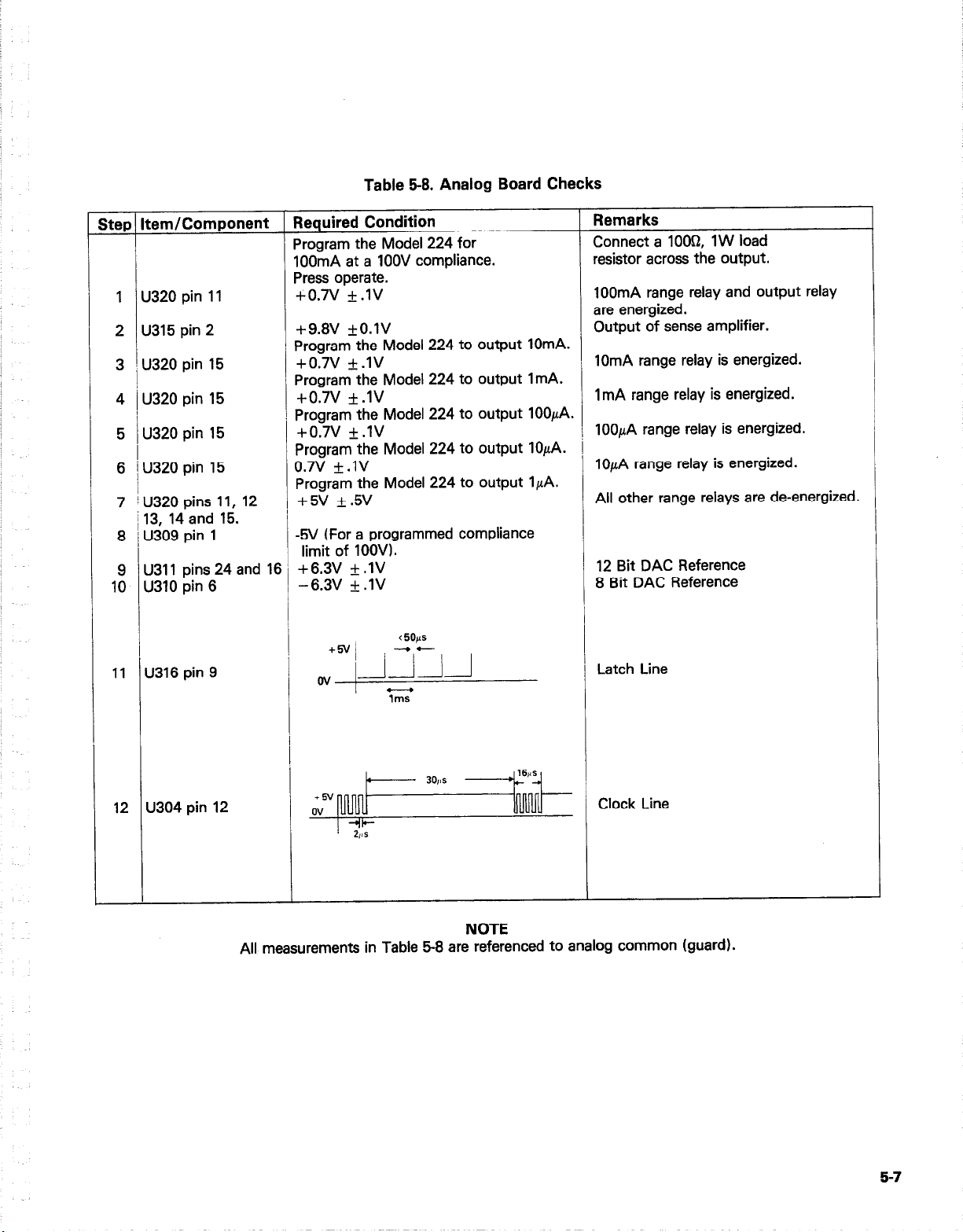
Table 58. Analog Board Checks
itep Item/Component
Required Condition
Program the Model 224 for
IOOmA at a 1OOV compliance.
Press operate.
1 U320 pin 11
2 U315 pin 2
+O.N **IV
+9.8V +O.lV
Program the Model 224 to output lOmA.
+0.7v +.lV
3 i u320 pin I5
4 / U320 pin 15
Program the Model 224 to output ImA.
+0.7v +.lV
Program the Model 224 to output 100p.A.
5 U320 pin 15
+O.N +.lV
Program the Model 224 to output lOpA. i
6 I U320 pin 15
0.7v *.lV
Program the Model 224 to output IpA.
7 jU320 pins 11, 12
+5v +.5v
113, 14and 15.
8 / U309 pin 1
-5V (For a programmed compliance
limit of 1OOV).
9 U311 pins 24 and 16 +6.3V f .lV
10 U310 pin 6
-6.3V + .lV
11 U316 pin 9
Remarks
Connect a 1 OOQ, 1 W load
resistor across the output.
100mA range relay and output relay
are energized.
Output of sense amplifier.
10mA range relay is energized.
ImA range relay is energized.
lOOpA range relay is energized.
lOpA range relay is energized.
All other range relays are de-energized.
12 Bit DAC Reference
8 Bit DAC Reference
Latch Line
12 U304 pin 12
16,~
lumr
Clock Line
+6V
ov
+I+
2,a
1
.
30,as
NOTE
All measurements in Table 5-8 are referenced to analog common (guard).
5-7
Page 46

Table 9-9. Digital Circuitry Checks
Step Item/Component
1 J1004 pins 1, 2 and 4
(referenced to pins 24,
and 26)
2 U315 pin 37
(92)
3 U115 Pin 40 (reset)
4 U114 pin 15
5 iU114 pin 39
6 / U115 pin 4, U114 pin 21
7 IUlll, UllO, u103, u105
iUlO1 and U107
/
8 /U117 pin 6 (Referenced to
/Analog Common)
10 U113 pin 3 (Referenced to
Digital Common)
Required Condition
Remarks
+5v *5% +5V Digital Supply
25
OV to 4V squarewave at 1MHz
+5v 25%
Negative going pulse ( +5V to OV) occuring
IMHz Clock
Reset Line
Strobe for display board.
every 8msec.
Negative going pulse ( +5V to OV) occuring
every lmsec
1 kHz clock
RAM and ROM (see paragraph 5.8.1 Digital
Clock input for
Display Board
IRQ Line
Digital Self Test
Self Test)
Data Out Line
(Analog Side)
Z&&x
It-
lrn?eC
Data in Line (Analog
Side)
Clock to Analog Side
l-l
+5v
0" /JLL
+ 5v
ov
11 Ul13 pin 6 (Referenced to
Digital Common)
Step Item/Component
1 Display
Required Condition Remarks
Turn on Power + 1.8.8.8.8+ 1.8
2 P1002 pins 9 and 14 + 5V +5%
3 U203 pin 1
4 U203 pin 8
1msec
Latch Enable
Table 5-10. Display Board Checks
All display segments and LEDs will
light for several seconds.
If low, check per Table 5-7.
Update Data
Clock.
5-8
Page 47

SECTION 6
REPLACEABLE PARTS
6.1 INTRODUCTION This section contains replacement parts information,
schematic diagrams and component location drawings for
the Model 224. An illustration of the fan assembly is shown in
Figure 6-l.
6.2 PARTS LIST Parts are listed alphabetically in order of their circuit designa-
tions. Table 6-l contains an index of the schematic diagrams
and component location drawings. Table 6-2 contains a parts
list for the Model 224 mother board. Table 6-3 contains a
parts list for the display board. Table 6-4 contains a parts list
for the analog board.
Table 6-1. Index of Model 224 Schematics and
Component Layouts
Title
Display Board Component Layout
Mother Board Component Layout
Analog Board Component Layout
Display Board Schematic
Mother Board Schematic
Analog Board Schematic
i
6.3 ORDERING INFORMATION
To place an order, or to obtain information concerning
replacement parts, contact, your Keithley representative or
the factory. See the inside front cover for addresses. When
ordering include the following information:
1. Instrument Model Number
2. Instrument Serial Number
3. Part Description
4. Circuit Description (If applicable)
5. Keithley Part Number
If an additional instruction manual is required, order the
manual package (Keithley Part Number 224-901-00). The
manual package includes an instruction manual and all pertinent addenda.
6.4 FACTORY SERVICE If the instrument is to be returned to the factory for service,
complete the service form which follows this section and
return it with the instrument.
6.5 SCHEMATIC DIAGRAMS AND COMPONENT
LOCATION DRAWINGS
Schematic diagrams and component location drawings
follow the replaceable parts list in the order listed in Table 6-l.
6-I
Page 48

PROTECTIVE CAP
(WHTI’
BP-II-9
-CS-287-3
TRIAX CONNECT<
ASSEMBLY
228-317 ’
FILTER , ’
(BNC) CONNECTOR
cs-249 (2)
I I \
BUSHING
I
BU-19
FAN
228-319
-REAR PANEL
CS-254
\
FH-25 (FOR 3AG SIZE)
FH-28 (FOR 5mm SIZE)
WASHER
WA-12
228-308
IGiN)
BP-116
NOTE: Mechanical parts that are replaceable show the appropriate part number. The parts that are labeled but
do not have a part number are shown for reference purposes only.
\
FILTER SUPPORT
ASSEMBLY
228-313
Figure
6-1. Fan Assembly
IEEE COVER
N”LE~OwN
6-2
Page 49

Table 6-2. Mother Board, Parts List
Circuit
Desig.
AT101
AT102
AT103
AT104
Cl01
Cl02
Cl03
Cl04
Cl05
Cl06
Cl07
Cl08
Cl09
Cl10
Cl11
Cl12
Cl13
Cl 14
Cl15
Cl16
Cl17
Cl 18
Cl19
Cl20
Cl21
Cl22
Cl23
CR101
CR102
CR103
CR104
CR105
CR106
CR107
CR108
CR109
CR110
CR111
CR112
FIOI
FlOl
FIOI
FlOl
JlOOl
J1003
J1008
P1004
P1005
PI006
Description
Optical Isolator, 6N137
Optical Isolator, 6N137
Optical Isolator, 6N 137
Optical Isolator, 6N137
.lpF, 16V, Ceramic Disc
.lpF, 16V, Ceramic Disc
lOpF, 25V, Aluminum Electrolytic
68OOpF, 5OOV, Ceramic Disc
.lpF, 16V, Ceramic Disc
.OlpF, 5OOV, Ceramic Disc
lO,OOO~F, 25V, Aluminum Electrolytic
.lpF, 16V, Ceramic Disc
.lpF, 16V, Ceramic Disc
.lpF, 16V, Ceramic Disc
.lpF, 16V, Ceramic Disc
.lpF, 16V, Ceramic Disc
.lpF, 16V, Ceramic Disc
22pF, IOOOV, Ceramic Disc
22pF, lOOOV, Ceramic Disc
.lpF, 16V, Ceramic Disc
33OpF, lSQV, Aluminum Electrolytic
33OpF, 16OV, Aluminum Electrolytic
lOpF, 25V, Aluminum Electrolytic
lOpF, 25V, Aluminum Electrolytic
IOOOpF, 35V, Aluminum Electrolytic
IOOOpF, 35V, Aluminum Electrolytic
33OpF, 5OOV, Ceramic Disc
Rectifier Bridge (5A), PE05
Rectifier, 1 N4006
Rectifier, 1 N4006
Rectifier, 1 N4006
Rectifier, 1 N4006
Rectifier, 1 N4006
Rectifier, 1 N4006
Rectifier Bridge (1.5A), PF-40
Rectifier, 1 N4006
Rectifier, 1 N4006
Rectifier, 1 N4006
Rectifier, 1 N4006
Fuse, 3/8 Amp, 25OV, Slo-Blo
Fuse, 314 Amp, 25OV, Slo-Blo
Fuse, 8/10 Amp, 25OV, Slo-Blo
Fuse, 4/10 Amp, 25OV, Slo-Blo
Fuse Holder, Line Power Fuse
Power Connector
Cable Assembly (26-pin)
Socket 16-pin
5OOV, Connector Male (for IEEE Board)
2 pin, Connector
3 pin, Molex Connector (for External Trigger)
Location
Pcb
ich
Gl D4
G3 D4
G2 D5
G3 D5
E4’ D2
G4 D2
D4 D2
F5 D2
E5
84
C4 G3
F2 D3
:: :4”
G3 E4
G2 E5
Bl C5
83 C5
83 C5
G3 E5
D2 E5
C2 E5
D3 F5
D3 F6
c3 F6
D3 F6
C4 G3
i/B1 G2
;i
F5 E3
C2 F4
C2 E4
C2 E4
C2 E4
C3 F5
C3 F5
C3 F5
G5 E3
E3
:: E3
G5 -
A4 H3
A4 H3
A4 H3
A4 H3
-
A4 G2
H5 -
H5 D2
G3
-
E5
-
83
(eithley
‘art No.
c-292
c-292
c-292
c-292
Z-238-. 1
Z-238-. 1
:-314-10
I-22-.0068
Z-238-. 1
z-22-.01
Z-342-1 0000
Z-238-. 1
Z-238-. 1
Z-238-. 1
Z-238-. 1
Z-238-. 1
Z-238-. 1
2-64-22~
Z-64-22~
Z-238-. 1
z-337-330
c-337-330
c-314-10
c-314-10
c-309-1 000
c-309-1 000
C-22-330~
RF-48
RF-38
RF-38
RF-38
RF-38
RF-38
RF-38
RF-46
RF-38
RF-38
RF-38
RF-38
FU-18
FU-19
FU-52*
Fu-53*
FH-21
CS-338
CA-103
SO-65
CS-389-3
CS-288-2
CS-288-3
6-3
Page 50

Table 6-2. Mother Board, Parts List (Cont.)
Circuit
Desig.
RlOl
R102
R103
R104
R105
R106
R107
R108
R109
RllO
Rlll
R112
R113
R114
Rll5
RI18
R119
R121
R122
R125
R126
RI27
R128
SlOl
s702
TlOl
TlOl
UlOl
u102
u103
u104
u105
U106
u107
U108
u109
UllO
Ulll
u112
u113
u114
u115
U116
u117
VR101
VR102
VR103
WlOl
WI02
YIOI
*For use with special factory installed transformer TR-187.
**Order same software as presently installed. For exatiple if B5 is displayed on power-up, order 224-800-85 for
u109.
***Order heat sink mounting kit (MK-18) and heat sink (HS-15) with these parts.
tOrder heat sink mounting kits (MK-16 and MK-20) and heat sink (HS-22) with this part.
Description
18k, 5%, 1/4W, Composition
4.7k, 5%, 1/4W, Composition
220k, 5%, 1/4W, Composition
4.7k, 5%, 1/4W, Composition
3900, 5%, 1/4W, Composition
22OQ, 5%, 1/4W, Composition
2.4k, 5%, 1/4W, Composition
22OQ, 5%, 1/4W, Composition
2.4k, 5%, 1/4W, Composition
2203, 5%, 1/4W, Composition
2.4k, 5%, 1/4W, Composition
4.7k, 5%, 1/4W, Composition
2203, 5%, 1/4W, Composition
Thick Film Resistor Network
4.7k, 5%, 1/4W, Composition
lOOk, + lo%, 1/2W, Composition
lOOk, f lo%, 1/2W, Composition
10052, + IO%, 1/2W, Composition
1OOQ + lo%, 1/2W, Composition
4.7k, 5%, 1/4W, Composition
IOk, 5%, 1/4W, Composition
4.7k, 5%, 1/4W, Composition
47kQ, lo%, 0.25W, Composition
Switch, Power
Switch, Line Voltage Selection
Transformer
Transformer (special for 9OV-1 IOV 18OV-220V operation)
1024 x 4-bit Static RAM, 2114
Oscillator/Clock, 4060
1024 x Qbit Static RAM, 2114
Up/Down Counter, 74LS193
1024 x Cbit Static RAM, 2114
Quad 2-In. Nand Gate, 74LSO0
1024 x 4-bit Static RAM, 2114
Quad 2-In. NOR Gate, 74LSO2
Erasable Prom, 2732
DecoderlDemultiplexer, 74LS138
Erasable Prom, 2732
8-bit Shift Register, 14094
Quad Exclusive OR Gate, 7486
Interface Adapter, SY6522
Microprocessor, MC6808
Bus Driver, 14503
Hex Inverter, 16-pin DIP, 4049
5V Regulator, LM309K
f 15V. 3-term, 7915
3-term Positive Voltage Regulator, 7815
Jumper
Jumper
4.0 MHZ Crystal
Location
Sch Pcb
F4
Fl
c4
F2
2
G3
G2
G2
G2
G2
Hl
Gl
E5
F3
D2
D2
G5
G4
E2
Fl
G4
G5
A3
A3
82
82
D5
E4
c5
F4
iii
SEV
SEV
B5
F3
A5
SFV
c2
B2
E6
SEV
D4
D3
D3
B6
B6
-
D2
D3
F3
E4
E4
D4
E4
D5
E5
D5
E5
E5
E5
B5
c5
E5
E5
E3
E3
D4
D5
E3
E3
B2
G2
F2
F2
c2
D2
c2
::
D2
c3
D3
c3
::
D4
::
c5
c5
E5
F4
F5
F5
D2
D2
c5
Keithley
Part No.
R-76-18k
i-76-4.71<
R-76-220k
R-76-4.7k
R-76-390
R-76-220
R-76-2.4k
R-76-220
R-76-2.4k
R-76-220
R-76-2.4k
R-76-4.7k
R-76-220
TF-140
R-76-4.7k
R-l-look
R-l-look
R-1-100
R-1-100
R-76-4.7k
R-76-10k
R-76-4.7k
R-76-47k
SW-426
SW-397
TR-186
TR-187
LSI-15
IC-197
LSI-15
IC-214
LSI-15
IC-163
LSI-15
IC-179
224-800-**
IC-182
224-801-**
IC-251
IC-116
LSI-28
LSI-27
IC-250
IC-106
IC-98t
IC-174***
IC-96***
J-3
J-3
CR-10
6-4
Page 51

Table 6-3. Display Board, Parts List
Circuit
Desig.
c201
DS201
DS202
DS203
DS204
DS205
DS206
DS207
DS208
DS209
DS210
DS211
DS212
DS213
DS214
DS215
DS216
DS217
DS218
DS219
P1002
0201
Q202
Q203
0204
Q205
Q206
0207
0208
R201
R202
s201
s202
S203
S204
S205
S206
S207
S208
5209
s210
s211
s212
S213
S214
S215
S216
S217
S218
s219
s220
Description
IOpF, 25V, Aluminum Electrolytic
+ 1, Digital Display
“8” Digital Display
“8” Digital Display
“8” Digital Display
“8” Digital Display
+ 1, Digital Display
“8” Digital Display
Pilot Light
Pilot Light
Pilot Light
Pilot Light
Pilot Light
Pilot Light
Pilot Light
Pilot Light
Pilot Light
Pilot Light
Pilot Light
Pilot Light
Cable Assembly
PNP Silicon Transistor, 2N4355
PNP Silicon Transistor, 2N4355
PNP Silicon Transistor, 2N4355
PNP Silicon Transistor, 2N4355
PN P Silicon Transistor, 2N4355
PNP Silicon Transistor, 2N4355
PNP Silicon Transistor, 2N4355
PNP Silicon Transistor, 2N4355
Thick Film Resistor Network
Thick Film Resistor Network
Pushbutton Switch
Pushbutton Switch
Pushbutton Switch
Pushbutton Switch
Pushbutton Switch
Pushbutton Switch
Pushbutton Switch
Pushbutton Switch
Pushbutton Switch
Pushbutton Switch
Pushbuton Switch
Pushbutton Switch
Pushbutton Switch
Pushbutton Switch
Pushbutton Switch
Pushbutton Switch
Pushbutton Switch
Pushbutton Switch
Pushbutton Switch
Pushbutton Switch
Location
Sch Pcb
D5 c3
Bl 82
Cl
CS
Dl c2
Dl
E1
G3
G2
z
H3
H3 c2
F3
F3 D2
:i :
H3 c3
F3 D3
A6 E4
F5 El
H5 El
H5
H5
LE z
iii:
SEV D2
SEV
A3 B2
B3 B2
B3 c2
A3
A3
84 E2
iti
A4
84 E
84 D3
A4 E3
A4 E3
85
B5
2
A3 F2
83
83 F3
82
c2
D2
D2
E2
z
E2
B2
82
D2
El
El
E2
I3
Fl
D2
D2
E2
B3
F2
F2
G2
F2
G2
Keithley
Part No.
C-314-10
DD-31
DD-20
DD-20
DD-20
DD-20
DD-31
DD-20
PL-67
PL-67
PL-67
PL-67
PL-67
PL-67
PL-67
PL-67
PL-67
PL-67
PL-67
PL-67
CA-15-1
TG-90
TG-90
l-G-90
TG-90
TG-90
TG-90
TG-90
TG-90
TF-165-1
TF-77
SW-435
SW-435
SW-435
SW-435
SW-435
SW-435
SW-435
SW-435
SW-435
SW-435
SW-435
SW-435
SW-435
SW-435
SW-435
SW-435
SW-435
SW-435
SW-435
SW-435
6-6
Page 52

Table 63. Display Board, Parts List (Cont.)
Circuit
Desig.
s221
s222
S223
S224
S225
u201
u202
U203
U204
Description
Pushbutton Switch
Pushbutton Switch
Pushbutton Switch
Pushbutton Switch
Pushbutton Switch
MOS to LED Segment Driver, 75492
MOS to LED Segment Driver, 75492
B-bit Shift Register, 74LS164
MOS to LED Seament Driver. 75492
Location
Keithley
Sch Pcb Part No.
A2 F3
A2 G3
82 F3
SW-435
SW-435
SW-435
SW-435
E 2
SEV 83
SEV c3
C5 D3
SEV E3
SW-435
IC-169
IC-169
IC-127
IC-169
6-6
Page 53

Table 64. Analog Board, Parts List
Circuit
Desig.
c301
C302
c303
c304
c305
C306
c307
C308
c309
c310
c311
C312
c313
c314
c315
C316
c317
C318
c319
C320
C321
C322
C323
C324
C325
C326
C327
C328
c329
c330
CR301
CR302
CR303
CR304
CR305
CR306
CR307
CR308
CR316
CR317
J1003
K305
K306
K307
Q301
Q302
G303
Q304
Q305
Q306
Q307
Description
,lhF, 16V, Ceramic Disc
,lpF, 16V, Ceramic Disc
,lpF, 16V, Ceramic Disc
.OlpF, 5OOV, Ceramic Disc
.47pF, 5OV, Ceramic Film
47OpF, lOOOV, Ceramic Disc
,OlpF, 5OOV, Ceramic Disc
.02pF, 5OOV, Ceramic Disc
.02pF, 5OOV, Ceramic Disc
47OpF, lOOOV, Ceramic Disc
.OOlpF, 5OOV, Ceramic Disc
lO,uF, 25V, Aluminum Electrolytic
.OOlpF, 5OOV, Ceramic Disc
lOpF, 5OOV, Polystyrene
lOpF, 25V, Aluminum Electrolytic
lOpF, 25V, Aluminum Electrolytic
4.7pF, 35OV, Aluminum Electrolytic
.OlpF, 5OOV, Ceramic Disc
.lpF, 16VDC, Ceramic Disc
.OOlpF, 5OOV, Ceramic Disc
.llF, 16VDC, Ceramic Disc
.OlpF, 5OOV, Ceramic Disc
4.7pF, 35OV, Aluminum Electrolytic
lOpF, 25V, Aluminum Electrolytic
lOpF, 25V, Aluminum Electrolytic
O.lpF, 25OV, Metalized Polyester
lOpF, 25V, Aluminum Electrolytic
.OlpF, 5OOV, Ceramic Disc
.OlaF, 5OOV, Ceramic Disc
1.5pF, 25V, Aluminum Electrolytic
Diode, Germanium, 1 N3592
Silicon Diode, 1 N914
Silicon Diode, 1 N914
Diode Dual, Low Leakage, 10101
Rectifier, 1 N3595
Rectifier, 1 N3595
Silicon Diode, 1 N914
Silicon Diode, 1 N914
Silicon Diode, lN914
Silicon Diode, 1 N914
Connector, Male
Relay
Relay
Relay
N-Channel FET, 2N4393
N-Channel FET, PF5301
N-Channel FET, 2N4392
N-Channel FET, 2N4392
N-Channel FET, 2N4392
N-Channel FET, 2N4392
N-Channel FET, 2N4392
Location
Sch Pcb
F3 B2
E3 B2
C2 Dl
84 Dl
A4 D2
C3 D2
F5 82
F4 B2
E2 c2
c2 c3
Bl 83
Dl B3
D2 B3
D3 83
C5 D4
C4 04
F3 F3
F2 E4
E4
: E4
E2 E5
Fl F5
Fl F5
B6 D5
B6 D5
B4 D4
B6 D4
E
G4 D5
SEV 85
SEV 85
SN 85
iii
c2
I2
C3 D3
03
g 83
D3 B4
Ii: E
84 D4
F2 F4
Fl F5
B2 D5
El 83
Dl 83
E4 C3
F4 C3
c3
: D3
F4 C3
(eithley
Part No.
Z-238-s 1
C-238-m 1
Z-238-. 1
C-22-.01
C-237-.47
2-64-470~
C-22-.01
C-22-.02
C-22-.02
C-64-470~
c-22-.001
C-314-10
c-22-.001
C-138-10~
c-314-10
c-314-10
C-240-4.7
c-22-.01
C-238-. 1
c-22-.001
C-238.1
c-22-.01
C-240-4.7
c-314-10
c-314-10
C-178-0.1
c-314-10
c-22-.01
c-22-.01
c-314-1.5
RF-39
RF-28
RF-28
DN-3
RF-43
RF-43
RF-28
RF-28
RF-28
RF-28
CS-3893
RL-70
RL-70
R L-50
TG-130
TG-139
TG-128
TG-128
TG-128
TG-128
TG-128
6-7
Page 54

Table 6-4. Analog Board, Parts List (Cont.1
Circuit
Desig.
0308
a309
Cl310
Cl311
0312
Q313
0314
0315
Q316
Q317
0318
Cm9
R301
R302
R303
R304
Description Sch Pcb Part No.
N-Channel FET, 2N4392 F4
N-Channel FET, 2N4392
N-Channel FET, 2N4392 G4
NPN-Power Transistor, 2N5190
PNP-Power Transistor, 2N5193
PNP, Transistor, Silicon, 2N3906 E3 E4 TG-84
PNP, Transistor, Silicon, 2N3906
NPN, Silicon, 2N3904
Diode Current Unit, J505
NPN, Silicon, 2N3904
PNP, Transistor, MJ5012
NPN, Transistor, MJ5011
301 k, 1 %, 1/8W, Metal Film
lM, l%, O.l2W, Metal Film
100k Pot
1OOk Pot
R305 49.9k, 1%, 1/8W, Metal Film
R306
lOk, 1%, 1/8W, Metal Film
R307 6.04k, 1%, 1/8W, Metal Film
R308
R309
R310
R311
47k, 5%, .1 lW, Thick Film Resistor E5 82 TF-103-4
47k, 5%, .llW, Thick Film Resistor
47k, 5%, .llW, Thick Film Resistor
47k, 5%, .llW, Thick Film Resistor Dl C2 TF-103-4
R312 lOk, 5%, 1/4W, Composition
R313 1 k, 5%, 1/4W, Composition
R314 20k, 5%, 1/4W, Composition
R315 2.2k, 5Oh, 1/4W, Composition
R316
301 k, 1%, 1/8W, Metal Film F5 82 R-88-301 k
R317 22.2k, .l%, l/lOW, Metal Film
Location
Keithley
C3 TG-128
F4
C3 TG-128
D3
TG-174
D5
D3 TG-108
D4 TG-107
. D5
F2 F4 TG-84
E2
E5 TG-47
El F5 TG-140
E5 TG-47
E
E5 TG-155”
F3 E4 TG-154*
F5 B2 R-88-301 k
82 R-88-1M
zi Bl RP-97-100k
G5 82 RP-97-1OOk
82 R-88-49.9k
ii: 82 R-88-10k
F5 82 R-88-6.04k
D5 C2 TF-103-3
D4
C2 TF-103-3
Dl R-7610k
E D2 R-76lk
c4
D2 R-7620k
G3 D2 R-76-2.2k
F4
B2 R-263-22.2k
R318 2000 Pot F4 83 R P-97-200
R319
R320 22.2k, I%, 1 IlOW, Metal Film
R321 20k, 1%, 1/8W, Metal Film E
2k Pot E2 83 R P-97-2k
C2 R-263-22.2k
C2 R-88-20k
R322 20k, 1 %, 1/8W, Metal Film C3 R-88-20k
R323 Ilk, l%, 1/8W, Metal Film
zi
C2 R-88-l 1 k
R324 lOk, 5%, 1/4W, Composition C3 R-7610k
R325 20k, 5%, 1/4W, Composition :i C3 R-7620k
R326 1 k, 5%, 1/4W, Composition c3 C3 R-76lk
R327 lOk, 5%, 1/4W, Composition 82 C3 R-7610k
R328
R329 4.99k, 1 %, 1/8W, Metal Film
R330
R331
R332 1 M, 5%, 1/4W, Composition
R333 1 k, 5%, 1/4W, Composition ::
1 k, 1 %, 1/8W, Metal Film E2
B2
1 M, 5%, 1/4W, Composition
4.99k, l%, O.l2W, Metal Film
c2
83 D2 R-88-4.99k
C2 R-8Blk
D2 R-88-4.99k
D2 R-761M
D2 R-761M
D3 R-76lk
R334 IOOQ, 5%, 1/4W, Composition D3 R-76100
R335 4700, 5%, 1/4W, Composition ii: 03 R-76470
R336
4.7k, 5%, 1/4W, Composition
F5 C3 R-76-4.7k
R337 4.7k, 5%, 1/4W, Composition C3 R-764.7k
R338 24k, 5%, 1/4W, Composition E 83 R-7624k
R339 390, 5%, 1/4W, Composition Cl 83 R-7639
R340 393, 5%, 1/4W, Composition c2
83 R-76-39
6-B
Page 55

Table 6-4. Analog Board, Parts List (Cont.)
Circuit
Desig .
R341
R342
R343
R344
R345
R346
R347
R348
R349
R350
R351
R352
R353
R359
R360
R363
R364
R365
R366
R367
R368
R369
R370
R371
R372
R373
R374
R375
R376
R377 20k, l%, O.l2W, Metal Film 2
R379
R380
R381 IOOD, 0.1 %, 3W, Fixed
R382 49.9k, I%, O.l2W, Metal Film
R383
R384 5k, Pot
R385 500 Pot
R386 IOk Pot
R387 lk Pot
R388
R389
R390
R391
R392
R393
u301
U302
u303
u304
u305
U306
u307
U308
u309
Description
24k, 5%, 1/4W, Composition c2
Ik, 5%, 1/4W, Composition E2
IOk Pot
IOk, 5%, 1/4W, Composition
470k, 5%, 1/4W, Composition E2
47k, 5%, 1/4W, Composition
15k, 5%, 1/4W, Composition
2,4k, 5%, 1/4W, Composition
IOk, I%, O.l2W, Metal Film
IOOk, .I 1 W, Thick Film Resistor
IOk, 5%, 1/4W, Composition A4
IOk, 5%, 1/4W, Composition A4
2.2M, IO%, 0.25W, Composition B4
IOOk, I%, 1/4W, Composition D3 C4 R-88-100k
1 k, 1 %, 1/4W, Composition D3 C4 R-76-lk
2.2k, 5%, 1/4W, Composition E3
24k, 5%, 1/4W, Composition
lOOk, 1%, 1/2W, Metal Film
lOOk, l%, 1/2W, Metal Film
lOB, l%, O.l2W, Metal Film G2
133, 1%, O.l2W, Metal Film G2
220, IO%, 1/2W, Composition
22B, IO%, 1/2W, Composition
2.2k, 5%, 1/4W, Composition
130, 1%, 1/8W, Metal Film
IOQ, I%, O.l2W, Metal Film Gl
4.7k, 5%, 1/4W, Composition E2
54.lk, .I%, IIIOW, Metal Film
4.93k, .l%, IIIOW, Metal Film
485k, .I %, 1/4W, Metal Film
4990, .l %, 1/25W, Metal Film G4
3.57k, I%, O.l2W, Metal Film
IOOk, 5%, 1/4W, Composition
IOk, 5%, 1/4W, Composition
IOk, 5%, 1/4W, Composition
IOk, 5%, 1/4W, Composition 83
10k Pot
3.9k, 5%, 1/4W, Film or Composition E2
Shit Shift Register, 14094
8-bit Shift Register, 14094
8-bit Shift Register, 14094
Quad 2-input AND, 4081 SEV D2 IC-138
Quad 2-Input NAND, 4011 SEV D2 IC-102
Quad Monolithic SPST CMOS Analog Switch, LM317T SEV C2 IC-320
Wide Bandwidth Dual JFE’T, LF353N E5
CMOS 8-bit Multiplying D/A Converter, AD7523 I2
Wide Bandwidth Dual JFET, LF353N
Sch Pcb Part No.
SE C3 TF-103-2
Location Keithley
B3 R-76-24k
83 R-76-lk
B3 RP-97-IOk
B3 R-76-IOk
iis
83 R-76-470k
Bl ’ B3 R-76-47k
83 R-76-l 5k
Bl
B3 R-76-2.4k
Dl
83 R-88-10k
D3 R-76-10k
D3 R-76-IOk
D4 R-76-2.2M
E4 R-76-2.2k
E4 R-76-24k
E3
F4 R-94100k
c3
F4 R-94100k
83
F4 R-88-10
F4 R-88-13
F4 R-l-22
Fl
F2 F5 R-l-22
E5 R-76-2.2k
El
F5 R-88-13
Gl
F5 R-88-10
E5 R-76-4.7k
D5 R-263-54.1 k
F3
D5 R-263-4.93k
C5 R-88-20k
C4 R-264-485k
F3
C5 R-286499
C5 R-308-100
G4
C5 R-88-49.9k
G5
D5 R-88-3.57k
G3
F4
C5 RP-955k
C5 RP-97-500
C5 RP-97-IOk
Ei
G4
D4 D5 R-76-100k
C5 RP-97-1 k
D5 R-76-10k
83
84 D5 R-76-IOk
D5 R-76-IOk
F4 83 RP-97-IOk
D4 R-763.9k
C4 Bl
c3
c2
E2
IC-251
Cl IC-251
Cl IC-251
C2 IC-246
C2 IC-321
C2 IC-246
6-9
Page 56

Table 6-4. Analog Board, Parts List
Circuit
Desig.
u301
Description
Operational Amplifier, AD3247
Location
Keithley
Sch Pcb Part No.
El c2 IC-77
u311 Integrated Circuit D/A Converter, DAC80-CBI-V E4 82 IC-323
U312 Operational Amplifier, AD3247
~ F4 B3
IC-248
u313 Quad Comparator, LM339 SEV B3 IC-219
u314 Quad 2 Input NAND, 4011 SEV c3 IC-102
u315 Operational Amplifier, AD3247 84 c3
U316
u317
U318 Decoder/DemuItiplexer, 14555
Hex Inverter, 16-Pin, 4049
Quad Comparator, LM339
SEV D3 IC-106
SEV C3 IC-219
SEV C3 IC-312
u319 Op Amp, AD515K D2
U320
High/Voltage, High/Current Transistor Array, VLN2003A
c5
VR301 +5V Regulator, 7805 B6
G-77
B3 IC-241
C3 IC-206
D5 IC-93
*Order heat sink (HS-22) and heat sink mounting kits (MK-16) and (MK-20) with these parts.
6-10
Page 57

1 5214 1 1 5215 1 1 5216 11
Ii-3
3
f
.3MMAMAI,huM I
0
DS211
(9DS212 aDS213 aDS214 oDS215 oDS216 aDS217
SCHEM.
RT No. ~CC,C
c
1 ZONE 1 1 ITEM 1 FART NO. 1 ;
IGZ I
I
I
I
/ 5217 I/ 5218 / 1 S219 11
r‘L-L7
,$, 23
MK-Z/-/
OS2/3 03
IZEab -
Figure 6-2. Display Board, Component Location Drawing,
Dwg. No. 220-110
Page 58

T lOI
I;lX&ED Cl2ltCli2 b
2
EL lmltm
R
7-m-
--L-l,\
LT/ 043) INSTALL BETWEEN
-~4Jl
-‘-+-‘+“X-,BrniLLlr~ -Lilu
/ HEA SCREW
7 DCnlrlDrn
IM=t,. CeN
NOTES
I)UiOY ISLSI-I5
USE WI01
3)TIOI ISTRl86
.C~NNECT ~~HITE/BROWN
TO POINT x
‘A
“-COMPONENT t.AYOUl
MCI HER BMHD
4
5
- 6
Figure 6-3. Mother Board, Component Location Drawing,
Dwg. No. 220-100 (sheet 1 of 2)
6-131814
Page 59

ITEM
j I
PART NO
/ ITEM 1
PlRT NO.
/ ZONE /
-
3
-I
4
*NOTES:
IIFOR IOOVJAPANESE VERSION
SuBST I TUTE ITEM 95ITR-1871
FnQ ITEM94lTR-1861.
I..
2)FOR EUROPEAN VERSION
SUBSTITUTE FL’-50 AND FU-51
FOR FU-4 ANC FU-I% AL3
~UI~STITUTE FH-ZC FOR
FH-25.
SOFTWARE SELECTION TABLE
n
SCHEMATIC
iTEM
DESIGNATION
105 LJIW
107 Ll//l
MODEL 220
220-8~0 ZZLJ SDD
220 -801
USAGE
MODEL 230 MODEL 224
USAGE
-
230- 80/ 224 -801
USAGE
224 -800
L
M
t
4
--
5
-6
”
Figure 6-3. Mother Board, Component Location Drawing,
Dwg. No. 220-100 (sheet 2 of 2)
6-15/6-16
Page 60

I
1
B
C
D
4
E
I
F
-
--
G H
1
-
2
-
3
-47-i
4
-
5
-
6
NOTE :
NOT STRESS LEADS
DO
CR305
OF
AND 07306.
(c317)
Figure 8-4. Analog Board, Component Location Drawing,
Dwg. No. 224-120 (sheet 1 of 2)
8-17/8-18
Page 61

Figure 6-4. Analog Board, Componet Location Drawing,
Dwg. No. 224120 (sheet 2 of 21
6-1919-20
Page 62

1
ws:
I. ALL RESISTOR VALUES ARE IN OHMS
-
:
-
4
-
5
UNLESS MARKED OTHERWISE.
(K-KILOHYS~
2. ALL CAPACITOR VALUES ARE IN
MICROFARADS.
30 DENOTES FRONT PANEL CONTROL.
4.Q DE+NFJ_TES DIGITAL COMMON.
XFONENT
ENTER _
COPY
8 _
3E.215
I
_ OPERATE B
DS201
a=
6 -
t.3 4
u
n - PLUS 2 UJ
n
9
l”“5 ’
5
0 -0
uzozc
5
(PO)
U2028
31 41
QA
‘1 j
DATA
A CLOCK
I .I II ,411 ?I bl
DS202
QB
__
OS203
4,
(f,) (X2) (I,)
51
‘1,
U203 SHIFT REGISTER
GND VCC B CLEAR
DS204
61
Q~
DATA
I01 III
QE
QF
OS207 d 7 1 1
I21 I31
QG QH
QZC
9
OFERATE~
D’S213
przzol/,
V-LIMIT
OS215
RZOIA
Go
LISTENn
DSZOY
SINGLE”
DSZII
:ZOIG
I50
:201s
I50
5
1
TAR@0
DSZIY
‘STEP ‘/
DS213
.tOlE
I50
2
l2OlF
IM
-
‘too;
I3
6
HIGHEST SCHEMATIC
DESIGNATIONS USED
CZOI 1 DSZIY 1 Q208
R202 I 5225 I u204
PlOO2 I
ml ns,n .IYC
-a- - - -
54
-------&----.;t-.--
PB5
CA2
--<am--z&----- ----------------- ----
DIGITAL
COMMON
+5v
kw
PA4 PA7
I91
(0
PA0
Id)
PAZ
(Cl
PAI
6
SCHEMATT$ WSI~NATIONS
Jl002 1
PIOOI I
I
A
I
I
I
I
I
B
I
C
I
D
T
E
I
F
I
G
I
Ii
Figure 6-5. Display Board, Schematic Diagram,
Dwg. No. 226-116
Page 63

NOTES:
I. ALL RESISTOR VALUES ARE IN OHMS
UNLESS MARKED OTHERWISE.
(K-KILOHMS)
2. ALL CAPACITOR VALUES ARE IN 0
MICROFARADS. I PLUSP 2 4 ,u
30 DENOTES FRONT PANEL CONTROL.
DENOTES DIGITAL COMMON.
4.@ +,-
_.
DSZOI
u
a.6
b3 4
u
inus
0 -0
6
I
‘U 17
r
I
u
u-0
u u
‘0
dP
3 5 3 5 3 5 3 5
dp
-
4 ,u
c u
-0
dp
dp
,. ,-
b
.6
c4
d-2 e
P ’
f9
9 ‘0
1
-
I
t
nnrn IT,- , , 1 , , ,
“r;nT+,c (
I A,-... I I
A,..., A--.- A# /r,
, ”
Tkk-t i ”
I
U2Ol+ U2OlE+ +s;~&
4
QB
u203 SHIFT REGISTER
I I I III I
5 6
QC
0
QD
IO II
QE
QF
I2
I
QG
“DECR”
DS219
I
I _ I _ I
1 v $RZOIA (RZOID iR20lC 1RtOlH (RtOlG $RtOlB $RZOlE (Fi
I($,) ‘7 916 913 914 99 910
t Ii Ii Ii
*LISTEN’
OS203
I I I I
+I2
03
120lF
I50
DATA
A
CLOCK
_ - - - ----
51 52 53 54 PB5 CA2 DIGITAL +5v
I
I
C
COMMON
I
DATA
o+sv
---- ------- -----------_
(d) ‘r’,
PA4 PA7
D
T
E
I
F
I
-. -
G
I
(a) PA5
H
Page 64
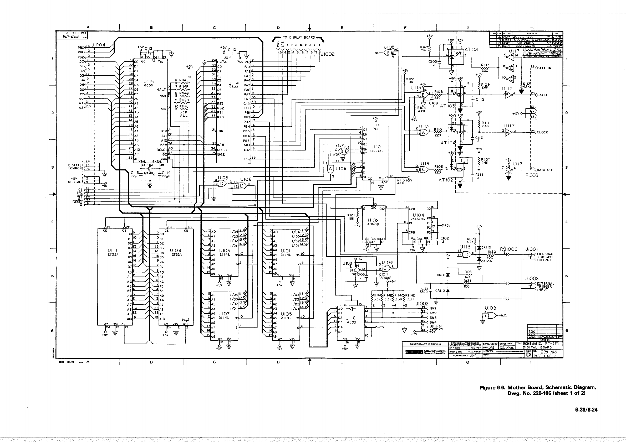
1
-
2
I
-
3
2 30 I 33Wd
%I-ozz 011
pBo<~4 J1004
A
I
B
I
C
I
\ ~-0 DISPLAY i3OARD\
D
E F
+5V
?
G
I REVXDN
H
I
RN4GI
I’llI I
D6
07
RS3
RS2
RSI
RSO
PB4 I4
“‘I JIII I I ! 1
+5v
P
I J6 1
II I
-Ul13
lJll7
+
4
I8 20
CE OE
DO
\
\
\
\
\
\
\
\
\
\
\
\
\
\
\
A5 21 14L W
\
A5 2114L W
\
6
\
P-
UlO8
3
2
N.C.
Figure 6-6. Mother Board, Schematic Diagram,
Dwg. No. 220-106 (sheet 1 of 2)
6-23/6-24
Page 65

=
#I I
r$2J=J; y&Frw
L-------J L-------J
“TY”
Page 66

@I
I
m
n I
k=----HIIIlI
I I I I I I I
’ It I I I I
I
I
-_
!
”
b
T
-i
u-l
T
>
0
in
>
T
Page 67

,
-
R347
ISK
R33>
39
R340
R372
:
R370
R36d
2
-
E37E
4 33K
KX)6
I =uuut
P/J1009
JiOl3
3
: -8
U318.4
U32OD
U32OF
-1.-
NC
K305
f5V
+5v?,F
EN
+5v-
R337
R33E
NOTES:
I.ALL RESISTOR VALUES ARE IN OHMS UNLESS
OTHERWISE MARKED(K-KILOHMS,H-MEGOHMS,G-GIGOHMS)
2.ALL CAPACITOR VALUES ARE IN MICROFARADS
UNLESS OTHFRWISE MARKEDcpF -PICOFARAOS).
DENOTES OUTPUT COMMON.
3.*
4q DENOTES ANALOG COMMON.
DENOTES CHASSIS CONNECTION.
‘h
~~DENOTES INTERNAL ADJUSTMENT.
Z.DENOTES REAR PANEL MOUNTING.
62 DENOTES TEST POINT.
Figure 6-7. Analog Board, Schematic Diagram,
Dwg. No. 224-126 (sheet 2 of 2)
5
6
6-2916-30
Page 68

Service Form
Model No.
Serial No.
Date
Name and Telephone No.
Company
List all control settings, describe problem and check boxes that apply to problem.
Q Intermittent
a IEEE failure
m Front panel operational
Display or output (check one)
a Drifts
a Unstable
a Overload
m Calibration only
# Data required
(attach any additional sheets as necessary)
Show a block diagram of your measurement system including all instruments connected (whether power is turned on or not).
Also, describe signal source.
m Analog output follows display
a Obvious problem on power-up
a All ranges or functions are bad
a Unable to zero
a Will not read applied input
m Certificate of calibration required
a Particular range or function bad; specify
a Batteries and fuses are OK
a Checked all cables
Where is the measurement being performed? (factory, controlled laboratory, out-of-doors, etc.)
What power line voltage is used?
Relative humidity?
Any additional information. (If special modifications have been made by the user, please describe.)
Be sure to include your name and phone number on this service form.
Other?
Ambient temperature?
“F
Page 69

Page 70

FREEPRODUCTKJPGRADEINFORMATION
To receive future information on product upgrades and enhancements,
complete this card and mail, or FAX to 440/248-6168.
MODEL
NAME
COMPANY
ADDRESS
CITY
PHONE
E-MAIL
SERIAL NO.
TITLE
MAIL STOP
STATE/PROVINCE
FAX
DATE
ZIP
For FREE additional information, check below:
Application Notes
q
General Purpose Measurements
0 Component Test Applications
Facility
(Check One)
q
K Aerospace/Defense 0 4 Calibration/Metrology
0 S Automotive/Parts Mfg. 0 6 ComponentTest
0 Q Chemical/Petroleum Processing
0 H Components Mfg. (Non-Semi)
0 N Computer/Peripherals 0 G Corp./General Mgmt.
0 T Consumer Electronics 0 7 Education
q
L Digital ICs
0 U Discrete Components 0 1 Engineering Management
q
D Displays
0 V Distributors/Resellers/Rental 0 0 Purchasing
0 F Education/University 0 8 Quality Assurance/Control
q
B Industrial Controls Mfg.
q
R Medical Equip. and Services
0 Y Mixed-Signal Components
0 2 Other Discrete Manufacturing 0 9 Service/Repair
q
0 Optoelectronic Components
0 I Process Control Industries
0 C Regulatory 0 X Other
q
E Research Laboratories
0 J Semi. Components - Other
0 1 Semiconductor Mfg.
0 2 Semi. Pkg. Part Testing
0 P Telecommunications Equip.
0 G TestiMeawement Equipment Mfg~
0 M Utility
0 4 VAR/System Integrator/Consultant
0 X Other
Reference Publications
0 Low Level Handbook
0 Switching Handbook
Job Function
0 C Consulting
0 3 Engineering Design
0 5 Mfg. Production Test
0 2 Research & Development
q
S Safety Manager
0 E System EngineeringRnlegration
0 T TestTechnician
(Check One)
Catalogs
0 Full Line Product Catalog
Product Interest(s)
0 M Acculex Digital Displays
0 G Communications Test
0 7 Current/Voltage Source
0 V C-V Measurements
0 D Data Aquisition Boards
0 R Data Acq. Test &Analysis Software
0 2 Digital Multimeters
0 L Distributed I/O
0 4 Electrometersil’icoammeters
0 A Flat Panel Display Test
0 F Function Generators
0 3 High Resistance Meters
0 E IEEEInterfaces
0 I I-V Characterization
0 N LCZ Meters
0 5 ’ Nanovoltmeters
0 B Network Measurement Modules
0 6 Ohmmeters
0 P PC Instruments
0 K Portable Products
q
8 Precision Power Supplies
0 T Semiconductor Parametric Test
0 H Serial Communication Interfaces
0 J Signal Conditioning Products
0 U Source/Measure Instruments
0 S Switching Systems/Scanners
0 0 Temperature Measurements
0 W Wafer Level Reliability
0 X Other
COUNTRY
Page 71

ES96-6E lbb HO ClNVl3A313
3NI SlN3WflI.llSNI A3lHlEl!+l
33smaav AH alvd 38 1lIM 33VlSOd
HO
ClNVMA373 6SLll. 'ON
IIVW AldalI SS3NISf-M
S31VlS a31lNf-l
3Hl
NI
a3ilvw rli
AIVSS333N
33VlSOdON
1. What other Keithley products do you currently use?
09Z t6E X09 Od
IIWBLld 1It’W SSVD-ISIH
2. What effects, devices or phenomena do you measure with this instrument?
3. What was the main reason a Keithley unit was purchased?
4. Do you have any design suggestions concerning this unit?
PLEASE RRFOLD SO YOUR NAME IS INSIDE, TAPE AND MAIL.
Page 72

Page 73

Page 74

Page 75

Specifications are subject to change without notice.
All Keithley trademarks and trade names are the property of Keithley Instruments, Inc. All other
trademarks and trade names are the property of their respective companies.
Keithley Instruments, Inc. 28775 Aurora Road • Cleveland, Ohio 44139 • 440-248-0400 • Fax: 440-248-6168
1-888-KEITHLEY (534-8453) www .keithley.com
BELGIUM: Keithley Instruments B.V. Bergensesteenweg 709 • B-1600 Sint-Pieters-Leeuw • 02/363 00 40 • Fax: 02/363 00 64
CHINA: Keithley Instruments China Yuan Chen Xin Building, Room 705 • 12 Y umin Road, Dewai, Madian • Beijing 100029 • 8610-6202-2886 • Fax: 8610-6202-2892
FRANCE: Keithley Instruments Sarl 3, allée des Garays • 91127 Palaiseau Cédex • 01 64 53 20 20 • Fax: 01 60 11 77 26
GERMANY : Keithley Instruments GmbH Landsberger Strasse 65 • D-82110 Germering • 089/84 93 07-40 • Fax: 089/84 93 07-34
GREAT BRITAIN: Keithley Instruments Ltd. The Minster • 58 Portman Road • Reading, Berkshire RG30 1EA• 0118-9 57 56 66 • Fax: 0118-9 59 64 69
INDIA: Keithley Instruments GmbH Flat 2B, WILLOCRISSA • 14, Rest House Crescent • Bangalore 560 001 • 91-80-509-1320/21 • Fax: 91-80-509-1322
ITALY : Keithley Instruments s.r.l. Viale San Gimignano, 38 • 20146 Milano • 02-48 39 16 01 • Fax: 02-48 30 22 74
KOREA: Keithley Instruments Korea 2FL., URI Building • 2-14 Yangjae-Dong • Seocho-Gu, Seoul 137-130 • 82-2-574-7778 • Fax: 82-2-574-7838
NETHERLANDS: Keithley Instruments B.V. Postbus 559 • NL-4200 AN Gorinchem • 0183-635333 • Fax: 0183-630821
SWITZERLAND: Keithley Instruments SA Kriesbachstrasse 4 • 8600 Dübendorf • 01-821 94 44 • Fax: 01-820 30 81
TAIWAN: Keithley Instruments Taiwan 1FL., 85 Po Ai Street • Hsinchu, T aiwan, R.O.C. • 886-3-572-9077• Fax: 886-3-572-9031
© Copyright 2000 Keithley Instruments, Inc. No. 2193
Printed in the U.S.A. 2/2000
 Loading...