


XV-N50BK,XV-N55SL
SERVICE MANUAL
DVD VIDEO PLAYER
XV-N50BK,XV-N55SL
|
|
|
TV |
DVD |
OPEN/ |
|
STANDBY/ON |
||
CLOSE |
|
TV |
DVD |
|
TV1 |
TV2 |
|
TV3 |
|
1 |
|
2 |
|
3 |
TV4 |
TV5 |
|
TV6 |
|
4 |
|
5 |
|
6 |
TV7 |
TV8 |
|
TV9 |
|
7 |
|
8 |
|
9 |
TV-/-- |
TV0 |
|
MUTING |
|
10 |
0 |
|
+10 |
|
|
|
|
TITLE/ |
TV/VIDEO |
RETURN |
|
GROUP |
CANCEL |
|
|
U |
CH |
|
ME |
EN |
|
|||
PM |
|
+ |
|
NU |
TO |
|
|
|
|
VOL |
|
|
|
VOL+ |
|
|
ENTER |
|
|
CH |
|
CH |
|
EEN |
OIC |
E |
|
|
CR |
|
|
|
ONS |
|
PREVIOUS |
|
NEXT |
||
CLEAR |
SELECT |
|
||
SLOW- |
|
|
SLOW+ |
|
|
|
3D |
|
|
|
|
PHONIC |
ZOOM |
VFP |
|
|
|
|
PROGRESSIVE |
ANGLE |
SUB TITLE |
AUDIO |
SCAN |
|
|
||||
|
|
|
|
AMP |
REPEAT |
DIMMER |
VOL |
||
Area Suffix (XV-N50BK)
|
|
|
|
|
|
|
|
|
|
|
J -------------------------- |
|
|
|
U.S.A. |
|||||||
|
|
|
|
|
|
|
|
|
|
|
C --------------------- |
|
Canada |
|||||||||
|
|
|
|
|
|
|
|
|
|
|
|
|
|
|
|
|
|
|
|
|
|
|
|
|
|
|
|
|
|
|
|
|
|
|
|
|
|
|
|
|
|
|
|
|
|
|
|
|
|
|
|
|
|
|
|
|
|
|
|
|
|
|
|
|
|
|
|
|
|
|
|
|
|
|
|
|
|
|
|
|
|
|
|
|
|
|
|
|
|
|
|
|
|
|
|
|
|
|
|
|
|
|
|
|
|
|
|
|
|
|
|
|
|
|
|
|
|
|
|
|
|
|
|
|
|
|
|
|
|
|
|
|
|
|
|
|
|
Area Suffix (XV-N55SL)
J -------------------------- |
U.S.A. |
C --------------------- |
Canada |
B -------------------------- |
U.K. |
E ------ |
Continental Europe |
EN ------- |
Northern Europe |
EV --------- |
Eastern Europe |
EE ---- |
Russian Federation |
UF ---------------------- |
China |
TABLE OF CONTENTS
1 Important Safety Precautions . . . . . . . . . . . . . . . . . . . . . . . . . . . . . . . . . . . . . . . . . . . . . . . . . . . . . . . . . . . 1-3 2 Disassembly method . . . . . . . . . . . . . . . . . . . . . . . . . . . . . . . . . . . . . . . . . . . . . . . . . . . . . . . . . . . . . . . . . . 1-8 3 Adjustment. . . . . . . . . . . . . . . . . . . . . . . . . . . . . . . . . . . . . . . . . . . . . . . . . . . . . . . . . . . . . . . . . . . . . . . . . . 1-15 4 Description of major ICs. . . . . . . . . . . . . . . . . . . . . . . . . . . . . . . . . . . . . . . . . . . . . . . . . . . . . . . . . . . . . . . 1-25
COPYRIGHT © 2003 VICTOR COMPANY OF JAPAN, LIMITED
No.A0041
2003/04
XV-N50BK,XV-N55SL
|
|
SPECIFICATION |
|
|
|
General |
Readable discs |
DVD VIDEO, DVD-R (Video format), DVDRW(Video format), |
|
|
+RW (Video format),SVCD, Video CD, Audio CD (CD-DA),MP3/WMAformat, |
|
|
JPEG, CD-R/RW(CDDA,SVCD,Video CD, MP3/WMA format, JPEG) |
|
|
|
|
Video format |
NTSC, 480i (Interlaced scan) / 480p(Progressive scan) selectable |
|
|
|
Other |
Power requirements |
AC 120 V, 60 Hz |
|
|
|
|
Power consumption |
11 W (POWER ON), 0.7 W (STANDBYmode) |
|
|
|
|
Mass |
2.1 kg (4.7 lbs) |
|
|
|
|
Dimensions (W xH x D) |
435 mm x 45 mm x 270.5 mm (17-3/16 inch x 2-13/16 inch x 10-11/16 inch) |
|
|
|
Video outputs |
COMPONENT (pin jacks) |
Y Output: 1.0 Vp-p (75 ohm) |
|
|
|
|
|
PB/PR Output: 0.7 Vp-p (75 ohm) |
|
|
|
|
VIDEO OUT (pin jack) |
1.0 Vp-p (75 ohm) |
|
|
|
|
S-VIDEO OUT (S jack) |
Y Output: 1.0 Vp-p (75 ohm) |
|
|
|
|
|
C Output: 286 mVp-p (75 ohm) |
|
|
|
|
Horizontal resolution |
500 lines or more |
|
|
|
Audio outputs |
ANALOG OUT (pin jack) |
2.0 Vrms (10 kohm) |
|
|
|
|
DIGITAL OUT (COAXIAL) |
0.5 Vp-p (75 ohm termination) |
|
|
|
|
DIGITAL OUT (OPTICAL) |
-21 dBm to -15 dBm (peak) |
|
|
|
Audio characteristics |
Frequency response |
CD (sampling frequency 44.1 kHz):2 Hz to 20 kHz |
|
|
|
|
|
DVD (sampling frequency 48 kHz):2 Hz to 22 kHz(4 Hz to 20 kHz for DTS and |
|
|
Dolby Digital bitstream signals) |
|
|
DVD (sampling frequency 96 kHz)2 Hz to 44 kHz |
|
|
|
|
Dynamic range |
16 bit: More than 98 dB |
|
|
|
|
|
20/24 bit: More than 100 dB |
|
|
|
|
Wow and flutter |
Unmeasurable (less than + 0.002%) |
|
|
|
|
Total harmonic distortion |
less than 0.006% |
|
|
|
•Specifications and appearance are subject to change without prior notice.
•Manufactured under license from Dolby Laboratories. “Dolby” and the double-D symbol are trademark of Dolby Laboratories.
•Manufactured under license from Digital Theater Systems, Inc. “DTS” and “DTS Digital Surround” are registered trademarks of Digital Theater Systems, Inc.
1-2 (No.A0041)
XV-N50BK,XV-N55SL
SECTION 1
Important Safety Precautions
1.1 Safety Precautions
(1)This design of this product contains special hardware and many circuits and components specially for safety purposes. For continued protection, no changes should be made to the original design unless authorized in writing by the manufacturer. Replacement parts must be identical to those used in the original circuits. Services should be performed by qualified personnel only.
(2)Alterations of the design or circuitry of the product should not be made. Any design alterations of the product should not be made. Any design alterations or additions will void the manufacturers warranty and will further relieve the manufacture of responsibility for personal injury or property damage resulting therefrom.
(3)Many electrical and mechanical parts in the products have special safety-related characteristics. These characteristics are often not evident from visual inspection nor can the protection afforded by them necessarily be obtained by using replacement components rated for higher voltage, wattage, etc. Replacement parts which have these special safety characteristics are identified in the Parts List of Service Manual. Electrical components having such features are identified by shading on the schematics and by (  ) on the Parts List in the Service Manual. The use of a substitute replacement which does not have the same safety characteristics as the recommended replacement parts shown in the Parts List of Service Manual may create shock, fire, or other hazards.
(4)The leads in the products are routed and dressed with ties, clamps, tubings, barriers and the like to be separated from live parts, high temperature parts, moving parts and/or sharp edges for the prevention of electric shock and fire hazard. When service is required, the original lead routing and dress should be observed, and it should be confirmed that they have been returned to normal, after reassembling.
(5)Leakage shock hazard testing)
After reassembling the product, always perform an isolation check on the exposed metal parts of the product (antenna terminals, knobs, metal cabinet, screw heads, headphone jack, control shafts, etc.) to be sure the product is safe to operate without danger of electrical shock.
Do not use a line isolation transformer during this check.
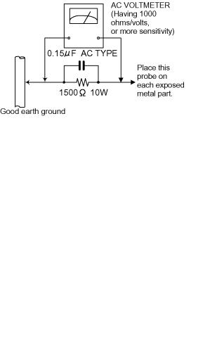
•Plug the AC line cord directly into the AC outlet. Using a "Leakage Current Tester", measure the leakage current from each exposed metal parts of the cabinet, particularly any exposed metal part having a return path to the chassis, to a known good earth ground. Any leakage current must not exceed 0.5mA AC (r.m.s.).
•Alternate check method
Plug the AC line cord directly into the AC outlet. Use an AC voltmeter having, 1,000 ohms per volt or more sensitivity in the following manner. Connect a 1,500 ohm 10W resistor paralleled by a 0.15 µF AC-type capacitor between an
exposed metal part and a known good earth ground. Measure the AC voltage across the resistor with the AC voltmeter.
Move the resistor connection to each exposed metal part, particularly any exposed metal part having a return path to the chassis, and measure the AC voltage across the resistor. Now, reverse the plug in the AC outlet and repeat each measurement. Voltage measured any must not exceed 0.75 V AC (r.m.s.). This corresponds to 0.5 mA AC (r.m.s.).
1.2Warning
(1)This equipment has been designed and manufactured to meet international safety standards.
(2)It is the legal responsibility of the repairer to ensure that these safety standards are maintained.
(3)Repairs must be made in accordance with the relevant safety standards.
(4)It is essential that safety critical components are replaced by approved parts.
(5)If mains voltage selector is provided, check setting for local voltage.
1.3Caution
Burrs formed during molding may be left over on some parts of the chassis.
Therefore, pay attention to such burrs in the case of preforming repair of this system.
1.4 Critical parts for safety
In regard with component parts appearing on the silk-screen printed side (parts side) of the PWB diagrams, the parts that are printed over with black such as the resistor (  ), diode (
  ) and ICP (
  ) or identified by the "
 " mark nearby are critical for safety.
When replacing them, be sure to use the parts of the same type and rating as specified by the manufacturer. (Except the JC version)
(No.A0041)1-3

XV-N50BK,XV-N55SL
1.5 Preventing static electricity
Electrostatic discharge (ESD), which occurs when static electricity stored in the body, fabric, etc. is discharged, can destroy the laser diode in the traverse unit (optical pickup). Take care to prevent this when performing repairs.
1.5.1Grounding to prevent damage by static electricity
Static electricity in the work area can destroy the optical pickup (laser diode) in devices such as DVD players. Be careful to use proper grounding in the area where repairs are being performed.
(1)Ground the workbench
Ground the workbench by laying conductive material (such as a conductive sheet) or an iron plate over it before placing the traverse unit (optical pickup) on it.
(2)Ground yourself
Use an anti-static wrist strap to release any static electricity built up in your body.
(3)Handling the optical pickup
•In order to maintain quality during transport and before installation, both sides of the laser diode on the replacement optical pickup are shorted. After replacement, return the shorted parts to their original condition.
(Refer to the text.)
•Do not use a tester to check the condition of the laser diode in the optical pickup. The tester's internal power source can easily destroy the laser diode.
1.6Handling the traverse unit (optical pickup)
(1)Do not subject the traverse unit (optical pickup) to strong shocks, as it is a sensitive, complex unit.
(2)Cut off the shorted part of the flexible cable using nippers, etc. after replacing the optical pickup. For specific details, refer to the
replacement procedure in the text. Remove the anti-static pin when replacing the traverse unit. Be careful not to take too long a time when attaching it to the connector.
(3)Handle the flexible cable carefully as it may break when subjected to strong force.
(4)I t is not possible to adjust the semi-fixed resistor that adjusts the laser power. Do not turn it.
1-4 (No.A0041)

1.7 Importance admistering point on the safety
|
|
|
P901 |
|
|
|
|
|
|
B4 |
EP951 |
|
C904 |
C905 |
R901 |
C908 |
|
|
|
B402 |
C907 |
|||||
|
|
|
|
R910 |
|
|
|
|
|
|
|
|
|
B104 |
|
|
|
|
|
|
|
C918 |
D901 |
D903 |
|
|
|
|
|
|
|
D902 |
|
||
|
|
|
|
|
|
|
||
|
C951 |
|
FC901 |
|
|
|
|
|
|
D960 |
|
|
IC901 |
|
C913 |
||
CN901 |
C802C808 |
FC902 |
L901 |
R913 |
R906 |
|||
R951 |
R912 |
|||||||
|
|
|
|
|
|
C914 |
||
|
|
|
|
|
|
|
D904 |
|
|
|
|
|
C902 |
R915 |
|
R903 |
|
|
|
Q951 |
|
|
|
PC901 |
|
|
|
|
|
|
|
|
|
||
|
B110 |
|
|
|
|
|
|
|
|
B111 |
B202 |
|
|
|
|
|
|
|
|
|
|
|
|
|
||
|
B112 |
|
|
|
|
|
|
|
|
|
|
|
|
|
B8 |
|
|
|
|
|
|
|
|
B9 |
|
|
|
|
B16 |
|
|
B109 |
|
||
|
|
|
|
|
|
|||
|
|
B17 |
|
|
|
|
|
|
|
|
B18 |
|
|
|
|
|
|
|
|
|
|
|
|
|
B803 |
|
|
|
|
|
|
|
B10 |
B401 |
|
|
|
|
|
|
|
B11 |
|
|
B129 |
C701 |
B128 |
|
EP952 |
|
XV-N50BK,XV-N55SL
L953
|
|
B19 |
C963 |
|
C965 |
|
|
|
|
|
|
B6 |
D956 |
|
C966 |
|
|
|
|
|
|
|
|
C964 |
L954 |
|
C988 |
|
|
|
|
|
|
|
C967 |
L955 |
B207 |
|
|
|
|
|
|
D957 |
D954 |
|
|
|
J702 |
|
|
|
|
|
D955 |
|
|
B404 |
|
|
|
|
|
|
C958 |
|
|
|
L709 |
|
|
|
|
|
|
L952 |
|
|
|
|
|
|
|
D953 |
|
L951 |
|
|
|
|
|
|
|
|
|
|
|
B601 |
L710 |
|
|
|
|
|
|
|
|
|
|
|
|
|
|
|
|
|
|
B603 |
|
|
|
|
|
T901 |
C952 |
|
|
|
S902 |
|
|
|
|
|
|
|
|
||
|
|
D951 |
|
|
C953 |
C955 |
|
|
|
C906 |
|
|
|
|
|
|
|
||
|
|
|
|
R954 |
|
|
|
|
|
|
|
|
C950 |
D952 |
|
C959 |
B604 |
B3 |
|
|
|
|
CP951 |
|
|
||||
|
|
|
|
|
|
|
|
|
S901 |
|
IC952 |
|
|
|
|
|
|
|
|
|
|
|
|
|
B301 |
|
|
|
|
|
|
|
|
|
B107 |
|
|
|
|
|
|
|
|
|
B101 |
|
|
C762 |
|
|
|
|
C970 |
|
B403 |
|
|
|
|
|
|
|
|
|
|
|
Q754 |
||
|
|
|
|
|
|
B801 |
|
|
|
|
|
|
|
|
|
|
|
|
|
|
|
|
|
|
|
B802 |
|
B201 |
|
|
|
|
|
|
|
B901 |
|
C761 |
Q753 |
|
|
|
|
|
|
B804 |
|
|
|
B102 |
|
|
|
B106 |
|
B902 |
|
|
|
|
|
|
|
|
|
|
|
||
B7 |
|
|
|
|
|
|
|
|
J603 |
B103 |
B501 |
B206 |
|
|
|
|
|
|
|
|
|
|
|
CN904 |
|
|
|
|
|
|
|
|
|
|
|
|
|
CN651 |
|
|
|
|
|
|
WC802 |
|
|
|
|
|
|
|
|
|
B108 |
|
|
|
|
|
|
|
|
|
|
B203 |
|
|
WC801 |
|
|
|
|
|
|
|
|
|
|
|
|
|
|
|
EP953 |
C957 |
|
B602 |
|
|
|
|
|
|
Q953 |
|
C973 |
|
|
|
|
|
|
|
B55 |
|
|
|
EP910 |
|
|
|
|
|
|
CN902 |
|
CN903 |
|
|
|
|
|
|
R966 |
|
|
|
|
|
|
|
|
|
|
|
B1 |
B2 |
|
Full Fuse Replacement Marking
Graphic symbol mark
(This symbol means fast blow type fuse.)
should be read as follows ;
FUSE CAUTION
FOR CONTINUED PROTECTION AGAINST RISK OF FIRE, REPLACE ONLY WITH SAME TYPE AND RATING OF FUSES ;
F901 : 1.6 A / 125 V
Marquage Pour Le Remplacement
Complet De Fusible
Le symbole graphique (Ce symbole signifie fusible de type a fusion rapide.)
doit etre interprete comme suit ;
PRECAUTIONS SUR LES FUSIBLES
POUR UNE PROTECTION CONTINUE CONTRE DES RISQUES D'INCENDIE, REMPLACER SEULEMENT PAR UN FUSIBLE DU MEME TYPE ;
F901 : 1.6 A / 125 V
(No.A0041)1-5
XV-N50BK,XV-N55SL
1.8Important for laser products
(1)CLASS 1 LASER PRODUCT
(2)DANGER : Invisible laser radiation when open and inter lock failed or defeated. Avoid direct exposure to beam.
(3)CAUTION : There are no serviceable parts inside the Laser Unit. Do not disassemble the Laser Unit. Replace the complete Laser Unit if it malfunctions.
(4)CAUTION : The compact disc player uses invisible laser radiation and is equipped with safety switches which prevent emission of radiation when the drawer is open and the safety interlocks have failed or are de feated.
It is dangerous to defeat the safety switches.
(5)CAUTION : If safety switches malfunction, the laser is able to function.
(6)CAUTION : Use of controls, adjustments or performance of procedures other than those specified herein may result in hazardous radiation exposure.
 CAUTION
Please use enough caution not to see the beam directly or touch it in case of an adjustment or operation check.
VARNING
Osynlig laserstrålning är denna del är öppnad och spårren är urkopplad. Betrakta ej strålen.
VARO
Avattaessa ja suojalukitus ohitettaessa olet alttiina näkymättömälle lasersäteilylle. Älä katso säteeseen.
ADVARSEL
Usynlig laserstråling ved åbning, når sikkerhedsafbrydere er ude af funktion. Undgå udsasttelse for stråling.
ADVARSEL
Usynlig laserstråling ved åpning, når sikkerhetsbryteren er avslott. unngå utsettelse for stråling.
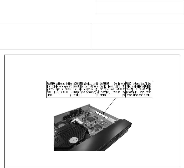
REPRODUCTION AND POSITION OF LABEL and PRINT
WARNING LABEL and PRINT
The inside of a chassis base
TOAVBinEOtreAIaDrMdCloDia.AckIRtUiofTEanIilCOeTdwNEho:eXrndPIneOvfoeSispa(Ueiebte)RnldeE.alandssetruårrleköpnos.pptnprVåalaAlnddRin.NgoINcnBhGäer:trsdapOekärsntaynr(neas)lingdeejällarästeerrlsa-efsfikfouskrntersAkålinrtrthDioåeVnlingdA.sgRaUvSfbenErddyLgd:åeåreUbusndye(insdnrgæt)lig,u-dlaensårseätrla-eseaeslterjatseiinluVätenkAa.ituilRyOslle:n.oAähvkitÄayetlmätttaäaeetstksösasamtasäojalloesleuto-
(f)
1-6 (No.A0041)
XV-N50BK,XV-N55SL
1.9 Precautions for Service
1.9.1 Handling of Traverse Unit and Laser Pickup
(1)Do not touch any peripheral element of the pickup or the actuator.
(2)The traverse unit and the pickup are precision devices and therefore must not be subjected to strong shock.
(3)Do not use a tester to examine the laser diode. (The diode can easily be destroyed by the internal power supply of the tester.)
(4)To replace the traverse unit, pull out the metal short pin for protection from charging.
(5)When replacing the pickup, after mounting a new pickup, remove the solder on the short land which is provided at the center of the flexible wire to open the circuit.
(6)Half-fixed resistors for laser power adjustment are adjusted in pairs at shipment to match the characteristics of the optical block. Do not change the setting of these half-fixed resistors for laser power adjustment.
1.9.2 Destruction of Traverse Unit and Laser Pickup by Static Electricity
Laser diodes are easily destroyed by static electricity charged on clothing
or the human body. Before repairing peripheral elements of the traverse unit or pickup, be sure to take the following electrostatic protection:
(1)Wear an antistatic wrist wrap.
(2)With a conductive sheet or a steel plate on the workbench on which the traverse unit or the pick up is to be repaired, ground the sheet or the plate.
(3)Please be sure to make the switch of a relay board into the "SHORT" side before drawing out a wire from the connector CN101 on a servo control board,
when taking out a mechanism assembly from a main body.
And please be sure to make a switch into the "OPEN" side after connecting a wire to CN101, when it mounts a mechanism assembly in a main body.
(4)After removing the flexible wire from the connector (CN1), short-circuit the flexible wire by the metal clip.
(5)Short-circuit the laser diode by soldering the land which is provided at the center of the flexible wire for the pickup. After completing the repair, remove the solder to open the circuit.
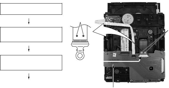
The procedure for protecting a pickup
The switch on a relay board is changed from "OPEN" to "SHORT."
A wire is extracted from the connector CN101 on a servo control board.
It solders to the short circuit part on a flexible wire, and it is made to shortcircuit.
Short circuit
Short circuit
CN1
A flexible wire is extracted from the |
|
Relay board |
connector CN1 on a relay board. |
|
|
|
|
|
|
|
|
In case you assemble, please do all work conversely. |
|
|
(No.A0041)1-7
XV-N50BK,XV-N55SL
SECTION 2
Disassembly method
2.1 Main body section
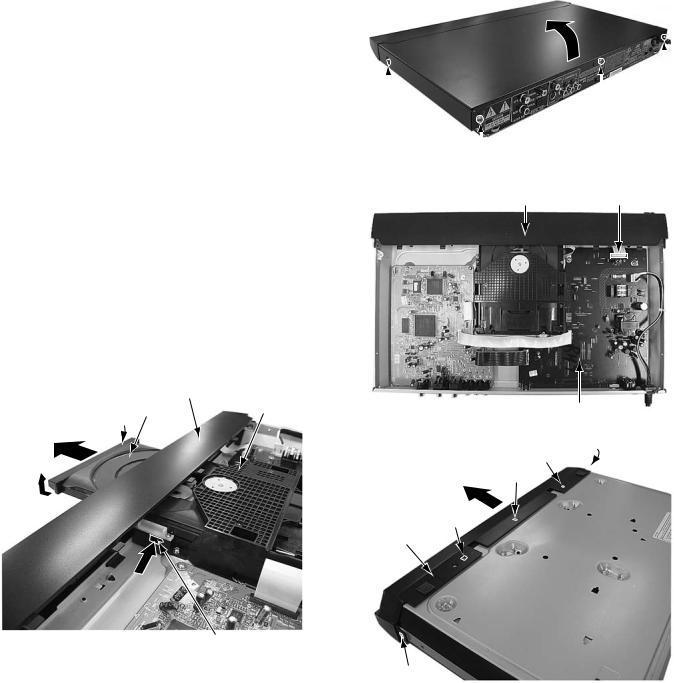
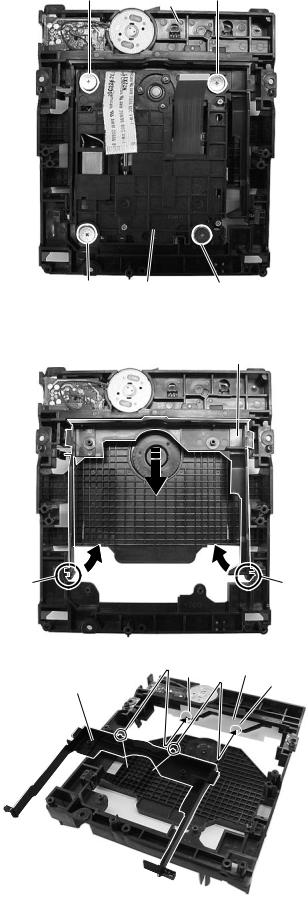
2.1.1 Removing the top cover (See Figure 1)
(1)Remove the two screws A attaching the top cover on both sides of the main body.
(2)Remove the three screws B attaching the top cover on the
back of the main body. |
|
TOP COVER |
|
|
|
|
|
(3) Raise the both sides and lower part of the rear of the top |
|
|
|
|
B |
||
cover, with opening them slightly in an outward direction. |
A |
|
|
|
|
|
|
|
|
|
|
|
|
||
And the top cover will be removed. |
x 2 |
|
|
|
|
||
|
|
|
|
B |
|||
|
|
|
|
|
|
|
|
|
|
|
|
|
|
|
|
|
|
B |
|
|
|
|
|
|
|
|
Fig.1 |
|
|
|
|
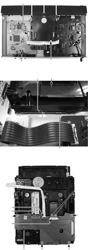
2.1.2 Removing the front panel assembly (See Figure 2, Figure 3, Figure 4) |
|
|
|
|
|||
• Prior to performing the following procedure, remove the top |
|
Front panel assembly |
CN901 |
||||
cover. |
|
||||||
|
|
|
|
|
|
|
|
•There is no need to remove the mechanism assembly.
(1)Insert a kind of screwdriver in a hole located in the right
side of mechanism assembly, and push a lever until it cannot be inserted any further.
(2)And then, a tray will come out. Remove the tray in an upper direction, with slightly opening the lower part of fitting in an outward direction.
(3)Disconnect the card wire from connector CN901 on the power supply board.
(4)Hook a and b are removed respectively, and the front panel
assembly is removed.
|
Front panel assembly |
|
FittingTray |
Mechanism assembly |
Power supply board |
|
||
|
Fig.3 |
|
|
|
Hook a |
|
|
Hook b |
|
|
Hook b |
|
Front panel |
Hook b |
|
assembly |
|
Push |
|
|
Hole and lever
Fig.2
Hook a
Fig.4
1-8 (No.A0041)
XV-N50BK,XV-N55SL
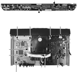
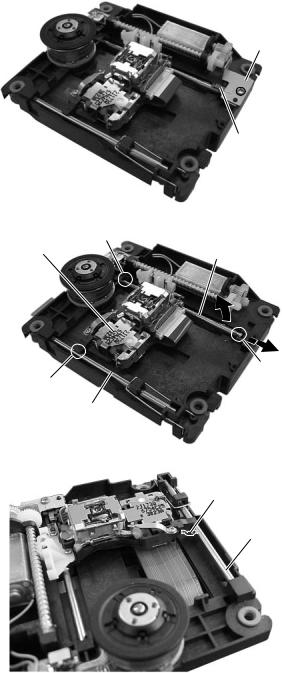
2.1.3 Removing the mechanism assembly (See Figure 2, Figure 5, Figure 6)
•Prior to performing the following procedure, remove the top cover.
•There is no need to remove the front panel assembly.
(1)Insert a kind of screwdriver in a hole located in the right side of mechanism assembly, and push a lever until it cannot be inserted any further. (See Figure 2)
(2)And then, a tray will come out. Remove the tray in an upper direction, with slightly opening the lower part of fitting in an outward direction. (See Figure 2)
(3)Remove the three screws C attaching the mechanism assembly.
(4)The switch on a relay board is made into the “SHORT” side.
(5)Disconnect the card wire from connector CN101 on the servo control and signal output terminal board.
(6)Remove the mechanism assembly by lifting the rear part of the mechanism assembly.
Mechanism assembly
CN101 C |
C |
||
|
|
|
|
|
|
|
|
ATTENTION:
Please be sure to make the switch on a relay board into a “SHORT” side before disconnect a card wire from the connector CN101 on servo control and signal output terminal board. Moreover, please be sure to make a switch into the “OPEN” side after inserting a card wire in a connector CN101 at the time of an assembly.
There is a possiblity of destroying the laser diode of a pick-up unit with static electricity.
2.1.4 Removing the relay board (See Figure 7)
•Prior to performing the following procedure, remove the mechanism assembly.
(1)Remove the four screws D attaching the relay board.
(2)Disconnect the card wire from connector CN2,CN3 on the relay board respectively.
(3)Disconnect the flexible wire from connector CN1 on the relay board from pick-up unit.
ATTENTION:
At this time, please extract the wire after short-circuited of two places on the wire in part c with solder. Please remove the solder two places of part c after connecting the wire with CN1 when reassembling.
There is a possibility of destroying the laser diode of a pick-up unit with static electricity.
Servo control and signal |
C |
|
|
output terminal board |
|
Fig.5
Switch |
Mechanism assembly |
SHORT
 OPEN
OPEN
Relay board
Fig.6
Part c
CN2 |
|
CN3 |
|
D |
D |
CN1 |
|
Relay board D |
D |
Fig.7
(No.A0041)1-9
XV-N50BK,XV-N55SL
2.1.5 Removing the rear panel (See Figure 8, Figure 9)
•Prior to performing the following procedure, remove the top cover.
(1)Remove the eight screws E attaching the rear panel.
(2)Disconnect the power cord from connector P901 on the power supply board
(3)Remove tie band.
Rear panel
|
|
|
|
|
|
|
|
|
|
|
|
|
|
|
|
|
|
|
|
|
|
|
|
E |
|
|
|
E |
|
E |
|||||
|
|
|
|
|
Fig.8 |
|
|
|
|||
|
F |
|
|
|
F |
G |
CN901 |
||||
|
|
|
|
|
|
|
|
|
|
|
G |
|
|
|
|
|
|
|
|
|
|
|
P901 |
CN101 |
|
|
|
|
|
|
|
|
|
|
|
CN502 |
|
|
|
|
|
|
|
|
|
|
|
|
|
|
CN902,CN903 G |
Power supply board |
|||||||
Servo control and signal |
|
|
|
||||||||
output terminal board
Fig.9
2.1.6Removing the servo control and signal output terminal board. (See Figure 9)
• Prior to performing the following procedure, remove the top cover/rear panel.
(1) Remove the two screws F attaching the servo control and signal output terminal board.
(2) Disconnect the card wire from connector CN101,CN502 on the servo control and signal output terminal board.
(3) Disconnect the flat wire from connector CN902,CN903 on the power supply board.
2.1.7Removing the power supply board. (See Figure 9)
•Prior to performing the following procedure, remove the top cover/rear panel.
(1)Remove the three screws G attaching the power supply board.
(2)Disconnect the wire from connector CN901,CN902, CN903,CN904 on the power supply board.
(3)Disconnect the socket wire from socket P901 on the power supply board.
1-10 (No.A0041)
|
|
XV-N50BK,XV-N55SL |
2.2 Loading mechanism assembly |
|
|
2.2.1 Removing the tray (See Figure 1, Figure 2, Figure 3, Figure 4, Figure 5, Figure 6) |
|
|
(1) |
Push a of the slide cam on the hole in the right side of the |
Tray |
|
loading base by using a driver until it stops. (See Figure 1.) |
|
|
|
|
(2) |
The tray comes out. Pull the tray in a front direction until it |
|
|
stops. |
|
(3) |
Remove the two screws A attaching the slide bracket. (See |
|
|
Figure 2.) |
|
(4) |
Tilt the tray in a direction of the arrow around the point in |
|
|
the left rear part of the tray. (See Figure 3.) |
|
(5) |
The rail of the tray is removed from b of the loading base. |
|
|
Then, remove the tray upward. (See Figure 4.) |
|
Attaching the tray:
Engage c of the loading base to the projection of the tray while tilting the tray to the left. Turn the tray in a direction of the arrow, and attach the slide bracket. (See Figure 5.)
Note: |
The point in the left rear part |
|
Fig.3 |
||
Prior to the procedure above, move the slide cam in a direction |
||
|
||
of the arrow so that d of the slide cam can be inserted in e of |
|
|
the tray. (See Figure 6.) |
|
|
Tray |
|
|
Loading base part b |
|
Rail of the tray |
|
Fig.4 |
Push |
|
Slide cam part a |
Loading base |
Fig.1 |
|
A Slide bracketA |
Projection of the tray |
Tray |
Loading base part c
Fig.5
Fig.2
Part e
 Part d
Slide cam
Fig.6
(No.A0041)1-11
XV-N50BK,XV-N55SL
2.2.2 Removing the traverse mechanism assembly (See Figure 7)
Reverse the loading mechanism assembly. Remove the four screws B attaching the traverse mechanism assembly. Remove the traverse mechanism assembly upward.
2.2.3 Removing the elevator (See Figure 8 and Figure 9)
•Prior to the following procedure, remove the traverse mechanism assembly.
(1)Remove the two arms of the elevator from the two parts f by moving the arms in a direction of the arrow.
(2)Pull out the elevator in a rear direction.
Attaching the elevator:
Engage the two holes g to the two shafts on the front part of the elevator. And then, attach the elevator.
Part f
1-12 (No.A0041)
Loading mechanism
B assembly B
B Traverse mechanism B
assembly
Fig.7
Elevator
Part f
Fig.8
g Slide cam
g
Elevator
Shaft
Fig.9
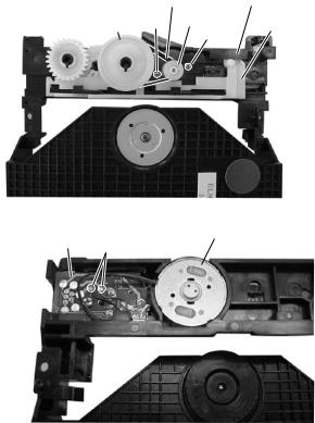
2.2.4 Removing the loading motor (See Figure 10 and Figure 11)
•Prior to the following procedure, remove the tray, the traverse mechanism assembly, and the elevator.
(1)Remove the belt from the pulley.
(2)Remove two screws C attaching the loading motor.
(3)Remove two solders h on the switch board.
XV-N50BK,XV-N55SL
|
Belt |
Loading base |
|
|
|
Pulley |
C Pulley |
Slide cam |
|
C |
|
Fig.10
Loading motor
Switch board Part h
Fig.11
(No.A0041)1-13
XV-N50BK,XV-N55SL
2.3 Traverse mechanism assembly
2.3.1 Removing the pickup (See Figure 12, Figure 13, and Figure 14)
•Prior to the following procedure, remove the traverse mechanism assembly.
(1) |
Remove one screw D attaching the plate. |
|
(2) |
Remove the plate and the leaf spring. |
Plate |
(3)Lift i of the shaft 1, and pull out the shaft 1 from j.
(4)Remove k of the pickup from the shaft 2.
Attaching the pickup:
(1)Engage k of the pickup to the shaft 2.
Note:
As Figure 14 shows, the spring must come under the shaft 2.
(2)Insert the shaft 1 in j, and attach the shaft 1 to i.
(3)Attach the leaf spring, and then attach the plate. Fix the leaf spring and the plate by using the screw D.
 D
D
Leaf spring
Fig.12
Part j
Pick-up
Shaft 1
Part i
Part k
Shaft 2
Fig.13
Spring
Shaft 2
Fig.14
1-14 (No.A0041)
XV-N50BK,XV-N55SL
SECTION 3
Adjustment
3.1Test mode setting method
(1)Unplug the power plug.
(2)Insert power plug into outlet while pressing both "PLAY" key and "STOP" key of the main body.
(3)The FL display shows " 0", and the main body turns to test mode. "
 " means the destination, and "0" means parameter adjustment status.
(4)To release test mode, press "POWER" key of the main body.
NOTE:
Each pressing of "CHOICE" key of the remote controller in test mode changes the mode as follows.
|
|
|
|
------------------------------0 |
|
Becames test mode |
|
|
|
|
|
_ |
_ ------------- |
Version of firmware |
|
|
|
||
FL Display becames all lighting |
|||
|
|
|
|
CHECK ------------------------- |
|
Check mode |
|
|
|
|
|
|
|
|
|
EXPERT |
----------------------- |
Not used |
|
|
|
|
|
|
|
|
|
3.2Method of displaying version of firmware
(1)Set the main body at test mode.
(2)Press "CHOICE" key of the remote controller once. Then, version number and alphabetical letter of the system controller and the back end are displayed in the FL display as follows:
FL Display (Example)
System controller
 04_02_17
  Back end
3.3 Initialization method
Please initialize according to the following procedures in the following case:
•Just after you upgrade the firmware.
•After you confirm the symptoms that a customer points out. First Initialize, and then confirm whether the symptoms are improved or not.
•After servicing, before returning the main body to a customer. (Initialized main body should be returned to a customer.)
(1)Set the main body at test mode.
(2)Press "PAUSE" key of the main body.
(3)When initialization is completed, the FL display changes from " 0" to "
 00" and a progressive indicator lights up. (The left "0" of "00" is not always "0". It shows parameter adjustment status.)
|
|
|
TV |
DVD |
OPEN/ |
|
STANDBY/ON |
||
CLOSE |
|
TV |
DVD |
|
TV1 |
TV2 |
|
TV3 |
|
1 |
|
2 |
|
3 |
TV4 |
TV5 |
|
TV6 |
|
4 |
|
5 |
|
6 |
TV7 |
TV8 |
|
TV9 |
|
7 |
|
8 |
|
9 |
TV-/-- |
TV0 |
|
MUTING |
|
10 |
0 |
|
+10 |
|
|
|
|
TITLE/ |
TV/VIDEO |
RETURN |
|
GROUP |
CANCEL |
|
|
U |
CH |
|
ME |
EN |
|
|||
PM |
|
+ |
|
NU |
TO |
|
|
|
|
VOL |
|
|
|
VOL+ |
|
|
ENTER |
|
|
CH |
|
CH |
|
EEN |
OIC |
E |
|
|
CR |
|
|
|
ONS |
|
PREVIOUS |
|
NEXT |
||
CLEAR |
SELECT |
|
||
SLOW- |
|
|
SLOW+ |
|
|
|
3D |
ZOOM |
VFP |
|
|
PHONIC |
||
|
|
|
|
PROGRESSIVE |
ANGLE |
SUB TITLE |
AUDIO |
SCAN |
|
|
||||
|
|
|
|
AMP |
REPEAT |
DIMMER |
VOL |
||
PLAY key (for test mode)
STOP key (for test mode)
CHOICE key |
POWER key FL Display |
(switch of mode) |
|
Progressive indicator |
PAUSE key |
|
(for initialize) |
||
(for initialize) |
||
|
(No.A0041)1-15
XV-N50BK,XV-N55SL
3.4 All-initialization method
Please perform all-initialization according to the following procedures in the following case:
•Just after you exchange the pick-up.
•Just after you exchange the spindle motor.
•Just after you exchange the traverse mechanism base.
NOTE:
Please perform all-initialization when you exchange the parts above and also when you remove the parts above.
•Just after the flap adjustment of the pick-up guide shaft
(1)Set the main body at test mode.
(2)Press and hold "BACKWARD SKIP" key of the main body for more than 2 seconds.
(3)When all-initialization is completed, the FL display changes from " 0" to "
 33".
33".
NOTE:
After all-initialization, be sure to perform optimization adjustment of Front End parameter.
3.5 Optimization adjustment of Front End parameter
Adjustment to optimize Front End parameter must be performed in each mechanism assembly of this model for high-speed starting. Please perform optimization according to the following procedures just after all-initialization is completed and when FL display shows anything except " 0" (For example when FL display shows "
 1", "
1", " 2", and "
 3") at test mode.
(1)Press "POWER" key of the main body to turn the main body on (not to set the main body at test mode).
(2)Insert the test disc VT-501 or commercial dual-layer DVD software.
(3)Remove the disc when the FL display changes from "READ" to disc information.
(4)Perform the same procedures as in (2) and (3) above by using the test disc CTS-1000 or commercial CD-DA software.
(5)Set the main body at test mode, and check that the FL display shows " 0".
0".
NOTE:
Status of this adjustment can be judged by the number displayed at test mode as follows:
DVD adjustment |
CD adjustment |
FL display at test mode |
|
|
|
Adjusted |
Adjusted |
0 |
|
|
|
Not adjusted |
Adjusted |
1 |
|
|
|
Adjusted |
Not adjusted |
2 |
|
|
|
Not adjusted |
Not adjusted |
3 |
|
|
|
NOTE:
As for a disc used for adjustment,
•Disc should be mounted. ("Mounting" means to display "READ" after the disc is inserted and then display the disc information.) Disc need not be played.
•If you do not have test disc either VT-501 (DVD) or CTS-1000 (CD-DA), use a commercial disc (for DVD, dual-layer software) after seeing and checking that the disc is neither curved nor foreseen that it may shake at the time of playback.
If you use a disc with bad features, starting time may be slow or disc may not be read.
|
|
|
TV |
DVD |
OPEN/ |
|
STANDBY/ON |
||
CLOSE |
|
TV |
DVD |
|
TV1 |
TV2 |
|
TV3 |
|
1 |
|
2 |
|
3 |
TV4 |
TV5 |
|
TV6 |
|
4 |
|
5 |
|
6 |
TV7 |
TV8 |
|
TV9 |
|
7 |
|
8 |
|
9 |
TV-/-- |
TV0 |
|
MUTING |
|
10 |
0 |
|
+10 |
|
|
|
|
TITLE/ |
TV/VIDEO |
RETURN |
|
GROUP |
CANCEL |
|
|
U |
CH |
|
ME |
EN |
|
|||
PM |
|
+ |
|
NU |
TO |
|
|
|
|
VOL |
|
|
|
VOL+ |
|
|
ENTER |
|
|
CH |
|
CH |
|
EEN |
OIC |
E |
|
|
CR |
|
|
|
ONS |
|
PREVIOUS |
|
NEXT |
||
CLEAR |
SELECT |
|
||
SLOW- |
|
|
SLOW+ |
|
|
|
3D |
|
|
|
|
PHONIC |
ZOOM |
VFP |
|
|
|
|
PROGRESSIVE |
ANGLE |
SUB TITLE |
AUDIO |
SCAN |
|
|
||||
|
|
|
|
AMP |
REPEAT |
DIMMER |
VOL |
||
PLAY key (for test mode)
STOP key (for test mode)
POWER key FL Display
BACKWARD SKIP key
(for All initialize : It pushes 2 seconds or more.)
1-16 (No.A0041)

XV-N50BK,XV-N55SL
3.6Display of current value of laser
(1)Set the main body at test mode.
(2)Press "CHOICE" key of the remote controller three times. Then, FL display is displayed "CHECK".
(3)The laser current value can be switched between the value of CD and that of DVD by pressing the following key of the remote controller.
FL Display (Example)
2530 0000 |
Remote controller "4" key --- Laser of CD |
|
Remote controller "5" key --- Laser of DVD |
The number shown in the FL display shows mA of current value of laser.
The first two numbers ("25" in "2530") shows current value of laser at the time of adjustment after the latest all-initialization, 25mA in this example.
The last two numbers ("30" in "2530") shows the present current value of laser, 30mA in this example.
The first two numbers ("25" in "2530") usually shows current value of laser at the time of shipment, so you can see how the product has been deteriorated by comparing the first two numbers ("25" in "2530") and the last two numbers ("30" in "2530").
CD:
The laser current value of 49 mA or less is normal.
The laser current value of over 50 mA is not normal. Laser diode of the pickup has been deteriorated.
DVD:
The laser current value of 64 mA or less is normal.
The laser current value of over 65 mA is not normal. Laser diode of the pickup has been deteriorated.
To return to test mode, press "STOP" key of the main body.
3.7 Flap adjustment of the pick-up guide shaft
Please perform flap adjustment of the pick-up guide shaft in the following case:
•Just after you exchange the pick-up.
•Just after you exchange the spindle motor.
•Just after you exchange the traverse mechanism base.
NOTE:
Please perform flap adjustment of the pick-up guide shaft when you exchange the parts above and also when you remove the parts above.
•When the reading accuracy of the signal is bad (There is a block noise in the screen, Screen stops in the outer circumference of a disc, etc.)
|
|
1 key (automatic adjustment) |
|
|||
|
|
|
|
|
5 key (laser of DVD) |
|
|
|
|
TV |
DVD |
|
|
OPEN/ |
|
STANDBY/ON |
|
|
||
CLOSE |
|
TV |
DVD |
|
|
|
TV1 |
TV2 |
|
TV3 |
|
|
|
1 |
|
2 |
|
3 |
6 key |
|
TV4 |
TV5 |
|
TV6 |
|
||
4 |
|
5 |
|
6 |
|
|
TV7 |
TV8 |
|
TV9 |
|
||
7 |
|
8 |
|
9 |
(display of jitter value) |
|
10 |
0 |
TITLE/ |
TV/VIDEO |
|
||
TV-/-- |
TV0 |
|
MUTING |
|
|
|
|
|
|
|
+10 |
|
|
RETURN |
|
GROUP |
CANCEL |
|
|
|
|
U |
CH |
|
ME |
|
|
EN |
|
|
|
|||
PM |
|
+ |
|
NU |
|
|
TO |
|
|
|
|
|
|
VOL |
|
|
|
VOL+ |
|
|
|
|
ENTER |
|
4 key (laser of CD) |
POWER key FL Display |
|
CH |
|
CH |
|
EEN |
||
OIC |
E |
|
|
CR |
|
|
|
|
|
ONS |
|
|
|
PREVIOUS |
|
NEXT |
|
|
||
CLEAR |
SELECT |
|
|
|
||
SLOW- |
|
|
SLOW+ |
CHOICE key |
|
|
|
|
3D |
|
PROGRESSIVE |
|
|
|
|
PHONIC |
ZOOM |
VFP |
|
|
ANGLE |
SUB TITLE |
AUDIO |
SCAN |
(switch of mode) |
|
|
|
|
|||||
REPEAT |
DIMMER |
VOL |
|
|||
|
|
|
|
AMP |
|
|
PLAY key
(for test mode and jitter value)
STOP key (for test mode)
(No.A0041)1-17
XV-N50BK,XV-N55SL
3.7.1 Tool for adjustment
*Stud: One set (four studs), Part number: JIGXVS40 (Note: One of the four studs is not used here.)
3.7.2 Preparation for adjustment
(1)See the disassembly procedure, and remove the Mechanism assembly from the main body.
(2)Remove the relay board attached to the mechanism assembly.
(If you disconnect the wires connected to the Relay board, connect them again.)
(3)Attach the three studs to the Mechanism assembly.
(4)Put the Mechanism assembly in the center of the main body, and connect the 50 pin wire from the connector CN4 on the Relay board to the connector CN101 on the Servo control & signal output terminal board.
Stud |
Mechanism |
Stud |
|
|
|
|
assembly |
Mechanism assembly |
|
|
|
|
|
CN4 |
|
|
CN101 |
|
|
Relay board |
Stud
CN4
Relay board
Servo contro & signal output terminal board
 Switch
OPEN 
 SHORT
SHORT
3.7.3 Adjustment
(1)Set the unit to test mode.
(2)Press the "CHOICE" key of the remote controller three times, and the FL display is displayed "CHECK".
(3)Insert a test disc (VT-501), and press the numeric key "1" of the remote controller for automatic adjustment.
(4)After a few seconds, press the numeric key "6" of the remote controller. Then, the FL display displays a jitter value.
(5)Turn the adjustment screws on the underside of the traverse mechanism with phillips screw driver until the maximum jitter value is displayed on the FL display. (In this model, a bigger jitter value means a better result.)
NOTE:
During operation, the switch on the Relay board should be switched to "OPEN".
Reference values to judge whether the jitter is allowable or not are displayed, instead of actual jitter values.
Screw a
 Screw b
POINT:
Turn the adjustment screws a and b to the same angle in the right direction. And turn the adjustment screws a and b to the same angle in the left direction. Then, turn the screws a and b in either the right or the left direction to increase the number of jitter. Don't turn the adjustment screw c.
 Screw c
1-18 (No.A0041)
XV-N50BK,XV-N55SL
3.8 Upgrading of firmware
The latest firmware for upgrading is updated in "Optical disc CSG" page in JS-net.
At the time of service, compare the version of the product and the latest version, and upgrade the old version into the latest version.
(1)Press "POWER" key of the main body to turn the main body on
(2)Insert the upgrade disc.
(3)When FL display of the main body changes from "READ" to "UP", press "cursor UP" key ( ) of the remote controller.
(4)The entire screen becomes blue, and upgrading starts.
(5)The tray opens automatically. Remove the upgrade disc.
(6)The screen returns to the normal screen. Then, press "POWER" key of the main body. When the stand-by indicator is lighted, upgrading is completed.
(7)Set the main body at test mode, and perform initialization. Then, confirm the version of the firmware.
Firmware upgrade Disc ... press UP
Upgrade application initializing...
|
|
|
|
|
NO DISC |
After inserting the up-grade disc |
While upgrading (blue screen) |
When up-grade is completed |
|||
|
TV |
DVD |
UP key |
|
PLAY key |
CLOSE |
TV |
DVD |
|
||
OPEN/ |
STANDBY/ON |
(for firmware upgrade) |
|
(for test mode) |
|
1 |
2 |
3 |
|
||
TV1 |
TV2 |
TV3 |
|
|
|
TV4 |
TV5 |
|
TV6 |
|
4 |
|
5 |
|
6 |
TV7 |
TV8 |
|
TV9 |
|
7 |
|
8 |
|
9 |
TV-/-- |
TV0 |
|
MUTING |
|
10 |
0 |
|
+10 |
|
|
|
|
TITLE/ |
TV/VIDEO |
RETURN |
|
GROUP |
CANCEL |
|
|
U |
CH |
|
ME |
EN |
|
|||
PM |
|
+ |
|
NU |
TO |
|
|
|
|
VOL |
|
|
|
VOL+ |
|
|
ENTER |
|
|
CH |
|
CH |
|
EEN |
OIC |
E |
|
|
CR |
|
|
|
ONS |
|
PREVIOUS |
|
NEXT |
||
CLEAR |
SELECT |
|
||
SLOW- |
|
|
SLOW+ |
|
|
|
3D |
ZOOM |
VFP |
|
|
PHONIC |
||
|
|
|
|
PROGRESSIVE |
ANGLE |
SUB TITLE |
AUDIO |
SCAN |
|
|
||||
|
|
|
|
AMP |
REPEAT |
DIMMER |
VOL |
||
STOP key (for test mode)
CHOICE key |
POWER key FL Display |
OPEN/CLOSE key |
|
||
(switch of mode) |
|
|
Progressive indicator |
PAUSE key |
|
(for initialize) |
||
(for initialize) |
||
|
(No.A0041)1-19

XV-N50BK,XV-N55SL
3.9Attention when pick-up is exchanged
(1)Flexible wire, pick-up spring, switch actuator, and lead spring are removed from an old pick-up (broken the one).
Guide:
Flexible wire, pick-up spring and switch actuator,lead spring are removed without each decomposing while assembled.
(2)The above-mentioned parts are installed in a new pick-up (non-defective article).
(3)A flexible wire is inserted in the connector which has taken side with the pick-up, and solder is put up to short land part "a" two places on a flexible wire.
(4)The electrostatic breakdown protection circuit attached to the pick-up is cut.
ATTENTION:
Please cut the electrostatic breakdown protection circuit attached to the pick-up after solder is put up to two places on a flexible wire short land part "a" of the insertion of a flexible wire this time in the connector without fail.
The procedure might be mistaken and if solder has not surely adhered to two places on a flexible wire short land part "a", the laser diode in the pick-up be destroyed again.
(5)The pick-up is installed in the traverse mechanism.
(6)A flexible wire is connected with connector CN101 on the servo control board by installing the traverse mechanism in the loading mechanism.
(7)Solder in two places on a flexible wire in part "a" is removed.
ATTENTION :
Please remove solder in two places in part "a" after connecting a flexible wire with connector CN1 on the relayl board without fail this time.
When the procedure is mistaken, the laser diode in the pick-up might be destroyed.
Please remove solder in two places in part "a" surely.
1-20 (No.A0041)
 Switch actuator
 Lead spring
Pick-up
Pick-up spring 
Flexible wire
Electrostatic breakdown protection circuit
Electrostatic breakdown protection circuit
CN1
Flexible wire
 Connector
Short land  part "a"

 Cutting part
Short land part "a"
Relay board
XV-N50BK,XV-N55SL
3.10 Confirm method of operation
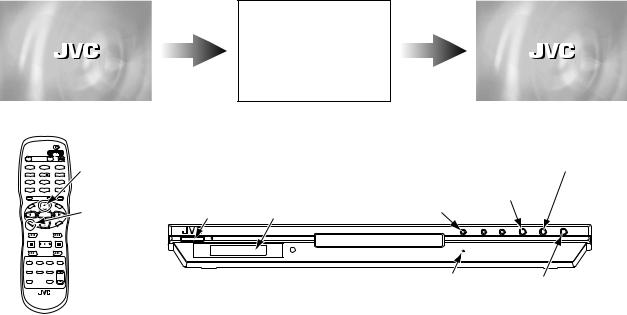
Please confirm the operation of the undermentioned item after doing the repair and the upgrade of the firmware.
Initialize |
Refer to the initialization method. |
All-initialize |
Refer to the All-initialization method. |
Parameter adjustment status |
Set the main body at test mode, and check that the FL display shows " 0". |
Opening picture check (Power ON) |
It should be display "JVC" |
Muting working |
The noise must not be had to the performance beginning when you push "PLAY" button or |
|
at ON/STANDBY. |
FL Display |
The mark and the logo, etc. displayed by each operation must be displayed correctly. |
|
FL Display should light correctly without any unevenness. |
All Function button |
All function buttons should worked correctly with moderate click feeling. |
Open and close movement of tray |
When press OPEN/CLOSE button the tray should move smoothly without any noise. |
Remote controller unit working |
Check the correctly operation in use of remote controller unit. |
Reading of TOC |
Be not long in the malfunction. |
Search |
Both forward-searches and backward-searches should be able to be done. |
|
Do not stop be searching or after the search. |
Skip |
Both forward-skip and backward-skip should be able to be done. |
|
Do not stop be after the skip. |
Playback |
Do not find abnormality etc. of tone quality and the picture quality. |
Most outside TITLE playback check |
Play VT-501 TITLE 59 CHAPTER 1 , check normal playback. |
(No.A0041)1-21
XV-N50BK,XV-N55SL
3.11Troubleshooting 3.11.1 Servo volume
Press OPEN /CLOSE key
Is tray |
N |
Confirmation of tray drive circuit |
|
operation |
|||
|
and circuit in surrounding |
||
correct? |
|
||
|
|
Y
Is the traverse moving |
N |
along the innermost |
|
perimeter for SW detection? |
|
Y |
|
"NO DISC" message appears Y immediately after vertical movement of the pick-up lens
N
See "(3) Traverse movement error" in "Check points for individual errors"
See "(2) Disk detection, distinction error" in "Check points for individual errors"
The state that DISC does not rotate continues for several seconds, and becomes NO DISC or an error display afterwards.
The rotation of DISC becomes high-speed and abnormal, and becomes NO DISC or an error display afterwards.
Y See "(1) Spindle startup error"
 in "Check points for individual errors"
N
Is focus retraction OK? |
|
|
|
|
|
|
|
|
|
|||||||||
|
|
|
|
|
|
|
|
|
||||||||||
FE |
|
|
|
|
|
|
|
|
|
|
|
|
|
|||||
|
|
|
|
|
|
|
|
|
N |
|
See "(4) Focus ON error" |
|
||||||
|
OFF |
|
ON |
|
|
|
|
|
|
in "Check points for |
|
|||||||
|
|
|
|
|
|
|
|
|||||||||||
Even when it retracts |
|
|
|
|
|
|
individual errors" |
|
||||||||||
correctly, if it is out of focus |
|
|
|
|
|
|
|
|||||||||||
and makes repeated retries |
|
|
|
|
|
|
|
|
|
|||||||||
with a clicking sound, it is |
|
|
|
|
|
|
|
|
|
|||||||||
in error. |
|
|
|
|
|
|
|
|
|
|
|
|
|
|
||||
|
|
|
|
|
|
|
|
Y |
|
|
|
|
|
|
|
|
|
|
|
|
|
|
|
|
|
|
|
|
|
|
|
|
|
|
|
||
Is tracking retraction OK? |
|
|
|
|
|
|
|
|
||||||||||
TE |
|
|
|
|
|
|
|
|
|
|
|
|
|
|
|
|||
|
|
|
|
|
|
|
|
|
|
|
N |
|
|
See "(5) Tracking ON error" |
|
|||
|
|
|
|
|
|
|
|
|
|
|||||||||
|
|
|
|
|
|
|
|
|
|
|
|
|
|
|
|
|
in "Check points for |
|
|
OFF |
|
ON |
|
|
|
|
|
||||||||||
|
|
|
|
|
|
|
|
individual errors" |
|
|||||||||
|
|
|
|
|
|
|
|
|
||||||||||
If TE waveform reappears |
|
|
|
|
|
|
|
|||||||||||
|
|
|
|
|
|
|
|
|||||||||||
or fails to converge after the |
|
|
|
|
|
|
|
|
||||||||||
TE retraction, it is in error. |
|
|
|
|
|
|
|
|
||||||||||
|
|
|
|
|
|
|
|
Y |
|
|
|
|
|
|
|
|
||
|
|
|
|
|
|
|
|
|
|
|
|
|
|
|
|
|||
Is the spindle servo |
|
|
|
|
|
|
|
|
||||||||||
|
|
|
|
|
|
See "(6) Spindle CLV error" |
|
|||||||||||
locked correctly? |
|
N |
|
|
|
|||||||||||||
Is the RF OUT waveform |
|
|
|
|
|
|
in "Check points for |
|
||||||||||
|
|
|
|
|
||||||||||||||
|
|
|
|
|
|
individual errors" |
|
|||||||||||
|
locked correctly? |
|
|
|
|
|
|
|
|
|||||||||
|
|
|
|
|
|
|
|
|
||||||||||
Y
A
Fig.1
A |
|
Two layers of DVD only. |
|
Is the inter-layer jump OK? |
|
N |
(8) Inter-layer |
FE |
jump error |
|
|
LO  LI
LI
Y
|
|
|
|
|
|
|
|
|
|
Has the disc information |
N |
|
|
||||||
been collected? |
|
(7) Address read |
|||||||
|
|
|
|
|
|
|
|
||
|
Stop will result |
|
|
|
error |
||||
|
|
|
|
|
|
|
|
|
|
|
|
Y |
|
|
|
|
|
||
|
|
|
|
|
|
|
|
||
|
|
|
N |
Check (9),(10),(11), and |
|||||
|
Is playback |
||||||||
|
possible? |
|
|
(12) items in "Check points |
|||||
|
|
|
|||||||
|
|
|
for individual errors" |
||||||
|
|
|
|
|
|
|
|
|
|
|
|
|
|
|
|
|
|
|
|
Y
OK !
1-22 (No.A0041)
XV-N50BK,XV-N55SL
3.12Check points for each error 3.12.1 Spindle start error
(1)Defective spindle motor
•Are there several ohms resistance between each pin of CN101 "5-6","6-7","5-7"? (The power supply is turned off and measured.)
•Is the sign wave of about 100mVp-p in the voltage had from each terminal? [ CN101"9"(H1+),"10"(H1-),"11"(H2+),"12"(H2-),"13"(H3+),"14"(H3-) ]
(2)Defective spindle motor driver (IC251)
•Has motor drive voltage of a sine wave or a rectangular wave gone out to each terminal(SM1~3) of CN101"5,6,7" and IC251"2,4,7"?
•Is FG pulse output from the terminal of IC251"24"(FG) according to the rotation of the motor?
•Is it "L(about 0.9V)" while terminal of IC251"15"(VH) is rotating the motor?
(3)Has the control signal come from servo IC or the microcomputer?
•Is it "L" while the terminal of IC251"18"(SBRK) is operating?
Is it "H" while the terminal of IC251"23"(/SPMUTE) is operating?
•Is the control signal input to the terminal of IC251"22"(EC)? (changes from VHALF voltage while the motor is working.)
•Is the VHALF voltage input to the terminal of IC251"21"(ECR)?
(4)Is the FG signal input to the servo IC?
•Is FG pulse input to the terminal of IC301"69"(FG) according to the rotation of the motor?
3.12.2Disc Detection, Distinction error (no disc, no RFENV)
•Laser is defective.
•Front End Processor is defective (IC101).
•APC circuit is defective. --- Q101,Q102.
•Pattern is defective. --- Lines for CN101 - All patterns which relate to pick-up and patterns between IC101
•IC101 --- For signal from IC101 to IC301, is signal output from IC101 "21" (ASOUT) and IC101 "36"(RFENV) and IC101 "20" (FEOUT)?
3.12.3Traverse movement NG
(1)Defective traverse driver
•Has the voltage come between terminal of CN101 "49" and "50" ?
(2)Defective BTL driver (IC201)
•Has the motor drive voltage gone out to IC201"17" or "18"?
(3)Has the control signal come from servo IC or the microcomputer?
•Is it "H" while the terminal of IC201"9"(STBY1) ?
•TRSDRV Is the signal input? (IC301 "67")
(4)TRVSW is the signal input from microcomputer? (IC301 "56")
3.12.4Focus ON NG
•Is FE output ? --- Pattern, IC101
•Is FODRV signal sent ? (R209) --- Pattern, IC301 "115"
•Is driving voltage sent ?
•IC201 "13", "14" --- If NG, pattern, driver, mechanical unit .
•Mechanical unit is defective.
3.12.5Tracking ON NG
•When the tracking loop cannot be drawn in, TE shape of waves does not settle.
•Mechanical unit is defective.
Because the self adjustment cannot be normally adjusted, the thing which cannot be normally drawn in is thought.
•Periphery of driver (IC201) Constant or IC it self is defective.
•Servo IC (IC301)
When improperly adjusted due to defective IC.
(No.A0041)1-23
XV-N50BK,XV-N55SL
3.12.6Spindle CLV NG
•IC101 -- "27"(ARF-), "26(ARF+).
•Does not the input or the output of driver's spindle signal do the grip?
•Has the tracking been turned on?
•Spindle motor and driver is defective.
•Additionally, "IC101 and IC301" and "Mechanism is defective(jitter)", etc. are thought.
3.12.7Address read NG
•Besides, the undermentioned cause is thought though specific of the cause is difficult because various factors are thought. Mechanism is defective. (jitter)
IC301
The disc is dirty or the wound has adhered.
3.12.8Between layers jump NG (double-layer disc only)
Mechanism defective
Defect of driver's IC(IC201)
Defect of servo control IC(IC301)
3.12.9Neither picture nor sound is output
(1) It is not possible search
•Has the tracking been turned on?
•To "(5) Tracking ON NG" in "Check points for each error" when the tracking is not normal.
•Is the feed operation normal?
To "(3) traverse movement NG" in "Check points for each error" when it is not normal. Are not there caught of the feeding mechanism etc?
3.12.10Picture is distorted or abnormal sound occurs at intervals of several seconds.
Is the feed operation normal?
Are not there caught of the feeding mechanism etc?
3.12.11 Others
• The image is sometimes blocked, and the image stops.
• The image is blocked when going to outer though it is normal in suroundings in the disk and the stopping sympton increases.
There is a possibility with bad jitter value for such a symptom. 3.12.12 CD During normal playback operation
(1)Is TOC reading normal?
•Displays total time for CD-DA.
•Shifts to double-speed mode for V-CD
(2)Is playback afterwards possible?
(3)When can not do a normal playback
•--:-- is displayed during FL search.
According to [It is not possible to search ] for DVD(9), check the feed and tracking systems.
•No sound is output although the time is displayed.(CA-DA) DAC, etc, other than servo.
•The passage of time is not stable, or picture is abnormal.(V-CD)
•The wound of the disc and dirt are confirmed.
1-24 (No.A0041)

XV-N50BK,XV-N55SL
SECTION 4
Description of major ICs
4.1 74LVC373APW-X (IC512, IC513) : Octal D-type transparet latch |
|
|
|
|
|
|
|
|
|
|
|
|
|
|
|||||||||||||||||||||
• |
Pin Layout |
|
|
|
|
|
|
|
|
|
|
|
|
|
|
|
• Pin function |
|
|
|
|
|
|
|
|
|
|
||||||||
|
|
|
|
|
|
|
|
|
|
|
|
|
|
|
|
|
|
|
|
|
|
|
|
|
|
|
|
|
|
|
|
|
|
|
|
|
OE |
1 |
|
20 |
VCC |
|
|
|
|
|
|
|
|
|
|
|
|
Symbol |
|
|
|
|
|
|
Description |
|
|
|
|||||||
|
Q0 |
2 |
|
19 |
Q7 |
|
|
|
|
|
|
|
|
|
|
|
|
D0-D7 |
|
|
Data Inputs |
|
|
|
|
|
|
||||||||
|
D0 |
3 |
|
18 |
D7 |
|
|
|
|
|
|
|
|
|
|
|
|
|
|
|
|
|
|
|
|
|
|
|
|
|
|
|
|
|
|
|
|
|
|
|
|
|
|
|
|
|
|
|
|
|
LE |
|
|
Latch enable Input (active-high) |
|||||||||||||||||
|
D1 |
4 |
|
17 |
D6 |
|
|
|
|
|
|
|
|
|
|
|
|
|
|
|
|
||||||||||||||
|
|
|
|
|
|
|
|
|
|
|
|
|
|
|
|
|
|
|
|
|
|
|
|
|
|
|
|
|
|
|
|
||||
|
Q1 |
5 |
|
16 |
Q6 |
|
|
|
|
|
|
|
|
|
|
|
|
|
|
OE |
|
|
Output enable Input (active-low) |
||||||||||||
|
Q2 |
6 |
|
15 |
Q5 |
|
|
|
|
|
|
|
|
|
|
|
|
|
|
|
|
|
|
|
|
|
|
|
|
|
|
|
|
|
|
|
|
|
|
|
|
|
|
|
|
|
|
|
Q0-Q7 |
|
|
Data outputs |
|
|
|
|
|
|
|||||||||||||
|
D2 |
7 |
|
14 |
D5 |
|
|
|
|
|
|
|
|
|
|
|
|
|
|
|
|
|
|
|
|
||||||||||
|
|
|
|
|
|
|
|
|
|
|
|
|
|
|
|
|
|
|
|
|
|
|
|
|
|
|
|
|
|
|
|
||||
|
|
|
|
|
|
|
|
|
|
|
|
|
GND |
|
|
Connect to ground |
|
|
|
||||||||||||||||
|
D3 |
8 |
|
13 |
D4 |
|
|
|
|
|
|
|
|
|
|
|
|
|
|
|
|
|
|||||||||||||
|
|
|
|
|
|
|
|
|
|
|
|
|
|
|
|
|
|
|
|
|
|
|
|
|
|
|
|
|
|
|
|
||||
|
Q3 |
9 |
|
12 |
Q4 |
|
|
|
|
|
|
|
|
|
|
|
|
|
Vcc |
|
|
Power supply |
|
|
|
|
|
|
|||||||
|
GND |
10 |
|
11 |
LE |
|
|
|
|
|
|
|
|
|
|
|
|
|
|
|
|
|
|
|
|
|
|
|
|
|
|
|
|
|
|
|
|
|
|
|
|
|
|
|
|
|
|
|
|
|
|
|
|
|
|
|
|
|
|
|
|
|
|
|
|
|
|||||
|
|
(TOP VIEW) |
|
|
|
|
|
|
|
|
|
|
|
|
|
|
|
|
|
|
|
|
|
|
|
|
|
|
|
|
|
|
|||
• |
Truth table |
|
|
|
|
|
|
|
|
|
|
|
|
|
|
|
|
|
|
|
|
|
|
|
|
|
|
|
|
|
|
|
|
|
|
|
|
|
|
|
|
|
|
|
|
|
|
|
|
|
|
|
|
|
|
|
|
|
|
|
|
|
|
|
|
|
|
|
|
|
|
|
Operating modes |
|
|
|
Inputs |
|
|
Internal latches |
|
|
|
|
Outputs |
|
|
|
|
|
|
|
|
|
|
||||||||||||
|
|
|
|
|
|
|
|
|
|
|
|
|
|
|
|
|
|
|
|
|
|
|
|
|
|
|
|
|
|
||||||
|
|
|
OE |
LE |
|
|
Dn |
|
|
|
|
|
Q0 to Q7 |
|
|
|
|
|
|
|
|||||||||||||||
|
|
|
|
|
|
|
|
|
|
|
|
|
|
|
|
|
|
|
|
|
|
|
|
||||||||||||
|
|
|
|
|
|
|
|
|
|
|
|
|
|
|
|
|
|
|
|
|
|
|
|
|
|
|
|
|
|
|
|
|
|
|
|
|
Enable and read register |
|
L |
H |
|
|
L |
|
|
|
|
L |
|
|
|
|
|
|
L |
|
|
|
|
|
|
|
|
|
|
||||||
|
(trasparant mode) |
|
|
L |
H |
|
|
H |
|
|
|
|
H |
|
|
|
|
|
|
H |
|
|
|
|
|
|
|
|
|
|
|||||
|
|
|
|
|
|
|
|
|
|
|
|
|
|
|
|
|
|
|
|
|
|
|
|
|
|
|
|
|
|
|
|
|
|
|
|
|
Latch and read register |
|
L |
L |
|
|
|
l |
|
|
|
|
L |
|
|
|
|
|
|
H |
|
|
|
|
|
|
|
|
|
|
|||||
|
|
|
|
L |
L |
|
|
h |
|
|
|
|
H |
|
|
|
|
|
|
H |
|
|
|
|
|
|
|
|
|
|
|||||
|
|
|
|
|
|
|
|
|
|
|
|
|
|
|
|
|
|
|
|
|
|
|
|
|
|
|
|
|
|
|
|
|
|
|
|
|
Latch register and |
|
|
H |
L |
|
|
|
l |
|
|
|
|
L |
|
|
|
|
|
|
Z |
|
|
|
|
|
|
|
|
|
|
||||
|
disable outputs |
|
|
H |
L |
|
|
h |
|
|
|
|
H |
|
|
|
|
|
|
Z |
|
|
|
|
|
|
|
|
|
|
|||||
|
|
|
|
|
|
|
|
|
|
|
|
|
|
|
|
|
|
|
|
|
|
|
|
|
|
|
|
|
|
|
|
|
|
|
|
|
H=HIGH Voltage Level |
|
|
|
|
|
|
|
|
|
|
|
|
|
|
|
|
|
|
|
|
|
|
|
|
|
|
|
|
|
|
|
|
|
|
|
h=HIGH Voltage level one setup time prior to the HIGH-to-LOW LE transition |
|
|
|
|
|
|
|
|
|
|
|
|
|
|
||||||||||||||||||||
|
L=LOW Vlotage Level |
|
|
|
|
|
|
|
|
|
|
|
|
|
|
|
|
|
|
|
|
|
|
|
|
|
|
|
|
|
|
|
|
|
|
|
l=LOW Voltage level one setup time prior to the HIGH-to-LOW LE transition |
|
|
|
|
|
|
|
|
|
|
|
|
|
|
||||||||||||||||||||
|
X=Don't care |
|
|
|
|
|
|
|
|
|
|
|
|
|
|
|
|
|
|
|
|
|
|
|
|
|
|
|
|
|
|
|
|
|
|
|
Z=High Impedance OFF-state |
|
|
|
|
|
|
|
|
|
|
|
|
|
|
|
|
|
|
|
|
|
|
|
|
|
|
|
|
|
|
|
|
||
• |
Block Diagram |
|
|
|
|
|
|
|
|
|
|
|
|
|
|
|
|
|
|
|
|
|
|
|
|
|
|
|
|
|
|
|
|
|
|
|
|
|
|
|
D0 |
|
|
|
|
D1 |
|
|
D2 |
|
|
D3 |
|
|
|
D4 |
|
|
|
D5 |
|
|
D6 |
|
|
D7 |
|
|
|
||
|
|
|
|
|
3 |
4 |
|
7 |
8 |
13 |
14 |
17 |
18 |
|
|
|
|||||||||||||||||||
|
|
|
|
|
|
D Q D Q D Q D Q D Q D Q D Q D Q |
|||||||||||||||||||||||||||||
|
|
|
|
|
|
|
LE |
|
LE |
|
LE |
|
LE |
|
LE |
|
LE |
|
LE |
|
LE |
||||||||||||||
|
|
|
|
|
|
LE |
LE |
LE |
LE |
LE |
LE |
LE |
LE |
||||||||||||||||||||||
|
LE 11 |
|
|
|
|
|
|
|
|
|
|
|
|
|
|
|
|
|
|
|
|
|
|
|
|
|
|
|
|
|
|
|
|
|
|
|
|
|
|
|
|
|
|
|
|
|
|
|
|
|
|
|
|
|
|
|
|
|
|
|
|
|
|
|
|
|
|
|
|
|
|
|
OE 1 |
|
|
|
|
2 |
|
|
5 |
|
6 |
|
9 |
|
12 |
|
15 |
|
|
16 |
|
19 |
|
||||||||||||
|
|
|
|
|
|
|
|
|
|
|
|
|
|
|
|||||||||||||||||||||
|
|
|
|
|
|
|
|
|
Q0 |
|
Q1 |
|
Q2 |
|
|
Q3 |
|
|
Q4 |
|
Q5 |
|
Q6 |
|
Q7 |
||||||||||
(No.A0041)1-25
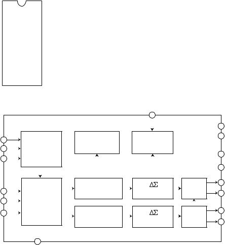
XV-N50BK,XV-N55SL
4.2 AK4381VT-X (IC402) : 2ch DAC
• Pin layout
MCLK |
1 |
16 |
DZFL |
BICK |
2 |
15 |
DZFR |
SDTI |
3 |
14 |
VDD |
LRCK |
4 |
13 |
VSS |
PDN |
5 |
12 |
AOUTL+ |
CSN |
6 |
11 |
AOUTL- |
CCLK |
7 |
10 |
AOUTR+ |
CDTI |
8 |
9 |
AOUTR- |
• |
Block diagram |
|
|
|
|
|
|
|
|
|
|
|
|
|
|
|
||
|
|
|
|
|
|
|
|
|
|
|
|
|
|
MCLK |
|
|
|
|
|
|
|
|
|
|
|
|
|
|
|
|
|
|
|
|
|
||
|
|
|
|
|
|
|
|
|
|
|
|
|
|
|
|
|
||
|
|
CSN |
|
|
|
uP |
De-emphasis |
Clock |
|
|
|
|||||||
|
|
|
|
|
Control |
Divider |
|
|
|
|||||||||
|
|
CCLK |
|
|
|
|
|
|
|
|||||||||
|
|
|
|
Interface |
|
|
|
|||||||||||
|
|
CDTI |
|
|
|
|
|
|
|
|
|
|
|
|||||
|
|
|
|
|
|
|
|
|
|
|
|
|
|
|
|
|
|
|
|
|
|
|
|
|
|
|
|
|
|
|
|
|
|
|
|
|
|
|
|
LRCK |
|
|
|
|
|
|
|
8X |
Modulator |
|
SCF |
|||||
|
|
|
|
|
|
|
|
|
|
|||||||||
|
|
|
|
|
Audio |
|
|
|||||||||||
|
|
|
|
|
|
Interpolator |
|
|
|
|||||||||
|
|
|
|
|
||||||||||||||
|
|
BICK |
|
|
|
|
Data |
|
|
|
|
|
|
|
|
|
||
|
|
|
|
|
|
|
|
|
|
|
|
|
|
|
||||
|
|
SDTI |
|
|
Interface |
|
8X |
|
|
Modulator |
|
SCF |
||||||
|
|
|
|
|
||||||||||||||
|
|
|
|
|
|
|
|
|
|
Interpolator |
|
|||||||
|
|
|
|
|
|
|
|
|
|
|
|
|
||||||
|
|
|
|
|
|
PDN |
|
|
|
|
|
|
|
|
|
|||
• |
Pin functions |
|
|
|
|
|
|
|
|
|
|
|
|
|
|
|
||
|
|
|
|
|
|
|
|
|
|
|
|
|
|
|
|
|
|
|
|
Pin No. |
Symbol |
|
I/O |
|
|
|
|
|
Description |
|
|
|
|
|
|||
|
|
|
|
|
|
|
|
|
|
|
|
|
|
|
|
|
|
|
|
1 |
MCLK |
|
I |
|
Master clock input terminal |
|
|
|
|
|
|||||||
|
|
|
|
|
|
|
|
|
|
|
|
|
|
|
|
|
|
|
|
2 |
BICK |
|
I |
|
Audio serial data clock terminal |
|
|
|
|
|
|||||||
|
|
|
|
|
|
|
|
|
|
|
|
|
|
|
|
|
|
|
|
3 |
SDTI |
|
I |
|
Audio serial data input terminal |
|
|
|
|
|
|||||||
|
|
|
|
|
|
|
|
|
|
|
|
|
|
|
|
|
|
|
|
4 |
LRCK |
|
I |
|
L/R Clock terminal |
|
|
|
|
|
|||||||
|
|
|
|
|
|
|
|
|
|
|
|
|
|
|
|
|
|
|
|
5 |
PDN |
|
I |
|
Power down mode terminal |
|
|
|
|
|
|||||||
|
|
|
|
|
|
|
|
|
|
|
|
|
|
|
|
|
|
|
|
6 |
CSN |
|
I |
|
Chip select |
|
|
|
|
|
|
|
|
|
|||
|
|
|
|
|
|
|
|
|
|
|
|
|
|
|
|
|
|
|
|
7 |
CCLK |
|
I |
|
Control data input terminal |
|
|
|
|
|
|||||||
|
|
|
|
|
|
|
|
|
|
|
|
|
|
|
|
|
|
|
|
8 |
CDTI |
|
I |
|
Control data input terminal |
|
|
|
|
|
|||||||
|
|
|
|
|
|
|
|
|
|
|
|
|
|
|
|
|
||
|
9 |
AOUTR- |
|
O |
Rch negative analog output terminal |
|
|
|
|
|
||||||||
|
|
|
|
|
|
|
|
|
|
|
|
|
|
|
|
|
|
|
|
10 |
AOUTR+ |
|
O |
|
Rch positive analog output terminal |
|
|
|
|
|
|||||||
|
|
|
|
|
|
|
|
|
|
|
|
|
|
|
|
|
|
|
|
11 |
AOUTL- |
|
O |
|
Lch negative analog output terminal |
|
|
|
|
|
|||||||
|
|
|
|
|
|
|
|
|
|
|
|
|
|
|
|
|
|
|
|
12 |
AOUTL+ |
|
O |
|
Lch positive analog output terminal |
|
|
|
|
|
|||||||
|
|
|
|
|
|
|
|
|
|
|
|
|
|
|
|
|
|
|
|
13 |
VSS |
- |
|
Connect to ground |
|
|
|
|
|
||||||||
|
|
|
|
|
|
|
|
|
|
|
|
|
|
|
|
|
|
|
|
14 |
VDD |
- |
|
Power supply terminal |
|
|
|
|
|
||||||||
|
|
|
|
|
|
|
|
|
|
|
|
|
|
|
|
|
|
|
|
15 |
DZFR |
|
O |
|
Rch data zero input detection terminal |
|
|
|
|
|
|||||||
|
|
|
|
|
|
|
|
|
|
|
|
|
|
|
|
|
|
|
|
16 |
DZFL |
|
O |
|
Lch data zero input detection terminal |
|
|
|
|
|
|||||||
|
|
|
|
|
|
|
|
|
|
|
|
|
|
|
|
|
|
|
VDD
VSS
DZFL
DZFR
AOUTL+ AOUTL-
AOUTR+ AOUTR-
1-26 (No.A0041)

XV-N50BK,XV-N55SL
4.3 AN8708FHK(IC101):Frontend processor
• Pin layout
|
|
48 |
|
37 |
|
|
|
1 |
|
|
36 |
|
|
12 |
|
|
25 |
|
|
13 |
|
24 |
|
• Pin function |
|
|
|
|
|
|
|
|
|
|
|
Pin No. |
|
Symbol |
|
I/O |
Description |
1 |
|
GND1 |
|
- |
Connect to ground |
2 |
|
LPC1 |
|
I |
Laser input terminal (DVD) |
3 |
|
LPC01 |
|
O |
Laser drive output terminal (DVD) |
4 |
|
LPC2 |
|
I |
Laser input terminal (CD) |
5 |
|
LPC02 |
|
O |
Laser drive output terminal (CD) |
6 |
|
FBAL |
|
I |
Focus balance control terminal |
7 |
|
TBAL |
|
I |
Tracking balance control terminal |
8 |
|
POFLT |
|
O |
Track detection filter terminal |
9 |
|
SEN |
|
I |
SEN (Serial data input terminal) |
10 |
|
SCK |
|
I |
SCK (Serial data input terminal) |
11 |
|
STDI |
|
I/O |
STDI (Serial data input/output terminal) |
12 |
|
VRE18 |
|
- |
RF Standard voltage filter |
13 |
|
TE |
|
O |
Tracking error signal output terminal |
14 |
|
VSS |
|
- |
Connect to ground |
15 |
|
OFTR |
|
O |
OFTR output |
16 |
|
BDO |
|
O |
BDO output |
17 |
|
VDD |
|
- |
Power supply terminal 3 (3.3V) |
18 |
|
RSCL |
|
- |
Source terminal of standard current |
19 |
|
GND2 |
|
- |
Connect to ground |
20 |
|
FE |
|
O |
Focus error signal output terminal |
21 |
|
FS |
|
O |
Focus addition signal output terminal |
22 |
|
VHALF |
|
O |
VHALF Voltage output terminal |
23 |
|
MIRSL |
|
O |
MIRROR Slow envelope detection terminal |
24 |
|
BDOSL |
|
O |
BDO Slow envelope detection terminal |
25 |
|
VCC2 |
|
- |
Power supply terminal 2 (3.3V) |
26 |
|
FLTOP |
|
O |
Filter amplifier positive output terminal |
27 |
|
FLTON |
|
O |
Filter amplifier negative output terminal |
28 |
|
SAG |
|
O |
SAG Cancel detention terminal |
29 |
|
DCAGC |
|
O |
FLT-DC Cut filter terminal |
30 |
|
AGCG |
|
O |
AGC Amp.gain control terminal |
31 |
|
TESTSG |
|
I |
TEST signal input terminal |
32 |
|
RFINP |
|
I |
RF signal positive input terminal |
33 |
|
RFINN |
|
I |
RF signal negative input terminal |
34 |
|
DCRF |
|
O |
Filter terminal for RF all addition AMP.DC cut |
35 |
|
PEAK |
|
O |
Peak envelope detection filter terminal |
36 |
|
RFENV |
|
O |
RF Envelope output terminal |
37 |
|
VCC1 |
|
- |
Power supply terminal 2 (5V) |
38,39 |
|
VIN5,6 |
|
I |
Internal four division (CD) RF input terminal 1,2 |
40,41 |
|
VIN7,8 |
|
I |
External two division (DVD) RF input terminal 1,2 |
42 |
|
VREF |
|
- |
VREF Voltage output terminal |
43~46 |
|
VIN1~4 |
|
I |
Internal four division (DVD) RF input terminal 1~4 |
47,48 |
|
VIN9,10 |
|
I |
Three beam sub (CD) input terminal 1,2 |
(No.A0041)1-27
 Loading...