

Page 1
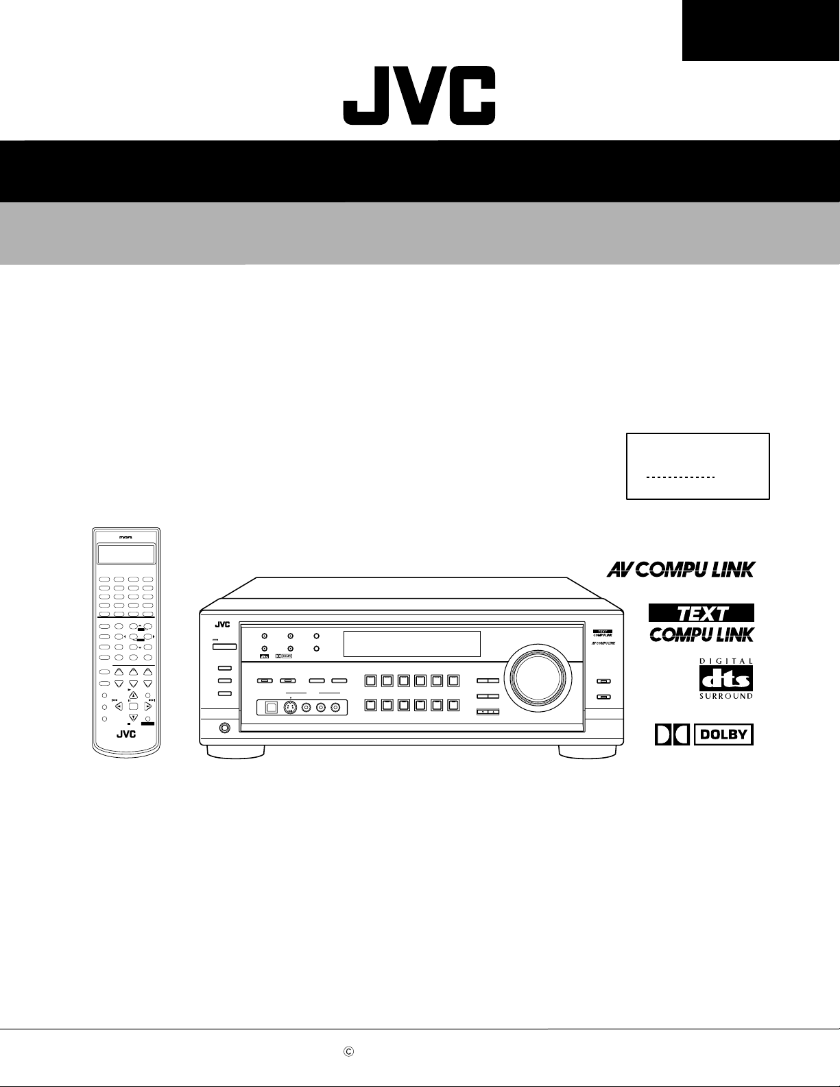
SERVICE MANUAL
AUDIO/VIDEO CONTROL RECEIVER
RX-8010VBK
RX-8010VBK
CATV/DBS VCR 1 TV AUDIO
POWER POWER
POWER
POWER
DVD MUILTIDVD
CD
FM/AM
CDR
TV/DBS VIDEO PHONO
TAPE/MD
VCR 1 VCR 2
SURROUND
LINE DIF.ECT BOOST EFFECT
MIDNIGHT
MODE
SOUND
MUTING
CATV/DBS
CONTROL
TV/VIDEO
MENU
TEXT
DISPLAY
REC
PAUSE
ANALOG/DIGITAL
DSP
MODE INPUTON/OFF
231
TEST CTR TONE
564
SUBWFR
L/R BAL∗CENTER
∗
∗
7/P
89
REAR L ∗REAR R
DIGITAL EQ
∗
∗
0 +1010
RETURN FM MODE 1 00
BAL L
∗
+−+−+
CH/
LEVELTV VOL
∗
BAL R
∗
PLAY
/REW
PAUSE
SET
DOWN – TUNING – UP
STOP
RM-SRX8010J
A/V CONTROL RECEIVER
MENU
ENTER
USB
SLEEP
ROOMBASS
SIZE
LIVENESS
VOLUME
EXIT
FF/
CONTROL
Contents
Area Suffix
J U.S.A.
RX-8010V
FM/AM TUNING FM/AM PRESET FM MODE
STANDBY
POWER
DIGITAL
+
−
SPEAKERS ON/OFF
SUBWOOFER OUT ON/OFF
PHONES
SURROUND
1
SURROUND ON/OFF
2
USB AUDIO
DIGITAL
S-VIDEO VIDEO
MEMORY
INPUT
ANALOG/DIGITAL
INPUT ATT
VIDEO
MIDNIGHT MODEDSP MODE
L—AUDIO—R
AUDIO/VIDEO CONTROL RECEIVER
SOUCE NAME
TV SOUND/DBSVIDEOVCR 2VCR 1DVDDVD MULTI
SOUCE NAME
FM / AMUSB AUDIOTAPE / MDCDRCDPHONO
DIGITAL
EQ
EFFECT SETTING
CONTROL
DOWN UP
MASTER VOLUME
LEVEL
ADJUST
LINE DIRECT
BASS BOOST
DIGITAL
Safety precautions --------------------------------------------------------1-2
Importance administering point on the safety --------------------- 1-3
Disassembly method -----------------------------------------------------1-4
Adjustment method -------------------------------------------------------1-10
Self-diagnose function ----------------------------------------------------1-11
Description of major ICs -------------------------------------------------1-13
COPYRIGHT 2001 VICTOR COMPANY OF JAPAN, LTD.
No.20921
Mar. 2001
Page 2
RX-8010VBK
1. This design of this product contains special hardware and man y circuits and components specially
for safety purposes. For continued protection, no changes should be made to the original design
unless authorized in writing by the manufacturer. Replacement parts must be identical to those
used in the original circuits. Services should be performed by qualified personnel only.
2. Alter ations of the design or circuitry of the product should not be made. Any design alterations of
the product should not be made. Any design alterations or additions will void the manufacturer`s
warranty and will further relieve the manufacture of responsibility for personal injury or property
damage resulting therefrom.
3. Many electrical and mechanical parts in the products have special safety-related characteristics.
These characteristics are often not evident from visual inspection nor can the protection afforded
by them necessarily be obtained by using replacement components rated for higher voltage,
wattage, etc. Replacement parts which have these special safety characteristics are identified in
the Parts List of Service Manual. Electrical components having such features are identified by
shading on the schematics and by ( ) on the Parts List in the Service Manual. The use of a
substitute replacement which does not have the same safety characteristics as the recommended
replacement parts shown in the Parts List of Service Manual may create shock, fire, or other
hazards.
4. The leads in the products are routed and dressed with ties, clamps, tubings, barriers and the
like to be separated from live parts, high temperature parts, moving parts and/or sharp edges
for the prevention of electric shock and fire hazard. When service is required, the original lead
routing and dress should be observed, and it should be confirmed that they have been returned
to normal, after re-assembling.
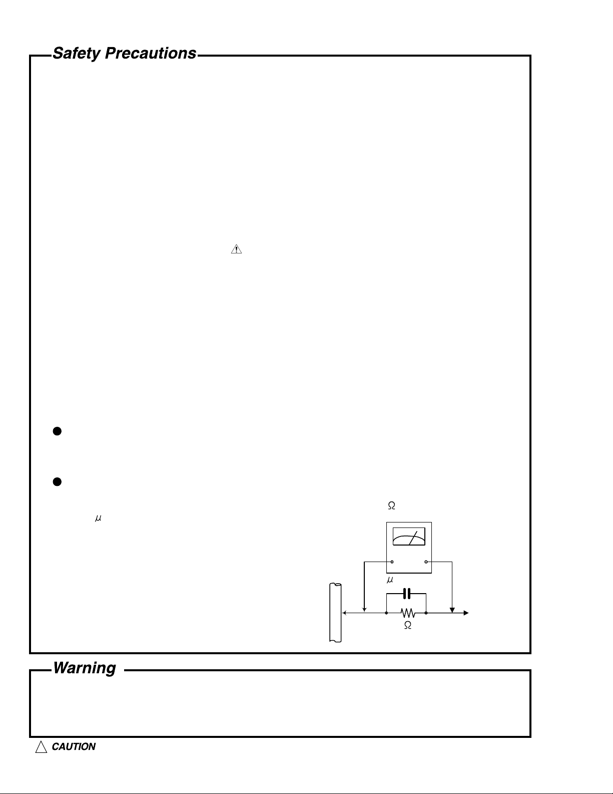
5. Leakage currnet check (Electrical shock hazard testing)
After re-assembling the product, always perform an isolation check on the exposed metal parts
of the product (antenna terminals, knobs, metal cabinet, screw heads, headphone jack, control
shafts, etc.) to be sure the product is safe to operate without danger of electrical shock.
Do not use a line isolation transformer during this check.
Plug the AC line cord directly into the AC outlet. Using a "Leakage Current Tester", measure
the leakage current from each exposed metal parts of the cabinet , particularly any exposed
metal part having a return path to the chassis, to a known good earth ground. Any leakage
current must not exceed 0.5mA AC (r.m.s.)
Alternate check method
Plug the AC line cord directly into the AC outlet. Use an AC voltmeter having, 1,000 ohms
per volt or more sensitivity in the following manner. Connect a 1,500 10W resistor paralleled by
a 0.15 F AC-type capacitor between an exposed
metal part and a known good earth ground.
Measure the AC voltage across the resistor with the
AC voltmeter.
AC VOLTMETER
(Having 1000
ohms/volts,
or more sensitivity)
Move the resistor connection to eachexposed metal
part, particularly any exposed metal part having a
return path to the chassis, and meausre the AC
voltage across the resistor. Now, reverse the plug in
the AC outlet and repeat each measurement. voltage
measured Any must not exceed 0.75 V AC (r.m.s.).
0.15 F AC TYPE
1500 10W
Place this
probe on
each exposed
metal part.
This corresponds to 0.5 mA AC (r.m.s.).
Good earth ground
1. This equipment has been designed and manufactured to meet international safety standards.
2. It is the legal responsibility of the repairer to ensure that these safety standards are maintained.
3. Repairs must be made in accordance with the relevant safety standards.
4. It is essential that safety critical components are replaced by approved parts.
5. If mains voltage selector is provided, check setting for local voltage.
!
Burrs formed during molding may be left over on some parts of the chassis. Therefore,
pay attention to such burrs in the case of preforming repair of this system.
1-2
Page 3
Importance administering point on the safety
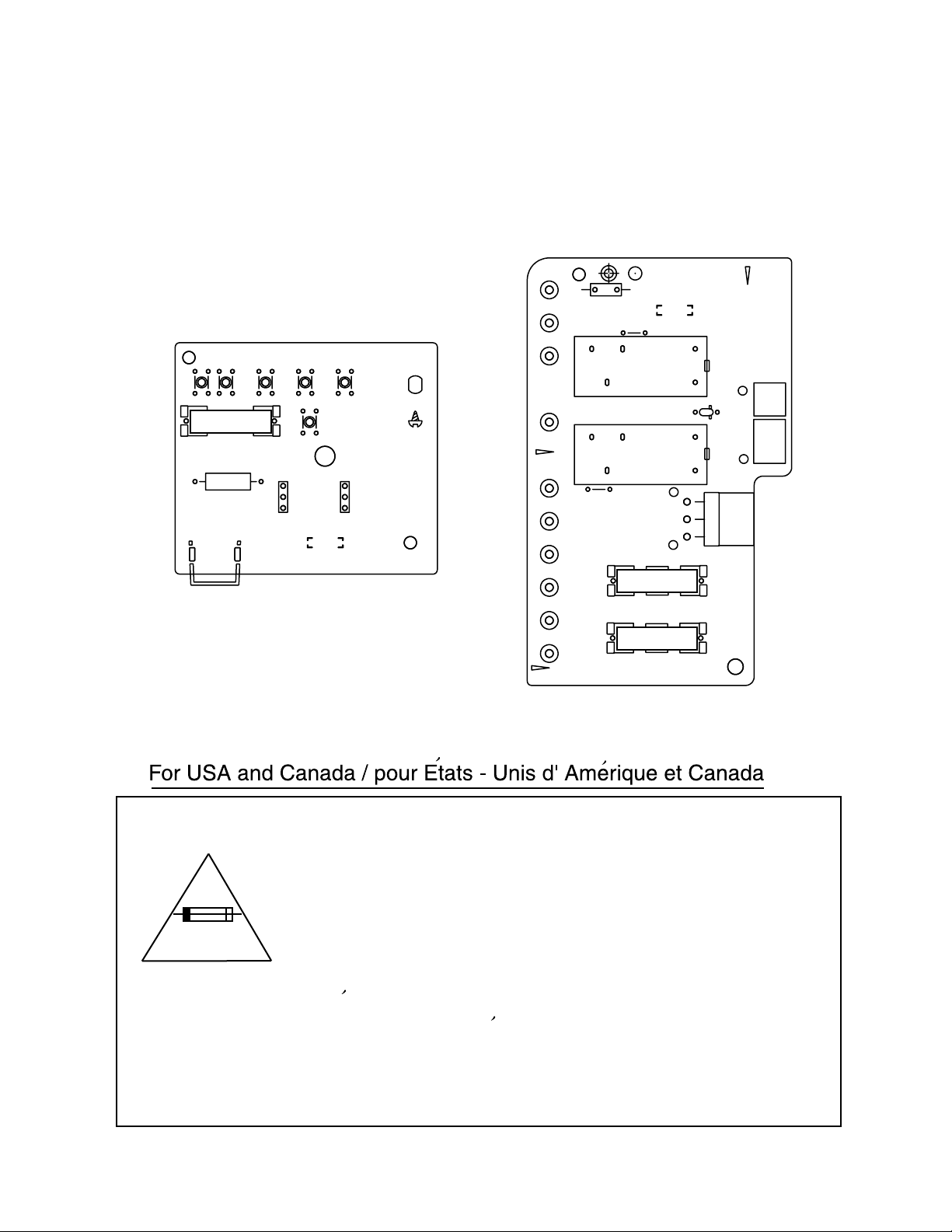
131
PW17
PW20
B3141
B3143
B3142
FC1
6.3A-125V
R61
132
PW19
PW26
PW18
B3148
B3151
B3150
B3152
PW30
TA1
B3147
B3145
B3146
B3144
FC2
B3149
TA2
R1
113
112
111
123
B3191
B3192
LVA10222-A6
RY63
RY62
RX-8010VBK
CN55
D67
CN56
CN811
EP1
122
LVA10222-A3
FC62
FC64
2A-125V
2A-125V
FC61
FC63
121
134
133
Caution: For continued protection against risk of
fire, replace only with same type 6.3A/125V for
F201, 2A/125V for F202 and F203. This symbol
specifies type of fast operating fuse.
Precaution: Pour eviter risques de feux, remplacez
le fusible de surete de F201 comme le meme type
que 6.3A/125V, et 2A/125V pour F202 et F203.
Ce sont des fusibles suretes qui functionnes rapide.
^
1-3
Page 4
RX-8010VBK
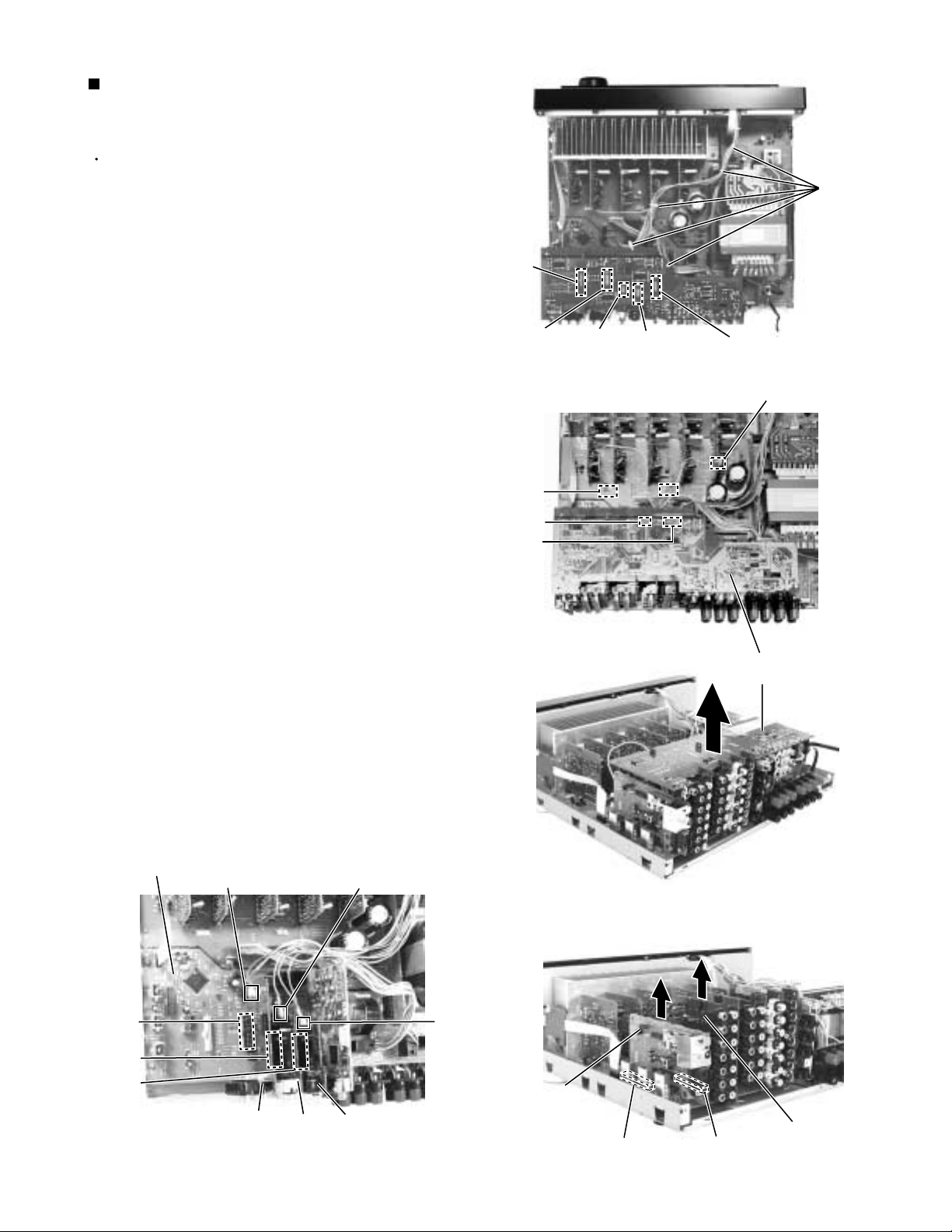
Disassembly method
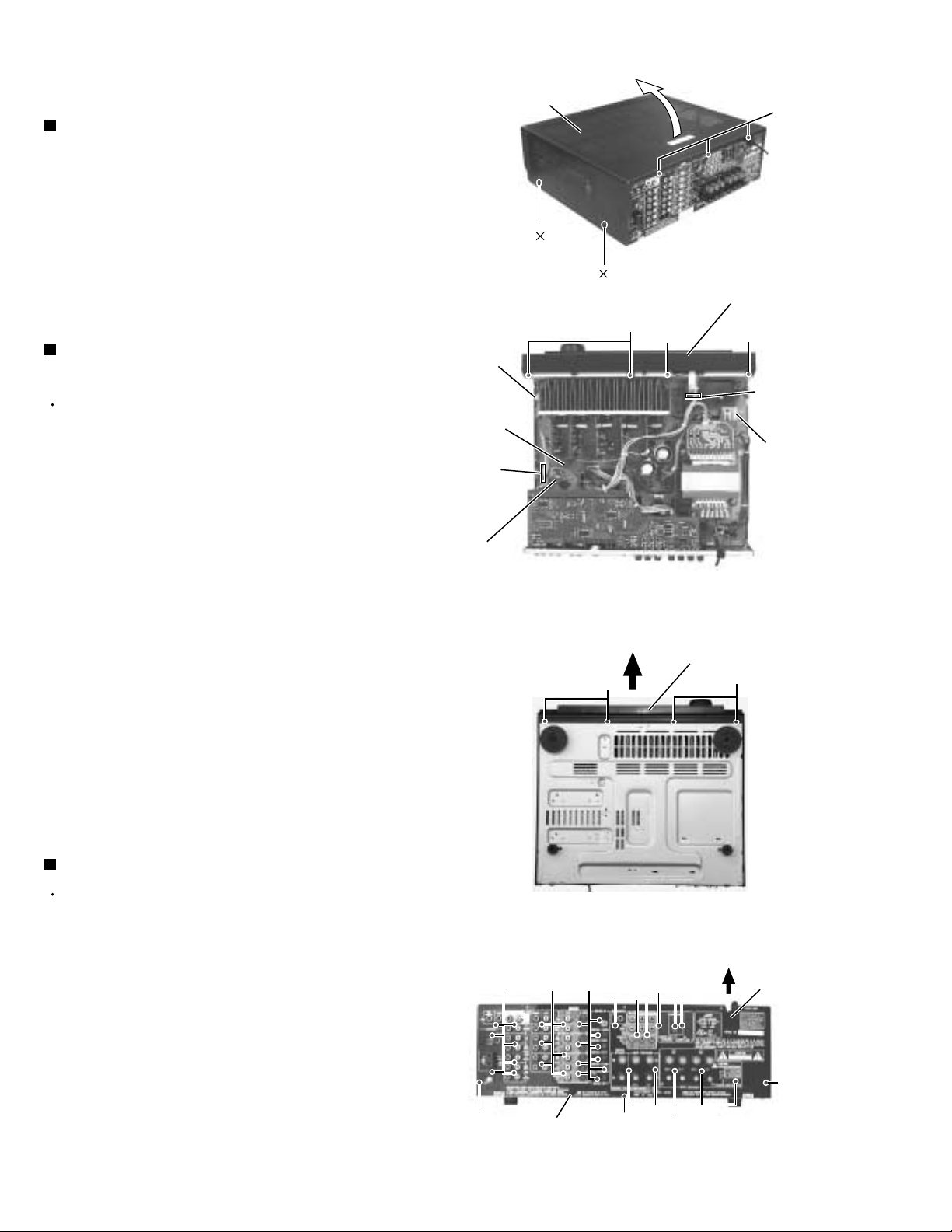
Removing the top cover (See Fig.1)
1.
Remove the four screws A attaching the top cover
on both sides of the body.
2.
Remove the three screws B on the back of the body.
3.
Remove the top cover from behind in the direction of
the arrow while pulling both sides outward.
Removing the front panel assembly
(See Fig.2 to 3)
Prior to performing the following procedure, remove
the top cover.
1.
Disconnect the card wire from connector CN400 on
the audio board and CN402 on the power supply
board in the front panel assembly.
2.
Cut off the tie band fixing the harness.
3.
Remove the three screws C attaching the front
panel assembly and the screw a fixing a ground.
Top cover
Tie band
Main
board
CN400
Audio board
A
B
2
A
2
C
Fig.2
Fig.1
Front panel assembly
a
C
CN402
Power
supply
board
4.
Remove the four screws D attaching the front panel
assembly on the bottom of the body. Detach the front
panel assembly toward the front.
Removing the rear panel (See Fig.4)
Prior to performing the following procedure, remove
the top cover.
1.
Remove the power cord stopper from the rear panel
by moving it in the direction of the arrow.
2.
Remove the thirty four screws E attaching the each
boards to the rear panel on the back of the body.
3.
Remove the three screws F attaching the rear panel
on the back of the body.
E
Front panel assembly
D
Fig.3
D
EEE
Cord stopper
F
1-4
F
Rear panel
F
Fig.4
E
Page 5
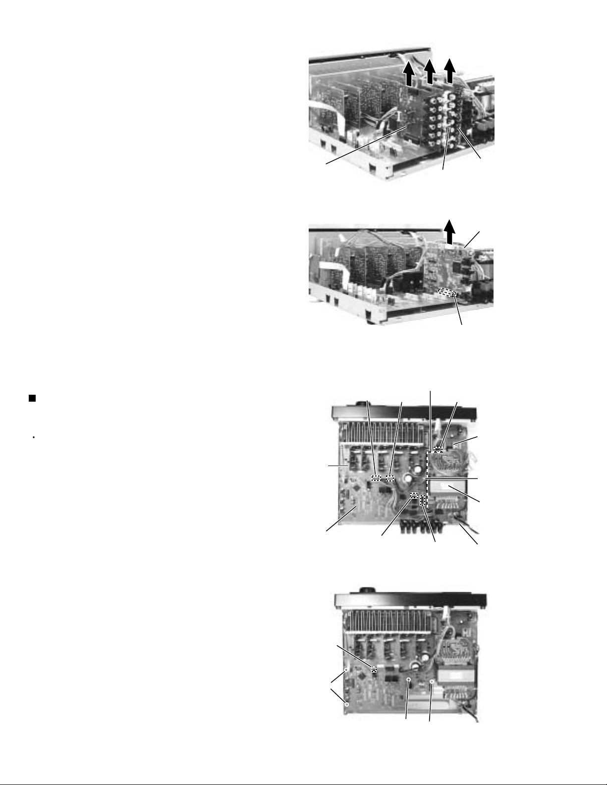
Removing each board connected to the
rear side of the audio board
(See Fig.5 to 11)
Prior to performing the following procedure, remove
the top cover and the rear panel.
1.
Cut off the tie band fixing the harness.
2.
Disconnect the connect CN501, CN243, CN205,
CN381, CN361 on the DVD board.
3.
Disconnect the harness from connector CN721,
CN722 and CN723.
4.
Disconnect the tuner board and audio board from
connector CN101 and CN301 on the audio board.
5.
Pull out the video audio board, video board, S-video
board.
6.
Disconnect the DSP board from connector CN601 on
the audio board.
CN361
CN381
CN723
CN731
CN732
CN205
CN243
Fig.5
CN721
RX-8010VBK
Tie band
CN501
CN722
CN303
CN201
CN241
Audio
board
CN416
Video audio
board
Video
board
CN206
S Video
board
CN244
Tuner
board
CN101
Fig.6
Fig.7
CN301
DVD board
Audio input
board
Fig.9
Fig.8
1-5
Page 6
RX-8010VBK
Removing the audio board
(See Fig.12 to 13)
Prior to performing the following procedure, remove
the top cover and the rear panel.
1.
Disconnect the harness from connector CN813 and
CN814 on the main board.
Video audio
board
Main
board
CN814
Fig.10
Fig.11
CN813
Video
board
CN601
Relay board
CN71
S Video
board
DSP board
power
supply
board
Tie band
2.
Disconnect the card wire from connector CN931 and
CN932 on the audio board.
3.
Cut off the tie band fixing the harness.
4.
Disconnect the relay board from the audio board and
the power supply board. (CN71,CN81)
5.
Disconnect the card wire from connector CN831 on
the main board.
6.
Remove the three screws G attaching the audio
board assembly.
7.
Remove the screw H attaching the audio board
assembly.
1-6
Audio board
CN831
G
CN931/ 932
Fig.12
Fig.13
G
CN81
H
Power
transformer
Power / Fuse
board
Page 7
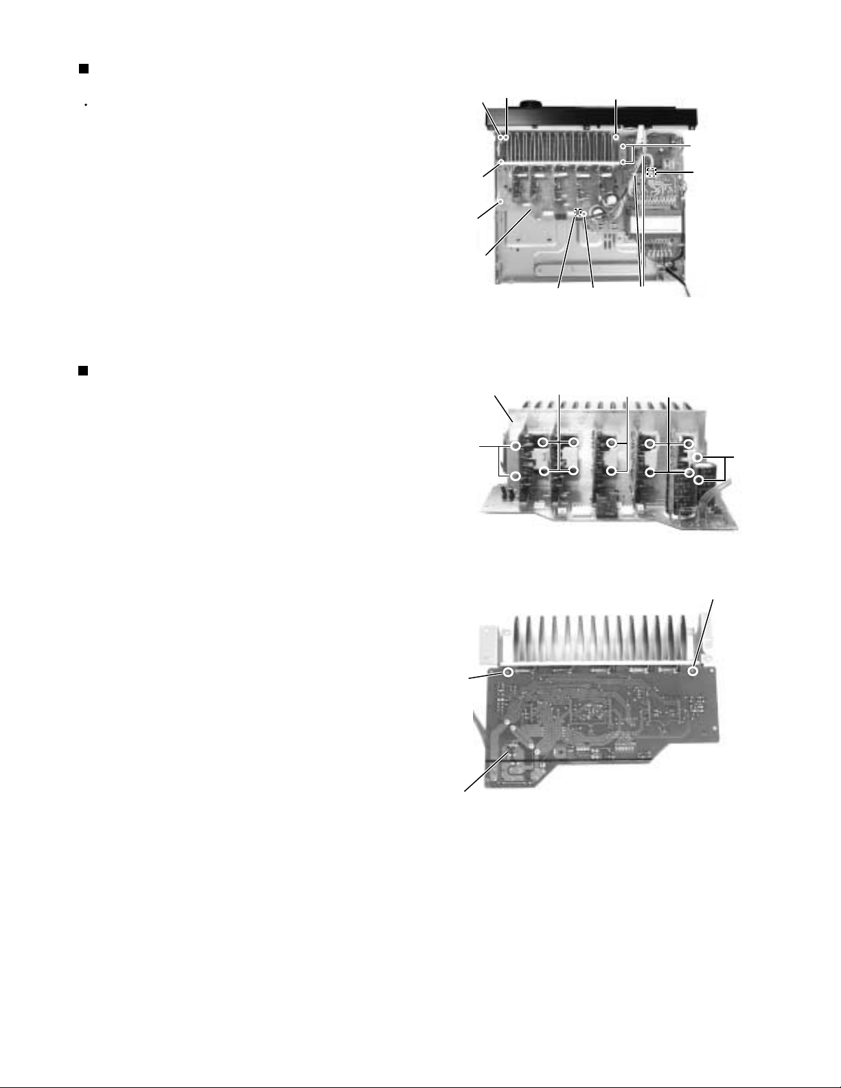
Removing the main board (See Fig.14)
Prior to performing the following procedure, remove
the top cover, the rear panel and audio board.
RX-8010VBK
I
J
I
1.
Cut off the tie band fixing the harness.
2.
Disconnect the harness from connector CN811 on
the power supply board respectively.
3.
Disconnect the harness from connector CN881 on
the main board.
4.
Remove the four screws I and the two screws J
attaching the main board.
Removing the Heat sink
(See Fig.15 to 16)
1.
Remove the ten screws K and four screws L
attaching the heat sink.
2.
Remove the two screws L' attaching the heat sink
from the rear side of main board.
J
I
Main
board
Heat sink
L
CN881
K
I
Fig.14
Tie band
K
J
CN811
K
L
L'
Main board
rear side
Fig.15
L'
Fig.16
1-7
Page 8
RX-8010VBK
Removing the power transformer
(See Fig.17)
Prior to performing the following procedures, remove
the top cover.
1.
Unsolder the two harnesses connected to the power
transformer.
2.
Disconnect the harness from connector CN55 and
CN56 on the power transformer board.
3.
Remove the four screws M attaching the power
transformer.
Power
transformer
board
CN55 / 56
Power
supply
board
M
Power
transformer
Removing the power / fuse board
(See Fig.17)
Prior to performing the following procedure, remove
the top cover and the rear panel.
1.
Remove the screw N attaching the power / fuse
board.
2.
Unsolder the power cord and other harnesses
connected to the power / fuse board.
Removing the power supply board
(See Fig.18 to 19)
Prior to performing the following procedure, remove
the top cover and the front panel.
1.
Remove the screws b fixing a bonding ground.
2.
Remove the one nut attaching the headphone jack of
the power supply board on the front side of the body.
3.
Disconnect the card wire from connector CN402 on
the power supply board.
4.
Remove the three screws O attaching the power
supply board and pull out the power supply board
from the front bracket backward.
Power
supply
board
Solder
O
Power cord
Fig.17
Fig.18
Power supply
board
M
N
Solder
Power / fuse board
b
Headphone jack
Nut
Headphone jack
5.
Unsolder the three harnesses connected to the
power supply board.
1-8
CN402
Hook
Fig.19
O
Tie band
O
Tie band
Solder
Page 9
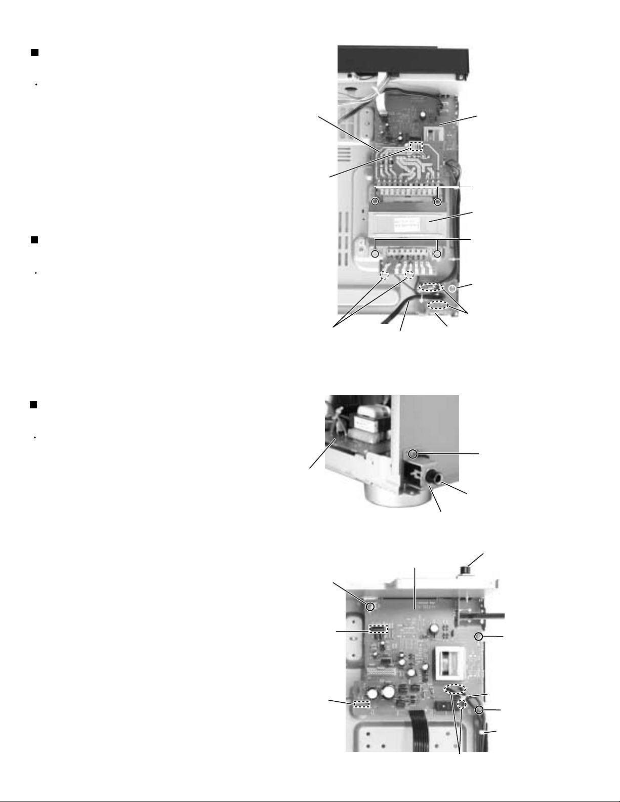
Removing the system control board /
power switch board (See Fig.20 to 22)
Prior to performing the following procedure, remove
the top cover and the front panel assembly.
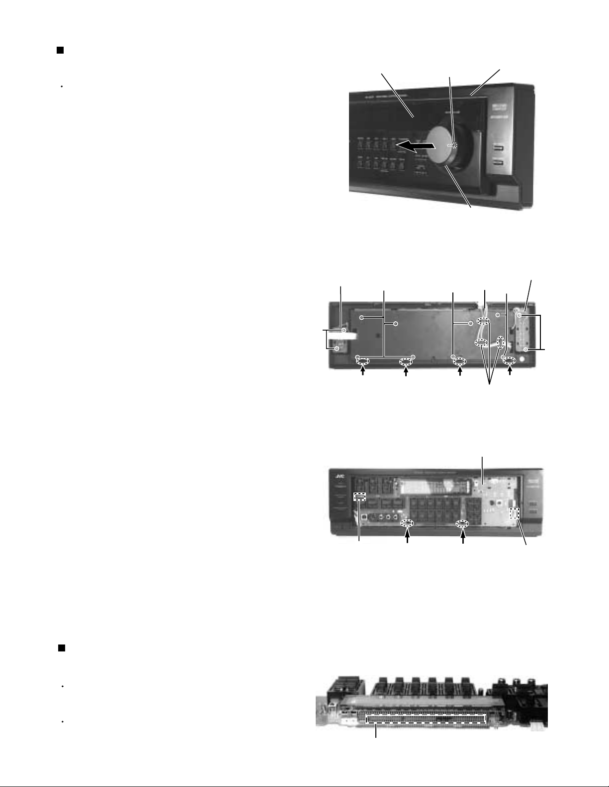
1.
Pull out the volume knob on the front side of the front
panel and remove the nut attaching the system
control board.
2.
Remove the two screws P attaching the power
switch board.
3.
Remove the two screws Q attaching the switch
board.
4.
Remove the cords from the three hooks a.
5.
Remove the eight screws R attaching the system
control board on the back of the front panel.
6.
On the back of the front panel, release the four joints
by pushing the joint tabs inward.
Remove the operation switch panel toward the front.
Operation switch panel
Switch
board
Q
R
Fig.20
Front panel assembly
Nut
Volume knob
Cords
R
RX-8010VBK
Power switch
board
R
7.
Disconnect the harness from connector CN420 and
CN422 on the system control board.
8.
Release the two hooks b attaching the system
control board.
Joint
CN420
Joint
Hook b
Joint
Hook a
Fig.21
System control board
Hook b
Fig.22
P
Joint
CN422
Matters that require attention during
replacement of IC400
In case where there is a resistance array:
Both onetime IC and mask IC can be used
In case where there is no resistance array:
Only mask IC can be used
Resistance array
1-9
Page 10

RX-8010VBK
Adjustment method
Tuner section
1.Tuner range
FM 87.5MHz~108.0MHz
AM(MW) 530kHz~1710kHz
Power amplifier section
Adjustment of idling current
Measurement location B2204-B2205(Lch) , B2213-2214(Rch)
Adjustment part VR787(Lch) , VR788(Rch)
Attention
This adjustment does not obtain a correct adjustment value immediately after the amplifier is
used (state that an internal temperature has risen).
Please adjust immediately after using the amplifier after turning off the power supply of the
amplifier and falling an internal temperature.
<Adjustment method>
1.Set the volume control to minimum during this adjustment.(No signal & No load)
2.Set the surround mode OFF.
2.Turn VR787 and VR788 fully counterclockwise to warm up before adjustment.
If the heat sink is already warm from previous use the correct adjustment can not be made.
3.For L-ch,connect a DC voltmeter between B2204 and B2205 (Lch)
And,connect it between B2213 and B2214(Rch).
4.30 minutes later after power on, adjust VR787 for L-ch, or VR788 for R-ch so that the DC voltmeter
value has 1mV~10mV.
* It is not abnormal though the idling current might not become 0mA even if it is finished to turn variable
resistance (VR787,VR788) in the direction of counterclockwise.
Heat sink
B2213, B2214
VR788 (Rch)
VR787 (Lch)
B2204, B2205
1-10
Page 11

RX-8010VBK
Self-diagnose function
1. Detection of abnormal power supply and voltage
When the power is turned ON, if an abnormality is detected during the signal input at the A/D port (IC901,
pin 2-5, 7) for one second continuously, the status will become STANDBY mode immediately.
When the power is turned ON again, detection of abnormal power supply and voltage will not be carried out
during the first 4 seconds.
Given below is a list of threshold values at the detection of abnormalities.
Pin 2
Micro-computer+5V
Pin 3
Digital+5V
Pin 4
Analog+5V
Pin 5
+12V
Pin 7
Tuner+9V
At abnormal state
(Low voltage)
Analog value
0 - 2.2V
Analog value
0 - 2.2V
Analog value
0 - 2.2V
Analog value
0 - 2.2V
Analog value
0 - 2.2V
At abnormal state
Analog value
2.2 - 2.8V
Analog value
2.2 - 2.8V
Analog value
2.2 - 2.8V
Analog value
2.2 - 2.8V
Analog value
2.2 - 2.8V
At abnormal state
(High voltage)
Analog value
2.8 - 5.0V
Analog value
2.8 - 5.0V
Analog value
2.8 - 5.0V
Analog value
2.8 - 5.0V
Analog value
2.8 - 5.0V
2. Initial setting on ship
To gain the initial setting on ship, put the power plug in the socket while pressing DOWN key and UP key
together simultaneously, then turn the power ON.
3. Test mode
To enter the test mode, put the power plug in the socket while pressing EFFECT key and UP key together
simultaneously, then turn the power ON.
Workings of test mode:
All FLs are turned ON for 3 seconds. (the FLs, which are divided in two groups, are turned ON alternatively)
A Faster volume UP/DOWN operation can be achieved with the remote controller.
When the power is turned OFF, the test mode will be released.
The FL display returns to normal after the three seconds. Then the STANDBY LED is turned ON (flashing
ON and OFF for each one second) to show the present status being a test mode.
1-11
Page 12

RX-8010VBK
4. Self-diagnose
To enter the self-diagnose mode, put the power plug in the socket while pressing SETTING key and UP key
together simultaneously, then turn the power ON. With the UP/DOWN key operation, DSP microcomputer,
ROM No.of system microcomputer as well as working status of DSP can be displayed for five seconds.
While the working status is being displayed, the followings items can be switched with the UP/DOWN key
operation.
VERSION of system microcomputer Local microcomputer CH0
Local microcomputer CH01 Local microcomputer CH2
Local microcomputer CH3 Local microcomputer CH4
When the power is turned OFF, the self-diagnose mode will be released.
During the self-diagnose mode, the STANDBY LED is turned ON .
(flashing ON for one second then OFF for three seconds)
FL transient display will be carried out as follows. When the transient display is not carried out,
normal display/workings are carried out.
FL Display
S 0 0 1 1
2 0 0 0 1 2 0 9 0 0
D 0 0
D 0 1
D 0 2
Upper 1 2 3 4 5 digits
Lower 1 2 3 4 5 6 7 8 9 10 digits
Information on VERSION of system microcomputer (IC901)
Example : VER1.1 2000/12/9
Display of communication information on DSP microcomputer (IC581)
Display of communication information on DIR AK4112A (IC551)
Display of communication information on DSP XCA56367 (IC501)
1-12
D 0 3
D 0 4 1 1
2 0 0 0 1 2 0 9 0 0
Display of communication information on CODEC AK4527 (IC571)
Information on VERSION of DSP microcomputer (IC581)
Example :VER1.1 2000/12/9
Page 13

Description of major ICs
AK4527 (IC571) : A/D,D/A Converter
1.Pin layout
LOOP1
LOOP0/SDA/CDTI
DIF1/SCL/CCLK
DIF0/CSN
P/S
MCLK
DZF1
AVSS
AVDD
VREFH
VCOM
RX-8010VBK
SDOS
OCKS
MIS
BCLK
LRCK
SDTI1
SDTI2
SDTI3
SDTO
DAUX
DFS
2.Block diagram
LIN+
LIN-
4443424140393837363534
1
2
3
4
5
6
7
8
9
10
11
1213141516171819202122
DEM1
DEM0
MCKO
DVDD
DVSSPDXTS
ICKS1
ADC
ICKS0
HPF
CAD1
CAD0
33
32
31
30
29
28
27
26
25
24
23
VREFL
RIN+
RINLIN+
LINROUT1
LOUT1
ROUT2
LOUT2
ROUT3
LOUT3
Audio
I/F
RIN+
RIN-
LOUT1
ROUT1
LOUT2
ROUT2
LOUT3
ROUT3
HPF
DA TT
DA TT
DA TT
DA TT
DA TT
DA TT
LRCK
BICK
MCLK
SDOUT
SDIN1
SDIN2
SDIN3
LPF
LPF
LPF
LPF
LPF
LPF
ADC
DAC
DAC
DAC
DAC
DAC
DAC
Block Diagram (DIR and AC-3) DSP are external parts)
DAUX
Format
Converter
SDOS
SDTO
SDTI1
SDTI2
SDTI3
1-13
Page 14

RX-8010VBK
3. Pin function (1/2)
No.
1
2
3
4
5
6
7
8
9
10
11
12
13
14
15
16
17
18
19
20
21
22
23
24
25
26
27
28
29
30
31
32
Pin name
SDOS
OCKS
MIS
BICK
LRCK
SDTI1
SDTI2
SDTI3
SDTO
DAUX
DFS
DEM1
DEM0
MCKO
DVDD
DVSS
PD
XTS
ICKS1
ICKS0
CAD1
CAD0
LOUT3
ROUT3
LOUT2
ROUT2
LOUT1
ROUT1
LINLIN+
RINRIN+
I/O
SDTO Source select pin
I
Function
"L" : Internal ADC output, "H" : DAUX input
ORed with serial control register if P/S="L".
MCKO Clock frequency select pin
I
"L" : MCLK, "H" : MCLK/2. ORed with serial control register if P/S= "L".
Connect to GND
I
Audio serial data clock pin
I
Input/Output channel clock pin
I/O
DAC1 Audio serial data input pin
I
DAC2 Audio serial data input pin
I
DAC3 Audio serial data input pin
I
Audio serial data output pin
O
AUX Audio serial data input pin
I
Double speed sampling mode pin
I
"L" : Normal speed, "H" : Double speed, the ADC is powered down.
ORed with serial control register if P/S="L".
De-emphasis pin
I
ORed with serial control register if P/S="L"
De-emphasis Pin
I
ORed with serial control register if P/S="L"
Master clock output pin
O
Digital power supply pin
Digital ground pin
Power-down & Reset pin
I
When "L", the AK4527 is powered-down and the control registers are reset
to default state. If the state of CAD0-1 changes, then the AK4527
must be reset by PDN.
X'tal oscillator Select/Test mode pin
I
"H" : X'tal Oscillator selected
"L" : External clock source selected
Input clock select 1 pin
I
Input clock select 0 pin
I
Chip address pin
I
Used during the serial control mode.
Chip address pin
I
Used during the serial control mode.
Lch #3 analog output pin
O
Rch #3 analog output pin
O
Lch #2 analog output pin
O
Rch #2 analog output pin
O
Lch #2 analog output pin
O
Rch #1 analog output pin
O
Lch analog negative Input Pin
I
Lch analog positive Input Pin
I
Rch analog negative Input Pin
I
Rch analog positive Input Pin
I
AK4527(1/2)
1-14
Page 15

RX-8010VBK
3.Pin function (2/2)
No.
33
34
35
36
37
38
39
Pin Name
VREFL
VCOM
VREFH
AVDD
AVSS
XTI
XTO
MCKI
40
41
P/S
DIF0
CS
42
DIF1
CCLK
43
LOOP0
CDTI
44
LOOP1
CDTO
I/O
I
O
I
-
I
O
I
I
I
I
I
I
I
I
I
O
AK4527(2/2)
Function
Negative voltage reference Input pin, AVSS
Common voltage output pin,AVDD/2
Large external capacitor around 2.2uF is used to reduce power-supply noise
Positive voltage reference input pin,AVDD
Analog power supply pin
Analog ground pin
X'tal input pin
X'tal output pin if XTS="H"
External master clock input pin if XTS="L"
Parallel/Serial select pin
"L" : Serial control mode, "H" : Parallel control mode
Audio data interface format pin in parallel mode
Chip select pin in serial mode
Audio data interface format pin in parallel mode
Control data clock pin in serial mode
Loop back mode pin in parallel mode
Enables digital loop-back from ADC to 3 DACs.
Control data input pin in serial mode
Loop back mode pin in parallel mode
Enable all 3 DAC channels to be input from SDTII.
Control data output pin in serial mode
1-15
Page 16

RX-8010VBK
BA15218F(IC303, IC304, IC372, IC385, IC386) : OP AMP.
1OUT1
2-IN1
-
8
7
V
CC
OUT2
1
3+IN1
+
-
-IN2
6
2
EE
4
+
5V
+IN2
BA7625 (IC201, IC242) : Video selector
MONITOR OUT
GND
IN5
GND
IN4
CTL E
IN3
CTL D
1
2
3
4
5
6
7
8
logic
logic
16
15
14
13
12
11
10
11
IN1
CTL A
VOUT 1
CC
V
IN2
CTL B
VOUT 2
CTL C
A B E MONITOR OUT
LL
HL
LH
H H L IN4
H H H IN5
*
*
*
IN1
IN2
IN3
C D E VOUT1
LL
HL
LH
H H L IN4
H H H IN5
*
*
*
-IN2
IN3
C D E VOUT2
LL
HL
LH
H H L IN4
H H H IN5
*
*
*
IN1
-IN3
BA7626 (IC241) : Video selector
MONITOR OUT
1-16
GND
IN5
GND
IN4
CTL E
IN3
CTL D
1
2
3
4
5
6
7
8
logic
logic
16
15
14
13
12
11
10
11
IN1
CTL A
VOUT 1
V
CC
IN2
CTL B
VOUT 2
CTL C
A B E MONITOR OUT
LL
HL
LH
H H L IN4
H H H IN5
*
*
*
IN1
IN2
IN3
C D E VOUT1
LL
HL
LH
H H L IN4
H H H IN5
*
*
*
-IN2
IN3
C D E VOUT2
LL
HL
LH
H H L IN4
H H H IN5
*
*
*
IN1
--
IN3
Page 17

BU2092(IC402):PORT EXPANDER
1.Terminal Layout
RX-8010VBK
Vss
DATA
CLOCK
LCK
Q0
Q1
Q2
Q3
Q4
1
2
3
4
5
6
7
8
9
CONTROL
CIRCUIT
12BIT SHIFT RESISTER
12BIT STRAGE RESISTER
OUTPUT BUFFER(OPEN DRAIN)
13
10
18
17
16
15
14
12
11
Vdd
OE
Q11
Q10
Q9
Q8
Q7
Q6
Q5
2.Pin Function
Pin No.
1
2
3
4
5~16
17
18
Symbol
Vss
DATA
CLOCK
LCK
Q0~Q11
OE
Vdd
I/O
I
I
I
O
I
-
Function
Connect to GND
Serial Data input
Shift Clock of Data
Latch Clock of Data
Parallel Data Output
Latch Data L H
OUTPUT ON OFF
Output Enable
Power Supply
1-17
Page 18

RX-8010VBK
MB90088 (IC203) : On screen display controller
1.Terminal Layout
YIN
VIN
CIN
AVcc
IOUT
VOC
Vcc
EXS
XS
HSYNC
VSYNC
EXHSYN
EXVSYN
Vss
2.Block Diagram
SIN
SCLK
CS
EXHSYN
EXVSYN
1
2
3
4
5
6
7
8
9
10
11
12
13
14
28
AVss
27
YOUT
26
VOUT
25
COUT
24
CS
23
SIN
22
SCLK
21
TEST
20
BOUT
19
ROUT
18
GOUT
17
VOB
16
XD
15
EXD
Serial Input
Control
H/V Separate
Each Control, Data
VIN
YIN
CIN
HSYNC
VSYNC
XS
EXS
XD
EXD
NTSC/PAL
Signal OSC
Display Memory
Control
VRAM
4FSC CLK
OSC
Dot CLK
OSC
Each Block
Each Block
Analog SW
Video Signal
OSC
Output
Control
CGROM
VOUT
YOUT
COUT
BOUT
ROUT
GOUT
IOUT
VOC
VOB
1-18
Page 19

3.Functions
pin
Symbol I/O Function
no
YIN
1
2
3
4
5
6
7
8
9
10
11
12
13
14
15
16
17
18
19
20
21
22
23
24
25
26
27
28
VIN
CIN
AVcc
IOUT
VOC
Vcc
EXS
XS
HSYNC
VSYNC
EXHSYN
EXVSYN
Vss
EXD
XD
VOB
GOUT
ROUT
BOUT
TEST
SCLK
SIN
CS
COUT
VOUT
YOUT
AVss
I
Lux signal Input terminal for Superinpause indication
I
Composite video signal input terminal for Superinpause indication
Contrast signal input terminal for Superinpause indication
I
-
Analog power supply terminal
O
Color (Lux) signal output terminal
Character output terminal
O
Power supply terminal
Clock generater outside circuit terminal for color burst
I
O
O
Horizontal signal output terminal
O
Vertical signal output terminal
EXT horizontal signal input terminal
I
EXT vertical signal input terminal
I
GND
Dot clock generater outside circuit signal terminal for indication
I
O
Character & background signal output terminal
O
Color signal (Green, Red, Blue)
O
I
Test signal input terminal
Shift clock input terminal for serial transmission
I
Serial data input terminal
I
Chip select terminal
I
Contrast signal output terminal
O
Composite video signal output terminal
O
Lux signal output terminal
O
Analog GND terminal
-
RX-8010VBK
1-19
Page 20

RX-8010VBK
MAX4018ESD (IC390) : OP AMP.
ENA
ENC
ENB
Vcc
INA+
INA-
OUTA
N.C.
1
2
3
4
5
6
7
8
16
15
14
13
12
11
10
OUTC
INCINC+
V
EE
INB+
INBOUTB
N.C.
9
NJM2285V-W(IC202) : 2-INPUT 3CHANNEL VIDEO SWITCH
IN1A GND1 IN2B V CTL2 IN2A GND3 IN3B
16 15 14 13 12 11 10 9
BIAS TYPE
L
+
CLAMP TYPE
H
L
CLAMP TYPE
H
H
1 2 3 4 5 6 7 8
IN1B CTL1 OUT1 GND2 OUT2 OUT3 CTL3 IN3A
L
1-20
Page 21

NJM4580D (IC301) : LPF, Mic and H.phone Amp.
1.Terminal layout
RX-8010VBK
2.Block diagram
+
V
INPUT
+
A OUT
A -IN
A +IN
V
1
2
A
3
-
4
(TOP VIEW)
B
8
7
6
5
+
V
B OUT
B -IN
B +IN
-
V
NJU7241F33(IC411) : VOLTAGE REGULATOR
PIN FUNCTION
1
5
2
3
4
1. GND
2. VIN
3. VOUT
4. +NC
5. STB
OUTPUT
1-21
Page 22

RX-8010VBK
PCM2702E-X (IC410) : DIGITAL / ANALOG CONVERTER
1.Pin layout
XTI
1
DD
C
V
2
DGNDC
3
DD
V
4
DGND
5
D+
6
D-
7
BUS
V
8
DGND
9
PLYBCK
10
SSPND
11
ZERO
12
TEST3
13
TEST2
14
3.Pin function
XTO
VccP
AGNDP
VccL
AGNDL
OUT
V
Vcc
COM
V
AGND
OUT
V
AGNDR
VccR
TEST0
TEST1
2. Block diagram
PLYBCK
28
27
26
25
24
L
23
22
21
20
R
19
18
17
16
15
D+
D-
VBUS
DGNDU
VDDC
DGNDC
SSPDN
USB I/F
MCLK
USB clock
generator
Crystal OSC
XTI
XTO
USB packet
data
WRCLK
FIFO
SPACT
audio
data
RDCLK
ZERO
8x
Oversampling
Digital Filter
System Clock
Audio clock
generator
DGNDP
VDDP
Multi-level
Delta-Sigma
Modulator
VccL
AGNDL
VccR
AGNDR
DAC
DAC
Power supply
VCC AGND VDD DGND
Low-pass
Filter
Low-pass
Filter
VOUTL
VCOM
VOUTR
PIN
1
2
3
4
5
6
7
8
9
10
11
12
13
14
15
16
17
18
19
20
21
22
23
24
25
26
27
28
Symbol
XTI
DD
C
V
DGNDC
DD
V
DGND
D+
D-
BUS
V
DGNDU
PLYBCK
SSPND
ZERO
TEST3
TEST2
TEST1
TEST0
VccR
AGNDR
OUT
R
V
AGND
COM
V
Vcc
OUT
L
V
AGNDL
VccL
AGNDP
VccP
XTO
I/O
IN
-
-
-
I/O
I/O
IN
-
OUT
OUT
OUT
IN
IN
IN
IN
-
-
OUT
-
-
-
OUT
-
-
-
-
OUT
Function
Crystal Oscillator Input.
Digital Power Supply for Clock Generator, +3.3V.
Digital Ground for Clock Generator.
Digital Power Supply, +3.3V.
Digital Ground.
USB Differential Input/Output Plus.
USB Differential Input/Output Minus.
USB Bus Power (This pin NEVER consumes the USB bus power).
Digital Ground for USB Transceiver.
Playback flag, active LOW. (LOW: playback, HIGH: idle).
Suspend flag, active LOW. (LOW: suspend, HIGH: operational).
Zero flag, (LOW: Normal, HIGH: ZERO).
Test pin 3. Connect to digital ground.
Test pin 2. Connect to digital ground.
Test pin 1. Connect to digital ground.
Test pin 0. Connect to digital ground.
Analog Supply for R-channel, +5V.
Analog Ground for R-channel.
Analog Output for R-channel.
Analog Ground.
Common for DAC.
Analog Supply, +5V.
Analog output for L-channel.
Analog Ground for L-channel.
Analog Supply for L-channel, +5V.
Analog Ground for PLL.
Analog Supply for PLL, +5V.
Crystal Oscillator Output.
(1)
(2)
(2)
(2)
(2)
(2)
1-22
Note:
(1) 3.3V tolerant.
(2) Schmitt trigger input with internal pull-down, 5V tolerant.
Page 23

TC9162AN (IC380) : ANALOG SWITCH
RX-8010VBK
VSS
L-S1
L-S2
L-COM1
L-S3
L-S4
L-COM2
L-S5
L-S6
L-COM3
L-S7
L-COM4
ST
GND
2
L-S1
1
2
3
4
5
6
7
8
9
10
11
12
13
14
28
27
26
25
24
23
22
21
20
19
18
17
16
15
VDD
R-S1
R-S2
R-COM1
R-S3
R-S4
R-COM2
R-S5
R-S6
R-COM3
R-S7
R-COM4
DATA
CK
VSS
GND VDD
1
14
28
27
R-S1
L-S2
L-COM1
L-S3
L-S4
L-COM2
L-S5
L-S6
L-COM3
L-S7
L-COM4
ST
3
4
5
6
7
8
9
10
11
12
13
LEVEL SHIFTER
LATCH CIRCUIT
LATCH CIRCUIT
LEVEL SHIFTER
26
25
24
23
22
21
20
19
18
17
16
R-S2
R-COM1
R-S3
R-S4
R-COM2
R-S5
R-S6
R-COM3
R-S7
R-COM4
DATA
SHIFT REGISTER
15
CK
1-23
Page 24

RX-8010VBK
TC9163AF-X (IC371) : ANALOG SWITCH
VSS
L-S1
L-S2
L-S3
L-COM1
L-S4
L-S5
L-S6
L-COM2
L-S7
L-S8
L-COM3
ST
GND
L-S1
L-S2
1
2
3
4
5
6
7
8
9
10
11
12
13
14
2
3
28
27
26
25
24
23
22
21
20
19
18
17
16
15
VDD
R-S1
R-S2
R-S3
R-COM1
R-S4
R-S5
R-S6
R-COM2
R-S7
R-S8
R-COM3
DATA
CK
VSS
GND VDD
1
14
28
27
26
R-S1
R-S2
L-S3
L-COM1
L-S4
L-S5
L-S6
L-COM2
L-S7
L-S8
L-COM3
ST
10
11
12
13
4
5
6
7
8
9
LEVEL SHIFTER
LATCH CIRCUIT
LATCH CIRCUIT
LEVEL SHIFTER
SHIFT REGISTER
25
24
23
22
21
20
19
18
17
16
15
R-S3
R-COM1
R-S4
R-S5
R-S6
R-COM2
R-S7
R-S8
R-COM3
DATA
CK
1-24
Page 25

TC9164AF-X (IC302) : ANALOG SWITCH
RX-8010VBK
VSS
L-S1
L-S2
L-S3
L-S4
L-COM1
L-S5
L-S6
L-COM2
L-S7
L-S8
L-COM3
ST
GND
L-S1
L-S2
1
2
3
4
5
6
7
8
9
10
11
12
13
14
2
3
28
27
26
25
24
23
22
21
20
19
18
17
16
15
VDD
R-S1
R-S2
R-S3
R-S4
R-COM1
R-S5
R-S6
R-COM2
R-S7
R-S8
R-COM3
DATA
CK
VSS
GND VDD
1
14
28
27
26
R-S1
R-S2
L-S3
L-S4
L-COM1
L-S5
L-S6
L-COM2
L-S7
L-S8
L-COM3
ST
4
5
6
7
8
9
10
11
12
13
LEVEL SHIFTER
LATCH CIRCUIT
SHIFT REGISTER
LATCH CIRCUIT
LEVEL SHIFTER
25
24
23
22
21
20
19
18
17
16
15
R-S3
R-S4
R-COM1
R-S5
R-S6
R-COM2
R-S7
R-S8
R-COM3
DATA
CK
1-25
Page 26

RX-8010VBK
TC9459F (IC381, IC382, IC383) : Electronic volume control
1.Terminal layout
VSS
L-OUT
NC
L-ch
L-IN
L-LD1
L-LD2
L-A-GND
NC
CS1
NC
GND
CK
2. Block diagram
VSS
1
1
2
3
4
5
6
7
8
9
10
11
12
24
23
22
21
20
19
18
17
16
15
14
13
VDD
R-OUT
NC
R-IN
R-LD1
R-LD2
R-A-GND
NC
CS2
NC
STB
DATA
R-ch
L-OUT
NC
L-1N
L-LD1
L-LD2
L-A-GND
NC
CS1
NC
GND
CK
9
10
11
12
2
3
4
5
6
7
8
50k /
915TEP
VR
L-ch 7 to 91
decoder
L-ch data
latch circuit
Shift register (24BIT)
Level shift circuit
VDD
24
R-ch 7 to 91
decoder
R-ch data
latch circuit
Same as L-ch
Circuit
23
22
21
20
19
18
17
16
15
14
13
R-OUT
NC
R-IN
R-LD1
R-LD2
R-A-GND
NC
CS2
NC
STB
DATA
3.Pin function
Pin No.
1
2
3
4
5
6
7
8
9
10
11
12
Symbol
VSS
L-OUT
NC
NC
L-LD1
L-LD2
L-A-GND
NC
CS1
NC
NC
CK
Function
Negative power supply pin
Volume output pin
No connection
No connection
Loudness tap output pin
Loudness tap output pin
Analog GND pin
No connection
Chip select input pin
No connection
No connection
Clock input pin
Pin No.
13
14
15
16
17
18
19
20
21
22
23
24
Symbol
DATA
STB
NC
CS2
NC
R-A-GND
R-LD2
R-LD1
R-IN
NC
R-OUT
VDD
Function
Data input pin
Strobe input pin
No connection
Chip select input pin
No connection
Analog GND pin
Loudness tap output pin
Loudness tap output pin
Volume input pin
No connection
Volume output pin
Positive power supply pin
1-26
Page 27

PQ3DZ53 (IC583) : Regulator IC
RX-8010VBK
DC INPUT(Vin)
1
CUSTOM IC
5
GND
TC74HC4053AF (IC388, IC389) : MULTIPLEXER
1Y
0Y
Z-COM
0Z
INH
V
GND
EE
1
2
IZ
3
4
5
6
7
8
16
15
14
13
12
11
10
9
Vcc
Y-COM
X-COM
1X
0X
A
B
C
CONTROL INPUTS
INHIBIT
L
L
L
L
L
L
L
L
H
X: Don't Care.
3
DC OUTPUT(Vo)
ON/OFF CONTROL(Vc)
2
C
B
A
L
L
K
L
L
H
L
H
K
L
H
H
H
L
K
H
L
H
H
H
K
H
H
H
X
X
X
W24L010AJ-12 (IC511) : CMOS STATIC RAM
1. Pin layout
1
A11
2
A9
3
A8
4
A13
5
WE
6
CS2
7
A15
8
VDD
9
NC
10
A16
11
A14
12
A12
13
A7
14
A6
15
A5
16
A4
NC
A16
A14
A12
I/O1
I/O2
I/O3
Vss
1
2
3
4
5
A7
6
A6
7
A5
8
A4
9
A3
10
A2
11
A1
12
A0
13
14
15
16
32-pin
TSOP
V
DD
32
A15
31
CS2
30
WE
29
A13
28
A8
27
A9
26
A11
25
OE
24
A10
23
CS1
22
I/O8
21
I/O7
20
I/O6
19
I/O5
18
I/O4
17
32
OE
31
A10
30
CS1
29
I/O8
28
I/O7
27
I/O6
26
I/O5
25
I/O4
24
Vss
23
DO3
22
DO2
21
DO1
19
A0
18
A1
17
A2
16
A3
2. Block diaglam
DD
V
Vss
A0
DECODER
A16
CS2
CS1
CONTROL
OE
WE
3. Pin function
SYMBOL
A0 - A16
I/O1 - I/O8
CS1, CS2
WE
OE
DD
V
Vss
NC
CORE
ARRAY
DATA I/O
I/O1
I/O8
DESCRIPTION
Address Input
Data Input/Output
Chip Select Inputs
Write Enable Input
Output Enable Input
Power Supply
Ground
No Connection
1-27
Page 28

RX-8010VBK
UPD784215AGC132(IC581) : UNIT CPU
1.Pin layout
75 ~ 51
76
~
50
~
100
1 ~ 25
26
2.Pin function
Pin No. Symbol I/O Function
1~8
9
10
11
12
13
14
15
16
17
18
19~22
23
24
25~32
33
34,35
36
37,38
39
40
41
42
43
44
45,46
47
48
49
50,51
52
53
54
55
56
57~63
64,65
66
67
68~70
71
72
73~75
76
77
78
79,80
81
82,83
84
85
86
87
88
89~93
94
95~100
VDD
X2
X1
VSS
XT2
XT1
RESET
AUTO
ERR
Fz96k
P03~P06
AVDD
AV REF0
P10~P17
AVSS
P130, P131
AV REF1
RX, TX
DSPCOM
DSPSTS
DSPCLK
DSPRDY
MIDIO_IN/OUT
MICK
HREQ
SS
DSP_RST
D_CS
PD/ DIR
CDTI/CDTO
CCLK
CS
PD
GND
EQ
CTR TONE
3D
VDD
ANA_TT
LEF_MIX
LEF_OUT
MIX_OUT
S_MUTE
TEST
Non connect
Power supply terminal
Connecting the crystal oscillator for system main clock
Connecting the crystal oscillator for system main clock
I
Connect to GND
Connecting the crystal oscillator for system sub clock
Connect VSS
I
System reset signal input
I
Output of DSP to general-purpose port
I
Output of DSP to general-purpose port
I
Output of DSP to general-purpose port
I
Output of DSP to general-purpose port
I
Power supply terminal
Connect to GND
Connect to GND
Connect to GND
Non connect
O
Power supply terminal
Not use
O
Non connect
O
Communication port from IC901
I
Status communication port to IC901
O
Clock input from IC901
I
Ready signal input from IC901
I
Non connect
O
Interface I/O terminal with microcomputer
I/O
Interface I/O terminal with microcomputer of clock signal
O
HREQ
I
System slave select
O
Non connect
Reset signal output of DSP
O
Non connect
Chip setselct output
O
Non connect
Reset signal output
O
Non connect
Interface I/O terminal with microcomputer
O/I
Interface I/O terminal with microcomputer of clock signal
O
CS
O
Non connect
Reset signal output
O
Connect to GND
Non connect
EQ
O
CENTER TONE
O
3D-Phonic
O
Non connect
Power supply
Non connect
Analog./T.TONE
O
Select 1
O
Select 2
O
Select 3
O
S.MUTE
O
Non connect
Test terminal
Non connect
-
1-28
Page 29

RX-8010VBK
VICTOR COMPANY OF JAPAN, LIMITED
AUDIO & COMMUNICATION BUSINESS DIVISION
PERSONAL & MOBILE NETWORK BUSINESS UNIT. 10-1,1chome,Ohwatari-machi,Maebashi-city,371-8543,Japan
(No.20921)
Printed in Japan
200103(V)
 Loading...