

Page 1
SERVICE MANUAL
CD RECEIVER
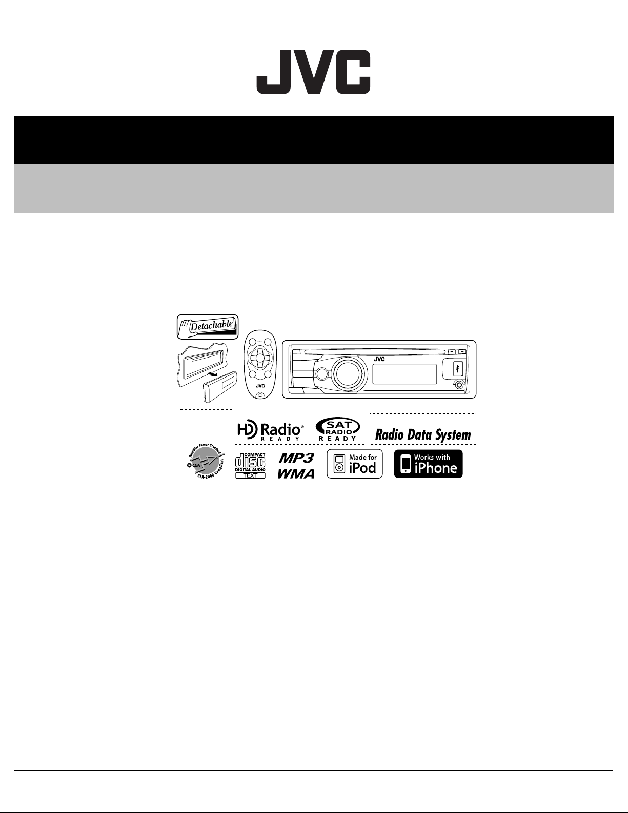
MA467<Rev.002>20106SERVICE MANUAL
KD-A615J, KD-R610J, KD-R611E, KD-R611EU,
KD-R611EY, KD-R612E, KD-R616U, KD-R616UH,
KD-R616UN, KD-R618J
KD-R618
KD-A615
KD-R610
COPYRIGHT © 2010 Victor Company of Japan, Limited
Lead free solder used in the board (material : Sn-Ag-Cu, melting point : 219 Centigrade)
Lead free solder used in the board (material : Sn-Cu, melting point : 230 Centigrade)
KD-A615 / KD-R610
only KD-R611/KD-R612
TABLE OF CONTENTS
1 PRECAUTION. . . . . . . . . . . . . . . . . . . . . . . . . . . . . . . . . . . . . . . . . . . . . . . . . . . . . . . . . . . . . . . . . . . . . . . . . 1-5
2 SPECIFIC SERVICE INSTRUCTIONS . . . . . . . . . . . . . . . . . . . . . . . . . . . . . . . . . . . . . . . . . . . . . . . . . . . . . . 1-9
3 DISASSEMBLY . . . . . . . . . . . . . . . . . . . . . . . . . . . . . . . . . . . . . . . . . . . . . . . . . . . . . . . . . . . . . . . . . . . . . . . 1-9
4 ADJUSTMENT . . . . . . . . . . . . . . . . . . . . . . . . . . . . . . . . . . . . . . . . . . . . . . . . . . . . . . . . . . . . . . . . . . . . . . . 1-18
5 TROUBLESHOOTING . . . . . . . . . . . . . . . . . . . . . . . . . . . . . . . . . . . . . . . . . . . . . . . . . . . . . . . . . . . . . . . . . 1-23
COPYRIGHT © 2010 Victor Company of Japan, Limited
No.MA467<Rev.002>
2010/6
Page 2
SPECIFICATION
KD-R618/KD-A615/KD-R610
AUDIO AMPLIFIER SECTION
Power Output 20 W RMS × 4 Channels at 4 Ω and < 1% THD+N
Signal-to-Noise Ratio 80 dBA (reference: 1 W into 4 Ω)
Load Impedance 4 Ω (4 Ω to 8 Ω allowance)
Tone Control Range Bass ±12 dB (60 Hz, 80 Hz, 100 Hz, 200 Hz) Q1.0, Q1.25, Q1.5, Q2.0
Middle ±12 dB (0.5 kHz, 1.0 kHz, 1.5 kHz, 2.5 kHz) Q0.75, Q1.0, Q1.25
Treble ±12 dB (10.0 kHz, 12.5 kHz, 15.0 kHz, 17.5 kHz) Q (Fixed)
Frequency Response 40 Hz to 20 000 Hz
Line-Out Level/Impedance KD-R618/KD-A615 5.0 V/20 kΩ load (full scale)
KD-R610 2.5 V/20 kΩ load (full scale)
Output Impedance 1 kΩ
Other Terminal AUX (auxiliary) input jack, USB input jack, Antenna input, Expansion port, Steering wheel remote input
(for KD-R618/KD-A615)
TUNER SECTION
Frequency Range FM with channel interval set to 100 kHz or 200 kHz 87.5 MHz to 108.0 MHz
with channel interval set to 50 kHz 87.5 MHz to 108.0 MHz
AM with channel interval set to 10 kHz 530 kHz to 1 710 kHz
with channel interval set to 9 kHz 531 kHz to 1 602 kHz
FM Tuner Usable Sensitivity 9.3 dBf (0.8 µV/75 Ω)
50 dB Quieting Sensitivity 16.3 dBf (1.8 µV/75 Ω)
Alternate Channel Selectivity (400 kHz) 65 dB
Frequency Response 40 Hz to 15 000 Hz
Stereo Separation 40 dB
AM Tuner Sensitivity 20 µV
Selectivity 40 dB
CD PLAYER SECTION
Type Compact disc player
Signal Detection System Non-contact optical pickup (semiconductor laser)
Number of Channels 2 channels (stereo)
Frequency Response 5 Hz to 20 000 Hz
Dynamic Range 96 dB
Signal-to-Noise Ratio 98 dB
Wow and Flutter Less than measurable limit
MP3 Decoding Format: (MPEG1/2 Audio Layer 3) Max. Bit Rate: 320 kbps
WMA (Windows Media
USB SECTION
USB Standard USB 1.1, USB 2.0
Data Transfer Rate (Full Speed) Max. 12 Mbps
Compatible Device Mass storage class
Compatible File System FAT 32/16/12
Playable Audio Format MP3/WMA
Max. Current DC 5 V 500 mA
GENERAL
Power Requirement Operating Voltage DC 14.4 V (11 V to 16 V allowance)
Grounding System Negative ground
Allowable Operating Temperature 0°C to +40°C (32°F to 104°F)
Dimensions (W × H × D):
(approx.)
Mass 1.3 kg (excluding accessories)
Designs & specifications are subject to change without notice.
® Audio) Decoding Format Max. Bit Rate: 320 kbps
Installation Size 182 mm × 52 mm × 160 mm (7-3/16" × 2-1/16" × 6-5/16")
Panel Size 188 mm × 58 mm × 6 mm (7-7/16" × 2-5/16" × 1/4")
1-2 (No.MA467<Rev.002>)
Page 3
KD-R616
AUDIO AMPLIFIER SECTION
Maximum Power Output Front/Rear 50 W per channel
Continuous Power Output
(RMS)
Load Impedance 4 Ω (4 Ω to 8 Ω allowance)
Tone Control Range Bass ±12 dB (60 Hz, 80 Hz, 100 Hz, 200 Hz) Q1.0, Q1.25, Q1.5, Q2.0
Frequency Response 40 Hz to 20 000 Hz
Signal-to-Noise Ratio 5.0 V/20 kΩ load (full scale)
Line-Out Level/Impedance 5.0 V/20 kΩ load (full scale)
Output Impedance 1 kΩ
Other Terminal AUX (auxiliary) input jack, USB input jack, Antenna input, Expansion port, Steering wheel remote input
TUNER SECTION
Frequency Range FM 87.5 MHz to 108.0 MHz
FM Tuner Usable Sensitivity 9.3 dBf (0.8 µV/75 Ω)
AM Tuner Sensitivity 20 µV
CD PLAYER SECTION
Type Compact disc player
Signal Detection System Non-contact optical pickup (semiconductor laser)
Number of Channels 2 channels (stereo)
Frequency Response 5 Hz to 20 000 Hz
Dynamic Range 96 dB
Signal-to-Noise Ratio 98 dB
Wow and Flutter Less than measurable limit
MP3 Decoding Format: (MPEG1/2 Audio Layer 3) Max. Bit Rate: 320 kbps
WMA (Windows Media
USB SECTION
USB Standard USB 1.1, USB 2.0
Data Transfer Rate (Full Speed) Max. 12 Mbps
Compatible Device Mass storage class
Compatible File System FAT 32/16/12
Playable Audio Format MP3/WMA
Max. Current DC 5 V 500 mA
GENERAL
Power Requirement Operating Voltage DC 14.4 V (11 V to 16 V allowance)
Grounding System Negative ground
Allowable Operating Temperature 0°C to +40°C
Dimensions (W × H × D):
(approx.)
Mass 1.3 kg (excluding accessories)
Designs & specifications are subject to change without notice.
Front/Rear 20 W RMS × 4 Channels at 4 Ω and < 1% THD+N
Middle ±12 dB (0.5 kHz, 1.0 kHz, 1.5 kHz, 2.5 kHz) Q0.75, Q1.0, Q1.25
Treble ±12 dB (10.0 kHz, 12.5 kHz, 15.0 kHz, 17.5 kHz) Q (Fixed)
AM 531 kHz to 1 602 kHz
50 dB Quieting Sensitivity 16.3 dBf (1.8 µV/75 Ω)
Alternate Channel Selectivity (400 kHz) 65 dB
Frequency Response 40 Hz to 15 000 Hz
Stereo Separation 40 dB
Selectivity 40 dB
® Audio) Decoding Format Max. Bit Rate: 320 kbps
Installation Size 182 mm × 52 mm × 160 mm
Panel Size 188 mm × 58 mm × 6 mm
(No.MA467<Rev.002>)1-3
Page 4
KD-R611/KD-R612
AUDIO AMPLIFIER SECTION
Maximum Power Output Front/Rear 50 W per channel
Continuous Power Output
(RMS)
Load Impedance 4 Ω (4 Ω to 8 Ω allowance)
Tone Control Range Bass ±12 dB (60 Hz, 80 Hz, 100 Hz, 200 Hz) Q1.0, Q1.25, Q1.5, Q2.0
Frequency Response 40 Hz to 20 000 Hz
Signal-to-Noise Ratio 70 dB
Line-Out Level/Impedance 2.5 V/20 kΩ load (full scale)
Subwoofer-Out Level/Impedance 2.5 V/20 kΩ load (full scale)
Output Impedance 1 kΩ
Other Terminal AUX (auxiliary) input jack, USB input jack, Antenna input, Expansion port, Steering wheel remote input
TUNER SECTION
Frequency Range FM 87.5 MHz to 108.0 MHz
FM Tuner Usable Sensitivity 9.3 dBf (0.8 µV/75 Ω)
MW Tuner Sensitivity 20 µV
LW Tuner Sensitivity 50 µV
CD PLAYER SECTION
Type Compact disc player
Signal Detection System Non-contact optical pickup (semiconductor laser)
Number of Channels 2 channels (stereo)
Frequency Response 5 Hz to 20 000 Hz
Dynamic Range 96 dB
Signal-to-Noise Ratio 98 dB
Wow and Flutter Less than measurable limit
MP3 Decoding Format: (MPEG1/2 Audio Layer 3) Max. Bit Rate: 320 kbps
WMA (Windows Media
USB SECTION
USB Standard USB 1.1, USB 2.0
Data Transfer Rate (Full Speed) Max. 12 Mbps
Compatible Device Mass storage class
Compatible File System FAT 32/16/12
Playable Audio Format MP3/WMA
Max. Current DC 5 V 500 mA
GENERAL
Power Requirement Operating Voltage DC 14.4 V (11 V to 16 V allowance)
Grounding System Negative ground
Allowable Operating Temperature 0°C to +40°C
Dimensions (W × H × D):
(approx.)
Mass 1.3 kg (excluding accessories)
Designs & specifications are subject to change without notice.
Front/Rear 20 W per channel into 4 Ω, 40 Hz to 20 000 Hz at no more than 1% total har-
monic distortion.
Middle ±12 dB (0.5 kHz, 1.0 kHz, 1.5 kHz, 2.5 kHz) Q0.75, Q1.0, Q1.25
Treble ±12 dB (10.0 kHz, 12.5 kHz, 15.0 kHz, 17.5 kHz) Q (Fixed)
AM MW: 522 kHz to 1 620 kHz
LW: 144 kHz to 279 kHz
50 dB Quieting Sensitivity 16.3 dBf (1.8 µV/75 Ω)
Alternate Channel Selectivity (400 kHz) 65 dB
Frequency Response 40 Hz to 15 000 Hz
Stereo Separation 40 dB
Selectivity 40 dB
® Audio) Decoding Format Max. Bit Rate: 320 kbps
Installation Size 182 mm × 52 mm × 160 mm
Panel Size 188 mm × 58 mm × 12 mm
1-4 (No.MA467<Rev.002>)
Page 5
SECTION 1
PRECAUTION
1.1 Safety Precautions
(1) This design of this product contains special hardware and
many circuits and components specially for safety purposes. For continued protection, no changes should be made
to the original design unless authorized in writing by the
manufacturer. Replacement parts must be identical to
those used in the original circuits. Services should be performed by qualified personnel only.
(2) Alterations of the design or circuitry of the product should
not be made. Any design alterations of the product should
not be made. Any design alterations or additions will void
the manufacturers warranty and will further relieve the
manufacture of responsibility for personal injury or property
damage resulting therefrom.
(3) Many electrical and mechanical parts in the products have
special safety-related characteristics. These characteristics are often not evident from visual inspection nor can the
protection afforded by them necessarily be obtained by using replacement components rated for higher voltage, wattage, etc. Replacement parts which have these special
safety characteristics are identified in the Parts List of Service Manual. Electrical components having such features
are identified by shading on the schematics and by ( ) on
the Parts List in the Service Manual. The use of a substitute
replacement which does not have the same safety characteristics as the recommended replacement parts shown in
the Parts List of Service Manual may create shock, fire, or
other hazards.
(4) The leads in the products are routed and dressed with ties,
clamps, tubings, barriers and the like to be separated from
live parts, high temperature parts, moving parts and/or
sharp edges for the prevention of electric shock and fire
hazard. When service is required, the original lead routing
and dress should be observed, and it should be confirmed
that they have been returned to normal, after reassembling.
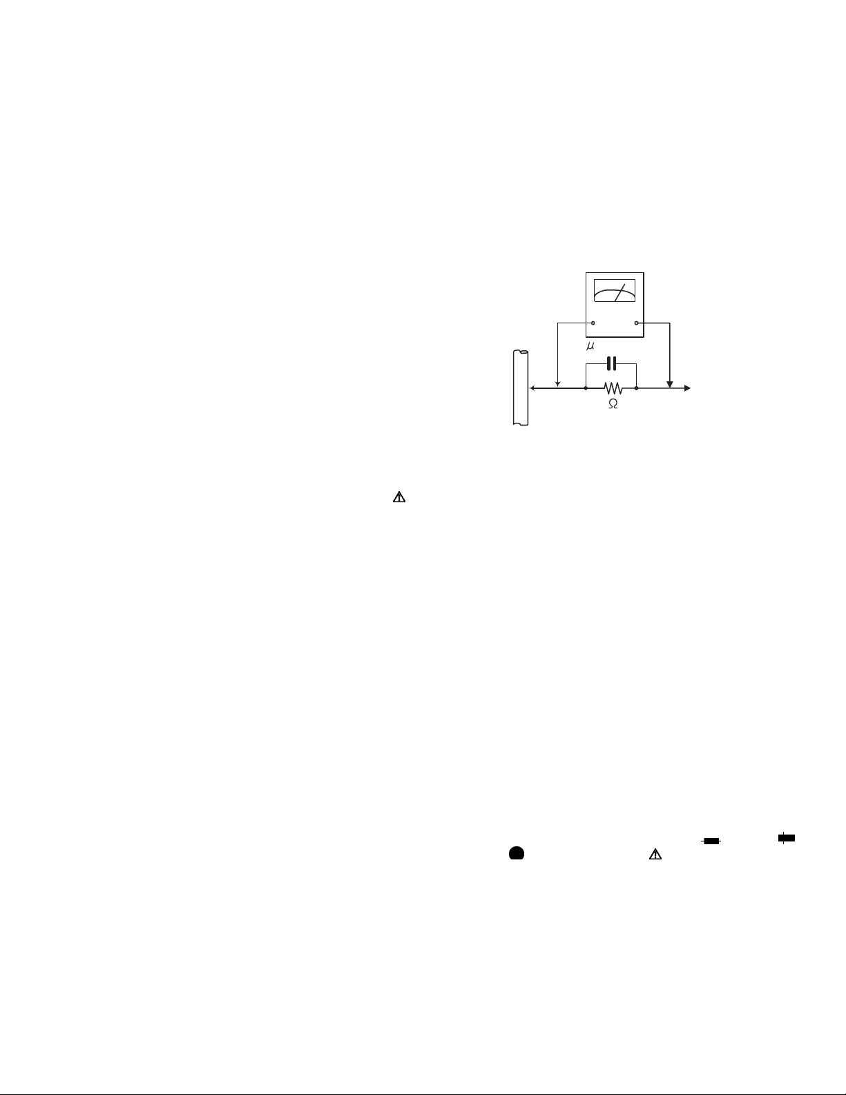
(5) Leakage shock hazard testing
After reassembling the product, always perform an isolation check on the exposed metal parts of the product (antenna terminals, knobs, metal cabinet, screw heads,
headphone jack, control shafts, etc.) to be sure the product
is safe to operate without danger of electrical shock.Do not
use a line isolation transformer during this check.
• Plug the AC line cord directly into the AC outlet. Using a
"Leakage Current Tester", measure the leakage current
from each exposed metal parts of the cabinet, particularly any exposed metal part having a return path to the
chassis, to a known good earth ground. Any leakage current must not exceed 0.5mA AC (r.m.s.).
• Alternate check method
Plug the AC line cord directly into the AC outlet. Use an
AC voltmeter having, 1,000Ω per volt or more sensitivity
in the following manner. Connect a 1,500Ω 10W resistor
paralleled by a 0.15µF AC-type capacitor between an ex-
posed metal part and a known good earth ground.
Measure the AC voltage across the resistor with the AC
voltmeter.
Move the resistor connection to each exposed metal
part, particularly any exposed metal part having a return
path to the chassis, and measure the AC voltage across
the resistor. Now, reverse the plug in the AC outlet and
repeat each measurement. Voltage measured any must
not exceed 0.75 V AC (r.m.s.). This corresponds to 0.5
mA AC (r.m.s.).
AC VOLTMETER
(Having 1000
ohms/volts,
or more sensitivity)
0.15 F AC TYPE
Place this
probe on
1500 10W
Good earth ground
1.2 Warning
(1) This equipment has been designed and manufactured to
meet international safety standards.
(2) It is the legal responsibility of the repairer to ensure that
these safety standards are maintained.
(3) Repairs must be made in accordance with the relevant
safety standards.
(4) It is essential that safety critical components are replaced
by approved parts.
(5) If mains voltage selector is provided, check setting for local
voltage.
1.3 Caution
Burrs formed during molding may be left over on some parts
of the chassis.
Therefore, pay attention to such burrs in the case of preforming repair of this system.
1.4 Critical parts for safety
In regard with component parts appearing on the silk-screen
printed side (parts side) of the PWB diagrams, the parts that are
printed over with black such as the resistor ( ), diode ( )
and ICP ( ) or identified by the " " mark nearby are critical
for safety. When replacing them, be sure to use the parts of the
same type and rating as specified by the manufacturer.
(This regulation dose not Except the J and C version)
each exposed
metal part.
(No.MA467<Rev.002>)1-5
Page 6
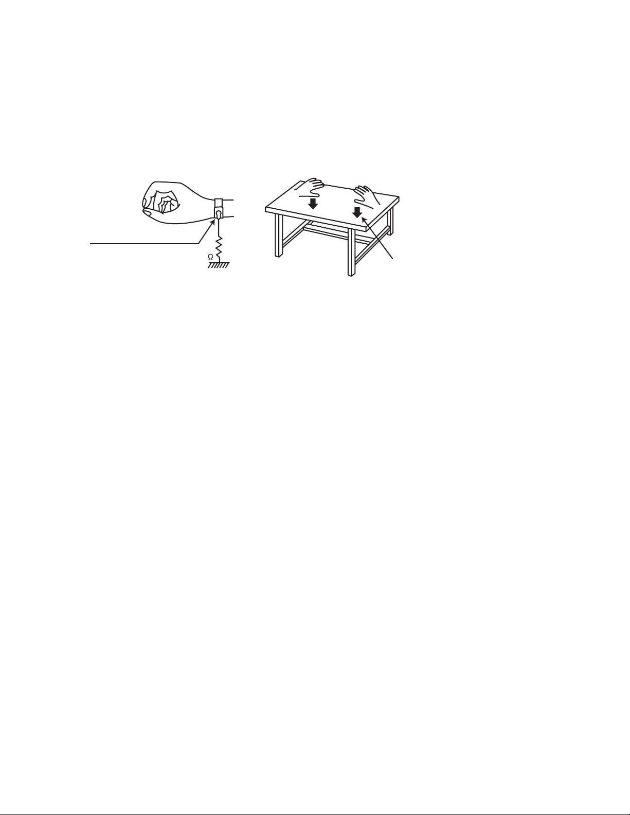
1.5 Preventing static electricity
Electrostatic discharge (ESD), which occurs when static electricity stored in the body, fabric, etc. is discharged, can destroy the laser
diode in the traverse unit (optical pickup). Take care to prevent this when performing repairs.
1.5.1 Grounding to prevent damage by static electricity
Static electricity in the work area can destroy the optical pickup (laser diode) in devices such as laser products.
Be careful to use proper grounding in the area where repairs are being performed.
(1) Ground the workbench
Ground the workbench by laying conductive material (such as a conductive sheet) or an iron plate over it before placing the
traverse unit (optical pickup) on it.
(2) Ground yourself
Use an anti-static wrist strap to release any static electricity built up in your body.
(caption)
Anti-static wrist strap
1M
Conductive material
(conductive sheet) or iron palate
(3) Handling the optical pickup
• In order to maintain quality during transport and before installation, both sides of the laser diode on the replacement optical
pickup are shorted. After replacement, return the shorted parts to their original condition.
(Refer to the text.)
• Do not use a tester to check the condition of the laser diode in the optical pickup. The tester's internal power source can easily
destroy the laser diode.
1.6 Handling the traverse unit (optical pickup)
(1) Do not subject the traverse unit (optical pickup) to strong shocks, as it is a sensitive, complex unit.
(2) Cut off the shorted part of the flexible cable using nippers, etc. after replacing the optical pickup. For specific details, refer to the
replacement procedure in the text. Remove the anti-static pin when replacing the traverse unit. Be careful not to take too long a
time when attaching it to the connector.
(3) Handle the flexible cable carefully as it may break when subjected to strong force.
(4) I t is not possible to adjust the semi-fixed resistor that adjusts the laser power. Do not turn it.
1-6 (No.MA467<Rev.002>)
Page 7
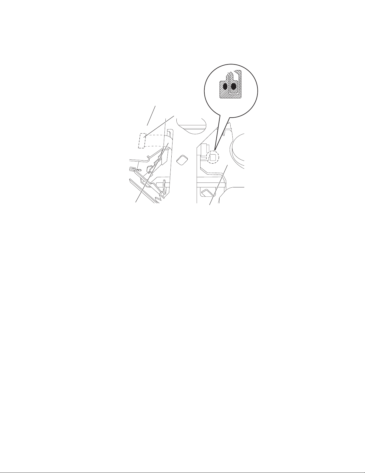
1.7 Attention when traverse unit is decomposed
*Please refer to "Disassembly method" in the text for the pickup unit.
• Apply solder to the short land sections before the card wire is disconnected from the connector on the servo board. (If the card wire
is disconnected without applying solder, the pickup may be destroyed by static electricity.)
• In the assembly, be sure to remove solder from the short land sections after connecting the card wire.
Mechanism control board
CN102
Flexible wire
Short land section
Pickup
(No.MA467<Rev.002>)1-7
Page 8
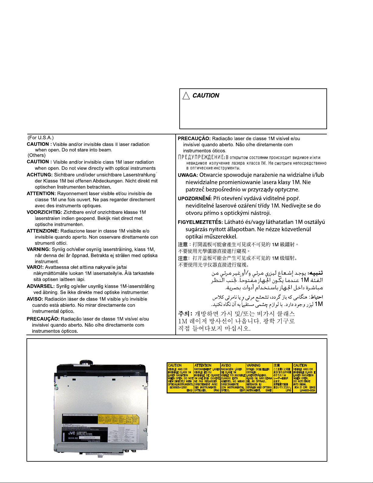
1.8 Important for laser products
1.CLASS 1 LASER PRODUCT
2.CAUTION :
(For U.S.A.) Visible and/or invisible class II laser radiation
when open. Do not stare into beam.
(Others) Visible and/or invisible class 1M laser radiation
when open. Do not view directly with optical instruments.
3.CAUTION : Visible and/or invisible laser radiation when
open and inter lock failed or defeated. Avoid direct
exposure to beam.
4.CAUTION : This laser product uses visible and/or invisible
laser radiation and is equipped with safety switches which
prevent emission of radiation when the drawer is open and
the safety interlocks have failed or are defeated. It is
dangerous to defeat the safety switches.
5.CAUTION : If safety switches malfunction, the laser is able
to function.
6.CAUTION : Use of controls, adjustments or performance of
procedures other than those specified here in may result in
hazardous radiation exposure.
!
Please use enough caution not to
see the beam directly or touch it
in case of an adjustment or operation
check.
REPRODUCTION AND POSITION OF LABELS and PRINT
WARNING LABEL and PRINT
1-8 (No.MA467<Rev.002>)
Page 9
SECTION 2
SPECIFIC SERVICE INSTRUCTIONS
This service manual does not describe SPECIFIC SERVICE INSTRUCTIONS.
SECTION 3
DISASSEMBLY
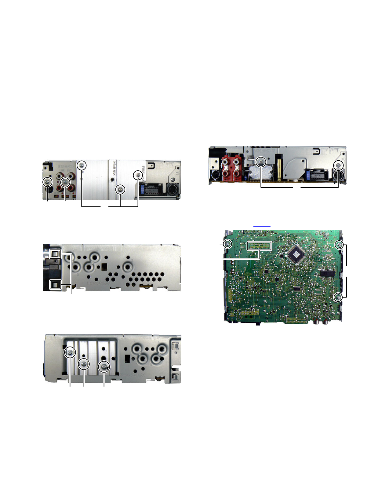
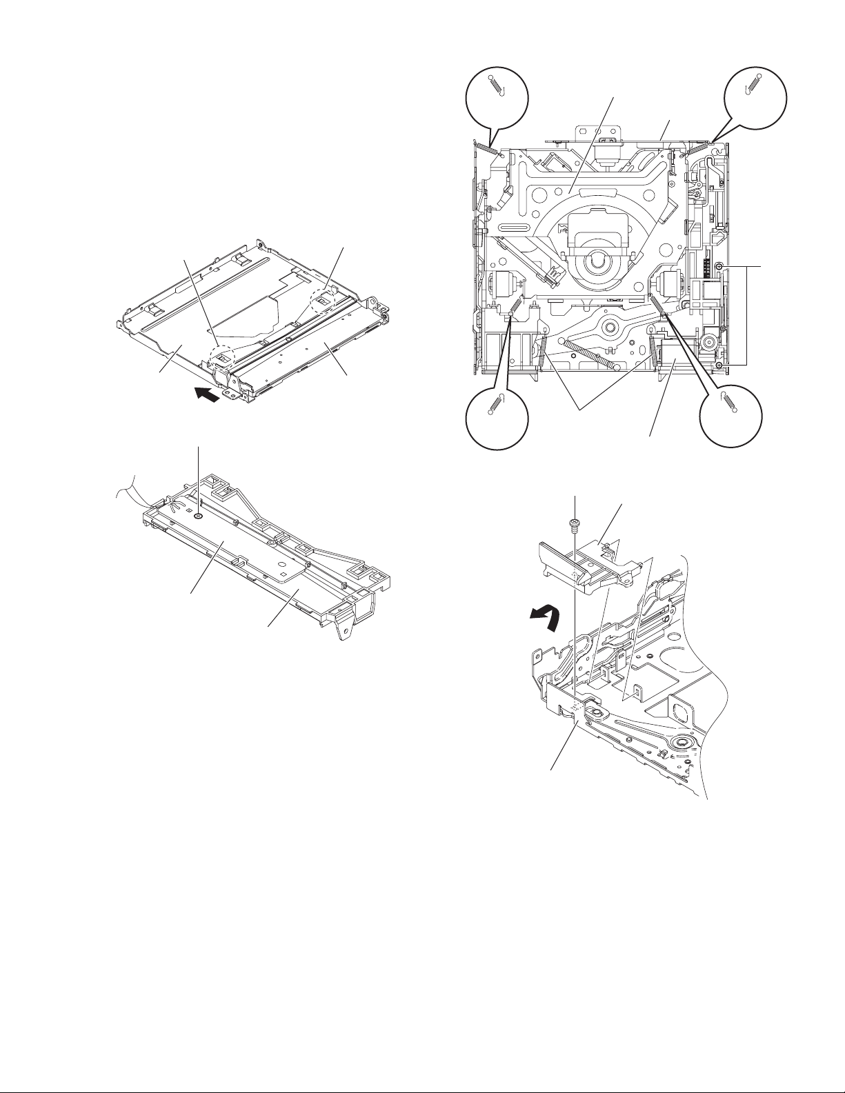
3.1 Main body (Used figure were KD-R610U)
3.1.1 Removing the Bottom chassis (See Fig.1)
(1) Remove the three screws A attaching the Heat sink.
(2) Remove the one screw B and one screw C attaching the
Bottom chassis.
(2) Remove the two screw F attaching the Top chassis. (See
Fig.4)
F
Fig.4
ACB
Fig.1
3.1.2 Removing the Front chassis (See Fig.2)
(1) Disengage four hooks a engaged both side of the Front
chassis.
(3) Remove the three screws G attaching the Main board.
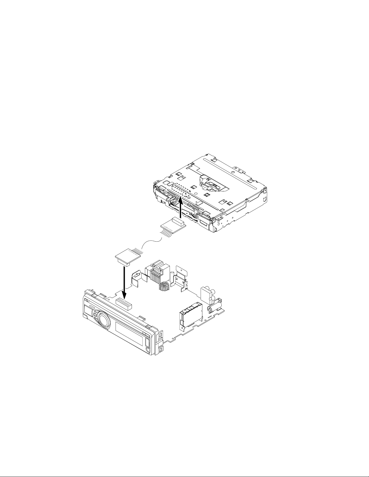
(See Fig.5)
(4) Disconnect the B-B connector connected CD mechanism
and Main board CN501
of the Main board. (See Fig.5)
G
hook
a
Fig.2
3.1.3 Removing the Main board (See Fig.3, 4, 5)
(1) Remove the two screws D and one screw E attaching the
Side plate. (See Fig.3)
DE D
Fig.3
CN501
G
Fig.5
(No.MA467<Rev.002>)1-9
Page 10
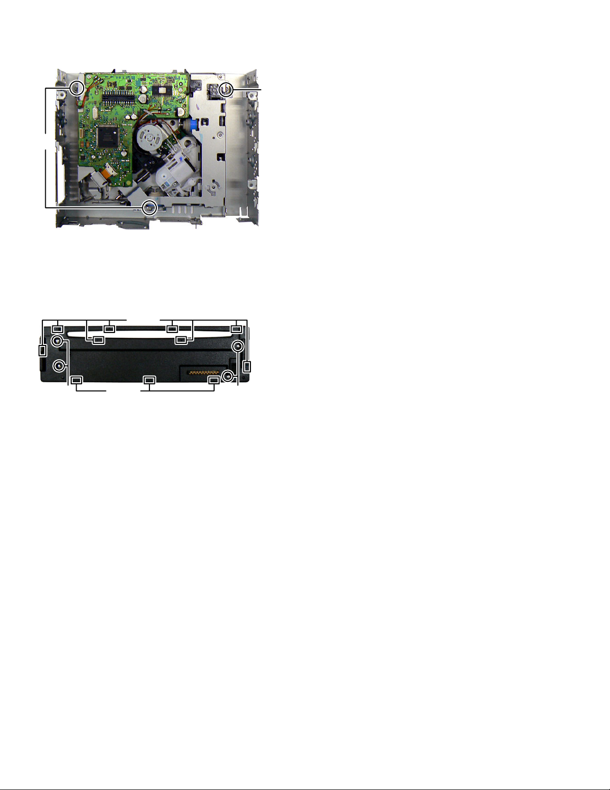
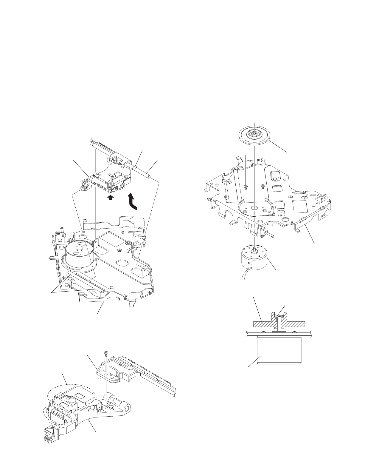
3.1.4 Removing the CD mechanism (See Fig.6)
H
(1) Remove the three screws H attaching the CD mechanism.
H
Fig.6
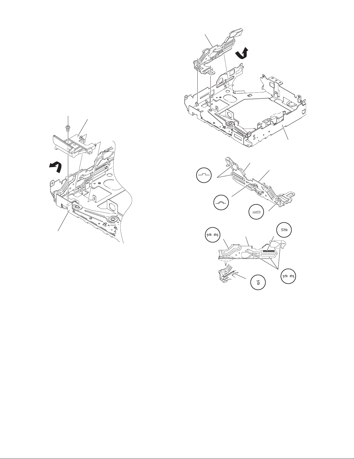
3.1.5 Removing the Switch board (See Fig.7)
(1) Remove the Volume knob.ZZ
(2) Remove the four screws J attaching the Rear cover.
(3) Disengage eleven hooks b engaged Rear cover.
hook
b
hook
b
JJ
Fig.7
1-10 (No.MA467<Rev.002>)
Page 11
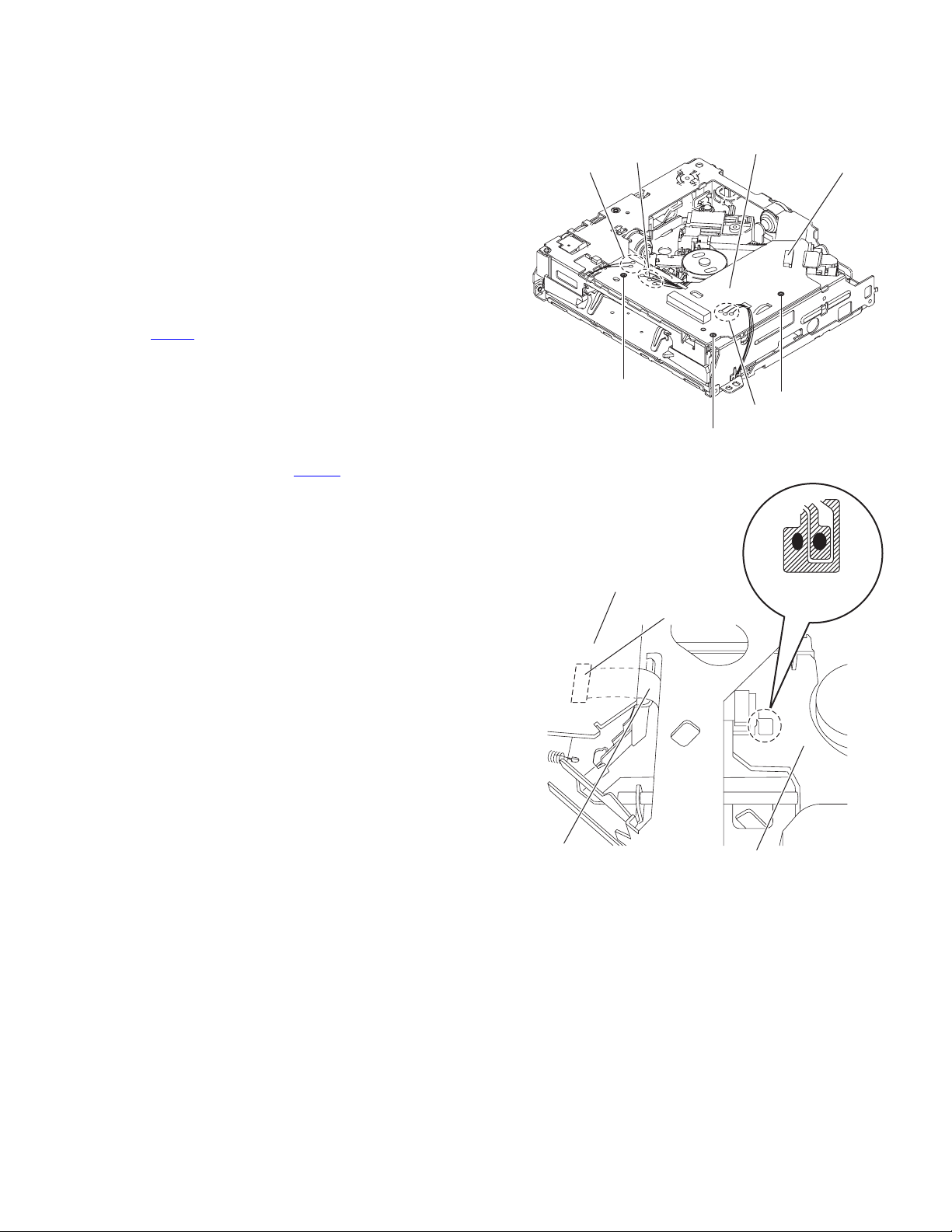
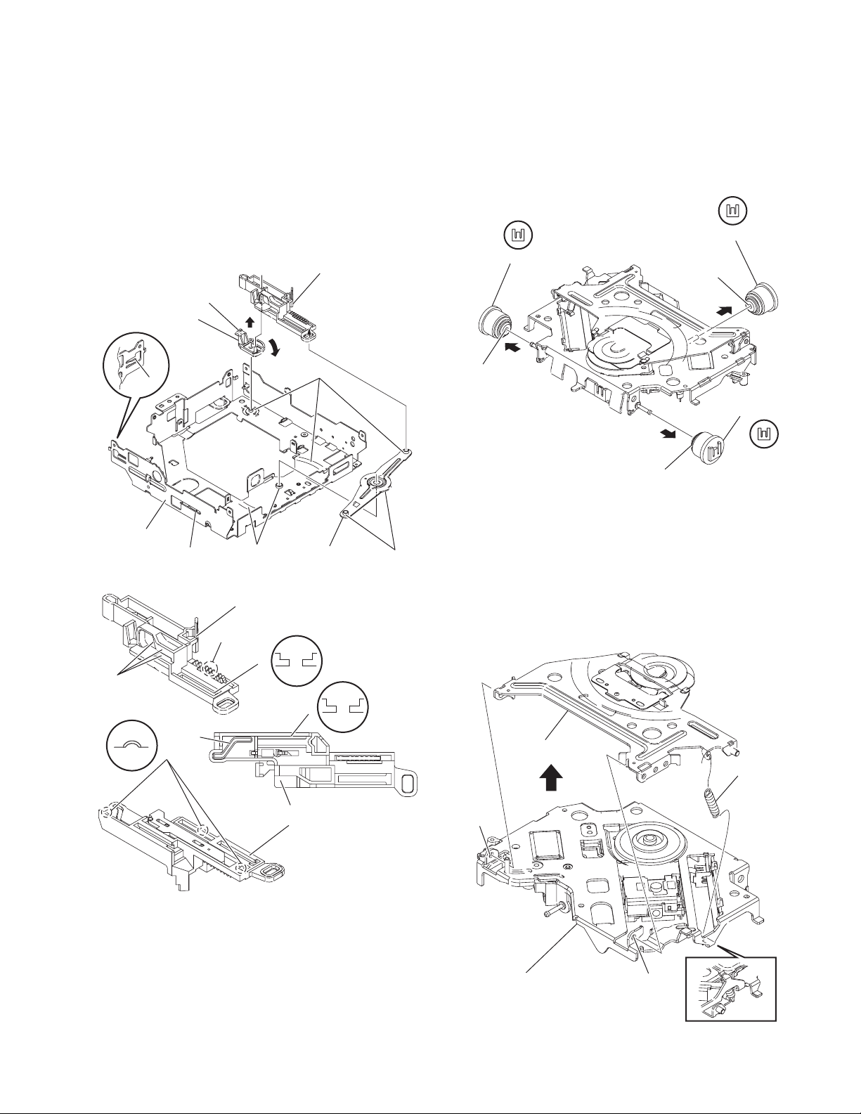
3.2 CD MECHANISM assembly section
• Remove the CD MECHANISM assembly from the main body.
Removing the MECHANISM CONTROL BOARD
3.2.1
1
assembly (See Fig.
(1)
From the bottom side of CD MECHANISM assembly,
remove the solders from the soldered sections (
c
) on the MECHANISM CONTROL BOARD assembly.
(See Fig.
(2) Remove the three screws A attaching the MECHANISM
CONTROL BOARD assembly. (See Fig.1.)
(3) Solder the short land sections on the pickup. (See Fig.2.)
Caution:
• Solder the short land sections on the pickup before
•
1
.)
disconnecting the flexible wire from the connector
on the MECHANISM CONTROL BOARD as-
CN102
sembly.
If the card wire is disconnected without attaching
solder, the pickup may be destroyed by static
electricity. (See Fig.2.)
When attaching the MECHANISM CONTROL
BOARD assembly, remove the solders from the
short land sections after connecting the flexible
wire to the connector CN102
CONTROL BOARD assembly.
and 2)
a, b
and
on the MECHANISM
Mechanism
a
b
control board
CN102
A
A
c
A
Fig.1
Mechanism control board
CN102
Flexible wire
Short land section
Pickup
Fig.2
(No.MA467<Rev.002>)1-11
Page 12
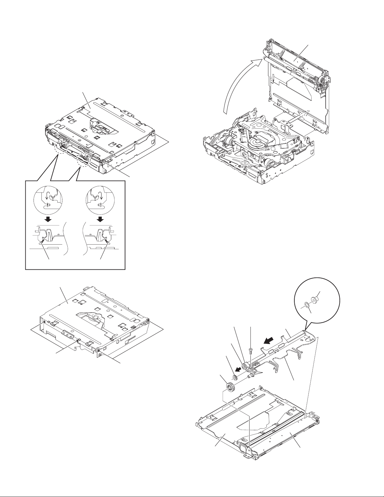
3.2.2 Removing the top cover (See Fig.3 to 5)
• Remove the MECHANISM CONTROL BOARD assembly.
(1) From the front side of the CD MECHANISM assembly,
change the hook position of the two roller springs. (See
Fig.3.)
(2) From the side of the CD MECHANISM assembly, remove
the six screws B attaching the top cover. (See Fig.3 and 4.)
(3) Take out the top cover in an upward direction. (See Fig.5.)
Top cover
B
Roller spring Roller spring
Fig.3
Top cover
Top cover
Fig.5
3.2.3 Removing the roller (See Fig.6)
• Remove the MECHANISM CONTROL BOARD assembly and
top cover.
(1) From the bottom side of the top cover, remove the screw C
attaching the gear holder.
(2) Remove the R.holder assembly from disc plate, and then
take out the roller from R.holder assembly in the direction
of the arrow.
Reference:
When attaching the R.ACT gear (2) and R.ACT gear (3),
apply grease to the section d of R.holder assembly.
Roller coller
B
1-12 (No.MA467<Rev.002>)
Fig.4
B
Gear holder
Roller gear
R.ACT gear(3)
R.ACT gear(2)
Top cover
C
d
R.holder assembly
Fig.6
Washer
Roller
Disc plate
Page 13
3.2.4 Removing the PHOTO BOARD assembly (See Fig.7
and 8)
• Remove the MECHANISM CONTROL BOARD assembly and
top cover.
From the bottom side of the top cover, release the
(1)
projection
7
Fig.
(2) Take out the disc plate in the direction of the arrow. (See
Fig.7.)
(3) From the reverse side of the disc plate, remove the screw
D attaching the PHOTO BOARD assembly. (See Fig.8.)
e
from the notch of the disc plate. (See
.)
e
e
SUS
spring
Mechanism section
Mecha frame
SUS
spring
E
Top cover
Fig.7
Disc plate
D
Photo board
Disc plate
Fig.8
3.2.5 Removing the mechanism section (See Fig.9 and 10)
• Remove the MECHANISM CONTROL BOARD assembly and
top cover.
(1)
From the top side of the CD MECHANISM assembly,
remove the two screws
assembly. (See Fig.
(2) Remove the two roller springs on the top side of the mecha
frame. (See Fig.9.)
(3) Remove the four SUS springs on the top side of the mecha
frame. (See Fig.9.)
(4) Remove the link spring on the top side of the mecha frame.
(See Fig.10.)
(5) Release section f of the three dampers from the mecha
frame. (See Fig.10.)
Reference:
When attaching the roller spring and SUS spring, keep
direction before remove.
Move the slide cam (R) assembly in the direction of the
(6)
arrow, and then take out the mechanism section in an
upward direction. (See Fig.
Reference:
When attaching the mechanism section, apply grease to
the section g. (See Fig.10.)
E
attaching the loading motor
9
.)
10.)
SUS
spring
Roller spring
Loading motor assembly
Fig.9
F
Cam cover
Mecha frame
Fig.10
SUS
spring
(No.MA467<Rev.002>)1-13
Page 14
3.2.6 Removing the slide cam (L) (See Fig.11 to 13)
• Remove the MECHANISM CONTROL BOARD assembly, top
cover and mechanism section.
(1) From the top side of the mecha frame, remove the screw F
attaching the cam cover. (See Fig.11.)
Take out the cam cover from mecha frame in an upward
(2)
11
F
.)
Cam cover
direction. (See Fig.
(3) Take out the slide cam (L) in the direction of the arrow.
(See Fig.12.)
Reference:
When attaching the slide cam (L), apply grease to the
section h. (See Fig.13.)
Slide cam(L)
Mecha frame
Fig.12
h
Slide cam(L)
h
Mecha frame
Fig.11
h
h
Slide cam(L)
h
Fig.13
h
h
h
1-14 (No.MA467<Rev.002>)
Page 15
3.2.7 Removing the F.lock lever and slide cam (R) (See
Fig.14 and 15)
• Remove the MECHANISM CONTROL BOARD assembly, top
cover and mechanism section.
(1) From the top side of the mecha frame, take out the slide
cam (R) assembly in an upward direction. (See Fig.14.)
(2) Rotate the F.lock lever in the direction of the arrow 1, and
then take out the direction of the arrow 2. (See Fig.14.)
Reference:
When attaching the slide cam (R) assembly, the f.lock
lever and the link arm apply grease to the section
14
(See Fig.
and 15.)
h
Slide cam(R) assembly
h
F.lock lever
2
1
h
h
3.2.8 Removing the damper (See Fig.16)
• Remove the MECHANISM CONTROL BOARD assembly, top
cover and mechanism section.
From the mechanism section, pull out the three dampers in the
direction of the arrow.
Reference:
Before inserting the shaft to the dampers, apply IPA to the
pocket j of damper.
.
Damper (Gray)
Damper (Brown)
j
j
Damper (Brown)
j
Fig.16
Mecha frame
h
h
h
h
Fig.14
Link arm
Slide cam(R) assembly
h
h
h
Slide cam(R) assembly
Fig.15
3.2.9 Removing the clamper assembly (See Fig.17)
• Remove the MECHANISM CONTROL BOARD assembly, top
h
cover and mechanism section.
(1) From the top side of the mechanism section, release the
clamper spring.
(2) Move the clamper assembly in the direction of the arrow,
and then release the joints (k and m).
Take out the clamper assembly from the T.M chassis
(3)
assembly.
h
Clamper assembly
Clamper spring
k
T.M. chassis assembly
m
Fig.17
(No.MA467<Rev.002>)1-15
Page 16
3.2.10 Removing the feed motor (See Fig.18 and 19)
r
• Remove the MECHANISM CONTROL BOARD assembly, top
cover, mechanism section and clamper assembly.
(1) From the bottom side of the T.M chassis assembly, remove
the two screws G attaching the feed motor assembly. (See
Fig.18.)
Remove the two screws H attaching the feed motor to
(2)
19
f.motor holder. (See Fig.
Reference:
When attaching the f. wheel gear, trigger arm and feed
motor, apply grease to the sections (n, p and q). (See
Fig.18 and 19.)
.)
Feed motor
F.worm gear
q
Comp. spring
H
3.2.11 Removing the SWITCH BOARD assembly (See
Fig.18)
• Remove the MECHANISM CONTROL BOARD assembly, top
cover, mechanism section, clamper assembly and feed motor
assembly.
From the bottom side of the T.M chassis assembly, take out
the SWITCH BOARD assembly in an upward direction from
T.M chassis assembly.
G
Feed motor assembly
Switch board
p
n
F.wheel gear
Trigger arm
F.motor holder
Fig.19
3.2.12 Removing the loading motor (See Fig.20)
• Remove the MECHANISM CONTROL BOARD assembly, top
cover, mechanism section and clamper assembly.
(1) From the right side of the L.M base assembly, remove the
two screws J attaching the loading motor.
(2) Take out the loading motor in the direction of the arrow
from the L.M base assembly.
Reference:
When attaching the loading motor, apply grease to the
section r.
J
r
L.M. base assembly
Fig.20
L.worm gear
Loading moto
T.M. chassis assembly
1-16 (No.MA467<Rev.002>)
Fig.18
Page 17
3.2.13 Removing the pickup assembly (See Fig.21 to 22)
• Remove the MECHANISM CONTROL BOARD assembly, top
cover, mechanism section, clamper assembly and feed motor
assembly.
Caution:
• Do not touch section u on the pickup assembly. (See Fig.21
and 22.)
(1) From the bottom side of the T.M chassis assembly, move
the pickup assembly in the direction of the arrow from the
T.M chassis assembly. (See Fig.21.)
(2) Pull out the main shaft. (See Fig.21.)
(3) Remove the screw K attaching the pickup to the rack plate.
(See Fig.22.)
Reference:
When attaching the loading motor, apply grease to the
sections s and t. (See Fig.21.)
3.2.14 Removing the spindle motor (See Fig.23 and 24)
Remove the MECHANISM CONTROL BOARD assembly,
•
top cover, mechanism section, clamper assembly, feed motor
assembly and pickup assembly.
(1) From the top side of the T.M chassis assembly, remove the
CD T.table assembly from the spindle motor. (See Fig.23.)
(2) Remove the two screws L attaching the spindle motor.
(See Fig.23.)
(3) Take out the spindle motor from the bottom side of the T.M
chassis assembly. (See Fig.23.)
Reference:
When attaching the CD T.table assembly to the spindle
motor shaft, apply loctite 460 to inside the CD T.table
assembly. (See Fig.24.)
Pick up assembly
s
T.M. chassis assembly
u
Fig.21
t
Main shaft
LL
Spindle motor
Fig.23
CD T.table assembly
CD T.table assembly
T.M.chassis assembly
Loctite
u
K
Rack plate
Spindle motor
Fig.24
Pick up
Fig.22
(No.MA467<Rev.002>)1-17
Page 18
SECTION 4
ADJUSTMENT
4.1 Test instruments required for adjustment
(1) Digital oscilloscope (100MHz)
(2) Digital tester
(3) Test Disc
(4) Extension cable : EXTCD004-28P
4.2 Standard measuring conditions
Power supply voltage DC14.4V(10.5 to 16V)
Load impedance 20K ohm (2 Speakers connection)
Output Level Line out 2.5V (Vol. MAX)
4.5 How to connect the extension cable for adjusting
Caution:
Be sure to attach the heat sink and rear bracket onto the power amplifier IC and regulator IC respectively, before supply the power.
If voltage is applied without attaching these parts, the power amplifier IC and regulator IC will be destroyed by heat.
Extension cable
EXTCD004-28P
4.3 Standard volume position
Balance and Bass &Treble volume : lndication"0"
Loudness : OFF
4.4 Dummy load
Exclusive dummy load should be used for AM,and FM.
For FM dummy load, there is a loss of 6dB between SSG output
and antenna input.
The loss of 6dB need not be considered sincedirect reading of
figures are applied in this working standard.
1-18 (No.MA467<Rev.002>)
Page 19
4.6 SERVICE MODE
Operating key: [MENU] → [DOWN] (3 sec)
Navigation key : Press [SEL] in any main display item to select that option.
Volume Knob Turn: forward and backward selection
INT ALL Initialize all data to factory shipment state.
Note : A disc is inserted, and it is displayed only at the time of CD function.
RUNNING MODE 1 CD6 module running mode 1 (Only factory use)
MODE 2 CD6 module running mode 2 (Only factory use)
CHECK MODE
CD ERROR
NORMAL PLAY Disc operation & playback. (playback from starting position)
CURENT ##** Laser Electric Current Value
##: Initial value **: Current value
JITTER #### Jitter Value
Note: Pressing "FF" or "REW" key to switch between
current value and jitter value display.
OUT TRK OFF Tracking off at CD outermost lap.
INN TRK OFF Tracking off at CD innermost lap.
CD LASER ON CD Laser Illumination and electric current.
CURENT ##** Laser Electric Current Value
##: Initial value **: Current value
JITTER #### Jitter Value
Note: Pressing "FF" or "REW" key to switch between
current value and jitter value display.
STOP Disc stop, LD(Laser) OFF
Display the CD Error past record stored in EEPROM.
TOTAL-****: Total error count
E#xxyyyy : Latest 3 errors recorded. #: countor xx: error code yyyy: detailed error code
0#xxyyyy : The first 5 errors recorded. #: countor xx: error code yyyy: detailed error code
Note: Shifting among the above items is done by using "FF" or "REW" key.
CLR CDERROR
TSUBUYAKI
DC OK
Clear CD Error history from EEPROM.
Only engineer use
DC offset error information
*See " DC offset error information " for details.
(No.MA467<Rev.002>)1-19
Page 20

4.7 DC OFFSET ERROR INFORMATION
4.7.1 Display indication
DC OK
DC ERROR
VOL
push
BACK
DC 1 ERROR
VOL
knob
VOL
push
BACK
CLR DC1 VOL push to confirmDC 1 OK
DC 2 X
VOL
push
CLR DC2 VOL push to confirm
BACK
4.7.2 Error content confirmation.
Whether it turns on power and the "PROTECT" display appears are confirmed.
(1) When the "PROTECT" display appears.
The content of the DC offset error is confirmed in the Service mode.
* Because it takes DC offset protection, the following is displayed.
"DC ERROR"
(1-1) When "DC1 ERROR" is displayed. (DC ERROR1)
•Forecast cause
It comes in contact with improper connection or GND of the speaker wiring.
It is confirmed that there is no improper connection of the speaker wiring and pushes reset.
•When "PROTECT" is not displayed, it is unquestionable.
The error data of EEPROM, it deletes it. (CLR DC1)
•When "PROTECT" is still displayed.
The DC offset has been generated by the reasons other than the improper connection.
Forecast cause: Power AMP is broken.
After parts are exchanged, reset is confirmed pushing again.
(1-2) When "DC2 X" is displayed. (DC ERROR2)
* As for X, the detected number is displayed. (0-4)
* When X is 0, it is unquestionable because the DC offset has never been detected.
When leak of capacitor is detected, it is displayed.
It is confirmed that there is no problem in the capacitor and deletes the error data of EEPROM. (CLR DC2)
It is confirmed that reset is pushed and "PROTECT" is not displayed.
After above-mentioned (1-1) and (1-2) are executed, the conect of the DC offset error is confirmed in the Service mode.
If the part displayed as "DC ERROR" becomes "DC OK", it is unquestionable.
(2) When the "PROTECT" display doesn't appear.
The content of the DC offset error is confirmed in the Service mode.
(2-1) When "DC OK" is displayed, it is unquestionable because the DC offset has not been detected in the past.
(2-2) When "DC ERROR" is displayed, the confirmation similar to (1-1) and (1-2) is done because there is a history that detected
the DC offset error in the past.
1-20 (No.MA467<Rev.002>)
Page 21

4.8 TUNER SERVICE MODE
Key operation (FM and AM mode)
Enter service mode: [SEL] → [MENU] (3 sec)
Exit service mode: press [ENTER] (SEL) key.
Go to next item: press [DISP] key
Back to previous item: press [BACK] key
VER=#*** MICON version display
# indicates destination: J=USA, U=OTHERS (eg. ASIA), R=EUROPE, E=EASTERN EUROPE
*** indicates version No.
CD6V#### CD module version display.
######## Tuner device and version identification display
Display :TOM V3 for TOMIC V3 tuner.
Display: ATOM V5 for ATOMIC V5 tuner.
TINJ= ## Tuner injection indicator
"##" indicates current tuner injection.
FOR RDS ONLY
PI =#### PI display of receiving station, "####" indicates PI code.
PTY=## PTY display of receiving station (00~29), "##" indicates PTY code.
TP=#TA=* TP, TA display of receiving station
"#" indicates TP ON/OFF: 1=ON; 0=OFF;
"*" indicates TA ON/OFF: 1=ON; 0=OFF.
MS=#DI=* M/S, DI display of receiving station
"#" indicates M/S ON/OFF: 1=ON; 0=OFF;
"*" indicates DI ON/OFF: 1=ON; 0=OFF.
AF=#### Display the contents of AF memory (by scrolling) "####" indicate AF frequencies.
LEV= ##H Field strength indicator.
U&W= ##H Adjacent and Multi path noise level indicator.
IFC= ##H IF COUNTER result indicator.
IFBW= # FM IF filter bandwidth indicator.
RFAGC=## FM RF AGC resulting attenuation.
IFAGC=## FM IF AGC resulting attenuation.
##** CLOCK display of receiving station (Original DISP key operation)
######## FOR RDS ONLY
PS NAME display of receiving station (Original DISP key operation)
##### FREQUENCY display of receiving station (Original DISP key operation)
(No.MA467<Rev.002>)1-21
Page 22

4.9 ERROR CODE
4.9.1 Mechanical Error Detail Codes
Condition Details Error code Detailed code
LOADING Error Error without SW change in LOAD when time-out is done
B1 time out When there is no change in the state of the switch from the state
with DISC forward.
C1 time out When there is no change in the state of the switch from the state
that DISC is drawn in a half.
B2 time out When there is no change in the state of the switch from the state
that DISC is in the interior.
EJECT Error Error without SW change in EJECT when time-out is done.
B1 time out When there is no change in the state of the switch from the state
that DISC is in the interior.
C2 time out When there is no change in the state of the switch from the state
that DISC is drawn in a half.
B2 time out When there is no change in the state of the switch in EJECT from
initial LOAD ERROR.
FORCE EJECT Error Transition to Force EJECT waiting or Force EJECT transition from
error Error by abnormal SW.
E1 FORCE EJECT ERROR When detect abnormal SW from the state of NO DISC 01 0041
E2 FORCE EJECT ERROR When detect abnormal SW from the state with DISC forward in
LOAD.
E3 FORCE EJECT ERROR When detect abnormal SW from the initial state. 01 0043
E5 FORCE EJECT ERROR When detect abnormal SW from the state that half DISC is drawn
in LOAD and EJECT.
E7 FORCE EJECT ERROR When detect abnormal SW from the atate that DISC is in the inte-
rior in LOAD and EJECT.
E8 FORCE EJECT ERROR When receive Force EJECT key after it makes an error from Force
EJECT.
E9 FORCE EJECT ERROR When receive Force EJECT key after it makes an error from LOAD
error or EJECT error.
Error in Running mode
Case 1 When DISC was extracted or fall in EJECT END and EJECT
START.
Case 2 When DISC is pushed in EJECT END. 09 0032
09 0011
09 0012
09 0015
01 0023
01 0026
01 0027
01 0042
01 0045
01 0047
01 0048
01 0049
09 0031
4.9.2 Disc error code
Condition Details Error code Detailed code
TOC READING Error When it hasn't completed CD TOC reading. 84 0059
1'st track access Error It doesn't end even if the first track access passes 30sec after the
TOC reading ends in the running mode.
Last track access Error It doesn't end even if the last track access passes 30sec after the
first track ends in the running mode.
NODISC judgement It be judged NODISC. 80 0090
NO DISC with start failure Not possible to start. 80 0091
Stopped with no playback When it was stopped in playback in the running mode. 80 0093
Logical format NG Analysis of logical format is impossible or it does not correspond
to logical formats.
1-22 (No.MA467<Rev.002>)
80 0060
80 0061
80 0094
Page 23

SECTION 5
TROUBLESHOOTING
16 PIN CORD DIAGRAM (For KD-A615/KD-R610/KD-R618)
Black
8
7
GN/BK
6
VI/BK GY/BK
VI GY
5
NC
WHGN
WH/BK
NC
9
10
11
12
134
BK
RD
BL
WH
VI
Red
Blue
White
Violet
GN
GY
YL
Green
Gray
OrangeOR
Yellow
BK
1
YL
16
OR/WH
15
RD
2
GN
8
GN/BK
7
VI
5
3
2
1
BL/WH
RD
BK
NC
OR/WH
YL
14
15
16
VI/BK
6
WH
9
WH/BK
10
GY
12
GY/BK
11
BL/WH
3
(No.MA467<Rev.002>)1-23
Page 24

16 PIN CORD DIAGRAM (For KD-R611/KD-R612)
2
16
15
1
3
13
8
7
6
5
4
3
2
1
RD1
YL1
OR/WH
BK
BL/WH
BR
GN
GN/BK
VI/BK
VI
NC
BL/WH
RD
BK
WH
WH/BK
GY/BK
GY
BR
NC
OR/WH
YL
10
11
12
13
14
15
16
9
Black
BK
RD
BL
WH
VI
Red
Blue
White
Violet
GN
GY Gray
BR
OR
YL
RD2
Green
Brown
Orange
Yellow
1
3
5
7
RD3
YL2
NC
NC
BL/WH
RD3
7
4
6
8
5
2
BR
YL2
OR/WH
BK
2
4
6
8
8
7
5
6
9
10
12
11
GN
GN/BK
VI
VI/BK
WH
WH/BK
GY
GY/BK
7
8
1
2
5
6
3
4
VI/BK
VI
1
GY
3
WH
5
GN
7
GY/BK
WH/BK
GN/BK
2
4
6
8
1-24 (No.MA467<Rev.002>)
Page 25

16 PIN CORD DIAGRAM (For KD-R616)
8
7
GN/BK
6
VI/BK GY/BK
5
VI GY
NC
WHGN
WH/BK
NC
9
10
11
12
134
BK
RD
BL
WH
VI
Black
Red
Blue
White
Violet
GN
GY
YL
Green
Gray
OrangeOR
Yellow
BK
1
YL
16
BL
4
BL/WH
3
RD
2
OR/WH
15
3
2
1
BL/WH
RD
BK
NC
OR/WH
YL
14
15
16
8
7
5
6
9
10
12
11
GN
GN/BK
VI
VI/BK
WH
WH/BK
GY
GY/BK
(No.MA467<Rev.002>)1-25
Page 26

Victor Company of Japan, Limited
Mobile Entertainment Division 10-1,1chome,Ohwatari-machi,Maebashi-city,371-8543,Japan
(No.MA467<Rev.002>)
Printed in Japan
VSE
Page 27

REVISION INFORMATION
CD RECEIVER
KD-A615J, KD-R610J, KD-R611E, KD-R611EU,
KD-R611EY, KD-R612E, KD-R616U, KD-R616UH,
KD-R616UN, KD-R618J
■ OVERVIEW
Add KD-R612E.
■ DETAILS
COVER SECTION
Title Line No.MA467<Rev.001> No.MA467<Rev.002> Description
Revision Rev.001 Rev.002
Issue Date 2010/02 2010/06
Model No. KD-A615J, KD-R610J, KD-R611E,
Cover Illustration ILLUSTRATION(ma467_0001.png) ILLUSTRATION(ma467_0001.png)
SPECIFICATION 104
KD-R611EU, KD-R611EY, KD-R616U,
KD-R616UH, KD-R616UN, KD-R618J
KD-R611
KD-A615J, KD-R610J, KD-R611E, KD-R611EU,
KD-R611EY, KD-R612E, KD-R616U,
KD-R616UH, KD-R616UN, KD-R618J
KD-R611/KD-R612
PARTS LIST
MODEL No. LIST
Model No. No.MA467<Rev.002>
KD-A615J 01
KD-R610J 02
KD-R611E 03
KD-R611EU 04
General assembly [M1MM]
Symbol or
!
M1MM 23 ------------ GE33885-027A FINDER ASSY (Addition) 1 06
M1MM 31 ------------ GE33806-019A PHONE BACK BTN (Addition) 1 06
M1MM 40 ------------ GE10273-004A REAR COVER (Addition) 1 06
M1MM 47 ------------ GE34322-001A NAME PLATE (Addition) 1 06
<Rev.001> <Rev.002>
Part No.
Model No. No.MA467<Rev.002>
KD-R611EY 05
KD-R612E 06
KD-R616U 07
KD-R616UH 08
Part Name Description Qty Models
Model No. No.MA467<Rev.002>
KD-R616UN 09
KD-R618J 0A
COPYRIGHT © 2010 Victor Company of Japan, Limited
MA467-R002
2010/06
Page 28

Electrical parts list Main board [01]
Symbol or
!
01 C303 ------------ NCB21CK-474X-A C CAPACITOR (Addition) 1 06
01 C304 ------------ NCB21CK-474X-A C CAPACITOR (Addition) 1 06
01 C313 ------------ NCB21CK-474X-A C CAPACITOR (Addition) 1 06
01 C314 ------------ NCB21CK-474X-A C CAPACITOR (Addition) 1 06
01 C326 ------------ QERF1CM-106Z-E E CAPACITOR (Addition) 1 06
01 C327 ------------ NCB21AK-105X-A C CAPACITOR (Addition) 1 06
<Rev.001> <Rev.002>
Packing and accessories [M3MM]
Symbol or
!
M3MM A1 ------------ GET0640-001C INST BOOK (Addition) 1 06
M3MM A2 ------------ GET0640-002C INST BOOK (Addition) 1 06
M3MM A5 ------------ GET0640-008B INSTALL MANUAL (Addition) 1 06
M3MM A6 ------------ GET0640-009B INSTALL MANUAL (Addition) 1 06
M3MM A13 ------------ GE20204-320A TRIM PLATE (Addition) 1 06
M3MM P1 ------------ GE34323-002A CARTON (Addition) 1 06
M3MM P3 ------------ QPC03004315PG POLY BAG (Addition) 1 06
<Rev.001> <Rev.002>
Part No.
Part No.
Part Name Description Qty Models
Part Name Description Qty Models
Victor Company of Japan, Limited
Mobile Entertainment Division 10-1,1chome,Ohwatari-machi,Maebashi-city,371-8543,Japan
(MA467-R002)
Printed in Japan
No.MA467<Rev.001> VSE
Page 29

PARTS LIST
16
CD RECEIVER
KD-A615JKD-R610JKD-R611E
KD-R611EYKD-R611EUKD-R616U
KD-R616UNKD-R616UHKD-R618J
(No.MA467<Rev.001>)1/
Page 30

■ PRECAUTIONS ON SCHEMATIC DIAGRAMS
z Due to the improvement in performance, some part numbers shown in the circuit diagrams
may not agree with those indicated in the Parts List.
z The parts numbers, values and rated voltage etc. in the Schematic Diagrams are for
reference only.
z Since the circuit diagrams are standard ones, the circuits and circuit constants may be
subject to change for improvement without any notice.
■ PRECAUTIONS ON PARTS LIST
z
The parts identified by the symbol are critical for safety. Whenever replacing these parts, be sure to
use specified ones to secure the safety.
z
The parts not indicated in this Parts List and those which are filled with lines --- in the Parts No.
columns will not be supplied.
z
P.W. BOARD Ass'y will not be supplied, but those which are filled with the Parts No. in the Parts No.
columns will be supplied.
z
When ordering chips, screws etc., place bulk orders (unit of tens) whenever possible to improve
shipping efficiency.
z
There are cases where the actual implemented parts in the sets and the service parts are different.
When ordering parts, make sure to refer to the Parts List.
■
PRECAUTIONS ON SERVICE
Certain parts of the power circuits and the GNDs differ according to the models. Care must be
taken for the following points as the differences are indicated separately in the LIVE GND ( ) and
the ISOLATED (NEUTRAL) GND ( ).
1. Do not touch the LIVE GND, or do not touch the LIVE GND and the ISOLATED (NEUTRAL)
GND at the same time. It may cause an electric shock.
Before pulling out the chassis or other parts, make sure to pull out the power cord from the
wall outlet first.
2. Do not short circuit between the LIVE GND and ISOLATED (NEUTRAL) GND, or never
measure the LIVE GND and ISOLATED (NEUTRAL) GND at the same time using measuring
instruments (oscilloscope, etc.). It may blow fuses or damage other parts.
■ DEVIATION TOLERANCE RANGE
DEVIATION TOLERANCE RANGE
F G J K M N R H Z P
± 1% ± 2% ± 5% ±10% ±20% ±30%
+30%
-10%
+50%
-10%
+80%
-20%
+100%
-0%
16
(No.MA467<Rev.001>)2/
Page 31

57
56
55
54
53
52
51
50
49
47
46
45
44
43
42
41
41
41
40
39
38
37
36
35
34
33
32
31
30
29
28
27
26
25
24
23
22
21
20
19
18
17
16
15
15
14
13
12
12
11
10
9
8
8
8
7
7
7
6
6
6
5
4
3
2
1
a
KD-R610
Except
a
J
b
board
Switch
A
Block No.M1MM
Exploded view of general assembly
b
d
c
A
b
c
Main board
The parts without symbol number are not service.
created date:2010-02-09No.MA467
16
(No.MA467<Rev.001>)3/
Page 32

MODEL MARK MODEL MARK MODEL MARK MODEL MARK
16
KD-A615J A KD-R610J B KD-R611E C KD-R611EY D
KD-R611EU E KD-R616U F KD-R616UN G KD-R616UH H
KD-R618J I
Safe Symbol No. Parts No. Parts Name Description QTY Local
General assembly <M1MM>
1 GE10248-012A TOP CHASSIS 1 A,C,D,E,F,G,H,I
1 GE10248-003A TOP CHASSIS 1 B
2 GE33323-002A HEAT SINK 1
3 GE20248-003A BOTTOM COVER 1
4 GE33325-003A INSULATOR 1
5 GE40395-002A SIDE PANEL 1
6 QYSDST2604ZA TAP SCREW M2.6 x 4mm 3
7 GE40377-002A SCREW 3
8 GE40377-003A SPECIAL SCREW 3
9 QYSDST2606ZA TAP SCREW M2.6 x 6mm 1
10 QYSDST2606ZA TAP SCREW M2.6 x 6mm 1
11 QYSDSF2606ZA TAP SCREW M2.6 x 6mm 1
12 GE40377-002A SCREW 2
13 QYSDST2608ZA TAP SCREW M2.6 x 8mm 1
14 QYSDST2606ZA TAP SCREW M2.6 x 6mm 1
15 QYSDST2004ZA TAP SCREW M2 x 4mm 2
16 GE10242-012A FRONT CHASSIS 1
17 GE33792-001A LOCK LEVER 1
18 GE40368-002A TORSION SPRING 1
19 GE32810-001A RELEASE LEVER 1
20 GE30999-004A COMP.SPRING 1
21 GE40432-001A BLIND 1
22 GE33886-002A FRT PANEL ASSY 1 A
22 GE33886-003A FRT PANEL ASSY 1 B,C,D,E,F,G,H
22 GE33886-006A FRT PANEL ASSY 1 I
23 GE33885-019A FINDER ASSY 1 A
23 GE33885-013A FINDER ASSY 1 B
23 GE33885-021A FINDER ASSY 1 C,D,E
23 GE33885-015A FINDER ASSY 1 F,G,H
23 GE33885-014A FINDER ASSY 1 I
24 GE40463-001A JVC BADGE 1
25 GE33800-002A EJECT BUTTON 1
26 GE33801-002A SOURCE BUTTON 1
27 GE33802-004A NAVI BUTTON 1
28 GE33803-001A DISP BUTTON 1
29 GE40495-001A MENU BTN ASSY 1
30 GE33805-003A BUTTON RIM 1 A
30 GE33805-001A BUTTON RIM 1 B,C,D,E,F,G,H
30 GE33805-002A BUTTON RIM 1 I
31 GE33806-002A PHONE BACK BTN 1 A
31 GE33806-003A PHONE BACK BTN 1 B,F,G,H
31 GE33806-004A PHONE BACK BTN 1 C,D,E
31 GE33806-001A PHONE BACK BTN 1 I
32 GE33807-001A RIM LENS 1
33 GE33808-003A RIM COVER 1 A
33 GE33808-001A RIM COVER 1 B,C,D,E,F,G,H
33 GE33808-002A RIM COVER 1 I
34 GE33809-002A LIGHT GUIDE 1
35 GE33810-001A RUBBER BASE 1
36 GE33881-002A DETACH BUTTON 1
37 GE30999-009A COMP.SPRING 1
38 GE33704-003A VOLUME KNOB 1 A
38 GE33704-001A VOLUME KNOB 1 B,C,D,E,F,G,H
38 GE33704-002A VOLUME KNOB 1 I
39 GE40127-006A KNOB SPRING 1
40 GE10273-003A REAR COVER 1
41 VKZ4777-010 MINI SCREW 4
42 GE40431-003A REMOTE SHEET 1
43 GE33813-001A LCD LENS 1
44 GE33814-001A LENS CASE 1
45 GE33815-001A LCD CASE 1
46 GE40482-001A LIGHTING SHEET 1
47 GE33854-001A NAME PLATE 1 A
47 GE33860-001A NAME PLATE 1 B
47 GE33866-002A NAME PLATE 1 C,D,E
47 GE33863-001A NAME PLATE 1 F,G,H
47 GE33857-002A NAME PLATE 1 I
49 QLD0631-001 LCD MODULE 1
50 QNZ1002-001 RUBBER CONNE 1
51 QNZ1003-001 RUBBER CONNE 1
! 52 QMFZ064-150-J1 FUSE 15A 1
53 GE40439-001A POWER IC BKT 1
54 GE40308-001A REG IC BRACKET 1
55 QAM0992-002 CAR CABLE 1 A,C,D,E,F,G,H,I
56 QYSDST2604ZA TAP SCREW M2.6 x 4mm 1 A,C,D,E,F,G,H,I
57 GE40442-001A FCC RULE LABEL 1 A,B,I
(No.MA467<Rev.001>)4/
Page 33

67
66
65
64
63
63
63
62
61
61
60
59
58
57
56
55
54
53
52
51
50
49
48
48
48
48
47
46
46
45
44
44
44
44
43
42
40
39
38
37
37
36
35
35
34
33
32
31
30
29
28
24
23
21
20
19
18
17
16
15
14
14
13
12
11
10
9
8
7
6
5
4
3
2
1
H
H
E
board
control
Mecha
D
11.1mm ± 0.1mm
11.1mm ± 0.1mm
CD mechanism assembly
FMU-CD6-21
D
The parts without symbol number are not service.
Grease
JVS-1003
FG-87HS
JVG-31N
Block No.MBMM
Photo board
Rest switch board
B
D
F
G
G
F
E
C
C
B
A
A
Back side
created date:2010-02-09No.MA467
16
(No.MA467<Rev.001>)5/
Page 34

MODEL MARK MODEL MARK MODEL MARK MODEL MARK
16
KD-A615J A KD-R610J B KD-R611E C KD-R611EY D
KD-R611EU E KD-R616U F KD-R616UN G KD-R616UH H
KD-R618J I
Safe Symbol No. Parts No. Parts Name Description QTY Local
FMU-CD6-21D CD mechanism <MBMM>
1 LV11598-001A MECHA FRAME 1 A,B,C,D,E,F,G,H,I
2 LV36800-002A LINK ARM 1 A,B,C,D,E,F,G,H,I
3 LV22300-002A SLIDE CAM (L) 1 A,B,C,D,E,F,G,H,I
4 LV22298-002A SLIDE CAM(R) 1 A,B,C,D,E,F,G,H,I
5 LV36802-001A LOAD RACK 1 A,B,C,D,E,F,G,H,I
6 LV44552-001A RETURN SPRING 1 A,B,C,D,E,F,G,H,I
7 LV36803-002A F LOCK LEVER 1 A,B,C,D,E,F,G,H,I
8 LV36804-002A CAM COVER 1 A,B,C,D,E,F,G,H,I
9 VKZ4539-054 MINI SCREW 1 A,B,C,D,E,F,G,H,I
10 LV11260-003A TOP COVER 1 A,B,C,D,E,F,G,H,I
11 QAR0373-002 MOTOR 1 A,B,C,D,E,F,G,H,I
12 QYSPSPT2025MA SCREW M2 x 2.5mm 2 A,B,C,D,E,F,G,H,I
13 LV36903-003A L M BASE ASSY 1 A,B,C,D,E,F,G,H,I
14 VKZ4539-054 MINI SCREW 2 A,B,C,D,E,F,G,H,I
15 LV36806-001A L WORM GEAR 1 A,B,C,D,E,F,G,H,I
16 LV36805-002A M WHEEL GEAR 1 A,B,C,D,E,F,G,H,I
17 LV36807-001A A WHEEL GEAR 1 A,B,C,D,E,F,G,H,I
18 LV36808-001A R ACT GEAR(1) 1 A,B,C,D,E,F,G,H,I
19 LV36809-001A LOAD ACT GEAR 1 A,B,C,D,E,F,G,H,I
20 LV36810-001A LOADING GEAR 1 A,B,C,D,E,F,G,H,I
21 QYWDL1230250 SLIT WASHER 3mm/1.2mm x 0.25mm 1 A,B,C,D,E,F,G,H,I
23 LV44658-001A LINK SPRING 1 A,B,C,D,E,F,G,H,I
24 CM-FLMCD1D SPINDLE MOTOR ASSY 1 A,B,C,D,E,F,G,H,I
28 QAL1226-001 PICK UP 1 A,B,C,D,E,F,G,H,I
29 LV44555-001A MAIN SHAFT 1 A,B,C,D,E,F,G,H,I
30 LV36799-001A RACK PLATE 1 A,B,C,D,E,F,G,H,I
31 LV45227-001A RACK SPRING 1 A,B,C,D,E,F,G,H,I
32 QYSPSGT1745ZA TAP SCREW M1.7 x 4.5mm 1 A,B,C,D,E,F,G,H,I
33 LV36813-001A SUB GUIDE CAP 1 A,B,C,D,E,F,G,H,I
34 QAR0144-003 MOTOR 2.0V DC 1 A,B,C,D,E,F,G,H,I
35 QYSPSPT2025MA SCREW M2 x 2.5mm 2 A,B,C,D,E,F,G,H,I
36 LV22296-001A F MOTOR HOLDER 1 A,B,C,D,E,F,G,H,I
37 VKZ4539-054 MINI SCREW 2 A,B,C,D,E,F,G,H,I
38 LV36814-001A F WORM GEAR 1 A,B,C,D,E,F,G,H,I
39 LV36815-002A F WHEEL GEAR 1 A,B,C,D,E,F,G,H,I
40 LV36816-001A TRIGGER ARM 1 A,B,C,D,E,F,G,H,I
42 LV37326-003A CLAMPER ASSY 1 A,B,C,D,E,F,G,H,I
43 LV44557-002A CLAMPER SPRING 1 A,B,C,D,E,F,G,H,I
44 LV44558-001A SUS SPRING 4 A,B,C,D,E,F,G,H,I
45 LV36820-001A WIRE HOLDER 1 A,B,C,D,E,F,G,H,I
46 LV36904-001A DAMPER 2 A,B,C,D,E,F,G,H,I
47 LV37061-001A DAMPER 1 A,B,C,D,E,F,G,H,I
48 VKZ4539-054 MINI SCREW 4 A,B,C,D,E,F,G,H,I
49 LV11264-003A DISC PLATE 1 A,B,C,D,E,F,G,H,I
50 LV44586-001A SPECIAL SCREW 1 A,B,C,D,E,F,G,H,I
51 LV36801-002A GEAR HOLDER 1 A,B,C,D,E,F,G,H,I
52 VKZ4539-054 MINI SCREW 1 A,B,C,D,E,F,G,H,I
53 LV36821-001A R ACT GEAR(2) 1 A,B,C,D,E,F,G,H,I
54 LV36822-001A R ACT GEAR(3) 1 A,B,C,D,E,F,G,H,I
55 LV36823-001A ROLLER GEAR 1 A,B,C,D,E,F,G,H,I
56 LV44559-003A ROLLER SHAFT 1 A,B,C,D,E,F,G,H,I
57 LV22744-001A R HOLDER ASSY 2 1 A,B,C,D,E,F,G,H,I
58 LV44560-001A ROLLER 2 A,B,C,D,E,F,G,H,I
59 LV44590-001A WASHER 1 A,B,C,D,E,F,G,H,I
60 LV45268-001A ROLLER COLLAR 2 1 A,B,C,D,E,F,G,H,I
61 LV44562-002A ROLLER SPRING 2 A,B,C,D,E,F,G,H,I
62 QAL0817-003 FPC 1 A,B,C,D,E,F,G,H,I
63 VKZ4539-054 MINI SCREW 3 A,B,C,D,E,F,G,H,I
64 WJS0085-001A-E E-FL/RB WIRE 1 A,B,C,D,E,F,G,H,I
65 LV34916-002A WIRE CLAMP 1 A,B,C,D,E,F,G,H,I
66 LV45269-001A R HOLDER ROD 1 A,B,C,D,E,F,G,H,I
67 LV45270-001A WASHER 2 1 A,B,C,D,E,F,G,H,I
Electrical parts list Main board <01>
! IC1 TEF6606T/V5-X IC 1
IC71 LC72725KV-X IC 1 C,D,E
IC161 TDA7718N-X IC 1
! IC301 TDA7851A IC 1
IC371 NJM2792V-X IC 1 A,F,G,H,I
IC581 NJM4565E-X IC 1
! IC701 MN101E16YFM IC(MCU) 1 A,B,F,G,H,I
! IC701 MN101E16YFP IC(MCU) 1 C,D,E
IC702 S-80824CNNB-G-W IC 1
IC702 or IC-PST3424U-X IC 1
IC771 R1EX24002ASAA-X IC 1 A,B,F,G,H,I
IC771 R1EX24016ASAA-X IC 1 C,D,E
IC801 74AHCT126PW-X IC 1
! IC901 R2S25400DS-E IC 1
IC902 XC6213B332NG-X IC 1
Q321 IMX9-W PAIR TRANSISTOR 1
Q331 IMX9-W PAIR TRANSISTOR 1
Q701 RT1N441C-X TRANSISTOR 1
Q781 RT1P141C-X DIGI TRANSISTOR 1
Q781 or UN2111-X TRANSISTOR 1 A
Q782 2SC1623A/5-6/-X TRANSISTOR 1
Q782 or 2SC3928A/QR/-X TRANSISTOR 1
Q784 RT1P141C-X DIGI TRANSISTOR 1
Q784 or UN2111-X TRANSISTOR 1 A
(No.MA467<Rev.001>)6/
Page 35

MODEL MARK MODEL MARK MODEL MARK MODEL MARK
16
KD-A615J A KD-R610J B KD-R611E C KD-R611EY D
KD-R611EU E KD-R616U F KD-R616UN G KD-R616UH H
KD-R618J I
Safe Symbol No. Parts No. Parts Name Description QTY Local
Q881 RT1N141C-X DIGI TRANSISTOR 1
Q881 or UN2211-X TRANSISTOR 1 A
Q891 RT1N141C-X DIGI TRANSISTOR 1 C,D,E
Q921 2SB1132/QR/-W TRANSISTOR 1 F,G,H
Q922 RT1N141C-X DIGI TRANSISTOR 1 F,G,H
Q976 RT1N141C-X DIGI TRANSISTOR 1
Q976 or UN2211-X TRANSISTOR 1 A
Q977 2SA812A/5-6/-X TRANSISTOR 1
Q977 or ISA1530AC1/QR/X TRANSISTOR 1
Q978 2SC1623A/5-6/-X TRANSISTOR 1
Q978 or 2SC3928A/QR/-X TRANSISTOR 1
D321 BAW56-TP-X SI DIODE 1
D321 or MC2836-X DIODE 1
D331 BAW56-TP-X SI DIODE 1
D331 or MC2836-X DIODE 1
D712 HSU119-X SI DIODE 1
D712 or MA111-X SI DIODE 1 A
D715 RKZ5.1B2KG-X Z DIODE 1
D716 RKZ5.1B2KG-X Z DIODE 1
D717 RKZ5.1B2KG-X Z DIODE 1
D718 RKZ5.1B2KG-X Z DIODE 1
D781 HSU119-X SI DIODE 1
D781 or MA111-X SI DIODE 1 A
D784 RKZ10B2KG-X Z DIODE 1
D851 MBRX130-TP-X SB DIODE 1 F,G,H
D852 MBRX130-TP-X SB DIODE 1 F,G,H
D891 BAW56-TP-X SI DIODE 1 C,D,E
D891 or MC2836-X DIODE 1 C,D,E
! D901 1N5401-BPC04 SI DIODE 1
! D901 or 1N5401-04 SI DIODE 1
D903 HSU119-X SI DIODE 1
D903 or MA111-X SI DIODE 1 A
D971 MBRX130-TP-X SB DIODE 1
D971 or MA22D23-X SB DIODE 1 A
D972 MBRX130-TP-X SB DIODE 1
D972 or MA22D23-X SB DIODE 1 A
C1 NCB31HK-102X C CAPACITOR 1000pF 50V K 1
C2 NDC31HJ-7R0X C CAPACITOR 7pF 50V J 1
C3 NCB31HK-102X C CAPACITOR 1000pF 50V K 1
C4 NCB31CK-224X C CAPACITOR 0.22uF 16V K 1
C5 NDC31HJ-150X C CAPACITOR 15pF 50V J 1
C7 NDC31HJ-220X C CAPACITOR 22pF 50V J 1
C10 NCB21EK-105X C CAPACITOR 1uF 25V K 1
C11 NCB31HK-103X C CAPACITOR 0.01uF 50V K 1
C12 NCB31HK-103X C CAPACITOR 0.01uF 50V K 1
C13 NCB21EK-105X C CAPACITOR 1uF 25V K 1
C14 NCB31CK-224X C CAPACITOR 0.22uF 16V K 1
C15 NCB31CK-104X C CAPACITOR 0.1uF 16V K 1
C16 NCB31HK-103X C CAPACITOR 0.01uF 50V K 1
C17 NCB31CK-104X C CAPACITOR 0.1uF 16V K 1
C18 NCB31HK-103X C CAPACITOR 0.01uF 50V K 1
C19 NCB31CK-104X C CAPACITOR 0.1uF 16V K 1
C22 NDC31HJ-120X C CAPACITOR 12pF 50V J 1
C23 NCB31CK-104X C CAPACITOR 0.1uF 16V K 1
C24 NCB31HK-103X C CAPACITOR 0.01uF 50V K 1
C25 NCB31HK-103X C CAPACITOR 0.01uF 50V K 1
C26 NCJ11EK-106X-A C CAPACITOR 10uF 25V K 1
C27 QEKJ1EM-106Z E CAPACITOR 10uF 25V M 1
C33 NDC31HJ-5R6X C CAPACITOR 5.6pF 50V J 1
C71 NCB31HK-561X C CAPACITOR 560pF 50V K 1 C,D,E
C72 NDC31HJ-331X C CAPACITOR 330pF 50V J 1 C,D,E
C73 QEKJ1EM-106Z E CAPACITOR 10uF 25V M 1 C,D,E
C74 NDC31HJ-270X C CAPACITOR 27pF 50V J 1 C,D,E
C75 NDC31HJ-270X C CAPACITOR 27pF 50V J 1 C,D,E
C76 NCB31HK-103X C CAPACITOR 0.01uF 50V K 1 C,D,E
C78 NCB31HK-103X C CAPACITOR 0.01uF 50V K 1 C,D,E
C161 NCB31CK-105X C CAPACITOR 1uF 16V K 1
C162 NCB31CK-105X C CAPACITOR 1uF 16V K 1
C163 QTE1H64-225Z E CAPACITOR 2.2uF 50V 1
C164 NCB31CK-105X C CAPACITOR 1uF 16V K 1
C165 NCB31CK-105X C CAPACITOR 1uF 16V K 1
C168 NCB31CK-105X C CAPACITOR 1uF 16V K 1
C170 QEKJ1CM-107Z E CAPACITOR 100uF 16V M 1
C171 NCB31CK-105X C CAPACITOR 1uF 16V K 1
C172 NCB31CK-105X C CAPACITOR 1uF 16V K 1
C173 QTE1H64-225Z E CAPACITOR 2.2uF 50V 1
C174 NCB31CK-105X C CAPACITOR 1uF 16V K 1
C175 QTE1H57-335Z E CAPACITOR 3.3uF 50V 1
C176 QTE1H57-335Z E CAPACITOR 3.3uF 50V 1
C177 NDC31HJ-560X C CAPACITOR 56pF 50V J 1
C178 QTE1C57-106Z E CAPACITOR 10uF 16V 1
C184 NCB31CK-104X C CAPACITOR 0.1uF 16V K 1
C301 QTE1C66-474Z E CAPACITOR 0.47uF 16V 1
C302 QTE1C66-474Z E CAPACITOR 0.47uF 16V 1
C303 NRSA02J-0R0X MG RESISTOR 0Ω 1/10W J 1
C304 NRSA02J-0R0X MG RESISTOR 0Ω 1/10W J 1
C305 NDC31HJ-560X C CAPACITOR 56pF 50V J 1
C306 NDC31HJ-560X C CAPACITOR 56pF 50V J 1
C311 QTE1C66-474Z E CAPACITOR 0.47uF 16V 1
C312 QTE1C66-474Z E CAPACITOR 0.47uF 16V 1
(No.MA467<Rev.001>)7/
Page 36

MODEL MARK MODEL MARK MODEL MARK MODEL MARK
16
KD-A615J A KD-R610J B KD-R611E C KD-R611EY D
KD-R611EU E KD-R616U F KD-R616UN G KD-R616UH H
KD-R618J I
Safe Symbol No. Parts No. Parts Name Description QTY Local
C313 NRSA02J-0R0X MG RESISTOR 0Ω 1/10W J 1
C314 NRSA02J-0R0X MG RESISTOR 0Ω 1/10W J 1
C315 NCB31CK-105X C CAPACITOR 1uF 16V K 1
C316 QEKJ1HM-475Z E CAPACITOR 4.7uF 50V M 1
C317 QTE1C57-476Z E CAPACITOR 47uF 16V 1
C319 NDC31HJ-101X C CAPACITOR 100pF 50V J 1
C320 NDC31HJ-101X C CAPACITOR 100pF 50V J 1
C322 NCB31HK-103X C CAPACITOR 0.01uF 50V K 1
C323 NCB31HK-103X C CAPACITOR 0.01uF 50V K 1
C326 QERF1CM-226Z-E E CAPACITOR 22uF 16V M 1
C327 NCB21AK-225X-A C CAPACITOR 2.2uF 10V K 1
C328 NDC31HJ-560X C CAPACITOR 56pF 50V J 1
C329 NDC31HJ-560X C CAPACITOR 56pF 50V J 1
C340 NDC31HJ-820X C CAPACITOR 82pF 50V J 1
C365 QEKJ1HM-475Z E CAPACITOR 4.7uF 50V M 1
C366 QEKJ1HM-475Z E CAPACITOR 4.7uF 50V M 1
C371 QEKJ1HM-475Z E CAPACITOR 4.7uF 50V M 1 A,F,G,H,I
C372 QEKJ1HM-475Z E CAPACITOR 4.7uF 50V M 1 A,F,G,H,I
C373 QEKJ1AM-227Z E CAPACITOR 220uF 10V M 1 A,F,G,H,I
C374 NCB31HK-152X C CAPACITOR 1500pF 50V K 1 A,F,G,H,I
C375 QEKJ1CM-476Z E CAPACITOR 47uF 16V M 1 A,F,G,H,I
C376 NCB31HK-104X C CAPACITOR 0.1uF 50V K 1 A,F,G,H,I
C381 QEKJ1HM-475Z E CAPACITOR 4.7uF 50V M 1 A,F,G,H,I
C382 QEKJ1HM-475Z E CAPACITOR 4.7uF 50V M 1 A,F,G,H,I
C383 QEKJ1AM-227Z E CAPACITOR 220uF 10V M 1 A,F,G,H,I
C384 NCB31HK-152X C CAPACITOR 1500pF 50V K 1 A,F,G,H,I
C393 QEKJ1HM-475Z E CAPACITOR 4.7uF 50V M 1
C394 QEKJ1HM-475Z E CAPACITOR 4.7uF 50V M 1
C583 NCB31HK-821X C CAPACITOR 820pF 50V K 1
C584 NCB31HK-821X C CAPACITOR 820pF 50V K 1
C585 QTE1H57-475Z E CAPACITOR 4.7uF 50V 1
C586 QTE1H57-475Z E CAPACITOR 4.7uF 50V 1
C587 NDC31HJ-151X C CAPACITOR 150pF 50V J 1
C588 NDC31HJ-151X C CAPACITOR 150pF 50V J 1
C590 QTE0J57-476Z E CAPACITOR 47uF 6.3V 1
C591 QTE1A57-107Z E CAPACITOR 100uF 10V 1
C592 NCB31HK-104X C CAPACITOR 0.1uF 50V K 1
C703 NDC31HJ-8R0X C CAPACITOR 8pF 50V J 1
C704 NDC31HJ-9R0X C CAPACITOR 9pF 50V J 1
C707 QEKJ1CM-107Z E CAPACITOR 100uF 16V M 1
C708 NCB31CK-104X C CAPACITOR 0.1uF 16V K 1
C709 NCB31CK-104X C CAPACITOR 0.1uF 16V K 1
C711 QEKJ0JM-476Z E CAPACITOR 47uF 6.3V M 1
C714 NCB31CK-104X C CAPACITOR 0.1uF 16V K 1
C715 NCB31CK-104X C CAPACITOR 0.1uF 16V K 1
C717 NCB31HK-821X C CAPACITOR 820pF 50V K 1
C718 NCB31CK-104X C CAPACITOR 0.1uF 16V K 1
C719 QERF1AM-107Z E CAPACITOR 100uF 10V M 1
C720 NDC31HJ-820X C CAPACITOR 82pF 50V J 1
C721 NCB31CK-104X C CAPACITOR 0.1uF 16V K 1
C722 QERF1EM-475Z E CAPACITOR 4.7uF 25V M 1
C723 NDC31HJ-560X C CAPACITOR 56pF 50V J 1 C,D,E
C724 NDC31HJ-101X C CAPACITOR 100pF 50V J 1
C725 NCB31CK-105X C CAPACITOR 1uF 16V K 1
C733 NCB10JK-106X-A C CAPACITOR 10uF 6.3V K 1
C736 NCB31CK-104X C CAPACITOR 0.1uF 16V K 1
C771 NCB31CK-473X C CAPACITOR 0.047uF 16V K 1
C781 QEKJ0JM-107Z E CAPACITOR 100uF 6.3V M 1
C784 QERF1CM-107Z E CAPACITOR 100uF 16V M 1
C801 NCB31CK-473X C CAPACITOR 0.047uF 16V K 1
C851 QEKJ1EM-106Z E CAPACITOR 10uF 25V M 1 F,G,H
C852 NCB31CK-224X C CAPACITOR 0.22uF 16V K 1 F,G,H
C881 QEKJ1CM-226Z E CAPACITOR 22uF 16V M 1
C891 NCB31CK-104X C CAPACITOR 0.1uF 16V K 1 C,D,E
C901 QEZ0870-278 E CAPACITOR 2700uF 1
C902 NCB21EK-474X C CAPACITOR 0.47uF 25V K 1
C903 QEKJ1CM-107Z E CAPACITOR 100uF 16V M 1
C905 QEKJ1CM-476Z E CAPACITOR 47uF 16V M 1
C906 NCB31HK-103X C CAPACITOR 0.01uF 50V K 1
C907 QEKJ1CM-107Z E CAPACITOR 100uF 16V M 1
C908 QEKJ1CM-476Z E CAPACITOR 47uF 16V M 1
C909 QERF1AM-227Z E CAPACITOR 220uF 10V M 1
C910 QEKJ1EM-106Z E CAPACITOR 10uF 25V M 1
C912 NCB31HK-103X C CAPACITOR 0.01uF 50V K 1
C913 QEKJ1EM-106Z E CAPACITOR 10uF 25V M 1
C915 NCB31CK-104X C CAPACITOR 0.1uF 16V K 1
C917 QERF0JM-337Z E CAPACITOR 330uF 6.3V M 1
C951 NCB31CK-104X C CAPACITOR 0.1uF 16V K 1
C952 NCB31CK-104X C CAPACITOR 0.1uF 16V K 1
C971 NCB31HK-104X C CAPACITOR 0.1uF 50V K 1
R1 NRSA63J-474X MG RESISTOR 470kΩ 1/16W J 1
R2 NRSA63J-474X MG RESISTOR 470kΩ 1/16W J 1
R3 NRSA63J-101X MG RESISTOR 100Ω 1/16W J 1
R4 NRSA63J-472X MG RESISTOR 4.7kΩ 1/16W J 1
R5 NRSA02J-470X MG RESISTOR 47Ω 1/10W J 1
R6 NRSA63J-0R0X MG RESISTOR 0Ω 1/10W J 1
R7 NRSA63J-0R0X MG RESISTOR 0Ω 1/10W J 1
R8 NRSA02J-470X MG RESISTOR 47Ω 1/10W J 1
(No.MA467<Rev.001>)8/
Page 37

MODEL MARK MODEL MARK MODEL MARK MODEL MARK
16
KD-A615J A KD-R610J B KD-R611E C KD-R611EY D
KD-R611EU E KD-R616U F KD-R616UN G KD-R616UH H
KD-R618J I
Safe Symbol No. Parts No. Parts Name Description QTY Local
R11 NRS181J-4R7X MG RESISTOR 4.7Ω 1/8W J 1
R14 NRSA63J-472X MG RESISTOR 4.7kΩ 1/16W J 1
R15 NRS181J-472X MG RESISTOR 4.7kΩ 1/8W J 1
R71 NRSA63J-0R0X MG RESISTOR 0Ω 1/10W J 1 C,D,E
R72 NRSA63J-222X MG RESISTOR 2.2kΩ 1/16W J 1 C,D,E
R73 NRSA63J-222X MG RESISTOR 2.2kΩ 1/16W J 1 C,D,E
R74 NRSA02J-0R0X MG RESISTOR 0Ω 1/10W J 1 C,D,E
R161 NRSA63J-472X MG RESISTOR 4.7kΩ 1/16W J 1
R162 NRSA63J-472X MG RESISTOR 4.7kΩ 1/16W J 1
R164 NRSA63J-222X MG RESISTOR 2.2kΩ 1/16W J 1
R168 NRS181J-103X MG RESISTOR 10kΩ 1/8W J 1
R169 NRSA63J-0R0X MG RESISTOR 0Ω 1/10W J 1
R171 NRSA63J-101X MG RESISTOR 100Ω 1/16W J 1
R172 NRSA63J-101X MG RESISTOR 100Ω 1/16W J 1
R301 NRSA63J-102X MG RESISTOR 1kΩ 1/16W J 1
R302 NRSA63J-102X MG RESISTOR 1kΩ 1/16W J 1
R305 NRSA63J-102X MG RESISTOR 1kΩ 1/16W J 1
R309 NRS181J-100X MG RESISTOR 10Ω 1/8W J 1
R310 NRSA63J-472X MG RESISTOR 4.7kΩ 1/16W J 1
R311 NRSA63J-102X MG RESISTOR 1kΩ 1/16W J 1
R312 NRSA63J-102X MG RESISTOR 1kΩ 1/16W J 1
R321 NRSA63J-222X MG RESISTOR 2.2kΩ 1/16W J 1
R322 NRSA63J-821X MG RESISTOR 820Ω 1/16W J 1
R323 NRSA63J-101X MG RESISTOR 100Ω 1/16W J 1
R324 NRSA63J-473X MG RESISTOR 47kΩ 1/16W J 1
R331 NRSA63J-222X MG RESISTOR 2.2kΩ 1/16W J 1
R332 NRSA63J-821X MG RESISTOR 820Ω 1/16W J 1
R333 NRSA63J-101X MG RESISTOR 100Ω 1/16W J 1
R334 NRSA63J-473X MG RESISTOR 47kΩ 1/16W J 1
R341 NRSA63J-222X MG RESISTOR 2.2kΩ 1/16W J 1
R342 NRSA63J-821X MG RESISTOR 820Ω 1/16W J 1
R343 NRSA63J-101X MG RESISTOR 100Ω 1/16W J 1
R344 NRSA63J-473X MG RESISTOR 47kΩ 1/16W J 1
R351 NRSA63J-222X MG RESISTOR 2.2kΩ 1/16W J 1
R352 NRSA63J-821X MG RESISTOR 820Ω 1/16W J 1
R353 NRSA63J-101X MG RESISTOR 100Ω 1/16W J 1
R354 NRSA63J-473X MG RESISTOR 47kΩ 1/16W J 1
R371 NRSA63J-102X MG RESISTOR 1kΩ 1/16W J 1 A,F,G,H,I
R372 NRSA63J-102X MG RESISTOR 1kΩ 1/16W J 1 A,F,G,H,I
R373 NRSA63J-104X MG RESISTOR 100kΩ 1/16W J 1 A,F,G,H,I
R374 NRSA63J-104X MG RESISTOR 100kΩ 1/16W J 1 A,F,G,H,I
R375 NRS181J-223X MG RESISTOR 22kΩ 1/8W J 1 A,F,G,H,I
R376 NRSA63J-223X MG RESISTOR 22kΩ 1/16W J 1 A,F,G,H,I
R377 NRSA63J-333X MG RESISTOR 33kΩ 1/16W J 1 A,F,G,H,I
R378 NRSA63J-333X MG RESISTOR 33kΩ 1/16W J 1 A,F,G,H,I
R381 NRSA63J-102X MG RESISTOR 1kΩ 1/16W J 1 A,F,G,H,I
R382 NRSA63J-102X MG RESISTOR 1kΩ 1/16W J 1 A,F,G,H,I
R383 NRSA63J-104X MG RESISTOR 100kΩ 1/16W J 1 A,F,G,H,I
R384 NRSA63J-104X MG RESISTOR 100kΩ 1/16W J 1 A,F,G,H,I
R385 NRSA63J-223X MG RESISTOR 22kΩ 1/16W J 1 A,F,G,H,I
R386 NRSA63J-223X MG RESISTOR 22kΩ 1/16W J 1 A,F,G,H,I
R387 NRSA63J-333X MG RESISTOR 33kΩ 1/16W J 1 A,F,G,H,I
R388 NRSA63J-333X MG RESISTOR 33kΩ 1/16W J 1 A,F,G,H,I
R389 NRSA63J-0R0X MG RESISTOR 0Ω 1/10W J 1 B,C,D,E
R390 NRSA63J-0R0X MG RESISTOR 0Ω 1/10W J 1 B,C,D,E
R391 NRSA63J-0R0X MG RESISTOR 0Ω 1/10W J 1 B,C,D,E
R392 NRSA63J-0R0X MG RESISTOR 0Ω 1/10W J 1 B,C,D,E
R583 NRSA63J-153X MG RESISTOR 15kΩ 1/16W J 1
R584 NRSA63J-153X MG RESISTOR 15kΩ 1/16W J 1
R585 NRSA63J-562X MG RESISTOR 5.6kΩ 1/16W J 1
R586 NRSA63J-562X MG RESISTOR 5.6kΩ 1/16W J 1
R587 NRSA63J-273X MG RESISTOR 27kΩ 1/16W J 1
R588 NRSA63J-273X MG RESISTOR 27kΩ 1/16W J 1
R591 NRSA63J-103X MG RESISTOR 10kΩ 1/16W J 1
R592 NRSA63J-103X MG RESISTOR 10kΩ 1/16W J 1
R593 NRS181J-223X MG RESISTOR 22kΩ 1/8W J 1
R594 NRSA63J-223X MG RESISTOR 22kΩ 1/16W J 1
R701 NRSA63J-103X MG RESISTOR 10kΩ 1/16W J 1
R702 NRSA63J-103X MG RESISTOR 10kΩ 1/16W J 1
R703 NRSA63J-104X MG RESISTOR 100kΩ 1/16W J 1
R704 NRSA63J-104X MG RESISTOR 100kΩ 1/16W J 1
R708 NRSA63J-104X MG RESISTOR 100kΩ 1/16W J 1 F,G,H
R709 NRSA63J-473X MG RESISTOR 47kΩ 1/16W J 1 A,B,C,D,E,I
R711 NRSA63J-473X MG RESISTOR 47kΩ 1/16W J 1
R713 NRSA63J-473X MG RESISTOR 47kΩ 1/16W J 1
R714 NRSA63J-0R0X MG RESISTOR 0Ω 1/10W J 1
R715 NRSA63J-331X MG RESISTOR 330Ω 1/16W J 1
R716 NRSA63J-471X MG RESISTOR 470Ω 1/16W J 1
R717 NRSA63J-102X MG RESISTOR 1kΩ 1/16W J 1
R718 NRSA63J-102X MG RESISTOR 1kΩ 1/16W J 1
R719 NRSA63J-102X MG RESISTOR 1kΩ 1/16W J 1
R720 NRSA63J-102X MG RESISTOR 1kΩ 1/16W J 1
R721 NRS181J-102X MG RESISTOR 1kΩ 1/8W J 1
R722 NRS181J-102X MG RESISTOR 1kΩ 1/8W J 1
R723 NRSA63J-102X MG RESISTOR 1kΩ 1/16W J 1
R724 NRSA63J-102X MG RESISTOR 1kΩ 1/16W J 1
R725 NRSA63J-102X MG RESISTOR 1kΩ 1/16W J 1
R726 NRSA63J-273X MG RESISTOR 27kΩ 1/16W J 1
R727 NRSA63J-122X MG RESISTOR 1.2kΩ 1/16W J 1
R728 NRSA63J-102X MG RESISTOR 1kΩ 1/16W J 1
(No.MA467<Rev.001>)9/
Page 38

MODEL MARK MODEL MARK MODEL MARK MODEL MARK
16
KD-A615J A KD-R610J B KD-R611E C KD-R611EY D
KD-R611EU E KD-R616U F KD-R616UN G KD-R616UH H
KD-R618J I
Safe Symbol No. Parts No. Parts Name Description QTY Local
R730 NRSA63J-102X MG RESISTOR 1kΩ 1/16W J 1
R731 NRSA63J-101X MG RESISTOR 100Ω 1/16W J 1
R732 NRSA63J-473X MG RESISTOR 47kΩ 1/16W J 1
R733 NRSA63J-473X MG RESISTOR 47kΩ 1/16W J 1
R736 NRSA63J-561X MG RESISTOR 560Ω 1/16W J 1
R737 NRSA63J-561X MG RESISTOR 560Ω 1/16W J 1
R738 NRSA63J-561X MG RESISTOR 560Ω 1/16W J 1
R739 NRSA63J-101X MG RESISTOR 100Ω 1/16W J 1
R740 NRSA63J-561X MG RESISTOR 560Ω 1/16W J 1
R741 NRSA63J-101X MG RESISTOR 100Ω 1/16W J 1
R742 NRSA63J-101X MG RESISTOR 100Ω 1/16W J 1
R743 NRSA63J-101X MG RESISTOR 100Ω 1/16W J 1 C,D,E
R744 NRS181J-101X MG RESISTOR 100Ω 1/8W J 1
R745 NRSA63J-271X MG RESISTOR 270Ω 1/16W J 1 C,D,E
R746 NRSA63J-104X MG RESISTOR 100kΩ 1/16W J 1
R747 NRSA63J-103X MG RESISTOR 10kΩ 1/16W J 1
R748 NRSA63J-122X MG RESISTOR 1.2kΩ 1/16W J 1
R749 NRSA63J-102X MG RESISTOR 1kΩ 1/16W J 1
R750 NRSA63J-104X MG RESISTOR 100kΩ 1/16W J 1
R752 NRSA63J-472X MG RESISTOR 4.7kΩ 1/16W J 1
R753 NRSA63J-472X MG RESISTOR 4.7kΩ 1/16W J 1
R755 NRSA63J-472X MG RESISTOR 4.7kΩ 1/16W J 1
R756 NRSA63J-472X MG RESISTOR 4.7kΩ 1/16W J 1
R758 NRSA63J-473X MG RESISTOR 47kΩ 1/16W J 1
R759 NRSA63J-0R0X MG RESISTOR 0Ω 1/10W J 1
R761 NRSA63J-102X MG RESISTOR 1kΩ 1/16W J 1
R762 NRSA63J-102X MG RESISTOR 1kΩ 1/16W J 1 F,G,H
R763 NRSA63J-823X MG RESISTOR 82kΩ 1/16W J 1
R764 NRSA63J-823X MG RESISTOR 82kΩ 1/16W J 1 C,D,E
R765 NRSA63J-472X MG RESISTOR 4.7kΩ 1/16W J 1
R766 NRSA63J-472X MG RESISTOR 4.7kΩ 1/16W J 1
R767 NRSA63J-473X MG RESISTOR 47kΩ 1/16W J 1
R768 NRS181J-472X MG RESISTOR 4.7kΩ 1/8W J 1
R770 NRS181J-222X MG RESISTOR 2.2kΩ 1/8W J 1
R771 NRSA63J-271X MG RESISTOR 270Ω 1/16W J 1
R772 NRSA63J-271X MG RESISTOR 270Ω 1/16W J 1
R773 NRSA63J-223X MG RESISTOR 22kΩ 1/16W J 1
R774 NRSA63J-473X MG RESISTOR 47kΩ 1/16W J 1
R775 NRSA63J-222X MG RESISTOR 2.2kΩ 1/16W J 1
R777 NRSA63J-103X MG RESISTOR 10kΩ 1/16W J 1
R779 NRSA63J-101X MG RESISTOR 100Ω 1/16W J 1
R781 NRS181J-473X MG RESISTOR 47kΩ 1/8W J 1
R782 NRSA63J-472X MG RESISTOR 4.7kΩ 1/16W J 1
R783 NRSA63J-103X MG RESISTOR 10kΩ 1/16W J 1
R784 NRSA63J-103X MG RESISTOR 10kΩ 1/16W J 1
R801 NRSA63J-102X MG RESISTOR 1kΩ 1/16W J 1
R802 NRSA63J-104X MG RESISTOR 100kΩ 1/16W J 1
R803 NRSA63J-333X MG RESISTOR 33kΩ 1/16W J 1
R804 NRSA63J-183X MG RESISTOR 18kΩ 1/16W J 1
R805 NRSA63J-0R0X MG RESISTOR 0Ω 1/10W J 1
R806 NRSA63J-102X MG RESISTOR 1kΩ 1/16W J 1
R807 NRSA63J-104X MG RESISTOR 100kΩ 1/16W J 1
R808 NRSA63J-101X MG RESISTOR 100Ω 1/16W J 1
R809 NRSA63J-473X MG RESISTOR 47kΩ 1/16W J 1
R810 NRSA63J-392X MG RESISTOR 3.9kΩ 1/16W J 1
R811 NRSA63J-682X MG RESISTOR 6.8kΩ 1/16W J 1
R812 NRSA63J-104X MG RESISTOR 100kΩ 1/16W J 1
R813 NRSA63J-102X MG RESISTOR 1kΩ 1/16W J 1
R814 NRSA63J-101X MG RESISTOR 100Ω 1/16W J 1
R819 NRSA63J-473X MG RESISTOR 47kΩ 1/16W J 1
R851 NRSA63J-472X MG RESISTOR 4.7kΩ 1/16W J 1 F,G,H
R881 NRSA63J-473X MG RESISTOR 47kΩ 1/16W J 1
R882 NRSA63J-472X MG RESISTOR 4.7kΩ 1/16W J 1
R891 NRS181J-102X MG RESISTOR 1kΩ 1/8W J 1 C,D,E
R892 NRS181J-473X MG RESISTOR 47kΩ 1/8W J 1 C,D,E
R901 QRE141J-103Y C RESISTOR 10kΩ 1/4W J 1
R902 NRSA02J-0R0X MG RESISTOR 0Ω 1/10W J 1
R903 NRSA02J-472X MG RESISTOR 4.7kΩ 1/10W J 1
R921 NRSA63J-473X MG RESISTOR 47kΩ 1/16W J 1 F,G,H
R922 QRE141J-102Y C RESISTOR 1kΩ 1/4W J 1 F,G,H
R930 NRSA63J-103X MG RESISTOR 10kΩ 1/16W J 1
R971 NRS181J-332X MG RESISTOR 3.3kΩ 1/8W J 1
R976 NRSA02J-273X MG RESISTOR 27kΩ 1/10W J 1
R977 NRSA02J-123X MG RESISTOR 12kΩ 1/10W J 1
L1 NQL093K-R47X P COIL 0.47uH K 1
L2 NQL093K-1R8X P COIL 1.8uH K 1
L3 NQL093K-R22X P COIL 0.22uH K 1
L4 QQR1872-001 RF COIL 1
L5 QQL244J-561Z COIL 560uH J 1
L6 QQL244J-561Z COIL 560uH J 1
L8 QQL231K-4R7Y INDUCTOR 4.7uH K 1
L9 QQL231K-4R7Y INDUCTOR 4.7uH K 1
L31 NQL093K-R47X P COIL 0.47uH K 1
L177 NQL553J-27NX COIL 27nH J 1
L701 QQL231K-4R7Y INDUCTOR 4.7uH K 1
L702 QQL231K-4R7Y INDUCTOR 4.7uH K 1
! L901 QQR1852-001 CHOKE COIL 1
! L901 or QQR0703-001 CHOKE COIL 1
(No.MA467<Rev.001>)10/
Page 39

MODEL MARK MODEL MARK MODEL MARK MODEL MARK
16
KD-A615J A KD-R610J B KD-R611E C KD-R611EY D
KD-R611EU E KD-R616U F KD-R616UN G KD-R616UH H
KD-R618J I
Safe Symbol No. Parts No. Parts Name Description QTY Local
L930 NQLH25M-4R7X COIL 4.7uH M 1
CN501 QGB2027ME-28 CONNECTOR B-B (1-28) 1
CN701 QGZ1101J1-20 CONNECTOR (1-20) 1
CN702 QGA2001C1-02 CONNECTOR W-B (1-2) 1 A,C,D,E,F,G,H,I
CN901 QNZ0607-001 CAR CONNECTOR 1
J1 QNB0190-001 ANT TERMINAL 1
J1 or QNB0348-001 ANT TERMINAL 1
J321 QNN0490-001 PIN JACK 1 A
J321 QNN0815-001 PIN JACK 1 B,C,D,E,F,G,H,I
J801 QNZ0095-001 CONNECTOR 1
K161 NRSA02J-123X MG RESISTOR 12kΩ 1/10W J 1
K162 NRSA02J-0R0X MG RESISTOR 0Ω 1/10W J 1
K163 NRSA02J-123X MG RESISTOR 12kΩ 1/10W J 1
PP1 QZW0010-001 STYLE PIN 1 A,C,D,E,F,G,H,I
PP2 QZW0010-001 STYLE PIN 1 A,C,D,E,F,G,H,I
S701 QSW0648-001Z TACT SWITCH 1
X1 QAX0952-001Z CRYSTAL 1
X71 QAX0954-001Z CRYSTAL 1 C,D,E
X701 QAX0667-001Z C RESONATOR 8.000MHz 1
X702 QAX0953-001 CRYSTAL 1
Switch board <02>
IC601 PCA9624PW-X IC 1
IC661 PTC6526LQ-L IC 1
IC681 KSM-2003TN2M IR DETECT UNIT 1
IC930 TPS54040DGQ-X IC 1
Q627 2SC1623A/5-6/-X TRANSISTOR 1
Q627 or 2SC3928A/QR/-X TRANSISTOR 1
D623 NSSM065T-X LED 1
D624 NSSM065T-X LED 1
D625 NSSM065T-X LED 1
D627 RKZ5.6B2KG-X Z DIODE 1
D631 LHQ974/LM/-X LED 1
D632 LHQ974/LM/-X LED 1
D661 HSU119-X SI DIODE 1
D691 RKZ5.1B2KG-X Z DIODE 1
D692 RKZ5.1B2KG-X Z DIODE 1
D930 MBRX130-TP-X SB DIODE 1
C620 NCB31CK-105X C CAPACITOR 1uF 16V K 1
C624 NCB31CK-104X C CAPACITOR 0.1uF 16V K 1
C628 NCB21EK-105X C CAPACITOR 1uF 25V K 1
C661 NCB31CK-105X C CAPACITOR 1uF 16V K 1
C662 NDC31HJ-151X C CAPACITOR 150pF 50V J 1
C663 NCB31HK-223X C CAPACITOR 0.022uF 50V K 1
C682 NCB31HK-104X C CAPACITOR 0.1uF 50V K 1
C687 NCB31HK-472X C CAPACITOR 4700pF 50V K 1
C688 NCB31HK-472X C CAPACITOR 4700pF 50V K 1
C691 NCJ11EK-106X-R C CAPACITOR 10uF 25V 1
C692 NCJ11EK-106X-R C CAPACITOR 10uF 25V 1
C930 NCJ11EK-106X-R C CAPACITOR 10uF 25V 1
C931 NCJ11EK-106X-R C CAPACITOR 10uF 25V 1
C932 NCJ11EK-106X-R C CAPACITOR 10uF 25V 1
C933 NCB31HK-104X C CAPACITOR 0.1uF 50V K 1
C934 NCB31HK-104X C CAPACITOR 0.1uF 50V K 1
C935 NCB31HK-272X C CAPACITOR 2700pF 50V K 1
C936 NDC31HJ-5R6X C CAPACITOR 5.6pF 50V J 1
C937 NCJ11EK-106X-R C CAPACITOR 10uF 25V 1
C938 NCJ11EK-106X-R C CAPACITOR 10uF 25V 1
C939 NDC31HJ-100X C CAPACITOR 10pF 50V J 1
R601 NRSA63J-821X MG RESISTOR 820Ω 1/16W J 1
R602 NRSA63J-821X MG RESISTOR 820Ω 1/16W J 1
R603 NRSA63J-122X MG RESISTOR 1.2kΩ 1/16W J 1
R604 NRSA63J-182X MG RESISTOR 1.8kΩ 1/16W J 1
R605 NRSA63J-272X MG RESISTOR 2.7kΩ 1/16W J 1
R607 NRSA63J-821X MG RESISTOR 820Ω 1/16W J 1
R608 NRSA63J-821X MG RESISTOR 820Ω 1/16W J 1
R609 NRSA63J-122X MG RESISTOR 1.2kΩ 1/16W J 1
R610 NRSA63J-182X MG RESISTOR 1.8kΩ 1/16W J 1
R611 NRSA63J-272X MG RESISTOR 2.7kΩ 1/16W J 1
R612 NRSA63J-392X MG RESISTOR 3.9kΩ 1/16W J 1
R613 NRSA63J-103X MG RESISTOR 10kΩ 1/16W J 1
R621 NRSA63J-0R0X MG RESISTOR 0Ω 1/10W J 1
R623 NRS181J-331X MG RESISTOR 330Ω 1/8W J 1
R624 NRSA63J-101X MG RESISTOR 100Ω 1/16W J 1
R625 NRSA63J-101X MG RESISTOR 100Ω 1/16W J 1
R627 NRSA63J-102X MG RESISTOR 1kΩ 1/16W J 1
R628 NRS181J-4R7X MG RESISTOR 4.7Ω 1/8W J 1
R631 NRS181J-471X MG RESISTOR 470Ω 1/8W J 1
R647 NRS181J-471X MG RESISTOR 470Ω 1/8W J 1
R648 NRS181J-471X MG RESISTOR 470Ω 1/8W J 1
R649 NRS181J-821X MG RESISTOR 820Ω 1/8W J 1
R656 NRS181J-471X MG RESISTOR 470Ω 1/8W J 1
R657 NRS181J-471X MG RESISTOR 470Ω 1/8W J 1
R658 NRS181J-751X MG RESISTOR 750Ω 1/8W J 1
R660 NRSA63J-394X MG RESISTOR 390kΩ 1/16W J 1
R661 NRSA63J-102X MG RESISTOR 1kΩ 1/16W J 1
R662 NRSA63J-102X MG RESISTOR 1kΩ 1/16W J 1
R663 NRSA63J-102X MG RESISTOR 1kΩ 1/16W J 1
R664 NRSA63J-224X MG RESISTOR 220kΩ 1/16W J 1
R665 NRSA63J-101X MG RESISTOR 100Ω 1/16W J 1
R666 NRSA63J-101X MG RESISTOR 100Ω 1/16W J 1
R667 NRSA63J-101X MG RESISTOR 100Ω 1/16W J 1
(No.MA467<Rev.001>)11/
Page 40

MODEL MARK MODEL MARK MODEL MARK MODEL MARK
16
KD-A615J A KD-R610J B KD-R611E C KD-R611EY D
KD-R611EU E KD-R616U F KD-R616UN G KD-R616UH H
KD-R618J I
Safe Symbol No. Parts No. Parts Name Description QTY Local
R674 NQR0007-002X FERRITE BEADS 1
R675 NQR0007-002X FERRITE BEADS 1
R676 NQR0007-002X FERRITE BEADS 1
R681 NRSA63J-471X MG RESISTOR 470Ω 1/16W J 1
R682 NRSA63J-102X MG RESISTOR 1kΩ 1/16W J 1
R693 NRSA63J-103X MG RESISTOR 10kΩ 1/16W J 1
R931 NRSA63J-432X MG RESISTOR 4.3kΩ 1/16W J 1
R932 NRSA63J-274X MG RESISTOR 270kΩ 1/16W J 1
R933 NRSA63J-681X MG RESISTOR 680Ω 1/16W J 1
R934 NRSA63J-753X MG RESISTOR 75kΩ 1/16W J 1
R935 NRSA63J-223X MG RESISTOR 22kΩ 1/16W J 1
R936 NRSA63D-103X MG RESISTOR 10kΩ 1/16W D 1
R937 NRSA63J-182X MG RESISTOR 1.8kΩ 1/16W J 1
R938 NRSA63D-513X MG RESISTOR 51kΩ 1/16W D 1
L691 NQR0536-001X CHOKE COIL 1
L931 NQL52EM-220X COIL 22uH M 1
CJ601 QGZ1101K1-20 CONNECTOR (1-20) 1
CN603 QNZ1006-001 USB CONNECTOR 1
CN603 or QNZ0963-002 USB CONNECTOR 1
J601 QNS0280-001 3.5 JACK 1
JS686 QSW1231-002 ROTARY ENCODER 1
S601 NSW0326-001X TACT SWITCH 1
S602 NSW0326-001X TACT SWITCH 1
S603 NSW0326-001X TACT SWITCH 1
S604 NSW0326-001X TACT SWITCH 1
S605 NSW0326-001X TACT SWITCH 1
S606 NSW0326-001X TACT SWITCH 1
S607 NSW0326-001X TACT SWITCH 1
S608 NSW0326-001X TACT SWITCH 1
S609 NSW0326-001X TACT SWITCH 1
S610 NSW0326-001X TACT SWITCH 1
S611 NSW0326-001X TACT SWITCH 1
FMU-CD6-21D CD control board <03>
IC301 MN6627946JE IC(MCU) 1 A,B,C,D,E,F,G,H,I
IC302 R1EX24016ASAA-X IC 1 A,B,C,D,E,F,G,H,I
IC303 MFI341S2162-X IC 1 A,B,C,D,E,F,G,H,I
IC501 LA6565-X IC 1 A,B,C,D,E,F,G,H,I
Q101 2SC3928A/R/-X TRANSISTOR 1 A,B,C,D,E,F,G,H,I
Q201 2SC3928A/R/-X TRANSISTOR 1 A,B,C,D,E,F,G,H,I
Q211 PS1191RB22/BC/X PHOTO TRANSISTOR 1 A,B,C,D,E,F,G,H,I
Q212 PS1191RB22/BC/X PHOTO TRANSISTOR 1 A,B,C,D,E,F,G,H,I
Q301 2SA2188/F/-X TRANSISTOR 1 A,B,C,D,E,F,G,H,I
Q302 RT1N441C-X TRANSISTOR 1 A,B,C,D,E,F,G,H,I
Q501 2SB1424/R/-W TRANSISTOR 1 A,B,C,D,E,F,G,H,I
D101 AN1105W21/AB/-X IR LED 1 A,B,C,D,E,F,G,H,I
D201 AN1105W21/AB/-X IR LED 1 A,B,C,D,E,F,G,H,I
D301 MA2SD31-X SB DIODE 1 A,B,C,D,E,F,G,H,I
D501 1SR154-400-X SI DIODE 1 A,B,C,D,E,F,G,H,I
D502 1SR154-400-X SI DIODE 1 A,B,C,D,E,F,G,H,I
D503 1SR154-400-X SI DIODE 1 A,B,C,D,E,F,G,H,I
C101 NCB31CK-104X C CAPACITOR 0.1uF 16V K 1 A,B,C,D,E,F,G,H,I
C102 NCB31CK-104X C CAPACITOR 0.1uF 16V K 1 A,B,C,D,E,F,G,H,I
C103 NCB31CK-104X C CAPACITOR 0.1uF 16V K 1 A,B,C,D,E,F,G,H,I
C104 NCB31CK-104X C CAPACITOR 0.1uF 16V K 1 A,B,C,D,E,F,G,H,I
C201 NCB31CK-104X C CAPACITOR 0.1uF 16V K 1 A,B,C,D,E,F,G,H,I
C301 NEAF0JM-226X E CAPACITOR 22uF 6.3V M 1 A,B,C,D,E,F,G,H,I
C302 NCB31CK-104X C CAPACITOR 0.1uF 16V K 1 A,B,C,D,E,F,G,H,I
C303 NEAF0JM-476X E CAPACITOR 47uF 6.3V M 1 A,B,C,D,E,F,G,H,I
C304 NCB31CK-104X C CAPACITOR 0.1uF 16V K 1 A,B,C,D,E,F,G,H,I
C305 NCB31CK-104X C CAPACITOR 0.1uF 16V K 1 A,B,C,D,E,F,G,H,I
C307 NCB31CK-334X C CAPACITOR 0.33uF 16V K 1 A,B,C,D,E,F,G,H,I
C308 NCB31HK-102X C CAPACITOR 1000pF 50V K 1 A,B,C,D,E,F,G,H,I
C309 NCB31EK-823X C CAPACITOR 0.082uF 25V K 1 A,B,C,D,E,F,G,H,I
C310 NCB31HK-102X C CAPACITOR 1000pF 50V K 1 A,B,C,D,E,F,G,H,I
C311 NCB31CK-104X C CAPACITOR 0.1uF 16V K 1 A,B,C,D,E,F,G,H,I
C312 NCB31HK-153X C CAPACITOR 0.015uF 50V K 1 A,B,C,D,E,F,G,H,I
C313 NCJ21CK-475X-R C CAPACITOR 4.7uF 16V K 1 A,B,C,D,E,F,G,H,I
C314 NCB31HK-332X C CAPACITOR 3300pF 50V K 1 A,B,C,D,E,F,G,H,I
C316 NBE20JM-106X TA E CAPACITOR 10uF 6.3V M 1 A,B,C,D,E,F,G,H,I
C317 NCB31HK-223X C CAPACITOR 0.022uF 50V K 1 A,B,C,D,E,F,G,H,I
C319 NCB31CK-334X C CAPACITOR 0.33uF 16V K 1 A,B,C,D,E,F,G,H,I
C321 NCB31HK-272X C CAPACITOR 2700pF 50V K 1 A,B,C,D,E,F,G,H,I
C322 NCB31CK-154X C CAPACITOR 0.15uF 16V K 1 A,B,C,D,E,F,G,H,I
C323 NEAF0JM-476X E CAPACITOR 47uF 6.3V M 1 A,B,C,D,E,F,G,H,I
C324 NCB31CK-104X C CAPACITOR 0.1uF 16V K 1 A,B,C,D,E,F,G,H,I
C326 NCB31CK-104X C CAPACITOR 0.1uF 16V K 1 A,B,C,D,E,F,G,H,I
C327 NCB31CK-104X C CAPACITOR 0.1uF 16V K 1 A,B,C,D,E,F,G,H,I
C328 NCB31HK-681X C CAPACITOR 680pF 50V K 1 A,B,C,D,E,F,G,H,I
C329 NCB31CK-104X C CAPACITOR 0.1uF 16V K 1 A,B,C,D,E,F,G,H,I
C331 NCJ20JK-106X-R C CAPACITOR 10uF 6.3V K 1 A,B,C,D,E,F,G,H,I
C334 NCB31CK-104X C CAPACITOR 0.1uF 16V K 1 A,B,C,D,E,F,G,H,I
C335 NCB31CK-104X C CAPACITOR 0.1uF 16V K 1 A,B,C,D,E,F,G,H,I
C337 NCB31CK-104X C CAPACITOR 0.1uF 16V K 1 A,B,C,D,E,F,G,H,I
C338 NCB31CK-104X C CAPACITOR 0.1uF 16V K 1 A,B,C,D,E,F,G,H,I
C339 NCB31CK-104X C CAPACITOR 0.1uF 16V K 1 A,B,C,D,E,F,G,H,I
C343 NCB31CK-104X C CAPACITOR 0.1uF 16V K 1 A,B,C,D,E,F,G,H,I
C345 NCB31CK-104X C CAPACITOR 0.1uF 16V K 1 A,B,C,D,E,F,G,H,I
C346 NCB31CK-104X C CAPACITOR 0.1uF 16V K 1 A,B,C,D,E,F,G,H,I
C347 NCB31CK-104X C CAPACITOR 0.1uF 16V K 1 A,B,C,D,E,F,G,H,I
(No.MA467<Rev.001>)12/
Page 41

MODEL MARK MODEL MARK MODEL MARK MODEL MARK
16
KD-A615J A KD-R610J B KD-R611E C KD-R611EY D
KD-R611EU E KD-R616U F KD-R616UN G KD-R616UH H
KD-R618J I
Safe Symbol No. Parts No. Parts Name Description QTY Local
C351 NDC31HJ-270X C CAPACITOR 27pF 50V J 1 A,B,C,D,E,F,G,H,I
C352 NDC31HJ-270X C CAPACITOR 27pF 50V J 1 A,B,C,D,E,F,G,H,I
C373 NCB31CK-104X C CAPACITOR 0.1uF 16V K 1 A,B,C,D,E,F,G,H,I
C393 NCB31CK-104X C CAPACITOR 0.1uF 16V K 1 A,B,C,D,E,F,G,H,I
C394 NCB31CK-104X C CAPACITOR 0.1uF 16V K 1 A,B,C,D,E,F,G,H,I
C395 NCB31CK-104X C CAPACITOR 0.1uF 16V K 1 A,B,C,D,E,F,G,H,I
C501 NEHN1EM-476X E CAPACITOR 47uF 25V M 1 A,B,C,D,E,F,G,H,I
C502 NCB31CK-104X C CAPACITOR 0.1uF 16V K 1 A,B,C,D,E,F,G,H,I
C503 NDC31HJ-680X C CAPACITOR 68pF 50V J 1 A,B,C,D,E,F,G,H,I
C511 NCB31HK-682X C CAPACITOR 6800pF 50V K 1 A,B,C,D,E,F,G,H,I
C512 NCB31HK-222X C CAPACITOR 2200pF 50V K 1 A,B,C,D,E,F,G,H,I
C513 NCB31HK-562X C CAPACITOR 5600pF 50V K 1 A,B,C,D,E,F,G,H,I
C514 NCB31HK-222X C CAPACITOR 2200pF 50V K 1 A,B,C,D,E,F,G,H,I
C531 NEHL0JM-107X E CAPACITOR 100uF 6.3V M 1 A,B,C,D,E,F,G,H,I
C532 NCB31CK-104X C CAPACITOR 0.1uF 16V K 1 A,B,C,D,E,F,G,H,I
C534 NCB31HK-102X C CAPACITOR 1000pF 50V K 1 A,B,C,D,E,F,G,H,I
C551 NEHN1AM-107X E CAPACITOR 100uF 10V M 1 A,B,C,D,E,F,G,H,I
R101 NRSA63J-391X MG RESISTOR 390Ω 1/16W J 1 A,B,C,D,E,F,G,H,I
R102 NRSA63J-822X MG RESISTOR 8.2kΩ 1/16W J 1 A,B,C,D,E,F,G,H,I
R103 NRSA63J-184X MG RESISTOR 180kΩ 1/16W J 1 A,B,C,D,E,F,G,H,I
R104 NRSA63J-184X MG RESISTOR 180kΩ 1/16W J 1 A,B,C,D,E,F,G,H,I
R105 NRSA63J-183X MG RESISTOR 18kΩ 1/16W J 1 A,B,C,D,E,F,G,H,I
R201 NRSA63J-391X MG RESISTOR 390Ω 1/16W J 1 A,B,C,D,E,F,G,H,I
R203 NRSA63J-184X MG RESISTOR 180kΩ 1/16W J 1 A,B,C,D,E,F,G,H,I
R204 NRSA63J-184X MG RESISTOR 180kΩ 1/16W J 1 A,B,C,D,E,F,G,H,I
R205 NRSA63J-153X MG RESISTOR 15kΩ 1/16W J 1 A,B,C,D,E,F,G,H,I
R206 NRSA63J-473X MG RESISTOR 47kΩ 1/16W J 1 A,B,C,D,E,F,G,H,I
R207 NRSA63J-473X MG RESISTOR 47kΩ 1/16W J 1 A,B,C,D,E,F,G,H,I
R214 NRSA63D-153X MG RESISTOR 15kΩ 1/16W D 1 A,B,C,D,E,F,G,H,I
R215 NRSA63D-153X MG RESISTOR 15kΩ 1/16W D 1 A,B,C,D,E,F,G,H,I
R216 NRS181F-300X MG RESISTOR 30Ω 1/8W F 1 A,B,C,D,E,F,G,H,I
R217 NRS181F-300X MG RESISTOR 30Ω 1/8W F 1 A,B,C,D,E,F,G,H,I
R228 NRSA63J-103X MG RESISTOR 10kΩ 1/16W J 1 A,B,C,D,E,F,G,H,I
R229 NRSA63J-103X MG RESISTOR 10kΩ 1/16W J 1 A,B,C,D,E,F,G,H,I
R230 NRSA63J-103X MG RESISTOR 10kΩ 1/16W J 1 A,B,C,D,E,F,G,H,I
R241 NRSA63J-473X MG RESISTOR 47kΩ 1/16W J 1 A,B,C,D,E,F,G,H,I
R242 NRSA63J-102X MG RESISTOR 1kΩ 1/16W J 1 A,B,C,D,E,F,G,H,I
R246 NRSA63J-0R0X MG RESISTOR 0Ω 1/10W J 1 A,B,C,D,E,F,G,H,I
R301 NRSA63J-100X MG RESISTOR 10Ω 1/16W J 1 A,B,C,D,E,F,G,H,I
R302 NRSA63J-473X MG RESISTOR 47kΩ 1/16W J 1 A,B,C,D,E,F,G,H,I
R304 NRSA63J-100X MG RESISTOR 10Ω 1/16W J 1 A,B,C,D,E,F,G,H,I
R307 NRSA63J-102X MG RESISTOR 1kΩ 1/16W J 1 A,B,C,D,E,F,G,H,I
R308 NRSA63J-104X MG RESISTOR 100kΩ 1/16W J 1 A,B,C,D,E,F,G,H,I
R309 NRSA63J-104X MG RESISTOR 100kΩ 1/16W J 1 A,B,C,D,E,F,G,H,I
R310 NRSA63J-473X MG RESISTOR 47kΩ 1/16W J 1 A,B,C,D,E,F,G,H,I
R311 NRSA63J-101X MG RESISTOR 100Ω 1/16W J 1 A,B,C,D,E,F,G,H,I
R312 NRSA63J-101X MG RESISTOR 100Ω 1/16W J 1 A,B,C,D,E,F,G,H,I
R313 NRSA63J-101X MG RESISTOR 100Ω 1/16W J 1 A,B,C,D,E,F,G,H,I
R314 NRSA63J-272X MG RESISTOR 2.7kΩ 1/16W J 1 A,B,C,D,E,F,G,H,I
R315 NRSA63J-821X MG RESISTOR 820Ω 1/16W J 1 A,B,C,D,E,F,G,H,I
R316 NRSA63J-823X MG RESISTOR 82kΩ 1/16W J 1 A,B,C,D,E,F,G,H,I
R318 NRSA63J-473X MG RESISTOR 47kΩ 1/16W J 1 A,B,C,D,E,F,G,H,I
R321 NRSA63J-0R0X MG RESISTOR 0Ω 1/10W J 1 A,B,C,D,E,F,G,H,I
R322 NRSA63J-822X MG RESISTOR 8.2kΩ 1/16W J 1 A,B,C,D,E,F,G,H,I
R323 NRSA63J-822X MG RESISTOR 8.2kΩ 1/16W J 1 A,B,C,D,E,F,G,H,I
R324 NRSA63J-473X MG RESISTOR 47kΩ 1/16W J 1 A,B,C,D,E,F,G,H,I
R325 NRSA02F-100X MG RESISTOR 10Ω 1/10W F 1 A,B,C,D,E,F,G,H,I
R326 NRSA02F-100X MG RESISTOR 10Ω 1/10W F 1 A,B,C,D,E,F,G,H,I
R330 NRSA63J-473X MG RESISTOR 47kΩ 1/16W J 1 A,B,C,D,E,F,G,H,I
R331 NRSA63J-151X MG RESISTOR 150Ω 1/16W J 1 A,B,C,D,E,F,G,H,I
R332 NRSA63J-105X MG RESISTOR 1MΩ 1/16W J 1 A,B,C,D,E,F,G,H,I
R333 NRSA63J-101X MG RESISTOR 100Ω 1/16W J 1 A,B,C,D,E,F,G,H,I
R334 NRSA63J-473X MG RESISTOR 47kΩ 1/16W J 1 A,B,C,D,E,F,G,H,I
R336 NRSA63J-330X MG RESISTOR 33Ω 1/16W J 1 A,B,C,D,E,F,G,H,I
R349 NRSA63J-0R0X MG RESISTOR 0Ω 1/10W J 1 A,B,C,D,E,F,G,H,I
R361 NRSA63J-103X MG RESISTOR 10kΩ 1/16W J 1 A,B,C,D,E,F,G,H,I
R362 NRSA63J-221X MG RESISTOR 220Ω 1/16W J 1 A,B,C,D,E,F,G,H,I
R501 NRS125J-100X MG RESISTOR 10Ω 1/2W J 1 A,B,C,D,E,F,G,H,I
R503 NRSA63J-822X MG RESISTOR 8.2kΩ 1/16W J 1 A,B,C,D,E,F,G,H,I
R504 NRSA63J-512X MG RESISTOR 5.1kΩ 1/16W J 1 A,B,C,D,E,F,G,H,I
R505 NRSA63J-333X MG RESISTOR 33kΩ 1/16W J 1 A,B,C,D,E,F,G,H,I
R506 NRSA63J-683X MG RESISTOR 68kΩ 1/16W J 1 A,B,C,D,E,F,G,H,I
R507 NRSA63J-682X MG RESISTOR 6.8kΩ 1/16W J 1 A,B,C,D,E,F,G,H,I
R508 NRSA63J-153X MG RESISTOR 15kΩ 1/16W J 1 A,B,C,D,E,F,G,H,I
R509 NRSA63J-103X MG RESISTOR 10kΩ 1/16W J 1 A,B,C,D,E,F,G,H,I
R510 NRSA63J-333X MG RESISTOR 33kΩ 1/16W J 1 A,B,C,D,E,F,G,H,I
R511 NRSA63J-103X MG RESISTOR 10kΩ 1/16W J 1 A,B,C,D,E,F,G,H,I
R512 NRSA63J-153X MG RESISTOR 15kΩ 1/16W J 1 A,B,C,D,E,F,G,H,I
R513 NRSA63J-222X MG RESISTOR 2.2kΩ 1/16W J 1 A,B,C,D,E,F,G,H,I
R514 NRSA63J-682X MG RESISTOR 6.8kΩ 1/16W J 1 A,B,C,D,E,F,G,H,I
R515 NRSA63J-562X MG RESISTOR 5.6kΩ 1/16W J 1 A,B,C,D,E,F,G,H,I
R516 NRSA63J-562X MG RESISTOR 5.6kΩ 1/16W J 1 A,B,C,D,E,F,G,H,I
R519 NRSA63J-822X MG RESISTOR 8.2kΩ 1/16W J 1 A,B,C,D,E,F,G,H,I
R520 NRSA63J-822X MG RESISTOR 8.2kΩ 1/16W J 1 A,B,C,D,E,F,G,H,I
R521 NRSA63J-822X MG RESISTOR 8.2kΩ 1/16W J 1 A,B,C,D,E,F,G,H,I
R522 NRSA63J-822X MG RESISTOR 8.2kΩ 1/16W J 1 A,B,C,D,E,F,G,H,I
R523 NRSA63J-822X MG RESISTOR 8.2kΩ 1/16W J 1 A,B,C,D,E,F,G,H,I
R524 NRSA63J-822X MG RESISTOR 8.2kΩ 1/16W J 1 A,B,C,D,E,F,G,H,I
(No.MA467<Rev.001>)13/
Page 42

MODEL MARK MODEL MARK MODEL MARK MODEL MARK
16
KD-A615J A KD-R610J B KD-R611E C KD-R611EY D
KD-R611EU E KD-R616U F KD-R616UN G KD-R616UH H
KD-R618J I
Safe Symbol No. Parts No. Parts Name Description QTY Local
R525 NRSA63J-473X MG RESISTOR 47kΩ 1/16W J 1 A,B,C,D,E,F,G,H,I
CN101 QGB2027L5-28X CONNECTOR B-B (1-28) 1 A,B,C,D,E,F,G,H,I
CN102 QGF0522F3-15W CONNECTOR FFC/FPC (1-15) 1 A,B,C,D,E,F,G,H,I
CN301 QGA1002C1-06X CONNECTOR W-B (1-6) 1 A,B,C,D,E,F,G,H,I
K101 NRSA63J-0R0X MG RESISTOR 0Ω 1/10W J 1 A,B,C,D,E,F,G,H,I
K102 NRSA63J-0R0X MG RESISTOR 0Ω 1/10W J 1 A,B,C,D,E,F,G,H,I
K103 NRSA63J-0R0X MG RESISTOR 0Ω 1/10W J 1 A,B,C,D,E,F,G,H,I
SW1 NSW0291-001X DETECT SWITCH 1 A,B,C,D,E,F,G,H,I
X301 NAX0566-001X C RESONATOR 16.934MHz 1 A,B,C,D,E,F,G,H,I
X302 NAX0367-001X CRYSTAL 1 A,B,C,D,E,F,G,H,I
(No.MA467<Rev.001>)14/
Page 43

P6
P5
P5
P4
P4
P3
P2
P2
P1
A17
A16
A15
A14
A13
A12
A11A10
A9
A8A7
A6
A5
A4A3
A2
A1
,
KD-R610
,,,
,,,
E,EY,U
1/2
2/2
The parts without symbol number are not service.
No additional / supplemental order of WARRANTY CARDs are available.
Block No.M3MM
Packing materials and accessories
created date:2010-02-09No.MA467
16
(No.MA467<Rev.001>)15/
Page 44

MODEL MARK MODEL MARK MODEL MARK MODEL MARK
16
KD-A615J A KD-R610J B KD-R611E C KD-R611EY D
KD-R611EU E KD-R616U F KD-R616UN G KD-R616UH H
KD-R618J I
Safe Symbol No. Parts No. Parts Name Description QTY Local
Packing and accessories <M3MM>
A1 GET0640-001A INST BOOK GER 1 C,D
A1 GET0639-002B INST BOOK KOR CHI(TAIWAN) ARA PER 1 F
A2 GET0638-001A INST BOOK ENG SPA FRE 1 A,B,I
A2 GET0640-002A INST BOOK DUT SPA ITA POR 1 C
A2 GET0640-006A INST BOOK POL RUS GRE 1 D
A2 GET0639-001A INST BOOK ENG THA 1 F,H
A2 GET0639-004A INST BOOK ENG INA 1 G
A3 GET0640-003A INST BOOK ENG FRE 1 C,E
A3 GET0640-007A INST BOOK RUM BUL CZE HUN 1 D
A3 GET0639-003B INST BOOK RUS 1 F
A4 GET0640-005A INST BOOK SPA RUS TUR PER 1 E
A5 GET0638-002A INSTALL MANUAL ENG SPA FRE 1 A,B,I
A5 GET0640-008A INSTALL MANUAL GER 1 C,D
A5 GET0639-006A INSTALL MANUAL ENG THA 1 F,H
A5 GET0639-009A INSTALL MANUAL ENG INA 1 G
A6 GET0640-009A INSTALL MANUAL DUT SPA ITA POR 1 C
A6 GET0640-013A INSTALL MANUAL POL RUS GRE 1 D
A6 GET0639-007B INSTALL MANUAL KOR CHI(TAIWAN) ARA PER 1 F
A7 GET0640-010A INSTALL MANUAL ENG FRE 1 C,E
A7 GET0640-014A INSTALL MANUAL RUM BUL CZE HUN 1 D
A7 GET0639-008A INSTALL MANUAL RUS 1 F
A8 GET0640-012A INSTALL MANUAL SPA RUS TUR PER 1 E
A9 ------------ WARRANTY CARD BT-52008-1 1 A,B,I
A9 ------------ WARRANTY CARD BT-54042-1 1 C,D
A10 ------------ WARRANTY CARD BT-51029-3 1 A
A10 ------------ WARRANTY CARD BT-51018-6 1 B,I
A11 BT-51044-1 REGISTRATION CARD 1 A,B,I
A12 GE20267-001A MOUNTING SLEEVE 1
A13 GE20235-014A TRIM PLATE 1 A,B,F,G,H,I
A13 GE20204-020A TRIM PLATE 1 C,D,E
A14 GE40481-001A HOOK 2
A15 GE32320-001A HARD CASE ASSY 1 A,C,D,E,F,G,H,I
A16 RM-RK50C1 REMOCON UNIT 1 A,B,C,D,E,I
A16 RM-RK50M REMOCON UNIT 1 F,G,H
A17 QAM1143-001 CAR CABLE 1 A,B,I
A17 QAM1237-001 CAR CABLE 1 C,D,E
A17 QAM1146-001 CAR CABLE 1 F,G,H
P1 GE33855-001A CARTON 1 A
P1 GE33861-001A CARTON 1 B
P1 GE33867-001A CARTON 1 C,D,E
P1 GE33864-001A CARTON 1 F,G,H
P1 GE33858-001A CARTON 1 I
P2 GE10271-001A CUSHION 1 A,B,F,G,H,I
P2 GE10270-001A CUSHION 1 C,D,E
P3 QPC03004315PB POLY BAG 30cm x 43cm 1
P4 FSPG4002-001 POLY BAG 1 A,B,E,G,H,I
P4 FSPG4002-001 POLY BAG 2 C,D,F
P5 QPC01002515 POLY BAG 10cm x 25cm 1 A,C,D,E,F,G,H,I
P5 GE40276-003A AIR BUBBLE 1 B
P6 QPA01003003 POLY BAG 10cm x 30cm 1 A,C,D,E,F,G,H,I
(No.MA467<Rev.001>)16/
Page 45

SCHEMATIC DIAGRAMS
21
CD RECEIVER
KD-A615JKD-R610JKD-R611E
KD-R611EYKD-R611EUKD-R616U
KD-R616UNKD-R616UHKD-R618J
(No.MA467<Rev.001>)1/
Page 46

■ PRECAUTIONS ON SCHEMATIC DIAGRAMS
z Due to the improvement in performance, some part numbers shown in the circuit diagrams
may not agree with those indicated in the Parts List.
z The parts numbers, values and rated voltage etc. in the Schematic Diagrams are for
reference only.
z Since the circuit diagrams are standard ones, the circuits and circuit constants may be
subject to change for improvement without any notice.
■ PRECAUTIONS ON PARTS LIST
z
The parts identified by the symbol are critical for safety. Whenever replacing these parts, be sure to
use specified ones to secure the safety.
z
The parts not indicated in this Parts List and those which are filled with lines --- in the Parts No.
columns will not be supplied.
z
P.W. BOARD Ass'y will not be supplied, but those which are filled with the Parts No. in the Parts No.
columns will be supplied.
z
When ordering chips, screws etc., place bulk orders (unit of tens) whenever possible to improve
shipping efficiency.
z
There are cases where the actual implemented parts in the sets and the service parts are different.
When ordering parts, make sure to refer to the Parts List.
■
PRECAUTIONS ON SERVICE
Certain parts of the power circuits and the GNDs differ according to the models. Care must be
taken for the following points as the differences are indicated separately in the LIVE GND ( ) and
the ISOLATED (NEUTRAL) GND ( ).
1. Do not touch the LIVE GND, or do not touch the LIVE GND and the ISOLATED (NEUTRAL)
GND at the same time. It may cause an electric shock.
Before pulling out the chassis or other parts, make sure to pull out the power cord from the
wall outlet first.
2. Do not short circuit between the LIVE GND and ISOLATED (NEUTRAL) GND, or never
measure the LIVE GND and ISOLATED (NEUTRAL) GND at the same time using measuring
instruments (oscilloscope, etc.). It may blow fuses or damage other parts.
■ DEVIATION TOLERANCE RANGE
DEVIATION TOLERANCE RANGE
F G J K M N R H Z P
± 1% ± 2% ± 5% ±10% ±20% ±30%
+30%
-10%
+50%
-10%
+80%
-20%
+100%
-0%
21
(No.MA467<Rev.001>)2/
Page 47

Q978
Q977
Q976
PS2
Q922
Q921
Q891
TEL MUTE
Q881
DIMMER INPUT
Q784
Q782
MUTE CONTROL
Q781
Q701
5V REG.
Q627
Q501
Q331
Q321
LINE
OUT
MUTING
Q302
Q301
Q212
Q211
PHOTO SENSOR
Q201
PHOTO SWITCH
Q101
IC930
USB5V REG.
IC902
3.3V LDO
IC901
REGULATOR
IC801
JVC BUS
IC771
EPROM
IC702
RESET
IC701
CPU
REMOCON
IC681
LCD DRIVER
IC661
LED
DRIVER
IC601
IC581
CD L.P.F.
IC501
CD
DRIVER
IC371
5V LINE OUT AMP
EEPROM
IC302
&
IC301
SERVO/DSP
CPU/CD RF
IC301
POWER AMP.
IC161
E.VOLUME
IC71
RDS DETECTOR
IC1
FM/AM
TUNER
BUSCLK
BUSINT
/BUSIO
BUSSI
BUSIO
BUSSO
SI/SO
JBUS-SCK
DIMIN
KD-A615, R618, R611, R616 series only
E, EY, EU
versions only
U, UN, UH versions only
KD-R610J & E, EY, EU versions
OUTSW/OUTLR2
OUTSW/OUTRR2
LFOUT, RFOUT
FRONT L
FRONT R
AUTO ANTENA
ILLUMINATION
J801
ACC
REMOTE
CD CHANGER
CONTROL
CH.L
CH.R
E, EY, EU versions only
KD-A615J, KD-R618J &
U, UN, UH versions
AUX.L
AUX.R
, S701
,
RGB LIGHTING
D624
LED7
LED0
LED1
LED2
RGB LIGHTING
LED
D623, D625
D631, D632
RGBCL
LCDDA
OE
3.3V
10V
5V
LED4
LED5
LED6
USB5V subboard
EXT CTRL
ANT
OFFSET
PWIC_STBY
VDD5V
3.3V
EXT
SW5V
SWDC/DC
AUX-L, AUX-R
KEY1
Subboard
JS686
ENCODER
CN603
REMOCON
LCD MODULE
COM1 to COM4
S2 to 51
VOL1, VOL2
KEY0
S601 to S611
KEY MATRIX
USB
LCDCLK
LCDCE
LCD1
VDD5V
MEMORY
CD servo control section
SW1
CD6_SO
CD6_SI
CD6_UCS
SCS
CD6_CLK
LRMUTE
NRST
NPWDOWN
USB_IN
USBNPP
VOL1, VOL2
KEY0, KEY1
LCDDA
LCDCL
LCDCE
RGBCLK
REMOCON
CN501
D+, D-
USBNPP
USB_IN
SW1
X302
12MHz
CD-USB.LO
CD-USB.RO
POWER
BEEP
CTRL
CN101
EEPROMCK
EEPROMDA
EEPROMCS
16.9344MHz
X301
OUTL
OUTR
MUTE
REV
FWD
SPOUT
TRVP
TRP
FOP
SP+
SP-
FEED+
FEED-
LOAD+
LOAD-
FOCUS+
FOCUS-
TRK+
TRK-
PS2
SW1
UCS, SCS
PS2
NPWDOWN(NPDOUT)
NRST
CLK, LRMUTE
LD
SW5V
CDLDCUR
SW1
SW2
,
CN102
PSW
MD
VT1, VT2
VF1, VF2
LD
SW2
SW1
IR LED
D101,D201
I, O
M
M
M
MD, LD
VT1, VT2
VF1, VF2
SPINDLE MOTOR
FEED MOTOR
LOAD MOTOR
CD PICK UP
FOCUS+/-
TRK+/-
COIL
COIL
,
REST SW
SW1
FOCUSING
TRACKING
PICK UP
4MHz
X1
,
,
LINE OUT
Main amplifier & System control section
RST
E2PROM_CLK
E2PROM_DI
USB-D+
USB-D-
USB5V
CN702
STEERING
REMOTE
REAR/
SUB WOOFER L
REAR/
SUB WOOFER R
X701
8MHz
ANT
ANT
MUTE
MUTE
X702
32.768kHz
CTRL
PS2A
TELMUTE
TELMUTE
J321
MEMORY
SW5V,ACC5V,VDD5V,CD8V,9V,ILM.10V
LEFT, RIGHT
CN901
SPK
BATTERY
J1
ANT
VOL_SDA
VOL_CLK
VOLMUTE
DC_ERR
FL+, -
FR+, -
RL+, -
RR+, -
LFOUT, RFOUT
LROUT, RROUT
STEERING
TU.L
TU.R
TU.L, TU.R
EACH BLOCK
AUX_L, AUX_R
CN701
CJ601
X71
4.332MHz
MUX
RDSDA
RDSCL
RDSON
TUSDA, TUSCL
MEMORY
PS2
STBY
BEEP
J601
AUX
IN
USB-D+, USB-D-
SW Panel section
Block diagram
created date:2010-02-09No.MA467
21
(No.MA467<Rev.001>)3/
Page 48

!
RT1N441C-X
47K
47K
( )
4.0V
3.2V
3.2V
1/10W
5V
0V
LINE OUT
0V
5.2V
5.2V
3.3V
3.3V
( )
4.9V
(5V)
5V
3.3V
0V
0V
0V
0V
3.3V
5V
0V0V3.3V
3.3V
3.3V
3.3V
3.3V0V0V
3.2V
0V
3.3V
3.3V
0V
0V
0V
0V
0V
3.3V
3.3V
1.8V
0V
3.3V
3.3V
3.3V
3.3V
3.3V
( )
( )
USED NOT USEDNOT USED9. C723
*
( )
MAIN PWB.GEB10282A
*
( )
1/10W
C851,C852,R851,R762
*
QTE1H57-335Z
QTE1H57-335Z
KD-R611E & KD-R610J ONLY
( )
J321
QNN0490-001 QNN0815-001
QNN0815-001QNN0815-0018. LINE OUT JACK
( )
( )
QAM1146-001
QAM1143-001
QAM1237-001
R1EK24016ASAA-X
R1EK24002ASAA-X
KD-A615J
USED EXCEPT KD-R610J
KD-R611E
NOT USED
USED
KD-R615U
C891,R891,R892,R764
Q891,D891,
5. TEL-MUTE
R709
R708
USED
NOT USED
USED
NOT USED
NOT USED
NOT USED
KD-R610J
USED
NOT USED
R1EK24002ASAA-X
NOT USED
USED
USED
KD-R618J
NOT USED
D851,D852
Q921,Q922,R921,R922
6.POWER CORD ASSEMBLY
1.ANTO ANTENNA
USED
USED
7. OE REMOTE
CN702
4. STAGE SETTING
IC771
3. EEPROM:
R71-R74,C71-C78
IC71,X71,R12,
R743,R745,
2. RDS:
NOT USED
*
( ) ( )
( )
( )
( )
VOUT
VIN
GND
STB
KEY1
KEY0
LCDDA
LCDCE
USB-D+
1.0V
3.2V
6V
GND
0V
FRIN
5V LINE OUT AMP
COUT2
FROUT
3.2V
0V
8.0V
3.2V
V+
FLIN
REF
8V
0V
COUT1
3.2V
CIN1
FLOUT
9.2V
GND
RRIN
3.2V
RROUT
0V
RLOUT
FB1
RLIN
3.2V
0V
CIN2
FB2
4.8V
0V
FB3
3.2V
8.0V
FOR KD-A615,KD-R618J & KD-R616U
FB4
( )
( )
( )
( )
NC
NC
NC
STAGE3
NCNCNC
E2PROM_DI
FRONT R
REAR/SUBW R
REAR/SUBW L
FRONT L
LCDCL
CD_8V
SW1
USB_IN
NPWDOWN
3.3V
NRST
OUTRL-
MUTE
14.4V
INRL
RIPPLE
GND
OUTFR-
GND
OUTFR+
INFR
INRR
OUTRR-
GND
5.2V
VCC3/4
7.1V
GND
TAB
OUTRR+
VCC1/2
AC-GND
STBY
6.9V
0V
4.5V
0V
7.1V
0V
0V
TAB
6.9V
7.1V
0V
7.1V
7.1V
8.4V
0V
7.1V
CD
0V
7.1V
PRE-GND
6.9V
7.0V
OUTFL-
DET OFFSET
INFL
OUTFL+
OUTRL+
14.4V
6.9V
7.1V
0V(8.1V)
5.0V
5.3V
5.9V
RKZ5.1B2KG-X
( )
0V
0V0V0V
0V
( )
( )
0V
0V
0V
0V
( )
0V
0V
( )
0V
AUX-IN
( )
MGND
RGBCL
REMOCON
VOL2
VOL1
GND
SW DC/DC
REMOTE
STEERING
*
4.5V
4.5V
4.5V
4.5V
GND
Vcc
9.1V
4.5V
4.5V
!
0V
13.3V
0V
(1/4W)
12.9V
13.6V
4.9V
ACC.IN
9.8V
EXT CTRL
CTRL
ANT
GND
ILM.10V
VDD5V
ILM.ADJ
NC
13.6V
9V
4.4V
9.0V
13.6V
5.1V
EXT
0V
CD8V
MEMORY IN
SW5V
ACC5V
(5.0V)2.6V
14.3V
!
!
!
!
1/8W
!
DC OFFSET
JVC BUS
3.2V
3.2V
QTE1H64-225Z
QTE1H64-225Z
0V
( )
0V
0V 5.1V
*
GND
ACC
REMOTE
ANT
TELMUTE
3.3V
0V
0V
0V5.1V
5.1V
0V
*
0V
L.P.F.
CD
4.9V
5.1V
0.2V
3.2V0V3.9V
3.2V
3.2V
BUSINT
BUSCLK
BUSSI
/BUSIO
5.6V
IN
4.0V
3.6V
2.1V
4.2V
2.6V
8.6V
8.6V
0V
2.2V
4.5V
0V
8.6V
7.3V
3.9V
5.1V
5.1V
0V6.3V
6.3V
3.7V
3.6V
0.4V
3.8V
3.8V
8.6V
3.1V
3.1V
0V
2.5V
0V
0V
1.4V
0V
0V
AMSELOUT2
AMSELOUT1
AMIFAGC1
AMSELIN2
AMSELIN1
PLL2
PLLREF
PLL1
VCO
GNDRF
VCC
VREG
VREF
SDA
TUNER SECTION
SCL
DGND
XTAL
TEST
RSSI
MPXOUT
MPXIN
AMIFAGC2
AGND
ROUT
LOUT
AMRFAGC
VCC
GNDRF
FMRFIN1
FMRFIN2
AMRFIN
AMRFDEC
3.3V
OUT
CTRL FLAG
1.5V
IN
GND
OUT
1.5V
4.0V
7.0V
7.0V
OUT
2.4V
0V
BUSIO
0V
2.4V
2.5V
0V
0V
2.4V
5V
4.2V
5V
0V
0V
5V
4.8V
5V
5V
0V
5V
4.9V
0.1V
2.4V
9.0V
3.9V
3.9V
3.9V
3.9V
3.9V
3.2V
( )
NC
GND
RST
VDD
0V
0V
3.3V
3.3V
I
LCD_DATA
NPWDOWN
NRST
(NC)
(NC)
(NC)
POWER CORD ASS'Y
E.VOLUME
ILL
USB_IN
NC
SW1
VOL2
O
STEERING_REMOTE
CD_ON
DIM_IN
TEL_MUTE
AUTO_ANT/RDSON
QUAL
T57
OSCO
OSCI
TEST
( )
MODE
( )
( )
MUX
CIN
SCOUT
Vref
5.7V
5.1V
4.9V
0V
0V
0V
0V
5.1V
DATA
Vdd
GND
CLK
(1/8W)
(1/4W)
REAR LEFT(+)
FRONT LEFT(+)
Vdd
A0
A1A2WPIN
GND
NOTES
ALL E.CAPACITORS ARE SHOWN IN THE FORM OF CAPACITANCE(uF)/RATED VOLTAGE(V)
ALL CAPACITANCE VALUES ARE IN uF(P=pF)
ALL RESISTANCE VALUES ARE IN OHM.
ALL CAPACITORS ARE 50V OR 25V CERAMIC CAPACITOR.
ALL RESISTORS ARE 1/16W 5% METAL GLAZE RESISTOR.
UNLESS OTHERWISE SPECIFIED.2.
CONDITION---FM MODE. AM MODE. ( )CD MODE.
1. VOLTAGES ARE DC-MEASURED WITH A DIGITAL VOLT METER WITHOUT INPUT SIGNAL
A-GND
0V
9.6V
3.3V
0V
0V
4.2V
0V
0V
4.4V
0V
3.2V
QTE1C57-106Z
D716-D718:
3.2V
3.2V
OUTSW/OUTRR2
WINTC
WIN_IN
DC_ERR
VDD
SDA
SCL
MUTE
OUTLF
USB-D-
0V
OUTLR
OUTRR
OUTRF
OUTSW/OUTLR2
GNDCREF
SE4R
SE4R0
BUSSO
0V
0V
2.4V
4.8V
2.4V0V2.0V
0V
4.8V0V2.4V
2.4V
RDS DETECTOR
PS2
POWER
SE4L0
AUX-R
AUX-G
SE4L
QD3R
3.3V
AUX-L
1.8V
3.3V
RDS_CLK
ANTENNA
1.6V
0V
VDD5
REMOCON
VREF+
NC
PWIC_STBY
RDS_DATA
UCS
TU_CLK
NC
NC
STAGE4
QD3G
QD3L
SE3R
SE3L
SE2R
SE2L0VSE1R0VSE1L
1.6V
REGULATOR
SCS
BUZZER
DETACH CONNECTOR
NC
CLK
FRONT RIGHT(+)
*
CPU
1.6V
0V
0V
3.3V
(1/10W)
(1/10W)
3.3V
NC
POWER AMP.
*
TELMUTE
TUNER
FM/AM
13.6V
1.7V
COMPONENTS IN () INDICATE NOT USE.
*
10V
3.
(1/10W)
0V
10V
AGND
BCLK
*
REAR RIGHT(+)
USBGND
3.3V
0V
*
( )
0V
5V
5V
0V
0V
0V
0V
0V
0V
0V
3.3V
EPROM
GND
USB5V
CD-CH
*
REAR LEFT(-)
FRONT LEFT(-)
FRONT RIGHT(-)
REAR RIGHT(-)
( )
MEMORY
*
15A
ILLUMINATION
RT1P141C-X
10K
10K
10K
RT1N141C-X
MEMORY.IN
SI/SO
Vdd
HI-SIDE SWITCH
VSS
10K
KEY1
*
Vdd
SCL
TUNER
KEY0
0V
NC
NC
DIMMER INPUT
LCD_CLK
LCD_CE
NC
4.9V
GND
NC
EVOL_CLK
*
NC
SDA
EVOL_SDA
NC
NC
CD6_UCS
MUTE
NC
LRCK
PS1
NC
NC
AUTO
E2PROM_CLK
E2PROM_DA
( )
VSS
NC
VDD18
CD6_CLK
VSS
RST
VOL1
USBGND
NC
NC
VOLMUTE
NC
CD-SCS
XO
VDD18
NC
RGB_CLK
NC
VDD33NCXI
VSS
OSC1
OSC2
MMODNCSTAGE2
NC
NC
LRMUTE
STAGE1
TU_SDA
CD6_SI
CD6_SO
( )
RESET
ACC5V
3.2V
( )
3.2V
SRDATA
CD/USB
LFOUT
LROUT
RFOUTRFOUT
RROUTRROUT
TUSCL
AUX-G
STEERING
CTRL
SW5V
AUX-R
AUX-L
LFOUT
USB_IN
RDSON
USBNPP
MUTE
KEY1
KEY0
USB-D-
USB-D+
LCDDA
LCDCE
LCDCL
VOL2
VOL1
RGBCL
REMOCONREMOCON
RFOUT
CD-USB.RO
CD-USB.LO
CD_8V
RDSON
TU.L
TU.R
RGBCL
SW1
CD6_SO
CD6_SI
CD6_UCS
SCS
CD6-CLK
LRMUTE
NRST
NPWDOWN
DIMIN
TELMUTE
VOLMUTE
USB_IN
SW1
OFFSET
BEEP
ANT
FL-
FL+
RL-
RL+
RR+
RR-
FR+
FR-
BEEP
STEERING
PS2A
VOL_CLK
VOL_SDA
CD6_SI
POWER
CTRL
/BUSIO
POWER
ANT
OFFSET
DC_ERR
DC_ERR
CD6_UCS
BUSINT
BUSIO
BUSCLK
BUSSI
CH.R
BUSIO
CH.L
BUSINTBUSINT
BUSSOBUSSO
REMOCON
KEY0
KEY1
MUTEMUTE
LCDCL
VOL_SDA
VOL_CLK
RDSCL
RDSDARDSDA
TUSDA
AUX-R
AUX-G
AUX-L
CH.R
CH.L
CD-USB.RO
CD-USB.LO
TU.R
VOLMUTE
TU.L
RROUT
LROUT
TUSDA
TUSCL
RDSCL
RDSDA
LEFT
RIGHT
FL+
FL-
FR-
FR+
RR-
TELMUTE
RL+
RR+
RL-
NPWDOWN
NRST
SCS
BUSCLK
JBUS-SCK
/BUSIO
VOL2
LRMUTE
VOL1
DIMIN
LCDCE
LCDDA
BUSSI
BUSSO
CD6-CLK
CD6_SO
sure to use the specified one.
When replacing those parts make
Parts are safety assurance parts.!
X701
QAX0667-001Z
X1
QAX0952-001Z
X702
QAX0953-001
X71
QAX0954-001Z
14.4V
USB5V
USBNPP
SWDC/DC
TESTLAND
TSUBUYAKI
S701
QSW0648-001Z
R752
4.7K
R72
2.2K
R73
2.2k
R71
0
R744
100
R737
560
R761
1k
K163
12K
K161
12K
K162
0
R772
270
R716
470
R705
NI
R706
NI
R902
0
R771
270
R743
100
R976
27k
R977
12k
R742
100
R814
100
R715
330
R784
10k
R777
10k
R736
560
R755
4.7k
R311
1k
R312
1k
R302
1k
R301
1k
R164
2.2K
R8
47
R733
47k
R391
0
R392
0
R930
10K
R709
47k
R756
4.7k
R714 0
R374
100K
R383
100K
R388
33k
R172
100
R386
22k
R387
33k
R371
1K
R375
22k
R892
47k
R372
1K
R377
33k
R773
22k
R381
1K
R373
100K
R384
100K
R745
270
R718
1K
R719
1K
R385
22k
R721
1K
R723
1K
R376
22k
R382
1K
R378
33k
R722
1K
R717
1K
R891
1k
R851
4.7k
R770
2.2k
R741
100
R739
100
R713
47k
R712
NI
R342
820
R305
1k
R749
1k
R763
82k
R764
82k
R740
560
R807
100K
R882
4.7K
R971
3.3K
R389
0
R390
0
R344
47k
R331
2.2K
R353
100
R806
1K
R748
1.2k
R334
47k
R711
47k
R324
47k
R310
4.7k
R354
47k
R811
6.8K
R321
2.2K
R352
820
R341
2.2K
R775
2.2k
R774
47k
R333
100
R767
47k
R351
2.2K
R322
820
R343
100
R332
820
R809
47k
R725
1K
R724
1K
R813
1K
R728
1K
R323
100
R720
1K
R730
1k
R768
4.7k
R808
100
R801
1K
R734
NI
R783
10K
R812
100K
R881
47K
R803
33k
R922
1k
R921
47k
R11
4.7
R2
470k
R762
1k
R169
0
R901
10k
R168
10K
R759
0
R1
470K
R802
100K
R750
100K
R779
100
R584
15k
R585
5.6k
R593
22k
R591
10k
R781
47K
R747
10K
R587
27k
R594
22k
R732
47k
R588
27k
R586
5.6k
R5
47
R309
10
R903
4.7k
R592
10k
R14
4.7k
R729
NI
R583
15k
R782
4.7k
R704
100K
R74
0
R703
100K
R731
100
R4
4.7K
R758
47k
R701
10k
R753
4.7K
R810
3.9K
R171
100
R702
10k
R162
4.7k
R161
4.7k
R804
18k
R726
27k
R805
0
R738
560
R746
100K
R727
1.2k
R15
4.7k
R766
4.7k
R708
100K
R765
4.7k
R7
0
R3
100
R6
0
R819
47k
R710
NI
Q701
RT1N441C-X
Q922
RT1N141C-X
Q891
RT1N141C-X
Q976
RT1N141C-X
Q881
RT1N141C-X
Q781
RT1P141C-X
Q784
RT1P141C-X
Q782
2SC1623A/5-6/-X
Q978
2SC1623A/5-6/-X
Q921
2SB1132/QR/-W
Q977
2SA812A/5-6/-X
L4
QQR1872-001
L901
QQR1852-001
NQLH25M-4R7X
L930
4.7u
L1
0.47u
L6
560u
L8
4.7u
L3
0.22u
L701
4.7u
L5
560u
L702
4.7u
L9
4.7u
L2
1.8u
L31
0.47u
NQL553J-27NX
L177
100
99
98
97
96
95
94
93
92
91
90
89
88
87
86
85
84
83
82
81
80
79
78
77
76
75 74 73 72 71 70 69 68 67 66 65 64 63 62 61 60 59 58 57 56 55 54 53 52 51
50
49
48
47
46
45
44
43
42
41
40
39
38
37
36
35
34
33
32
31
30
29
28
27
26
25242322212019181716151413121110987654321
IC701
MN101EF16ZXW
1 2 3 4 5 6 7 8 9 10 11 12 13 14 15 16
17181920212223242526272829303132
IC1
TEF6606T/V5-X
1 2 3 4 5 6 7 8 9 10 11 12 13 14
1516171819202122232425262728
IC161
TDA7718N-X
123456789101112131415161718192021222324252627
TDA7851A
IC301
12345678910
11 12 13 14 15 16 17 18 19 20
IC371
NJM2792V-X
12345678
9 10 11 12 13 14 15 16
IC71
LC72725KV-X
151413121110987654321
IC901
R2S25400DS-E
1234567
8 9 10 11 12 13 14
IC801
74AHCT126PW-X
1 2 3 4
5678
IC771
1234
5 6 7 8
IC932
NI
1234
8765
NJM4565E-X
IC581
65
4
3 2 1
Q321
IMX9-W
65
4
3 2 1
Q331
IMX9-W
43
2 1
IC702
S-80824CNNB-G-W
43
2 1
IC902
XC6213B332NG-X
Fuse
QMFZ064-150-J1
D342
NI
D332
NI
D322
NI
D352
NI
D891
BAW56-TP-X
-
D331
BAW56-TP-X
-
D321
BAW56-TP-X
-
D717
D719
NI
RKZ10B2KG-X
D784
D713
NI
D715
D716
D720
NI
D718
D712
HSU119-X
MBRX130-TP-X
D972
MBRX130-TP-X
D852
MBRX130-TP-X
D971
D781
HSU119-X
D901
1N5401-BPC04
D851
MBRX130-TP-X
D903
HSU119-X
181716151413121110
987654321
C177
56p
C184
0.1
C372
4.7/50
C907
100/16
C175
3.3/50
C382
4.7/50
C916
NI
C909
220/10
C375
47/16
C371
4.7/50
C373
220/10
QTE1C57-476Z
C317
47/16
C77
NI
QERF1CM-226Z-E
C326
22/16
C381
4.7/50
C383
220/10
C781
100/6.3
C905
47/16
C910
10/25
C176
3.3/50
C908
47/16
C170
100/16
C27
10/25
C711
47/6.3
C178
10/16
C851
10/25
QTE0J57-476Z
C590
47/6.3
C365
4.7/50
C394
4.7/50
C881
22/16
C366
4.7/50
C393
4.7/50
C917
330/6.3
C316
4.7/50
C719
100/10
C722
4.7/25
C913
10/25
C163
2.2/50
C173
2.2/50
C707
100/16
C903
100/16
QTE1H57-475Z
C586
4.7/50
QTE1H57-475Z
C585
4.7/50
QTE1A57-107Z
C591
100/10
QEZ0870-278
C901
2700/16
C784
100/16
C73
10/25
QTE1C66-474Z
0.47
C302
N
QTE1C66-474Z
0.47
C311
N
QTE1C66-474Z
0.47
C312
N
QTE1C66-474Z
0.47
C301
N
C7
22p
NI
C941
C992
NI
NCB21AK-225X-A
C327
2.2
C725
1
C723
56p
C26
10
C716
NI
C952 0.1
C724
100p
C736
0.1
C376
0.1
C374
0.0015
C384
0.0015
C902
0.47
C581
NI
C582
NI
C306
56p
C305
56p
C328
56p
C329
56p
C321
NI
C1721C162
1
C168
1
C583
820p
C587
150p
C592
0.1
C584
820p
C588
150p
C712
NI
C708
0.1
C718
0.1
C32
NI
C174
1
C165
1
C734
NI
C735
NI
C703
8p
C704
9p
C891
0.1
C164
1
C319
100p
C13
1
C721
0.1
C315
1
C912
0.01
C320
100p
C733
10
C915
0.1
C971
0.1
C705
NI
C771
0.047
C787
NI
0.01
C78
C72
330p
C76
0.01
C71
560p
C75
27p
C730
NI
C74
27p
C4
0.22
C322
0.01
C709
0.1
C323
0.01
C729
NI
C852
0.22
C720
82p
C714
0.1
C715
0.1
C991
NI
C171
1
C801
0.047
C6
NI
C28
NI
C10
1
C29
NI
C5
15p
C3
0.001
C717
820p
C22
12p
C951
0.1
C1
0.001
C14
0.22
C33
5.6p
C161
1
C15
0.1
C23
0.1
C2
7p
C19
0.1
C16
0.01
C18
0.01
C906
0.01
C12
0.01
C11
0.01
C17
0.1
C25
0.01
C24
0.01
C324
NI
C340
82p
GND
GND
GND
J321
23
8
6 5 4
7
1
J801
QNZ0095-001
J1
QNB0190-001
28
27
26
25
24
23
22
21
20
19
18
17
16
15
14
13
12
11
10
9
8
7
6
5
4
3
2
1
CN501
QGB2027ME-28
20
18
16
14
12
10
8
6
4
2
19
17
15
13
11
9
7
5
3
1
QGZ1101J1-20
CN701
123456789
101112131415161718
CN901
QNZ0607-001
2
1
QGA2001C1-02
CN702
<Main section>
CN101
To Mecha control section
CJ601
To Switch section
To DC-DC Sub section
REAR / SUB WOOFER R
REAR / SUB WOOFER L
BATTERY
SPK
FRONT R
FRONT L
created date:2010-02-09No.MA467
21
(No.MA467<Rev.001>)4/
Page 49

USB
AUX IN
GND
0V
0V
0V
0V
0V
0V
0V
0V
0V
0.1V
0.2V
5V
5V
( )
( )
( )
( )
S601~S611: NSW0326-001X
( )
(1/8W)
( )
( )
( )
( )
( )
( )
( )
( )
(1/8W)
(1/8W)
(1/8W)
(1/8W)
(1/8W)
D+
VCC
GND
D-
( )
( )
( )
5V
5.66V
9.3V
(1/8W)
(1/8W)
(1/8W)
B
A
( )EQ( )
GEB10284A1
SELECT/ATT
1.7V
3.3V
EQ COLOR
POWER/SRC
T --- TANTAL CAPACITOR.
NOTES
ALL E.CAPACITORS ARE SHOWN IN THE FORM OF CAPACITANCE(uF)/RATED VOLTAGE(V)
ALL CAPACITANCE VALUES ARE IN uF(P=pF)
ALL RESISTANCE VALUES ARE IN OHM.
ALL CAPACITORS ARE 50V OR 25V CERAMIC CAPACITOR.
UNLESS OTHERWISE SPECIFIED.2.
1. VOLTAGES ARE DC-MEASURED WITH A DIGITAL VOLT METER WITHOUT INPUT SIGNAL
COMPONENTS IN ( ) INDICATE NOT USE.3.
0V
5V
( )
PWB:
LOUD
TAG
USERROCK POPS
EQ
HD
STMOPTYTP
REGAF
DISC HOLDRPTRNDCH
Tr
2.5V
2.5V
2.5V
2.5V
2.5V
2.5V
2.5V
2.5V
2.5V
2.5V
2.5V
2.5V
2.5V
2.5V
2.5V
2.5V
2.5V
2.5V
2.5V
2.5V
2.5V
2.5V
2.5V
2.5V
2.5V
2.5V
2.5V
2.5V
2.5V
2.5V
2.5V
2.5V
2.5V
2.5V
2.5V
2.5V
2.5V
2.5V
2.5V
2.5V
2.5V
2.5V
2.5V
2.5V
2.5V
2.5V
2.5V
2.4V
5.1V
0.1V
2.5V
2.5V
2.5V
2.5V
2.5V
4.8V
1.6V
0V
5.0V
ENCODER
LCD DISPLAY
REMOCON
HIPHOP
VDD5VGNDOUT
CLASSIC
P
BACK/TPDISP
LCD DRIVER
KEY MATRIC
ALL RESISTORS ARE 1/16W +5% METAL GLAZE RESISTOR.
UPF-SKIP
MENUEJECT
DOWN B-SKIP
2.5V
2.5V
SW
4.7/6.3
JAZZ
DISP
( )
USBGND
USB5V
AUX-L
AUX-R
VDD5V
AUX-G
/OE
RGBCL
LCDDA
S35
LCDDA
LCDCE
LCDCL
RGBCL
USB-D-
VOL2
VOL1
KEY0
10V
VOL1
KEY1
USB-D+
KEY0
S48
S46
S47
S48
S49
S50
S51
COM4
COM2
COM3
COM1
S45
S44
S43
S42
S41
VOL2
REMOCON
ACC5V
/OE
INH
VDD1
KEY1
OSC
VDD2
S47
S46
S45
S44
S43
S42
S41
S40
S39
S38
S37
S36
S35
S34
S33
S32
S31
S30
S29
S28
S27
S26
S25
S24
S23
S22
S21
S20
S19
S18
S17
S16
S15
S14
S13
S12
S11
S10S9S8S7S6S5S4S3S2
DATA
LCDDA
CLK
LCDCL
CE
LCDCE
S40
S39
S38
S37
S36
S34
S33
S32
S31
S30
S29
S28
S27
S26
S25
S24
S23
S22
S21
S20
S19
S18
S17
S16
S15
S14
S13
S12
S11
S10S9S8S7S6S5S4S3S2
COM4
COM3
COM2
COM1
S51
S50
S49
T2-2
T2-1
10V_A
T2-4
T2-3
S609
S608
S611
S601S604
S610
S605 S603 S602
S607
S606
R610
1.8K
R648
470
R683
NI
R649
820
R681
470
R601
820
R671
NI
R665
100
R693
10K
B622
0
R666
100
R664
220K
R667
100
R658
750
R627
1K
R611
2.7K
R657
470
R647
470
R661
1K
R604
1.8K
R629
NI
R620
NI
R624 100
R628
4.7
R613
10K
R682
1K
R662
1K
R656
470
R603
1.2K
R626
NI
R602
820
R608
820
R623
330
R621
0
R609
1.2K
R607
820
R612
3.9K
R663
1K
R660
390K
R670
NI
R631
470
R605
2.7K
R625 100
R619 NI
Q627
2SC3928A/QR/-X
3412
NQR0536-001X
L691
NQR0536-001X
NQR0022-005X
B621
NQR0007-002X
R675
NQR0007-002X
R674
NQR0007-002X
R676
3 4
12
5
QSW1231-002
JS686
64
63
62
61
60
59
58
57
56
55
54
53
52
51
50
49
48 47 46 45 44 43 42 41 40 39 38 37 36 35 34 33
32
31
30
29
28
27
26
25
24
23
22
21
20
19
18
17
16151413121110987654321
PTC6526LQ-L
IC661
VSS
1
A0
2
A1
3
A2
4
A3
5
A4
6
VSS
7
LED0
8
LED1
9
LED2
10
LED3
11
VSS12VSS
13
LED4
14
LED5
15
LED6
16
LED7
17
VSS
18
/OE
19
A5
20
A6
21
SCL
22
SDA
23
VDD
24
PCA9624PW-X
IC601
321
IC681
KSM-2003TN2M
1
2
456
3
NSSM065T-X
D623
1
2
456
3
NSSM065T-X
D625
D667
NI
D665
NI
D668
NI
D666
NI
D631
LHQ974/LM/-X
D632
LHQ974/LM/-X
RKZ5.1B2KG-X
D691
RKZ5.1B2KG-X
D681
NI
RKZ5.1B2KG-X
D692
RKZ5.1B2KG-X
D627
RKZ5.6B2KG-X
D662
NI
D661
HSU119-X
4
3
2
1
CN603
QNZ1006-001
C621
NI
C681 NI
C692
10
C601
NI
C691
10
C620
1
C628
1
C688
0.0047
C622
NI
C624
0.1
C682
0.1
C661
1
C662
150P
C666
NI
C665
NI
C623
NI
C663
0.022
C602
NI
C687
0.0047
3
2
1
J601
QNS0280-001
39383736353433323130292827262524232221201918171615141312111098765432
1
LCD1
54 53 52 51 50 49 48 47 46 45 44 43 42 41 40
LCD1
QLD0631-001
20
19
18
17
16
15
14
13
12
11
10
9
8
7
6
5
4
3
2
1
QGZ1101K1-20
CJ601
<Switch section>
CN701
To Main section
To Sub section
created date:2010-02-09No.MA467
21
(No.MA467<Rev.001>)5/
Page 50

SUB BOARD:
GEB10284A2
T1-4
T1-2
T1-1
10V_A
T1-3
1
2
4
5
6
3
NSSM065T-X
D624
<Sub section>
To Switch section
To Switch section
created date:2010-02-09No.MA467
21
(No.MA467<Rev.001>)6/
Page 51

GND
GND
5.0V
0.8V
0.5V
0V
5.1V
0.5V
2.2V
3.0V
14.4V
10.9V
C937-C938:
DC-DC USB 5V SUPPLY SUBBOARD
0.5%
( )
C930-C932:
0.5%
GEB10284A3
14.4V
USB5V
GND
USBNPP
SWDC/DC
10k
R936
51k
R938
R935
22k
R932
270K
1.8k
R937
R934
75k
R933
680
R931
4.3K
NQL52EM-220X
L931
BOOT
1
VIN
2
EN
3
SS/TR
4
RT/CL
5
PH
10
GND
9
COMP
8
VSNS
7
PWRGD
6
TPS54040DGQ-X
IC930
D930
MBRX130-TP-X
NCJ11EK-106X-R
10
C932
10
C937
NCJ11EK-106X-R
C938
10
C940
NI
C935
2700p
C936
5.6p
C933
0.1
C934
0.1
10
C93010C931
C939
10p
<DC-DC Sub section>
To Main section
created date:2010-02-09No.MA467
21
(No.MA467<Rev.001>)7/
Page 52

3. COMPONENTS IN "NI" INDICATE NOT USE.
ALL RESISTORS ARE 1/16W 5% METAL GLAZE RESISTOR.
UNLESS OTHERWISE SPECIFIED.2.
ALL E.CAPACITORS ARE SHOWN IN THE FORM OF CAPACITANCE(uF)/RATED VOLTAGE(V)
1. VOLTAGES ARE DC-MEASURED WITH A DIGITAL VOLT METER WITHOUT INPUT SIGNAL
ALL CAPACITORS ARE 50V OR 25V CERAMIC CAPACITOR.
ALL RESISTANCE VALUES ARE IN OHM.
NOTES
ALL CAPACITANCE VALUES ARE IN uF(P=pF)
CONDITION--- CD MODE.
10K
RT1N141C-X
10K
13
1k
FOCUS+
10
VF2
4
6
8
PICKUP
5
Vc
1
0.1
FOCUS-
275
GND
14
TRACKING-
GND
VF1
3
6
TRACKING+
OPTIMA-750A1
15
VT1
VT2
VR
12
1
9
A'SSY
FOCUSING COIL
7 8
0.1
1
LD
11
MD
HDU-120
10
Vcc
2
9
3
4
TRACKING COIL
3.2V
3.3V
3.1V
3.4V
1.8V
0.0V
0.1V
1.9V
1.6V
2.0V
0.0V
2.0V
3.3V
1.9V
0.0V
3.3V
3.2V
0.0V
0.0V
0.0V
1.5V
0.0V
1.6V
0.0V
3.3V
0.0V
3.3V
3.3V
0.0V
iPod 2.0B
1/8W
1/8W
Dwire32A
Trace
1.2V
0.0V
0.0V
3.3V
3.3V
0.0V
0.0V
0.0V
0.0V
0.0V
0.0V
0.0V
1.2V
12MHz
2SD601A/R/-X
2SD601A/R/-X
LVB10834-A1
3.2V
0.0V
0.0V
0.0V
3.3V
3.3V
0.0V
1.2V
0.0V
0.0V
1.8V
0.0V
0.0V
0.0V
0.0V
0.0V
3.3V
0.0V
3.3V
3.3V
0.0V
3.3V
0.1V
3.3V
3.3V
3.3V
0.0V
0.0V
0.0V
1.2V
0.0V
3.3V
3.0V
0.0V
0.0V
3.3V
1.6V
1.5V
0.0V
0.0V
3.3V
3.3V
3.3V
0.0V
1.2V
3.3V
1.2V
3.3V
3.3V
1.6V
0.0V
0.0V
1.7V
3.3V
1.7V
0.0V
1.7V
0.0V
1.4V
1.4V
1.0V
1.6V
1.6V
1.1V
1.2V
1.1V
1.7V
1.1V
1.5V
2.1V
3.3V
0.0V
2.3V
0.1V
1.9V
1.9V
1.8V
1.8V
2.0V
2.0V
1.6V
1.6V
1.5V
1.6V
0.0V
1.6V
1.5V
3.3V
1.2V
3.3V
0.0V
0.0V
0.0V
3.3V
3.2V
3.3V
0.0V
3.3V
3.2V
1.2V
1.2V
0.0V
1.2V
3.3V
3.3V
3.3V
3.3V
3.3V
3.3V
0.0V
0.0V
0.0V
3.3V
0.0V
1.6V
1.6V
1.6V
7.2V
6.3V
3.3V
3.2V
3.1V
3.4V
0.0V
3.2V
3.3V
3.1V
3.5V
0.0V
0.0V
7.2V
0.0V
0.0V 0.0V
4.8V
3.2V
3.2V
1.6V
1.7V
1.6V
0.0V
1.6V
1.2V
4.3V
1.4V
1.5V
7.1V
1.6V
1.6V
1.7V
1.6V
1.6V
5.0V
3.2V
3.2V
3.1V
0.0V
0.0V
0.0V
0.0V
0.0V
3.1V
3.2V
3.2V
3.3V
0.0V
1.7V
0.0V
1.7V
0.0V
0.0V
0.0V
7.9V
7.8V
3.3V
0.0V
0.0V
0.0V
0.6V
0.0V
0.6V
0.0V
0.1V
3.3V
4.3V
5.0V
3.0V
2.3V
1.8V
1/2W
16.9344MHz
PHOTO SWITCH
CPU/CD RF & SERVO/DSP
CD DRIVER
-
-
-
+
+
+
MOTOR
MOTOR
MOTOR
LOAD
FEED
SPINDLE
SW1
CUR3.3V
SW1
CDLDCUR
FOCUS-
FOCUS+
TRK+
TRK-
LD
MD
VF1
VT1
VDD3.3V
TSUBUYAKI
VF2
LD
M.G
USB_IN
SW5V
NRST
D32SDATA
D32SCLK
EXTRG
TRP
FOP
TRVP
SPOUT
TRK+
TRK-
FOCUS+
FOCUS-
FEED-
FEED+
SP-
SP+
CP_RST
USBNPP
TSUBUYAKI
USBNOC
CP_CK
CP_CK
CP_DACP_DA
CP_CK
CP_DA
CP_RST
AGND
SW2
SW1
SW1
OUTL
NRST
NRST
TRCCLK
EXTRG
D32SCLK
USBNPP
USBNOC
D32SDATA
USB_IN
NPDOUT
PS2
PS2
OOOUTR
BCLK
BCLK
SRDATA
SRDATA
SCS
SCS
LRCK
LRCK
UCS
UCS
LRMUTE
LRMUTE
CLK
CLK
I
I
D-
D+
TRCST
TRCD0
TRCCLK
TRCD3
TRCD2
TRCD1
TRCST
TRCD0
TRCD1
TRCD3
TRCD2
D+
D-
O
I
NRST
UCS
SCS
PSW
SW2
MUTE
FWD
REV
CUR3.3V
CDLDCUR
CLK
SPOUT
TRVP
TRP
FOP
MD
VT1
BCLK
MUTE
LRMUTE
PS2
VT2
VF2
LOAD-
SRDATA
LRCK
PSW
OUTR
LOAD-
LOAD+
FEED-
FEED+
SP-
SP+
OUTL
VF1
VT2
LOAD+
FWD
REV
FG2
FG1
321
NAX0566-001X
X301
NAX0367-001X
X302
SCS
MD
LD
VREF
ARF
USBG
USBNOC
USBNPP
USB_IN
D+
D-
LD-
LD+
TP86
VR
FCS-
FCS+
TRK+
TP70
TRK-
VC
VCC
RFGND1
CD8V
SW1M
OUTL
AGND
OUTRIO
UCS
CLK
BCLK
LRCK
SRDATA
LRMUTE
PS2
NRST
VDD3.3V
NPDOUT
SW5V
M.GND
GND
CD5V
MONI1
FE
VF1
VT1
VT2
VF2
RF
OSCIN
EXTRG1
TP002 TP001
NRFDET
TUBUYAKI
MONI5
MONI4
MONI3
TE
NPD_OUT
NSTBY_OUT
BDO
DEBUG_SHORT
SL001
R371
NI
47k
R241
R517
NI
10R304
R314
2.7k
R214 15k
R203
180k
R326 10
R329
NI
NIR303
1%
R216
30
1%
R217
30
R215
15k
47k
R302
R102
8.2k
R105
18K
R509
10k
R330
47k
R11 NI
R12 NI
R525
47k
R349
0
R205
15k
R305
NI
47k
R206
R306 NI
47k
R207
R346
NI
R345
NI
R344
NI
R361 NI
47k
R324
R307 1k
R312
100
R313 100
R311 100
R362
220
R308
NI
R343
NI
R520
8.2k
R104
180k
R204
180k
R13 NI
R15 NI
R14 NI
R309
NI
R310
47K
R318
47K
47k
R334
NI
R335
R328
NI
R327
NI
R516
5.6k
R336
33
R301 10
R331
150
R337
NI
R338
NI
R514 6.8k
R315
820
R317
NI
R319
NI
R510
33k
R325 10
R513 2.2k
R16 NI
R501 10
R503
8.2k
R504
5.1k
R316
82k
R506
68k
R339
NI
NI
R340
R202
NI
R242
1K
R505
33k
R245 NI
R507
6.8k
R323 8.2K
R229
10k
R228
10k
R230
10k
NI
R341
NI
R342
R515
5.6k
R322 8.2K
R321
0
0
B302
0
B303
0B305 B304 0
B306 NI
0B307
R320
NI
R333
100
R332
1M
R246
0
R511 10k
R508
15K
R512 15k
R518
NI
R103
180k
R522
8.2k
R101
390
R523
8.2k
NIB301
R519 8.2k
R201
390
R521 8.2k
R524
8.2k
RT1N441C-X
Q302
NI
Q303
2SC3928A/R/-X
Q101
2SC3928A/R/-X
Q201
2SA2188/F/-X
Q301
2SB1424/R/-W
Q501
K101
0
K102
0
K103
0
VCOF128
PLLFO127
PLLF126
IREF125
DSLF124
ARFIN123
ARFFB122
ARFOUT121
ARFDC120
RFIN119
RFOUT118
RFENV117
CENV116
AVDD2115
AVSS2114
LD113
PD112
A111
C110
B109
D108
F107
E106
VREF105
CTRCRS104
OSCIN103
FOP102
TRP101
NC100
TRVP99
SPOUT98
DVSS97
IOVDD
96
DVDD95MUTE
94
FWD
93
REV
92NC91
IPOD_SEL
90
PSW
89
CE188CE2
87NC86
CLK(SCLK)
85
I(S2UDT)
84
O(U2SDT)
83
SREGVDD82SREGOUT
81
SRAMVDD180SRAMVDD2
79
DVSS
78
DVDD
77
NPWDWM
76
NSTANDBY
75
IOVDD
74
NSTANDBY_OUT
73
NPWDWN_OUT
72
CP_RST
71
CP_RDY
70
CP_DA69CP_CK
68
USB_IN
67NC66
TSUBUYAKI
65
NRST 64
DOUT/BCLK 63
LRCK 62
SRDATA 61
IOVDD 60
VDD3 59
LRMUTE 58
DVDD 57
TRCD3 56
TRCD2 55
VDD18 54
TRCD1 53
DVSS 52
TRCD0 51
TRCST 50
TRCCLK 49
EXTRG1 48
VPPEX 47
EXTRG0 46
DWier32ASCLK 45
DWier32ASDATA 44
DVDD 43
DVSS 42
IOVDD 41
SW2 40
PS2 39
SW1 38
EEPROMCK 37
EEPROMDA 36
EEPROMCS 35
NRFDET 34
BDO 33
DVDD32DVSS31TEST130CUR3.3V29CDLDCUR28TE27FE26IOVDD25MX224MX123DVSS22USBDP21USBAVDD20USBDM19USBNPP18USBNOC17DVSS16DVDD15IOVDD14DVDD13REGON12IOVDD
11X210X19
DVSS
8
CSEL7TEST06OUTR
5
AVDD14AVREF
3
AVSS12OUTL
1
MN6627946JE
IC301
38
GND
37
GND
36
S-GND
35
VCONT
34
MUTE1
33
MUTE234
32
VIN4-
31
VIN4
30
VREF-IN
29
VREF-OUT
28
REG-OUT
27
REG-IN
26
VIN+OP
25
VIN-OP
24
VO-OP
23
VIN3
22
VIN3-
21
VIN2
20
VIN2-
19
VIN2+
18
VIN117VIN1-16VIN1+15VCCS14VCCP113VO1+12VO1-11VO2-10VO2+
9
VO3-8VO3+7VO4-6VO4+5VLO+4VLO-3VCC22REV1FWD
LA6565-X
IC501
NC 20
NC 19
NC 18
NC 17
NC 16
NC
15
MODE0
14
I2C_SDA
13
I2C_SCL
12
VSS
11
NC10
NC9
NC8
NC7
NC6
VCC
5
nRESET
4
NC
3
MODE1
2
NC
1
MFI341S2162-X
IC303
A0
1
A1
2
A2
3
GND4SDA
5
SCL
6
WPIN
7
VCC
8
R1EX24016ASAA-X
IC302
AN1105W21/AB/-X
D201
AN1105W21/AB/-X
D101
D204 NI
D203 NI
1SR154-400-X
D501
1SR154-400-X
D503
NI
D301
1SR154-400-X
D502
NI
C318
C323
47/6.3
C315
NI
T
C316
10/6.3
C333
NI
C501 47/25
C531 100/6.3
C301
22/6.3
C551 100/10
C303
47/6.3
C347 NI
C345 0.1
C346 0.1
C344NIC343
NI
C552
NI
C340
NI
C202
NI
C201
0.1/16
C339
0.1
C522 NI
C534
1000p
C335
0.1
C325
NI
C535 NI
C332
NI
C334 0.1
C533
NI
C326
0.1
C306
NI
C329 0.1
C304
0.1
C330
NI
C395
0.1
C394
0.1
C393
0.1
C392
NI
C104 0.1
C338
0.1
C351
27p
C352
27p
C521
NI
C520 NI
C519
NI
C513
5600p
C512
2200p
C511
6800p
C514
2200p
C307
0.33
C308
1000p
C309
0.082
C310
1000p
C312
0.015
C311
0.1
C313
4.7
C314
3300p
C317 0.022
C319 0.33
C322
0.15
C503
68p
NI
C504
NIC505
C502
0.1
NI
C506NIC507NIC508
C321 2700p
C320 NI
C324
0.1
C302
0.1
C305
0.1
C373
0.1
C328 680p
C327 0.1
C331
10/6.3
C336
NI
C337
0.1
C532 0.1
C101
0.1
C102
0.1
C103
0.1
C371
NI
USB_IN28
USBNPP27
USBNOC/TSUBUYAKI26
USBG25
D+24
D-23
22
21
20
19
18
17
16
15
14
13
12
11
10
9
OUTR8
7
OUTL6
5
M.GND4
GND3
CD8V2
CD5V1
QGB2027L5-28X
CN101
N.C.20
N.C.19
GND18
GND17
TRCST16
N.C.15
N.C.14
TRCD713
TRCD612
TRCD511
TRCD410
TRCD39
TRCD28
TRCD17
TRCD06
N.C.5
GND4
GND3
N.C.2
TRCCLK1
NI
CN302
15
14
13
12
11
10
9
8
7
6
5
4
3
2
1
QGF0522F3-15W
CN102
nRESET6
VDD5
SDATA4
SCLK3
EXTRG2
GND1
NI
CN301
<Mecha control section>
CN501
To Main section
To Rest switch section
To Photo section
created date:2010-02-09No.MA467
21
(No.MA467<Rev.001>)8/
Page 53

GND
SW2
SW1
LVB10834-A2
PHOTO PWB
PS1191RB22/BC/X
Q212
PS1191RB22/BC/X
Q211
<Photo section>
To Mecha control section
created date:2010-02-09No.MA467
21
(No.MA467<Rev.001>)9/
Page 54

LVB10834-A3
REST SW PWB
NSW0291-001X
SW1
<Rest switch section>
To Mecha control section
created date:2010-02-09No.MA467
21
(No.MA467<Rev.001>)10/
Page 55

P1B
T1B
GEB10282A
C
C
C
A
C
B
B
A
C992
C327
B747
C916
B946
B945
C941
B334
PP2
R706
R705
R784
R777
B943
C951
R930
C175
PP1
Q701
B306
C724
R8
R716
B501
B701
CN701
C723
C26
C736
C314
C304
L3
B801
B373
C952
IC902
C716
GND
RST
3.3V
MOD
DA
CLK
B372
B371
B304
B302
B301
B303
C381
C372
R376
R378
R385
R387
R386
R388
C382
C375
C371
C383
C373
IC371
B307
R312
R311
R302
R301
C303
B904
C313
L9
B308
IC801
J1
C581
C582
C725
D171
D161
C176
D903
C311
C312
C302
C301
R713
R712
R342
J321
C170
C27
IC301
C306
C305
C328
C329
L177
R389
R390
R344
R331
R353
Q331
D321
R334
C365
R324
Q321
R354
D342
R321
R352
R341
D352
D331
R333
D322
R351
R322
R343
R332
C394
C321
C366
C393
D332
R323
C917
D717
D715
D716
D718
C172
C162
TSUBUYAKI
CN702
IC581
R922
R921
Q922
Q921
IC901
R902
L930
B305
R169
C168
R168
R759
IC701
C163
C173
C583
R584
R585
R593
R591
C587
C586
R587
R594
C585
R588
R586
C591
C592
C584
R592
C588
C590
R583
C7
X701
X1
X702
X71
S701
R381
R372
R758
R701
R753
R810
R171
R702
R162
R161
R804
R726
R805
R738
R746
R727
R15
R766
R708
R765
R7
R3
R6
R819
R710
R4
R782
R729
R14
R903
R309
R5
R732
R747
R781
R779
R750
R802
R1
R901
R762
R2
R11
R752
R803
R812
R783
R734
R801
R808
R768
R730
R720
R728
R813
R724
R725
R809
R767
R774
R775
R811
R310
R711
R748
R806
R971
R882
R807
R740
R764
R763
R749
R305
R739
R741
R770
R851
R891
R717
R722
R723
R721
R719
R718
R745
R773
R892
R172
R714
R392
R756
R709
R733
R164
R755
R391
R736
R715
R814
R742
R977
R976
R743
R384
R771
R772
R761
R383
R374
R382
R737
R744
R71
R73
R72
R881
R704
R74
R703
R731
Q881
Q976
Q891
Q781
Q784
Q782
Q978
Q977
L4
L901
L6
L5
L1
L702
L31
L701
L2
L8
K161
K163
K162
J801
IC1
IC161
IC71
R371
IC932
IC771
IC702
D891
D719
D784
D713
D720
D901
D852
D712
D851
D781
D971
D972
CN501
CN901
C184
C177
C909
C908
C913
C317
C77
R373
C326
R375
C781
C905
C910
C711
R377
C178
C851
C384
C907
C881
C316
C719
C902
C722
C707
C903
C901
C784
C73
C712
C708
C718
C32
C174
C165
C734
C735
C703
C704
C891
C164
C319
C13
C721
C315
C912
C320
C733
C915
C971
C705
C771
C787
C78
C72
C76
C71
C75
C730
C74
C4
C322
C709
C323
C729
C376
C852
C720
C714
C715
C991
C171
C801
C6
C28
C10
C29
C5
C3
C717
C22
C374
C1
C14
C33
C161
C15
C23
C2
C19
C16
C18
C906
C12
C11
C17
C25
C24
C324
C340
<Main board>
(Lead free solder used in the board (material : Sn-Ag-Cu, melting point : 219 Centigrade))
(Lead free solder used in the board (material : Sn-Cu, melting point : 230 Centigrade))
created date:2010-02-09No.MA467
21
(No.MA467<Rev.001>)11/
Page 56

<Switch board>
(Lead free solder used in the board (material : Sn-Ag-Cu, melting point : 219 Centigrade))
(Lead free solder used in the board (material : Sn-Cu, melting point : 230 Centigrade))
F1A
S1A
A1
GEA10284-
CN603
D623
D631
S601
D668
S608
S611
S604
S610
S605
S603
S602
S607
S609
S606
R631
R612
R607
R609
R608
R602
R603
R613
R604
R611
R658
R601
R681
R605
R610
J601
IC681
LCD1
J
S
6
8
6
D625
D632
created date:2010-02-09No.MA467
21
(No.MA467<Rev.001>)12/
Page 57

P1A
GEB10284A1
T1A
B671
C620
R693
R629
PbF
MARK
UL
B601
C628
R628
CJ601
CN603
D692
L691
C692
D691
R626
IC601
R619
R621
R674
R675
R676
R623
D662
B622
C691
R625
D667
R670
R660
R663
R656
R682
R657
R627
R667
D666
D665
R666
R665
R671
R649
R683
R662
R624
R661
R647
R664
R648
Q627
J601
IC661
IC681
J
S
6
8
6
B621
R620
D681
D627
D661
C621
C681
C688
C622
C624
C682
C661
C662
C666
C665
C623
C663
C602
C687
C601
<Switch board>
(Lead free solder used in the board (material : Sn-Ag-Cu, melting point : 219 Centigrade))
(Lead free solder used in the board (material : Sn-Cu, melting point : 230 Centigrade))
created date:2010-02-09No.MA467
21
(No.MA467<Rev.001>)13/
Page 58

<Sub board>
(Lead free solder used in the board (material : Sn-Ag-Cu, melting point : 219 Centigrade))
(Lead free solder used in the board (material : Sn-Cu, melting point : 230 Centigrade))
F1A
S1A
GEA10284A2
D624
created date:2010-02-09No.MA467
21
(No.MA467<Rev.001>)14/
Page 59

P1A
T1A
GEB10284A2
PbF
MARK
UL
<Sub board>
(Lead free solder used in the board (material : Sn-Ag-Cu, melting point : 219 Centigrade))
(Lead free solder used in the board (material : Sn-Cu, melting point : 230 Centigrade))
created date:2010-02-09No.MA467
21
(No.MA467<Rev.001>)15/
Page 60

<DC-DC Sub board>
(Lead free solder used in the board (material : Sn-Ag-Cu, melting point : 219 Centigrade))
(Lead free solder used in the board (material : Sn-Cu, melting point : 230 Centigrade))
F1A
S1A
GEA10284A3
D930
L931
R934
C933
C940
C932
C931
IC930
C930
created date:2010-02-09No.MA467
21
(No.MA467<Rev.001>)16/
Page 61

P1A
T1A
GEB10284A3
R933
C939
R932
R931
R935
R936
R937
C935
PbF
MARK
UL
C936
C934
C938
C937
R938
<DC-DC Sub board>
(Lead free solder used in the board (material : Sn-Ag-Cu, melting point : 219 Centigrade))
(Lead free solder used in the board (material : Sn-Cu, melting point : 230 Centigrade))
created date:2010-02-09No.MA467
21
(No.MA467<Rev.001>)17/
Page 62

<Mecha control board>
(Lead free solder used in the board (material : Sn-Ag-Cu, melting point : 219 Centigrade))
(Lead free solder used in the board (material : Sn-Cu, melting point : 230 Centigrade))
F1B
S1B
1
C534
B307
B302
R242
R202
R340
C346
C345
C347
C344
C343
C340
C339
R318
R310
D204
R214
R304
C306
R241
K103
K102
K101
R216
R217
R215
D203
C394
C393
C392
R206
R207
C104
IC302
C533
R518
R103
R522
R523
R524
R204
R104
R343
R344
R345
R346
R205
R105
R102
R302
R303
R326
R203
R314
R329
R328
R327
R515
R514
R317
R510
R325
R503
R504
R316
R506
R505
R507
R511
Q101
Q201
C511
C514
C307
C308
C312
C311
C313
C314
C317
C503
C305
C331
C336
C337
C532
C101
C103
C371
created date:2010-02-09No.MA467
21
(No.MA467<Rev.001>)18/
Page 63

P1B
T1B
LVA10872-
BROWN
WHITE
YELLOW
BLACK
A1
BROWN
ORANGE
ORANGE
WHITE
RED
ORANGE
RED
C
1
1
1
1
1
1
C
B
B
A
A
B306
B304
B305
B303
R342
R341
TP86
PbF
MARK
UL
CN301
USBNPP
USBG
D-
USB_IN
USBNOC
D+
C522
CN302
R230
R228
R229
C201
TP70
C202
R245
IC303
R339
C552
C551
D501
C335
C325
R338
R337
Q303
C535
M.GND
GND
CD5V
MONI1
R336
DEBAC_SHORT
C332
C334
C326
R335
R334
R309
R308
EXTRG1
R306
R305
CN101
NPD_OUT
NSTBY_OUT
TE
FE
BDO
NRFDET
MONI3
MONI4 MONI5
TUBUYAKI
SL001
D503
D301
C329
C304
C330
C395
TP001
TP002
C338
R361
R324
R307
R312
R313
R311
R362
X302
C351
C352
IC301
C521
C520 C519
R333
SW5V
NPDOUT
VDD3.3V
NRST
PS2
LRMUTE
SRDATA
LRCK
BCLK
CLK
SCS
UCS
OIOUTR
AGND
OUTL
SW1M
CD8V
RFGND1
VCC
VC
TRK-
TRK+
FCS+
FCS-
VR
LD+
LD-
ARF
VREF
LD
MD
VF1
VT1
VT2
VF2
RF
OSCIN
R101
R332
B301
R519
R201
R521
R16
R14
R15
R13
R520
R349
R525
R12
R11
R330
R509
R371
R517 R516
R301
R331
R315
R319
R513
R501
R323
R322
R321
R320
R508
R512
Q302
Q501
Q301
IC501
D201
D502
D101
C
N
1
0
2
C531
C323
C318
C303
C315
C316
C333
C501
C301
C513
C512
C309
C310
C319
C322
C504
C505
C502
C506
C507
C508
C321
C320
C324
C302
C373
C328
C327
X301
C102
<Mecha control board>
(Lead free solder used in the board (material : Sn-Ag-Cu, melting point : 219 Centigrade))
(Lead free solder used in the board (material : Sn-Cu, melting point : 230 Centigrade))
created date:2010-02-09No.MA467
21
(No.MA467<Rev.001>)19/
Page 64

SW1
SW2
LVA10872-A3
RED
ORANGE
BROWN
MARK
UL
PbF
Q212
Q211
<Photo board>
(Lead free solder used in the board (material : Sn-Ag-Cu, melting point : 219 Centigrade))
(Lead free solder used in the board (material : Sn-Cu, melting point : 230 Centigrade))
created date:2010-02-09No.MA467
21
(No.MA467<Rev.001>)20/
Page 65

LVA10872-A2
MARK
UL
PbF
SW1
<Rest switch board>
(Lead free solder used in the board (material : Sn-Ag-Cu, melting point : 219 Centigrade))
(Lead free solder used in the board (material : Sn-Cu, melting point : 230 Centigrade))
created date:2010-02-09No.MA467
21
(No.MA467<Rev.001>)21/
 Loading...