

Page 1
MCS@51 MICROCONTROLLER
FAMILY USER’S MANUAL
ORDER NO.: 272383-002
FEBRUARY 1994
Page 2
Intel Corporation makes no warrsnfy for the uee of ite products and assumes no responsibility for any ewors which may
appear in this document nor does it make a commitment to update the information contained herein.
Intel retains the rightto make changes to these specifications at any time, without notk
Contact your local Intel sales office or your distributorto obtain the latest speoificationa before placing your product order.
MDS is an ordering code only and is not usad ae a product name or trademark of Intel Corporation.
Intel Corporation and Intel’s FASTPATH are not affiliated with Kinetics, a division of Excelan, Inc. or its FASTPATH
trademark or products,
●Ofher brands and names are the properly of their respective owners,
Additional copies of this document or other Intel literature maybe obtained from:
Intel Corporation
Literature Selas
P.O. Box 7S41
Mt. Prospect, IL 6005S-7641
or call 1-800-879-4683
c-INTELCORPORATION, 1093
Page 3
MCS” 51 CONTENTS
MICROCONTROLLER c“*pTf==1
FAMILY
USER’S MANUAL
MCS 51 Family of Microcontrollers
Archkedural Ovewiew .............................l-l
CHAPTER 2
MCS 51 Programmer’s Guide and
Instruction Set ..........................................2-l
CHAPTER 3
8051, 8052 and 80C51 Hardware
Description ...............................................3.l
CHAPTER 4
8XC52J54/58 Hardware Description ............4-1
CHAPTER 5
8XC51 FX Hardware Description .................5-1
CHAPTER 6
87C51GB Hardware Description .................8-1
CHAPTER 7
83CI 52 Hardware Description ....................7-1
PAGE
Page 4

Page 5
MCS@51 Family of
Microcontrollers
Architectural Overview
1
Page 6

Page 7

MCS@51 FAMILY OF CONTENTS
PAGE
MICROCONTROLLERS INTRODUCTION .........................................1-3
ARCHITECTURAL CHMOSDevices ... ..”.....’.......”.....-...-... .......I-5
OVERVIEW M;~$&:RGA-~oN INMc- 51
Lo ical Separation of Program and Data
h emoy ....................................................l+
Program Memo~ .........................................l-7
Data Memory ...............................................1 -8
THE MC951 INSTRUCTION SET .............1-9
Program Status Word ..................................1-9
Addressing Modes .....................................l-l O
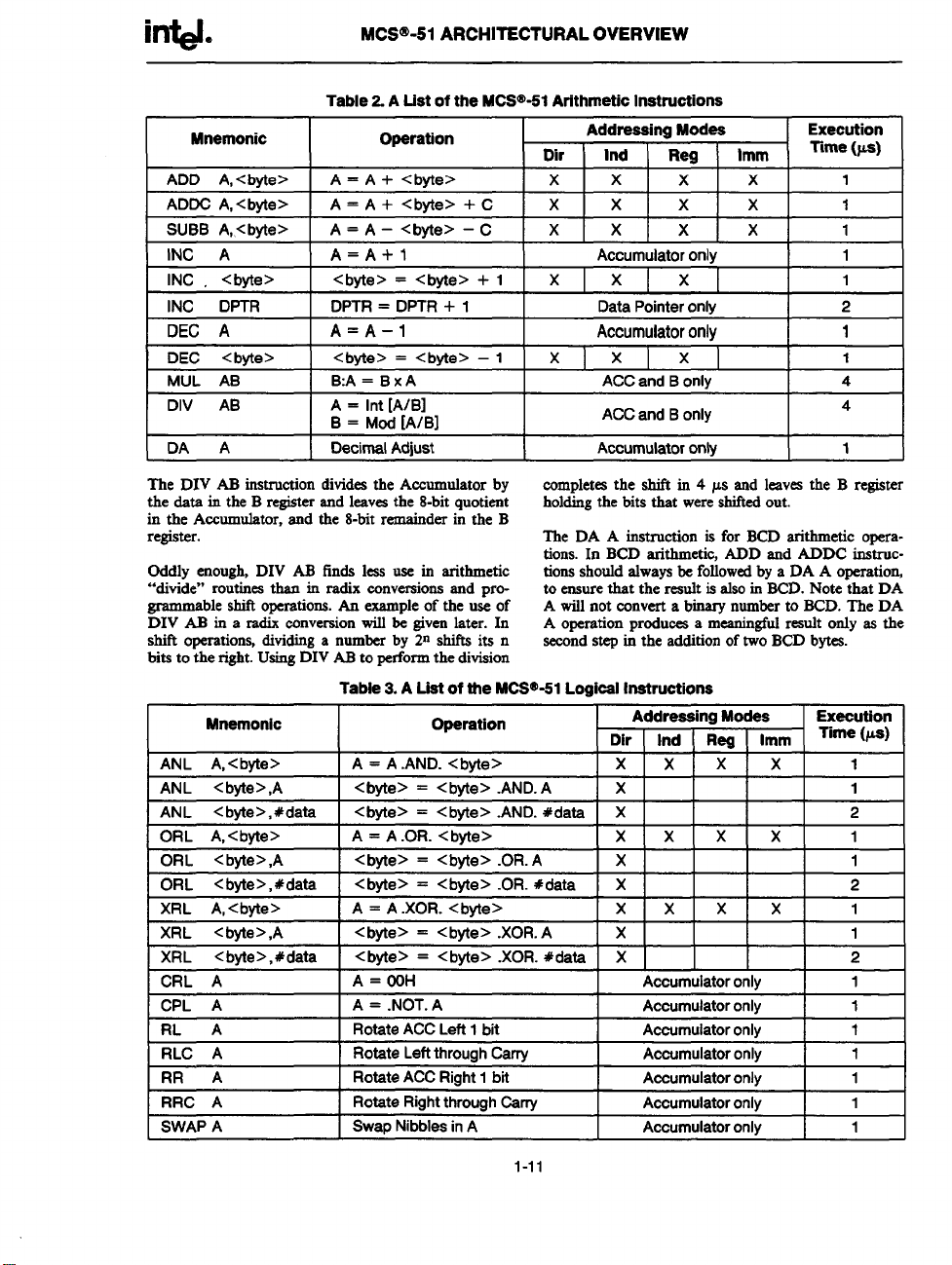
Arithmetic Instructions ...............................1-10
Logical lnstrudions ....................................l.l2
Data Tran#ers ...........................................l.l2
Boolean Instructions
Jump Instructions ......................................1-16
CPU TIMING .............................................l-l7
Machine Cycles .........................................1-18
Interrupt Structure ......................................l.2O
ADDITIONAL REFERENCES ...................1 -22
.................................................
..................................1-14
1-6
1-1
Page 8

Page 9
ir&L
INTRODUCTION
The
8051 is the original member of the MCW-51 family, and is the core for allMCS-51 devices. The features of the
8051 core are -
●
8-bit CPU optimized for control applications
●
Extensive Boolean processing (Single-blt logic) capabtilties
●
64K Program Memory address space
●
64K Data Memory address space
●
4K bytes of on-chip Program Memory
●
128 bytesof on-chip Data RAM
●
32 bidirectional and individually addressable 1/0 lines
●
Two 16-bit timer/counters
●
Full duplex UART
●
6-source/5-vector interrupt structure with two priority levels
●
On-chip clock oscillator
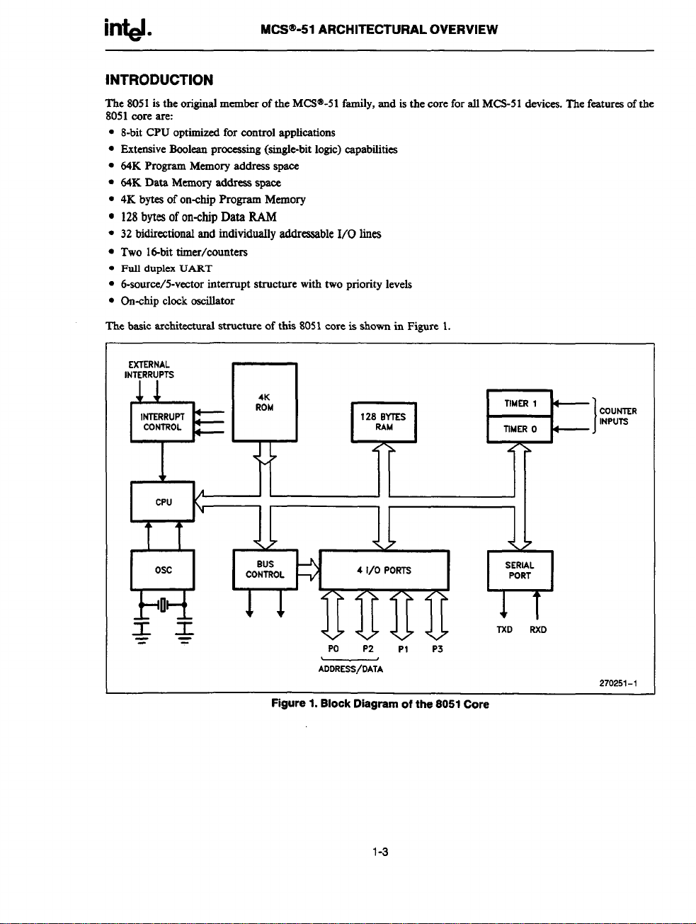
The basic architectural structure of this 8051 core is shown in Figure L
EXTERNAL
INTERRUPTS
,,
M~@.51 ARCHITECTURAL OVERVIEW
I
I
COUNTER
INPUTS
w II
BUS
CONTROL
11
H
4 1/0 PORTS
Po P2 PI P3
AODRESS/DATA
Figure 1. Block Diagram of the 8051 Core
1-3
H
SERIAL
PORT
Q
TXO RXD
270251-1
Page 10
intd.
MCS@-51 ARCHITECTURAL OVERVIEW
1-4
Page 11
i~.
MCS@’-5l ARCHITECTURAL OVERVIEW
1-5
Page 12
i~.
M~@.51 ARCHITECTURAL OVERVIEW
PROORAMMrhtosv
* ----------- --------------
8
1
1
1
1
1
1
1
I
1
I
o
8
0
0
0
8
0
0
9
I
I
I
,
1
I
:
#
o
0
1
0
@
*
I
:
●-
--- -------- -------- -.!
(REM ONLY)
FFFFw
T -
EXTERNAL
G=o m.1
2STERNAL
0000
IN7ERNAL :
Figure 2. MCW’-51 Memory Structure
CHMOS Devices
Functionally, the CHMOS devices (designated with
“C” in the middle of the device name) me all
compatible with the 8051, but being CMOS, draw less
current than an HMOS counterpart. To further exploit
the power savings available in CMOS circuitry, two re-
duced power modes are added
● Software-invoked Idle Mode, during which the CPU
is turned off while the RAM and other on-chip
peripherals continue operating. In this mode, current draw is reduced to
about 15% of the current
drawn when the device is fully active.
● Software-invoked Power Down Mode, during which
all on-chip activities are suspended. The on-chip
RAM continues to hold its data. In this mode the
device typically draws less than 10 pA.
Although the 80C51BH is functionally compatible with
its HMOS counterpart, s~lc differeneea between the
two types of devices must be considered in the design of
an application circuit if one
wiaheato ensure complete
interchangeability between the HMOS and CHMOS
devices. These considerations are discussed in the Ap
plieation
Note AP-252, “Designing with the
80C5lBH.
fiuy
OATAMEMORY
------------------------ . . . . .
t
$
s
8
I
I
1
1
1
I
8
1
1
I
I
1
1
I
1
1
:
1
o
1
#
8
1
9
1
8
1
1
8
1
0
I
0
1
9
1
t
1
#
I
I
,
,
1
B
I
: FfH: ------
I
0:
9,
:
e,
9
0
0
9
9
8
*
I
1
I
I 00
,1+
I
1
●-------- --------- ..- -. -.-:
(RW/WRlT2)
IN7ERNM
EXIERNALm
0000
8
8
I
I
0
I
*
0
I
I
#
I
I
I
I
-
I
I
1
:
1
I
I
I
1
I
1
1
0
1
J:
1
1% tiR
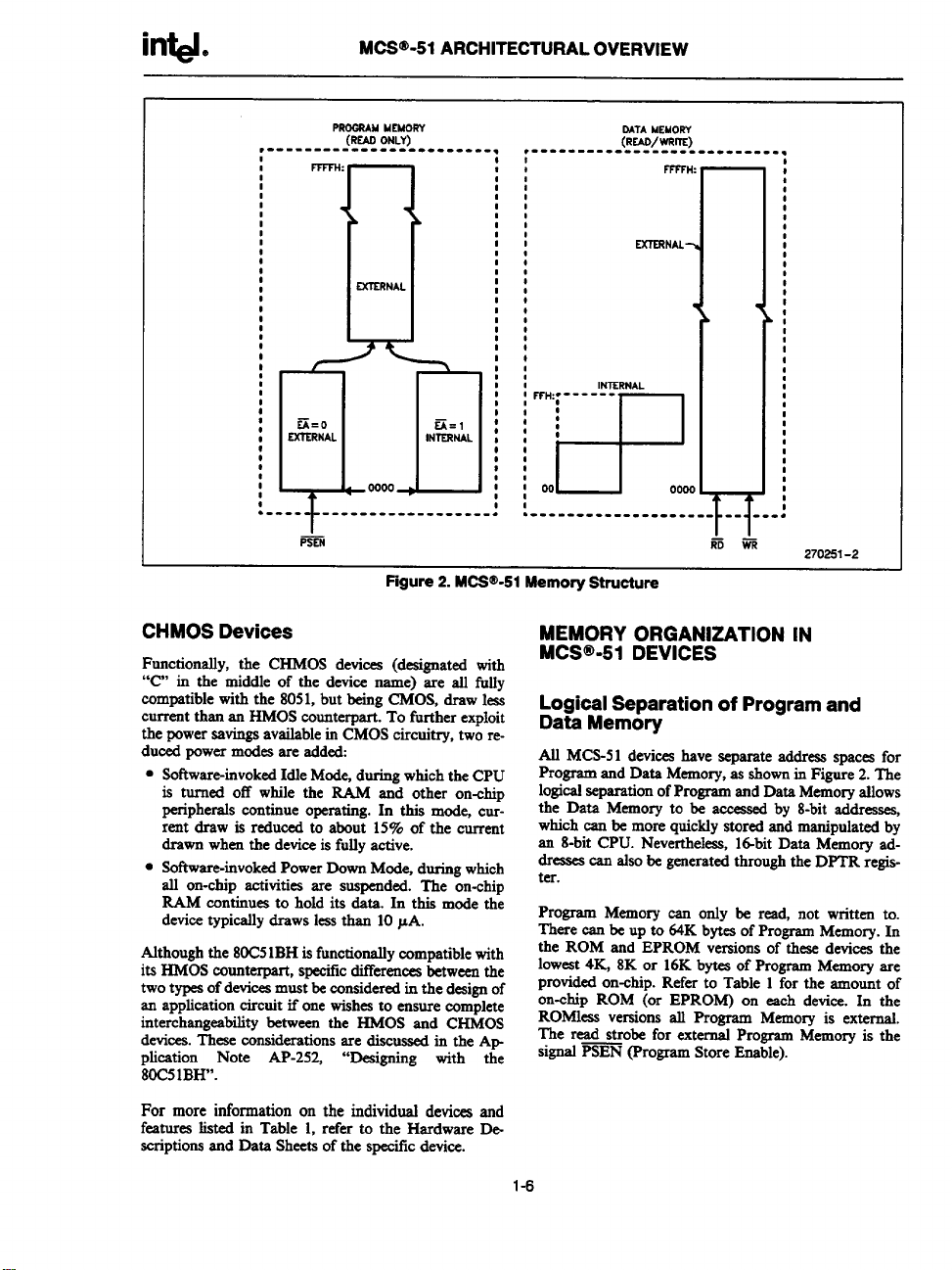
MEMORY ORGANIZATION IN MCS@-51 DEVICES
Logical Separation of Program and
Data Memory
AU MCS-51 devices have separate address spacea for
Program and Data Memory, as shown in Figure 2. The
logical separation of Program and Data Memory allows
the Data Memory to be acceased by 8-bit addressea,
which can be more quickly stored and manipulated by
an 8-bit CPU. Nevertheless, ld-bh Data Memory addresses can also be generated through the DPTR register.
Program Memory can only be read, not written to.
There can be up to 64K bytes of Program Memory. In
the ROM and EPROM versions of these devices the
loweat 4K, 8K or 16K bytes of Program Memory are
provided on-chip. Refer to Table 1 for the amount of
on-chip ROM (or EPROM) on each device. In the
ROMleas versions all Program Memory is external.
The read strobe for external Program Memory is the
signal PSEN @rogram Store Enable).
270251-2
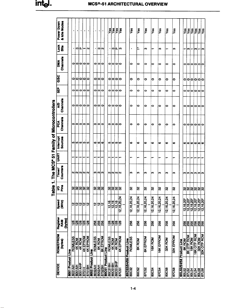
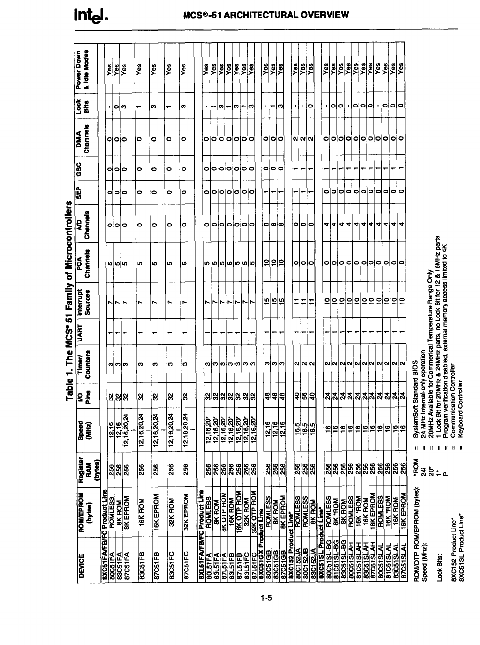
For more information on the individual devices and
features listed in Table 1, refer to the Hardware De
scriptions and Data Sheets of the specific device.
1-6
Page 13
intel.
MCS@-51 ARCHITECTURAL OVERVIEW
Data Memory occupies a separate addrexs space from
%OgrCt122 hkznory. Up to 64K bytes of exterttd RAM
can be addreased in the externrd Data Memo~.
The CPU generatea read and write signals RD and
~, as needed during external Data Memory accesses.
External Program Memory and external Data Memory
~~ combined if-desired by applying the ~ ~d
PSEN signals to the inputs of an AND gate and using
the output of the gate as the read strobe to the external
Program/Data memory.
ProgramMemory
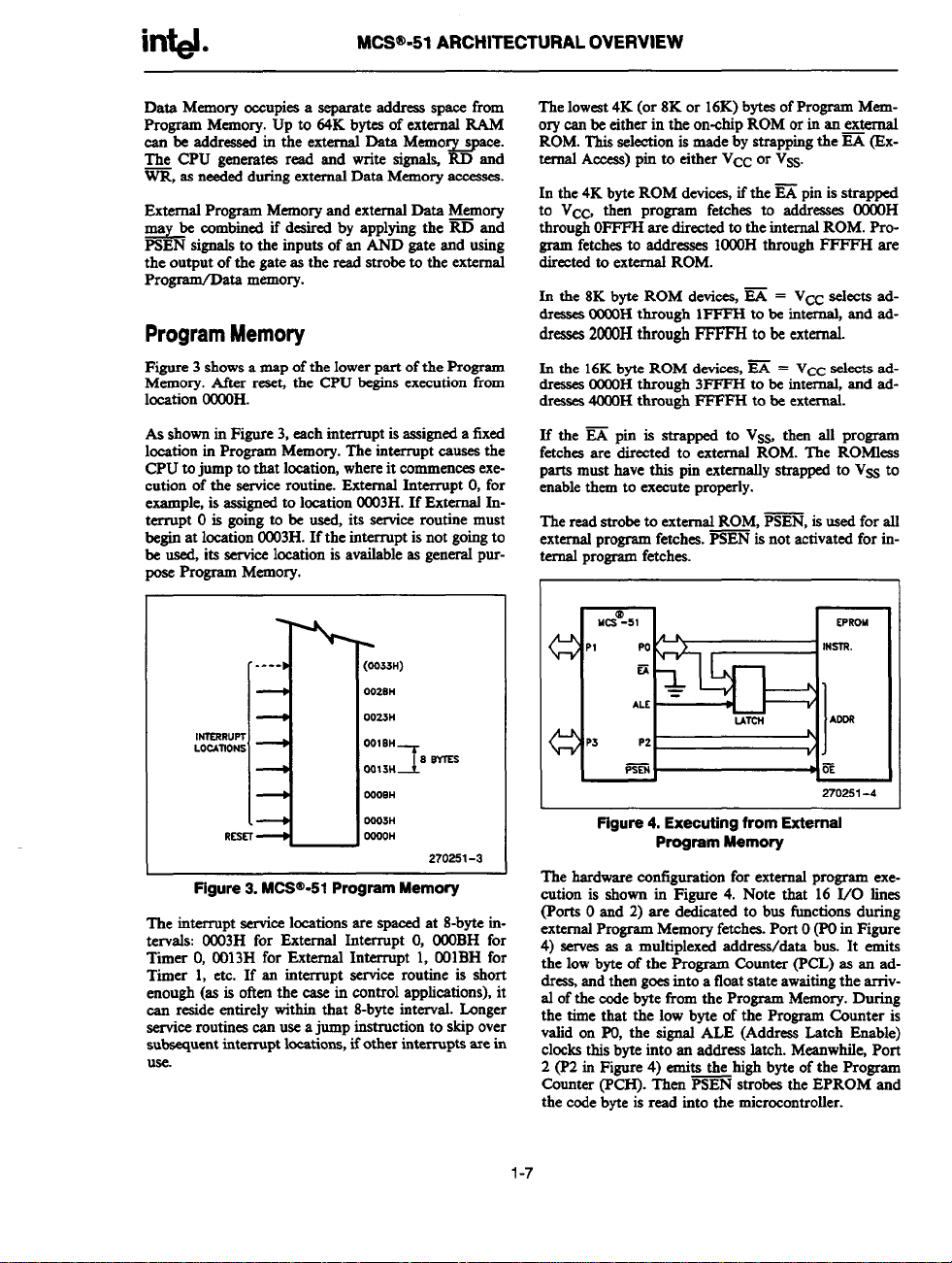
Figure 3 shows a map of the lower part of the Program
Memory. After reset, the CPU begins execution from
location OWOH.
AS shown in F@ure 3, each interrupt is
location in Program Memory. The interrupt causes the
CPU to jump to that location, where it commences execution of the serviee routine. External Interrupt O,for
example, is assigned to location 0003H. If External Interrupt O is going to & used, its service routine must
begin at location 0003H. If the interrupt is not going to
be used, its service location is available as general purpose Program Memory.
..-.
INTSRRUPT
LOCATIONS
R2S~
i
Figure 3. MCW’-51 Program Memory
The interrupt aeMce locations are spaced at 8-byte intervak 0U03H for External Interrupt O, 000BH for
Tmer O, 0013H for External Interrupt 1, 00IBH for
Timer 1, etc. If an interrupt service routine is short
enough (as is often the case in control applications), it
can reside entirely within
service routinea can use a jump instruction to skip over
subsequent interrupt locations, if other interrupts are in
use.
that 8-byte interval. Longer
assigned a tixed
&
(O033H)
002EH
002SH
00IBH
0013H
II
000SH
0003H
0000H
Ssvrm
270251-3
The lowest 4K (or SK or 16K) bytes of Program Memory can be either in the on-chip ROM or in an external
ROM. This selection is made by strapping the ~ (External Access) pin to either VCC or Vss.
In the 4K byte ROM devices, if the= pin is strapped
to VcC, then program fetches to addresses 0000H
through OFFFH are directed to the internal ROM. Program fetches to addresses 1000H through FFFFH are
directed to external ROM.
In the SK byte ROM devices, = = Vcc selects addresses (XtOOHthrough lFFFH to be internal, and ad-
dresses 2000H through F’FFFH to be external.
In the 16K byte ROM devices, = = VCC selects ad-
dresses 0000H through 3FFFH to be internal, and addresses 4000H through FFFFH to be external.
If the ~ pin is strapped to Vss, then all program
fetches are directed to external ROM. The ROMleas
parts must have this pin externally strapped to VSS to
enable them to execute properly.
The read strobe to externally: PSEN, is used for all
external oro.cram fetches. PSEN LSnot activated for in-
m%
‘s
m
=
ALE
l==
LArcn
Po
1
a’s ‘z~
Figure 4. Executing from External
Program Memory
The hardware configuration for external program execution is shown in Figure 4. Note that 16 I/O lines
(Ports O and 2) are dedicated to bus fictions during
external Program Memory f~hes. Port O(PO in Figure
4) servex as a multiplexed address/data bus. It emits
the low byte of the Program Counter (PCL) as an address, snd then goes into a float state awaiting the arrival of the code byte from the Program Memory. During
the time that the low byte of the Program Counter is
valid on PO, the signal ALE (Address Latch Enable)
clocks this byte into an address latch. Meanwhile, Port
2 (P2 in Figure 4) emits the high byte of the Program
Countex (WI-I). Then ~ strobex the EPROM and
the code byte is read into the microcontroller.
EPROM
INSTR.
AOOR
1
270251-4
1-7
Page 14
MCS@-51 ARCHITECTURAL OVERVIEW
Program Memory addresses are always 16 bits wide,
even though the aotual amount of Program Memory
used ntSy be kSS than 64K bytes. External prOq
exeoutiorssacrifices two of the 8-bit ports, PO and P2, to
the fisnction of addressing the Program Memory.
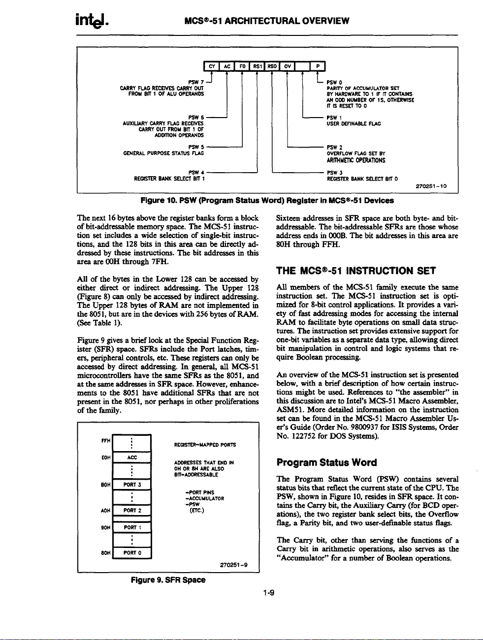
Data Memory
Theright
nal Dats Memory spaces available to the MCS-51 user.
F@ure 5 shows a hardware configuration for accessing
up to 2K bytes of external RAM. The CPU in this ease
is executing from internal ROM. Port O serves as a
multiplexed address/data bus to the RAM, and 3 lines
of Port 2 are bein~d to page the RAM. The CPU
generates = and WR signals as needed during exter-
ial WM
There ean be up to 64K bytea of external Data Memo-
ry. External Data Memory addresses can be either 1 or
2 bytes wide. One-byte addresses are often used in cxm-
junction with one or more other 1/0 lines to page the
R4M, as shown in Figure 5. Two-byte addresws ears
atso be used, irz which case the high address byte is
emitted
half of Figure 2 shows the internal and exter-
ameases. -
1’
Figure 5. Accessing External Data Memory.
If the Program Memory is Internal, the Other
Bits of P2 are Available as 1/0.
at Port 2.
I
270251-5
I
Internal Data Memory is mapped in Figure 6. The
memory space is shown divided into three bloeka,
which are generally referred to as the Lower 128, the
Upper 128, and SFR space.
Internal Data Memory addresses are always one byte
Wid%which implies an address space of only 256 bytes.
However, the addressing modes for intemssl RAM ean
in fact seeommodate 384 bytes, using a simple trick.
Direct addresses higher than 7FH awes one memory
space, and indirect addresses higher than 7FH access a
different memory space. Thus Figure 6 shows the Up-
per 128and SFR
addrq
cally separateentities;
BANK
SELECT
BRS IN
‘1 20H
Figure 7. The Lower 128 Bytes of internal RAM
The
Imwer 128 bytes of W are present in all
MCS-51 devices as mapped in F@ure 7. The lowest 32
bytes are grouped into 4 banks of 8 registers. Program
instructions call out these registers as RO through R7.
Two bits in the Program Status Word (PSW) seleet
which register bank is in use. This allows more effieient
use of code space, since register instructions are shorter
than instructions that use direet addreasiig.
spaceoccupyingthe ssme blockof
80H throu~ FFH, slthoud they are physi-
7FH
n
2FH
SN-ACORESSASLSSPACE
(S~ A~ESSES O-7F)
1
“{ lSH
‘0{ 10H
0’{ OBH
eo{o
1FH
17H
OFH
07H RESETVALUEOF
Ill
FFH
4 SANKSOF
8 REGIS7SRS
RO-R7
S7ACKPOIN7ER
270251-7
~:.. .-... -
, AC=IELE ACCESSIBLE
UPP~ , SV INDIREC7 BV OIRECT
: AtORESSING AODRSSSING
ONLY
SDH9 80H
‘m ACCESSIBLE
LOWER
SY 01REC7
128
ANOINC+REC7
o AGGRESSING
EP
Figure 6. Internal Data Memory
SPWAL
NC710N &oAmm~o
W
‘E~m CONTROLems
FFH
1
TIMER
RE—
STACKiolN7ER
ACCUMULATOR
(’nC.)
270251-6
NO SIT-AOORSSSABLE
SPACES
AVAIUBLE AS S7ACK
SPACEIN DEVICESWMI
256 BWES RAM
NOTIMPLE14EN7EDIN 8051
80H
I
Figure 6. The Upper 128 Bytes of Internal RAM
I-6
270251-8
Page 15
in~.
M~@-51 ARCHITECTURAL OVERVIEW
CTIAC]
CARRYFLAGRECEIVESCMi/fmw;
FROU BIT 1 Of ALU OPERANOS
AUXILIARYCARRYFLAGRECEIVES
CARRYOUT FROM B17 1 OF
AOOMON OPERANOS
GENERALPURPOSES7ATUSFLAG
REGtS7ERBANKSW’% t
-. .- . . . . . .- . . . . . . .. . . . ------ ----
Figure 1u. Psw (Progrsm ssssus worn) Register m mc5w-51 t2evtces
1
Psw6—
nw5
FOIRSIIRBO[ OVI
b a a
The next 16bytea above the register bankBform a block
of bit-addressable memory apace. The MCS-51 instruction set includes a wide seleetion of single-blt instructions, and the 128 bits in this area can be directly addressed by these irsstmctions. The bit addreascs in this
area are W)H through 7FH.
All of the bytes in the LQwer 128 can be accessed by
either direct or indirect addressing. The Upper 128
(Figure 8) can only be accessed by indirect addressing.
The Upper 128 bytes of RAM are not implemented in
the 8051, but me in the devices with 256bytea of RAM.
(Se Table 1).
Figure 9 gives a brief look at the Special Funotion Register (SFR) space. SFRS include the Port latchea, timers, pe2iphA controls, etc. l%ese registers can only&
-seal by dmect addressing. In general, all MCS-51
microcontrollers have the same SFRB as the 8051, and
at the same addresses in SFR space. However, enhancements to the 8051 have additional SFRB that are not
present in the 8051, nor perhaps in other proliferations
of the family.
“u
EOH
80H
AOH
90H
m
PORT.3
Porn 2
POR7 1
B
RE~MAPPSO POR7S
AOORESSES7NATENDIN
OH OR EN ARCALSO
B~-AOORESSABLE
-POR7 PINS
-ACCUMULATOR
-Psw
(E7c.)
J-A--I
270251-9
Figure 9. SFR Spsce
P
I
A
*
I
A
KWO
PARllYOFACCLWUIATORSS7
~ NARoWARCTO 1 IF IT CONTAINS
AN 000 NUMBEROF 1S, OTHERWISE
171SRESE7TO0
— Psw 1
USEROEFINABLEFUG
Psw 2
OVERFLOWFIAO SET BY
ARITIMCWOPERAl!ONS
Psw3
REOSJERBANKSELECTBll O
270251-10
!%teers addresses in SFR mace are both byte. and bit.
addressable. The blt-addre&able SFRS are ‘those whose
address ends in 000B. The bit addresses in this ares are
throUgh FFH.
80H
THE MCS@-51 INSTRUCTION SET
All
members of the MCS-51 family execute the same
instruction set. The MCS-51 instruction set is optimized for 8-bit control applications. It provides a variety of fast addressing modes for accessing the internal
MM to facilitate byte operations on small data structures. The instruction sd provides extensive support for
one-bit variables as a separate data t% allowing direct
blt manipulation in control and logic systems that require Boolean prmessirsg.
An overview of the MCS-51 instruction set is prrsented
below, with a brief description of how certain instructions might be used. References to “the assembler” in
this discussion are to Intel’sMCS-51 Macro Assembler,
ASM51. More detailed information on the instruction
set can be found in the MCS-51 Macro Assembler User’s Guide (Grder No. 9W3937 for 1S1SSystems, Grder
No. 122752 for DOS Systems).
Program Status Word
The Program Status Word (PSW) contains several
status bits that reflect the current state of the CPU. The
PSW, shown in Figure 10, resides in SFR space. It contains the Csrry bi~ the Auxdiary Carry (for BCD operations), the two register bank select bits, the Gvesflow
flag, a Parity bit, and two userdefinable status tlags.
The Carry bit, other than serving the functions of a
Carry bit in arithmetic operations, also sesws as the
“Accumulator” for a number of Boolean operations.
1-9
Page 16
MCS@-51 ARCHITECTURAL OVERVIEW
The bits RSOand RSl are wed to select one of the four
register banks shown in Figure 7. A number of instructions refer to these RAM locations as RO through R7.
The selection of which of the four banks is being referred to is made on the basis of the bits RSO and RS1
at execution time.
The Parity bit reflects the number of 1s in the Accumulator P = 1if the Accumulator contains an odd number of 1s, and P = O if the Accumulator contains an
even number of 1s.Thus
thenumber of 1s in the Accu-
mulator plus P is always even.
Two bits in the PSW are uncommitted and maybe used
as general purpose status flags.
Addressing Modes
The
addressing modes in the MCS-51 instruction set
are as follows
DIRECT ADDRESSING
In direct addressing the operand is specitied by an 8-bit
addreas field in the instruction. Only internal Data
RAM and SFRS can be directly addressed.
INDIRECT ADDRESSING
In indirect addressing the instruction specifies a register
which contains the address of the operand. Both internal and external RAM can be indirectly addressed.
The address register for 8-bit addresses can be RO or
RI of the selected register bank, or the Stack Pointer.
The addreas register for id-bit addresses can only be the
id-bit “data pointer” register, DPTR.
REGISTER INSTRUCTIONS
The
register banks, containing registers ROthrough R7,
can be accemed by certain instructions which carry a
3-bit register specification within the opcode of the instruction. Instructions that access the registers this way
are code efficient, since this mode elirninatez an addreas
byte. When the instruction is executedj one of the eight
registers in the selected bank is amessed. One of four
banks is selected at execution time by the two bank
select bits in the PSW.
IMMEDIATE CONSTANTS
The value of
a constant can follow the opcode in Pro-
gram Memory. For example,
MOV A, # 100
loads the Accumulator with the decimal number 100.
The same number could be specified in hex digitz as
64H.
INDEXED ADDRESSING
only
Program Memory can be amessed with indexed
addressing, and it can only be read. This addressing
mode is intended for reading look-up tables in Program
Memory. A Id-bit base register (either DPTR or the
Program Counter) points to the base of the table, and
the Accumulator is setup with the table entry number.
The address of the table entry in Program Memory is
formed by adding the Accumulator data to the base
pointer.
Another type of indexed addreaaing is used in the “case
jump” instruction. In this case the destination address
of a jump instruction is computed as the sum of the
base pointer and the Accumulator &ta.
Arithmetic Instructions
The
menu of arithmetic instructions is listed in Table 2.
The table indicates the addressing modes that can be
used with each instruction to access the <byte> operand. For example, the ADD A, <byte> instruction can
be written as
ADD A,7FH
ADD A,@RO (indirect addressing)
ADD A,R7 (register addressing)
ADD A, # 127 (iediate constant)
The execution times listed in Table 2 assume a 12 MHz
clock frequency. All of the arithmetic instructions execute in 1 ps except the INC DPTR instruction, which
takes 2 W, snd the Multiply and Divide instructions,
which take 4 ps.
Note that any byte in the internal Data Memory space
can be incremented or decremented without going
through the Accumulator.
(directaddressing)
REGISTER-SPECIFIC INSTRUCTIONS
Some instructions are specific to a certain register. For
example, some instructions always operate on the Accumulator, or Data Pointer, etc., so no address byte is
needed to point to it. The opcode itself does
that.In-
structions that refer to the Accurrdator as A assemble
as accumulator-specific opcmdes.
One of the INC instructions operates on the Id-bit
Data Pointer. The Data Pointer is used to generate
16-bit addresses for external memory, w being able to
increment it in one 16-bit operation is a usefirl feature.
The MUL AB instruction multiplies the Accumulator
by the data in the B register and puts the Id-bit product
into the concatenated B and Accumulator registers.
1-1o
Page 17
inl#
Mnemonic Operation
ADD A,<byte> A = A + <byte>
I ADDOA, <byte> I A= A+< byte>+C I X I X I X I X ] 1 I
SUBB A, <byte> A= A–<byte>-C
INC A
I INC . <byte>
I lhJC DPTR I DPTR = DpTR + 1 I
I DEC A
DEC <byte>
MUL
AB B.A=Bx A ACC and B only 4
DIV AB
I
IDAA I Decimal Adjust
MCS@-51 ARCHITECTURAL OVERVIEW
Table 2 A Ust of the MCS@I-51 Arithmetic Instructions
Addressing Modes
Dk I Ind Rq lmm
x
x x
I A=A+l I Accumulator onlv I 1
<byte> =<byte>+l I X I X I X I
I
I A= A-l
<byte> = <byte> – 1
A = Int [A/B]
B = MOd[A/Bl
I
I
x
I
x
Data Pointer only
Accumulator only
x x
I
ACC and
Accumulatoronly
B only
x x
x
x 1
Execution
Time (@
11-1
121
Ill
I
I
Ill
1
1
4
I
The DIV AB instruction divides the Accumulator by
the data in the B register and leevea the 8-bit quotient
in the Accumulator, and the 8-bit remainder in the B
register.
Oddly enough, DIV AB finds lees use in arithmetic
“divide” routines than in radix eonversions and pro-
~ble shift operstioILs. k example of the use of
DIV AB in a radix conversion will be given later. In
s~ operations, dividing a number by 2n shifts its n
bits to the right. Using DIV AS to perform the division
Table 3. A Uet of the MCS@J-51Logical Instructions
I
IRL A I Rotate ACC Left 1 bit I
Mnemonic
I
ANL A,< byte> A = A .AND. <byte> x x x x
ANL <byte>,A
ANL <bvte>, #data
ORL A,< byte>
ORL <bvte>,A
ORL <byte>, #data
XRL A,< byte> A = A .XOR. <byte> X1X1X
XRL <byte>,A
XRL <byte>, #data
CRL A
CPL A
RLC A
RR A
RRC A
SWAP A
<byte> = <byte> .AND. A
<byte> = <byte>
A = A.OR. <byte>
I
<byte> = <byte> .OR. A
<byte> = <byte> .OR. #data
I
<byte> = <byte> .XOR. A
I
<byte> = <byte> .XOR. #data I X
A=OOH
A =
Rotate Left through Csrry
I
Rotate ACC Right
Rotate Right through Carry
Swap Nibbles in A
Operation
.NOT. A
1 bit
eompletcs the shift in 4 p.s and leaves the B register
holding the bits that were shifted out.
The DA A instruction is for BCD arithmetic opera-
tions. In BCD arithmetic, ADD and ADDC instructions should always be followed by a DA A operation,
to ensure that the
A will not convert a binary number to BCD. The DA
A operation produces a meaningfid
second step in the addition of two BCD bytes.
red is also in BCD. Note that DA
Addressing Modes
Dir
Ind I Reg I
x 1
.AND. #data
x 2
X1X1X1X
I
x 1
x
x
I
Accumulator only 1
Accumulator
Accumulator onlv
Accumulator only
I
Accumulator only 1
Accumulator only 1
Accumulator
only
onlv 1
result only as the
Imm
x
I
I
I
Ill
I
Execution
Time (ps)
1
1
2
1
1
2
1
1
I
1-11
Page 18
irrtel.
MCS@-51 ARCHITECTURAL OVERVIEW
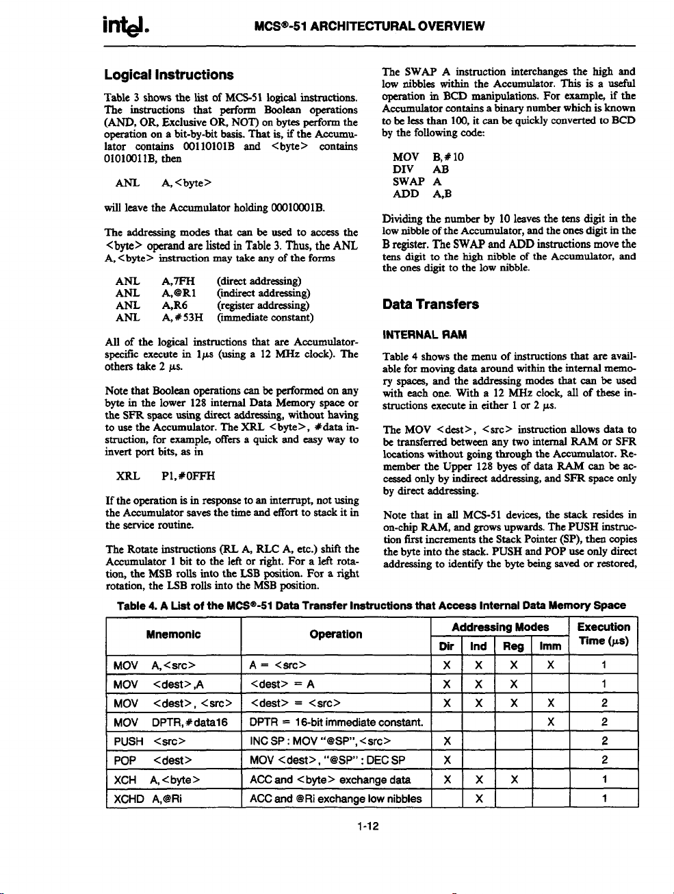
Logical Instructions
Table 3 shows the list ofMCS-51 logical instructions.
The instructions that perform Boolean operations
(AND, OIL Exclusive OIL NOT) on bytes perform the
operation on a bit-by-bit bssis. That is, if the AecumuIator contains 001101OIB and <byte> contains
O1OIOOIIB,then
ANL
will leave the Accumulator holding OOO1OOOIB.
The addrcasing modes that can be used to access the
<byte> operand are
A, <byte> instruction may take any of the forms
ANL A,7FH (direct addressing)
ANL A,@Rl
ANL
ANL
AU of the logical instructions that are Accumulatorspecflc execute in lps (using a 12 MHz clock). The
othem take 2 ps.
Note that Boolean operations can be performed on any
byte in the lower 128 internal Data Memory space or
the SFR space using direct addressing, without having
to use the Accumulator. The XRL <byte >, #data instruction, for example offets a quick and easy way to
invert port bits, as in
XRL Pl,#oFFH
If the operation is in response to an interrupt, not using
the Accumulator saves the time and effort to stack it in
the service routine.
The Rotate instructions (3U & RLC A, etc.) shift the
Aeeurtmlator 1 bit to the MI or right. For a left rota-
tion, the MSB rolls into the LSB position. For a right
rotation, the LSB rolls into the MSB position.
Table 4. A List of the MCS@-51 Data Tranafer Instructions that Access Internal Data Memory Space
MOV A, <src>
MOV <cleat> ,A
MOV <dest>, <src>
MOV DPTR,#data16
PUSH <WC>
POP
XCH A, <byte>
XCHD A,@Ri
A, <byte>
listedinTable 3. Thus, the ANL
A,R6 (register addressing)
A, # 53H (immediate constant)
Mnemonic Operation
<dest>
(indirect addressing)
A = <src>
<dest> = A
<dest> = <src>
DPTR = 16-bit immediate constant.
INCSP: MOV “@’SP’, <src>
MOV <dest>, “@SP”: DECSP x
ACCand <byte> exchange data
ACCand @Riexchange low nibbles
The SWAP A instruction interchanges the high and
low nibbles within the Accumulator. This is a useful
operation in BCD manipulations. For exampie+ if the
Accumulator contains a binary number which is known
to be leas thsn IQ it can be qnickly converted to BCD
by the following code:
MOV B,# 10
DIV AB
SWAP A
ADD A,B
Dividing the number by 10 leaves the tens digit in the
low nibble of the Accumulator, and the ones digit in the
B register. The SWAP and ADD instructions move the
tens digit to the high nibble of the Accumulator, and
the onea digit to the low nibble.
Data Transfers
INTERNAL RAM
Table 4 shows the menu of instructions that are available for moving data around within the internal memo-
ry spaces, and the addressing modes that can be used
with each one. Wkh a 12 MHz clock, all of these instructions execute in either 1or 2 ps.
The MOV < dest >, < src > instruction allows dats to
be transferred between any two internal RAM or SFR
lwations without going through the Accumulator. Remember the Upper 128 byes of data RAM can be acwased only by indirect addressing, and SFR space only
by direct addressing.
Note that in all MCS-51 devices, the stack resides in
on-chip RAM, and grows upwards. The PUSH instruc-
tion first increments the Stack Pointer (SP), then copies
the byte into the stack. PUSH and POP use only dkcct
addressing to identify the byte being
Addressing Modes
Ind Reg
Dir
saved or restored,
Execution
Time (ps)
Imm
x x x x
x x x
x x x x
x
x
x x x
x
1
1
2
2
2
2
1
1
1-12
Page 19
i~o
MCS@-51 ARCHITECTURAL OVERVIEW
but the stack itself is accessed by indirect addressing
using the SP register. This means the stack can go into
the Upper 128, if they are implemented, but not into
SFR space.
In devices that do not implement the Upper 128,if the
SP points to the Upper 128,PUSHed bytes are lost, and
POPped bytes are indeterminate.
The Data Transfer instructions include a id-bit MOV
that can be used to initialise the Data Pointer (DPTR)
for look-up tables in Program Memory, or for Id-bit
external Data Memory accesw.
The XCH A, <byte> instruction causes the Amu-
lator snd addressed byte to exchsnge data. The
A,@Ri instruction is similar, but only the low nibbles
are involved in the exchange.
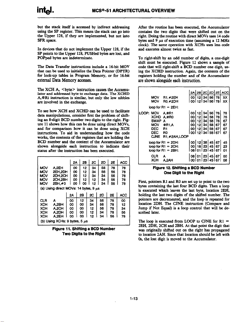
To see how XCH and XCHD can be used to fatitate
data manipulations, consider first the problem of shit%ing an 8digit BCD number two digits to the right. Figure 11 shows how this can be done using direct MOVS,
and for comparison how it can be done using XCH
instructions. To aid in understanding how the code
works, the contents of the registers that are holding the
BCD number and the content of the Accumulator are
shown alongside each instruction to indicate their
status after the instruction has been executed.
MOV A,2EH
MOV 2EH2DH % ;; : % ~
MOV 2CH:2BH 00 12
n3JMm
(a) Using direct MOVS 14 bytes, 9 ps
~
gm
(b) Using XCHS 9 bytes, 5 ps
Figure 11. Shifting a BCD Number
Two Dlgite to the Right
. .
XCHD
Atler the routine has been executed, the Accumulator
contains the two digits that were shitled out on the
right. Doing the routine with direct MOVSuses 14code
bytes and 9 ps of execution time (assuming a 12 MHs
clock). The same operation with XCHS uses less code
and executes almost twice as fast.
To right-shift by an odd number of digits, a one-digit
shift must be executed. Figure 12 shows a sample of
code that will right-shii a BCD number one digi~ using the XCHD instruction. Again, the contents of the
registers holding the number and of the Accumulator
areshownalongsideeachinstruction.
First, pointers RI and ROare setup to point to the two
bytea containing the last four BCD digits. Then a loop
is executed which leaves the last byte, location 2EIL
holding the last two digits of the shifted number. The
pointers are decrernented, and the loop is repeated for
location 2DH. The CJNE instruction (Compare and
Jump if Not Equal) is a loop control that will be described later.
The loop is executed from LOOP to CJNE for R1 =
2EH, 2DH, 2CH and 2BH. At that point the digit that
was originally shii out on the right has propagated
to location 2AH. Siice that location should be left with
0s, the lost digit is moved to the Accumulator.
MOV Rl, #2EH
MOV RO,#2DH
loop for R1 = 2EH
.00P MOV A,@Rl 00 12 34 56 78 76
XCHD A,@RO
SWAP A
MOV @Rl,A
DEC RI
DEC RO
CJNE Rl,#2AH,LOOP
Imp for RI = 2DH
loop for R1 = 2CH:
ioop for RI = 2BH:
CLR A
XCH A,2AH
Figure 12. Shifting a SCD Number
One Digit to the Right
m
00 12 34 56 78 76
00 12 34 58 78 67
00 12 34 58 67 67
00 12 34 58 67 67
00 12 34 56 67 67
00 12 36 45 67 45
00 18 23 45 67 23
0s
01 22 45 67 01
06
01 23 45 67 00
00 01 23 45 67 06
1-13
Page 20
M~@.51 ARCHITECTURAL OVERVIEW
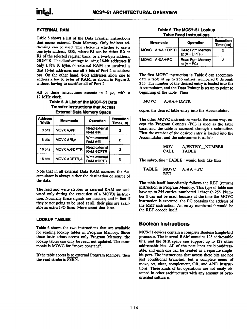
EXTERNAL RAM
Table 5 shows a list of the Data Transfer inatmctions
that acceas external Data Memory. Only indirect ad&easing can be used. The choice is whether to use a
one-byte address, @M where Ri can be either RO or
RI of the selected register bank, or a two-byte address,
@DPTR. The disadvantage to using 16-bit addresses if
only a few K
16-bit addresses use alf 8 bits of Port 2 as addreas
that
bytesof externalRAMare involvedis
bus. On the other hand, S-bit addresses allow one to
address a few K bytes of RAM, as shown in Figure 5,
without having to sacrifice all of Port 2.
Alf of these instructions execute in 2 pa, with a
12 MHz clock.
Tabfe 5. A
Trsnafer Instructions that Accees
Address
Width
8 b~
8 bb MOVX @Ri,A
‘6 bns ‘ovx “@DpTR
16 bfia
List of the MCS@-51 Data
Extarnsl Data Memory Spaoe
Mnemonic
MOVX A,@’Ri
‘ovx ‘DmR’A
Operation
Read external ~
RAM @Ri
Write external
RAM @Ri
Read external
RAM @DPTR
Writa exlemal
RAM @DPTR
Execution
Time (*)
2
2
2
Note that in all external Data RAM acaases, the Ac-
cumulator is always either the destination or source of
the data.
The read and write strobes to external RAM are activated only during the execution of a MOVX instruc-
tion. Normally these signals are inactive and in fact if
they’re not going to be used at u their pins are available as extra 1/0 lines. More about that later.
Table 6. Tha MCS3’-51 Lookup
Table Read Inetmctions
I
The first MOVC instruction in Table 6 can accommodate a table of up to 256 entries, numbered Othrough
255. The number of the desired entry is loaded into the
at (A + PC) -
Accumulator, and the Data Pointer is setup to point to
beginning of the table. Then
MOVC A,@A+DPTR
copies the desired table entry into the Accumulator.
The other MOVC instruction works the same way, except the Program Counter (PC) is used as the table
base, and the table is accewed through a subroutine.
First the number of the desired entry is loaded into the
Accumulator, and the subroutine is cslled:
MOV &ENTRY_NUMBER
CALL TABLE
The subroutine “TABLE” would look like this:
TABLE: MOVC A,@A + PC
The table itself immediately follows the RET (return)
instruction in Program Memory. This type of table can
have up to 255 entries, numbered 1through 255. Number O can not be used, because at the time the MOVC
instruction is executed, the PC contains the address of
the RET instruction. An entry numbered O would be
the RET opcode itseff.
1
LOOKUP TABLES
Table 6 shows the two instructions that are available
for reading lookup tables in Program Memory. Since
these instructions access only Program Memory, the
lookup tablea can only be read, not updated. The nmemonic is MOVC for “move constant”.
If the table access is to external Program Memory, then
the read strobe is PSEN.
Boolean Instructions
MCS-51 devices contain a complete Boolean (single-bit)
processor. The internal RAM contains 128 addressable
bits, and the SFR space can support up to 128 other
addressable blta. Afl of the port lines are bWaddressabl% and each one csn be treated as a separate singleblt port. The instructions that access these bits are not
just conditional branches, but a complete menu of
move, aeL clear, complement, OR and AND instmctions. These kinds of bit operations are not essily obtained in other architectures with any amount of byteOriented Sottware.
1-14
Page 21
intd.
MCS@-51 ARCHITECTURAL OVERVIEW
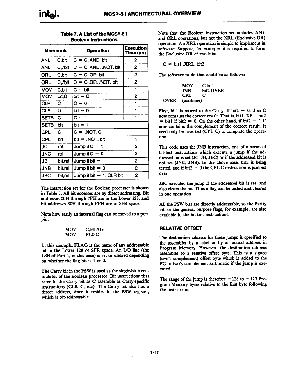
Table
7. A List of the MCS’@-51
Boolean Instrutilons
Mnemonic
ANL C,bit IC = C .AND. bit
ANL C./bit !C = C .AND. .NOT. bit I 2
nnl
n G.
Operation
I 1
16= C.OR. bit 2
Execution
Time (us)
2
I
MO\
MO\ UIL,U
F
ICLR c
CLR bit
SETB C
SETB bn Ibit= 1 1
CPL C IC = .NOT. C
CPL bit Ibit = .NOT. bit
JC
JNC rel Jump if C = O
JB bit,rel
JNB bit,rel Jump if bit = O
JBC bit,rel IJump if bti = 1; CLR bitI 2
The instruction set for the Boolean processor is shown
in Table 7. Alt bit ameaaca are by direct addressing. Blt
addreases OOHthrough 7PH are in the Lower 128, and
bit addresses 80H through FFH are in SFR space.
Note how easily an internal ilag can be moved to a port
pin:
In this example, FLAG is the name of any addressable
bit in the Lower 128 or SFR space. An 1/0 line (the
LSB of Port 1, in this case) is set or cleared depending
on whether the flag blt is 1 or O.
The bTy
mulator of the Boolean processor. Bit instructions that
refer to the Carry bit as C assemble as Carry-specflc
instructions (CLR C, etc). The Carry bit also has a
direct addreas, since it resides in the PSW register,
which is bit-addressable.
I UIL – w
Ic=o
]bit=o
Ic=l
rel
lJumpif C= 1
Jump if bti = 1
MOV C,PLAG
MOV
P1.o,c
1= I
1
1
1
I
1
1
2
2
2
2
bitinthePsW isused as the single-bitACCU.
Note that the Boolean instruction set includes ANL
and ORL operations, but not the XRL (_ExclusiveOR)
operation. An XRL operation is simple to implement in
sof?.ware.Suppose, for example, it is Wuired @ form
the Exclusive OR of two bits
C = bitl .XRL. bit2
The sot%vare to do that could be as follows:
MOV
OVER (continue)
1
Fkst, bit1 is moved to the Carry. If bit2 = O, then C
now contains the correct reauh. That is, bit 1 .XRL. bit2
= bitl ifbiti = O.On the other hand, ifbit2 = 1 C
now contains the complement of the correct result. It
need only be inverted (CPL C) to complete the opcrstion.
This code uses the JNB instruction, one of a series of
bk-teat instructions which execute a jump if the addressed bit is set (JC, JB, JBC) or if the addressed bit is
not set (JNG JNB). In the above case, blt2 is being
tested, and if bitZ = Othe CPL C instruction is jumped
over.
JBC executes the jump if the addressed bit is set, and
also clears the bit. Thus a fig can be teated and cleared
in one operation.
All the PSW bits are directly addressable so the Parity
bit, or the general purpose flags, for example, are also
available to the bit-test instructions.
RELATIVE OFFSET
The
the assembler by a label or by an actual address in
Program Memory. However, the destination address
assembles to a relative offset byte. This is a signed
(two’s complement) oftket byte which is added to the
PC in two’s complement arithmetic if the jump is exe-
cuted.
The range of the jump is therefore -128 to + 127Pro-
gram Memory bytes relative to the first byte following
the instruction.
CPL C
destination address for these jumps is specitied to
C,bit 1
bit2,0VER
1-15
Page 22
i~.
MCS@-51 ARCHITECTURAL OVERVIEW
Jump lnstruMlons
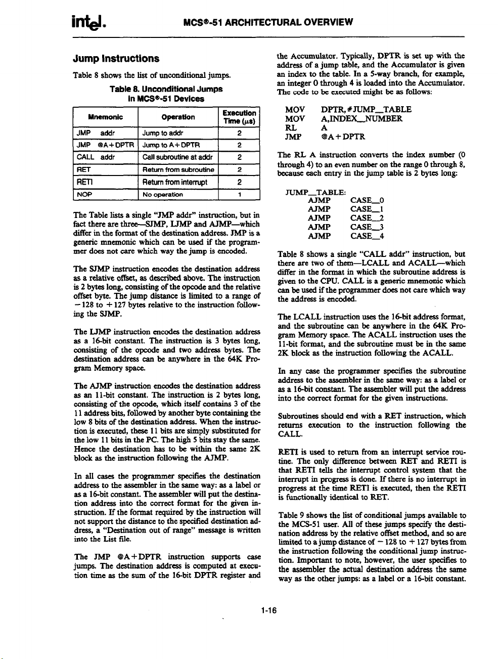
Table 8 shows the list of unconditional jumps.
Table 8. Unconditional Jumps
in MCW’-51 Oavices
Mnarnonic
I
I JMP addr
JMP @A+ DPTR I Jump to A+ DPTR
CALL addr I Call subroutine at addr
1RET
IRETI
NOP
The Table lists a single “JMP addr” instruction, but in
fact there are three-SJMP, LJMP and AMP-which
differ in the format of the destination address. JMP is a
generic mnemonic which can be used if the programmer does not care which way the jump is eneoded.
The SJMP instruction eneodes the destination address
as a relative offset, as deaeribed above. The instruction
is 2 bytes long, eonsiating of the opeode and the relative
offset byte. The jump distance is limited to a range of
-128 to + 127bytes reIative to the instruction follow-
ing the SJMP.
The LJMP instruction eneodea the destination address
as a Id-bit constant. The instruction is 3 bytes long,
consisting of the opeode and two address bytes. The
destination address ean be anywhere in the 64K Program Memory
The AJMP instruction encodesthe destination address
asan 1l-bit constant. The instruction is 2 bytee long,
eonaisting of the opode, which itself contains 3 of the
11address bits, followed by another byte containing the
low 8 bits of the destination address. When the instruction is executed, these 11bits are simply substituted for
the low 11 bits in the PC. The high 5 bits stay the same.
Hence the destination has to be within the same 2K
block as the instruction following the AJMP.
In all eases the programmer specifies the de&nation
address to the assembler in the same way as a label or
as a id-bit constant. The assembler will put the destination address into the eormct format for the given instruction. If the format required by the instruction will
not support the distance to the specified destination rtddresa, a “Destination out of range”
into the Lkt fde.
The JMP @A+ DPTR instruction supports ease
jumps. The destination address is computed at exeeu-
tion time as the sum of the lti-bit DPTR register and
SPSW.
Operation
I
I Jumo to addr
I Returnfromsubroutine I z I
Returnfrominterrupt I 2 I
I
No oparation
Exeeution
Tilna (us)
121
2
I
2
1
message is written
the Accumulator. Typically, DPTR is set up with the
addms of a jump table, and the Accumulator is given
an index to the table. In a 5-way branch, for examplq
an integer Othrough 4 is loaded into the Accumulator.
The code to be executed might be ax follows
MOV
MOV
RLA
JMP
The RL A instruction converts the index
through 4) to an even number on the range Othrough 8,
because each entry in the jump table is 2 bytee long:
~P_TABLE
Table 8 shows a single “CALL addr” instruction, but
there are two of them-LCALL and ACALL-which
differ in the format in which the subroutine address is
given to the CPU. CALL is a generic mnemonic which
ean be used if the programmer does not care which way
the address is encoded.
The LCALL instruction uses the Id-bit address format,
and the subroutine ean be anywhere in the 64K Program Memory space. The ACALL instruction uses the
1l-bit format, and the subroutine most be in the same
2K bkxk as the instruction following the ACALL.
In any case the programmer specifies the subroutine
address to the assembler in the same way as a label or
as a 16-bit constant. The assembler will put the address
into the correct format for the given instructions.
Subroutines should end with a RET instruction, which
returns execution to the instruction following the
CALL.
RETI is used to return from an interrupt service rou-
tine. The only difference between RET and RETI is
that RETI tells the interrupt control system that the
interrupt in progress is done. If there is no interrupt in
progress at the time RETI is executed, then the RETI
is functionally identical to RBT.
Table 9 shows the list of conditional jumps available to
the MCS-51 user. All of these jumps specify the desti-
nation address by the relative ot%et meth~ and so are
lindted to a jump distance of – 128to + 127 bytes from
the instruction following the conditional jump instruc-
tion. Important to note, however, the user speeifies to
the assembler the actual destination address the same
way as the other jump as a label or a id-bit constant.
DPTR, #JUMP_TABLE
A,INDEX_NUMBER
@A+DPTR
MMP
AJMP
AJMP
AJMP
CASE_O
CASE_l
CASE_2
CASE_3
CASE_4
number (O
1-16
Page 23

i~.
Mnemonic
JZ rei
JNZ rel
DJNZ <byte>
CJNE A, <byte> ,rei
CJNE <byte> ,#data,rei
,rel
MCS@-51 ARCHITECTURAL OVERVIEW
Table 9. Conditions Jumps in MCS@-51 Devioes
Operation
Jump if A = O
Jumpif A+O
Deorement and jump if not zero x
Jumpif A # <byte>
Jumpif <byte> # #data
Addressing Modes
ind
Dir
Accumulator oniy
Accumulator oniy
x
x x
Rag imm
x
x
Execution
Time (ps)
2
2
2
2
2
There is no Zero bit in the PSW. The JZ and JNZ
instructions test the Accumulator data for thst ccmdition.
The DJNZ instruction (Dezrement and Jump if Not
Zero) is for loop control. To execute a loop N times,
load a counter byte with N and tersnina
a DJNZ to the beginning of the loop, as shown below
for N = 10:
LOOP: (begin loop)
The CJNE instruction (Compare and Jump if Not
Equal) can also be used for loop control as in Figure 12.
Two bytes are specified in the operand field of the instruction. The jump is executed only if the two bytes
are not equal. In the example of Figure 12, the two
bytes were the data in R1 and the constant 2AH. The
initial data in R1 was 2EH. Every time the loop was
executed, R 1 was decresnertted,and the looping was to
continue until the R1 &ta reached 2AH.
Another application of this instruction is in “great=
than, less than” comparisons. The two bytes in the op
erand field are taken as unsigned integers. If the first is
less than the second, then the Carry bit is set (l). If the
first is greater than or equal to the second, then the
Carry bit is cleared.
CPU TIMING
All
which can be used if desired as the clock source for the
CPU. To use the on-chip oscillator, connect a crystal or
ceramic resonator between the XTAL1 and XTAL2
pins of the microcontroller, and capacitors to ground as
shown in Figure 13.
MOV
(;d Imp)
DJNZ
(continue)
MCS-51 microcontrollers have an on-chip oscillator
com~#lo
●
*
COUNTER,LOOP
te the loop with
1-17
@
Mes-51
HIAOS
ORCHMOS
57.
SmLS
STAL2
STAL1
Vss
nut
Vss
STAL7.
S-TAL1
Vss
=
w’%
HMOS
ORCnuos
Mcs”-51
HMOS
ONLY
Mm%!
CHMOS
ONLY
270251-11
270251-12
270251-13
270251-14
OUART&&~WA; > Cl
RrsONAmR
‘4-J
Figure 13. Using the On-Chip Oeciilator
CLOCK STAL1
SIGNAL
-4-I
EilSRNAL
WRNAL
Figure 14. Using an Externai Ciock
=
A. HMOS or CHMOS
CLOCK
-i-l
=
B. HMOS Only
(w) STU.2
L=
u
s
C. CHMOS only
Page 24
i~.
MCS’5’-51 ARCHITECTURAL OVERVIEW
Examples of how to drive the clock with an external
oscillator are shown in Figure 14. Note that in the
HMOS devices (S051, etc.) the signal at the XTAL2 pin
actually drives the internal clock generator. In the
CHMOS devices (SOC5lBH, ete.) the signsl at the
XTAL1 pin drives the internal clock generator. If only
one pin is going to be driven with the external oscillator
signal, make sure it is the right pin.
The internal clock generator defmea the sequence of
states that make up the MCS-51 machine cycle.
51 52 as se as .% s 52 as S4.SE as 51
Plm Prps PIP2 PIPS PIPs
(%L)
ALE
!
I
I - nw OPCODE.
READ NEXT
:,,-4ir-NEmo”oOEAGA~
(A)t-byts,l-eydshs2mdh,
I
I
I
e.g., WC A.
READ OPCODE.
r I
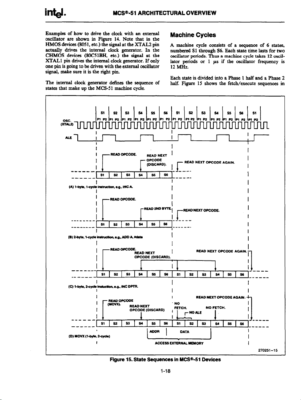
Machine Cycles
A machine cycle consists of a sequence of 6 statea,
numbered S1through S6. Each state time lasts for two
oscillator periods. Thus a machine cycle takes 12 Oscillator periods or 1 ps if the oscillator frequency is
12 MHz.
Each state is divided into a Phase 1 half and a Phase 2
half. Figure 15 shows the fetch/execute sequences in
Pips PIPS Pips PIP2
I
I
I
mm
L
P2 PIPS
Pips
I
1
I
J
I
I
I
(B)
2-byte. 1*
I
lm@s2b. *.e.. Aoo A,mdma
I
I
-------
-------
[c)
l-byle,2qs4C imhlesm ●.s., INC DPTR.
------
----- -
[0)
MOW (l-, S-c@@
S1 as es e4ae Seslases e4aEes
I
I
— READ OPCOOE
I
(MWX).
I
I
?
sla2a2s4] as eel S11S21S2]24SSSS
I
Figure 15. Stete Sequences in MCS@’-5l Devices
i
I
OPCOOE (DISCARD).
[
READ NEXT
OPCOOE (OISCARD) , ‘1=””
AOOR
I
I
I I
I
NO
1~
I
ACCESS EXTERNAL MEMORY
1-18
READ NEXT OPCODE AGAIN. ~
RSAO NEXT OPCODE AGAIN.
~NOALE
DATA
NO FETCH.
J
I
I
I
I
1
I
I
I
1
1
, j
-----
------
I
I
I
I
-----
.-----
I
270251-15
,,;
Page 25
in~e
MCS@-51 ARCHITECTURAL OVERVIEW
states and phases for various kinds of instructions. NormalIy two program fetches sre generated during each
machine cycle, even if the instruction being executed
doesn’t require it. If the instruction being executed
doesn’t need more code bytes, the CPU simply ignores
the extra fetch, and the Program Counter is not incremented.
Execution of a one-cycle instruction (Figure 15A and
B) beginsduring State 1of the machine cycle when the
opcode is latched into the Instruction Register. A second fetch occurs during S4 of the same machine cycle,
Execution is complete at the end of State 6 of this mschine cycle.
The MOVX instructions take two machine cycles to
execute. No program fetch is generated during the see
ond cycle of a MOVX instruction. This is the ordy time
program fetches are skipped. The fetch/execute sequence for MOVX instructions is shown in Figure
15(D).
ONE MACHINE CVCLS
ALE
-N ~
ro
P2
sl[a21s21s41aslss SIIS21S21S41SE 126
r
I
I
I
1
1
1
PCH OUTX
PCH OUT
1
I
t~::$m
T
I
1
I
L
PCH OUT
r
x’
I
I
I
1
[
x
t5i:F
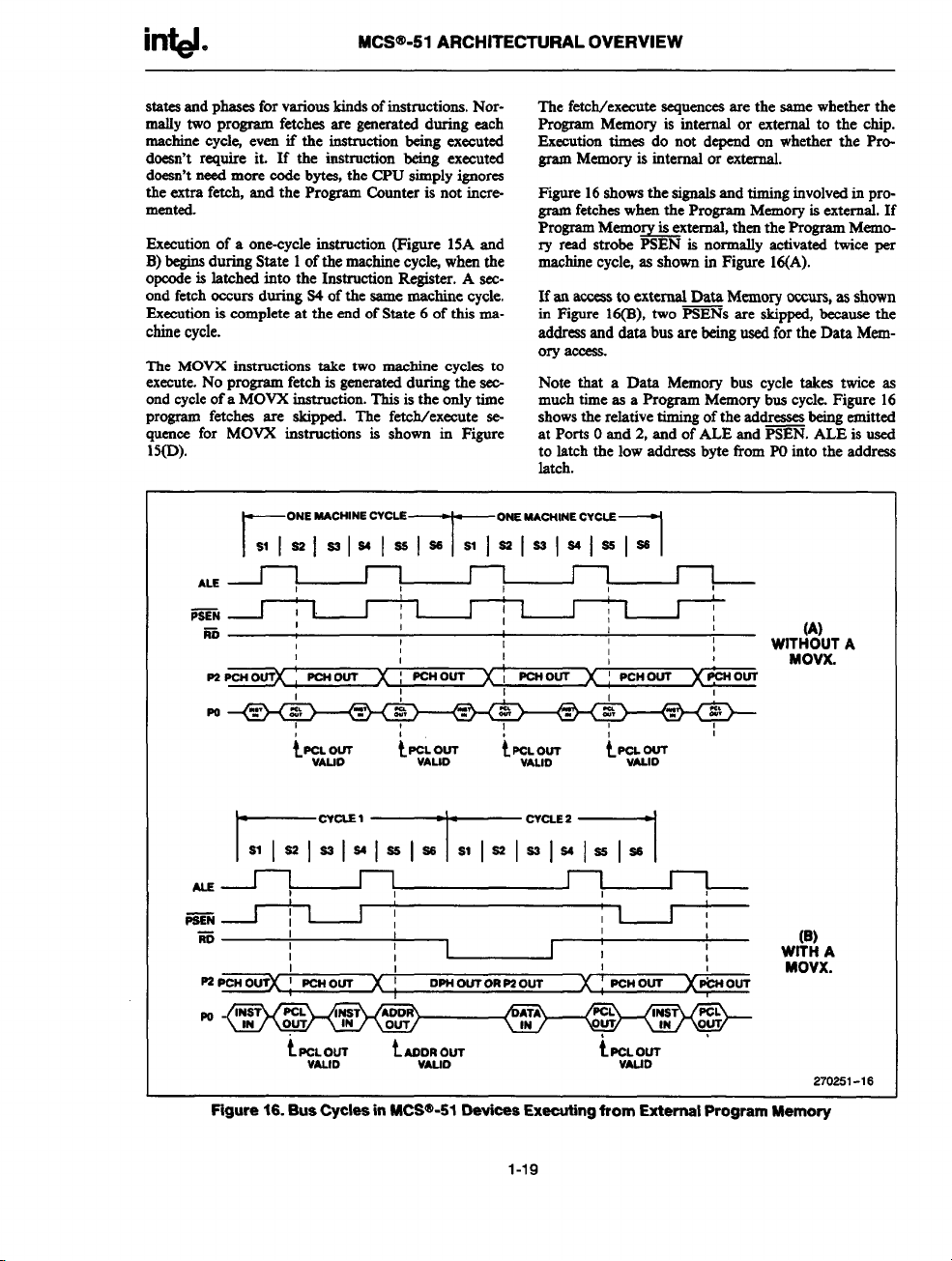
The fetch/execute sequences are the same whether the
Program Memory is internal or external to the chip.
Execution times do not depend on whether the Program Memory is internal or external.
Figure 16 shows the signals and timing involved in program fetches when the Program Memory is external. If
Program Memo~xternsl, then the Program Memory read strobe PSEN is normally activated twice per
machine cycle, as shown in Figure 16(A).
If an access to external Data Memory occurs, as shown
in Figure 16(B), two PSENS are skippe$ because the
address and data bus are being used for the Data Memory access.
Note that a Data Memory bus cycle takes twice as
much time as a Program Memory bus cycle. Figure 16
shows the relative timing of the addresses being emitted
at Ports Oand 2, and of ALE and PSEN. ALE is used
to latch the low address bvte from PO into the address
latch.
ONE MACIUNE CYCLE
1
I
I
1 I
I
I
PCNOUT
I
I
ty;LL&T &T
1
1
I I
1
I
1
1
I
!
,
1
I
I
1
I
I
1
WITH%)UT A
MOVX.
G:v:m’lxm:m
)
I
-N ~
E
P2PcHc@(
Figure 16. Bus Cycles in MCS@-51 Oevices Extilng irom External Program Memory
1 1
I
I
I
! PCHOUT
t P&m&T iAC:O&UT
I I
I
I
I
I
x!
OPH OUT OR P2 OUT
1-19
I
1 I
1
I
I
PCH OUT )( PWOUT
x:
,
1
1
I
I
I
1
(B)
WITH A
MOVX.
2702!31 -16
Page 26
i~e
MCS@-51 ARCHITECTURAL OVERVIEW
When the CPU is executing from intemrd Program
Memory, ~ is not activated, and program addresses are not emitted. However, ALE continues to be activated twice per machine cycle and so is available as a
clock output signal. Note, however, that one ALE is
skipprd during the execution of the MOVX instmction.
Interrupt Structure
The
8051 core provides 5 interrupt sources 2 external
interrupts, 2 timer interrupts, and the serial pat interrupt. What follows is an overview of the interrupt
structure for the t3051.Other MCS-51 devices have ad-
ditional interrupt sources and vectors as shown in Table 1. Refer to the appropriate chapters on other devices for further information on their interrupts.
INTERRUPT ENABLES
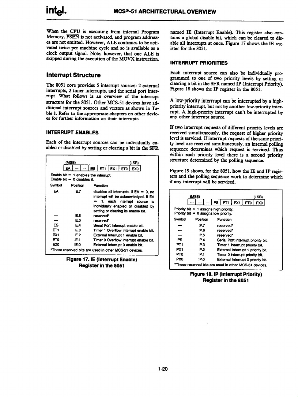
Each of the interrupt sources can be individually enabled or disabled by setting or clearing
(MSB)
EAl —
I—IESIETI IEXIIETOIEXO
Enablebk = 1 enablesb interqf.
Ensblebk =odieabksit
symbol Pmiti9n
EA
—
—
ES
ETl IE.3
Exl
ETo IE.1 TimerOflwrffw Interruptenabfebm
Exo
“Thesereservedbiteare usedinotherMCS-51devices.
IE.7
IE.6
IE.5
IE.4
IE.2
IE.O
Figure 17. IE (Interrupt Enable)
Function
d&bles all intempts. If EA = O,no
interruptW be acknowledged.If EA
= 1, each intenupt source is
itiiuslfy enabled or disebled by
settingw clearing iteeneblebit.
reserved”
reewed”
Ser!41Pwf Intemuptenabletin.
TImw 1 OverflowInterrupteneblebit
Gtsmsl Intenupf1 enablebit
EstemslIntenuptOenablebit
Register in the 8051
a bit in the SFR
(LSB)
natned IE (Interrupt Enable). This register also contains a global disable bit, which can be cleared to disable all interrupts at once. Figure 17 shows the IE register for the 8051.
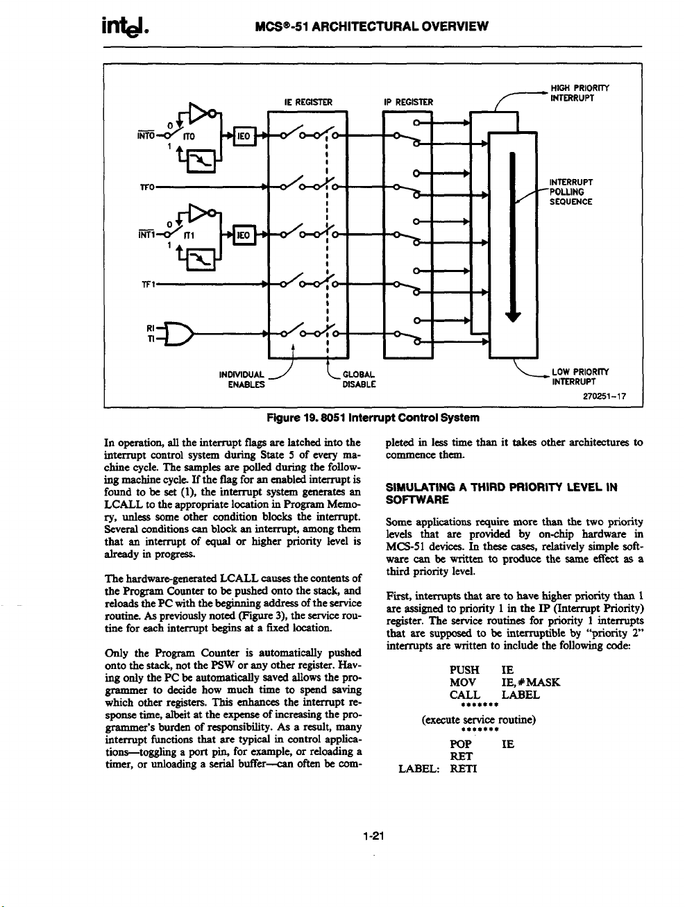
INTERRUPT PRIORITIES
Each interrupt source can also be individually pro~ed t? one of two
clearing a blt m the SFR named 1P (Interrupt Priority).
priority levels by setting or
Figure 18 shows the 1P register in the 8051.
A low-priority interrupt w be interrupted
bya high-
priority interrupt, but not by another low-priority interIUpt. A high-priority
interruptcan’tbeinterruptedby
any other interrupt source.
If two interrupt rquests of different priority levels are
received simultaneously, the request of Klgher priority
level is serviced. If interrupt requests of the same prioritylevel are received simultaneously, an interred polling
sequence determines which request is serviced. Thus
within each priority level there is a second priority
structure determined by the polling sequence.
Figure 19shows, for the 8051, how the IE and IP regieters and the polling sequence work to determine which
if any inttipt Wiilbe-serviced.
(MSB)
—
——
Prforifybit=lsssign shighpriwity.
Prioritytit = OassignslowprWity.
symbol
—
—
Ps IP.4
PTl IP.3 Timer1 intenuptpfbritybfi.
Pxl
PTo
Pxo fP.o
“Theseresewedtits are usedin otherMCB-51devices.
IPSIPTI IPXIIPTOIPXO
POeitiQn
IP.7
IP.6
IP.5 reserved-
IP2
lP.1
Functfon
resewed”
rewed”
SerialPorfinterruptp+eritybii
ExternalIntenupt1 ptirity bit.
limsr Ointerruptpriorftybii
ExternalIntellupto priorityMt.
Figure 18. 1P(Interrupt Priority)
Register in the 8051
(LSB)
1-20
Page 27
intd.
1 I
TFo
1
7FI J&o
RI
n
M~@-51 ARCHITEC~RAL OVERVIEW
IE REGISTER
+h-O+io
I
/&+.
1
-&-J.
J+
Figure 19.8051 Intermpt control system
I
:
I
I
:
I
A
.-
1PREGISTER
o
e b
o
0 b
0
b
●
➤
HIGHPRIORllY
INTERRUPT
1.
INTERRUPT
‘POLUNG
SEQUENCE
v
\
~ LyPwPNrr
270251-17
In operatiom all the interrupt tlags are latched into the
interrupt control system during State 5 of every machine cycle. The samples are polled during the following machine cycle-If the flag for an enabled interrupt is
found to be set (l), the interrupt system generates an
LCALL to the appropriate location in Program Memory, unless some other condition blocks the interrupt.
Several conditions can block an interrupt, among them
that an interrupt of equal or higher priority level is
already in progress.
The hardware-generated LCALL csusea the contents of
the Program Counter to be pushed onto the stack, and
reloads the PC with the beginning address of the service
routine. As previously noted (Rgare 3), the service routine for each interrupt begins at a fixed location.
Only the Program Counter is automatically pushed
onto the stack, not the PSW or any other register. Having only the PC be automatically saved allows the programmer to decide how much time to spend saving
which other registers. This enhances the interrupt response time, albdt at the expense of increasing the pro-
-er’s bu~en of responsibility. As a result, many
snterrupt functions that are typical in control applics-
tions-togghmg a port pim for example, or reloading a
timer, or unloading a serial but%r-can otten be mm-
pleted in lms
commence them.
SIMULATING A THIRD PRIORITV LEVEL IN
SOFIWARE
Some applications
time than it takes other architectures to
require more than the two priority
levels that are provided by on-chip hardware in
MCS-51 devices. In these cases, relatively simple software can be written to produce the same effect as a
thkd priority level.
Firat, interrupts that are to have higher priority than 1
are ssaigned to priority 1 in the 1P (Interrupt Priority)
register. The service routines for priority 1 interrupts
that are supposed to be interruptible by “priority 2“
interrupts are written to include the following code
PUSH IE
●******
●******
IE, #MASK
LABEL
MOV
CALL
(execute service routine)
POP IE
RET
LABEL RETI
1-21
Page 28
MCS@I-51 ARCHITECTURAL OVERVIEW
As soon as any priority 1 interrupt is acknowledged,
the IE (Interrupt Enable) register is m-defined so as to
disable all but “priority 2“ interrupts. Then, a CALL to
LAEEL exeoutes the RETI instruction, which clears
the priority 1 interrupt-in-program tlip-flop. At this
point SIly priority 1 interrupt that is enabled can be
seticed, but
Ody “priority’ 2“ illtCSTUptSare enabled.
POPping IE restores the original enable byte. Tberr a
normal RET (rather than another RETI) is used to
terminate the service routine. The additional software
adds 10 ps (at
12MHz) to priority 1interrupts.
ADDITIONAL REFERENCES
The following application notes are found in the Em-
bedded Chstml AppIicatwns
ber: 270648)
1. AP-69 “An Introduction
gle-Chip Microcomputer Family”
2. AP-70 “Using the Intel MCW-51 Boolean Processing Capabtities”
handbook. (Order Num-
to the Intel MCS@-5I Sin.
1-22
Page 29
MCS@51Programmer’s 2
Guide and Instruction Set
Page 30

Page 31

MCWI51 PROGRAMMER’S CONTENTS
GUIDE AND MEMORYORGANIZATION
INSTRUCTION SET PROGRAM MEMORY
DataMemory
INDIRECT ADDRESS AREA,...........,.........2-6
DIRECT AND INDIRECT ADDRESS
AREA ......................................................2-6
SPECIAL FUNCTION REGISTERS............2-8
WHAT DO THE SFRS CONTAIN JUST
AFTER POWER-ON OR A RESET,......,,2-9
...............................................2-4
PAGE
........................2-3
.................................2-3
SFR MEMORY MAP
PSW: PROGRAM STATUS WORD. BIT
ADDRESSABLE
PCON: POWER CONTROL REGISTER.
NOT BIT ADDRESSABLE .....,..,........,..2-11
INTERRUPTS
IE: INTERRUPT ENABLE REGISTER.
BIT ADDRESSABLE
ASSIGNING HIGHER PRIORITY TO
ONE OR MORE INTERRUPTS..,.........,2-13
PRIORITY WITHIN LEVEL
1P:INTERRUPT PRIORITY REGISTER.
BIT ADDRESSABLE ..,..........,.,,...........2-13
TCON: TIMEFVCOUNTERCONTROL
REGISTER. BIT ADDRESSABLE ......,.2-14
TMOD: TIMEWCOUNTER MODE
CONTROL REGISTER. NOT BIT
ADDRESSABLE
TIMER SET-UP .........................................2-1 5
TIMEFVCOUNTERO
TIMER/COUNTER 1
.................................2-lo
...................................2-1 1
............................................2-1 2
............................2-12
.......................2-13
...................................2-14
,..............,..,........,.,..2-15
..................................2-16
T2CON: TIMEWCOUNTER 2 CONTROL
REGISTER. BIT ADDRESSABLE ........2-17
TIMEWCOUNTER 2 SET-UP ...................2-18
SCON: SERIAL PORT CONTROL
REGISTER. BIT ADDRESSABLE ....,...2-19
2-1
Page 32

CONTENTS
PAGE CONTENTS
PAGE
SERIAL PORTSET-UP............................
GENERATING BAUD RATES..................2-1 9
Serial PortinModeO................................ 2-19 ‘ER’AL ‘ORT ‘N ‘ODE 2 .“.”””-””-””””.”..”;-”2-20
Serial PortinMode 1................................ 2-19 SERIAL PORT IN MODE 3 ...................O. 2-20
USING TIMER/COUNTER 1 TO
GENERATE BAUD RATES ..................2-20
2-19 USING TIMEFUCOUNTER2 TO
GENERATEBAUD RATES ..................2-20
M=&51 INSTRUCTION SET .................2-21
INSTRUCTION DEFINITIONS ................. 2-28
2-2
Page 33

i~.
MCS@-51PROGRAMMER’SGUIDE
AND INSTRUCTION SET
Theinformationpreaentedinthis chapter is collected fromthe MCW-51 ArchitecturalOverviewandtheHardware
Descriptionof the 8051,8052and 80C51chapters of this book.The material has beenselected and rearrangedto
forma quickand convenientreferencefor the programmersof the MCS-51.Thisguidepertains specificallyto the
8051,8052and 80C51.
MEMORY ORGANIZATION
PROGRAM MEMORY
The 8051hasseparateaddressspacesfor ProgramMemoryand Data Memory.The Program Memorycan be upto
64Kbyteslong.The lower4K (8K for the 8052)mayresideon-chip.
Figure 1showsa map of the 8051program memory,and Figure 2 showsa map of the 8052program memory.
m.
10M
WK
BwEe
exrmful.
FFFF
— OR
Omo
Figure1.The 8051 Program Memory
64K
evree
EXTERNAL
270249-1
2-3
Page 34

MCS@-51PROGRAMMER’SGUIDE AND INSTRUCTION SET
S4K
BWEB
270249-2
Data Memory:
The 8051can addressup to 64K bytes of Data Memoryexternal to the chip.The “MOW? instmetionis used to
accessthe externaldata memory.(Refer to the MCS-51Instmction Set, in this chapter,for detaileddeaeriptionof
instructions).
The 8051has 128bytesofon-chipRAM (256bytesin the 8052)plusa numberofSpecialFunctionRegisters(SFRS).
The lower128byteaof3Uh4 can be accessedeitherbydirectaddressing(MOVdata addr) or byindirectaddressing
(MOV@Ri).Figure3 showsthe 8051and the 8052Data Memoryorganization.
2-4
Page 35

in~e
MCS”-51 PROGRAMMER’SGUIDEAND INSTRUCTION SET
“F
9—————I
DIRECT&
INomECT
Aoon~
Figure 3a. The 8051 Data Memory
OFFF
64K
Bwea
270249-3
w’
m
n=
00.
m’rEmAL
IWIRECT
ADORESSINGONLY
6
ema
OmE(n
om.Y
Olmcl&
INOIRECT
AwnEaslNG
emToFFn
Figure 3b. The 8052 Date Memory
FFFl
64K
m-me
ExnmNAL
I
270249-4
2-5
Page 36

i~.
MCS@-51PROGRAMMER’S GUIDEAND INSTRUCTION SET
INDIRECT ADDRESS AREA:
Notethat in Figure 3bthe SFRSand the indirect address RAMhave the sameaddreasea(80H-OFFH).Nevertheless,they are two separateareas and are
For examplethe instruction
MOV 8oH,#o&lH
writesOAAHto Port Owhichis one of the SFRSand the instruction
amesaedin two diiferentways.
MOV
MOV
writesOBBHin location 80Hofthe data RAM. Thus, after executionofboth of the aboveinstructionsPort Owill
containOAAHand location80of the MM will containOBBH.
Notethat the stack operationsare examplesofindirectaddressing,sothe upper 128bytesofdata MM are available
as stack spacein those deviceswhichimplement256bytesofinternal RAM.
Rr),#80H
@RO,#OBBH
DIRECT AND INDIRECT ADDRESS AREA:
The 128bytesof W whichcanbe ameased
as listedbelowand shownin Figure4.
1. RegistarBanks O-3:
bank O.To use the other register banks the user must select them in the software(refer to the MCS-51Micro
AssemblerUser’sGuide).Each registerbank contains 8 one-byteregisters,Othrough7.
Resetinitiahzesthe StackPointertolocation07H and it is incrementedonceto start from location08H whichisthe
first register(RO) of the secondregister bank. Thus, in order to usemore than oneregisterbank, the SPshouldbe
intiaked to a different locationof the RAM where it is not usedfor data storage(ie,higher part ofthe WNW).
2. Bit AddressableArex 16byteshavebeen assignedfor this segment,20H-2FH.Each one of the 128bits of this
wgmmt can be directlyaddressed(0-7FH).
Thebits can be referred
address ie. Oto 7FH.The otherwayis with referenceto bytes20Hto 2FH. Thus,bits O-7 can alsobereferredto
as bits 20.0-20.7, and bits 8-FHare the same as 21.0-21.7 and so on.
Eachof the 16bytesin this segmentcan also be addressedas a byte.
LocationsOthrough lFH (32 bytes).ASM-51and the deviceafter reset defaultto register
to in twowaysboth of whichare acaptable by the ASM-51.Onewayis to refer to their
byboth directand indirectaddressingcanbedividedinto 3 segments
3. ScratchPad Arex Bytes30Hthrough7FH are availableto the user as &ta MM. However,ifthe stack pointex
has beeninitializedto this arm enoughnumberof bytesshouldbe left asideto prevent5P data destruction.
2-6
Page 37

in~.
Figure4 showsthe difYerentsegmentsof the on-chipRAM.
MCS@-51PROGRAMMER’SGUIDE AND INSTRUCTION SET
sol
4SI
301
2s
20
18
10
0s
00
0...
3
2
1 OF
0
Figure4.128 Bytes of RAM Direct and Indirect Addreeesble
. . . 7F
SCRATCH
14P
1.7
I3F
2P
AaaRLLs
SSGMENT
27
IF
RSGISIER
1?
07
Pm
ARSA
BANKS
270249-5
2-7
Page 38

in~.
MCS@-51PROGRAMMER’SGUIDE AND INSTRIJCTlON SET
SPECIAL FUNCTION REGISTERS:
Table 1 containsa list of all the SFRsend their addressee.
ComparingTable 1and Figure 5showsthat all of the SFRs that are byteand bit addressableare locatedonthe first
col~n of-thediagramin Figure 5.
Table 1
Symbol
*ACC
*B
“Psw
SP
DPTR
DPL
DPH
*PO
*P1
●P2
*P3
*IP
*IE
TMOD
“TCON
*+ T2CON
THO
TLO
TH1
TL1
+TH2
+TL2
+RCAP2H
+RCAP2L
●SCON
SBUF
PCON
= Bitaddreaaable
+ = 8052
only
Name
Accumulator
B Register
ProgramStatusWord
StackPointer
Data Pointer2 Bytes
LowByte
HighByte
Porto
Port1
Port2
Port3
InterruptPriorityControl
InterruptEnableControl
Timer/Counter Mode Control
Timer/CounterControl
Timer/Counter2 Control
Timer/CounterOHighByte
Timer/CounterOLowByte
Timer/Counter 1 HighByte
Timer/Counter 1 LowByte
Timer/Counter2 HighByte
Timer/Counter2 LowByte
T/C 2 CaptureReg. HighByte
T/C 2 CaptureReg. LowByte
SerialControl
SerialData Buffer
PowerControl
Address
OEOH
OFOH
ODOH
81H
82H
83H
80H
90H
OAOH
OBOH
OB8H
OA8H
89H
88H
OC8H
8CH
8AH
8DH
8BH
OCDH
OCCH
OCBH
OCAH
98H
99H
87H
2-8
Page 39

int&
M~@.51 PROGRAMMERS GUIDE AND INSTRUCTIONSET
WHAT DO THE
SFRS CONTAIN JUST A~ER POWER-ON OR A RESET?
Table2 lists the contents of each SFR after power-onor a hardware reset.
Register
“ACC
“B
*PSW
SP
DPTR
*PO
*P1
*P2
*P3
*IP
*IE
TMOD
●TCON
● +T2CON
THO
TLO
TH1
TL1
+TH2
+TL2
+RCAP2H
+RCAP2L
●SCON
SBUF
PCON
= Undefined
= BitAddreassble
+ = 8052only
Table 2. Conte
DPH
DPL
) of the SFRS after reset
Value in Binary
00000000
00000000
00000000
00000111
00000000
00000000
11111111
11111111
11111111
11111111
8051 XXXOOOOO,
8052 XXOOOOOO
8051 OXXOOOOO,
8052 OXOOOOOO
00000000
00000000
00000000
00000000
00000000
00000000
00000000
00000000
00000000
00000000
00000000
00000000
Indeterminate
HMOS OXXXXXXX
CHMOS OXXXOOOO
2-9
Page 40

intd.
SFR
MEMORY MAP
F8
FO
E8
EO
D8
DO
T2CON
C8
co
B8
BO
A8
AO
98
90
88
80
M(3%51 PROGRAMMERS GUIDE AND INSTRUCTION SET
8 Bytes
B
ACC
Psw
RCAP2L RCAP2H TL2 TH2
1P
P3
IE
P2
SCON SBUF
PI
TCON TMOD TLO TL1 THO
Po SP DPL
-r
Bit
Addressable
DPH
Figure 5
TH1
PCON
FF
F7
EF
E7
DF
D7
CF
C7
BF
B7
AF
A7
9F
97
8F
87
2-1o
Page 41

i~. M=@-51 PROGRAMMER’SGUIDE AND INSTRUCTION SET
ThoseSFRsthat havetheirbitsassignedforvariousfunctionsarelistedin thissection.Abriefdescriptionofeachbit
is providedfor quickreference.For moredetailedinformationrefer to the ArchitectureChapterof this book.
PSW: PROGRAM STATUS WORD. BIT ADDRESSABLE.
CY
CY
AC
FO
Rsl
Rso
Ov
—
P
AC FO RS1
PSW.7
PSW.6
PSW.5 Flag Oavailableto the user for generalpurpose.
PSW.4
PSW.3 RegisterBank selectorbit O (SEE NOTE 1).
PSW.2
Psw.1
Psw.o Parity flag.Set/clearedby herdwareeach instructioncycleto indicateerrodd/werrnumberof
Flag.
Carry
AuxiliaryCarry Flag,
RegisterBankselectorbit 1(SEENOTE 1).
OverflowFlag.
Userdefinableflag.
RSO Ov I — I P
‘1’bitain the accumulator.
NOTE:
1.ThevaluepresentedbyRSOandRS1selectsthecorrespondingregisterbank.
RS1
o
o 1 1 08H-OFH
1
1 1
RSO Register Bank Address
0 0 OOH-07H
0
2 10H-17H
3
18H-l FH
PCON: POWER CONTROL REGISTER. NOT BIT ADDRESSABLE.
SMOD I — I — I — GF1
SMOD Doublebaud rate bit. If Timer 1 is used to generatebaudrate end SMOD = 1, the baud rate is doubled
whenthe SeriatPort is used in modes 1, 2, or 3.
—
Not implemented,reservedfor future w.*
—
Not implemented,reservedfor future w.*
—
Not implemented,r
Generalpurposeflagbit.
GF1
eservedforfuture use.”
GFO General purposeflagbit.
Power Down bit. Setting this bit activates Power Downoperation in the 80C51BH.(Availableonly in
PD
CHMOS).
Idle Modebit. %.ttittgthisbit activatesIdle Modeoperationin the 80C51BH.(Availableonlyin CHMOS).
IDL
GFO PD IDL
If 1sarewrittento PDandIDLat thesametimejPD tske$precedence,
●Usersoftwareshouldnotwrite1sto reservedbita.Thaeebitsmaybeusedin futureMCS-51 productsto invokenew
featurea.Inthatcase,theresetorinactivevalueofthenewbitwillbeO,anditsectivevaluewillbe1.
2-11
Page 42

irltele
McS@-51PROGRAMMER’SGUIDE AND INSTRUCTION SET
INTERRUPTS:
In order to use any of the interruptsin the MCS-51,the followingthree stepsmust be taken.
1. 3et the EA (enableall) bit in the IE register to 1.
2. Set the correspondingindividualinterrupt enablebit in the IE registerto 1.
3. Beginthe
In addition,for extemafinterrupts,pins~ and INT1 (P3.2andP3.3)mustbe set to 1,and dependingonwhether
the intermpt is to be levelor transitionactivated,bits ITOor IT1 in the TCON register mayneedto be set to 1.
ITx= Olevelactivated
ITx= 1transitionactivated
interruptserviceroutineat the em-respondingVector Addressof that interrupt. SeeTablebelow.
Vector
Address
OO03H
OOOBH
O013H
OOIBH
O023H
O02BH
I
I
Interrupt
Souroe
IEO
TFO
IE1
TF1
RI &Tl
TF2 & EXF2
I
IE: INTERRUPT ENABLE REGISTER. BIT ADDRESSABLE.
If the bit is O,the correspondinginterruptis disabled.If the bit is 1,the correspondinginterruptis enabled.
EA — ET2 ES ETl EX1 ETo
EA
—
ET2 IE.5 Enableor disablethe Timer 2 overflowor capture interrupt (8052only).
Es
ET1
EX1
ETO
EXO
*Usersoftwareshould not write 1sto reserv
newfeatures.In that case, the reset or inactivevalueof the newbit wiltbe O,and its activevaluewillbe 1.
IE.7 Disablesallinterrupts.IfEA = O,nointerrupt willbeacknowledged.IfEA = 1,eachinterrupt
sourceis individuallyenabledor disabledby settingor elearin
IE.6 Not implemented,reservedfor future use.*
IE.4 Enableor disablethe serial port interrupt.
IE.3 Enableor disablethe Timer 1 overtlowinterrupt.
IE.2 Enable or disableExternal Interrupt 1.
IE.1
Enableor disablethe Timer O overflowinterrupt.
IE.O Enableor disableExternal Interrupt O.
ed bits. Thesebits maybe usedin futore MCS-51preducts to invoke
EXO
g its enablebit.
2-12
Page 43

M=@-51 PROGRAMMER’SGUIDE AND INSTRUCTIONSET
ASSIGNING HIGHER PRIORITY TO ONE OR MORE INTERRUPTS:
In order to assignhigher priorityto an interrupt the correspondingbit in the 1Pregistermust be set to 1.
Rememberthat whilean interrupt servieeis in progress,it cannotbe interruptedbya loweror samelevelinterrupt.
PRIORITV WITHIN LEVEL:
Prioritywithin levelis onlyto resolvesimultaneousrequestsof the same prioritylevel.
Fromhigh to low, interrupt sourcesare listed below:
IEO
TFo
IE1
TF1
RI or TI
TF2 or EXF2
1P:INTERRUPT PRIORITY REGISTER. BIT ADDRESSABLE.
If the bit is O,the correspondinginterrupthas a lowerpriorityand if the bit is 1the correspondinginterrupt has a
higherpriority.
— —
I
—
—
PT2 1P.5
Ps 1P.4
Pm 1P.3
Pxl 1P.2
PTo
Pxo 1P.O
*Usersoftware shouldnot write 1sto reservedbits. Theaebits may be usedin fiture MCS-51productsto invoke
newfeatures. In that case,the reset or inactivevalueof the new bit willbe O,and its activevaluewillbe 1.
1P.7
1P.6
1P.1
PT2
Not irnplementi reservedfor future use.*
Not implemented,reservedfor future use.*
Detinesthe Timer2 interrupt priority level(8052only).
Definesthe SerialPort interrupt priority level.
Definesthe Timer 1interrupt priority level.
DefinesExternalInterrupt 1priority lexwl.
Definesthe Timer Ointerrupt priority level.
Definesthe ExternalInterrupt Oprioritylevel.
Ps PTl
Pxl PTO Pxo
2-13
Page 44

intel.
M=@-51 PROGRAMMER’SGUIDE AND INSTRUCTION SET
TCON: TIMER/COUNTER CONTROL REGISTER. BIT ADDRESSABLE.
TFl
TFl
TR1 TFO
TRO IE1
IT1
IEO
TCON.7 Timer 1overflowflag.Setbyhardwarewhenthe Timer/Counter 1overtlows.Clearedby hsrd-
ITO
ware as processorvectorsto the interrupt serviceroutine.
TR1
TFO
TCON.6 Timer 1 run control bit. Set/ckared by softwareto turn Timer/Counter 1ON/OFF.
TCON.5 Timer Ooverflowflag.Setby hardwarewhenthe Timer/CounterOoverflows.Clearedbyhsrd-
ware as proceasorvectorsto the seMce routine.
TRO
IEI
TCON.4 TixnerOrun controlbit. Set/clearedby softwareto turn Timer/Counter OON/OFF.
TCON.3 External Interrupt 1 edge flag. Set by hardware when Extemsf Interrupt edge is detected.
Clearedby hardwarewheninterrupt is proeesaed.
IT1
TCON.2 Interrupt 1 type control bit. Set/cleared by sotlwsre to specifyfallingedgeflowleveltriggered
ExternalInterrupt.
IEO
TCON.1 ExternalInterrupt Oedgeflag.Setby hardwarewhenExternalInterrupt edgedeteeted.Cleared
by hardware wheninterrupt is proeeased.
ITO
TCGN.O Interrupt Otype control bit. Set/cleared by sotlwsre to specifyfsflingedge/low leveltriggered
ExternalInterrupt.
TMOD: TIMER/COUNTER MODE CONTROL REGISTER. NOT BIT
ADDRESSABLE.
TIMER 1 TIMER O
GATE WhenTRx(in TCON)isset rmdGATE = 1,TIMEIUCOUNTERxwillrun onlywhileINTx pinishigh
CiT’
Ml
MO
NOTE1:
(hardwareecmtrol).When GATE = O,TWIER./C0UNTERx will run only while TRx = 1 (software
control).
Timeror Counterseleetor.Ckred for Timeroperation(inputfrominternal systemclock).Set for Counter operation(input from Tx input
pin).
Modeselectorbit. (NOTE 1)
Modeselectorbit. (NOTE 1)
Ml MO
o
o
1
00 13-bitTimer (MCSA8 compatible)
1
02
1
1
1
1
Operating Mode
16-bitTimer/Counter
1
8-bitAuto-ReloadTimer/Counter
3
mimero).TLoisana-bitTimer/Countercontrolledby
controlbite,THOisan 8-bitTimerand iscontrolledbyTimer 1 controlbits.
(Timer 1) Timer/Counter 1 stopped.
3
2-14
the standard Timero
Page 45

intel.
MCS@-51PROGRAMMER’SGUIDE AND INSTRUCTION SET
TIMER SET-UP
Tables3 through 6 givesomevaluesfor TMODwhicheen be usedto setup TimerOin differentmodes.
It is assumedthat onlyonetimer is beingusedat a time.If it is desiredtorun TimersOend 1simukaneoudy,in
the valuein TMOD for Timer Omust be ORedwith the valueshown for Timer 1 (Tables5 and 6).
mod%
snY
For example,ifit isdesiredto run TimerOin mode1GATE (externalcontrol),andTimer 1in mode2 COUNTER,
then the value that must be loadedinto TMOD is 69H (09Hfrom Table3 ORedwith 60H fromTable 6).
Moreover.it is assumedthat the user, at this mint, is not readyto turn the timers onand willdo that at a different
pointin he programby setting bit T-Rx(in TCON)to 1. -
TIMER/COUNTER O
As a Timer:
MODE
Table 3
““Nm
o
1
2
3
As a Counter:
MODE
o
1
2
3
13-bitTimer
16-bitTimer OIH
8-bitAuto-Reload 02H
two6-bitTimera 03H
Table 4
COUNTER 0
FUNCTION
13-bitTimer
16-bitTimer 05H
8-bitAuto-Reload 06H
one8-bitCounter
OOH
INTERNAL
CONTROL CONTROL
(NOTE 1)
04H
07H
TMOD
08H
09H
OAH
OBH
EXTERNAL
(NOTE 2)
OCH
ODH
OEH
OFH
NOTES
1.TheTimeristurnedON/OFF
2. The TimeriaturnedON/OFF
(herdwarecontrol).
byeettinglclearingbitTROinthesotlwere.
bythe 1 to Otransitionon~ (P3.2)whenTRO= 1
2-15
Page 46

intd.
M@@.51 PROGRAMMERS GUIDEAND INSTRUCTION SET
TIMER/COUNTER 1
As a Time~
MODE
o 13-bitTimer
1
2 8-bitAuto-Reload 20H AOH
3
TIMER 1
FUNCTION
16-bitTimer 10H
doesnotrun 30H
As a Counter:
o 13-bitTimer 40H WH
1
2 8-bitAuto-Reload
3 notavailable
NOTES
1.TheTimeristurnedON/OFFbysetting/claaringbitTR1inthesoftware.
2. The TimeristurnedON/OFFbythe 1 to Otransitionon~ (P3.3)whenTR1 = 1
(hardwerecontrol).
16-bitTimer
Table 5
Table 6
TMOD
INTERNAL EXTERNAL
CONTROL
(NOTE 1) (NOTE 2)
OOH
50H
60H
— —
CONTROL
80H
90H
BOH
DOH
EOH
2-16
Page 47

i@.
McS@-51PROGRAMMER’SGUIDEAND INSTRUCTION SET
T2CON: TIMER/COUNTER 2 CONTROL REGISTER. BIT ADDRESSABLE
8052 Only
TF2 EXF2
TP2
EXP2
RCLK
TLCK
EXEN2
TR2
CRT
cP/Rm T2CON.o
T2CON.7 Timer 2 overfiowtlag set by hardwareand cleared by software.
T2CON.6 Timer 2externalfig set wheneithera c.mtureor reloadis causedbv a nemtivetransitionon
T2C0N. 5
T2C0N. 4
T2C0N. 3
T2CON.2
T2CON.1
RCLK
either RCLK = 1or CLK = 1
T2EX,andEXEN2-= 1.WhenTimer2ktermpt is enabl~ EXF2-= 1‘%11causethe CPU
to vectorto the Timer 2 interrupt routine.EXF2must be clearedby software
Receiveclock tlag. When set, causesthe SerialPort to use Timer 2 overtlowpulsesfor its
receiveclockin modes 1 & 3. RCLK = OcausesTimer 1overflowto be usedfor the receive
clock.
Transmit clockflag. When set, causesthe SerialPort to useTimer 2 overtlowpulsesfor its
transmit clock in modes 1 & 3. TCLK = Ocauses Timer 1 overflowsto be used for the
transmit clcck.
Timer 2 external enable flag. Whenset, allowsa capture or reload to occur as a result of
negativetransition on T2EX if Timer 2 is not being used to clock the Serial Port.
EXEN2 = OcauaeaTimer 2 to ignoreeventsat T2EX.
SoftwareSTART/STOPcontrolforTimer 2. A logic 1starts the Timer.
Timer or Counter select.
O = Internal Timer. 1 = ExternalEventCounter(fallingedgetriggered).
Capture/Reload flag. Whereset, captures will occur on negativetransitions at T2EX if
EXEN2 = 1. When cleared, AuteReloads will occur either with Timer 2 overflowsor
negativetransitionsat TZEXwhenEXEN2 = 1.When either RCLK = 1or TCLK = 1,
this bit is ignoredand the Timeris forcedto Auto-Reloadon Timer 2 overflow.
TCLK
EXEN2 TR2
Cln cP/m
TP2 cannotbe setwhen
2-17
Page 48

in~.
M~Q.51 PROGRAMMERS GUIDE AND INSTRUCTION SET
TIMER/COUNTER 2 SET-UP
Ex~t for the baud rate mnerstor mode. the valuesaivenfor T2CONdo not include the settine of the TR2 bit.
ller~fore, bit TR2 must~ set, separately,to turn th~Timer on.
As
a Timer:
MODE
16-bitAuto-Reload
16-bitCapture
BAUDrategeneratorreceive&
transmitsamebaudrate
receiveonly
transmitonlv
Table 7
T2CON
INTERNAL EXTERNAL
CONTROL CONTROL
(NOTE 1) (NOTE 2)
OOH
OIH
34H
24H
14H
08H
09H
36H
26H
16H
4sa Counter:
MODE
16-bitAuto-Reload
16-bitCapture
NOTES
1.Capture/ReloadoccursonlyonTimer/Counteroverflow.
2. Capture/Reloadoccurson Timer/Counteroverflowand a 1 to O transitionon T2EX
(P1.1)pinexceptwhenTimer2 isusedinthebaud rategeneratingmode.
Table 8
I
INTERNAL
CONTROL CONTROL
(NOTE 1) (NOTE2)
02H OAH
03H
TMOD
EXTERNAL
OBH
I
2-18
Page 49

i~e
McS@-51PROGRAMMER’SGUIDE AND INSTRUCTION SET
SCON: SERIAL PORT CONTROL REGISTER. BIT ADDRESSABLE.
SMO SM1 SM2 REN
I
SMO SCON.7
SM1 SCON.6
SM2
SCON.5
SerialPort modespecifier.(NOTE 1).
SerialPort modespecifier.(NOTE 1).
Enablesthe multiproceaso
r eomrnunieationfeatureinmodes2 &3. In mode2or 3,if SM2is set
to 1 then RI willnotbe activated if the -veal 9th data bit (RB8)is O.In mode 1,ifSM2 = 1
then RI will not be activatedif a validstopbit wasnot received.In modeO,SM2shouldbe O.
(SeeTable9).
REN SCON.4
TB8 SCON.3
RB8 SCON.2
Set/Cleared by softwareto Enable/Disable reeeption.
The 9th bit that willbe transmitted in modes2 & 3. Set/Cleared by software,
In modes2 &3,is the 9th data bit that was received.Inmode 1,ifSM2 = O,RB8 is the stopbit
that was received.In modeO,RB8is not used.
TI SCON.1
Transmit interrupt tlag. Set by hardware at the end of the 8th bit time in mode O,or at the
beginningofthe stop bit in the other modes.Mustbe cleared by software.
RI SCON.O
Receiveinterrupt flag. Set by hardware at the end of the 8th bit time in mode O,or halfway
through the stopbit time in the other modes(exceptsee SM2).Must be clearedby software.
NOTE1:
SMO
o 0 0 SHl~ REGISTER
o
1
1
SM1
1
0 2 9-BitUART
1
SERIAL PORT SET-UP:
MODE
o 10H
1 50H
2 90H
3 DOH
o
1
2 BOH
3
Mode
1
3
SCON SM2 VARIATION
:0;
FOH
Deaoription
8-BitUART
9-BitUART
Table 9
TB8
RB8
SingleProcessor
Environment
(SM2 = O)
Multiprocessor
Environment
(SM2 = 1)
TI
Saud Rate
FOSC.112
Variable
Fo.sc./64OR
Fosc./32
Variable
RI
GENERATING BAUD RATES
Serial Port in Mode O:
ModeOhasa freedbaud rate whichis 1/12 of the oscillatorfrequency.To run the serialport in this modenoneof
the Timer/Countersneedto be
setup.Only the SCONregisterneedsto be defined.
BaudRate = Y
Serial Port in Mode 1:
Mode 1hss a variablebaud rate. Thebaud rate can be generatedby eitherTimer 1or Timer 2 (8052 only).
2-19
Page 50

i~.
MCS@-51PROGRAMMER’SGUIDE AND INSTRUCTION SET
USING TIMER/COUNTER 1 TO GENERATE BAUD RATES:
For this purpose,Timer 1is used in mode2 (Aut@Reload).Refer to Timer Setupsectionof this chapter.
BaudRate=
If SMOD = O,then K = 1.
If SMOD = 1,then K = 2. (SMODis the PCONregister).
Most of the time the user knowsthe baud rate and needsto knowthe reload valueforTH1.
Therefore,the equationto calculateIT-Hcan be writtenas:
TH1 mustbe an integer value.RoundingoffTHl to the neareatintegermay not producethe desiredbaud rate. In
this casejthe user may have to chooseenothercrystal frequency.
Sincethe PCONregister is not bit addressable,onewayto set the bit is logicalORingthe PCON register.(ie,ORL
PCON,#80H). The address of PCONis 87H.
KxOscillatorFreq.
32X12x [256– (THI)]
USING TIMER/COUNTER 2 TO GENERATE BAUD RATES:
For this purpose,Timer 2 must be used in the baud rate generatingmode. Referto Timer 2 Setup Table in this
chapter. If Timer 2 is beingclockedthroughpin T2 (P1.0)the baud rate is:
BaudRate = Timer2 Overflow
And if it is beingclockedinternallythe baud rate is:
BaudRate=
To obtainthe reload valuefor RCAP2Hand RCAP2Lthe aboveequationcanbe rewrittenas:
RCAP2H,RCAP2L= 65536– 32;:a::ate
32X [65536- (RCAP2H,RCAP2L)]
OscFraq
Rate
16
SERIAL PORT IN MODE 2:
baudrateis fixedinthis modeand is 7,, or%. ofthe oscillatorfrequencydpding onthe v~ue ofthe SMOD
The
bit in the PCONregister.
In this modenoneof the Timersare usedand the clockcomesfrom the internalphase2 clock.
SMOD = 1,Baud Rate = YWOsc Frcq.
SMOD = O,Baud Rate = yWw FrMI.
To set the SMODbit: ORL
pcON, #80H. The addressof PCON is 87H.
SERIAL PORT IN MODE 3:
baud rate in mode 3 is variableand sets up exactlythe same as in mode 1.
The
2-20
Page 51

i~. M=”-51 PROGRAMMER’SGUIDE AND INSTRUCTIONSET
M=@-51 INSTRUCTION SET
Table 10.8051 Inatruotion Set Summary
Interrupt ResponseTime: Refer to Hardware DescriptionChapter.
Instructions that Affect Flag Settings(l)
Instruetkm
Ffsg
Inetmetion Flsg
C OV AC C OV AC
ADD xx X CLRC
ADDC xx X CPLC x
SUBB
MUL ox ANLC,/bit X
DIV ox
DA
RRC
RLC x
SETBC 1
(l)FJotethat
xx X ANLC,bit X
x
x MOVC,bit X
ORLC,bit X
ORLC,bit X
CJNE
operationsonSFR byteaddress208or
o
x
bit addresses209-215(i.e., the PSW or bits in the
PSW)willalsoafect flag settings.
Nota on inetruetionsat and ad&aesingmodes:
Rn
— Register R7-RO of the currently se-
lectedRegisterBank.
direct — 8-bit internal data location’saddress.
Thiscould been Internal Dsta RAM
locetion(0-127) or a SFR [i.e., I/O
pofi control register, status register,
etc. (128-255)].
@Ri
— 8-bitinternal data RAM location (O-
255)addreasedindirectlythroughregister R1 or RO.
#data
#data 16— 16-bitconstantincludedininstmction.
— 8-bitco~~t includedin instruction.
addr 16 — 16-bit destination address. Used by
LCALL & LJMP. A branch can be
anywhere within the 64K-byte ProgramMemory
1 — n-bit destination sddrrss. Used by
addr
SddR$S SpCCe.
ACALL & AJMP. The branch willbe
withinthe same 2K-bytepageof program memo~ as the first byte of the
rel
foil-g instruction.
— Signed(two’scomplement)S-bitoffset
byte.Usedby SJMPend all conditional jumps. Range is -128 to + 127
bytes relative to first byte of the fol-
lowinginstruction.
bit
— Direct Addressedbit in Internal Data
W or SpecialFunctionRegister.
Mnemonic
--- . - .
A,Rn
ADD
A,direct
ADD
A,@Ri
ADD
A,#date
ADD
A,Rn
ADDC
A,dirsct
ADDC
A.@Ri
ADDC
A,#date
ADDC
A,Rn
SUBB
A,direct
SUBB
A.@Ri
SUBB
A.#date
A
INC
Rn
INC
direct
INC
@Ri
INC
A
DEC
Rn
DEC
direct
DEC
@Ri
DEC
WImnemonicscopyrighted@lntelCor’pxetion1980
Dsseription
Ma registerto
Accumulator
Adddirectbyteto
Accumulator
AddindirectRAM
toAccumulator
Addimmediate
dateto
Accumulator
Addregisterto
Accumulator
withCarry
Adddirectbyteto
Accumulator
withCarry
Addindirect
RAMto
Accumulator
withCarry
Addimmediate
datetoAcc
withCeny
SubtractRegister
fromAcewith
borrow
Subtrectdirect
bytefromAcc
withborrow
Subfrectindiract
RAMfromACC
withborrow
Subtract
immediatedate
fromAccwith
borrw
Increment
Accumulator
Incrsmsntregister
Increment direct
byte
Incrementdirect
RAM
Decrement
Accumulator
Decrement
Regieter
Decrementdirect
byte
Decrement
indirectRAM
Oaeilfstor
‘m Period
12
1
12
2
12
1
12
2
12
1
12
2
12
1
12
2
12
1
12
2
12
1
12
2
12
1
12
1
12
2
1
12
1
12
1
12
2
12
1
12
.
2-21
Page 52

i~e McS@-51PROGRAMMER’SGUIDEAND INSTRUCTION SET
Table 10.8051 InetruotionSat Summary (Continued)
Mnemonic Deaoription
tRITNWTIC OPERATIONS(Continued)
NC DPTR
dUL AB MultiPiyA& B
)IV AB Ditie AbyB
)A A DecimelAdjuet 1
.OGICALOPERATtONS
\NL A,Rn
tNL A,direct
4NL A,@Ri ANDindirect
4NL A,#date ANDimmediate 2
4NL direct,A ANDAccumulator 2
4NL diract,#data ANDimmediate 3
)RL A,Rn
2RL A,direct ORdirectbyteto 2
2RL A,@Ri
3RL A,#date
3RL dirac4,A ORAccumulator 2
3RL dirsct,~date OR
KRL A,Rn Excluaiva-OR
I(RL A,diraot ExclusMe-OR
KRL A,@Ri Exclush/e-OR
KRL A,#data Exclusiva-OR
KRL direct,A
KRL direct,gdata Exclueive-OR
CLR A
CPL A
IncrementDate 1 24
Pointer
Accumulator
ANDRegieterto 1
Accumulator
ANDdiractbyte 2
toAccumulator
RAMto
Accumulator
datato
Accumulator
todirectbyte
datatodirectbyte
ORregisterto
Accumulator
Accumulator
ORindiractRAM 1
toAccumulator
ORimmediate
datato
Accumulator
todirectbyte
immediate
detetodiractbyte
regieterto
Armmulator
directbyteto
Accumulator
indirectRAMto
Accumulator
immediatedata to
Accumulator
Excluaive-OR
Accumulatorto
directbyte
immediatedate
todirectbyte
Clear
Accumulate
Complement
Accumulator
~we o:acw~r
1 48
1 48
12
12
12
1 12
12
12
24
1 12
12
12
2 12
12
3 24
1 12
12
2
1 12
12
2
2 12
3 24
1
12
1
12
.------ ---------- ,A . . ,.
LUUIGAL urtm IIUNS {wmunuao)
RL A
RLC A
RR A
RRC A
SWAPA
DATATRANSFER
MOV A,Rn
MOV A,direct
MOV A,@Ri
MOV A,#date
MOV Rn.A
MOV Rn,direot
MOV Rn,#date
MOV direct,A
MOV direct,Rn
MOV diract,direct
MOV direct,@Ri
MOV direct,#date Move
MOV @Ri,A
I
Allmnemonicscopyrighted@lnteiCorporation19S0
.
2-22
AccumulatorLeft
Rotate
AccumulatorLeft
throughtheCarry
Rotate
Accumulator
Right
Rotate
Accumulator
Rightthrough
mecerry
Swapnibbles
withinthe
Accumulator
Move
registerto
Accumulator
Movediract
byteto
Accumulator
Moveindirect
RAMto
Accumulator
Move
immediate
date to
Accumulator
Move
Accumulator
toregister
Movedirect
byteto
register
Move
immediatedate
toregister
Mova
Accumulator
todirectbyte
Moveregister
todirectbyte
Movedirect
bytatodiract
Moveindirect
RAMto
directbyte
immediatedata
todireotbyte
Move
Accumulatorto
indirectRAM
12
1
12
1
12
1
12
1
1
12
12
1
12
2
12
1
12
2
12
1
24
2
12
2
12
2
24
2
24
3
24
2
24
3
12
1
Page 53

in~.
Mnemonic
I
IDATATRANSFER(continued)
@Ri,direct
MOV
@Ri,#date
MOV
DPTR,#data16LoedDets
MOV
MOVCA,@A+DPTR
MOVCA,@A+PC
MOVX A,@Ri
MOVX A,@DPTR
MOVX @Ri,A
MOVX @DPTR,A
PUSH direct
POP direct
XCH A,Rn
XCH A,direct
A,@Ri
XCH
XCHD A,@Ri
I
M=”-51 PROGRAMMER’SGUIDEAND INSTRUCTION SET
Table 10.8051 Instruction Set Summary(Continued)
OeecriptfonByte ~~k~o’
Movedirect
byteto
indirectRAM
Move
immediate
dateto
indirectRAM
Pointerwitha
16-bitconstant
MoveMe
byterelativeto
DPTRtoAcc
MoveCode
byterelativeto
PCtoAcc
Move
External
RAM(8-bit
eddr)toAcc
Move
External
RAM(l&bit
addr)toAcc
MoveAccto
ExternalRAM
(8-bitaddr)
MoveAccto
ExternalRAM
(lS-bitaddr)
Pushdirect
byteonto
stack
Popdirect
bytefrom
stack
Exchange
registerwith
Exchange
directbyte
with
Exchange
indirectRAM
with
ExchangeloworderDigif
indirectRAM
with Acc
1
2
1
2
1
2
2
2
2
2
2
2
2
2
3
3
3
2
3
1
1
2
3
2
Oeciltetor
Period
12
12
12
12
12
12
24
24
24
24
12
24
24
24
24
24
24
24
24
24
24
24
24
24
Mnemonic
24
2
12
2
3
24
24
1
24
1
24
1
1
24
24
1
1
24
24
2
24
2
12
1
12
2
12
1
12
1
BOOLEANVARIABLEMANIPULATION
GLH
CLR
SETB
CPL
VImnemonicscopyrigMed@lntelCorporation1980
L
bit
c
bit
c
bit
CPL
C,bit
ANL
C,/bit
ANL
C,bit
ORL
C,/bit
ORL
MOV
C,bit
bit,C
MOV
rel
JC
rel
JNC
bit,rel
JB
bi$rel
JNB
bit.rel
JBC
PROGRAMBRANCHING
ACALL addrl1 Absolute
LCALL addr16 Long
RET
RETI
AJMP addrll Absolute
WMP addr16 LongJump
SJMP rel
Description Byte
wearwny
Clesrdirectbit
SetCarry
Setdirectbit
Complement
carry
Complement
directbit
ANDdirectbit
toCARRY
ANDcomplement
ofdirectbit
tocarry
ORdirectbit
tocarry
ORcomplement
ofdirectbit
tocarry
Movedirectbit
tocarry
MoveCsrryto
directbit
JumpifCsny
isset
JumpifCarry
notset
Jumpifdirecf
Bitisset
Jumpifdirect
BitisNotset
Jumoifdirect
Bitisset&
clearbit
Subroutine
call
Subroutine
call
Returnfrom
Subroutine
Retumfrom
intempt
Jump
ShortJumo
(relativeaddr)
2-23
Page 54

int# MCS@-51PROGRAMMER’SGUIDE AND INSTRUCTION SET
Table 10.8051 Instruction Set SummarY (Continued)
Mnemonic Description Byte ‘~or
.. . . . ...-m . ..-,,,..- ,-- —.,.... .’,
FmWrIANI BmANGmNQ (wnunueq
@A+DPTR Jumpindirecf
JMP
JZ rel Jumpif
rel Jumpif
JNZ
CJNE A,direct,rei Compare
CJNE A,#date,rel Compare
relativetothe
DPTR
Accumulator
isZero
Accumulator
isNotZero
directbyteto
AccandJump
ifNotEquai
immediateto
AccandJumo
ifNotEqual
Mnemonic Description Syte ~~or
1
24
2
24
2
24
3
24
3
24
PROGRAMBRANCHING(Continued)
CJNE Rn,#date,rei Compare
CJNE @Ri,#data,rel Compare
DJNZ Rn,rei
DJNZ direct,rel Decrement
NOP
dlmnemonicscopyrighted@intelCorporation1980
immediateto
registerand
JumpifNot
Equal
immediateto
indirectand
JumpifNot
Equal
Decrement
registerand
JumpifNot
Zero
directbyte
and Jumpif
NotZero
NoOperation 1
3 24
3
2
3 24
24
24
12
2-24
Page 55

i~.
M~@-51 PROGRAMMERS GUIDE AND INSTRUCTION SET
Hex
Code
00
01
02
03
04
05
06
07
06
Oe
OA
OB
Oc
OD
OE
OF
10
11
12
13
14
15
16
17
16
19
1A
lB
lC
ID
lE
IF
20
21
22
23
24
25
26
27
28
23
2A
2B
2C
2D
2E
2F
30
31
32
Number
Bytes
of
1
2
3
1
1
2
1
1
1
1
1
1
1
1
1
1
3
2
3
1
1
2
1
1
1
1
1
1
1
1
1
1
3
2
1
1
2
2
1
1
1
1
1
1
1
;
:
2
1
Table 11. Instruction Q
Mnemonic
NOP
AJMP
WMP
RR
INC
INC
INC
INC
INC
INC
INC
INC
INC
INC
INC
INC
JBC
ACALL
LCALL
RRC
DEC
DEC
DEC
DEC
DEC
DEC
DEC
DEC
DEC
DEC
DEC
DEC
JB
AJMP
RET
RL
ADD
ADD
ADD
ADD
ADD
ADD
ADD
ADD
ADD
ADD
ADD
ADD
JNB
ACALL
RETI
codesddr
codesddr
A
A
dsts addr
@RO
@Rl
RO
RI
R2
R3
R4
R5
R6
R7
bitaddr,codeaddr
codeaddr
codeaddr
A
A
dataaddr
@RO
@Rl
RO
RI
R2
R3
R4
R5
R6
R7
bifaddr,codeaddr
codeaddr
A
A,#dats
A,datsaddr
A,@RO
A,@Rl
A,RO
A,R1
A,R2
A,R3
A,R4
A,R5
A,R6
A,R7
bitaddr,codeaddl
codeaddr
Operands
iin Haxadecirnal Order
Hex Number
code
33
34
35
36
37
36
39
3A
3B
3C
3D
3E
3F
40
41
42
43
44
45
46
47
46
49
4A
4B
4C
4D
4E
4F
50
51
52
53
54
55
56
57
5e
59
5A
5B
5C
5D
5E
5F
eo
61
62
63
64
65
ofBytes
2
2
2
1
1
1
1
1
1
1
1
1
1
1
2
2
3
2
2
1
1
1
1
1
1
1
1
1
1
2
2
2
3
2
2
1
1
1
1
1
1
1
1
1
1
2
2
2
3
2
2
Mnemonic
RLC
ADDC
ADDC
ADDC
ADDC
ADDC
ADDC
ADDC
ADDC
ADDC
ADDC
ADDC
ADD(2
JC
AJMP
ORL
ORL
ORL
ORL
ORL
ORL
ORL
ORL
ORL
ORL
ORL
ORL
ORL
ORL
JNC
ACALL
ANL
ANL
ANL
ANL
ANL
ANL
ANL
ANL
ANL
ANL
ANL
ANL
ANL
ANL
JZ
AJMP
XRL
XRL
XRL
XRL
operands
A
A,#data
A,datsaddr
A,@RO
A,@Rl
A,RO
A,R1
A,R2
A,R3
A,R4
A,R5
A,R6
A,R7
codeaddr
codeaddr
datsaddr,A
dateaddr,#data
A,#data
A,dataaddr
A,@RO
A,@Rl
A,RO
A,R1
A,R2
A,R3
A,R4
A,R5
A,Re
A,R7
codeaddr
codeaddr
dataaddr,A
dataaddr,#data
A,#data
A,datsaddr
A,@RO
A,@Rl
A,RO
A,R1
A,R2
A,R3
A,R4
A,R5
A,R6
A,R7
codeaddr
codeaddr
datesddr,A
datesddr,#data
A,#data
A,dataaddr
2-25
Page 56

int#
Hex
Code of
5s
57
56
59
3A
5B
5C
6D
SE
SF
70
71
72
73
74
75
76
77
76
79
7A
70
7C
7D
7E
7F
80
81
82
83
84
85
86
87
66
89
8A
8B
SC
8D
8E
8F
90
91
92
93
94
95
M
97
98
Number
Bytaa
1
1
1
1
1
1
1
1
1
1
2
2
2
1
2
3
2
2
2
2
2
2
2
2
2
2
2
2
2
1
1
3
2
2
2
2
2
2
2
2
2
2
3
2
2
1
2
2
1
1
1
M~@.51 PROGRAMMER’S GUIDE AND INSTRUCTION SET
s . . . . .-—-------- ----- ,--. .....---,
Hex
Mnemonic
XRL
XRL
XRL
XRL
XRL
XRL
XRL
XRL
XRL
XRL
JNZ
ACALL
ORL
JMP
MOV
MOV
MOV
MOV
MOV
MOV
MOV
MOV
hAov
Mov
MOV
MOV
SJMP
AJMP
ANL
MOVC
DIV
MOV
MOV
MOV
MOV
MOV
MOV
MOV
MOV
MOV
MOV
MOV
MOV
ACALL
MOV
MOVC
SUBB
SUBB
SUBB
SUBB
SUBB
Oparanda
A,@RO
A,@Rl
~RO
A,RI
A,R2
A,R3
A,R4
A,R5
A,R6
A,R7
codeaddr
codeaddr
C,bitaddr
@A+DPTR
A,#data
datsaddr,#data
@RO,#data
@Rl,#data
RO,#data
Rl,#data
R2,#data
R3,#data
R4,#data
R5,#data
R6,#data
R7,#data
codeaddr
codeaddr
C,bitaddr
A,@A+PC
AB
dataaddr,dataaddr
dataaddr,@RO
dataaddr,@Rl
data addr,RO
dataaddr,Rl
dataaddr,R2
dataaddr,R3
dataaddr,R4
dataaddr,R5
dataaddr,R6
dataaddr,R7
DPTR,#data
codeaddr
bitsddr,C
A,@A+DPTR
A,#data
A,dataaddr
A,@RO
A,@Rl
A,RO
Number
Coda of Bytaa
99
9A 1 SUBB
9B 1
9C 1 SUBB A,R4
9D 1 SUBB A,R5
9E
9F
AO 2 ORL
Al 2
A2 2
A3
A4
A5
A6 2
A7 2
A8 2
A9 2
AA 2
AB
AC 2 MOV R4,dataaddr
AD 2
AE 2 MOV R6,dataaddr
AF
BO 2
B1
02
B3 1 CPL c
24
B5
B6 3 CJNE
B7 3 CJNE
08
B9
BA 3 CJNE R2,#data$odeaddr
BB 3
BC 3 CJNE
BD 3 CJNE R5,#data,codeaddr
BE 3 CJNE
BF 3 CJNE R7,#data,codeaddr
co 2
c1 2
C2 2 CLR bitaddr
C3 1 CLR c
C4 1
C5 2 XCH
C8
C7
C8 1 XCH A,RO
C9
CA 1
CB 1
Mnemonic operands
1 SUBB A,R1
SUBB A,R3
1 SUBB A,R6
1 SUBB A,R7
AJMP
MOV C,bitaddr
1 INC DPTR
1 MUL AB
reaervad
MOV @RO,dataaddr
MOV @Rl,dataaddr
MOV RO,dataaddr
MOV Rl,dataaddr
MOV
MOV R3,dstaaddr
2
MOV R5,dataaddr
MOV R7,dataaddr
2
ANL
ACALL
2
CPL bitaddr
2
3 CJNE
CJNE A,dataaddr,codeaddr
3
CJNE RO,#data,codeaddr
3
CJNE Rl,#datasodeaddr
3
CJNE
PUSH
AJMP
SWAP A
XCH
1
1 XCH A,@Rl
1 XCH A,R1
XCH A,R2
XCH A,R3
A,R2
C,/bitaddr
codeaddr
R2,dataaddr
C,/bitaddr
codeaddr
A,#data,codeaddr
@RO,#dats,codaaddr
@Rl,#data,codeaddr
R3,#daQcodeaddr
R4,#dats@deaddr
R8,#data,codeaddr
dataaddr
codeaddr
A,dataaddr
A,@RO
2-26
Page 57

ir& M=@-51 PROGRAMMER’SGUIDEAND INSTRUCTION SET
Table 11. Instruction Opoode
Number
Hex
Code of Bytee ‘nemonic
1
cc
CD
CE
CF
Do
D1
D2
D3
D4
D5
D6
D7
CM
D9
DA
DB
DC
DD
DE
DF
EO
El
E2
E3
E4
E5
XCH
1
XCH
XCH
1
XCH
1
2
POP
2
ACALL
2
SETB
1
SETB
1
DA
3
DJNZ
1
XCHD
1
XCHD
2
DJNZ
2
DJNZ
2
DJNZ
2
DJNZ
2
DJNZ
2
DJNZ
2
DJNZ
2
DJNZ
1
MOVX
2
AJMP
1
MOVX
1
MOVX
1
CLR A
2 MOV A,dateaddr
Operende
A,R4
A,R5
A,R6
A,R7
dateaddr
codaaddr
biladdr
c
A
dateaddr,codeaddr
A,@RO
A,@Rl
RO,codeaddr
Rl,codeaddr
R2,codeaddr
R3,cadeaddr
R4,codeaddr
R5,codaaddr
R6,c0deaddr
R7,codeaddr
A,@DPTR
codeaddr
A,@RO
A,@Rl
In1 xadecimal Order (Continued)
Hex
Code
E6 1
E7 1
E8 1 MOV A,RO
E9 1
EA
EB
EC 1
ED 1
EE i
EF 1
FO 1
FI 2
F2
F3 1
F4
F5
F6 1
F7 1
F8 1
F9 1
FA 1
FB 1
FC
FD
FE
FF 1
Number
of Bytee
1
1
1
1
2
1
1
1
Mnemonic
MOV
MOV
MOV A,R1
MOV
MOV
MOV
MOV A,R5
MOV
MOV A,R7
MOVX @DPTR,A
ACALL
MOVX @RO,A
MOVX @Rl,A
CPL
MOV
MOV @RO,A
MOV @Rl~
MOV
MOV
MOV
MOV
MOV R4,A
MOV
MOV
MOV
Operande
A,@RO
A,@Rl
A,R2
A,R3
A,R4
A,R6
codeaddr
A
dataaddr,A
RO,A
RI,A
R2,A
R3,A
R5,A
R6,A
R7,A
2-27
Page 58

ACALL addrll
WS@-51 PROGRAMMER’SGUIDEAND INSTRUCTION SET
INSTRUCTION DEFINITIONS
Function:
Deaoription:
Example:
Bytw
Cyclw
Encoding:
AbsoluteCall
ACALLunconditionallycalls a subroutinelocatedat the indicatedaddress.The instruction
incrementsthe PC twim to obtain the address of the followinginstruction,then Duaheathe
Id-bitresult ontothe stack (low-orderbyte fret) and incremen~the StackPointer&vice.The
destinationaddress is obtainedby suceesm
“velyconcatenatingthe fivehigh-orderbits of the
incrementedPC opcodebits 7-5,andthe secondbyte ofthe instruction.Thesubroutinecalled
mustthereforestart withinthe same2K blockofthe programmemoryas the fsrstbyteof the
instrueticmfollowingACALL.No flagsare affected.
InitiallySPequals07H. Thelabel“SUBRTN”is at programmemorylocation0345H. After
executingthe instruction,
ACALL SUBRTN
at location0123H,SP will contain09H, internal IL4M locations08H and 09H willcontain
25Hand OIH, respectively,andthe PC will contain0345H.
2
2
alO a9 a8 1
I
0001
a7 a6 a5 a4
a3 a2 al aO
ACALL
(PC)- (PC)+ 2
(SP)+ (SP) + 1
((sP)) + (PC74)
(SP)+ (SP) + 1
((SP))- (PC15.8)
(PClo.o)+ page address
2-26
Page 59

in~o
ADD A,<src-byte>
M~’@.51 PROGRAMMER’SGUIDE AND INSTRUCTION SET
Function:
Description:
Example:
ADD A,Rn
Cycles:
Encoding:
Operation:
Bytes:
Add
ADDaddsthe bytevariableindicatedto the Acewmdator,leavingthe resultin the Accumula-
tor. Thecarryandawdliary-carrytlags~e set,respectively,if there isa carry-outfrombit 7or
bit 3, and cleared otherwise. When adding unsignedintegers, the carry flag indicates an
overtlowoeared.
OV is setif thereis a carry-outofbit 6 butnot outof bit 7,or a carry-outofbit 7 but not bit 6;
otherwiseOVis cleared. When addingsigmd integera,OV indicatesa negativenumber producedas the sumof two positiveoperandsjor a paitive sum from two negativeoperands.
Foursouree operandaddressingmodesare allowed:register,direcLregister-indirect,or immediate.
The Accumulatorholds OC3H(11OOOO11B)and register Oholds OAAH(10101O1OB).The
instruction,
ADD A,RO
willleave6DH (O11O1IO1B)in the Accumulatorwiththe AC flag clearedandboth the carry
flagand OVSWto L
1
1
0010 Irrr
ADD
(A) + (A) + @O
ADD A,direct
Bytatx
cycles:
Encoding:
Operation:
2
1
0010 0101
ADD
(A) + (A) + (direct)
I
directaddress
2-29
Page 60

ADD A,@Ri
Bytes:
Cycles:
MCS”-51 PROGRAMMER’SGUIDEAND INSTRUCTION SET
1
1
Encoding:
Operation:
ADD &#dats
Bytes
Cycles:
Encoding:
Operation:
ADDC A,<src-byte>
Function:
Description:
Example:
IO O1OI Ollil
ADD
(A) - (A) + ((%))
2
1
0010
ADD
0100
immediatedata
[
(A) - (A) + #data
Add with Carry
ADDC simultaneouslyadds the byte variableindicated, the carry tlag and the Accumulator
contents,leavingthe result in the Accumulator.The carry and auxiliary-carryfiags are set,
respectively, ifthere is a carry-out from bit 7 or bit 3, and cleared otherwise.When adding
unsignedintegers,the carry tlag indicatesan overtlow
Occured.
OVisset ifthereis a carry-outofbit 6but notout ofbit 7, or a carry-outofbit 7but not outof
bit 6;otherwiseOVis cleared. Whenaddingsignedintegers,OVindicatssa negativenumber
producedas the sum of two positiveoperandsor a positivesumfromtwo negativeoperands.
Four souroeoperandaddressingmodesareallowed:register,direct, register-indirect,or imme-
diate.
‘l%eAccumulatorholdsOC3H(11OOOO11B)and registerOholdsOAAH(10101O1OB)withthe
~ fig set. The instruction,
ADDC A,RO
willleave6EH(0110111OB)in the AccumulatorwithAC clearedandboth the Carryflagand
Ov set to 1.
2-30
Page 61
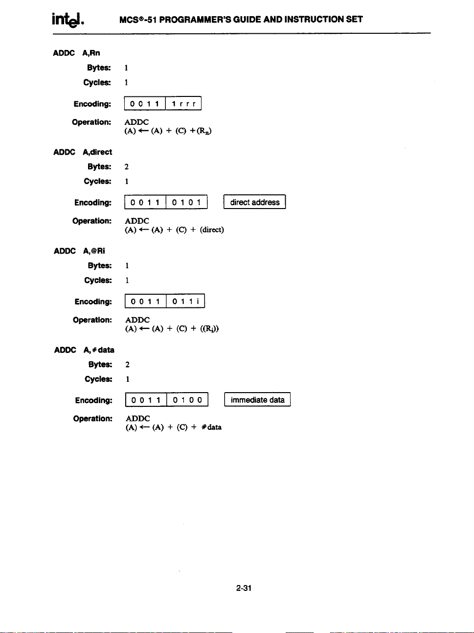
intd.
ADDC A,Rn
Bytes: 1
Cyclm 1
MCS@-51PROGRAMMER’SGUIDE AND INSTRUCTION SET
Encoding: 0011
Operation:
ADDC A,direct
Bytes:
Cycles: 1
Encoding:
Operation: ADDC
ADDC A,@Ri
Bytes: 1
Cycles: 1
Encoding:
Operation:
ADOC A,+dats
Bytes: 2
Cyclesx
Irrr
ADDC
(A) - (A) + (0 +(%)
2
0011
(A) + (A) + (C) + (direct)
0011
ADDC
(A) + (A) + (C) + ((IQ)
0101
Olli
1
1
directaddress
Enooding:
Operation:
0011
ADDC
(A) +- (A) + (C) + #data
0100
immediatedata
I
2-31
Page 62

i~. MCS@-51PROGRAMMER’SGUIDE AND INSTRUCTION SET
AJMP addrll
AbsoluteJultlp
AJMP transfers programexecutionto the indicatedaddress,whichia formedat run-timeby
concatenatingthehigh-orderfivebits of the PC (afier incrementingthe PCtwice),opcodebits
7-5,andthe secondbyteof the instruction. Thedestinationmust thereforebe withinthe same
2K blockof programmemoryas the first byte of the instructionfollowingAJMP.
Example
Bytas
Cycles
The label “JMPADR” is at programmemorylocation0123H.The instruction,
AJMP JMPADR
is at location0345Hand willload the PC with O123H.
.
L
2
Encoding:
Operation:
ANL <dest-byte>, <src-byte>
Funotion:
alO a9 a8 O
AJMP
@’cl+ (m + 2
(PClo.o)+ pageaddress
I.@cal-AND for byte variables
ANL performsthe bitwiselogical-ANDoperationbetweenthe variablesindicatedand storea
the results in the destinationvariable.No flags are affected.
Thetwo operandsallowsix addressingmodecombinations.Whenthe destinationisthe Accu-
mulator, the source can w register,direct, regiater-indirec~or immediateaddressing;when
the destinationis a direct address,the source can be the Accumulatoror immediatedata.
Note:When this instructionis used to modifyan output port, the value usedas the original
port data willbe read fromthe output data latch notthe input pins.
Example:
If the AccumulatorholdsOC3H(11OOUHIB)and registerOholds 55H(O1OIO1O1B)thenthe
instruction,
ANL A,RO
willleave41H (OIOWOOIB)in the Accumulator.
Whenthe destinationis a directly addressedbyte, this instruction willclear combinationsof
bits in SOYRAM locationor hardwareregister. Themaskbytedeterminingthepattern of bits
tobe
clearedwouldeitherbeaconstantcontainedintheinstructionora valuecomputedin
the Accumulatorat run-time.The instruction,
ANL Pl, #Ol110011B
0001 a7 a6 a5 a4
a3 S2 al aO
willclear bits 7, 3, and 2 of output port 1.
2-32
Page 63

in~.
ANL
A,Rn
Bytes:
Cycles:
MCS@-51PROGRAMMER’SGUIDEAND INSTRUCTION SET
1
1
Encoding:
Operation:
ANL A,direct
Bytee:
Cycles:
Encoding:
Operation:
ANL &@Ri
Bytes:
Cyclee:
Encoding:
Operation:
ANL A,#data
Bytes:
Cycles:
0101 Irrr
0101 0101
ANL
(A) ~ (A) A (direct)
1
1
0101
ANL
(A) + (A) A (w))
2
1
Olli
directaddress
Encoding:
Operation:
ANL dire@A
Bytas:
cycles
Encoding:
Operation:
0101
ANL
(A) + (A) A #data
0100
2
1
10101
00101
ANL
(direct)+ (direct) A (A)
immediate date
directaddress
2-33
Page 64

i~. M=@-51 PROGRAMMER’SGUIDE AND INSTRUCTION SET
ANL dire@ #dats
Bytes: 3
Cycles: 2
Encoding:
Operation:
ANL C,<src-bit>
Function:
Description:
ANL C,bit
Bytes:
Cycles:
Encoding:
Operation:
0101 0011 directaddress immediatedata
ANL
(direct)+ (direct) A #data
Logioal-ANDfor bit variables
If the Booleanvalueofthe sourcebit isa logicalOthen clearthe carry flag;otherwiseleavethe
carry flagin its current stste. A slash (“/”) precedingthe operandin the assemblylanguage
indicatesthat the logicalcomplementof the addressedbit is usedas the sourcevaluq
sourcebit itself ¬ affwed. No
otherflsgs are affected.
but the
Onlydirectaddressingis allowedfor the source -d.
Setthe carry flag if, and onlyif, P1.O= 1,ACC. 7 = 1,and OV = O:
MOV C,P1.O
ANL ~ACC.7
ANL C,/OV
;LOADCARRY WITH INPUT PIN STATE
;AND CARRY WITH ACCUM. BIT 7
;AND WITH INVERSEOF OVERFLOWFLAG
2
2
1000
100101 H
ANL
(C) ~ (C)
A (bit)
ANL C,/bit
Bytes:
Cycles:
Encoding:
Operation:
2
.
1o11 0000
ANL
(C) + (C)A 1
=
(bit)
2-34
Page 65

it@l.
CJNE <dest-byte>,<src-byte>,rel
MCS’@-51PROGRAMMER’SGUIDE AND INSTRUCTION SET
Function:
Description:
CJNE A,direct,rel
Bytes: 3
Cycles: 2
Compareand Jump if Not Equal.
CJNEcomparesthe magnitudesofthe fmt two operands,andbranchesif their valuesare not
equal.Thebranch destinationis computedby addingthe signedrelative-displacementin the
last instructionbyte to the PC, after incrementingthe PC to the start of the nextinstruction.
The carry flag is set if the unsignedinteger valueof <dest-byte> is less than the unsigned
integervalueof <src-byte>; otherwise,the carry is cleared.Neither operandis tided.
The first two operandsallowfour addressingmode combinations:the Accumulatormaybe
comparedwithany directlyaddressedbyteor immediateda~ andany indirectRAMlocation
or worldngregister can be comparedwithan immediateconstant.
The Accumulator contains 34H. Register 7 contains 56H. The first instruction in the sequence
CJNE R7,#60H, NOT-EQ
. . . . . ; R7 = 60H.
NOT—EQ: “‘“
setsthecarry flagandbranchestothe instructionat labelNOT-EQ. By testingthecarry flag,
this instructiondetermines whetherR7 is greater or lessthan 60H.
If the data being presentedto Port 1is also 34H,then the instruction,
WAIT: CJNE A,P1,WAIT
clearsthe carry tlag and continueswiththe nextinstructionin sequence,sincethe Accumula-
tor doesequalthe data read fromP1.(If someothervaluewasbeinginputonPl, the program
willloopat this point until the PI data changesto 34H.)
JC
REoLLOw
. . . . . . . .
; IF R7 < &3H.
; R7 > 60H.
Encoding:
Operation:
1o11
(PC) - (PC) + 3
IF (A) <> (direct)
THEN
IF (A) <
THEN
~L~E (c) -1
0101
(PC)+ (PC) + relativeoffket
(direct)
(c)+ o
I ‘ire”addressI EiEl
2-35
Page 66

intel.
CJNE A,4$data,rei
Bytee: 3
Cycles: 2
M&0h51 PROGRAMMERS GUIDE AND INSTRUCTION SET
Encoding:
Operation:
CJNE Rn,#dats,rel
Bytea: 3
Cyclea: 2
Encoding:
Operation:
1o11 0100
(-PC)+ (PC) + 3
IF (A) <> data
THEN
(PC)-
IF (A) < data
THEN
EME (c) -1
(c) + o
1o11 Irrr
(PC) + (Pc) + 3
IF (Rn) <> data
THEN
(PC) + m) +
IF (R@ < data
THEN
(c) + 1
ELSE
(c)+ o
(PC)+
] immediatedats I ! rel. address I
relative offiet
immediate data
I
relativeofiet
EEl
CJNE @Ri,#data,rel
Bytea: 3
Cyclea: 2
Encoding:
Operation:
1o11 Olli
I
(P(2)+ (PC) + 3
IF ((Ri)) <> data
THEN
(PC)
t (PC!)+
IF (@i)) < data
THEN
ELSE (c) -1
(c) + r)
I immediatedate I I rel.addressI
rehztiveoflset
2-36
Page 67

intd.
CLR A
MCS@-51PROGRAMMER’SGUIDE AND INSTRUCTION SET
Function:
Description:
Example:
Encoding:
Operation:
CLR bit
Function:
Description:
Example:
Bytee:
Cyclea:
ecunlulator
Clear A
The Aecunmlatoris cleared(all bits set on zero).No flagsare affeeted.
The A
ccumulatorcontsins5CH (010111OOB).The instruction,
CLR A
will leavethe Accumulatorset to OOH(~
B).
1
1
1110
0100
CLR
(A) + O
bit
Clear
Theindicatedbit is cleared(reset to zero).No otherflagsare atkted. CLRean operateonthe
CSITYtig or any directlyaddressablebit.
Port 1 has previouslybeen written with 5DH(O1O111O1B).The instruction,
CLR P1.2
willleave the port set to 59H (O1O11CK)1B).
CLR C
Encoding:
Operation:
CLR bit
Encoding:
Operation:
Bytea:
cycle=
Bytea:
Cyclea:
1
1
1100 0011
I
CLR
(c)+ o
2
1
1 100 0010
CLR
(bit) + O
I
I bitaddress I
2-37
Page 68

intelo
CPL A
MCS@-51PROGRAMMER’SGUIDEAND INSTRUCTION SET
Function:
Description:
Example:
Enooding:
Operation:
CPL bit
Function:
Deeoription:
Bytes:
Cycles:
Example:
ComplementAccumulator
Eachbit of the Accumulatorislogicallycomplemented(one’scomplement).Bitswhichprevi-
ouslycontaineda oneare changedto a zero and vice-versa.Notlagsare affected.
The Accumulatorcontains5CH(O1O111CX3B).The instruction,
CPL A
willleavethe Accumulatorset to OA3H(101OOO11B).
1
1
1111
0100
CPL
(A) -1 (A)
Complementbit
Thebit variablespecifiediscomplemented.A bit whichhadbeena oneis changedto zeroand
vice-versa.No other flagsare affected.CLR can operate onthe carry or any directlyaddressablebit.
Note:Whenthis instructionisusedtomodifyan output pin,the valueusedas the originaldata
willbe read from the output data latch, not the input pin.
Port 1has previouslybeenwrittenwith 5BH (O1O1I1O1B).The instructionsequence,
CPL C
Operation:
Bytes:
Cycletx
Encoding:
CPL P1.1
CPL P1.2
willleavethe port set to 5BH(O1O11O11B).
1
1
1o11 0011
I
CPL
(c)+ 1 (c)
2-38
Page 69

i~.
CPL bit
Bytes:
Cycles:
MCS@-51PROGRAMMER’SGUIDE AND INSTRUCTIONSET
2
1
Encoding:
Operstion:
1o11
CPL
100’01 EEiEl
(bit)~l(bit)
DA A
Funotion: Decimrd-adjust AccumulatorforAddition
Description: DAA adjuststhe eight-bitvaluein the Accumulatorresultingfromthe earlieradditionoftwo
variables(each in packed-BCDformat),producingtwo four-bitdigits.AnyADD or ADDC
instructionmay have beenusedto perform the addition.
IfA
ccurmdatorbits 3-Oare greaterthan nine (xxxxlOIO-XXXX1I1I), or if the AC tlag is onq
sixis addedto the A
ccunndatorproducingthe properJ3CDdigitin the low-ordernibble.This
internaladditionwouldsetthe carryflagifa carry-outofthelow-orderfour-bitfieldpropagated through all high-orderbits, but it would not clear the carry tlag otherwise.
If the carry tlagis nowseLorif thefour high-orderbitsnow exceednine(101OXXXX-1I1XXXX),
thesehigh-orderbitsare incrementedby six,producingtheproperBCDdigitinthe high-order
nibble.Again,this wouldset thecarry flagif there was a carry-outof the high-orderbits, but
wouldn’tclear the carry. The carry flag thus indicatesif the sum of the originaltwo BCD
variablesis greater than 1120,allowingmultipleprecisiondecimaladdition.OVis not affected.
All of this occurs during the oneinstruction cycle.Essentially,this instructionperformsthe
decimal conversionby addingOOH,06H, 60H, or 66H to the Accurnulator, dependingon
ccurmdatorand P3Wconditions.initial A
Note:DA A cannot simplyconverta hexadecimalnumberin the Accrumdatorto BCD nota-
tion, nor doesDA A applyto decimalsubtraction.
2-39
Page 70

intd. MCS@-51PROGRAMMER’SGUIDEAND INSTRUCTION SET
TheAccumulatorholdsthe value56H(OIO1OI1OB)representingthe packedBCDdigitsofthe
decimalnumber56.Register 3 containsthe value67H (0110011lB)representingthe packed
BCDdigits ofthe decimalnumber67.The carry flag is set. The instructionsequence.
ADDC A,R3
DA A
wdl first performa standard twos-complementbinary addition, resultingin the value OBEH
(10111110)in the Accumulator.The carry and auxiliarycarry flagswillbe cleared.
The Decimal Adjust instruction will then alter the Accumulator to the value 24H
(OO1OO1OOB),indicatingthe packedBCDdigitsofthe decimalnumber24,the low-ordertwo
digitsofthe decimalsum of 56,67, and the carry-in.The carry tlagwillbeset bythe Decimal
Adjustinstruction,indicatingthat a ddnal overflowoccurred.The true sum 56,67, and 1is
124.
BCD variablescan beincrementedor decrementedbyaddingOIHor 99H.If the Accumulator
initiallyholds30H(representingthe digitsof 30decimal),then the instructionsequence,
Bytes
Cycles:
Encoding:
Operstion:
ADD
DA A
willleave the carry set and 29H in the Accumulator,since 30 + 99 = 129.The low-order
byteof the sumcan be interpretedto mean 30 – 1 = 29.
1
1
DA
-contentsof Accumulatorare BCD
IF
IF
A#99H
1101 0100
[[(A3-13)>91 V [(AC) = 111
THEN(A34)- (A343)+ 6
AND
[[(A7-4)> 9] V [(C) =
THEN (A74) - (A74) + 6
111
2-40
Page 71

in~.
DEC byte
Function: Decrement
Description:
Exampte:
DEC A
Bytes: 1
Cyclx 1
MCS”-51 PROGRAMMER’SGUIDEAND INSTRUCTION SET
variableindicatedis decrementedby 1.An originalvalueofOOHwillunderilowtoOFFH.
The
No flags are affected. Four operandaddressingmodes are allowed:accumulator,register,
&r@ or register-indirect.
Note: When this instruction is used to modifyan output port, the valueused as the original
port data willbe read from the outputdata latch, not the input pins.
Register Ocontains7FH (0111111IB). Internal RAM locations7EH and 7FH containOOH
and 40H, respectively.The instructionsequence
DEC @RO
DEC RO
DEC @RO
willleaveregisterOset to 7EH and internal RAM locations7EHand 7FH set to OFFHand
3FI-I.
Encoding: 0001 0100
Operation:
DEC
(A) - (A) – 1
DEC Rn
Bytes: 1
cycles: 1
Encoding: 0001
Operation:
DEC
(Rn) + @l) – 1
lrrr
241
Page 72

i~. MCS@-51PROGRAMMER’SGUIDE AND INSTRUCTION SET
DEC direct
Bytes:
Cycles:
2
1
Encoding:
Operation:
0001 0101
DEC
I
directaddress
(direct)- (direct) – 1
DEC @Ri
Bytes:
Cycles:
Encoding:
Operation:
1
1
10001 I Ollil
DEC
(w)) -((N)) – I
DIV AB
Function:
Description:
Divide
DIV AB divideathe unsignedeight-bitintegerin the Accumulatorby the unsignedeight-bit
integer in register B. The Accumulatorreceivesthe integerpart of the quotient;register B
receivesthe integerremainder.The carry snd OVtlagswill be cleared.
Exception:ifB had originallycontainedOOH,the valuesreturned in the Accumulatorand B-
register willbe undefinedand the overflowflag willbe set. The carry tlag is clearedin any
case.
Example: TheAccumulatorcontains251(OFBHor 11111011B)andBcontains 18(12Hor OOO1OO1OB).
The instruction,
Bytes: 1
Cycles: 4
Enooding:
Operation:
DIV AB
willleave 13in the Accumulator(ODHor OOOO11O1B)and the value 17 (lIH or OOO1OOO1B)
in B, since251 = (13X 18) + 17.Carry and OVwillboth be cleared.
1000 0100
I
DIV
(A)15.8
~)74 - (A)/@t)
2-42
Page 73

in~.
DJNZ <byte>, <rel-addr>
MCS@-51PROGRAMMER’SGUIDE AND INSTRUCTION SET
Function: DecrementandJumpif Not
Description: DJNZ decrementsthe location indicatedby 1,and branchesto the addressindicatedby the
=0
secondoperandif the resultingvalueis not zero.An originalvalueof OOHwillunderflowto
OFFH.No tlagsare at%cted.The branch destinationwouldbecomputedbyaddingthe signed
relative-displacementvalueinthe last instructionbyteto the PC, after incrementingthe PC to
the first byte ofthe followinginstruction.
The location decreznentedmaybe a registeror directlyaddressedbyte.
Note:When
thisinstructionis used to modfi an outputport, the valueused as the original
port data will be read from the output data latch, notthe input pins.
Example: Internal RAM locations40H, 50~ and 60H containthe valuesOIH,70H,and 15H,respec-
tively.The instructionsequence,
DJNZ 40H,LABEL-1
DJNZ 50H,LABEL-2
DJNZ 60H,LABEL-3
willcauseajumpto the instructionat labelLABEL-2 withthe valuesOOH,6FH,and 15H in
the three W locations The firstjump was nottakenbecausethe result waszero.
This instructionprovideaa simplewayof executinga programloopa givennumberof times,
or for addinga moderatetime delay (from2 to 512machinecycles)with a singleinstruction.
The instructionsequence,
MOV R2,#8
TOOOLE: CPL P1.7
DJNZ
R2,TOOGLE
will toggleP1.7 eight times, causingfour output pukes to appear at bit 7 of output Port 1.
Each pulsewill last three machinecycles;twofor DJNZ and oneto alter the pin.
DJNZ Rn,rel
Bytee: 2
cycles: 2
Encoding:
Operation:
1101
I
DJNZ
(PC!)- (PC) + 2
m) -(w – 1
w ~~~ 0 or (I@ < t)
11’”1 EEl
(PC)+ (PC)+ rd
2-43
Page 74

int&
DJNZ direct@
Byte=
Cycles
MCS”-51 PROGRAMMER’SGUIDEAND INSTRUCTIONSET
3
2
Encoding:
Operation:
1101
DJNZ
0101
I ‘irw’addressI EiEl
(PC)+ (PC) + 2
(direct)+ (direct) – 1
IF (direot) >0 or (direct) <0
THEN
(PC)-(PC) + ml
INC <byte>
Function:
Description: INC incrementsthe indicatedvariableby 1.An originalvalueofOFFHwill overflowtoOOH.
Incmsnent
No figs are affected.Threeaddressingmodesareallowed:register,direct,or register-indirect.
Note.”When this instructionis used to modifyan output port, the value used ss the original
port data willbe read from the outputdata latch, not the inputpins.
Exsmple: RegisterOcontains7EH (01111111OB).InternalRAM locations7EHand 7FHmntain OFFH
and 40H, respectively.The instructionsequence,
INC @RO
INC RO
INC @RO
willleaveregisterOset to 7FHand internalRAMlocations7EHand7FH holding(respectively) (XIHand 41H.
INC A
Bytes: 1
cycles: 1
Encoding:
Operstion:
0000 0100
INC
(A) + (A) + 1
2-44
Page 75

i~e
INC Rn
Bytes:
cycles
M=”-51 PROGRAMMER’SGUIDE AND INSTRUCTION SET
1
1
Encoding:
Operation:
INC direct
Cycles:
Encoding:
Operation:
INC @Ri
Cycles:
Encoding:
Operation:
INC DPTR
Function:
Description:
Bytee:
Bytes:
0000 Irrr
INC
m)+ w) + 1
2
1
0000 0101
directaddress
1
INC
(direct)~ (direct) + 1
1
1
0000 Olli
INC
(m)) + (m)) + 1
IncrementDsta Pointer
Incrementthe id-bit data pointer by 1. A id-bit increment(modulo216)is performed;an
overflowof the low-orderbyteof the data pointer (DPL) fromOFFHto COHwill increment
the high-orderbyte (DPH). No tlsgs are sfkted.
Example:
Bytes:
Cycle=
Encoding:
Operation:
Thisis the only id-bit register whichcan be incremented.
RegistersDPH and DPL contsin 12Hsnd OFEH,respectively.The instructionsequence,
INC DPTR
INC DFTR
INC DPTR
willchsngeDPH and DPL to 13Hsnd OIH.
1
2
1o1o 0011
INC
(DPTR)- (DFITl) + 1
245
Page 76

i~.
JB bityrei
MCS@-5fPROGRAMMER’SGUIDEAND INSTRUCTION SET
Function:
Description:
Jumpif Bit set
If the indicated bit is a one,jump to the addreasindicat@ otherwiseproceedwith the next
instruction.Thebranch destinationis computedbyaddingthe signedreistive-displscem
the third instructionbyte to the PC, after incrementingthe PC to the fnt byte of the next
instruction.The
The data
present at inputport 1is 11OO1O1OB.The Accumulatorhoids56 (O1O1O11OB).The
instructionsequence,
JB P1.2,LABEL1
JB ACC.2,LABEL2
willcauseprogram executionto branch to the instructionat label LABEL2.
Bytes:
Cycierx
Encoding:
Operstion:
3
2
JB
0010
1004 EEzEEl EizEl
(PC)+ (PC)+
IF (bit) = 1
THEN
(PC) +- (PC) + rel
JBC bitrei
Function: lump if Bit issetandClearbit
Description:
If the indicatedbit is one,branch to the addressindicated;otherwiseproceedwith the next
instruction.17re
ed by addingthe signedrelative-displacementin the third instructionbyte to the PC, after
incrementingthe PC to the tlrst byte of the nextinstruction.No flagsare affected.
ent in
bit tested k nor modified. No tlags are affected.
3
bit wili not be cleared ~~itis already a zero. The branchdestinationis comput-
Exempie:
Note:When this instructionis used to test an outputpin, the valueusedas the originaldata
willbe read from the output data latch, notthe input pin.
The
Accumulatorholds56H(01010110B).The instructionsequence,
JBC ACC.3,LABELI
3BC ACC.2,LABEL2
willcauseprogram executionto continueat the instructionidentifiedby the label LABEL2,
withthe Accumulatormodifiedto 52H (OIO1OO1OB).
2-46
Page 77

M=”-51 programmers GUIDE AND INSTRUCTION SET
Encoding:
Operation:
JC rel
Function:
Daacription:
Bytes:
Cycles:
Exsmple:
Bytes
cycles:
3
2
I“” ”’l” ”””1 DEEl EiEiEl
JBc
(PC) - (PC) + 3
IF (bit) = 1
THEN
(bit)* O
(PC)~ (PC) + rel
Jump if Carryis set
If the carry flag is set, branch to the addreas indicated; otherwiseproceed with the next
instruction.Thebranchdestinationis computedbyaddingthe signedrelative-displacementin
the secondinstructionbyteto the PC, after incrementingthe PC twice.No flagsare afkted.
The carry flagis clesred.The instructionsequence,
JC LABEL1
CPL C
JC LABEL2
willset the carry and causeprogramexecutionto continueat the instructionidentifiedby the
labelLABEL2.
2
2
Encoding:
Operation:
0100 0000
JC
(PC)+ (PC)+ 2
IF (C) = 1
THEN
(PC)~ (PC) + rel
=
2-47
Page 78

i@.
JMP @A+DPIR
MCS@-51PROGRAMMER’SGUIDEAND INSTRUCTION SET
Function:
Bytex
Oycies:
Encoding:
Opersliorx
]umpindirect
Addthe eight-bitunsignedcontentsofthe Accurnulator withthe sixteen-bitdata pointer,and
loadthe resultingsumto the programcounter.Thiswillbethe addressforsubsequentinstruction fetches.Sixteen-bitaddition is performed(modrdo216):a camy-outfrom the low-order
eight bits propagatesthrough the higher-orderbits. Neither the Accumulator nor the Data
Pointer is altered.No tlags are affected.
An evennumberfromOto 6 isin the Accumulator.Thefollowingsequenceofinstructionswill
branch to oneof four AJMP instructionsin a jump table starting at JMP-TBL:
MOV
JMP-TBL:
If the Accumulatorequals 04H when starting this sequence,executionwilljump to label
LABEL2.Rememberthat AJMP is a two-byteinstruction,so the jump instructionsstart at
everyother address.
1
2
10111 00111
JMP
W)+ (A) +
JMP
AJMP LABEL.O
AJMP LABEL1
AJMP LABEL2
AJMP LABEL3
WW
DPTRj#JMP-TBL
@A+DPTR
2-48
Page 79

JNB bi~rel
MCS@-51PROGRAMMER’SGUIDE AND INSTRUCTION SH
Function:
Jump if Bit Not set
If the indicatedbit is a zero,branchto the indicatedaddress;otherwiseproceedwiththe next
instruction.The branchdestinationis computedby addingthe signedrelative-displacementin
the third instructionbyte to the PC, after incrementingthe PC to the first byte of the next
Example:
instruction. The
Thedata presentat inputport 1is 11W101OB.The Accumulatorholds56H (01010110B).The
bit tested is not modt~ed. No flagsare affected.
instructionsequence,
JNB P1.3,LABEL1
JNB ACC.3,LABEL2
willcause programexecutionto continueat the instructionat label LABEL2.
Bytes:
Cycles:
Encoding:
Operation:
3
2
0011
100001 LGzEl EEl
JNB
$W:)y; +
3
THEN (PC)t (PC) + rel.
JNC rel
Function: Jump if Carry not set
Description:
If the carry tlag is a zero, branch to the addreasindicated;otherwise
instruction.The branch destinationiscomputedby addingthe signedrelative-displacementin
the secondinstructionbyte to the PC, after incrementingthe PC twice to point to the next
inatruetion.The carry tlag is not moditled.
Example: The carrytlagis set. Theinstructionsequence,
proceedwith the next
JNC LABEL1
CPL C
JNc LABEL2
willclear the carry and causeprogramexecutionto continueat the instructionidentitkd by
the labelLABEL2.
Bytes 2
Cycles: 2
Encoding:
Operation: JNC
0101
(PC) - (PC) + 2
IF (C) = O
100001 -
THEN (PC)t (PC) + rel
2-49
Page 80

i~. MCS@-51PROGRAMMER’SGUIDE AND INSTRUCTION SET
JNZ rel
Encoding:
Operation:
JZ rel
Daaoription:
Function:
Example:
Bytea:
Cyclea:
Function:
Jump if AccumulatorNot Zero
If any bit ofthe Accum
ulatorisa one,branchto the indicatedaddress;otherwiseproceedwith
the next instruction.The branch destination is computedby adding the signedrelativedisplacement in the second instructionbyte to the PC, after incrementingthe PC twice. The
Accumulatoris not modified.No tlags are affected.
The AccumulatororiginallyholdsOOH.The instructionsequence,
JNZ LABEL1
INC A
JNZ LAEEL2
willset the Accumulatorto OIHand continueat label LABEL2.
2
2
0111
JNz
10’001 EiEl
(PC)+ (PC) + 2
IF (A) # O
THEN (PC)~ (PC) + rel
Jump if AccumulatorZero
If all bits ofthe Accumulatorarezero,branch tothe addressindica@ otherwiseproceedwith
the
next instruction.The branch destination is computedby addingthe signedrelative-dis-
placement in the secondinstructionbyte to the PC, after incrementingthe PC twice. The
Accumulatoris not modified.No flagsare affected.
The AccumulatororiginallycontainsOIH.The instructionsequen~
Bytea:
Cycles:
E“ncodirrg:
Operation:
JZ LABELI
DEC A
JZ LABEL2
willchange the Aec.umulator to OOHand causeprogramexeeutionto continueat the instruction identifiedbythe label LABEL2.
“
.4
2
0110
I
Jz
(PCJ)+ (w)+
0000
2
rel. addreee
[
IF (A) = O
THEN (PC) t @C) + rel
2-50
Page 81

in~. M=”-51 programmers GUIDEAND INSTRUCTION SET
LCALL addr16
Function:
Description:
Example:
Bytes:
Cycles:
Encoding:
Operation:
Longcall
LCALLcalls a subroutineIooatedat the indicatedaddress.The instructionaddsthree to the
programcounter to generatethe addressof the next instruction and then pushesthe Id-bit
result ontothe stack (lowbyte first), incrementingthe StackPointer by two.The high-order
andlow-orderbytesofthe PC are thenloaded,respectively,withthe secondandthird bytesof
the LCALLinstruction.Programexeoutionrxmtinueswith the instructionat this address.The
subroutinemaythereforebeginanywhereinthe full 64K-byteprogrammemoryaddressspace.
No ilags are affeeted.
InitiallytheStackPointer equals07H.The label“SUBRTN”is assignedto programmemory
location 1234H.After exeoutingthe instruction,
LCALL SUBRTN
at location0123H,the Stack Pointerwillcontain09H, internal IL4MIccations08Hand 09H
willcontain26Hand OIH,and the PC willcontain 1234H.
3
2
0001 0010
I addr’’-add’ I EEEiEl
LCALL
(PC) + (PC) + 3
(SP)+ (SP) + 1
((sP)) - (PC74)
(SP)- (SP) + 1
((sP)) - (PC15.8)
(PC)~ addr15~
UMP addr16
Function:
Description:
Example:
Cycles:
Enooding:
operation:
Long Jump
LJMPcausesan unconditionalbranchto the indiestedaddress,byloadingthe high-orderand
low-orderbytes of the PC (respectively)with the second and third instruction bytes. The
destinationmay therefore be anywherein the full 64K program memoryaddress sparx. No
flagsare affected.
Thelabel“JMPADR” is assignedto the instructionat programmemorylocation1234H.The
instruction
LJMP JMPADR
at location0123Hwillload the programcounterwith 1234H.
2-51
Page 82

i~. M=@-51 PROGRAMMER’SGUIDEAND INSTRUCTION SET
MOV <dest-byte>,<erc-byte>
Function:
Oeacription:
Example:
MOV A,Rn
Bytes:
Cycles:
Encoding:
Operation:
*MOV A,direct
Bytes:
Cycles:
Movebytevmiable
Thebyte
variableindicatedby the secondoperandis copiedintothe locationspecifiedbythe
first operand.The sourcebyte is not affeeted.No other register or flag is at%eted.
This is by far the mmt flexibleoperation.Fifteen combinationsof source and destination
addressingmodesare allowed.
Internal RAM location 30H holds 40H.The valueof RAM location40H is 10H.The data
prcaentat input port 1 is 11OO1O1OB(OCAH).
MOV RO,#30H ;RO< = 30H
MOV A,@RO
MOV R1,A
MOV B,@Rl
MOV @Rl,Pl
MOV P2,PI
leavesthevalue30H in registerO,40Hin boththe Aecum
;A < = 40H
;Rl < = 40H
;B < = 10H
;RAM (4X-I)< = OCAH
;P2 #OCAH
ulator andregister 1,10Hitsregister
B, and OCAH(11OO1O1OB)bothin RAM Ioeation40H and output on port 2.
1
1
1110
lrrr
MOV
(A)+ (RIO
2
1
Encoding:
Operation:
MOV~ACC
1110 0101
MOV
(A)+ (direct)
ie not a valid instruction.
directaddress
2-52
Page 83

intd.
MOV A,@Ri
Bytes:
Cycles:
MCS@-51PROGRAMMER’SGUIDE AND INSTRUCTION SH
1.
1
Encoding:
Operation:
MOV A,#data
Bytes:
Cycles:
Encoding:
Operation:
MOV Ftn,A
Bytes:
Cycles:
Encoding:
Operation:
MOV Rn,direot
Bytee:
Cyclea:
1110
Olli
MOV
(A) - (~))
2
1
0111
0100
MOV
(A) + #data
1
1
I 1111 I Irrrl
MOV
~) t (A)
.
L
2
immediatedata
I
Encoding:
Operation:
MOV Rn,#data
Bytes:
cycles:
Encoding:
Operation:
1010
I
Ilr’rl -
MOV
(I@ + (direct)
.
1
0111 lrrr
MOV
(R@- #dsts
immediatedata
2-53
Page 84

irrtd.
MOV directJl
Bytetx
Cycle$x
M~@-51 PROGRAMMER’SGUIDE AND INSTRUCTION SET
2
1
Encoding:
Operation:
MOV dire@Rn
Bytes:
Cyciee:
Encoding:
Operation:
MOV directjdirect
Bytw 3
Cycie= 2
Encoding:
Operation:
MOV direct@Ri
Bytes: 2
Cycles: 2
1111 0101
MOV
(direct)- (A)
2
2
1000
Irrr
MOV
(direct)+ (lb)
1000 0101
I
MOV
(direct) +- (direct)
directaddress
directaddress
dir.addr. (src) dir.addr.(dest)
I
Encoding:
Operation:
MOV direc$xdats
%yte= 3
Cycle= 2
Encoding: 0111
Operation:
1000 Olli
I
MOV
(MM) + (w))
0101
MOV
(direct) + #date
directaddress immediatedata
2-54
I
Page 85

intd. MCS@-51PROGRAMMEWSGUIDE AND INSTRUCTIONSET
MOV @Ri&
B-
cycles:
.
1
1
Encoding:
Operation:
1111
MOV
Olli
(@i)) + (A)
MOV @Ri,direct
Bytes:
Cycles:
Encoding:
Operation:
2
2
llOIOIOllil
MOV
I directaddr. I
(@i)) + (direct)
MOV @Ri,#data
Bytes:
Cycles:
Encoding:
Operation:
2
.
1
0111 Olli
MOV
I
immediate data
((RI)) + #data
MOV <cleat-bit>, <erc-bit>
Function: Move
Description: The Booleanvariableindicatedbythe secondoperandis copiedinto the locationspecitkdby
bitdata
the first operand.One of the operandsmust be the carry flag;the other may be any directly
addressablebit. No other registeror flag is affected.
Example: The carry tlag is originallyset.The data present at input Port 3 is 11OOO1OIB.The data
previouslywrittento outputPort 1is 35H (03110101B).
MOV P1.3,C
MOV C,P3.3
MOV P1.2,C
will
leavethecarryclearedand changePort 1to 39H(OO111OO1B).
2-55
Page 86

I I
int& M=@-51 PROGRAMMER’SGUIDE AND INSTRUCTIONSET
MOV C,blt
Bytes:
Cycles:
2
1
Enooding:
Operstion:
MOV bi&C
Bytes:
Cycles:
Enooding:
Operstion:
MOV DPTR,#dsts16
Function:
Description:
Example:
Bytesx
Cycles:
1o1o
MOV
(~+(bit)
.
L
1“0’01 EiEl
2
1001
1“0’01 E
MOV
(bit)+ (C)
LoadData Pointer with a Id-bitconstant
The Data Pointer is loadedwith the Id-bit constant indicated.The id-bit constant is loaded
into the secondand third bytesof the instruction. The secondbyte (DPH) is the high-order
byte,whilethe third byte (DPL) holdsthe low-orderbyte.No tlagsare atTeeted.
Thisis the only instructionwhichmovea16 bits of tits at once.
Theinstruction,
MOV DPTR,# 1234H
willloadthe value 1234Hintothe Data Pointer:DPH willhold12Hand DPL willhold 34H.
3
.
L
Encoding:
Operation:
1001 0000
immed.dsts15-6
I
MOV
(DPTR)~ #data154
DPH ❑ DPL + #<S15.8❑ #data73
2-56
immed.data7-O
I
Page 87

intd.
MCS@-51PROGRAMMER’SGUIDE AND INSTRUCTION SET
MOVC A,@A+<baas-reg>
Function:
Description:
Example:
MOVC ~@A+
Bytes:
Cycles:
MoveCodebyte
The MOVCinatmctionsload the Accumulatorwith a oodebyte, or constantfrom program
memory.Theaddressofthe bytefetchedis thesumof the originalunsignedeight-bitAccumu-
lator contents and the contentsof a sixteen-bitbase register, whichmay be either the Data
Pointeror the PC. In the latter case, the PC is incrementedto the addressof the following
instructionbeforebeingadded with the Accumulator;otherwis
e the base register is not altered. Sixteen-bitaddition is performedso a carry-out from the low-ordereight bits may
propagatethroughhigha-order bits. No flagsare affected.
A valuebetweenO and 3 is in the Accumulator.The followinginstructionswilltranslate the
valuein the Accumulatorto one of four valuesdefimedby the DB (definebyte)directive.
REL-PC: INC A
MOVC A,@A+PC
RET
DB
66H
DB 77H
DB
DB
88H
99H
If the subroutineis calledwith the Accumulatorequalto OIH, it willreturn with 77H in the
Auxmmlator.The INCA beforethe MOVCinstructionis neededto “get around” the RET
instructionabovethe table. If severalbytesof codeseparated the MOVCfrom the table, the
correspondingnumberwouldbeadded to the Accumulatorinstead.
DPTR
1
2
Encoding:
Operation:
MOVC A,@A +
Bytes:
Cycles:
Encoding:
Operation:
11001 10011 I
MOVC
(A)+ ((A) + (D~))
Pc
1
2
1000
0011
MOVC
(PC)+ (PC) + 1
(A)- ((A) + (PC))
2-57
Page 88

int&
MOVX <dest-byte>, <sin-byte>
Function: MoveExternal
Deaoription: The MOVX
Example:
MCS@-51PROGRAMMER’SGUIDE AND INSTRUCTION SET
memory,hencethe “X” appendedto MOV.There are two types of instructions,differingin
whetherthey providean eight-bitor sixteen-bitindirect address to the externrddata RAM.
In the first typq the contents of ROor R] in the current registerbank providean eight-bit
address multiplexedwith data on PO.Eight bits are sufficientfor external 1/0 expansion
decodingor for a relativelysmall RAM array. For somewhatlarger arrays, any output port
pins can be used to output higher-orderaddressbits. These pins would be controlledby an
outputinstructionprecedingthe MOVX.
In the secondtypeofMOVXinstruction,the Data Pointer generatesa sixteen-bitaddress.P2
outputsthehigh-ordereight addressbits (the contentsof DPH) whilePOmultiplexesthe loworder eightbits (DPL) with data. The P2 SpecialFunction Registerretainsits previouscontents whilethe P2 ouQut buffersare emittingthe contents of DPH. This form is faster and
more efticientwhenaccessingvery large data arrays (up to 64K bytes),since no additional
instructionsare neededto set up the output ports.
It is possiblein somesituations to mix the two MOVX types.A large R4M array with its
high~rder addresslinesdrivenby P2 can be addressed via the Data Pointer,or with codeto
outputhigh-orderaddress bits to P2 followedbya MOVXinstructionusingROor RI.
An external256byte RAM using
I/Oflimer) is connectedto the 8051Port O.Port 3 providescontrol linesfor the external
W. Ports 1 and 2 are used for normal 1/0. Registers O and 1 contain 12H and 34H.
Location34Hof the extemsJ RAM holdsthe value 56H. The instructionsequence,
instructionstransfer data betweenthe Accumulatorand a byteof exa data
multiplexedaddress/&talines(e.g.,anMel 8155UM/
MOVX A@Rl
MOVX @RO,A
copiesthe value56H into both the Accumulatorand external RAM location12H.
2-58
Page 89

i~o
MOVX &@Ri
Bytes: 1
Cycles: 2
Encoding: 1110 OOli
M=@-51 PROGRAMMER’SGUIDEAND INSTRUCTION SET
Operation:
MOVX
MOVX @Ri,A
MOVX @DPIR#l
A@DPIR
Bytes:
Cycles:
Encoding:
Operation:
Bytes:
Cycles:
Encoding:
Operation:
Bytes: 1
cycles: 2
Encoding:
MOVX
(A) - (~))
1
2
1110 0000
1
2
1111
MOVX
1111 0000
OOli
Operation: MOVX
(DPTR) - (A)
2-59
Page 90

i~e MCS”-51 PROGRAMMER’SGUIDE AND INSTRUCTION SET
MUL AB
Multiply
Deeoriptiors:
Example
Bytes:
Cycles:
MUL AB multipliesthe unsignedeight-bit integersitsthe Accumulator and registerB. The
Iow-orderbyteof the sixteen-bitproduct is leftin the Accumulator,andthe high-orderbytein
B. If the product is greaterthan 255 (OPPH)the ovcrtlowflag is set; otherwiseit is cleared.
The carry fiag is alwayscleared.
Originallythe Accumulatorholdsthe value80(50H).RegisterB holdsthe value 160(OAOH).
The instruction,
MuLAB
willgivethe product 12,S00(3200H),soB is changedto 32H(OO11OO1OB)and the Accumula-
tor is cleared.The overflowflagis set, carry is cleared.
1
4
Encoding:
Operation:
NOP
Description:
Encoding:
Function:
Example:
Bytes
Cycles:
I 101 OIO1OOI
MUL
(A)74 + (A) X (B)
(B)15-8
No Operation
Executioncontinuesat the followinginstruction.Other than the PC, no registersor flagsare
affected.
It is desiredto producea low-goingouQut pulseonbit 7 of Port 2 lastingexactly5cycles.A
simpleSETB/CLRsequencewouldgeneratea one-cyclepulse,so four additionalcyclesmust
be inserted. This may be done (ssauming no interrupts are enabled) with the instruction
SeqUenee,
CLR P2.7
NOP
NOP
NOP
NOP
SETB P2.7
1
1
000010000
Operation:
NOP
(PC)+ (-PC)+ 1
2-00
Page 91

in~.
MCS@-51PROGRAMMER’SGUIDE AND INSTRUCTION SET
ORL <dest-btie> <src-byte>
Funotion:
Example:
ORL &Rn
Cycles:
Bytes:
Logicsl-ORfor byte variables
ORL performsthe bitwiselogical-ORoperationbetweenthe indicatedvariables,storingthe
results in the destinationbyte.No flagsare affected.
The twooperandsallowsixaddressingmodecombinations.Whenthedestinationis the Accu-
mulator, the source can use register, direct, register-indirect,or immediateaddressing;when
the destinationis a direct addreas,the sourcecan be the Accumulatoror immediatedata.
Note.-When this instructionis used to modifyan output port, the valueused as the original
port dats will be resd fromthe output data latch, not the input pins.
If the Accumulatorholds OC3H(I1OOOO1IB)and ROholds 55H (O1O1O1O1B)then the instruction,
ORL A,RO
will leavethe Accumulatorholdingthe valueOD7H(110101llB).
When the destinationis a directlyaddreasedbyte,the instructioncan set combinationsofbits
in any RAM location or hardwareregister. The pattern of bits to be set is determinedby a
maskbyte,whichmaybeeithera constantdatavalueinthe instructionor a variablecomputed
in the Aecunndatorat rim-time.The instruction,
ORL P1,#OOllOOIOB
willset bits 5,4, and 1of output Port 1.
1
1
Encoding:
Operstion:
0100
lrrr
ORL
(A) +- (A) V K)
2-61
Page 92

i~e M=a-slPROGRAMMER’SGUIDEANDINSTRUCTION SET
ORL &direct
Bytes:
Cycles:
2
1
Encoding:
Operation:
ORL &@Ri
Bytes:
Cycles:
Encoding:
Operation:
ORL A,#dets
Bytes:
Cycles:
Encoding:
Operation:
ORL direct,A
Bytes:
Cyclea:
1010010101 I
ORL
(A)+ (A) V (direct)
1
1
0100
Olli
2
1
Iolool O1oo1
ORL
(A) - (A) V #dsts
1
directaddress
immediatedata
Encoding:
Operation:
ORL direcQ*data
Bytes: 3
Cycles: 2
Encoding: 0100
Orwstion: ORL
0100
0010
ORL
(direct)~(direct) V (A)
0011
(direct)+ (direct) V #data
I
directaddress
EEEl
2-62
immediate date
I
Page 93

in~.
ORL C,<src-bit>
MCS@-51PROGRAMMER’S GUIDE AND INSTRUCTION SET
Function:
Description:
Example:
ORL C,bit
Cycles:
Encoding:
Operation:
ORL C,/bit
Cycles:
Encoding:
Operation:
Bytes:
Bytes:
Logical-ORfor bit variables
*t the carry flagif the Booleanvalue is a logical 1; leave the carry in its current state
otherwise. A slash (“/”) precedingthe operand in the assemblylanguageindicatesthat the
logicalcomplementofthe addressedbit is usedas the sourcevalue,but the sourcebit itselfis
not at%cted.No other tlags are afkcted.
Setthe carry flag if and onlyifP1.O = 1, ACC. 7 = 1,or OV = O:
MOV CPI.O
ORL C,ACC.7 ;OR CARRY WITH THE ACC.BIT 7
;LOADCARRYWITH INPUT PIN P1O
ORL Wov ;OR CARRYWITH THE INVERSEOF OV.
2
2
0111
2
IOO1OI EEl
.
1010
I
100001 EEEl
ORL
(c)+ (c) v
@=)
2-63
Page 94

i~.
POP direot
M~eI-51 programmers GUIDE AND INSTRUCTION SET
mrsctiom
Example:
Bytea:
Cycla$s
Encoding:
Operation:
PUSH direct
Popfrom stack.
The contentsof the internal RAM locationaddressedby the Stack Pointer is read, and the
Stack Pointer is decrementedby one. The valueread is then transferred to the directly addressedbyte indicated.No flagsare affected.
The Stack Pointer originally contains the value 32H, and internal RAM locations 30H
through32Hcontainthe values20H, 23H,and OIH,respectively.Theinstructionsequen~
POP DPH
POP DPL
willleavethe StsckPointer equalto the value30Hand the Data Pointer setto 0123H.At this
pointthe instruction,
POP SP
willleavethe Stick Pointer set to 20H. Notethat in this specialcase the Stack Pointer was
*remented to 2FH beforebeingloadedwith the valuepopped
2
2
1101 0000
I
directaddress
(20H).
POP
(direct)+ ((sP))
(SP)4-(SP) – 1
Function:
Description:
Bytes:
Cycletx
Enooding:
Operation:
push onto stack
TheStackPointeris incrementedbyone.Thecontentsof the indicatedvariableis then copied
into the internalRAM locationaddressedbythe StackPointer.Otherwiseno flagsare affected.
On entaing an interrupt routinethe StackPointercontains09H.The Data Pointer holdsthe
valueO123H.The instructionsequence,
PUSH DPL
PUSH DPH
willleave the Stack Pointer set to OBHand store 23H and OIH in internal FL4Mlocations
OAHand OBH,respectively.
2
2
1100
0000
directaddreaa
I
PUSH
(SP)+ (SP) + 1
((SP))- (direct)
2-04
Page 95

int&
RET
M~tV-51 PROGRAMMER’SGUIDEANDINSTRUCTIONSET
Function:
Description:
Example:
Encoding:
Operation:
RETI
Function:
Description:
Exemple:
Bytm
cycles:
Return tlom subroutine
RET popsthe high-and low-orderbytesofthe PC successivelyfromthe staclGdecrementing
the Stack Pointerbytwo. Program executioncontinuesat the resultingaddress,generallythe
instructionimmediatelyfollowingan ACALLor LCALL.No tlagsare affected.
The StackPointeroriginallycontainsthe valueOBH.Internal RAMlocationsOAHand OBH
containthe value-a23H and OIH, respectively.The instruction,
RET
will leave the Stack Pointer equal to the value 09H. Program executionwill continue at
Ioeation0123H.
1
2
10010100101
RET
(Pc~~-s)+- ((sP))
(SP)+(SP) – 1
(PC74) + ((sP))
(SP)+ (SP) -1
Return from interrupt
RETI popsthe high-and low-orderbytesof the PC successivelyfromthe stack, and reatores
the interrupt logicto accept additional interrupts at the same priority levelas the onejust
processed.The StackPointer is left decrementrdby two. No other registersare aik%sd; the
PSWis not automaticallyrestored to its pre-interruptstatus. Programexecutioncontinuesat
the resultingaddress,whichis generallythe instructionimmediatelyafter the pointat which
the interrupt requestwas detected.
the RETI instructionis executed, that one instructionwill be executedbeforethe pending
interrupt is processed.
The Stack Pointer originallycontains the valueOBH.An interrupt was detectedduring the
instruction endingat location 0122H.Internal RAM locationsOAHand OBHcontain the
values23Hand OIH, reapeotively.The instruction,
Ifa lower-or same-level interrupthadbeenpendingwhen
Bytes:
Cyclee:
Encoding:
Operation:
RETI
wiltleavethe StackPointer equat to O$IHand return program executionto locationO123H.
1
2
10011 I 00101
(PCls.s)+ ((sP))
(sP)+ (SP) -1
(PC74) + ((sP))
(SP)-(SP) -1
2-65
Page 96

intd. M=”-51 PROGRAMMER’SGUIDE AND INSTRUCTION SET
RL A
Function:
Description:
Encoding:
Operation:
RLC A
Description:
Example:
Bytes:
Cycle=
Function:
Example:
Rotate Aecurn
ulator Left
Theeightbits in the Aeeurmdatorare rotated onebit to the left. Bit 7 is rotated into the bit O
position.No flagsare akted.
The Aeeumulatorholdsthe valueOC5H(11OQO1O1B).Theinstruction,
RLA
leavesthe Accumulatorholdingthe value 8BH(1OOO1O11B)withthe carry unaffected.
1
L
0010 0011
RL
1)- (An) n = O – 6
(~ +
(AO)+ (A7)
Rotate Accum
ulator L-et?throughthe Carry flag
I
Theeightbitsin the Aeeumulatorand the carry tlagare togetherrotated onebit to the left.Bit
7movesintothe carry flag;the originalstate ofthe carrytlagmovesintothe bit Oposition.No
other flagsare affeeted.
The Accumulatorholdsthe valueOC5H(110CHI101B),and the carry is zero.The instruction,
RLC A
Bytes:
Cycle=
Encoding:
Operation:
leavesthe Accumulatorholdingthe value 8BH(1OOO1O1OB)withthe carry set.
1
1
0011
0011
RLc
(An+ 1)~ (An)
(AO)+ (C)
(C) +- (A7)
n = O – 6
2-66
Page 97

intd.
RR A
M~@-51 PROGRAMMER’SGUIDE AND INSTRUCTIONSET
Functiorx
Description:
Encoding:
Operation:
RRC A
Description:
Example:
Bytes:
cycles:
Example:
Rotate AccumulatorRight
Theeightbits inthe Aeoumulatorare rotated onebit to the right.BitOis rotatedinto thebit 7
position.No flagsare affected.
The Accumulatorholdsthe valueOC5H(11COO1O1B).The instruction,
RRA
leavesthe Aecmmdatorholdingthe value OE2H(111OOOIOB)with the carry unattested.
1
1
0000 0011
RR
(An) + (An + 1) n = O – 6
(A7) - (AO)
Rotate AeeumulatorRight throughCarry flag
The
eightbits in the Accumulatorand the carry flagare togetherrotated onebit to the right.
Bit O movesinto the carry tlag; the originrdvalue of the carry flag movesinto the bit 7
position.No other figs are affected.
The Accumulatorholdsthe valueOC5H(11OOO1O1B),the carry is zero. The instruction,
RRC A
Bytes:
cycles:
Encoding:
Operation:
leavesthe Accumulatorholdingthe value 62 (O11OOO1OB)withthe carry set.
1
1
0001
RRc
(An) + (h +
(A7)- (C)
0011
1) n = O – 6
(C) + (AO)
2-67
Page 98

i~e
SETB <bit>
M(3@-51 PROGRAMMER~SGUIDEAND INSTRUCTION SET
Function:
Example:
SETB C
Encoding:
Operation:
SETB bit
Encoding:
Operation:
Bytes:
cycles:
Bytes:
cycles:
SetBit
SETB sets the indicated bit to one. SETB can operate on the carry flag or any directly
addressablebit. No other flagsare affected.
Thecarry flagisclesred.OutputPort 1 has beenwritten withthe value34H(OO11O1OOB).The
instructions,
SETE C
SETB PI.O
willleavethe carry tlagset to 1 andchangethe data output on Port 1to 35H(OO11O1O1B).
1
1
11101 10011 I
SETB
(c) + 1
2
1
1101
100101 EiEEl
SETB
(bit)+ 1
2-68
Page 99

i~.
SJMP rel
MCS@-51PROGRAMMER’SGUIDE AND INSTRUCTION SET
Function:
Deaoription:
Example:
Bytes:
Cycles:
Encoding:
Operation:
ShortJurnP
Programcontrolbranchss unconditionallyto the addressindicated.Thebranch destinationis
computedby addingthe signeddisplacementin the second instructionbyte to the PC, after
incrementingthe PC twice. Therefore,the range of destinationsallowedis from 128bytes
precedingthisinstruction to 127bytesfollowingit.
The label“RELADR” is assignedto an instructionat programmemorylocation0123H.The
instruction,
SJMP RELADR
willassembleinto locationO1OOH.After the instructionis executed,the PC will ccmti the
value0123H.
(NorcUnderthe aboveconditionstheinstructionfollowingSJMPwillbeat 102H.Therefore,
the displacementbyteof the instructionwillbe the relativeoffset(O123H-O1O2H)= 21H.Put
anotherway,an SJMPwith a displacementof OFEHwouldbea one-instructioninfiniteloop.)
2
2
1000
100”01 EEl
SJMP
(PC)+ (PC) +
(PC) - (PC) + rel
2
2-69
Page 100

i@.
MCS”-51PROGRAMMER’SGUIDEAND INSTRUCTIONSET
SUBB A<sro-byte>
Function:
Deeoription:
SUBB A,Rn
Bytes:
Cycles:
SubtractwithbOrrOW
SUBBsubtracts the indicated variable and the carry tlag together from the Accumulator,
lesvingtheresult in the Accumulator.SUBBsetsthe carry (borrow)tlagif a borrowisneeded
for bit 7, and cleam C otherwise.(H c was set
bqfors executing a SUBB instruction, this
indicatesthata borrow was neededforthe previousstepin a multipleprecisionsubtraction,so
the csrry is subtracted from the Accumulatoralongwith the source operand.)AC is set if a
borrowisneededfor bit 3,and clearedotherwise.
not into bit 7, or into bit 7, but not bit 6.
Whensubtraetm“ g signedintegersOVindicatesa negativenumberproduwdwhena negative
value is subtracted from a positive value, or a positiveresult when a positivenumber is
subtractedfrom a negativenumber.
The sourceoperandallowsfouraddressingmodes:register,direct, register-indirecLor immediate.
The AccumulatorholdsOC9H(11OO1OO1B),register2 holds 54H(O1O1O1OOB),andthe carry
flagis set.The instruction,
SUBB A,R2
willleavethe value 74H(O1I1O1OOB)in the accumulator,withthe cany flagandAC cleared
but OVset.
Noticethat OC9Hminus54His 75H. The differencebetweemthis and the above result is due
to the carry (borrow)flagbeingset beforethe operation.If the state of the carry is not known
beforestartinga singleor multiple-precisionsubtraction,it shouldbe explicitlyclearedby a
CLR C instruction.
1
1
OVis setifa borrowis neededintobit 6,but
Encoding:
Operation:
1001
I
SUBB
(A) - (A) - (C) - (IQ
Irrr
2-70
 Loading...