

Page 1

Intel® Desktop Board
D810EMO/MO810E
Technical Product Specification
February 2000
Order Number A00653-001
The Intel® Desktop Board D810EMO/MO810E may contain design defects or errors known as errata that may cause the product to deviate from published specifications. Current
characterized errata are documented in the Intel Desktop Board D810EMO/MO810E Specification Update.
Page 2

Revision History
Revision Revision History Date
-001 First release of the Intel® Desktop Board D810EMO/MO810E Technical
Product Specification
This product specification applies to only standard D810EMO/MO810E boards with BIOS
identifier MO81010A.86A.
Changes to this specification will be published in the Intel Desktop Board D810EMO/MO810E
Specification Update before being incorporated into a revision of this document.
February 2000
Information in this doc um ent is provided in connecti on wi th Intel® products. No license, express or implied, by es toppel or
otherwise, to any intell ectual property rights is granted by this document. E xcept as provided in Int el ’s Terms and
Conditions of Sale for such products, Intel assumes no liability whatsoever, and I nt el disclaims any express or implied
warranty, relating to sale and/or use of I ntel products including liability or warranties relat i ng t o fitness for a particular
purpose, merchantability, or infringement of any patent, copyright or other intellectual property right. Intel produc ts are not
intended for use in medical, l i f e saving, or life sustaining applications.
Intel may make changes t o specifications and product descriptions at any time, without noti ce.
The D810EMO/MO810E board may cont ai n des i gn defects or errors known as errat a t hat may cause the product to deviate
from published specifi c ations. Current characteri z ed errata are available on request.
Contact your local Int el sales office or your dis tributor to obtain the lates t specifications before placing your product order.
Copies of documents whic h hav e an orderi ng number and are referenced in this document , or other Intel literature, m ay be
obtained from:
Intel Corporation
P.O. Box 5937
Denver, CO 80217-9808
or call in North America 1-800-548-4725, Europe 44-0-1793-431-155, France 44-0-1793-421-777,
Germany 44-0-1793-421-333, other Countries 708-296-9333.
†
All other brands and names are the property of their respective owners.
Copyright 2000, Intel Corporation. All rights reserved.
Page 3

Preface
This Technical Product Specification (TPS) specifies the board layout, components, connectors,
power and environmental requirements, and the BIOS for the D810EMO/MO810E desktop board.
It describes the standard product and available manufacturing options.
The D810EMO desktop board is known in some documentation and sales collateral as the
MO810E. Both names refer to the same product.
Intended Audience
The TPS is intended to provide detailed, technical information about the board and its components
to the vendors, system integrators, and other engineers and technicians who need this level of
information. It is specifically not intended for general audiences.
What This Document Contains
Chapter Description
1 A description of the hardware used on this board
2 A map of the resources of the board
3 The features supported by the BIOS Setup program
4 The contents of the BIOS Setup program’s menus and submenus
5 A description of the BIOS error messages, beep codes, and POST codes
Typographical Conventions
This section contains information about the conventions used in this specification. Not all of these
symbols and abbreviations appear in all specifications of this type.
Notes, Cautions, and Warnings
NOTE
✏
Notes call attention to important information.
CAUTION
Cautions are included to help you avoid damaging hardware or losing data.
WARNING
Warnings indicate conditions that, if not observed, can cause personal injury.
iii
Page 4

Intel Desktop Board D810EMO/MO810E Technical Product Specification
Other Common Notation
# Used after a signal name to identify an active-low signal (such as USBP0#)
(NxnX) When used in the description of a component, N indicates component type, xn are the relative
coordinates of its location on the board, and X is the instance of the particular part at that
general location. For example, J5J1 is a connector, located at 5J. It is the first connector in the
5J area.
KB Kilobyte (1024 bytes)
Kbit Kilobit (1024 bits)
MB Megabyte (1,048,576 bytes)
Mbit Megabit (1,048,576 bits)
GB Gigabyte (1,073,741,824 bytes)
xxh An address or data value ending with a lowercase h indicates a hexadecimal value.
x.x V Volts. Voltages are DC unless otherwise specified.
†
This symbol is used to indicate third-party brands and names that are the property of their
respective owners.
iv
Page 5

Contents
1 Product Description
1.1 Overview ................................................................................................................... 10
1.1.1 Feature Summary ....................................................................................... 10
1.1.2 Board Layout............................................................................................... 11
1.1.3 Block Diagram............................................................................................. 12
1.2 Online Support........................................................................................................... 13
1.3 Design Specifications ................................................................................................ 13
1.4 Processor..................................................................................................................16
1.5 System Memory......................................................................................................... 17
®
1.6 Intel
1.7 I/O Controller............................................................................................................. 21
1.8 Serial Debug Port......................................................................................................21
1.9 Graphics Subsystem ................................................................................................. 22
1.10 Audio Subsystem....................................................................................................... 23
1.11 Hardware Monitor Component................................................................................... 24
1.12 LAN Subsystem......................................................................................................... 25
1.13 Power Management Features.................................................................................... 27
810E Chipset................................................................................................... 18
1.6.1 Direct AGP.................................................................................................. 19
1.6.2 USB............................................................................................................. 19
1.6.3 IDE Support................................................................................................. 20
1.6.4 Real-Time Clock, CMOS SRAM, and Battery .............................................. 20
1.10.1 Creative Sound Blaster AudioPCI 128V ...................................................... 23
1.10.2 Creative ES1373D Digital Audio Controller..................................................23
1.10.3 Crystal Semiconductor CS4297A Analog Codec......................................... 23
1.10.4 Audio Connectors........................................................................................ 24
®
1.12.1 Intel
1.12.2 LAN Subsystem Software............................................................................26
1.12.3 RJ-45 LAN Connector LEDs........................................................................ 26
1.13.1 ACPI............................................................................................................ 27
1.13.2 Hardware Support....................................................................................... 29
82559 PCI LAN Controller ................................................................. 25
2 Technical Reference
2.1 Introduction................................................................................................................33
2.2 Memory Map ............................................................................................................. 33
2.3 I/O Map ..................................................................................................................... 34
2.4 DMA Channels .......................................................................................................... 35
2.5 PCI Configuration Space Map ................................................................................... 36
2.6 Interrupts...................................................................................................................36
2.7 PCI Interrupt Routing Map......................................................................................... 37
2.8 Connectors................................................................................................................ 38
2.8.1 Back Panel I/O Connectors......................................................................... 39
2.8.2 Internal I/O Connectors............................................................................... 41
2.8.3 External I/O Connectors.............................................................................. 46
v
Page 6

Intel Desktop Board D810EMO/MO810E Technical Product Specification
2.9 Jumper Block............................................................................................................. 49
2.10 Mechanical Considerations........................................................................................ 51
2.10.1 FlexATX Form Factor.................................................................................. 51
2.10.2 I/O Shield .................................................................................................... 52
2.11 Electrical Considerations........................................................................................... 53
2.11.1 Add-in Board Considerations....................................................................... 53
2.11.2 Power Consumption.................................................................................... 53
2.11.3 Power Supply Considerations......................................................................54
2.11.4 Fan Power Requirements............................................................................ 54
2.12 Thermal Considerations............................................................................................. 55
2.13 Reliability................................................................................................................... 56
2.14 Environmental............................................................................................................ 57
2.15 Regulatory Compliance............................................................................................. 58
2.15.1 Safety Regulations...................................................................................... 58
2.15.2 EMC Regulations........................................................................................ 58
2.15.3 Certification Markings.................................................................................. 59
3 Overview of BIOS Features
3.1 Introduction................................................................................................................61
3.2 BIOS Flash Memory Organization............................................................................. 62
3.3 Resource Configuration............................................................................................. 62
3.3.1 PCI Autoconfiguration................................................................................. 62
3.3.2 PCI IDE Support.......................................................................................... 63
3.4 System Management BIOS (SMBIOS)...................................................................... 64
3.5 BIOS Upgrades ......................................................................................................... 65
3.5.1 Language Support....................................................................................... 65
3.5.2 Custom Splash Screen................................................................................ 65
3.6 Recovering BIOS Data.............................................................................................. 66
3.7 Boot Options.............................................................................................................. 67
3.7.1 CD-ROM and Network Boot........................................................................ 67
3.7.2 Booting Without Attached Devices.............................................................. 67
3.8 USB Legacy Support................................................................................................. 68
3.9 BIOS Security Features............................................................................................. 69
4 BIOS Setup Program
4.1 Introduction................................................................................................................71
4.2 Maintenance Menu.................................................................................................... 72
4.2.1 Extended Configuration Submenu............................................................... 73
4.3 Main Menu................................................................................................................. 74
4.4 Advanced Menu......................................................................................................... 75
4.4.1 Boot Configuration Submenu ...................................................................... 76
4.4.2 Peripheral Configuration Submenu.............................................................. 77
4.4.3 IDE Configuration Submenu ........................................................................ 78
4.4.4 Event Log Configuration .............................................................................. 81
4.4.5 Video Configuration..................................................................................... 82
vi
Page 7

4.5 Security Menu............................................................................................................83
4.6 Power Menu.............................................................................................................. 84
4.7 Boot Menu................................................................................................................. 85
4.8 Exit Menu.................................................................................................................. 87
5 Error Messages and Beep Codes
5.1 BIOS Error Messages................................................................................................ 89
5.2 Port 80h POST Codes............................................................................................... 91
5.3 Bus Initialization Checkpoints.................................................................................... 95
5.4 Speaker.....................................................................................................................96
5.5 BIOS Beep Codes..................................................................................................... 97
Figures
1. Board Components.................................................................................................... 11
2. Block Diagram........................................................................................................... 12
3. Intel 810E Chipset Block Diagram............................................................................. 18
4. Back Panel I/O Connectors ....................................................................................... 39
5. Internal I/O Connectors ............................................................................................. 41
6. External I/O Connectors ............................................................................................ 46
7. Location of the Jumper Block .................................................................................... 49
8. Board Dimensions..................................................................................................... 51
9. I/O Shield Dimensions............................................................................................... 52
10. High Temperature Zones........................................................................................... 55
11. Memory Map of the Flash Memory Device................................................................ 62
Contents
Tables
1. Feature Summary...................................................................................................... 10
2. Specifications ............................................................................................................ 13
3. Processors Supported by the Board.......................................................................... 16
4. System Memory Configuration................................................................................... 17
5. Supported Graphics Refresh Rates........................................................................... 22
6. LAN Connector LED States....................................................................................... 26
7. Effects of Pressing the Power Switch........................................................................ 27
8. Power States and Targeted System Power............................................................... 28
9. Wake Up Devices and Events................................................................................... 29
10. Fan Connector Descriptions...................................................................................... 30
11. System Memory Map................................................................................................. 33
12. I/O Map ..................................................................................................................... 34
13. DMA Channels .......................................................................................................... 35
14. PCI Configuration Space Map ................................................................................... 36
15. Interrupts...................................................................................................................36
16. PCI Interrupt Routing Map......................................................................................... 37
17. USB Connectors ........................................................................................................ 40
18. VGA Port Connector.................................................................................................. 40
19. LAN Connector.......................................................................................................... 40
20. Audio Line Out Connector ......................................................................................... 40
vii
Page 8

Intel Desktop Board D810EMO/MO810E Technical Product Specification
21. Mic In Connector ....................................................................................................... 40
22. Chassis Fan Connector (J2J1) .................................................................................. 42
23. Processor Fan Connector (J7J1)............................................................................... 42
24. Primary IDE Connector (J7E1).................................................................................. 42
25. Slimline IDE Connector (J8E1).................................................................................. 43
26. Serial Debug Port Connector (J7C1)......................................................................... 43
27. Power Connector (J8B1) ........................................................................................... 44
28. PCI Bus Connector (J4B1) ........................................................................................ 45
29. ATAPI CD-ROM Connector (J2D1) ........................................................................... 45
30. USB Port Connector (J7A1)....................................................................................... 47
31. Front Panel Connector (J8C1)................................................................................... 47
32. States for a Single-colored Power LED...................................................................... 48
33. States for a Dual-colored Power LED........................................................................ 48
34. BIOS Setup Configuration Jumper Settings (J8F1).................................................... 50
35. Power Usage............................................................................................................. 53
36. Chassis Fan (J3A2) DC Power Requirements........................................................... 54
37. Thermal Considerations for Components .................................................................. 56
38. Board Environmental Specifications.......................................................................... 57
39. Safety Regulations .................................................................................................... 58
40. EMC Regulations....................................................................................................... 58
41. Supervisor and User Password Functions................................................................. 69
42. BIOS Setup Program Menu Functions....................................................................... 71
43. BIOS Setup Program Function Keys ......................................................................... 72
44. Maintenance Menu.................................................................................................... 72
45. Extended Configuration Submenu............................................................................. 73
46. Main Menu................................................................................................................. 74
47. Advanced Menu......................................................................................................... 75
48. Boot Configuration Submenu..................................................................................... 76
49. Peripheral Configuration Submenu............................................................................ 77
50. IDE Configuration Submenu...................................................................................... 78
51. Primary/Secondary IDE Master/Slave Submenus...................................................... 79
52. Event Log Configuration Submenu............................................................................ 81
53. Video Configuration Submenu................................................................................... 82
54. Security Menu............................................................................................................83
55. Power Menu.............................................................................................................. 84
56. Boot Menu................................................................................................................. 85
57. Exit Menu.................................................................................................................. 87
58. BIOS Error Messages................................................................................................ 89
59. Uncompressed INIT Code Checkpoints..................................................................... 91
60. Boot Block Recovery Code Checkpoints ................................................................... 91
61. Runtime Code Uncompressed in F000 Shadow RAM ............................................... 92
62. Bus Initialization Checkpoints.................................................................................... 95
63. Upper Nibble High Byte Functions............................................................................. 95
64. Lower Nibble High Byte Functions............................................................................. 96
65. Beep Codes............................................................................................................... 97
viii
Page 9

1 Product Description
What This Chapter Contains
1.1 Overview ................................................................................................................... 10
1.2 Online Support........................................................................................................... 13
1.3 Design Specifications ................................................................................................ 13
1.4 Processor.................................................................................................................. 16
1.5 System Memory......................................................................................................... 17
®
1.6 Intel
1.7 I/O Controller............................................................................................................. 21
1.8 Serial Debug Port...................................................................................................... 21
1.9 Graphics Subsystem ................................................................................................. 22
1.10 Audio Subsystem....................................................................................................... 23
1.11 Hardware Monitor Component................................................................................... 24
1.12 LAN Subsystem......................................................................................................... 25
1.13 Power Management Features.................................................................................... 27
810E Chipset................................................................................................... 18
9
Page 10

Intel Desktop Board D810EMO/MO810E Technical Product Specification
1.1 Overview
1.1.1 Feature Summary
Table 1 summarizes the D810EMO/MO810E board’s major features.
Table 1. Feature Summary
Form Factor
Processor
Memory
Chipset
Direct AGP Video
Audio
I/O Controller
Peripheral
Interfaces
Serial Debug
Port
Expansion
capabilities
Management
Level 4 Support
Instantly
Available PC
BIOS
FlexATX (9.0 inches by 7.5 inches)
Support for either an Intel
(FC-PGA) package or an Intel® Celeron™ processor in an FCPGA package or a PPGA
package
• One 168-pin dual inline memory module (DIMM) socket
• Supports up to 256 MB of 100 MHz non-ECC synchronous DRAM (SDRAM)
• Support for serial presence detect (SPD) and non-SPD DIMMs
Intel® 810E chipset, consisting of:
®
• Intel
• Intel
• Intel
• Intel 82810E DC-133 GMCH
• 4 MB of display cache
• VGA port connector on back panel
Audio Codec ’97 (AC ’97) compatible audio subsystem, consisting of the foll owing:
• Creative Sound Blaster
• Crystal Semiconductor CS4297A analog codec
SMSC LPC47M102 SIO low pin count (LPC) interface I/O controller
• Up to four universal serial bus (USB) ports
• Two IDE interfaces with Ultra DMA support
One 9-pin stake-pin serial debug port connector
One PCI bus connector at PCI slot 5 location
• Intel
• Hardware monitor
• Support for
• Suspend-to-RAM support
• Wake on USB ports
• Intel
• Support for Advanced Configuration and Power Interface (ACPI), Plug and Play,
82810E DC-133 Graphics/Memory Controller Hub (GMCH)
®
82801AA I/O Controller Hub (ICH)
®
82802AB 4 Mbit Firmware Hub (FWH)
®
82559 local area network (LAN) controller
PCI Local Bus Specification
®
/AMI BIOS stored in an Intel 82802AB 4 Mbit firmware hub (FWH)
and SMBIOS
®
Pentium® III processor in a Flip Chip Pin Grid Array
†
AudioPCI 128V digital audio controller (ES1373D)
, Revision 2.2
NOTE
✏
The D810EMO/MO810E board is designed to support only USB-aware operating systems.
10
Page 11
For information about Refer to
The board’s compliance level with ACPI, Plug and Play, and SMBIOS Table 2, page 13
1.1.2 Board Layout
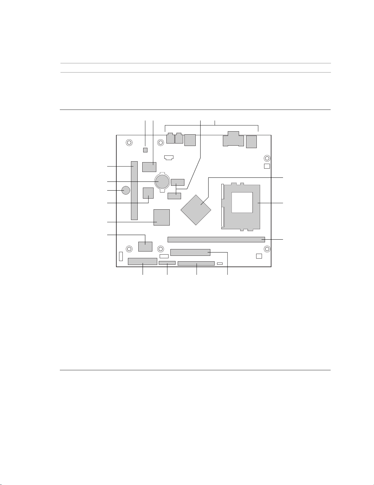
Figure 1 shows the location of the major components on the board.
Q
Product Description
DA B C
P
E
O
N
F
M
L
G
K J I H
OM08923
A Crystal Semiconductor CS4297A codec J Front panel connector
B Creative ES1373D digital audio controller K Power connector
C 4 MB display cache L SMSC LPC47M102 I/O controller
D Back panel I/O connectors M Intel 82801AA ICH
E Intel 82810E DC-133 GMCH N Intel 82559 PCI LAN Controller
F Processor socket O Speaker
G DIMM socket P Battery
H Primary IDE connector Q PCI bus connector
I Slimline Secondary IDE connector
Figure 1. Board Components
11
Page 12
Intel Desktop Board D810EMO/MO810E Technical Product Specification
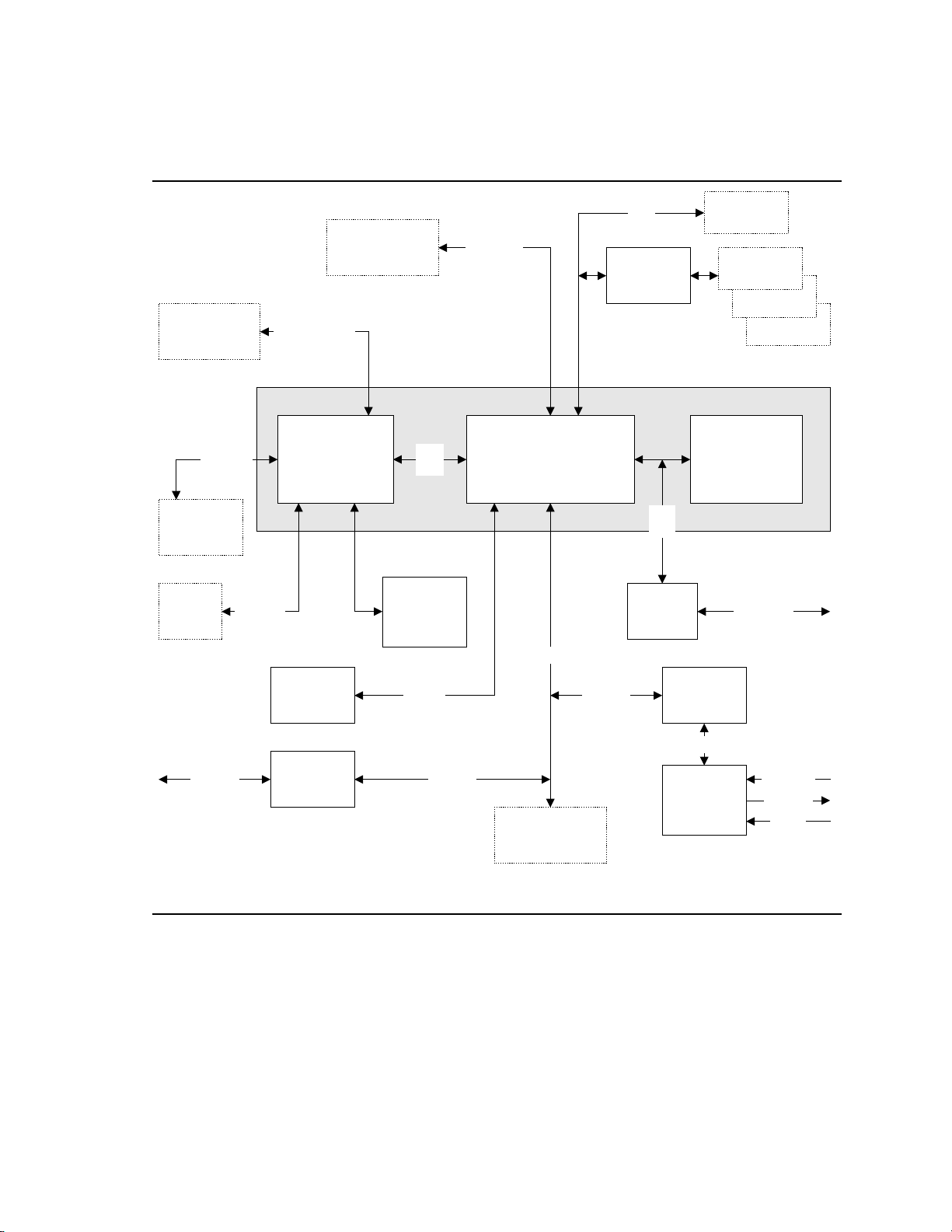
1.1.3 Block Diagram
Figure 2 is a block diagram of the major functional areas of the board.
Primary/
PPGA370
Processor
Socket
Secondary IDE
Interface
66/100/133
MHz Host Bus
810E Chipset
ATA33/66
USB
Hub
Port 0USB
Port 1
Port 2
Port 3
DIMM
Socket
VGA
Port
10/100
Ethernet
100 MHz
SDRAM
Bus
Mbps
Display
Interface
82810E
Graphics Memory
Controller Hub
(GMCH)
Hardware
Monitor
LAN
Subsystem
AHA
Bus
4 MB
Display
Cache
SMBus
PCI Bus
82801AA I/O Controller Hub
(ICH)
PCI Bus
PCI Bus
PCI Bus
Connector
LPC
Bus
LPC I/O
Controller
AC ’97 Link
Firmware Hub
Digital
Controller
Analog
Codec
82802AB
(FWH)
Serial Port
CD-ROM
Line Out
Mic In
12
OM09093
Figure 2. Block Diagram
Page 13

Product Description
1.2 Online Support
Find information about Intel® desktop boards under “Product Info” or “Customer Support” at these
World Wide Web sites:
http://www.intel.com/design/motherbd
http://support.intel.com/support/motherboards/desktop
1.3 Design Specifications
Table 2 lists the specifications applicable to the D810EMO/MO810E board.
Table 2. Specifications
Reference
Name
AC ‘97
ACPI
AGP
AMI BIOS
ATA-3
ATAPI
ATX
El Torito Bootable CD-ROM format
FlexATX FlexATX Addendum to the
Specification
Title
Audio Codec ‘97
Advanced Configuration
and Power Interface
Specification
Accelerated Graphics Port
Interface Specification
American Megatrends
BIOS Specification
Information Technology AT Attachment-3 Interface,
X3T10/2008D
Information Technology
AT Attachment with Packet
Interface Extensions
T13/1153D
ATX Specification
specification
microATX Specification
(2X only)
Version, Revision Date,
and Ownership
Version 2.1,
May 1998,
Intel Corporation.
Version 1.0,
July 1, 1998,
Intel Corporation,
Microsoft Corporation,
and Toshiba Corporation.
Version 2.0,
May 4, 1998,
Intel Corporation.
AMIBIOS 99,
June 1999,
American Megatrends, Inc.
Version 6 ATA Anonymous FTP Site:
Version 18
August 13, 1998,
Contact: T13 Chair,
Seagate Technology
Version 2.01,
February 1997,
Intel Corporation.
Version 1.0,
January 25, 1995,
Phoenix Technologies Ltd.,
and IBM Corporation.
Version 1.0 http://www.teleport.com/~ffsupprt
This specification is
available at:
ftp://download.intel.com/
pc-supp/platform/ac97
http://www.teleport.com/~acpi/
the Accelerated Graphics
Implementers Forum at:
http://www.agpforum.org/
http://www.ami.com/amibios/
bios.platforms.desktop.html
ftp://fission.dt.wdc.com
T13 Anonymous FTP Site:
ftp://fission.dt.wdc.com/
x3t13/project/d1153r18.pdf
http://download.intel.com/
design/motherbd/atx.htm
the Phoenix Technologies web
site at:
http://www.ptltd.com/techs/
specs.html
/spec/FlexATXaddn1_01.pdf
continued
13
Page 14

Intel Desktop Board D810EMO/MO810E Technical Product Specification
Table 2. Specifications (continued)
Reference
Name
†
IrDA
LPC
MicroATX
PCI
Plug and
Play
SDRAM
DIMMs
(64-and
72-bit)
SMBIOS
Specification
Title
Serial Infrared Physical
Layer Link Specification
Low Pin Count Interface
Specification
microATX Motherboard
Interface Specification
SFX Power Supply
Design Guide
PCI Local Bus
Specification
PCI Bus Power
Management Interface
Specification
Plug and Play BIOS
Specification
PC SDRAM Unbuffered
DIMM Specification
PC Serial Presence
Detect (SPD)
Specification
System Management
BIOS
Version, Revision Date, and
Ownership
Version 1.1, October 17, 1995
Infrared Data Association
Phone: (510) 943-6546
Fax: (510) 943-5600
Version 1.0,
September 29, 1997,
Intel Corporation.
Version 1.0,
December 1997
Intel Corporation
Version 1.1,
February 1998
Intel Corporation
Version 2.2,
December 18, 1998,
PCI Special Interest Group.
Version 1.1,
December 18, 1998,
PCI Special Interest Group.
Version 1.0a,
May 5, 1994,
Compaq Computer Corp.,
Phoenix Technologies Ltd.,
and Intel Corporation.
Revision 1.0,
February 1998,
Intel Corporation.
Revision 1.2A,
December 1997,
Intel Corporation
Version 2.3,
August 12, 1998,
Award Software International Inc.,
Dell Computer Corporation,
Hewlett-Packard Company,
Intel Corporation,
International Business Machines
Corporation,
Phoenix Technologies Limited,
American Megatrends Inc.,
and SystemSoft Corporation.
This specification is
available at:
E-mail: irda@netcom.com
http://www.intel.com/
design/chipsets/industry/
lpc.htm
http://www/teleport.com/
~ffsupprt/spec/
microatxspecs.htm
http://www/teleport.com/
~ffsupprt/spec/
microatxspecs.htm
http://www.pcisig.com/
http://www.pcisig.com/
ftp://download.intel.com/
ial/wfm/bio10a.pdf
http://www.intel.com/
design/chipsets/memory/
sdram.htm#S1
http://www.intel.com/
design/chipsets/memory/
sdram.htm#S1
http://developer.intel.com/
ial/wfm/design/smbios
continued
14
Page 15

Table 2. Specifications (continued)
Reference
Name
UHCI
USB
WfM
Specification
Title
Universal Host Controller
Interface Design Guide
Universal Serial Bus
Specification
Wired for Management
Baseline
Version, Revision Date, and
Ownership
Version 1.1,
March 1996,
Intel Corporation.
Version 1.1,
September 23, 1998,
Compaq Computer Corporation,
Intel Corporation, Microsoft
Corporation, and NEC.
Version 2.0,
December 18, 1998,
Intel Corporation
Product Description
This specification is
available at:
This guide is available at:
http://www.usb.org/
developers
http://www.usb.org/
developers/docs.html
http://developer.intel.com/
ial/WfM/wfmspecs.htm
15
Page 16

Intel Desktop Board D810EMO/MO810E Technical Product Specification
1.4 Processor
CAUTION
The board supports processors that draw a maximum of 22 amps. Using a processor that draws
more than 22 amps can damage the processor, the board, and the power supply. See the
processor’s data sheet for current usage requirements.
The board supports the processors listed in Table 3. The host bus frequency is automatically
selected.
Table 3. Processors Supported by the Board
Processor Type Processor Speed Host Bus Frequency L2 Cache Size
600EB MHz 133 MHz 256 KBPentium III processor
600E MHz
550E MHz
500E MHz
Celeron processor 533 MHz
500 MHz
466 MHz
433 MHz
400 MHz
366 MHz
100 MHz
100 MHz
100 MHz
66 MHz
66 MHz
66 MHz
66 MHz
66 MHz
66 MHz
256 KB
256 KB
256 KB
128 KB
128 KB
128 KB
128 KB
128 KB
128 KB
All supported onboard memory can be cached, up to the cachability limit of the processor.
For information about Refer to
Processor support for the D810EMO/MO810E
board
Processor data sheets http://www.intel.com/design/litcentr
http://support.intel.com/support/motherboards/desktop
16
Page 17

Product Description
1.5 System Memory
CAUTION
To be fully compliant with all applicable Intel® SDRAM memory specifications, the board should
be populated with DIMMs that support the Serial Presence Detect (SPD) data structure. If your
memory modules do not support SPD, you will see a notification to this effect on the screen at
power up. The BIOS will attempt to configure the memory controller for normal operation;
however, DIMMs may not function at the determined frequency.
CAUTION
Because the main system memory is also used as video memory, the board requires a 100 MHz
SDRAM DIMM even though the host bus frequency is 66 MHz. It is highly recommended that an
SPD DIMM be used, since this allows the BIOS to read the SPD data and program the chipset to
accurately configure memory settings for optimum performance. If non-SPD memory is installed,
the BIOS will attempt to correctly configure the memory settings, but performance and reliability
may be impacted.
The board has one DIMM socket. The minimum memory size is 32 MB and the maximum
memory size is 256 MB. The BIOS automatically detects memory type, size, and frequency.
The board supports the following memory features:
• 3.3 V, 168-pin DIMM with gold-plated contacts
• 100 MHz SDRAM
• Serial Presence Detect (SPD) or non-SPD memory (BIOS recovery requires an SPD DIMM)
• Non-ECC (64-bit) memory
• Unbuffered single- or double-sided DIMM
The board is designed to support the DIMM configurations listed in Table 4 below.
Table 4. System Memory Configuration
DIMM Size Non-ECC Configuration
32 MB 4 Mbit x 64
64 MB 8 Mbit x 64
128 MB 16 Mbit x 64
256 MB (Note) 32 Mbit x 64
Note: A 256 MB DIMM used with this board must be built with 128 Mbit device technol ogy.
For information about Refer to
The
PC Serial Presence Detect Specification
Obtaining copies of PC SDRAM specifications http://www.intel.com/design/pcisets/memory
Table 2, page 13
17
Page 18
Intel Desktop Board D810EMO/MO810E Technical Product Specification
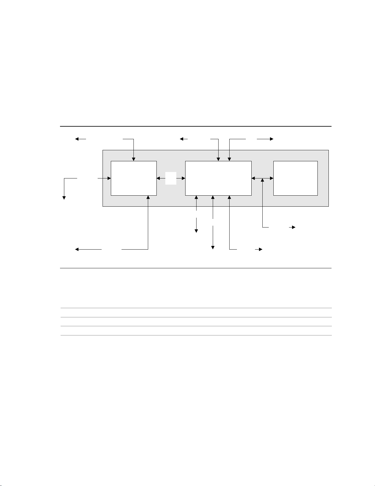
1.6 Intel® 810E Chipset
The Intel 810E chipset consists of the following devices:
• 82810E DC-133 Graphics Memory Controller Hub (GMCH) with accelerated hub architecture
(AHA) bus
• 82801AA I/O Controller Hub (ICH) with AHA bus
• 82802AB Firmware Hub (FWH)
The chipset provides the host, memory, display, and I/O interfaces shown in Figure 3.
66/100/133 MHz
Host Bus
ATA33/66 USB
810E Chipset
100 MHz
SDRAM
Bus
Display
Interface
82810E
Graphics Memory
Controller Hub
(GMCH)
AHA
Bus
82801AA I/O Controller Hub
(ICH)
SMBus
PCI Bus
AC Link
Figure 3. Intel 810E Chipset Block Diagram
For information about Refer to
The Intel 810E chipset http://developer.intel.com
The resources used by the chipset Chapter 2
The chipset’s compliance with ACPI and AC ‘97 Table 2, page 13
82802AB
Firmware Hub
(FWH)
LPC Bus
OM09130
18
Page 19

Product Description
1.6.1 Direct AGP
Direct (integrated) AGP is a high-performance bus (independent of the PCI bus) for
graphics-intensive applications, such as 3-D applications. AGP overcomes certain limitations of
the PCI bus related to handling large amount of graphics data with the following features:
• Pipelined memory read and write operations that hide memory access latency
• Demultiplexing of address and data on the bus for nearly 100 percent bus efficiency
For information about Refer to
The location of the VGA port connector Figure 4, page 39
Obtaining the
Accelerated Graphics Port Interface Specification
Table 2, page 13
1.6.2 USB
The board supports up to four USB ports; one USB peripheral can be connected to each port. For
more than four USB devices, an external hub can be connected to any of the ports. Two USB ports
are implemented with stacked back panel connectors. The other two ports can be routed from the
connector at location J7A1 via a cable to the front panel. The board fully supports UHCI and uses
UHCI-compatible software drivers. USB features include:
• Support for self-identifying peripherals that can be connected or disconnected while the
computer is running
• Automatic mapping of function to driver and configuration
• Support for isochronous and asynchronous transfer types over the same set of wires
• Support for up to 127 physical devices
• Guaranteed bandwidth and low latencies appropriate for telephony, audio, and other
applications
• Error-handling and fault-recovery mechanisms built into the protocol
NOTE
✏
Computer systems that have an unshielded cable attached to a USB port may not meet FCC
Class B requirements, even if no device or a low-speed USB device is attached to the cable. Use
shielded cable that meets the requirements for full-speed devices.
For information about Refer to
The location of the USB connectors on the back panel Figure 4, page 39
The signal names of the USB connectors Table 17, page 40
The location of the USB port connector for the front panel Figure 6, page 46
The signal names for the USB port connector for the front panel Table 30, page 47
The USB and UHCI specifications Table 2, page 13
19
Page 20

Intel Desktop Board D810EMO/MO810E Technical Product Specification
1.6.3 IDE Support
The board has two independent bus-mastering IDE interfaces. These interfaces support:
• ATAPI devices (such as CD-ROM drives)
• ATA devices using the transfer modes listed in Table 51 on page 79
The BIOS supports logical block addressing (LBA) and extended cylinder head sector (ECHS)
translation modes. The drive reports the transfer rate and translation mode to the BIOS.
The board supports laser servo (LS-120) diskette technology through its IDE interfaces. The
LS-120 drive can be configured as a boot device by setting the BIOS Setup program’s Boot menu
to one of the following:
• ARMD-FDD (ATAPI removable media device – floppy disk drive)
• ARMD-HDD (ATAPI removable media device – hard disk drive)
The board has two IDE interface connectors. The primary IDE connector is a standard 40-pin IDE
interface. The secondary IDE connector is a 50-pin Slimline IDE connector, intended for use with
devices such as 2.5-inch hard disk drives and mobile CD-ROM drives. The Slimline IDE
connector has the standard IDE interface pins but also includes audio and power signals.
For information about Refer to
The location of the IDE connectors Figure 5, page 41
The signal names of the primary IDE connector Table 24, page 42
The signal names of the Slimline secondary IDE connector Table 25, page 43
BIOS Setup program’s Boot menu Table 56, page 85
1.6.4 Real-Time Clock, CMOS SRAM, and Battery
The real-time clock is compatible with DS1287 and MC146818 components. The clock provides a
time-of-day clock and a multicentury calendar with alarm features and century rollover. The
real-time clock supports 256 bytes of battery-backed CMOS SRAM in two banks that are reserved
for BIOS use.
A coin-cell battery powers the real-time clock and CMOS memory. When the computer is not
plugged into a wall socket, the battery has an estimated life of three years. When the computer is
plugged in, the 3.3 V standby current from the power supply extends the life of the battery. The
clock is accurate to ± 13 minutes/year at 25 ºC with 3.3 VSB applied.
The time, date, and CMOS values can be specified in the BIOS Setup program. The CMOS values
can be returned to their defaults by using the BIOS Setup program.
NOTE
✏
If the battery and AC power fail, standard defaults, not custom defaults, will be loaded into CMOS
RAM at power on.
20
Page 21

Product Description
NOTE
✏
The recommended method of accessing the date in systems with Intel desktop boards is indirectly
from the Real-Time Clock (RTC) via the BIOS. The BIOS on Intel desktop boards contains a
century checking and maintenance feature. This feature checks the two least significant digits of
the year stored in the RTC during each BIOS request (INT 1Ah) to read the date and, if less than
80 (i.e., 1980 is the first year supported by the PC), updates the century byte to 20. This feature
enables operating systems and applications using the BIOS date/time services to reliably
manipulate the year as a four-digit value.
For information about Refer to
Proper date access in systems with Intel de sktop boards http://support.intel.com/support/year2000/
1.7 I/O Controller
The SMSC LPC47M102 I/O controller provides the following features:
• Low pin count (LPC) interface
• One serial port
• Infrared (IrDA) interface
• Intelligent power management, including a programmable wake up event interface
• Fan control:
One pulse width modulation (PWM) fan speed control output
One fan tachometer input
The BIOS Setup program provides configuration options for the I/O controller.
For information about Refer to
SMSC LPC47M102 I/O controller http://www.smsc.com
The IrDA interface Section 2.8.3, page 46
1.8 Serial Debug Port
The board has one 9-pin serial debug port connector. The serial debug port’s
NS16C550-compatible UART supports data transfers at rates of up to 115.2 kbits/sec with BIOS
support. The serial debug port can be assigned as COM1 (3F8h), COM2 (2F8h), COM3 (3E8h), or
COM4 (2E8h).
For information about Refer to
The location of the serial debug port connector Figure 5, page 41
The signal names of the serial debug port connector Table 26, page 43
21
Page 22

Intel Desktop Board D810EMO/MO810E Technical Product Specification
1.9 Graphics Subsystem
The Intel 82810E DC-133 GMCH graphics memory controller hub component provides the
following graphics support features:
• Integrated 2-D and 3-D graphics engines
• Integrated hardware motion compression engine
• Integrated 230 MHz DAC
Table 5 lists the refresh rates supported by graphics subsystem.
Table 5. Supported Graphics Refresh Rates
Resolution Color Palette Available Refresh Frequencies (Hz)
640 x 480
720 x 480
720 x 576
800 x 600
1024 x 768
1152 x 864
1280 x 1024
1600 x 1200 256 colors 60, 70, 72, 75, 85
16 colors 60, 70, 72, 75, 85
256 colors 60, 70, 72, 75, 85
64 K colors 60, 70, 72, 75, 85
16 M colors 60, 70, 72, 75, 85
256 colors 75, 85
64 K colors 75, 85
16 M colors 75, 85
256 colors 60, 75, 85
64 K colors 60, 75, 85
16 M colors 60, 75, 85
256 colors 60, 70, 72, 75, 85
64 K colors 60, 70, 72, 75, 85
16 M colors 60, 70, 72, 75, 85
256 colors 60, 70, 72, 75, 85
64 K colors 60, 70, 72, 75, 85
16 M colors 60, 70, 72, 75, 85
256 colors 60, 70, 72, 75, 85
64 K colors 60, 70, 72, 75, 85
16 M colors 60, 70, 72, 75, 85
256 colors 60, 70, 72, 75, 85
64 K colors 60, 70, 72, 75, 85
16 M colors 60, 70, 75, 85
22
For information about Refer to
Obtaining graphics software and utilities http://support.intel.com/support/motherboards/desktop
Page 23

Product Description
1.10 Audio Subsystem
The Audio Codec ’97 (AC ’97) compatible audio subsystem includes these features:
• Split digital/analog architecture for improved signal-to-noise ratio (≥ 85 dB) measured at line
out, from any analog input, including line in, and CD-ROM
• 3-D stereo enhancement
• Power management support for ACPI 1.0a
The audio subsystem consists of these devices:
• Creative Sound Blaster AudioPCI 128V
• Crystal Semiconductor CS4297A stereo audio codec
• Audio connectors
For information about Refer to
Obtaining audio software and utilities Section 1.2, page 13
1.10.1 Creative Sound Blaster AudioPCI 128V
The Creative Sound Blaster AudioPCI 128V features:
• Creative ES1373D digital audio controller
• Interfaces to the PCI bus as a Plug and Play device
• 100% DOS legacy compatible
• Access to main memory (through the PCI bus) for wavetable synthesis support – does not
require a separate wavetable ROM device
• Conforms to the PC 98 and PC 99 design guides
For information about Refer to
Creative Sound Blaster AudioPCI 128V http://www.soundblaster.com
1.10.2 Creative ES1373D Digital Audio Controller
The Creative ES1373D digital audio controller’s features include:
• PCI 2.1 compliant
• PCI bus master for PCI audio
• 128-voice wavetable synthesizer
• Aureal A3D
• Ensoniq 3D positional audio and Microsoft DirectSound
†
API, Sound Blaster Pro†, Roland MPU-401 MIDI, joystick compatible
†
3D support
1.10.3 Crystal Semiconductor CS4297A Analog Codec
The Crystal Semiconductor CS4297A is a fully AC ’97 compliant codec. The codec's features
include:
• 18-bit stereo full-duplex operation
• Up to 48 kHz sampling rate
• Connects to ES1373D digital controller using a five-wire digital interface
23
Page 24

Intel Desktop Board D810EMO/MO810E Technical Product Specification
1.10.4 Audio Connectors
The audio connectors include the following:
• Line out (back panel)
• Mic in (back panel)
• ATAPI CD-ROM (connects an internal ATAPI CD-ROM drive to the audio mixer)
For information about Refer to
The back panel audio connectors Section 2.8.1, page 39
The location of the ATAPI CD-ROM connector Figure 5, page 41
The signal names of the ATAPI CD-ROM connector Table 29, page 45
1.11 Hardware Monitor Component
The hardware monitor component provides low-cost instrumentation capabilities. The features of
the component include:
• Internal ambient temperature sensing
• Remote thermal diode sensing for direct monitoring of processor temperature
• Power supply monitoring (+12, +5, +3.3, +2.5, V
acceptable values
• SMBus interface
• The hardware monitor component enables the board to be compatible with the Wired for
Management (WfM) specification.
CCP) to detect levels above or below
For information about Refer to
The board’s compatibility with the WfM specification Table 2, page 13
24
Page 25

Product Description
1.12 LAN Subsystem
The Intel 82559 Fast Ethernet Wired for Management (WfM) PCI LAN subsystem provides both
10Base-T and 100Base-TX connectivity. Features include:
• 32-bit, 33 MHz direct bus mastering on the PCI bus
• 10Base-T and 100Base-TX capability using a single RJ-45 connector with connection and
activity status LEDs
• IEEE 802.3u Auto-Negotiation for the fastest available connection
• Jumperless configuration; the LAN subsystem is completely software-configurable
For information about Refer to
The WfM specification Table 2, page 13
1.12.1 Intel® 82559 PCI LAN Controller
The Intel 82559 PCI LAN controller’s features include:
• CSMA/CD Protocol Engine
• PCI bus interface
• DMA engine for movement of commands, status, and network data across the PCI bus
• Integrated physical layer interface, including:
Complete functionality necessary for the 10Base-T and 100Base-TX network interfaces;
when in 10 Mbit/sec mode, the interface drives the cable directly
A complete set of Media Independent Interface (MII) management registers for control
and status reporting
IEEE 802.3u Auto-Negotiation for automatically establishing the best operating mode
when connected to other 10Base-T or 100Base-TX devices, whether half- or full-duplex
capable
• Integrated power management features, including support for wake on network event (from an ACPI
S3 state using the PCI bus PME# signal)
For information about Refer to
The LAN subsystem’s PCI specification compliance Table 2, page 13
25
Page 26

Intel Desktop Board D810EMO/MO810E Technical Product Specification
1.12.2 LAN Subsystem Software
The Intel 82559 Fast Ethernet WfM PCI LAN software and drivers are available from Intel’s
World Wide Web site.
For information about Refer to
Obtaining LAN software and drivers Section 1.2, page 13
1.12.3 RJ-45 LAN Connector LEDs
Two LEDs are built into the RJ-45 LAN connector. Table 6 describes the LED states when the
board is powered up and the LAN subsystem is operating.
Table 6. LAN Connector LED States
LED Color LED State Condition
Off 10 Mbit/sec data rate is selected.Green
On 100 Mbit/sec date rate is selected.
Yellow
Off LAN link is not established.
On (steady state) LAN link is established.
On (brighter and pulsing) The computer is communicating with another computer on
the LAN.
26
Page 27

Product Description
1.13 Power Management Features
Power management is implemented at several levels, including:
• Advanced Configuration and Power Interface (ACPI)
• Hardware support:
Power connector
Wake on network event
Instantly Available technology
Wake on Ring
Resume on Ring
1.13.1 ACPI
If the board is used with an ACPI-aware operating system, the BIOS can provide ACPI support.
ACPI gives the operating system direct control over the power management and Plug and Play
functions of a computer. The use of ACPI with this board requires the support of an operating
system that provides full ACPI functionality. ACPI features include:
• Plug and Play (including bus and device enumeration)
• Power management control of individual devices, add-in boards (some add-in boards may
require an ACPI-aware driver), video displays, and hard disk drives
• Methods for achieving less than 30-watt system operation in the Power On Suspend sleeping
state, and less than 5-watt system operation in the Suspend to RAM sleeping state
• A Soft-off feature that enables the operating system to power off the computer
• Support for multiple wake up events (see Table 9 on page 29)
• Support for a front panel power and sleep mode switch. Table 7 lists the system states based
on how long the power switch is pressed, depending on how ACPI is configured with an
ACPI-aware operating system.
Table 7. Effects of Pressing the Power Switch
…and the power switch is
If the system is in this state…
Off (ACPI G2/S5 state) Less than four seconds Power on
On (ACPI G0 state) Less than four seconds Soft off/Suspend
On (ACPI G0 state) More than four seconds Fail safe power off
Sleep (ACPI G1 state) Less than four seconds Wake up
Sleep (ACPI G1 state) More than four seconds Power off
For information about Refer to
The board’s compliance level with ACPI Section 1.3, page 13
pressed for …the system enters this state
27
Page 28

Intel Desktop Board D810EMO/MO810E Technical Product Specification
1.13.1.1 System States and Power States
Under ACPI, the operating system directs all system and device power state transitions. The
operating system puts devices in and out of low-power states based on user preferences and
knowledge of how devices are being used by applications. Devices that are not being used can be
turned off. The operating system uses information from applications and user settings to put the
system as a whole into a low-power state.
Table 8 lists the power states supported by the board along with the associated system power
targets. See the ACPI specification for a complete description of the various system and power
states.
Table 8. Power States and Targeted System Power
Global States Sleeping States CPU States Device States Targeted System Power*
G0 – working
state
G1 – sleeping
state
G1 – sleeping
state
G2/S5 S5 – Soft off.
G3 –
mechanical off.
AC power is
disconnected
from the
computer.
* Total system power is dependent on the system configuration, including add-in boards and peripherals powered by the
system chassis’ power supply.
** Dependent on the standby power consumpt i on of wake up devices used in the system.
S0 – working C0 – working D0 – working
state
S1 – CPU stopped C1 – stop
grant
S3 – Suspend-toRAM. Context
saved to RAM.
Context not saved.
Cold boot is
required.
No power to the
system.
No power D3 – no power
No power D3 – no power
No power D3 – no power for
D1, D2, D3 –
device
specification
specific.
except for wake
up logic.
except for wake
up logic.
wake up logic,
except when
provided by
battery or external
source.
Full power > 30 W
5 W < power < 30 W
Power < 5 W **
Power < 5 W **
No power to t he system so
that service can be
performed.
28
Page 29

Product Description
1.13.1.2 Wake Up Devices and Events
Table 9 lists the devices or specific events that can wake the computer from specific states.
Table 9. Wake Up Devices and Events
These devices/events can wake up the computer… …from this state
Power switch S1, S3, S5
RTC alarm S1, S3, S5
LAN S1, S3
Modem S1, S3
USB S1, S3
PCI bus PME# S3
1.13.1.3 Plug and Play
In addition to power management, ACPI provides controls and information so that the operating
system can facilitate Plug and Play device enumeration and configuration. ACPI is used only to
enumerate and configure devices that do not have other hardware standards for enumeration and
configuration. PCI devices on a desktop board, for example, are not enumerated by ACPI.
1.13.2 Hardware Support
CAUTION
If Wake on network event and Instantly Available technology features are used, the power supply
must be capable of providing adequate +5 V standby current. Failure to provide adequate standby
current can damage the power supply. The total amount of standby current required depends on
the wake devices supported and manufacturing options. Refer to Section 2.11.3 on page 54 for
additional information.
The board provides several hardware features that support power management, including:
• Power connector
• Wake on network event
• Instantly Available technology
• Wake on Ring
• Resume on Ring
Wake on network event and Instantly Available technology require power from the +5 V standby
line. The sections discussing these features describe the incremental standby power requirements
for each.
Wake on Ring and Resume on Ring enable telephony devices to access the computer when it is in
a power-managed state. The method used depends on the type of telephony device (external or
internal) and the power management mode being used (ACPI).
NOTE
✏
The use of Wake on Ring and Resume on Ring technologies from an ACPI state require the support
of an operating system that provides full ACPI functionality.
29
Page 30

Intel Desktop Board D810EMO/MO810E Technical Product Specification
1.13.2.1 Power Connector
When used with an ATX-compliant power supply that supports remote power on/off, the board can
turn off the system power through software control. To enable soft-off control in software,
advanced power management must be enabled in the BIOS Setup program and in the operating
system. When the system BIOS receives the correct power management command from the
operating system, the BIOS turns off power to the computer.
With soft-off enabled, if power to the computer is interrupted by a power outage or a disconnected
power cord, when power resumes, the computer returns to the power state it was in before power
was interrupted (on or off).
For information about Refer to
The location of the power connector Figure 5, page 41
The signal names of the power connector Table 27, page 44
The ATX specification Section 1.3, page 13
1.13.2.2 Fan Connectors
The board has two fan connectors. The functions of these connectors are described in Table 10.
Table 10. Fan Connector Descriptions
Connector Function
Chassis fan Provides +12 V DC for a system o r chassis fan.
Processor fan Provides +12 V DC for a processor fan or active fan heatsink.
For information about Refer to
The location of the fan connectors Figure 5, page 41
The signal names of the chassis fan connector Table 22, page 42
The signal names of the processor fan connector Table 23, page 42
1.13.2.3 Wake on Network Event
CAUTION
For Wake on network event, the +5 V standby line for the power supply must be capable of
providing adequate +5 V standby current. Failure to provide adequate standby current when
implementing Wake on network event can damage the power supply. Refer to Section 2.11.3 on
page 54 for additional information.
Wake on network event enables remote wakeup of the computer through a network. The LAN
subsystem, whether onboard or as a PCI bus network adapter, monitors network traffic at the
†
Media Independent Interface. Upon detecting a Magic Packet
wakeup signal that powers up the computer. The board supports Wake on network event through
the PCI bus PME# signal.
, the LAN subsystem asserts a
30
Page 31

Product Description
1.13.2.4 Instantly Available Technology
CAUTION
For Instantly Available technology, the +5 V standby line for the power supply must be capable of
providing adequate +5 V standby current. Failure to provide adequate standby current when
using this feature can damage the power supply. Refer to Section 2.11.3 on page 54 for additional
information.
Instantly Available technology enables the board to enter the ACPI S3 (Suspend-to-RAM) sleepstate. While in the S3 sleep-state, the computer will appear to be off (the power supply is off, the
fans are off, and the power LED is amber). When signaled by a wake up device or event, the
system quickly returns to its last known wake state. Table 9 on page 29 lists the devices and
events that can wake the computer from the S3 state.
The board supports the PCI Bus Power Management Interface Specification. For information on
the versions of these specifications, see Section 1.3. Add-in boards that also support these
specifications can participate in power management and can be used to wake the computer.
1.13.2.5 Wake on Ring
NOTE
✏
Wake on Ring requires the use of a modem (external USB or internal PCI) that supports the Wake
on Ring feature.
The operation of Wake on Ring can be summarized as follows:
• Wakes up the computer from the ACPI S5 state
• Requires two calls to access the computer:
First call restores the computer
Second call enables access (when the appropriate software is loaded)
• Detects incoming calls differently for external as opposed to internal modems:
For external USB modems, the USB bus is monitored for the RING_DETECT signal
For internal PCI modems, incoming calls are detected through the PCI bus PME# signal
1.13.2.6 Resume on Ring
The operation of Resume on Ring can be summarized as follows:
• Resumes operation from the ACPI S1 state
• Requires only one call to access the computer
• Detects incoming call similarly for external and internal modems
31
Page 32

Intel Desktop Board D810EMO/MO810E Technical Product Specification
32
Page 33

2 Technical Reference
What This Chapter Contains
2.1 Introduction................................................................................................................33
2.2 Memory Map ............................................................................................................. 33
2.3 I/O Map ..................................................................................................................... 34
2.4 DMA Channels .......................................................................................................... 35
2.5 PCI Configuration Space Map ................................................................................... 36
2.6 Interrupts...................................................................................................................36
2.7 PCI Interrupt Routing Map......................................................................................... 37
2.8 Connectors................................................................................................................ 38
2.9 Jumper Block............................................................................................................. 49
2.10 Mechanical Considerations........................................................................................ 51
2.11 Electrical Considerations........................................................................................... 53
2.12 Thermal Considerations............................................................................................. 55
2.13 Reliability................................................................................................................... 56
2.14 Environmental............................................................................................................ 57
2.15 Regulatory Compliance............................................................................................. 58
2.1 Introduction
Sections 2.2 – 2.6 contain several standalone tables. Table 11 describes the system memory map,
Table 12 shows the I/O map, Table 13 lists the DMA channels, Table 14 defines the PCI
configuration space map, and Table 15 describes the interrupts. The remaining sections in this
chapter are introduced by text found with their respective section headings.
2.2 Memory Map
Table 11. System Memory Map
Address Range (decimal) Address Range (hex) Size Description
1024 K – 262144 K 100000 – FFFFFFF 255 MB Extended memory
960 K – 1024 K F0000 – FFFFF 64 KB Runtime BIOS
896 K – 960 K E0000 – EFFFF 64 KB Reserved
800 K – 896 K C8000 – DFFFF 96 KB Available high DOS memory (open
to PCI bus)
640 K – 800 K A0000 – C7FFF 160 KB Video memory and BIOS
639 K – 640 K 9FC00 – 9FFFF 1 KB Extended BIOS data (movable by
memory manager software)
512 K – 639 K 80000 – 9FBFF 127 KB Extended conventional memory
0 K – 512 K 00000 – 7FFFF 512 K Conventional memory
33
Page 34

Intel Desktop Board D810EMO/MO810E Technical Product Specification
2.3 I/O Map
Table 12. I/O Map
Address (hex) Size Description
0000 – 000F 16 bytes DMA Controller
0020 – 0021 2 bytes Programmable Interrupt Control (PIC)
0040 – 0043 4 bytes System Timer
0060 1 byte Keyboard controller byte – reset IRQ
0061 1 byte System Speaker
0064 1 byte Keyboard controller, CMD/STAT byte
0070 – 0071 2 bytes System CMOS / Real Time Clock
0072 – 0073 2 bytes System CMOS
0080 – 008F 16 bytes DMA Controller
0092 1 byte Fast A20 and PIC
00A0 – 00A1 2 bytes PIC
00C0 – 00DF 32 bytes DMA
00F0 1 byte Numeric data processor
0170 – 0177 8 bytes Secondary IDE channel
01F0 – 01F7 8 bytes Primary IDE channel
02E8 – 02EF
02F8 – 02FF
0376 1 byte Secondary IDE channel command port
0377, bits 6:0 7 bits Secondary IDE channel status port
03B0 – 03BB 12 bytes Intel 82810E – DC133 Graphics/Memory Controller Hub (GMCH)
03C0 – 03DF 32 byte Intel 82810E – Graphics/Memory Controller Hub (GMCH)
03E8 – 03EF 8 bytes COM3
03F6 1 byte Primary IDE channel command port
03F8 – 03FF 8 bytes COM1
04D0 – 04D1 2 bytes Edge/level triggered PIC
0CF8 – 0CFB
3
0CF9
0CFC – 0CFF 4 bytes PCI configuration data register
FFA0 – FFA7 8 bytes Primary bus master IDE registers
FFA8 – FFAF 8 bytes Secondary bus master IDE registers
1
8 bytes COM4/video (8514A)
1
8 bytes COM2
2
4 bytes PCI configuration address register
1 byte Turbo and reset control register
continued
34
Page 35

Table 12. I/O Map (continued)
Address (hex) Size Description
96 contiguous bytes starting on a
128-byte divisible boundary
64 contiguous bytes starting on a
64-byte divisible boundary
32 contiguous bytes starting on a
32-byte divisible boundary
16 contiguous bytes starting on a
16-byte divisible boundary
4096 contiguous bytes starting on
a 4096-byte divisible boundary
32 contiguous bytes starting on a
32-byte divisible boundary
96 contiguous bytes starting on a
128-byte divisible boundary
64 contiguous bytes starting on a
64-byte divisible boundary
Notes:
1. Default, but can be changed to another address range
2. Dword access only
3. Byte access only
ICH (ACPI + TCO)
Onboard resource
ICH (USB)
ICH (SMBus)
Intel 82810EAA PCI Bridge
Intel 82559 LAN Controller
LPC47M102 PME Status
Creative ES1373D Digital Audio Controller
Technical Reference
✏ NOTE
Some additional I/O addresses are not available due to ICH addresses aliasing. For information
about ICH addressing, refer to Intel web site at:
http://developer.intel.com/design/chipsets/datashts/
2.4 DMA Channels
Table 13. DMA Channels
DMA Channel Number Data Width System Resource
0 8- or 16-bits Audio
1 8- or 16-bits Audio
2 8- or 16-bits Open
3 8- or 16-bits Open / Audio
4 Reserved - cascade channel
5 16-bits Open
6 16-bits Open
7 16-bits Open
35
Page 36

Intel Desktop Board D810EMO/MO810E Technical Product Specification
2.5 PCI Configuration Space Map
Table 14. PCI Configuration Space Map
Bus
Number (hex)
00 00 00 Memory controller of Intel 82810E component
00 01 00 Graphics controller of Intel 82810E component
00 1E 00 Link to PCI bridge
00 1F 00 PCI-to-LPC bridge
00 1F 01 IDE controller
00 1F 02 USB controller #1
00 1F 03 SMBus controller
00 1F 04 Reserved
00 1F 05 AC ’97 audio controller
00 1F 06 AC ’97 modem controller
01 01 00 Intel 82559 PCI LAN controller
01 07 00 PCI Audio Accelerator ES1373D
01 09 00 PCI bus connector
Device
Number (hex)
Function
Number (hex) Description
2.6 Interrupts
Table 15. Interrupts
IRQ System Resource
NMI I/O channel check
0 Reserved, interval timer
1 Reserved, keyboard buffer full
2 Reserved, cascade interrupt from slave PIC
3COM2*
4COM1*
5 User available
6 User available
7 Audio / User available *
8 Real-time Clock
9 Reserved for ICH system management bus
10 User available
11 User available
12 User available
13 Reserved, math coprocessor
14 Primary IDE (if present, else user available)
15 Secondary IDE (if present, else user available)
* Default, but can be changed to anot her IRQ
36
Page 37

Technical Reference
2.7 PCI Interrupt Routing Map
This section describes interrupt sharing and how the interrupt signals are connected between the
PCI bus connector and onboard PCI devices. The PCI specification specifies how interrupts can be
shared between devices attached to the PCI bus. In most cases, the small amount of latency added
by interrupt sharing does not affect the operation or throughput of the devices. In some special
cases where maximum performance is needed from a device, a PCI device should not share an
interrupt with other PCI devices. Use the following information to avoid sharing an interrupt with
a PCI add-in card.
PCI devices are categorized as follows to specify their interrupt grouping:
• INTA: By default, all add-in cards that require only one interrupt are in this category. For
almost all cards that require more than one interrupt, the first interrupt on the card is also
classified as INTA.
• INTB: Generally, the second interrupt on add-in cards that require two or more interrupts is
classified as INTB. (This is not an absolute requirement.)
• INTC and INTD: Generally, a third interrupt on add-in cards is classified as INTC and a
fourth interrupt is classified as INTD.
The ICH PCI-to-LPC bridge has four programmable interrupt request (PIRQ) input signals. Any
PCI interrupt source (either onboard or from a PCI add-in card) connects to one of these
PIRQ signals. Because there are only four signals, some PCI interrupt sources are mechanically
tied together on the board and therefore share the same interrupt. Table 16 lists the PIRQ signals
and shows how the signals are connected to the PCI bus connectors and to onboard PCI interrupt
sources.
Table 16. PCI Interrupt Routing Map
ICH PIRQ Signal Name
✏
PCI Interrupt Source
AGP Controller
ICH Audio Controller
ICH USB Controller
Intel 82559 PCI LAN Controller
PCI Bus Connector
NOTE
PIRQA PIRQB PIRQC PIRQD
INTA
INTC
INTC
INTA INTB INTC INTD
The ICH can connect each PIRQ line internally to one of the IRQ signals (3, 4, 5, 6, 7, 10, 11, 14,
and 15). Typically, a device that does not share a PIRQ line will have a unique interrupt.
However, in certain interrupt-constrained situations, it is possible for two or more of the PIRQ
lines to be connected to the same IRQ signal.
INTD
37
Page 38

Intel Desktop Board D810EMO/MO810E Technical Product Specification
2.8 Connectors
CAUTION
Only the back panel I/O connectors of the board have overcurrent protection. The internal board
connectors are not overcurrent protected, and should connect only to devices inside the computer
chassis, such as fans and internal peripherals. Do not use these connectors for powering devices
external to the computer chassis. A fault in the load presented by the external devices could cause
damage to the computer, the interconnecting cable, and the external devices themselves.
This section describes the board’s connectors. The connectors can be divided into the following
groups:
• Back panel I/O connectors (see page 39)
USB (2)
VGA
LAN
Audio line out
Mic in
• Internal I/O connectors (see page 41)
Fans (2)
IDE (2)
Serial debug port
Power
PCI
ATAPI CD-ROM
• External I/O connectors (see page 46)
USB ports
Front panel (Power/Sleep/Message waiting LED, power switch, hard drive activity LED,
reset switch, and infrared port)
38
Page 39
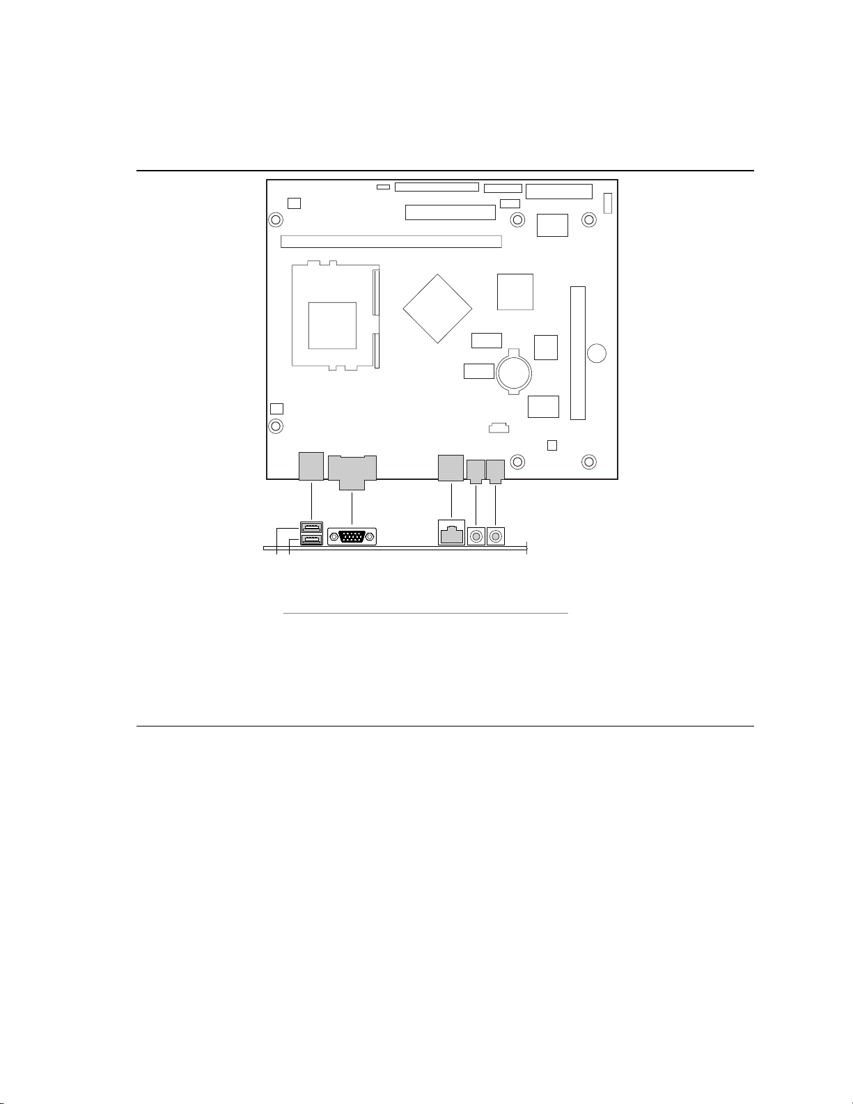
2.8.1 Back Panel I/O Connectors
Figure 4 shows the location of the back panel I/O connectors.
Technical Reference
C DFEAB
OM08925
Item Description
A USB port 0 (see Table 17, page 40)
B USB port 1 (see Table 17, page 40)
C VGA port (see Table 18, page 40)
D LAN (see Table 19, page 40)
E Audio line out (see Table 20, page 40)
F Mic in (see Table 21, page 40)
Figure 4. Back Panel I/O Connectors
NOTE
✏
The back panel audio line out connector is designed to power headphones or amplified speakers
only. Poor audio quality may occur if passive (non-amplified) speakers are connected to this
output.
39
Page 40

Intel Desktop Board D810EMO/MO810E Technical Product Specification
Table 17. USB Connectors
Pin Signal Name
1 +5 V (fused)
2 USBP0# / USBP1#
3 USBP0 / USBP1
4 Ground
Table 18. VGA Port Connector
Pin Signal Name Pin Signal Name Pin Signal Name
1 Red 6 Ground 11 No connect
2 Green 7 Ground 12 MONID1
3 Blue 8 Ground 13 HSYNC
4 No connect 9 Fused VCC 14 VSYNC
5 Ground 10 Ground 15 MONID2
Table 19. LAN Connector
Pin Signal Name
1TX+
2TX3RX+
4 Ground
5 Ground
6RX7 Ground
8 Ground
Table 20. Audio Line Out Connector
Pin Signal Name
Tip Audio left out
Ring Audio right out
Sleeve Ground
Table 21. Mic In Connector
Pin Signal Name
Tip Mono in
Ring Mic bias voltage
Sleeve Ground
40
Page 41

2.8.2 Internal I/O Connectors
Figure 5 shows the location of the internal I/O connectors.
Technical Reference
H
1
G
2
8
2
1
11
1
1
9
10
20
2
1
F E
Item Description Reference Designator
A Fan 2 (chassis fan) (see Table 22, page 42) J2J1
B Fan 1 (processor fan) (see Table 23, page 42) J7J1
C Primary IDE (see Table 24, page 42) J7E1
D Slimline IDE (see Table 25, page 43) J8E1
E Serial debug port (see Table 26, page 43) J7C1
F Power (see Table 27, page 44) J8B1
G PCI (see Table 28, page 45) J4B1
H ATAPI CD-ROM (see Table 29, page 45) J2D1
40
39
50
49
1
CD
1
OM08926
A
B
Figure 5. Internal I/O Connectors
For information about Refer to
The power connector Section 1.13.2.1, page 30
The functions of the fan connectors Section 1.13.2.2, page 30
41
Page 42

Intel Desktop Board D810EMO/MO810E Technical Product Specification
Table 22. Chassis Fan Connector (J2J1)
Pin Signal Name
1 Ground
2 +12 V
3 Ground
Table 23. Processor Fan Connector (J7J1)
Pin Signal Name
1 Ground
2 +12 V
3 FAN_TACH1
Table 24. Primary IDE Connector (J7E1)
Pin Signal Name Pin Signal Name
1 Reset IDE 2 Ground
3 Data 7 4 Data 8
5 Data 6 6 Data 9
7 Data 5 8 Data 10
9 Data 4 10 Data 11
11 Data 3 12 Data 12
13 Data 2 14 Data 13
15 Data 1 16 Data 14
17 Data 0 18 Data 15
19 Ground 20 Key
21 DDRQ0 22 Ground
23 I/O Write# 24 Ground
25 I/O Read# 26 Ground
27 IOCHRDY 28 P_ALE (Cable Sel ect pullup)
29 DDACK0# 30 Ground
31 IRQ 14 32 Reserved
33 DAG1 (Address 1) 34 ATA_66 Detect
35 DAG0 (Address 0) 36 DAG2 (Address 2)
37 Chip Select 1P# 38 Chip Select 3P#
39 Activity# 40 Ground
42
Page 43

Technical Reference
Table 25. Slimline IDE Connector (J8E1)
Pin Signal Name Pin Signal Name
1 AUD_LCR_R 2 AUD_RCD_R
3 AUD_CDGND_R 4 AUD_CDGND_R
5N/C 6N/C
7 Reset IDE 8 Ground
9 Data 7 10 Data 8
11 Data 6 12 Data 9
13 Data 5 14 Data 10
15 Data 4 16 Data 11
17 Data 3 18 Data 12
19 Data 2 20 Data 13
21 Data 1 22 Data 14
23 Data 0 24 Data 15
25 Ground 26 Key
27 DDRQ1 28 Ground
29 I/O Write# 30 Ground
31 I/O Read# 32 Ground
33 IOCHRDY 34 P_ALE (Cable Sel ect pullup)
35 DDACK1# 36 Ground
37 IRQ 15 38 Reserved
39 DAG1 (Address 1) 40 Reserved
41 DAG0 (Address 0) 42 DAG2 (Address 2)
43 Chip Select 1S# 44 Chip Select 3S#
45 Activity# 46 Ground
47 VCC 48 VCC
49 Ground 50 N/C
Table 26. Serial Debug Port Connector (J7C1)
Pin Signal Name Pin Signal Name
1 DCD (Data Carrier Detect) 2 DSR (Data Set Ready)
3 SIN # (Serial Data In) 4 RTS (Request to Send)
5 SOUT # (Serial Data Out) 6 CTS (Clear to Send)
7 DTR (Data Terminal Ready) 8 RI (Ring Indicator)
9 Ground 10 Key
43
Page 44

Intel Desktop Board D810EMO/MO810E Technical Product Specification
Table 27. Power Connector (J8B1)
Pin Signal Name Pin Signal Name
1 +3.3 V 11 +3.3 V
2 +3.3 V 12 -12 V
3 Ground 13 Ground
4 +5 V 14 PS-ON# (power supply remote on/off)
5 Ground 15 Ground
6 +5 V 16 Ground
7 Ground 17 Ground
8 PWRGD (Power Good) 18 PS_FAN_EN
9 +5 VSB 19 +5 V
10 +12 V 20 +5 V
44
Page 45

Technical Reference
Table 28. PCI Bus Connector (J4B1)
Pin Signal Pin Signal Pin Signal Pin Signal
A1 Ground (TRST#)* B1 -12 V A32 AD16 B32 AD17
A2 +12 V B2 Ground (TCK)* A33 +3.3 V B33 C/BE2#
A3 +5 V (TMS)* B3 Ground A34 FRAME# B34 Ground
A4 +5 V (TDI)* B4 No connect (TDO)* A35 Ground B35 IRDY#
A5 +5 V B5 +5 V A36 TRDY# B36 +3.3 V
A6 INTA# B6 +5 V A37 Ground B37 DEVSEL#
A7 INTC# B7 INTB# A38 STOP# B38 Ground
A8 +5 V B8 INTD# A39 +3.3 V B39 LOCK#
A9 Reserved B9 No connect (PRSNT1#)* A40 Reserved B40 PERR#
A10 +5 V (I/O) B10 Reserved A41 Reserved B41 +3.3 V
A11 Reserved B11 No connect (PRSNT2#)* A42 Ground B42 SERR#
A12 Ground B12 Ground A43 PAR B43 +3.3 V
A13 Ground B13 Ground A44 AD15 B44 C/BE1#
A14 +3.3 V aux B14 Reserved A45 +3.3 V B45 AD14
A15 RST# B15 Ground A46 AD13 B46 Ground
A16 +5 V (I/O) B16 CLK A47 AD11 B47 AD12
A17 GNT# B17 Ground A48 Ground B48 AD10
A18 Ground B18 REQ# A49 AD09 B49 Ground
A19 PME# B19 +5 V (I/O) A50 Key B50 Key
A20 AD30 B20 AD31 A51 Key B51 Key
A21 +3.3 V B21 AD29 A52 C/BE0# B52 AD08
A22 AD28 B22 Ground A53 +3.3 V B53 AD07
A23 AD26 B23 AD27 A54 AD06 B54 +3.3 V
A24 Ground B24 AD25 A55 AD04 B55 AD05
A25 AD24 B25 +3.3 V A56 Ground B56 AD03
A26 IDSEL B26 C/BE3# A57 AD02 B57 Ground
A27 +3.3 V B27 AD23 A58 AD00 B58 AD01
A28 AD22 B28 Ground A59 +5 V (I/O) B59 +5 V (I/O)
A29 AD20 B29 AD21 A60 REQ64C# B60 ACK64C#
A30 Ground B30 AD19 A61 +5 V B61 +5 V
A31 AD18 B31 +3.3 V A62 +5 V B62 +5 V
* These signals (in parent hes es) are optional in the PCI spec i fication and are not currently implemented.
Table 29. ATAPI CD-ROM Connector (J2D1)
Pin Signal Name
1 Left audio input from CD-ROM
2 CD audio differential ground
3 CD audio differential ground
4 Right audio input from CD-ROM
45
Page 46

Intel Desktop Board D810EMO/MO810E Technical Product Specification
2.8.3 External I/O Connectors
Figure 6 shows the locations of the external I/O connectors.
2
1
7
10
2
1
16
15
A B
Reference
Item Description
Designator
A USB ports (see Table 30, page 47) J7A1
B Front panel (see Table 31, page 47) J8C1
Figure 6. External I/O Connectors
OM08927
46
Page 47

2.8.3.1 USB Port Connector
Table 30 lists the signal names of the USB port connector.
Table 30. USB Port Connector (J7A1)
Pin Signal Name Pin Signal Name
1 USB_PWR 2 USB_PWR
3 USB_P2RL# 4 USB_P3RL#
5 USB_P2RL 6 USB_P3RL
7 Ground 8 Ground
9 Key (no pin) 10 USB_FP_OC
2.8.3.2 Front Panel Connector
Table 31 lists the signal names of the front panel connector.
Table 31. Front Panel Connector (J8C1)
Pin Signal In/Out Description Pin Signal In/Out Description
Hard Drive Activity LED Power /Sleep / Message Waiting LED
1 HD_PWR Out Hard disk LED pull-up
(330 Ω) to +5 V
3 HD_LED# Out Hard disk active LED 4 HDR_BLNK_YEL Out Front panel
Reset Switch Power Switch
5 GND Ground 6 SW_ON# In Front panel
7 FP_RESET# In Front panel Reset
button
Infrared Port Miscellaneous
9 +5 V Out IR Power 10 N/C In Not connected
11 IRRX In IrDA serial input 12 GND Ground
13 GND Ground 14 (Pin removed) Not connected
15 IRTX Out IrDA serial output 16 +5 V Out Power
Technical Reference
2 HDR_BLNK_GRN Out Front panel
green LED
yellow LED
power switch
8 GND Ground
47
Page 48

Intel Desktop Board D810EMO/MO810E Technical Product Specification
2.8.3.2.1 Power / Sleep / Message Waiting LED Connector
Pins 2 and 4 can be connected to a single- or dual-colored LED. Table 32 lists the possible states
for a single-colored LED. Table 33 shows the possible states for a dual-colored LED.
Table 32. States for a Single-colored Power LED
LED State
Off Not running S1, S3, S5
Steady Green Running S0
Blinking Green Running/message waiting S0
Table 33. States for a Dual-colored Power LED
LED State Description ACPI State
Off Power off S5
Steady Green Running S0
Blinking Green Running/message waiting S0
Steady Yellow Sleeping S1, S3
Blinking Yellow Sleeping/message waiting S1, S3
Description ACPI State
✏ NOTE
To use the message waiting function, ACPI must be enabled in the operating system and a
message-capturing application must be invoked.
2.8.3.2.2 Power Switch Connector
Pins 6 and 8 can be connected to a front panel power switch. The switch must pull pin 6 to ground
for at least 50 ms to signal the power supply to switch on or off. (The time requirement is due to
internal debounce circuitry on the board.) At least two seconds must pass before the power supply
will recognize another on/off signal.
2.8.3.2.3 Hard Drive Activity LED Connector
Pins 1 and 3 can be connected to an LED to provide a visual indicator that data is being read from
or written to a hard drive. For the LED to function properly, an IDE drive must be connected to
the onboard IDE interface.
2.8.3.2.4 Reset Switch Connector
Pins 5 and 7 can be connected to a momentary SPST type switch that is normally open. When the
switch is closed, the board resets and runs the POST.
48
Page 49

Technical Reference
2.9 Jumper Block
CAUTION
Do not move jumpers with the power on. Always turn off the power and unplug the power cord
from the computer before changing a jumper setting. Otherwise, damage to the board could occur.
Figure 7 shows the location of the BIOS Setup jumper block. This 3-pin jumper block determines
the BIOS Setup program’s mode. Table 34 describes the jumper settings for the three modes:
normal, configure, and recovery.
31
J8F1
Figure 7. Location of the Jumper Block
OM08928
49
Page 50

Intel Desktop Board D810EMO/MO810E Technical Product Specification
Table 34. BIOS Setup Configuration Jumper Settings (J8F1)
Function/Mode Jumper Setting Configuration
Normal
1-2
3
The BIOS uses current configuration information and passwords
1
for booting.
Configure
Recovery
2-3
None
3
3
After the POST runs, Setup runs automatically. The maintenance
1
menu is displayed.
The BIOS attempts to recover the BIOS configuration. Bootable
1
recovery media is required.
For information about Refer to
How to access the BIOS Setup program Section 4.1, page 71
The maintenance menu of the BIOS Setup program Section 4.2, page 72
BIOS recovery Section 3.6, page 66
50
Page 51

Technical Reference
2.10 Mechanical Considerations
2.10.1 FlexATX Form Factor
The board is designed to fit into a FlexATX form-factor chassis. The board can also be installed in
a microATX-form-factor chassis. Figure 8 illustrates the mechanical form factor for the board.
Dimensions are given in inches [millimeters]. The outer dimensions are 9.0 inches by 7.5 inches
(228.6 millimeters by 190.5 millimeters). Location of the I/O connectors and mounting holes are
in compliance with the FlexATX addendum of the microATX specification (see Section 1.3).
6.50[165.10]
6.10[154.94]
5.20[132.08]
1.00[25.40]
0.75[19.05]
0.00
1.80[45.72]
0.00
Figure 8. Board Dimensions
8.25[209.55]
8.00[203.20]
OM08929
51
Page 52

Intel Desktop Board D810EMO/MO810E Technical Product Specification
2.10.2 I/O Shield
The back panel I/O shield for the board must meet specific dimension and material requirements.
Systems based on this board need the back panel I/O shield to pass certification testing. Figure 9
shows the critical dimensions of the I/O shield. Dimensions are given in inches [millimeters]. For
dimensions given to two decimal places, the tolerance is ±0.02 inches (±5.08 millimeters). The
figure indicates the position of each cutout. Additional design considerations for I/O shields
relative to chassis requirements are described in the ATX specification. See Section 1.3 for
information about the ATX specification.
0.00
0.47[12.03]
0.68
[17.32]
0.00
0.80
[20.57]
1.64
[41.89]
4.37
[111.14]
5.32
[135.15]
5.82
[147.90]
0.33 Dia(2)
[8.50]
0.46[11.80]
0.66[16.86]
OM08930
52
Figure 9. I/O Shield Dimensions
Page 53

Technical Reference
2.11 Electrical Considerations
2.11.1 Add-in Board Considerations
The board is designed to provide 2 A (average) of +5 V current for an add-in board in the PCI slot.
2.11.2 Power Consumption
Table 35 lists voltage and current specifications for a computer that contains the board and the
following:
• 550E MHz Intel Pentium III processor with a 256 KB cache
• 256 MB SDRAM
• 6.2 GB IDE hard disk drive
• Toshiba Mobile CD-ROM drive
This information is provided only as a guide for calculating approximate power usage with
additional resources added.
Values for the Windows
†
98 desktop mode are measured at 640 x 480 x 256 colors and 60 Hz
refresh rate. AC watts are measured with a typical 145 W power supply, nominal input voltage
and frequency, with true RMS wattmeter at the line input.
Table 35. Power Usage
DC Amps at:
Mode AC Watts +3.3 V +5 V +12 V -12 V +5 VSB
Windows 98 ACPI S0 46 W 1.90 A 2.23 A 0.2 A -0.02 A 0.17 A
Windows 98 ACPI S1 22 W 1.37 A 0.38 A 0.2 A -0.02 A 0.143 A
Windows 98 ACPI S3 1 W 0.0 A 0.0 A 0.0 A 0.0 A 0.13 A
Windows 98 ACPI S5 1 W 0.0 A 0.0 A 0.0 A 0.0 A 0.11 A
53
Page 54

Intel Desktop Board D810EMO/MO810E Technical Product Specification
2.11.3 Power Supply Considerations
System integrators should refer to the power usage values listed in Table 35 when selecting a
power supply for use with this board. The power supply must comply with the following
recommendations found in the indicated sections of the ATX form factor specification
(see Table 2 on page 13).
• The potential relation between +3.3 VDC and +5 VDC power rails (Section 4.2)
• The current capability of the +5 VSB line (Section 4.2.1.2)
• All timing parameters (Section 4.2.1.3)
• All voltage tolerances (Section 4.2.2)
2.11.4 Fan Power Requirements
Table 36 lists the maximum DC voltage and current requirements for the chassis fan when the
board is in sleep mode or normal operating mode. Power consumption is independent of the
operating system used and other variables.
Table 36. Chassis Fan (J3A2) DC Power Requirements
Mode Voltage Maximum Current (Amps)
Normal (S0) + 12 VDC 250 mA
Sleep (S1) + 12 VDC 250 mA
Sleep (S3) + 0 VDC 0 mA
For information about Refer to
The location of the chassis fan connector Figure 5, page 41
The signal names of the chassis fan connector Table 23, page 42
54
Page 55

Technical Reference
2.12 Thermal Considerations
CAUTION
An ambient temperature that exceeds the board’s maximum operating temperature by 5 oC to 10 oC
could cause components to exceed their maximum case temperature and malfunction. For
information about the maximum operating temperature, see the environmental specifications in
Section 2.14.
Figure 10 shows the localized high-temperature zones.
C D EA B
A Creative ES1373D
B Intel 82801AA ICH
C Intel 82810E DC-133 GMCH
D Processor
E Processor voltage regulator area
Figure 10. High Temperature Zones
OM08931
55
Page 56

Intel Desktop Board D810EMO/MO810E Technical Product Specification
Table 37 provides maximum component case temperatures for board components that could be
sensitive to thermal changes. Case temperatures could be affected by the operating temperature,
current load, or operating frequency. Maximum case temperatures are important when considering
proper airflow to cool the board.
Table 37. Thermal Considerations for Components
Component Maximum Case Temperature
Intel Celeron Processor
366 MHz 85 °C
400 MHz 85 °C
433 MHz 85 °C
466 MHz 70 °C
500 MHz 70 °C
533 MHz 70 °C
Intel Pentium III Processor
500E MHz 85 °C
550E MHz 85 °C
600E MHz 85 °C
600EB MHz 85 °C
Intel 82810E DC-133 GMCH 70 °C
Intel 82801AA ICH 100 °C
Creative ES1373D 70 °C
CAUTION
The voltage regulator area can reach a temperature of up to 85 oC in an open chassis. Ensure that
there is proper airflow to this area of the board. Failure to do so may result in damage to the
voltage regulator circuit. System integrators should ensure that proper airflow is maintained in
the voltage regulator circuit (item E in Figure 10). Components in this area could be damaged
without adequate airflow.
2.13 Reliability
The mean time between failures (MTBF) prediction is calculated using component and
subassembly random failure rates. The calculation is based on the Bellcore Reliability Prediction
Procedure, TR-NWT-000332, Issue 4, September 1991. The MTBF prediction is used to estimate
repair rates and spare parts requirements.
The Mean Time Between Failures (MTBF) data is calculated from predicted data at 55 ºC.
Board MTBF: 330,526 hours
56
Page 57

2.14 Environmental
Table 38 lists the environmental specifications for the board.
Table 38. Board Environmental Specifications
Parameter Specification
Temperature
Non-Operating -40 °C to +70 °C
Operating 0 °C to +55 °C
Shock
Unpackaged 30 g trapezoidal waveform
Velocity change of 170 inches/second
Packaged Half sine 2 millisecond
Product Weight (pounds) Free Fall (inches) Velocity Change (inches/sec)
<20 36 167
21-40 30 152
41-80 24 136
81-100 18 118
Vibration
Unpackaged 5 Hz to 20 Hz : 0.01 g² Hz sloping up to 0.02 g² Hz
20 Hz to 500 Hz : 0.02 g² Hz (flat)
Packaged 10 Hz to 40 Hz : 0.015 g² Hz (flat)
40 Hz to 500 Hz : 0.015 g² Hz sloping down to 0.00015 g² Hz
Technical Reference
57
Page 58

Intel Desktop Board D810EMO/MO810E Technical Product Specification
2.15 Regulatory Compliance
This section describes the board’s compliance with safety and EMC regulations.
2.15.1 Safety Regulations
Table 39 lists the safety regulations the board complies with when it is correctly installed in a
compatible host system.
Table 39. Safety Regulations
Regulation Title
UL 1950/CSA950, 3rd edition,
Dated 07-28-95
EN 60950, 2nd Edition, 1992 (with
Amendments 1, 2, 3, and 4)
IEC 950, 2nd edition, 1991 (with
Amendments 1, 2, 3, and 4)
EMKO-TSE (74-SEC) 207/94 Summary of Nordic deviations to EN 60950. (Norway, Sweden,
Bi-National Standard for Safety of Information Technology Equipment
including Electrical Business Equipment. (USA and Canada)
The Standard for Safety of Information Technology Equipment including
Electrical Business Equipment. (European Community)
The Standard for Safety of Information Technology Equipment including
Electrical Business Equipment. (International)
Denmark, and Finland)
2.15.2 EMC Regulations
Table 40 lists the EMC regulations the board complies with when it is correctly installed in a
compatible host system.
Table 40. EMC Regulations
Regulation Title
FCC Class B Title 47 of the Code of Federal Regulations, Parts 2 and 15, Subpart B,
pertaining to unintentional radiators. (USA)
CISPR 22, 2nd Edition, 1993
(Class B)
VCCI Class B (ITE) Implementation Regulations for Voluntary Control of Radio Interference
EN55022 (1994) (Class B) Limits and methods of measurement of Radio Interference
EN50082-1 (1992) Generic Immunity Standard; Currently compliance is determined via
ICES-003 (1997) Interference-Causing Equipment Standard, Digital Apparatus, Class B
AS/NZ 3548 Australian Communications Authority (ACA), Standard for
Limits and methods of measurement of Radio Interference
Characteristics of Information Technology Equipment. (International)
by Data Processing Equipment and Electronic Office Machines.
(Japan)
Characteristics of Information Technology Equipment. (Europe)
testing to IEC 801-2, -3, and -4. (Europe)
(Including CRC c.1374). (Canada)
Electromagnetic Compatibility.
58
Page 59

Technical Reference
2.15.3 Certification Markings
This printed circuit assembly has the following product certification markings:
• UL Joint Recognition Mark: Consists of small c followed by a stylized backward UR and
followed by a small US (Component side)
• Manufacturer’s recognition mark: Consists of a unique UL recognized manufacturer’s logo,
along with a flammability rating (94V-0) (Solder side)
• UL File Number for desktop boards: E139761 (Component side)
• PB Part Number: Intel bare circuit board part number (Solder side) 746506-003
• Battery “+ Side Up” marking: located on the component side of the board in close proximity
to the battery holder
• FCC Logo/Declaration: (Solder side)
• ACA (C-Tick) mark: Consists of a unique letter C, with a tick mark; followed by N-232.
Located on the component side of the board and on the shipping container
• CE Mark: (Component side) The CE mark should also be on the shipping container
59
Page 60

Intel Desktop Board D810EMO/MO810E Technical Product Specification
60
Page 61

3 Overview of BIOS Features
What This Chapter Contains
3.1 Introduction................................................................................................................61
3.2 BIOS Flash Memory Organization............................................................................. 62
3.3 Resource Configuration............................................................................................. 62
3.4 System Management BIOS (SMBIOS)...................................................................... 64
3.5 BIOS Upgrades ......................................................................................................... 65
3.6 Recovering BIOS Data.............................................................................................. 66
3.7 Boot Options.............................................................................................................. 67
3.8 USB Legacy Support................................................................................................. 68
3.9 BIOS Security Features............................................................................................. 69
3.1 Introduction
The board uses an Intel/AMI BIOS, which is stored in flash memory and can be upgraded using a
disk-based program. In addition to the BIOS, the flash memory contains the BIOS Setup program,
POST, the PCI auto-configuration utility, and Plug and Play support.
This board supports system BIOS shadowing, allowing the BIOS to execute from 64-bit onboard
write-protected DRAM.
The BIOS displays a message during POST identifying the type of BIOS and a revision code. The
initial production BIOS is identified as MO81010A.86A.
For information about Refer to
The board’s compliance level with Plug and Play Table 2, page 13
61
Page 62

Intel Desktop Board D810EMO/MO810E Technical Product Specification
3.2 BIOS Flash Memory Organization
The Intel 82802AB Firmware Hub (FWH) includes a 4 Mbit (512 KB) symmetrical flash memory
device. Internally, the device is grouped into eight 64-KB blocks that are individually erasable,
lockable, and unlockable. Figure 11 shows the organization of the flash memory.
The last two 8 KB blocks of the fault tolerance area are the parameter blocks. These blocks
contain data such as BIOS updates, vital product data (VPD), logo, System Management BIOS
(SMBIOS) interface, and extended system configuration data (ESCD) information. The backup
block contains a copy of the fault tolerance block.
080000
07FFFF
070000
06FFFF
060000
05FFFF
050000
04FFFF
040000
03FFFF
030000
02FFFF
020000
01FFFF
010000
00FFFF
000000
64 KB Block
64 KB Block
64 KB Block
64 KB Block
64 KB Block
64 KB Block
64 KB Block
64 KB Block
7
6
5
4
3
2
1
0
Boot Block
Main System BIOS
Fault Tolerance
Backup
8 KB - Parameter Block 2
8 KB - Parameter Block 1
48 KB - Reserved
Figure 11. Memory Map of the Flash Memory Device
3.3 Resource Configuration
3.3.1 PCI Autoconfiguration
The BIOS can automatically configure PCI devices. PCI devices may be onboard or add-in cards.
Autoconfiguration lets a user insert or remove PCI cards without having to configure the system.
When a user turns on the system after adding a PCI card, the BIOS automatically configures
interrupts, the I/O space, and other system resources.
PCI devices can share an interrupt. Autoconfiguration information is stored in ESCD format.
For information about Refer to
The board’s compliance level with Plug and Play Table 2, page 13
OM08376
62
Page 63

Overview of BIOS Features
3.3.2 PCI IDE Support
If you select Auto in the BIOS Setup program, the BIOS automatically sets up the two
PCI IDE connectors with independent I/O channel support. The primary IDE interface supports
hard drives up to ATA/66 and recognizes any ATAPI devices, including CD-ROM drives, tape
drives, and Ultra DMA drives. The secondary IDE interface supports to ATA/33. The BIOS
determines the capabilities of each drive and configures them to optimize capacity and
performance. To take advantage of the high capacities typically available today, hard drives are
automatically configured for Logical Block Addressing (LBA) and to PIO Mode 3 or 4, depending
on the capability of the drive. You can override the auto-configuration options by specifying
manual configuration in the BIOS Setup program.
To use ATA-66 features the following items are required:
• An ATA-66 peripheral device
• An ATA-66 compatible cable
• ATA-66 operating system device drivers
For information about Refer to
The supported version of ATAPI Table 2, page 13
NOTE
✏
Do not connect an ATA device as a slave on the same IDE cable as an ATAPI master device. For
example, do not connect an ATA hard drive as a slave to an ATAPI CD-ROM drive.
63
Page 64

Intel Desktop Board D810EMO/MO810E Technical Product Specification
3.4 System Management BIOS (SMBIOS)
SMBIOS is a Desktop Management Interface (DMI) compliant method for managing computers in
a managed network.
The main component of SMBIOS is the management information format (MIF) database, which
contains information about the computing system and its components. Using SMBIOS, a system
administrator can obtain the system types, capabilities, operational status, and installation dates for
system components. The MIF database defines the data and provides the method for accessing this
®
information. The BIOS enables applications such as Intel
SMBIOS. The BIOS stores and reports the following SMBIOS information:
• BIOS data, such as the BIOS revision level
• Fixed-system data, such as peripherals, serial numbers, and asset tags
• Resource data, such as memory size, cache size, and processor speed
• Dynamic data, such as event detection and error logging
Non-Plug and Play operating systems, such as Windows NT
obtaining the SMBIOS information. The BIOS supports an SMBIOS table interface for such
operating systems. Using this support, an SMBIOS service-level application running on a nonPlug and Play operating system can obtain the SMBIOS information.
LANDesk® Client Manager to use
†
, require an additional interface for
For information about Refer to
The board’s compliance level with SMBIOS Section 1.3, page 13
64
Page 65

Overview of BIOS Features
3.5 BIOS Upgrades
The BIOS can be upgraded using the Intel® Flash Memory Update utility that is available from
Intel. This utility supports the following BIOS maintenance functions:
• Upgrading the flash BIOS from bootable recovery media
• Changing the language section of the BIOS
• Verifying that the upgrade BIOS matches the target system to prevent accidentally installing
an incompatible BIOS
• Updating the BIOS boot block
BIOS upgrades and the Intel Flash Memory Update utility are available from Intel through the
Intel World Wide Web site.
NOTE
✏
Please review the instructions distributed with the upgrade utility before attempting a BIOS
upgrade.
For information about Refer to
The Intel World Wide Web site Section 1.2, page 13
3.5.1 Language Support
The BIOS Setup program and help messages are supported in five languages: US English,
German, Italian, French, and Spanish. The default language is US English, which is present unless
another language is selected in the BIOS Setup program.
3.5.2 Custom Splash Screen
During POST, an Intel splash screen is displayed by default. This splash screen can be replaced
with a custom splash screen. A utility is available from Intel to assist with creating a custom
splash screen. The custom splash screen can be programmed into the flash memory using the
BIOS upgrade utility. Information about this capability is available on the Intel Support World
Wide Web site.
For information about Refer to
The Intel World Wide Web site Section 1.2, page 13
65
Page 66

Intel Desktop Board D810EMO/MO810E Technical Product Specification
3.6 Recovering BIOS Data
Some types of failure can destroy the BIOS. For example, the data can be lost if a power outage
occurs while the BIOS is being upgraded in flash memory. The BIOS can be recovered from
either a 1.44 MB diskette (for recovery from an LS-120 diskette drive configured as an ATAPI
removable IDE device) or from a CD-ROM (for use in an ATAPI CD-ROM drive) using the BIOS
recovery mode. When recovering the BIOS, be aware of the following:
• Recovery requires the use of bootable media in a bootable device.
• Because of the small amount of code available in the nonerasable boot block area, there is no
video support. You can only monitor this procedure by listening to the speaker or looking at
the recovery drive LED.
• Two beeps indicate the beginning of the BIOS recovery process.
• Two beeps and the end of activity in the recovery drive indicate successful BIOS recovery.
• A series of continuous beeps indicates a failed BIOS recovery.
BIOS recovery media can be either a 1.44 MB diskette or a CD-ROM. The recovery media must
be bootable and it must contain the BIOS update files copied to it. BIOS upgrades and the Intel
Flash Memory Upgrade utility are available from Intel Customer Support through the Intel World
Wide Web site.
NOTE
✏
BIOS recovery cannot be accomplished using non-SPD DIMMs. SPD data structure is required
for the recovery process.
NOTE
✏
If the computer is configured to boot from an LS-120 diskette (in the Boot menu), the BIOS
recovery diskette must be a standard 1.44 MB diskette not a 120 MB diskette.
For information about Refer to
The BIOS recovery mode Section 2.9, page 49
The Boot menu in the BIOS Setup program Section 4.7, page 85
Contacting Intel customer support Section 1.2, page 13
66
Page 67

Overview of BIOS Features
3.7 Boot Options
In the BIOS Setup program, the user can choose to boot from an ATAPI removable media device,
hard drives, CD-ROM, or the network. Boot devices are defined in priority order. The default
setting is for the CD-ROM drive to be the primary boot device and the hard drive to be the
secondary boot device.
3.7.1 CD-ROM and Network Boot
Booting from CD-ROM is supported in compliance to the El Torito bootable CD-ROM format
specification. The network can also be selected as a boot device. This selection allows booting
from a network add-in card with a remote boot ROM installed.
For information about Refer to
The El Torito specification Section 1.3, page 13
3.7.2 Booting Without Attached Devices
For use in embedded applications, the BIOS has been designed so that after passing the POST, the
operating system loader is invoked even if the keyboard and mouse are not connected.
67
Page 68

Intel Desktop Board D810EMO/MO810E Technical Product Specification
3.8 USB Legacy Support
USB legacy support enables USB devices such as keyboards, mice, and hubs to be used even when
no operating system USB drivers are in place. By default, USB legacy support is set to Auto.
USB legacy support is used in accessing the BIOS Setup program and installing an operating
system that supports USB.
This sequence describes how USB legacy support operates in the default (auto) mode.
1. When you power up the computer, USB legacy support is disabled.
2. POST begins.
3. USB legacy support is temporarily enabled by the BIOS. This allows you to use a
USB keyboard to enter the BIOS Setup program or the maintenance mode.
4. POST completes and disables USB legacy support (unless it was set to Enabled while in the
BIOS Setup program. Or if set to Auto while in the BIOS Setup program and a USB keyboard
or mouse is connected, then USB Legacy support will be enabled).
5. The operating system loads. While the operating system is loading, USB keyboards and mice
are not recognized (unless USB legacy support was set to Enabled while in the BIOS Setup
program, or if USB legacy support was set to Auto while in the BIOS Setup program and a
USB keyboard or mouse is connected). After the operating system loads the USB drivers, the
USB devices are recognized by the operating system.
To install an operating system that supports USB, enable USB Legacy support or set it to Auto in
the BIOS Setup program and follow the operating system’s installation instructions. Once the
operating system is installed and the USB drivers have been configured, USB legacy support is no
longer used. USB Legacy support can be left enabled or set to auto in the BIOS Setup program if
needed.
Notes on using USB legacy support:
• Do not use USB devices with an operating system that does not support USB. USB legacy is
not intended to support the use of USB devices in a non-USB aware operating system.
• USB legacy support is for keyboards, mice, and hubs only. Other USB devices are not
supported.
68
Page 69

Overview of BIOS Features
3.9 BIOS Security Features
The BIOS includes security features that restrict access to the BIOS Setup program and who can
boot the computer. A supervisor password and a user password can be set for the BIOS Setup
program and for booting the computer, with the following restrictions:
• The supervisor password gives unrestricted access to view and change all the Setup options in
the BIOS Setup program. This is supervisor mode.
• The user password gives restricted access to view and change Setup options in the BIOS Setup
program. This is user mode.
• If only the supervisor password is set, pressing the <Enter> key at the password prompt of the
BIOS Setup program allows the user restricted access to Setup.
• If both the supervisor and user passwords are set, users can enter either the supervisor
password or the user password to access Setup. Users have access to Setup respective to
which password is entered.
• Setting the user password restricts who can boot the computer. The password prompt will be
displayed before the computer is booted. If only the supervisor password is set, the computer
boots without asking for a password. If both passwords are set, the user can enter either
password to boot the computer.
Table 41 shows the effects of setting the supervisor password and user password. This table is for
reference only and is not displayed on the screen.
Table 41. Supervisor and User Password Functions
Supervisor
Password Set
Neither Can change all
Supervisor
only
User only N/A Can change all
Supervisor
and user set
* If no password is set, any user can change all Setup opt i ons .
For information about Refer to
Setting user and supervisor passwords Section 4.4.5, page 82
Mode User Mode Setup Options
options *
Can change all
options
Can change all
options
Can change all
options *
Can change a
limited number
of options
options
Can change a
limited number
of options
None None None
Supervisor Password Supervisor None
Enter Password
Clear User Password
Supervisor Password
Enter Password
Password to
Enter Setup
User User
Supervisor or
user
Password
During Boot
Supervisor or
user
69
Page 70

Intel Desktop Board D810EMO/MO810E Technical Product Specification
70
Page 71

4 BIOS Setup Program
What This Chapter Contains
4.1 Introduction................................................................................................................71
4.2 Maintenance Menu.................................................................................................... 72
4.3 Main Menu................................................................................................................. 74
4.4 Advanced Menu......................................................................................................... 75
4.5 Security Menu............................................................................................................83
4.6 Power Menu.............................................................................................................. 84
4.7 Boot Menu................................................................................................................. 85
4.8 Exit Menu.................................................................................................................. 87
4.1 Introduction
The BIOS Setup program can be used to view and change the BIOS settings for the computer. The
BIOS Setup program is accessed by pressing the <F2> key after the Power-On Self-Test (POST)
memory test begins and before the operating system boot begins. The menu bar is shown below.
Maintenance Main Advanced Security Power Boot Exit
Table 42 lists the BIOS Setup program menu functions.
Table 42. BIOS Setup Program Menu Functions
Maintenance Main Advanced Security Power Boot Exit
Selects boot
options and
power supply
controls
✏
Clears
passwords and
BIS credentials,
enables
extended
configuration
modes
NOTE
Allocates
resources for
hardware
components
Configures
advanced
features
available
through the
chipset
Sets
passwords
and security
features
Configures
power
management
features
The Setup screens described in this chapter apply to boards with BIOS identifier MO81010A.86A.
Boards with other BIOS identifiers might have differences in some of the Setup screens.
NOTE
✏
In this chapter, all examples of the BIOS Setup Program menu bar include the maintenance menu;
however, the maintenance menu is displayed only when the board is in configuration mode.
Section 2.9 on page 49 tells how to put the board in configuration mode.
Saves or
discards
changes to
Setup
program
options
71
Page 72

Intel Desktop Board D810EMO/MO810E Technical Product Specification
Table 43 lists the function keys available for menu screens.
Table 43. BIOS Setup Program Function Keys
BIOS Setup Program Function Key Description
<←> or <→> Selects a different menu screen
<↑> or <↓> Selects an item
<Tab> Selects a field
<Enter> Executes command or selects a submenu
<F9> Load the default configuration values for the current menu
<F10> Save the current values and exits the BIOS Setup program
<Esc> Exits the menu
4.2 Maintenance Menu
To access this menu, select Maintenance on the menu bar at the top of the screen.
Maintenance
Main Advanced Security Power Boot Exit
Extended Configuration
The menu shown in Table 44 is for clearing the Setup passwords and the Wired for Management
Boot Integrity Service credentials, and for changing extended configuration memory settings.
Setup only displays this menu in configuration mode. See Section 2.9 on page 49 for configuration
mode setting information.
Table 44. Maintenance Menu
Feature Options Description
4Clear All Passwords Confirm: Yes/No Selecting
passwords.
4Clear BIS Credentials
(Note)
4Extended Configuration (See Extended
CPU Information:
CPU Microcode Update
Revision
CPU Stepping Signature No options Displays CPU’s Stepping Signature.
Note: For information about the B IS, refer to the Intel web s i te at:
http://developer.i nt el .com/design/sec uri t y/index1.htm
Confirm: Yes/No Selecting
Service) credentials.
Selecting
Configuration Submenu)
No options Displays CPU’s Microcode Update Revision.
control and video memory cache modes.
Yes
clears the user and supervisor
Yes
clears the WfM BIS (Boot Integrity
User-Defined
allows setting system
72
Page 73

4.2.1 Extended Configuration Submenu
To access this submenu, select Maintenance on the menu bar,
Extended Configuration.
then
BIOS Setup Program
Maintenance
Main Advanced Security Power Boot Exit
Extended Configuration
The submenu represented by Table 45 is for setting system control and video memory cache mode.
This submenu becomes available when User-Defined is selected under Extended Configuration.
Table 45. Extended Configuration Submenu
Feature Options Description
Extended Configuration
Memory Control:
SDRAM Auto
Configuration
CAS# Latency • 3
SDRAM RAS# to
CAS# delay
SDRAM RAS#
Precharge
• Default
(default)
• User-Defined
• Auto (default)
• User-Defined
• 2
• Auto (default)
• 3
• 2
• Auto (default)
• 3
• 2
• Auto (default)
Selecting user-defined allows you to select
User-Defined
configure the items listed under Memory Control below.
Note: If
in the Advanced Menu as: “Extended Configuration: Used.”
Sets extended memory configuration options to auto or
user-defined.
Selects the number of clock cycles required to address a
column in memory.
Selects the number of clock cycles between addressing a
row and addressing a column.
Selects the length of time required before accessing a new
row.
. Selecting
User-Defined
User-Defined
is selected, the status will be displayed
Default
allows you to
or
73
Page 74

Intel Desktop Board D810EMO/MO810E Technical Product Specification
4.3 Main Menu
To access this menu, select Main on the menu bar at the top of the screen.
Maintenance
Main
Advanced Security Power Boot Exit
Table 46 describes the Main menu. This menu reports processor and memory information and is
for configuring the system date and system time.
Table 46. Main Menu
Feature Options Description
BIOS Version No options Displays the version of the BIOS.
Processor Type No options Displays processor type.
Processor Speed No options Displays processor speed.
System Bus
Frequency
Cache RAM No options Displays the size of second-level cache.
Total Memory No options Displays the total amount of RAM on the board.
Memory Bank 0 No options Displays type of DIMM installed.
Language English Displays the current language.
Processor Serial
Number
System Time Hour, minute, and
System Date Day of the week,
No options Displays the host bus frequency.
• Disabled (default)
• Enabled
second
month, day, and year
When enabled, displays the processor’s serial number.
(Not supported by all processor types and speeds.)
Specifies the current time.
Specifies the current date.
74
Page 75

4.4 Advanced Menu
To access this menu, select Advanced on the menu bar at the top of the screen.
BIOS Setup Program
Maintenance Main
Advanced
Security Power Boot Exit
Boot Configuration
Peripheral Configuration
IDE Configuration
Event Log Configuration
Video Configuration
Table 47 describes the Advanced menu. This menu is used for setting advanced features that are
available through the chipset.
Table 47. Advanced Menu
Feature Options Description
Extended Configuration No options Indicates the setting of the Extended Configuration submenu
(from the Maintenance Menu)
Used
indicates that the Extended Configuration submenu is
being used.
Not Used
Configuration submenu is not being used.
4Boot Configuration No options Configures Plug and Play and the Numlock key, and resets
configuration data. When selected, displays the Boot
Settings Configuration submenu.
4Peripheral Configuration No options Configures peripheral ports and devices. When selected,
displays the Peripheral Configuration submenu.
4IDE Configuration No options Specifies type of connected IDE device.
4Event Log Configuration No options Configures Event Logging. When selected, displays the
Event Log Configuration submenu.
4Video Configuration No options Specifies the primary video adapter.
(the default) indicates that the Extended
75
Page 76

Intel Desktop Board D810EMO/MO810E Technical Product Specification
4.4.1 Boot Configuration Submenu
To access this submenu, select Advanced on the menu bar,
Boot Configuration.
then
Maintenance Main
Advanced
Security Power Boot Exit
Boot Configuration
Peripheral Configuration
IDE Configuration
Event Log Configuration
Video Configuration
The submenu represented by Table 48 is for setting Plug and Play options, resetting configuration
data, and the power-on state of the Numlock key.
Table 48. Boot Configuration Submenu
Feature Options Description
Plug & Play O/S
Reset Config Data
Numlock • Off
• No (default)
• Yes
• No (default)
• Yes
• On (default)
Specifies if a Plug and Play operating system is be ing used.
No
lets the BIOS configure all devices.
Yes
lets the operating system configure Plug and Play
devices. Not required with Plug and Play operating systems.
Clears the BIOS configuration data on the next boot.
Specifies the power on state of the Numlock feature on the
numeric keypad of the keyboard.
76
Page 77

4.4.2 Peripheral Configuration Submenu
To access this submenu, select Advanced on the menu bar,
Peripheral Configuration.
then
BIOS Setup Program
Maintenance Main
Advanced
Security Power Boot Exit
Boot Configuration
Peripheral Configuration
IDE Configuration
Event Log Configuration
Video Configuration
The submenu represented in Table 49 is used for enabling the onboard serial port, audio and LAN
devices, and legacy USB support.
Table 49. Peripheral Configuration Submenu
Feature Options Description
Serial Port A • Disabled
• Enabled
• Auto (default)
Base I/O address
Interrupt • IRQ 3
Audio Device • Disabled
LAN Device • Disabled
Legacy USB Support • Disabled
• 3F8 (default)
• 2F8
• 3E8
• 2E8
• IRQ 4 (default)
• Enabled (default)
• Enabled (default)
• Enabled (default)
Enables or disables the serial port.
Specifies the base I/O address for the serial port. This
option appears only when Serial Port A is set to
Specifies the interrupt assigned to the serial port. This
option appears only when Serial Port A is set to
Enables or disables the onboard audio subsystem.
Enables or disable the onboard LAN controller.
Enables or disables USB legacy support.
(See Section 3.8 on page 68 for more information.)
Enabled.
Enabled.
77
Page 78

Intel Desktop Board D810EMO/MO810E Technical Product Specification
4.4.3 IDE Configuration Submenu
To access this submenu, select Advanced on the menu bar,
IDE Configuration.
then
Maintenance Main
Advanced
Security Power Boot Exit
Boot Configuration
Peripheral Configuration
IDE Configuration
Primary IDE Master
Primary IDE Slave
Secondary IDE Master
Secondary IDE Slave
Diskette Configuration
Event Log Configuration
Video Configuration
The menu represented in Table 50 is used to configure IDE device options.
Table 50. IDE Configuration Submenu
Feature Options Description
IDE Controller • Disabled
• Primary
• Secondary
• Both (default)
Hard Disk Pre-Delay
4Primary IDE Master No options Reports type of connected IDE device. When selected,
4Primary IDE Slave No options Reports type of connected IDE device. When selected,
4Secondary IDE Master No options Reports type of connected IDE device. When selected,
4Secondary IDE Slave No options Reports type of connected IDE device. When selected,
• Disabled (default)
• 3 Seconds
• 6 Seconds
• 9 Seconds
• 12 Seconds
• 15 Seconds
• 21 Seconds
• 30 Seconds
Specifies the integrated IDE controller.
Primary
Secondary
Both
Specifies the hard disk drive pre-delay.
displays the Primary IDE Master submenu.
displays the Primary IDE Slave submenu.
displays the Secondary IDE Master submenu.
displays the Secondary IDE Slave submenu.
enables only the Primary IDE Controller.
enables only the Secondary IDE Controller.
enables both IDE controllers.
78
Page 79

4.4.3.1 Primary/Secondary IDE Master/Slave Submenus
To access these submenus, select Advanced on the menu bar,
IDE Configuration and then the master or slave to be configured.
then
BIOS Setup Program
Maintenance Main
Advanced
Security Power Boot Exit
Boot Configuration
Peripheral Configuration
IDE Configuration
Primary IDE Master
Primary IDE Slave
Secondary IDE Master
Secondary IDE Slave
Diskette Configuration
Event Log Configuration
Video Configuration
There are four IDE submenus: primary master, primary slave, secondary master, and secondary
slave. Table 51 shows the format of the IDE submenus. For brevity, only one example is shown.
Table 51. Primary/Secondary IDE Master/Slave Submenus
Feature Options Description
Type • None
• User
• Auto (default)
• CD-ROM
• ATAPI Removable
• Other ATAPI
• IDE Removable
LBA Mode Control • Disabled
• Enabled (default)
Multi-Sector Transfers • Disabled
• 2 Sectors
• 4 Sectors
• 8 Sectors
• 16 Sectors (default)
Specifies the IDE configuration mode for IDE devices.
User
allows the user to change the other features in this
table.
Auto
automatically sets the other features in this table.
None
or
Auto
Any setting other than
set features.
Enables or disables the LBA mode control.
Specifies number of sectors per block for transfers from
the hard disk drive to memory.
Check the hard disk drive’s specifications for optimum
setting.
enables the user to
continued
79
Page 80

Intel Desktop Board D810EMO/MO810E Technical Product Specification
Table 51. Primary/Secondary IDE Master/Slave Submenus (continued)
Feature Options Description
PIO Mode
Ultra DMA
Use ARMD Drive As • Auto
• Auto (default)
• 0
• 1
• 2
• 3
• 4
• Disabled (default)
• Mode 0
• Mode 1
• Mode 2
• Mode 3
• Mode 4
• Floppy (default)
• Hard Disk
Configures the PIO mode.
Auto sets the PIO mode to the fastest speed supported.
Specifies the Ultra DMA mode for the drive.
Specifies the type of ARMD drive.
This option appears only if an ARMD drive is attached to
an IDE interface.
80
Page 81

BIOS Setup Program
4.4.4 Event Log Configuration
To access this menu, select Advanced on the menu bar, then Event Log Configuration.
Maintenance Main
Advanced
Security Power Boot Exit
Boot Configuration
Peripheral Configuration
IDE Configuration
Event Log Configuration
Video Configuration
The submenu represented by Table 52 is used to configure the event logging features.
Table 52. Event Log Configuration Submenu
Feature Options Description
Event log No options Indicates if there is space available in the event log.
Event log validity No options Indicates if the contents of the event log are valid.
View event log [Enter] Displays the event log.
Clear all event logs
Event Logging • Disabled
Mark events as read [Enter] Marks all events as read.
• No (default)
• Yes
• Enabled (default)
Clears the event log after rebooting.
Enables logging of events.
81
Page 82

Intel Desktop Board D810EMO/MO810E Technical Product Specification
4.4.5 Video Configuration
To access this menu, select Advanced on the menu bar, then Video Configuration.
Maintenance Main
Advanced
Security Power Boot Exit
Boot Configuration
Peripheral Configuration
IDE Configuration
Event Log Configuration
Video Configuration
The submenu represented by Table 52 is used to select the video adapter.
Table 53. Video Configuration Submenu
Feature Options Description
Primary Video Adapter
• AGP (default)
• PCI
Selects the Direct AGP or PCI video controller as the
display device that will be active when the systems
boots.
82
Page 83

4.5 Security Menu
To access this menu, select Security from the menu bar at the top of the screen.
BIOS Setup Program
Maintenance Main Advanced
Security
Power Boot Exit
The menu represented by Table 54 is for setting passwords and security features.
Table 54. Security Menu
Feature Options Description
Supervisor Password Is No options. Reports if there is a supervisor password set.
User Password Is No options. Reports if there is a user password set.
Set Supervisor Password Password can be up to seven
alphanumeric characters.
Set User Password Password can be up to seven
alphanumeric characters.
Clear User Password
(Note 1)
User Access Level
(Note 2)
Unattended Start
(Note 1)
Notes:
1. This feature appears only i f a user password has been set.
2. This feature appears only i f both a user password and a supervis or password have been set.
• Yes (default)
• No
• Limited
• No Access
• View Only
• Full (default)
• Disabled (default)
• Enabled
Specifies the supervisor password.
Specifies the user password.
Clears the user password.
Sets BIOS Setup Utility access rights for user
level.
Enables or disables Wake on network event
capability. The keyboard remains locked until
a password is entered.
83
Page 84

Intel Desktop Board D810EMO/MO810E Technical Product Specification
4.6 Power Menu
To access this menu, select Power from the menu bar at the top of the screen.
Maintenance Main Advanced Security
Power
Boot Exit
The menu represented in Table 55 is for setting the power management features.
Table 55. Power Menu
Feature Options Description
ACPI Suspend State
• S1 State (default)
• S3 State
Specifies the ACPI suspend state
84
Page 85

4.7 Boot Menu
To access this menu, select Boot from the menu bar at the top of the screen.
BIOS Setup Program
Maintenance Main Advanced Security Power
Boot
IDE Drive Configuration
The menu represented in Table 56 is used to set the boot features and the boot sequence.
Table 56. Boot Menu
Feature Options Description
Quiet Boot • Disabled
• Enabled (default)
Quick Boot • Disabled
• Enabled (default)
Scan User Flash
Area
After Power Failure • Stays Off
On PME
• Disabled (default)
• Enabled
• Last State (default)
• Power On
• Stay Off (default)
• Power On
Disabled
Enabled
messages.
Enables the computer to boot without running certain
POST tests.
Enables the BIOS to scan the flash memory for user
binary files that are executed at boot time.
Specifies the mode of operation if an AC/Power loss
occurs.
Power On
Stay Off
pressed.
Last State
power loss occurred.
Specifies how the computer responds to a PME wakeup
event when the power is off (from an ACPI S3 state).
displays normal POST messages.
displays the OEM logo instead of POST
restores power to the computer.
keeps the power off until the power button is
restores the previous power state before
Exit
continued
85
Page 86

Intel Desktop Board D810EMO/MO810E Technical Product Specification
Table 56. Boot Menu (continued)
Feature Options
First Boot Device
Second Boot Device
Third Boot Device
Fourth Boot Device
• ARMD-FDD
(Note 1)
• ARMD-HDD
(Note 2)
• IDE-HDD
• ATAPI CDROM
• Intel UNDI,
PXE 2.0 (Note 3)
• Disabled
st
• 1
4IDE Drive Configuration
Primary Master IDE
Primary Slave IDE
Secondary Master IDE
IDE (default)
nd
• 2
IDE
rd
• 3
IDE
th
• 4
IDE
Secondary Slave IDE
Notes:
1. ARMD-FDD = ATAPI removable device - f l oppy disk drive (LS-120)
2. ARMD-HDD = ATAPI removable device - hard di s k drive
3. UNDI = Univ ersal network interface card (NIC) driver interfac e
PXE = Pre-boot execution environment
Description
Specifies the boot sequence according to the device
type. The computer will attempt to boot from up to
four devices as specified here. Only one of the
devices can be an IDE hard disk drive.
To specify the boot sequence:
1. Select the boot device with <↑> or <↓>.
2. Press <Enter> to set the selection as the intended
boot device.
The default settings for the first through fourth boot
devices are, respectively:
• ATAPI CDROM
• IDE-HDD
• Intel UNDI, PXE 2.0 (build 071)
• Disabled
NOTE: To configure the computer to boot from an
IDE hard disk drive, set a boot device in this Setup
feature to
IDE-HDD
master or slave mode of the drive. Then, in the next
Setup feature,
channel and mode to
1st IDE
specifies the IDE hard disk drive to boot from.
nd
The
2
through
note above for more information.
To specify the drive to boot from:
1. Use <↑> or <↓> to select the channel, and master
or slave mode of the drive to boot from.
2. Press <Enter>.
3. Use <↑> or <↓> to select 1
4. Press <Enter> to set the selection.
. Determine the IDE channel, and
IDE Drive Configuration
1st IDE
.
4th IDE
settings are ignored. See the
st
IDE.
, set that
86
Page 87

4.8 Exit Menu
To access this menu, select Exit from the menu bar at the top of the screen.
BIOS Setup Program
Maintenance Main Advanced Security Power Boot
Exit
The menu represented in Table 57 is for exiting the BIOS Setup program, saving changes, and
loading and saving defaults.
Table 57. Exit Menu
Feature Description
Exit Saving Changes Exits and saves the changes in CMOS SRAM.
Exit Discarding Changes Exits without saving any changes made in the BIOS Setup program.
Load Setup Defaults Loads the factory default values for all the Setup options.
Load Custom Defaults Loads the custom defaults for Setup options.
Save Custom Defaults Saves the current values as custom defaults. Normally, the BIOS reads the
Setup values from flash memory. If this memory is corrupted, the BIOS reads the
custom defaults. If no custom defaults are set, the BIOS reads the factory
defaults.
Discard Changes Discards changes without exiting Setup. The option values present when the
computer was turned on are used.
87
Page 88

Intel Desktop Board D810EMO/MO810E Technical Product Specification
88
Page 89

5 Error Messages and Beep Codes
What This Chapter Contains
5.1 BIOS Error Messages................................................................................................ 89
5.2 Port 80h POST Codes............................................................................................... 91
5.3 Bus Initialization Checkpoints.................................................................................... 95
5.4 Speaker.....................................................................................................................96
5.5 BIOS Beep Codes..................................................................................................... 97
5.1 BIOS Error Messages
Table 58 lists the error messages and provides a brief description of each.
Table 58. BIOS Error Messages
Error Message Explanation
GA20 Error An error occurred with Gate-A20 when switching to protected
mode during the memory test.
Pri Master HDD Error
Pri Slave HDD Error
Sec Master HDD Error
Sec Slave HDD Error
Pri Master Drive - ATAPI Incompatible
Pri Slave Drive - ATAPI Incompatible
Sec Master Drive - ATAPI Incompatible
Sec Slave Drive - ATAPI Incompatible
Cache Memory Bad An error occurred when testing L2 cache. Cache memory may be
CMOS Battery Low The battery may be losing power. Replace the battery soon.
CMOS Display Type Wrong The display type is different than what has been stored in CMOS.
CMOS Checksum Bad The CMOS checksum is incorrect. CMOS memory may have
CMOS Settings Wrong CMOS values are not the same as the last boot. These values
CMOS Date/Time Not Set The time and/or date values stored in CMOS are invalid. Run
DMA Error Error during read/write test of DMA controller.
HDC Failure Error occurred trying to access hard disk controller.
Could not read sector from corresponding drive.
Corresponding drive is not an ATAPI device. Run Setup to make
sure device is selected correctly.
bad.
Check Setup to make sure type is correct.
been corrupted. Run Setup to reset values.
have either been corrupted or the battery has failed.
Setup to set correct values.
continued
89
Page 90

Intel Desktop Board D810EMO/MO810E Technical Product Specification
Table 58. BIOS Error Messages (continued)
Error Message Explanation
Checking NVRAM..... NVRAM is being checked to see if it is valid.
Update OK! NVRAM was invalid and has been updated.
Updated Failed NVRAM was invalid but was unable to be updated.
Keyboard Error Error in the keyboard connection. Make sure keyboard is
connected properly.
Memory Size Decreased Memory size has decreased since the last boot. If no memory
was removed then memory may be bad.
Memory Size Increased Memory size has increased since the last boot. If no memory was
added there may be a problem with the system.
Memory Size Changed Memory size has changed since the last boot. If no memory was
added or removed then memory may be bad.
No Boot Device Available System did not find a device to boot.
Off Board Parity Error A parity error occurred on an offboard card. This error is followed
by an address.
On Board Parity Error A parity error occurred in onboard memory. This error is followed
by an address.
Parity Error A parity error occurred in onboard memory at an unknown
address.
NVRAM / CMOS / PASSWORD cleared
by Jumper
<CTRL_N> Pressed CMOS is ignored and NVRAM is cleared. User must enter Setup.
NVRAM, CMOS, and passwords have been cleared. The system
should be powered down and the jumper removed.
90
Page 91

Error Messages and Beep Codes
5.2 Port 80h POST Codes
During the POST, the BIOS generates diagnostic progress codes (POST-codes) to I/O port 80h. If
the POST fails, execution stops and the last POST code generated is left at port 80h. This code is
useful for determining the point where an error occurred.
Displaying the POST-codes requires an add-in card (often called a POST card). The POST card
can decode the port and display the contents on a medium such as a seven-segment display.
The tables below offer descriptions of the POST codes generated by the BIOS. Table 59 defines
the Uncompressed INIT Code Checkpoints, Table 60 describes the Boot Block Recovery Code
Checkpoints, and Table 61 lists the Runtime Code Uncompressed in F000 Shadow RAM. Some
codes are repeated in the tables because that code applies to more than one operation.
Table 59. Uncompressed INIT Code Checkpoints
Code Description of POST Operation
D0 NMI is disabled. Onboard KBC, RTC enabled (if present). Init code Checksum verification
starting.
D1 Keyboard controller BAT test, CPU ID saved, and going to 4 GB flat mode.
D3 Do necessary chipset initialization, start memory refresh, do memory sizing.
D4 Verify base memory.
D5 Init code to be copied to segment 0 and control to be transferred to segment 0.
D6 Control is in segment 0. To check recovery mode and verify main BIOS checksum. If the B IOS is
in recovery mode or the main BIOS checksum is bad, go to check point E0 for recovery else go to
check point D7 for giving control to main BIOS.
D7 Find main BIOS module in ROM image.
D8 Uncompress the main BIOS module.
D9 Copy main BIOS image to F000 shadow RAM and give control to main BIOS in F000 shadow
RAM.
Table 60. Boot Block Recovery Code Checkpoints
Code Description of POST Operation
E0 Onboard floppy controller (if any) is initialized. Compressed recovery code is uncompressed in
F000:0000 in shadow RAM and give control to recovery code in F000 Shadow RAM. Initialize
interrupt vector tables, initialize system ti mer, initialize DMA cont roller, interrupt co ntroller.
E8 Initialize extra (Intel Recovery) Module.
E9 Initialize floppy drive.
EA Try to boot from floppy. If reading of boot sector is successful, give control to boot sector code.
EB Booting from floppy failed, look for ATAPI (LS-120, Zip†) devices.
EC Try to boot from ATAPI. If reading of boot sector is successful, give control to boot sector code.
EF Booting from floppy and ATAPI device failed. Give two beeps. Retry the booting procedure again
(go to check point E9).
91
Page 92

Intel Desktop Board D810EMO/MO810E Technical Product Specification
Table 61. Runtime Code Uncompressed in F000 Shadow RAM
Code Description of POST Operation
03 NMI is Disabled. To check soft reset/power-on.
05 BIOS stack set. Going to disable cache if any.
06 POST code to be uncompressed.
07 CPU init and CPU data area init to be done.
08 CMOS checksum calculation to be done next.
0B Any initialization before keyboard BAT to be done next.
0C KB controller I/B free. To issue the BAT command to keyboard controller.
0E Any initialization after KB controller BAT to be done next.
0F Keyboard command byte to be written.
10 Going to issue Pin-23, 24 blocking/unblocking command.
11 Going to check pressing of <INS>, <END> key during power-on.
12 To init CMOS if "Init CMOS in every boot" is set or <END> key is pressed. Going to disable DMA
and Interrupt controllers.
13 Video display is disabled and port-B is initialized. Chipset init about to begin.
14 8254 timer test about to start.
19 About to start memory refresh test.
1A Memory Refresh line is toggling. Going to check 15 µs ON/OFF time.
23 To read 8042 input port and disable Megakey GreenPC feature. Make BIOS code segment
writeable.
24 To do any setup before Int vector init.
25 Interrupt vector initialization to begin. To clear password if necessary.
27 Any initialization before setting video mode to be done.
28 Going for monochrome mode and color mode setting.
2A Different buses init (system, static, ou tput devices) to start if present. (See Section 5.3 for details
of different buses.)
2B To give control for any setup required before optional video ROM check.
2C To look for optional video ROM and give control.
2D To give control to do any processing after video ROM returns control.
2E If EGA/VGA not found then do display memory R/W test.
2F EGA/VGA not found. Display memory R/W test about to begin.
30 Display memory R/W test passed. About to look for the retrace checking.
31 Display memory R/W test or retrace checking failed. To do alternate display memory R/W test.
32 Alternate display memory R/W test passed. To look for the alternate display retrace checking.
34 Video display checking over. Display mode to be set next.
37 Display mode set. Going to display the power on message.
38 Different buses init (input, IPL, general devices) to start if present. (See Section 5.3 for details of
different buses.)
39 Display different buses initialization error messages. (See Section 5.3 for details of different
buses.)
3A New cursor position read and saved. To display the Hit <DEL> message.
continued
92
Page 93

Error Messages and Beep Codes
Table 61. Runtime Code Uncompressed in F000 Shadow RAM (continued)
Code Description of POST Operation
40 To prepare the descriptor tables.
42 To enter in virtual mode for memory test.
43 To enable interrupts for diagnostics mode.
44 To initialize data to check memory wrap around at 0:0.
45 Data initialized. Going to check for memory wrap around at 0:0 and finding the total system
memory size.
46 Memory wrap around test done. Memory size calculation over. About to go for writing patterns to
test memory.
47 Pattern to be tested written in extended memory. Going to write patterns in base 640 K memory.
48 Patterns written in base memory. Going to find out amount of memory below 1 M memory.
49 Amount of memory below 1 M found and verified. Going to find out amount of memory above 1 M
memory.
4B Amount of memory above 1 M found and verified. Check for soft reset and going to clear memory
below 1 M for soft reset. (If power on, go to check point # 4Eh).
4C Memory below 1 M cleared. (SOFT RESET) Going to clear memory above 1 M.
4D Memory above 1 M cleared. (SOFT RESET) Going to save the memory size. (Go to check
point # 52h).
4E Memory test started. (NOT SOFT RESET) About to display the first 64 K memory size.
4F Memory size display started. This will be updated during memory test. Going for sequential and
random memory test.
50 Memory testing/initialization below 1 M complete. Going to adjust displayed memory size for
relocation/ shadow.
51 Memory size display adjusted due to relocation/shadow. Memory test above 1 M to follow.
52 Memory testing/initialization above 1 M complete. Going to save memory size information.
53 Memory size information is saved. CPU registers are saved. Going to enter in real mode.
54 Shutdown successful, CPU in real mode. Going to disable gate A20 line and disable parity/NMI.
57 A20 address line, parity/NMI disable successful. Going to adjust memory size depending on
relocation/shadow.
58 Memory size adjusted for relocation/shadow. Going to clear Hit <DEL> message.
59 Hit <DEL> message cleared. <WAIT...> message displayed. About to start DMA and interrupt
controller test.
60 DMA page register test passed. To do DMA#1 base register test.
62 DMA#1 base register test passed. To do DMA#2 base register test.
65 DMA#2 base register test passed. To program DMA unit 1 and 2.
66 DMA unit 1 and 2 programming over. To initialize 8259 interrupt controller.
7F Extended NMI sources enabling is in progress.
80 Keyboard test started. Clearing output buffer, checking for stuck key, to issue keyboard reset
command.
81 Keyboard reset error/stuck key found. To issue keyboard controller interface test command.
82 Keyboard controller interface test over. To write command byte and init circular buffer.
83 Command byte written, global data init done. To check for lock-key.
continued
93
Page 94

Intel Desktop Board D810EMO/MO810E Technical Product Specification
Table 61. Runtime Code Uncompressed in F000 Shadow RAM (continued)
Code Description of POST Operation
84 Lock-key checking over. To check for memory size mismatch with CMOS.
85 Memory size check done. To display soft error and check for password or bypass setup.
86 Password checked. About to do programming before setup.
87 Programming before setup complete. To uncompress SETUP code and execute CMOS setup.
88 Returned from CMOS setup program and screen is cleared. About to do programming after
setup.
89 Programming after setup complete. Going to display power on screen message.
8B First screen message displayed. <WAIT...> message displayed. PS/2 Mouse check and
extended BIOS data area allocation to be done.
8C Setup options programming after CMOS setup about to start.
8D Going for hard disk controller reset.
8F Hard disk controller reset done. Floppy setup to be done next.
91 Floppy setup complete. Hard disk setup to be done next.
95 Init of different buses optional ROMs from C800 to start. (See Section 5.3 for details of different
buses.)
96 Going to do any init before C800 optional ROM control.
97 Any init before C800 optional ROM control is over. Optional ROM check and control will be done
next.
98 Optional ROM control is done. About to give control to do any required processing after optional
ROM returns control and enable external cache.
99 Any initialization required after optional ROM test over. Going to setup timer data area and printer
base address.
9A Return after setting timer and printer base address. Going to set the RS-232 base address.
9B Returned after RS-232 base address. Going to do any initialization before coprocessor test.
9C Required initialization before coprocessor is over. Going to initialize the coprocessor next.
9D Coprocessor initialized. Going to do any initialization after coprocessor test.
9E Initialization after coprocessor test is complete. Going to check extended keyboard, keyboard ID,
and Num Lock.
A2 Going to display any soft errors.
A3 Soft error display complete. Going to set keyboard typematic rate.
A4 Keyboard typematic rate set. To program memory wait states.
A5 Going to enable parity/NMI.
A7 NMI and parity enabled. Going to do any initialization required before giving control to optional
ROM at E000.
A8 Initialization before E000 ROM control over. E000 ROM to get control next.
A9 Returned from E000 ROM control. Going to do any initialization required after E000 optional
ROM control.
AA Initialization after E000 optional ROM control is over. Going to display the system configuration.
AB Put INT13 module runtime image to shadow.
AC Generate MP for multiprocessor support (if present).
AD Put CGA INT10 module (if present) in shadow.
continued
94
Page 95

Error Messages and Beep Codes
Table 61. Runtime Code Uncompressed in F000 Shadow RAM (continued)
Code Description of POST Operation
AE Uncompress SMBIOS module and init SMBIOS code and form the runtime SMBIOS image in
shadow.
B1 Going to copy any code to specific area.
00 Copying of code to specific area done. Going to give control to INT19 boot loader.
5.3 Bus Initialization Checkpoints
The system BIOS gives control to the different buses at several checkpoints to do various tasks.
Table 62 describes the bus initialization checkpoints.
Table 62. Bus Initialization Checkpoints
Checkpoint Description
2A Different buses init (syst em, static, and output devices) to start if present.
38 Different buses init (input, IPL, and general devices) to start if present.
39 Display different buses initialization error messages.
95 Init of different buses optional ROMs from C800 to start.
While control is inside the different bus routines, additional checkpoints are output to port 80h as a
WORD to identify the routines under execution. In these WORD checkpoints, the low byte of the
checkpoint is the system BIOS checkpoint from which the control is passed to the different bus
routines. The high byte of the checkpoint is the indication of which routine is being executed in
the different buses. Table 63 describes the upper nibble of the high byte and indicates the function
that is being executed.
Table 63. Upper Nibble High Byte Functions
Value Description
0 func#0, disable all devices on the bus concerned
1 func#1, static devices init on the bus concerned
2 func#2, output device init on the bus concerned
3 func#3, input device init on the bus concerned
4 func#4, IPL device init on the bus concerned
5 func#5, general device init on the bus concerned
6 func#6, error reporting for the bus concerned
7 func#7, add-on ROM init for all buses
95
Page 96

Intel Desktop Board D810EMO/MO810E Technical Product Specification
Table 64 describes the lower nibble of the high byte and indicates the bus on which the routines are
being executed.
Table 64. Lower Nibble High Byte Functions
Value Description
0 Generic DIM (Device Initialization Manager)
1 Onboard system devices
2 ISA devices
3 EISA devices
4 ISA PnP devices
5 PCI devices
5.4 Speaker
A 47 Ω inductive speaker is mounted on the board. The speaker provides audible error code (beep
code) information during the power-on self-test (POST).
For information about Refer to
The location of the onboard speaker Figure 1, page 11
96
Page 97

Error Messages and Beep Codes
5.5 BIOS Beep Codes
Whenever a recoverable error occurs during power-on self-test (POST), the BIOS displays an error
message describing the problem (see Table 65). The BIOS also issues a beep code (one long tone
followed by two short tones) during POST if the video configuration fails (a faulty video card or
no card installed) or if an external ROM module does not properly checksum to zero.
An external ROM module (for example, a video BIOS) can also issue audible errors, usually
consisting of one long tone followed by a series of short tones. For more information on the beep
codes issued, check the documentation for that external device.
There are several POST routines that issue a POST terminal error and shut down the system if they
fail. Before shutting down the system, the terminal-error handler issues a beep code signifying the
test point error, writes the error to I/O port 80h, attempts to initialize the video and writes the error
in the upper left corner of the screen (using both monochrome and color adapters).
If POST completes normally, the BIOS issues one short beep before passing control to the
operating system.
Table 65. Beep Codes
Beep Description
1 Refresh failure
2 Parity cannot be reset
3 First 64 KB memory failure
4 Timer not operational
5 Not used
6 8042 GateA20 cannot be toggled
7 Exception interrupt error
8 Display memory R/W error
9 Not used
10 CMOS Shutdown register test error
11 Invalid BIOS (e.g. POST module not found, etc.)
97
Page 98

Intel Desktop Board D810EMO/MO810E Technical Product Specification
98
 Loading...