

Page 1

Intel®Desktop Board
D810E2CB
Technical Product Specification
January 2001
Order Number A44673-001
The Intel®Desktop Board D810E2CB may contain design defects or errors knowna serratathat may cause the product to deviate from published specifications. Current characterized
errata are documented in the Intel Desktop Board D810E2CB Specification Update.
Page 2

Revision History
Revision Revision History Date
001 First release of the Intel®Desktop Board D810E2CB Technical Product
Specification.
This product specification applies to only standard D810E2CB boards with BIOS identifier
CB81010A.86A.
®
Changes to this specification will be published in the Intel
Desktop Board D810E2CB Specification
Update before being incorporated into a revision of this documen t.
INFORMATION IN THIS DOCUMENT IS PROVIDED IN CONNECTION WITH INTEL®PRODUCTS. EXCEPT AS
PROVIDED IN INTEL'S TERMS AND CONDITIONS OF SALE FOR SUCH PRODUCTS, INTEL ASSUMES NO LIABILITY
W HATSOEVER, AND INTEL DISCLAIMS ANY EXPRESS OR IMPLIED WARRANTY, RELATING TO SALE AND/OR USE
OF INTEL PRODUCTS INCLUDING LIABILITY OR WARRANTIES RELATING TO FITNESS FOR A PARTICULAR
PURPOSE, MERCHANTABILITY, OR INFRINGEMENT OF ANY PATENT, COPYRIGHT, OR OTHER INTELLECTUAL
PROPERTY RIGHT.
January 2001
Intel Corporation mayhave patents or pending patent applications, trademarks, copyrights, or other intellectual property rights that
relate to the presented subject matter. The furnishing of documents and other materials and information does not provide any
license, express or implied, by estoppel or otherwise, to any such patents, trademarks, copyrights, or other intellectual property
rights.
Intel products are not intended for use in medical, lifesaving, or life sustaining applications or for anyother application in which
the failure of the Intel product could create a situation where personal injury or death may occur.
Intel may make changes to specifications and product descriptions at any time, without notice.
The D810E2CB board may contain design defects or errors known as errata that may causethe product to deviate from
published specifications. Current characterized errata are availableon request.
Contact your local Intel sales office or your distributor to obtain the latest specifications before placing your product order.
Copies of documents which have an ordering number and are referenced in this document, or other Intel literature, may be
obtained from:
Intel Corporation
P.O. Box 5937
Denver,CO 80217-9808
or call in North America1-800-548-4725, Europe 44-0-1793-431-155, France 44-0-1793-421-777,
Germany44-0-1793-421-333, other Countries 708-296-9333.
†
Third-party brands and names are the property of their respective owners.
Copyright 2001, Intel Corporation. All rights reserved.
Page 3

Preface
This Technical Product Specification (TPS) specifies the board layout, components, connectors,
power and environmental requirements, and theBIOS for the D810E2CB desktop board. It
describes the standard product and available manufacturing options.
Intended Audience
The TPS is intended to provide detailed, technical information about the D810E2CB board and its
components to the vendors, system integrators, and other engineers and technicians who need this
level of information. It is specifically not intended for general audiences.
What This Document Contains
Chapter Description
1 A description of the hardware used on this board
2 A map of theresources of the board
3 The features supported by the BIOS Setup program
4 The contents of the BIOS Setup program’s menus and submenus
5 A description of the BIOS error messages, beep codes, and POST codes
Typographical Conventions
This section contains information about the conventions used in this specification. Not all of these
symbols and abbreviations appear in all specifications of this type.
Notes, Cautions, and Warnings
NOTE
✏
Notes call attention to important information.
CAUTION
Cautions are included to help you avoid damaging hardware or losing data.
WARNING
Warnings indicate conditions which, if not observed, can cause personal injury.
iii
Page 4

Intel Desktop Board D810E2CB Technical Product Specification
Other Common Notation
# Used after a signal name to identify an active-low signal (such as USBP0#)
(NxnX) When used in the description of a component, N indicates component type, xn are the relative
coordinates of its location on the D810E2CB board, and X is the instance of the particular part
at that general location. For example, J5J1 is a connector, located at 5J. It is the first
connector in the 5J area.
KB Kilobyte (1024 bytes)
Kbit Kilobit (1024 bits)
MB Megabyte (1,048,576 bytes)
Mbit Megabit (1,048,576 bits)
GB Gigabyte (1,073,741,824 bytes)
xxh An address or data value ending with a lowercase h indicates a hexadecimal value.
x.xV Volts. Voltages are DC unless otherwise specified.
†
This symbol is used to indicate third-party brands and names that are the property of their
respective owners.
iv
Page 5

Contents
1 Product Description
1.1 Overview....................................................................................................................12
1.1.1 Feature Summary........................................................................................12
1.1.2 Manufacturing Options ................................................................................13
1.1.3 D810E2CB Board Layout............................................................................14
1.1.4 Block Diagram .............................................................................................15
1.2 Online Support...........................................................................................................16
1.3 Design Specifications.................................................................................................16
1.4 Processor................................................................................................................... 19
1.5 System Memory.........................................................................................................20
1.6 Intel
1.7 I/O Controller..............................................................................................................25
1.8 Graphics Subsystem..................................................................................................27
1.9 Audio Subsystem.......................................................................................................28
1.10 Hardware Management Subsystem...........................................................................29
1.11 LAN Subsystem (Optional).........................................................................................30
1.12 Power Management Features.................................................................................... 31
®
810E Chipset....................................................................................................21
1.6.1 Direct AGP...................................................................................................22
1.6.2 USB.............................................................................................................22
1.6.3 IDE Support.................................................................................................23
1.6.4 Real-Time Clock, CMOS SRAM, and Battery..............................................24
1.6.5 SST 49LF004A 4 Mbit Firmware Hub (FWH)...............................................24
1.7.1 Serial Port....................................................................................................25
1.7.2 Parallel Port.................................................................................................25
1.7.3 Diskette Drive Controller ..............................................................................26
1.7.4 Keyboard and Mouse Interface....................................................................26
1.9.1 CS4201 Analog Codec................................................................................28
1.9.2 Audio Connectors........................................................................................28
1.10.1 Hardware Monitor Component (Optional)....................................................29
1.10.2 Fan Control and Monitoring .........................................................................29
®
1.11.1 Intel
1.11.2 RJ-45 LAN Connector with Integrated LEDs ...............................................30
1.12.1 ACPI............................................................................................................31
1.12.2 APM.............................................................................................................33
1.12.3 Hardware Support .......................................................................................34
82562ET Platf orm LAN Connect Device............................................30
2 Technical Reference
2.1 Introduction................................................................................................................39
2.2 Memory Map..............................................................................................................39
2.3 I/O Map...................................................................................................................... 40
2.4 DMA Channels...........................................................................................................42
2.5 PCI Configuration Space Map....................................................................................42
2.6 Interrupts....................................................................................................................43
2.7 PCI Interrupt Routing Map .........................................................................................44
v
Page 6

Intel Desktop Board D810E2CB Technical Product Specification
2.8 Connectors ................................................................................................................45
2.8.1 Back Panel Connectors...............................................................................46
2.8.2 Internal I/O Connectors................................................................................50
2.8.3 External I/O Connectors ..............................................................................58
2.9 Jumper Block.............................................................................................................61
2.10 Mechanical Considerations........................................................................................63
2.10.1 FlexATX Form Factor ..................................................................................63
2.10.2 I/O Shield.....................................................................................................64
2.11 Electrical Considerations............................................................................................65
2.11.1 Power Consumption ....................................................................................65
2.11.2 Power Supply Considerations......................................................................66
2.11.3 Standby Current Requirements...................................................................66
2.11.4 Fan Power Requirements............................................................................66
2.12 Thermal Considerations.............................................................................................67
2.13 Reliability....................................................................................................................68
2.14 Environmental............................................................................................................69
2.15 Regulatory Compliance..............................................................................................70
2.15.1 Safety Regulations......................................................................................70
2.15.2 EMC Regulations.........................................................................................70
2.15.3 Product Certification Markings (Board Level)...............................................71
3 Overview of BIOS Features
3.1 Introduction................................................................................................................73
3.2 BIOS Flash Memory Organization..............................................................................73
3.3 Resource Configuration.............................................................................................74
3.3.1 PCI Autoconfiguration..................................................................................74
3.3.2 PCI IDE Support ..........................................................................................74
3.4 System Management BIOS (SMBIOS).......................................................................75
3.5 USB Legacy Support .................................................................................................75
3.6 BIOS Updates............................................................................................................76
3.6.1 Language Support.......................................................................................76
3.6.2 Custom Splash Screen................................................................................76
3.7 Recovering BIOS Data...............................................................................................77
3.8 Boot Options..............................................................................................................78
3.8.1 CD-ROMand Network Boot......................................................................... 78
3.8.2 Booting Without Attached Devices..............................................................78
®
3.9 Fast Booting Systems with Intel
Rapid BIOS Boot...................................................78
3.9.1 Peripheral Selection and Configuration.......................................................78
3.9.2 Intel Rapid BIOS Boot..................................................................................79
3.9.3 Operating System........................................................................................79
3.10 BIOS Security Features .............................................................................................80
4 BIOS Setup Program
4.1 Introduction................................................................................................................81
4.2 Maintenance Menu ....................................................................................................82
4.2.1 Extended Conf iguration Submenu...............................................................83
4.3 Main Menu.................................................................................................................84
4.4 Advanced Menu.........................................................................................................85
vi
Page 7

4.4.1 PCI Configuration Submenu........................................................................86
4.4.2 Boot Conf iguration Submenu ......................................................................87
4.4.3 Peripheral Configuration Submenu..............................................................88
4.4.4 IDE Configuration Submenu........................................................................90
4.4.5 Diskette Configuration Submenu.................................................................93
4.4.6 Event Log Configuration Submenu..............................................................94
4.4.7 Video Configuration Submenu.....................................................................95
4.5 Security Menu............................................................................................................96
4.6 Power Menu...............................................................................................................97
4.7 Boot Menu .................................................................................................................98
4.8 Exit Menu.................................................................................................................100
5 Error Messages and Beep Codes
5.1 BIOS Error Messages..............................................................................................101
5.2 Port 80h POST Codes.............................................................................................103
5.3 Bus Initialization Checkpoints ..................................................................................107
5.4 Speaker ...................................................................................................................108
5.5 BIOS Beep Codes....................................................................................................109
Contents
Figures
1. D810E2CB Board Components.................................................................................14
2. Block Diagram............................................................................................................15
3. Intel 810E Chipset Block Diagram .............................................................................21
4. Block Diagram of Audio Subsystem with CS4201 Codec..........................................28
5. Back Panel Connectors .............................................................................................46
6. Audio, Power, and Hardware Control Connectors .....................................................51
7. Add-in Board and Peripheral Interface Connectors ...................................................54
8. External I/O Connectors.............................................................................................58
9. Location of the BIOS Setup Jumper Block.................................................................61
10. Board Dimensions......................................................................................................63
11. I/O Shield Dimensions................................................................................................64
12. High Temperature Zones...........................................................................................67
Tables
1. Feature Summary......................................................................................................12
2. Manufacturing Options...............................................................................................13
3. Specifications.............................................................................................................16
4. Supported Processors ...............................................................................................19
5. System Memory Configuration...................................................................................20
6. Supported Graphics Refresh Rates...........................................................................27
7. LAN Connector LED States .......................................................................................30
8. Effects of Pressing the Power Switch........................................................................31
9. Power States and Targeted System Power...............................................................32
10. ACPI Wake-up Devices and Events ..........................................................................33
11. APM Wake-up Devices and Events...........................................................................34
12. Fan Connector Descriptions.......................................................................................35
13. Wake on Ring Support for Modems...........................................................................36
vii
Page 8

Intel Desktop Board D810E2CB Technical Product Specification
14. System Memory Map .................................................................................................39
15. I/O Map...................................................................................................................... 40
16. DMA Channels...........................................................................................................42
17. PCI Configuration Space Map....................................................................................42
18. Interrupts....................................................................................................................43
19. PCI Interrupt Routing Map .........................................................................................44
20. PS/2 Mouse/Keyboard...............................................................................................47
21. USB Ports 0 and 1.....................................................................................................47
22. Parallel Port ...............................................................................................................47
23. VGA Port.................................................................................................................... 48
24. Serial Port A...............................................................................................................48
25. LAN (Optional)...........................................................................................................48
26. Audio Line In..............................................................................................................49
27. Audio Line Out...........................................................................................................49
28. Mic In Connector........................................................................................................49
29. ATAPI CD-ROM Connector (J1C1)............................................................................52
30. Telephony Connector (J2D1).....................................................................................52
31. Processor Fan Connector (J2J1)...............................................................................52
32. Power Connector (J6F1)............................................................................................53
33. Chassis Intrusion Connector (J6A2)...........................................................................53
34. Chassis Fan Connector (J7A1)..................................................................................53
35. PCI Bus Connectors (J3A2 and J3B1).......................................................................55
36. PCI IDE Connectors (J8D1, Primary and J7E1, Secondary)...................................... 56
37. Diskette Drive Connector (J6D1)................................................................................57
38. Front Panel Connector (J8A1) ...................................................................................59
39. States for a One Color Power LED............................................................................59
40. States for a Two Color Power LED ............................................................................59
41. Front Panel USB Connector (J8B1)...........................................................................60
42. BIOS Setup Configuration Jumper Settings (J4A1)...................................................62
43. Power Usage .............................................................................................................65
44. Fan DC Power Requirements....................................................................................66
45. Thermal Considerations for Components ..................................................................68
46. Environmental Specifications.....................................................................................69
47. Safety Regulations.....................................................................................................70
48. EMC Regulations.......................................................................................................70
49. Supervisor and User Password Functions.................................................................80
50. BIOS Setup Program Menu Functions.......................................................................81
51. BIOS Setup Program Function Keys..........................................................................82
52. Maintenance Menu ....................................................................................................82
53. Extended Configuration Submenu.............................................................................83
54. Main Menu.................................................................................................................84
55. Advanced Menu.........................................................................................................85
56. PCI Configuration Submenu ......................................................................................86
57. Boot Configuration Submenu.....................................................................................87
58. Peripheral Configuration Submenu............................................................................88
59. IDE Configuration Submenu ......................................................................................90
60. Primary/Secondary IDE Master/Slave Submenus......................................................91
61. Diskette Configuration Submenu...............................................................................93
viii
Page 9

Contents
62. Event Log Configuration Submenu............................................................................94
63. Video Configuration Submenu...................................................................................95
64. Security Menu............................................................................................................96
65. Power Menu............................................................................................................... 97
66. Boot Menu .................................................................................................................98
67. Exit Menu.................................................................................................................100
68. BIOS Error Messages..............................................................................................101
69. Uncompressed INIT Code Checkpoints...................................................................103
70. Boot Block Recovery Code Check Points................................................................103
71. Runtime Code Uncompressed in F000 Shadow RAM .............................................104
72. Bus Initialization Checkpoints ..................................................................................107
73. Upper Nibble High Byte Functions...........................................................................107
74. Lower Nibble High Byte Functions...........................................................................108
75. Beep Codes.............................................................................................................109
ix
Page 10

Intel Desktop Board D810E2CB Technical Product Specification
x
Page 11

1 Product Description
What This Chapter Contains
1.1 Overview....................................................................................................................12
1.2 Online Support...........................................................................................................16
1.3 Design Specifications.................................................................................................16
1.4 Processor................................................................................................................... 19
1.5 System Memory.........................................................................................................20
1.6 Intel
1.7 I/O Controller..............................................................................................................25
1.8 Graphics Subsystem..................................................................................................27
1.9 Audio Subsystem.......................................................................................................28
1.10 Hardware Management Subsystem...........................................................................29
1.11 LAN Subsystem (Optional).........................................................................................30
1.12 Power Management Features.................................................................................... 31
®
810E Chipset....................................................................................................21
11
Page 12

Intel Desktop Board D810E2CB Technical Product Specification
1.1 Overview
1.1.1 Feature Summary
Table 1 summarizes the D810E2CB board’s major features.
Table 1. Feature Summary
Form Factor
Processor
Memory
Chipset
Direct AGP Video
Audio
I/O Control
Peripheral Interfaces
Expansion
Capabilities
BIOS
Instantly Available PC
FlexATX (9.00 inches by 7.50 inches)
Support for either an:
®
• Intel
• Intel
• Two 168-pin dual inline memory module (DIMM) sockets
• Supports up to 512 MB of 100 MHz non-ECC synchronous DRAM (SDRAM)
• Support for serial presence detect (SPD) and non-SPD DIMMs
Intel
• Intel
• Intel
• SST 49LF004A 4 Mbit Firmware Hub (FWH)
• Intel 82810E GMCH
• VGA port connector on back panel
Audio Codec ’97 (AC’97) compatible audio subsystem, consisting of the
following:
• Intel 82801BA ICH2 (AC link output)
• CS4201 analog codec
LPC47M102 Low Pin Count (LPC) I/O controller
• Four universal serial bus (USB) ports (two back panel, two front panel)
• Two IDE interfaces with Ultra DMA, ATA-66/100 support
• One diskettedrive interface
• One serial port
• One parallel port
• PS/2
Two PCI-bus add-in card connectors
• Intel/AMI BIOS stored in an SST 49LF004A 4 Mbit firmware hub (FWH)
• Support for Advanced Configuration and Power Interface (ACPI), Advanced
• Support for
• Suspend-to-RAM support
• Wake from USB ports
Pentium®III processor with 256 KB L2 cache (in an FCPGA package)
®
Celeron™processor with 128 KB L2 cache (in a PGA package)
®
810E chipset, consisting of:
®
82810E Graphics/Memory Controller Hub (GMCH)
®
82801BA I/O Controller Hub (ICH2)
†
keyboard and mouse ports
Power Management (APM), Plug and Play, and SMBIOS
PCI Local Bus Specifi cation
, Revision 2.2
NOTE
✏
The D810E2CB board is designed to support only USB-aware operating systems.
12
Page 13

Product Description
For information about Refer to
The board’s compliance level with ACPI, APM, Plug and Play, and SMBIOS Table 3, page 16
1.1.2 Manufacturing Options
Table 2 describes the D810E2CB board’s manufacturing options. Not every manufacturing option
is available in all marketing channels. Please contact your Intel representative to determine which
manufacturing options are available to you.
Table 2. Manufacturing Options
LAN Intel®82562ET 10/100 Mbit/sec Platform LAN Connect (PLC) device
Hardware monitor
component
Hardware monitor component features include:
• Voltage sense to detect out of range power supply voltages
• Thermal sense to detect out of range thermal values
13
Page 14
Intel Desktop Board D810E2CB Technical Product Specification
1.1.3 D810E2CB Board Layout
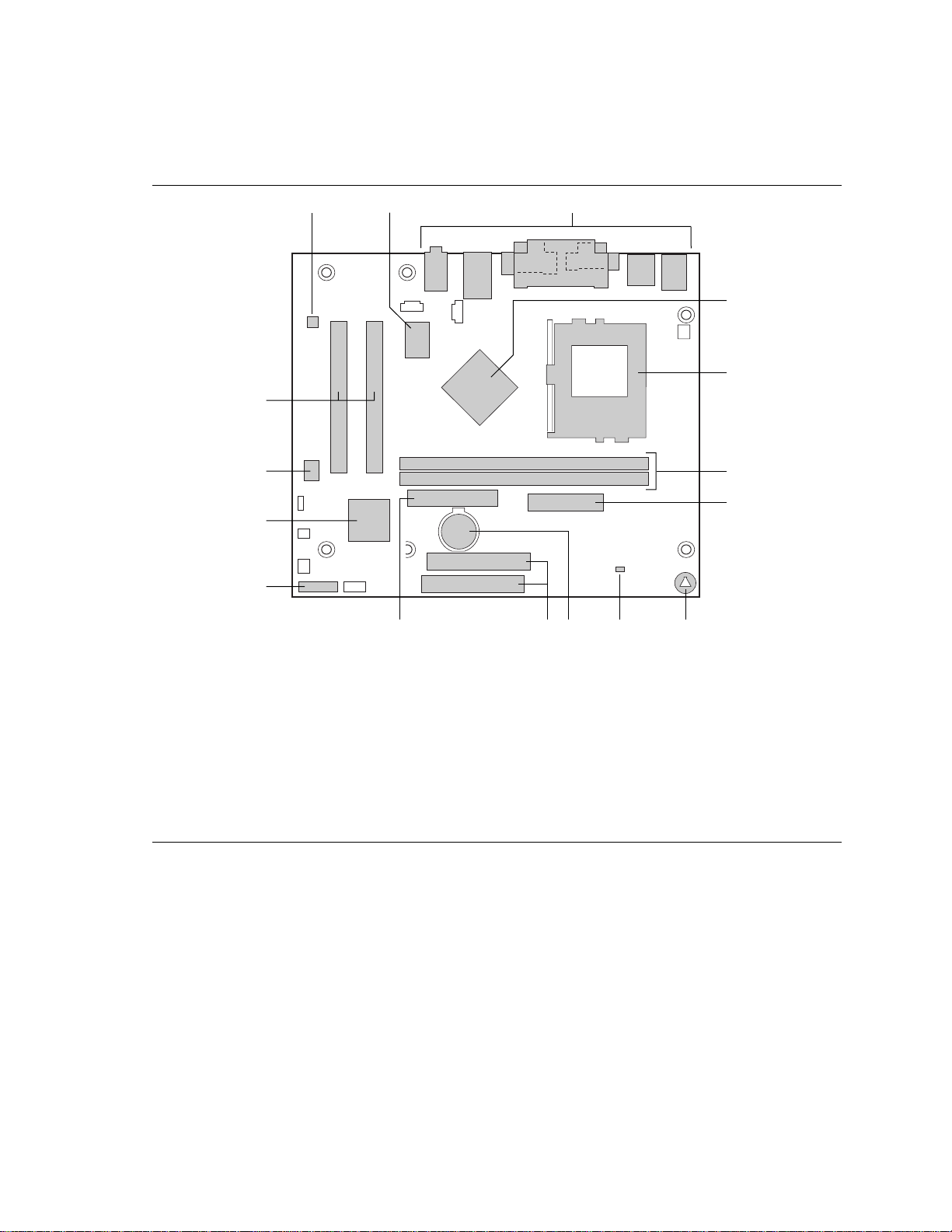
Figure 1 shows the location of the major components on the D810E2CB board.
M
A B
C
D
E
P
O
F
G
N
L
K J HI
OM11019
A CS4201 Audio Codec I Hardwaremonitor
B SMSC LPC47M102 I/O Controller J Battery
C Back panel connectors K IDE connectors
D Intel 82810E GMCH (Graphics/Memory Controller Hub) L Diskette drive connector
E Processor socket M Front panel connector
F DIMM sockets N Intel 82801BA ICH2 (I/O Controller Hub)
G Power connector O SST 49LF004A 4M Mbit Firmware Hub
H Speaker P PCI bus add-in card connectors
Figure 1. D810E2CB Board Components
14
Page 15
1.1.4 Block Diagram
Figure 2 is a block diagram of the major functional areas of the D810E2CB board.
Product Description
Processor
Socket
DIMM Banks
0and1
VGA Port
Hardware
Monitor
100 MHz
SDRAM
Bus
Primary/
SecondaryIDE
66/100/133 MHz
SystemBus
82810E
Graphics Memory
Controller Hub
(GMCH)
Display
Interface
SMBus
ATA-66/100
810E Chipset
AHA
Bus
82801BA
I/O Controlle rHub
(ICH2)
CSMA/CD
Unit
Interface
USB
LPC
Bus
LPC I/O
Controller
Physical
Laye r
Interface
USB Ports 0 and1
USB Ports 2 and3
SST 49LF004A
Firmw are Hub
(FWH)
DisketteDrive
Connector
Serial Port
Parallel Port
PS/2 Mouse
PS/2 Keyboard
LAN
Connector
(optional)
PCISlot1
PCISlot2
= connector or socket
PCI Bus
AC Link
Figure 2. Block Diagram
CS4201
Audio
Code c
CD-ROM
Line In
Line Out
Mic In
Telephony
OM11130
15
Page 16

Intel Desktop Board D810E2CB Technical Product Specification
1.2 Online Support
To find information about… Visit this World Wide Web site:
Intel’s D810E2CB board under “Product Info” or
“Customer Support”
Processor data shee ts http://www.intel.com/design/litcentr
Proper date access in systems with Intel
motherboards
ICH2 addressing http://developer.intel.com/design/chipsets/datashts
Custom splash screens http://intel.com/design/motherbd/gen_indx.htm
Audio softwareand utilities http://www.intel.com/design/motherbd
LAN software and drivers http://www.intel.com/design/motherbd
®
http://www.intel.com/design/motherbd
http://support.intel.com/support/motherboards/deskto
p
http://support.intel.com/support/year2000
1.3 Design Specifications
Table 3 lists the specifications applicable to the D810E2CB board.
Table 3. Specifications
Reference
Name
AC ‘97
ACPI
AGP
AMI BIOS
APM
ATA-3
Specification
Title
Audio Codec ‘97
Advanced Configuration
and Power Interface
Specification
Accelerated Graphics Port
Interface Specification
(2X only)
American Megatrends
BIOS Specification
Advanced Power
Management Specification
Information Technology AT Attachment-3 Interface,
X3T10/2008D
Version, Revision Date,
and Ownership
Version 2.1,
May 1998,
Intel Corporation.
Version 1.0b,
July 1, 1998,
Intel Corporation,
Microsoft Corporation,
and Toshiba Corporation.
Version 2.0,
May 4, 1998,
Intel Corporation.
AMIBIOS99,
1999
American Megatrends, Inc.
Version 1.2,
February 1996,
Intel Corporation
and Microsoft Corporation.
Version 6,
October 1998,
ASC X3T10.
This specification is
available from:
ftp://download.intel.com/
pc-supp/platform/ac97
http://www.teleport.com/~acpi/
the Accelerated Graphics
Implementers Forum at:
http://www.agpforum.org/
http://www.amibios.com, or
http://www.ami.com/download
/
amibios99.pdf
http://www.microsoft.com/hwd
ev/busbios/amp_12.htm
ATA Anonymous FTP Site:
ftp://www.dt.wdc.com/ata/
ata-3/
continued
16
Page 17

Table 3. Specifications (continued)
Product Description
Reference
Name
ATAPI
Specification
Title
Information
Technology AT
Attachment with
Packet Interface
Extensions
T13/1153D
ATX
El Torito
ATX Specification
Bootable CD-ROM
format specification
FlexATX FlexATX Addendum to
the microATX
Specification,
Version 1.0
LPC
Low Pin Count
Interface Specification
MicroATX
microATX
Motherboard Interface
Specification
SFX Power Supply
Design Guide
PCI
PCI Local Bus
Specification
PCI Bus Power
Management Interface
Specification
Plug and Play
Plug and Play BIOS
Specification
SDRAM
DIMMs
(64- and 72bit)
PC SDRAM
Unbuffered DIMM
Specification
PC SDRAM DIMM
Specification
PC Serial Presence
Detect (SPD)
Specification
Version, Revision Date and
Ownership
Version 18,
August 19, 1998,
Contact: T13 Chair, Seagate
Technology.
Version 2.01,
February 1997,
Intel Corporation.
Version 1.0,
January 25, 1995,
Phoenix Technologies Ltd.
and IBM Corporation.
Version 1.0
March 1999,
Intel Corporation.
Version 1.0,
September 29, 1997,
Intel Corporation.
Version 1.0, December 1997,
Intel Corporation.
Version 1.0, December 1997,
Intel Corporation.
Version 2.2,
December 18, 1998,
PCI Special Interest Group.
Version 1.1,
December 18, 1998,
PCI Special Interest Group.
Version 1.0a,
May 5, 1994,
Compaq Computer Corp.,
Phoenix Technologies Ltd., and
Intel Corporation.
Version 1.0,
February 1998,
Intel Corporation.
Version 1.5,
November 1997,
Intel Corporation.
Version 1.2A,
December 1997,
Intel Corporation.
This specification is
available from:
T13 Anonymous FTP
Site:
ftp://fission.dt.wdc.com/
x3t13/project/
d1153r18.pdf
http://developer.intel.com/
design/motherbd/atx.htm
the Phoenix Web site at:
http://www.ptltd.com/
techs/specs.html
http://www.teleport.com/
~ffsupprt/spec/
FlexATXaddn1_01.pdf
http://www.intel.com/
design/chipsets/industry/
lpc.htm
http://www.teleport.com/
~ffsupprt/spec/
http://www.teleport.com/
~ffsupprt/spec/microatx /
sfx11_ps.pdf
http://www.pcisig.com/
http://www.pcisig.com/
ftp://download.intel.com/
ial/wfm/bio10a.pdf
http://www.intel.com/
technology/memory/
http://www.intel.com/
technology/memory/
http://www.intel.com/
technology/memory/
continued
17
Page 18

Intel Desktop Board D810E2CB Technical Product Specification
Table 3. Specifications (continued)
Reference
Name
SMBIOS
UHCI
USB
WfM
Specification
Title
System Management
BIOS
Universal Host Controller
Interface Design Guide
Universal Serial Bus
Specification
Wired for Management
Baseline
Version, Revision Date and
Ownership
Version 2.3.1,
August 12, 1998,
Award Software International Inc.,
Dell Computer Corporation,
Hewlett-Packard Company,
Intel Corporation,
International Business Machines
Corporation,
Phoenix Technologies Limited,
American Megatrends Inc.,
SystemSoft Corporation, and
Compaq Computer Corporation.
Version 1.1,
March 1996,
Intel Corporation.
Version 1.1,
September 23, 1998,
Compaq Computer Corporation,
Intel Corporation,
Microsoft Corporation, and
NEC.
Version 2.0,
December 18, 1998,
Intel Corporation.
This specification is
available from:
http://developer.intel.com/
ial/wfm/wfm20/design/
smbios/index.htm
http://www.usb.org/
developers
http://www.usb.org/
developers
http://developer.intel.com/
ial/WfM/wfmspecs.htm
18
Page 19

Product Description
1.4 Processor
CAUTION
The D810E2CB board supports processors that draw a maximum of 22 A. Using a processor that
draws more than 22 A can damage the processor, the board, and the power supply. See the
processor’s data sheet for current usage requirements.
CAUTION
Before installing or removing the processor, make sure that AC power has been removed by
unplugging the power cord from the computer. Failure to do so could damage the processor and
the board.
The D810E2CB board supports either an Intel PentiumIII processor (FCPGA package), or an Intel
Celeron processor (PGA package) as shown in Table 4. The system bus frequency is automatically
selected.
Table 4. Supported Processors
Processor Type Processor Designation System Bus Frequency L2 Cache Size
Pentium III processors 500E, 550E, 600E, 650, 700,
750, 800, and 850 MHz
533B, 600EB, 667, 733,
800EB, 866, and 933 MHz
1.0B GHz 133 MHz 256 KB
Celeron processors 800 MHz 100 MHz 128 KB
400, 433, 466, 500, 533,
533A, 566A, 600, 633, 667,
700, 733, and 766 MHz
100 MHz 256 KB
133 MHz 256 KB
66 MHz 128 KB
All supported onboard memory can be cached, up to the cachability limit of the processor.
For information about Refer to
Processor support for the D810E2CB board http://support.intel.com/support/motherboards/deskto
p
Processor data shee ts http://www.intel.com/design/litcentr
19
Page 20

Intel Desktop Board D810E2CB Technical Product Specification
1.5 System Memory
NOTE
✏
To be compliant with applicable Intel®SDRAM memory specifications, the D810E2CB board
should be populated with DIMMs that support the Serial Presence Detect (SPD) data structure. If
your memory modules do not support SPD, the BIOS will attempt to configure the memory
controller for normal operation; however, the DIMMs may not function at their optimum speed.
CAUTION
Before installing or removing memory, make sure that AC power has been removed by unplugging
the power cord from the computer. Failure to do so could damage the memory and the board.
CAUTION
Because the main system memory is also used as video memory, the board r equires 100 MHz
SDRAM DIMMs even though the processor’s system bus speed is 66 MHz. It is highly
recommended that SPD DIMMs be used, since this allows the BIOS to read the SPD data and
program the chipset to accurately configure memory settings for optimum performance. If nonSPD memory is installed, the BIOS will attempt to correctly configure the memory settings, but
performance and reliability may be impacted.
The D810E2CB board has two DIMM sockets. The minimum memory size is 64 MB and the
maximum memory size is 512 MB. The BIOS automatically detects memory type, size, and speed.
Memory can be installed in one or both sockets. Memory size can vary between sockets.
The D810E2CB board supports the following memory features:
• 3.3 V, 168-pin DIMMs with gold-plated contacts
• 100 MHz SDRAM
• Serial Presence Detect (SPD) or non-SPD memory (BIOS recovery requires SPD DIMMs)
• Non-ECC (64-bit) memory
• Unbuffered single- or double-sided DIMMs
The board is designed to support DIMMs in the configurations listed in Table 5 below.
Table 5. System Memory Configuration
DIMM Size Non-ECC Configuration
16 MB 2 Mbit x 64
32 MB 4 Mbit x 64
64 MB 8 Mbit x 64
128 MB 16 Mbit x 64
256 MB 32 Mbit x 64
20
For information about Refer to
PC Serial Presence Detect Specification
The
Obtaining copies of PC SDRAM specifications http://www.intel.com/design/pcisets/memory
Table 3, page 16
Page 21
Product Description
1.6 Intel®810E Chipset
The Intel 810E chipset consists of the following devices:
• 82810E Graphics Memory Controller Hub (GMCH) with Accelerated Hub Architecture (AHA)
bus
• 82801BA I/O Controller Hub (ICH2) with AHA bus
• SST 49LF004A Firmware Hub (FWH)
The GMCH is a centralized controller for the system bus, the memory bus, the AGP bus, and the
Accelerated Hub Architecture interface. The ICH2 is a centralized controller for the board’s I/O
paths. The FWH provides the nonvolatile storage of the BIOS. The component combination
provides the chipset interfaces as shown in Figure 3.
ATA-66/100
66/100/133 MHz
SystemBus
Network
USB
810E Chipset
100 MHz
SDRAM Bus
82810E
Graphics Memory
Controller Hub
(GMCH)
DisplayInterface
AHA
Bus
82801BA
I/O Controller Hub
(ICH2)
LPC Bus
AC LinkPCI BusSMBus
Figure 3. Intel 810E Chipset Block Diagram
For information about Refer to
The Intel 810E chipset http://www.developer.intel.com
The resources used by the chipset Chapter 2
The chipset’s compliance with ACPI and AC ‘97 Table 3, page 16
SST 49LF004A
FirmwareHub
(FWH)
OM11129
21
Page 22

Intel Desktop Board D810E2CB Technical Product Specification
1.6.1 Direct AGP
Direct (integrated) AGP is a high-performance bus (independent of the PCI bus) for graphicsintensive applications, such as 3D applications. AGP overcomes certain limitations of the PCI bus
related to handling large amount of graphics data with the following features:
• Pipelined memory read and write operations that hide memory access latency
• Demultiplexing of address and data on the bus for nearly 100 percent bus efficiency
For information about Refer to
The location of the VGA port connector Figure 5, page 46
Obtainingthe
Accelerated Graphics Port Interface Specification
Table 3, page 16
1.6.2 USB
The ICH2 contains two separate USB controllers supporting four USB ports. One USB peripheral
can be connected to each port. For more than four USB devices, an external hub can be connected to
any of the ports. Two of the USB ports are implemented with stacked back panel connectors. The
other two are accessible via the front panel USB connector at location J8B1. The D810E2CB board
fully supports Universal Hub Controller Interface (UHCI) and uses UHCI-compatible software
drivers.
NOTE
✏
Computer systems that have an unshielded cable attached to a USB port may not meet FCC
Class B requirements, even if no device is attached to the cable. Use shielded cable that meets the
requirements for full-speed devices.
For information about Refer to
The location of the USB connectors on the back panel Figure 5, page 46
The signal names of the USB connectors on the back panel Table 21, page 47
The location of the USB connectors on the front panel Figure 8, page 58
The signal names of the USB connectors on the front panel Table 41, page 60
The USB and UHCI specifications Table 3, page 16
22
Page 23

Product Description
1.6.3 IDE Support
The ICH2’s IDE controller has two independent bus-mastering IDE interfaces that can be
independently enabled. The IDE interfaces support the following modes:
• Programmed I/O (PIO): processor controls data transfer.
• 8237-style DMA: DMA offloads the processor, supporting transfer rat es of up to 16 MB/sec.
• Ultra DMA: DMA protocol on IDE bus supportinghost and target throttling a nd transfer rates
of up to 33 MB/sec.
• Ultra ATA-66: DMA protocolon IDE bus supporting host and target throttling and transfer
rates of up to 66 MB/sec. ATA-66 protocol is similar to Ultra DMA and is device driver
compatible.
• Ultra ATA-100: DMA protocolon IDE bus allows host and target throttling. The ICH2 Ultra
ATA-100 logic can achieve read transfer rates up to 100 MB/sec and write transfer rates up to
88 MB/sec.
✏ NOTE
ATA-100 and ATA-66 use faster timings and require a specialized cable to reduce reflections,
noise, and inductive coupling.
The IDE interfaces also support ATAPI devices (such as CD-ROM drives) and ATA devices using
the transfer modes listed in Section 4.4.4.1 on page 91.
The BIOS supports logical block addressing (LBA) and extended cylinder head sector (ECHS)
translation modes. The drive reports the transfer rate and translation mode to the BIOS.
The D810E2CB board supports laser servo (LS-120) diskette technology through its IDE interfaces.
An LS-120 drive can be configured as a boot device by setting the BIOS Setup program’s Boot
menu to one of the following:
• ARMD-FDD (ATAPI removable media device – floppy disk drive)
• ARMD-HDD (ATAPI removable media device – hard disk drive)
For information about Refer to
The location of the IDE connectors Figure 7, page 54
The signal names of the IDE connectors Table 36, page 56
BIOS Setup program’s Boot menu Table 66, page 98
23
Page 24

Intel Desktop Board D810E2CB Technical Product Specification
1.6.4 Real-Time Clock, CMOS SRAM, and Battery
The real-time clock is compatiblewith DS1287 and MC146818 components. The clockprovides a
time-of-day clock and a multicentury calendar with alarm features and century rollover. The realtimeclock supports 256 bytes of battery-backed CMOS SRAM in two banks that are reservedfor
BIOS use.
A coin-cell battery powers the real-time clock and CMOS memory. When the computer is not
plugged into a wall socket, the battery has an estimated life of three years. When the computer is
plugged in, the 3.3 V standby current from the power supply extends the life of the battery. The
clock is accurate to ± 13 minutes/year at 25 ºC with 3. 3 VSB applied.
The time, date, and CMOS values can be specified in the BIOS Setup program. The CMOS values
can be returned to their defaults by using the BIOS Setup program.
NOTE
✏
If the battery and AC power fail, the last saved defaults, custom or standard, will be loaded into
CMOS SRAM at power on.
NOTE
✏
The recommended method of accessing the date in systems with Intel®desktop boards is indirectly
from the Real-Time Clock (RTC) via the BIOS. The BIOS on Intel desktop boards contains a
century checking and maintenance feature. This feature checks the two least significant digits of
the year stored in the RTC during each BIOS request (INT 1Ah) to read the date and, if less than
80 (i.e., 1980 is the first year supported by the PC), updates the century byte to 20. This feature
enables operating systems and applications using the BIOS date/time services to reliably
manipulate the year as a four-digit value.
For information about Refer to
Proper date access in systems with Intel desktop boards http://support.intel.com/support/year2000/
1.6.5 SST 49LF004A 4 Mbit Firmware Hub (FWH)
The FWH provides the following:
• System BIOS program
• System security and manageability logic that enables protection for storing and updating of
platform information
24
Page 25

1.7 I/O Controller
The SMSC LPC47M102 I/O controller provides the following features:
• 3.3 V operation
• One serial port
• One parallel port with Extended Capabilities Port (ECP) and Enhanced Parallel Port
(EPP) support
• Serial IRQ interface compatiblewith serialized IRQ support for PCI systems
• PS/2-style mouse and keyboard interfaces
• Interface for one 1.2 MB or 1.44 MB diskette drive
• Intelligent power management, including a programm able wake up event interface
• PCI power management support
The BIOS Setup program provides configuration options for the I/O controller.
For information about Refer to
SMSC LPC47M102 I/O controller http://www.smsc.com
Product Description
1.7.1 Serial Port
The D810E2CB board has one serial port connector on the back panel. The serial port’s
NS16C550-compatible UART supports data transfers at speeds up to 115.2 kbits/sec with BIOS
support. The serial port can be assigned as COM1 (3F8h), COM2 (2F8h), COM3 (3E8h), or
COM4 (2E8h).
For information about Refer to
The location of the serial port connector Figure 5, page 46
The signal names of the serial port connector Table 24, page 48
1.7.2 Parallel Port
The connector for the multimode bidirectional parallel port is a 25-pin D-Sub connector located on
the back panel. In the BIOS Setup program, the parallel port can be configured for the following:
• Output only (PC AT
• Bi-directional (PS/2 compatible)
• EPP
• ECP
For information about Refer to
The location of the parallel port connector Figure 5, page 46
The signal names of the parallel port connector Table 22, page 47
†
-compatible mode)
25
Page 26

Intel Desktop Board D810E2CB Technical Product Specification
1.7.3 Diskette Drive Controller
The I/O controller supports one diskettedrive that is compatible with the 82077 diskette drive
controller and supports both PC-AT and PS/2 modes.
For information about Refer to
The location of the diskette drive connector Figure 7, page 54
The signal names of the diskette drive connector Table 37, page 57
The supported diskette drive capacities and sizes Table 61, page 93
1.7.4 Keyboard and Mouse Interface
PS/2 keyboard and mouse connectors are located on the back panel. The +5 V lines to these
†
connectors are protected with a PolySwitch
connection after an overcurrent condition is removed.
NOTE
✏
The keyboard is supported in the bottom PS/2 connector and the mouse is supported in the top
PS/2 connector. Power to the computer should be turned off before a keyboard or mouse is
connected or disconnected.
circuit that, like a self-healing fuse, reestablishes the
The keyboard controller contains the AMI keyboard and mouse controller code, provides the
keyboard and mousecontrol functions, and supports password protectionfor power-on/reset. A
power-on/reset password can be specified in the BIOS Setup program.
For information about Refer to
The location of the keyboard and mouse connectors Figure 5, page 46
The signal names of the keyboard and mouse connectors Table 20, page 47
26
Page 27

1.8 Graphics Subsystem
The Intel 82810E GMCH graphics memory controller hub component provides the following
graphics support features:
• Integrated 2-D and 3-D graphics engines
• Integrated hardware motion compression engine
• Integrated230 MHz DAC
Table 6 lists the refresh r ates supported by the graphics subsystem.
Table 6. Supported Graphics Refresh Rates
Resolution Available Refresh Rates (Hz)
640 x 200 x 16 colors 70
640 x 350 x 16 colors 70
640 x 400 x 256 colors 60, 70, 75, 85
640 x 400 x 64 K colors 60, 70, 75, 85
640 x 400 x 16 M colors 70
640 x 480 x 16 colors 60, 72, 75, 85
640 x 480 x 256 colors 60, 70, 72, 75, 85
640 x 480 x 32 K colors 60, 75, 85
640 x 480 x 64 K colors 60, 70, 72, 75, 85
640 x 480 x 16 M colors 60, 70, 72, 75, 85
800 x 600 x 256 colors 60, 75, 85
800 x 600 x 32 K colors 60, 70, 72, 75, 85
800 x 600 x 64 K colors 60, 70, 72, 75, 85
800 x 600 x 16 M colors 60, 70, 72, 75, 85
1024 x 768 x 256 colors 60, 70, 75, 85
1024 x 768 x 32 K colors 60, 75, 85
1024 x 768 x 64 K colors 60, 70, 72, 75, 85
1024 x 768 x 16 M colors 60, 70, 72, 75, 85
1056 x 800 x 16 colors 70
1280 x 1024 x 256 colors 60, 70, 72, 75, 85
1280 x 1024 x 32 K colors 60, 75, 85
1280 x 1024 x 64 K colors 60, 70, 72, 75
1280 x 1024 x 16 M colors 60, 70, 72, 75, 85
Product Description
For information about Refer to
Obtaining graphics software and utilities http://support.intel.com/support/motherboards/desktop
27
Page 28
Intel Desktop Board D810E2CB Technical Product Specification
1.9 Audio Subsystem
The D810E2CB board includes an Audio Codec ’97 (AC ’97) compatible audio subsystem
consisting of these devices:
• Intel 82801BA ICH2 (AC link output)
• CS4201 analog codec
Figure 4 is a block diagram of the audio subsystem.
CD-ROM
82801BA
I/O ControllerHub
(ICH2)
Figure 4. Block Diagram of Audio Subsystem with CS4201 Codec
AC '97
Link
CS4201
Analog Codec
Line In
Line Out
MicIn
Modem Audio
OM11128
Features of the audio subsystem include:
• Independent channels for PCM in, PCM out, and Mic in
• 16-bit stereo I/O up to 48 kHz
• Multiple sample rates
For information about Refer to
Obtaining audio software and utilities Section1.2, page 16
1.9.1 CS4201 Analog Codec
The CS4201 is a fully AC ’97 compliant codec. T he codec's features include:
• 16-bit stereo full-duplex operation
• High quality CD-ROM input with ground sense
• Stereo line level output
• Power management support
• Full duplex variable sampling rate (7 kHz to 48 kHz) with 1 Hz resolution
†
• Phat
Stereo 3-D stereo enhancement
1.9.2 Audio Connectors
The audio connectors include the following:
• ATAPI CD-ROM (connects an internal ATAPI CD-ROM drive to the audio mixer)
• Telephony
• Line out (back panel)
• Line in (back panel)
• Mic in
28
Page 29

Product Description
For information about Refer to
The location of the ATAPI CD-ROM and telephony connectors Figure 6, page 51
The signal names of the ATAPI CD-ROM connector Table 29, page 52
The signal names of the telephony connector Table 30, page 52
The back panel audio connectors Section 2.8.1, page 46
1.10 Hardware Management Subsystem
The hardware manageme nt features enable the board to be compatible with the Wired for
Management (WfM) specification. The board has several hardware management features, including
the following:
• Fan control and monitoring
• Thermal and voltage monitoring
For information about Refer to
The WfM specification Table 3, page 16
1.10.1 Hardware Monitor Component (Optional)
The hardware monitor component provides low-cost instrumentation capabilities. The features of the
component include:
• Internal ambient temperaturesensing
• Remote thermal diode sensing for direct monitoring of processor temperature
• Power supply monitoring (+12 V, +5 V, +3.3 V, +2.5 V, 3.3 VSB, Vccp) to detect levels above
or below acceptable values
• SMBus interface
The hardware monitor component enables the board to be compatible with the Wired for
Management (WfM) specification.
For information about Refer to
The board’s compatibility with the WfM specification Table3, page 16
1.10.2 Fan Control and Monitoring
The SMSC LPC47M102 I/O controller provides two fan sense inputs and two fan control outputs.
Monitoring and control can be impleme nted using third-party software.
For information about Refer to
The functions of the fan connectors Section 1.12.3.2, page 35
The locations of the fan connectors Figure 6, page 51
The signal names of the fan connectors Section 2.8.2.1, page 51
29
Page 30

Intel Desktop Board D810E2CB Technical Product Specification
1.11 LAN Subsystem (Optional)
The Network Interface Controller subsystemconsists of the ICH2 (with integrated LAN Media
Access Controller) and a physical layer interface device. Features of the LAN subsystem include:
• PCI Bus Master interface
• CSMA/CD Protocol Engine
• Serial CSMA/CD unit interface that supports the 82562ET (10/100 Mbit/sec Ethernet) physical
layer interface device
• PCI Power Management
Supports APM
Supports ACPI technology
†
Supports Wake up from suspend state (Wake on LAN
For information about Refer to
Obtaining LAN software and drivers Section 1.2, page 16
1.11.1 Intel®82562ET Platform LAN Connect Device
technology)
The Intel 82562ET component provides a n interface to the back panel RJ-45 connector with
integrated LEDs. This physical interface may alternately be provided via the CNR connector.
The Intel 82562ET provides the following functions:
• Basic 10/100 Ethernet LAN connectivity
• Supports RJ-45 connector with status indicator LEDs on the back panel
• Full device driver compatibility
• Advanced Power Management and ACPI support
• Programmable transit threshold
• Configuration EEPROM that contains the MAC address
• Remote monitoring (alerting)
1.11.2 RJ-45 LAN Connector with Integrated LEDs
Two LEDs are built into the RJ-45 LAN connector. Table 7 describes the LED states when the
board is powered up and the LAN subsystem is operating.
Table 7. LAN Connector LED States
LED Color LED State Condition
Off 10 Mbit/sec data rate is selected.Green
On 100 Mbit/sec data rate is selected.
Yellow
Off LAN link is not established.
On (steady state) LAN link is established.
On (brighter and pulsing) The computer is communicating with another computer on
the LAN.
30
Page 31

1.12 Power Management Features
Power management is implemented at several levels, including:
• Advanced Configuration and Power Interface (ACPI)
• Advanced Power Management (APM)
• Hardware support:
Power connector
Fan connectors
Wake on LAN technology
†
Instantly Available
Wake on Ring
Resume on Ring
Wake from USB
PME# wakeup support
1.12.1 ACPI
technology
Product Description
If the board is used with an ACPI-aware operating system, the BIOS can provide ACPI support.
ACPI gives the operating system direct control over the power management and Plug and Play
functions of a computer. The use of ACPI with this board requires the support of a n operating
system that provides full ACPI functionality. ACPI features include:
• Plug and Play (including bus and device enumeration)
• Power management control of individual devices, video displays, and hard disk drives
• Methods for achieving less than 30-watt system operation in the Power On Suspend sleeping
state, and less than 5-watt system operationin the Suspend to RAM sleepingstate
• A Soft-off feature that enables the operating system to power off the computer
• Support for multiple wake up events (see Table 10 on page 33)
• Support for a front panel power and sleep mode switch.
Table 8 lists the system states based on how long the power switch is pressed, depending on how
ACPI is configured with an ACPI-aware operating system.
Table 8. Effects of Pressing the Power Switch
…and the power switch is
If the system is in this state…
Off (ACPI G2/S5 state) Less than four seconds Power on
On (ACPI G0 state) Less than four seconds Soft off/Suspend
On (ACPI G0 state) More than four seconds Fail safe power off
Sleep (ACPI G1 state) Less than four seconds Wake up
Sleep (ACPI G1 state) More than four seconds Power off
pressed for …the system enters this state
For information about Refer to
The board’s compliance level with ACPI Table 3, page 16
31
Page 32

Intel Desktop Board D810E2CB Technical Product Specification
1.12.1.1 System States and Power States
Under ACPI, the operating system directs all system and device power state transitions. The
operating system puts devices in and out of low-power states based on user preferences and
knowledge of how devices are being used by applications. Devices that are not being used can be
turned off. The operating system uses information from applications and user settings to put the
system as a whole into a low-power state.
Table 9 lists the power sta t es supported by the board along with the associated system power targets.
See the ACPI specification for a complete description of the various system and power states.
Table 9. Power States and Targeted System Power
Global States Sleeping States CPU States Device States Targeted System
Power*
G0 - working state S0 - working C0 - working D0 - working
state
G1 - sleeping state S1 - CPU stopped C1 - stop grant D1, D2, D3 -
device
specification
specific.
G1 - sleeping state S3 - Suspend-to-
RAM. Context
saved to RAM.
G2/S5 S5 - Soft off.
Context not
saved. Cold boot
is required.
G3 - mechanical off.
(AC power is
disconnected from
the computer.)
* Totalsystempower is dependent on the system configuration, including peripherals poweredby the system chassis’ power
supply.
** Dependent on the standbypower consumption of wake-up devices used in the system.
No power to the
system.
No power D3 - no power
except for
wake up logic.
No power D3 - no power
except for
wake up logic.
No power D3 - no power
for wakeup
logic, except
when provided
by battery or
external
source.
Full power > 30 W
5W<power<30W
Power < 5 W **
Power < 5 W **
No power to the system
so that service can be
performed.
32
Page 33

Product Description
1.12.1.2 Wake-up Devices and Events
Table 10 lists the devices or specific events that can wake the computer from specific states.
Table 10. A CPI Wake-up Devices and Events
These devices/events can wake-up the computer… …from this state
Power switch S1, S3, S5
RTC alarm S1, S3, S5
LAN S1, S3
PME# S1, S3
USB S1, S3
PS/2 S1, S3
1.12.1.3 Plug and Play
In addition to power management, ACPI provides controls and information so that the operating
system can facilitate Plug and Play device enumeration and configuration. ACPI is used only to
enumerate and configure devices that do not have other hardware standards for enumeration and
configuration. PCI devices on a desktop board, for example, are not enumerated by ACPI.
1.12.2 APM
APM makes it possible for the computer to enter an energy saving standby mode. The standby mode
can be initiated in the following ways:
• Time-out period specified in the BIOS Setup program
• Suspend/Resume switch connected to the front panel sleep connector
• From the operating system, such as the Suspend menu item in Windows 98 SE
In standby mode, the board can reduce power consumption by spinning down hard drives, and
†
reducing power to or turning off VESA
be enabled or disabled in the BIOS Setup program.
While in standby mode, the system retains the ability to respond to external interrupts and service
requests, such as incoming faxes or network messages. Any keyboard or mouse activity brings the
system out of standby mode and immediately restores power to the monitor.
The BIOS enables APM by default, but the operating system must support an APM driver for the
power-management features to work. For example, Windows 98 SE supports the powermanagement features upon detecting that APM is enabled in the BIOS.
Table 11 lists the devices or specific events that can wake the computer from specific states.
DPMS-compliant monitors. Power-manageme nt mode can
33
Page 34

Intel Desktop Board D810E2CB Technical Product Specification
Table 11. A PM Wake-up Devices and Events
These devices/events can wake up the computer… …from this state
Power switch Soft-off
RTC alarm* Soft-off, suspend
LAN Soft-off, suspend
PME# Soft-off, suspend
USB Suspend
PS/2 Suspend
* Unattended WakeMode – display will be video BIOS string only
For information about Refer to
Enabling or disabling power management in the BIOS Setup program Section 4.6, page 97
The board’s compliance level with APM Table 3, page 16
1.12.3 Hardware Support
CAUTION
If Wake on LAN and Instantly Available technology features are used, the power supply must be
capable of providing adequate +5 V standby current. Failure to provide adequate standby current
can damage the power supply. The total amount of standby current required depends on the wake
devices supported and manufacturing options. Refer to Section 2.11.2 on page 66 for additional
information.
The board provides several hardware features that support power management, including:
• Power connector
• Fan connectors
• Wake on LAN technology
• Instantly Available technology
• Wake on Ring
• Resume on Ring
• Wake from USB
• PME# wakeup support
Wake on LAN technology and Instantly Available technology require power from the +5 V standby
line. The sections discussing these features describe the incremental standby power requirements for
each.
Wake on Ring and Resume on Ring enable telephony devices to access the computer when it is in a
power-managed state. The method used depends on the type of telephony device (external or
internal) and the ACPI or APM state beingused.
NOTE
✏
The use of Wake on Ring, Resume on Ring, and Wake from USB technologies from an ACPI state
require the support of an operating system that provides full ACPI functionality.
34
Page 35

Product Description
1.12.3.1 Power Connector
When used with an ATX-compliant power supply that supports remotepower on/off, the D810E2CB
board can turn off the system power through software control.
With soft-off enabled, if power to the computer is interrupted by a power outage or a disconnected
power cord, when power resumes, the computer returns to the power state it was in before power
was interrupted (on or off).
For information about Refer to
The location of the power connector Figure 6, page 51
The signal names of the power connector Table 32, page 53
The ATX specification Table 3, page 16
The MicroATX specification and the SFX Power Supply Design Guide Table 3, page 16
1.12.3.2 Fan Connectors
Table 12 describes the functions of the fan connectors.
Table 12. Fan Connector Descriptions
Connector Function
Processor fan (fan 1) Provides +12 V DC for a processor fan or active fan heatsink.
Chassis fan (fan 2) Provides +12 V DC for a system or chassis fan.
For information about Refer to
The location of the fan connectors Figure 6, page 51
The signal names of the processor fan connector Table 31, page 52
The signal names of the chassis fan connector Table 34, page 53
1.12.3.3 Wake on LAN T echnology
CAUTION
For Wake on LAN technology, the 5-V standby line for the power supply must be capable of
providing adequate +5 V standby current. Failure to provide adequate standby current when
implementing Wake on LAN technology can damage the power supply. Refer to Section 2.11.2 on
page 66 for additional information.
Wake on LAN technology enables remote wakeup of the computer through a network. The LAN
subsystem monitors network traffic at the Media Independent Interface. Upon detecting a Magic
†
Packet
D810E2CB board supports Wake on LAN technology through the PCI bus PME# signal.
frame, the LAN subsystem asserts a wakeup signal that powers up the computer. The
35
Page 36

Intel Desktop Board D810E2CB Technical Product Specification
1.12.3.4 Instantly Available T echnology
CAUTION
For Instantly Available technology, the 5-V standby line for the power supply must be capable of
providing adequate +5 V standby current. Failure to provide adequate standby current when
using this feature can damage the power supply. Refer to Section 2.11.2 on page 66 for additional
information.
Instantly Available technology enables the board to enter the ACPI S3 (Suspend-to-RAM) sleepstate. While in the S3 sleep-state, the computer will appear to be off. The power supply appears to
be off, the fans are off, and the front panel power LED will be yellow (unless a single color LED is
installed, in which case, it will be off.) When signaled by a wake-up device or event, the system
quickly returns to its last known wake state. Table 10 on page 33 lists the devices and events that
can wake the computer from the S3 state.
The D810E2CB board supports the PCI Bus Power Management Interface Specification.For
information on the versions of this specification, see Section 1.3. Add-in boards that also support
this specification can participate in power management and can be used to wake the computer.
The use of Instantly Available technology requires operating system support and PCI 2.2 compliant
add-in cards and drivers.
1.12.3.5 Wake on Ring
NOTE
✏
Wake on Ring requires the use of a modem (external USB, or modem connected to serial port A)
that supports the Wake on Ring feature.
The operation of Wake on Ring can be summarized as follows:
• Powers up the computer from the ACPI S5 state or from APM soft-off mode
• Requires two calls to access the computer:
First call restores the computer from an ACPI S5 state or powers up the computer from
APM soft-off mode.
Second call enables access (when the appropriate software is loaded).
• Detects incoming calls for external USB modems. The USB bus is monitored for the
RING_DETECT signal.
Table 13 outlines wake on ring support for modems.
Table 13. Wake on Ring Support for Modems
State USB Modem Serial Port Modem PCI Bus Modem (via PME#)
S1 Refer to Section 1.12.3.6 Refer to Section 1.12.3.6 Supported
S3 Supported Supported Supported
S5 Not supported Supported Not supported
Soft-off Not supported Supported Supported
Suspend Refer to Section 1.12.3.6 Refer to Section 1.12.3.6 Supported
36
Page 37

Product Description
1.12.3.6 Resume on Ring
The operation of Resume on Ring can be summarized as follows:
• Resumes operation from the ACPI S1 state or APM suspend mode
• Requires only one call to access the computer
• Detects incoming call similarly for external and internal modems
1.12.3.7 Wake from USB
USB bus activity wakes the computer from an ACPI S1 or S3 state or APM suspend mode.
NOTE
✏
Wake from USB requires the use of a USB peripheral that supports Wake from USB. Wake from
USB is not supported in APM soft-off mode.
1.12.3.8 PME# Wakeup Support
When the PME# signal on the PCI bus is asserted, the computer wakes from an ACPI S1 or S3
state.
37
Page 38

Intel Desktop Board D810E2CB Technical Product Specification
38
Page 39

2 Technical Reference
What This Chapter Contains
2.1 Introduction................................................................................................................39
2.2 Memory Map..............................................................................................................39
2.3 I/O Map...................................................................................................................... 40
2.4 DMA Channels...........................................................................................................42
2.5 PCI Configuration Space Map....................................................................................42
2.6 Interrupts....................................................................................................................43
2.7 PCI Interrupt Routing Map .........................................................................................44
2.8 Connectors ................................................................................................................45
2.9 Jumper Block.............................................................................................................61
2.10 Mechanical Considerations........................................................................................63
2.11 Electrical Considerations............................................................................................65
2.12 Thermal Considerations.............................................................................................67
2.13 Reliability....................................................................................................................68
2.14 Environmental............................................................................................................69
2.15 Regulatory Compliance..............................................................................................70
2.1 Introduction
Sections 2.2 – 2.6 contain several standalone tables. Table 14 describes the system memory map,
Table 15 shows the I/O map, Table 16 lists the DMA channels, Table 17 defines the PCI
configuration space map, and Table 18 describes the interrupts. The remaining sections in this
chapter are introduced by text found with their respective section headings.
2.2 Memory Map
Table 14. System Memory Map
Address Range (decimal) Address Range (hex) Size Description
1024 K - 524288 K 100000 - 1FFFFFFF 511 MB Extended memory
960 K - 1024 K F0000 - FFFFF 64 KB Runtime BIOS
896 K - 960 K E0000 - EFFFF 64 KB Reserved
800 K - 896 K C8000 - DFFFF 96 KB Available high DOS memory (open
to PCI bus)
640 K - 800 K A0000 - C7FFF 160 KB Video memory and BIOS
639 K - 640 K 9FC00 - 9FFFF 1 KB Extended BIOS data (movable by
memory manager software)
512 K - 639 K 80000 - 9FBFF 127 KB Extended conventional memory
0 K - 512 K 00000 - 7FFFF 512 KB Conventional memory
39
Page 40

Intel Desktop Board D810E2CB Technical Product Specification
2.3 I/O Map
Table 15. I/O Map
Address (hex) Size Description
0000 - 000F 16 bytes DMA controller
0020 - 0021 2 bytes Programmable Interrupt Controller (PIC)
0040 - 0043 4 bytes System timer
0060 1 byte Keyboard controller byte – reset IRQ
0061 1 byte System speaker
0064 1 byte Keyboard controller, CMD/STAT byte
0070 - 0071 2 bytes System CMOS / Real-Time Clock (RTC)
0072 - 0073 2 bytes System CMOS
0080 - 008F 16 bytes DMA controller
0092 1 byte Fast A20 and PIC
00A0 - 00A1 2 bytes PIC
00B2 - 00B3 2 bytes Reserved
00C0 - 00DF 32 bytes DMA
00F0 1 byte Numeric data processor
0170 - 0177 8 bytes Secondary IDE channel
01F0 - 01F7 8 bytes Primary IDE channel
02E8 - 02EF
02F8 - 02FF
0376 1 byte Secondary IDE channel command port
0377, bits 6:0 7 bits Secondary IDE channel status port
03B0 - 03BB 12 bytes Intel 82810E – DC100 Graphics/Memory Controller Hub (GMCH)
03C0 - 03DF 32 byte Intel 82810E – Graphics/Me mory Controller Hub (GMCH)
03E8 - 03EF 8 bytes COM3
03F6 1 byte Primary IDE channel command port
03F8 - 03FF 8 bytes COM1
1
8 bytes COM4/video (8514A)
1
8bytes COM2
continued
40
Page 41

Table 15. I/O Map (continued)
Address (hex) Size Description
04D0 - 04D1 2 bytes Edge/level triggered PIC
0CF8 - 0CFB
3
0CF9
0CFC - 0CFF 4 bytes PCI configuration data register
E800 - E8FF 256 bytes ICH2 Audio controller
EF00 - EF3F 64 bytes ICH2 Audio bus master
FFA0 - FFA7 8 bytes Primary bus master IDE registers
FFA8 - FFAF 8 bytes Secondary bus master IDE registers
96 contiguous bytes starting on a
128-byte divisible boundary
64 contiguous bytes starting on a
64-byte divisible boundary
64 contiguous bytes starting on a
64-byte divisible boundary
32 contiguous bytes starting on a
32-byte divisible boundary
32 contiguous bytes starting on a
32-byte divisible boundary
16 contiguous bytes starting on a
16-byte divisible boundary
4096 contiguous bytes starting on
a 4096-byte divisible boundary
96 contiguous bytes starting on a
128-byte divisible boundary
Notes:
1. Default, but can be changed to another address range
2. Dword accessonly
3. Byteaccess only
2
4 bytes PCI configuration address register
1 byte Turbo and reset control register
ICH2 (ACPI + TCO)
D810E2CB Board Resource
ICH2 LAN controller
ICH2 (USB Controller #1)
ICH2 (USB Controller #2)
ICH2 (SMBus)
Intel 82801BA PCI Bridge
LPC47M102 I/O controller
Technical Reference
✏✏✏✏ NOTE
Some additional I/O addresses are not available due to ICH2 addresses aliasing.
For information about Refer to
ICH2 addressing Section 1.2, page 16
41
Page 42

Intel Desktop Board D810E2CB Technical Product Specification
2.4 DMA Channels
Table 16. DMA Channels
DMA Channel Number Data Width System Resource
0 8- or 16-bits Open
1 8- or 16-bits Open
2 8- or 16-bits Open
3 8- or 16-bits Open / ECP
4 Reserved - cascade channel
5 16-bits Open
6 16-bits Open
7 16-bits Open
2.5 PCI Configuration Space Map
Table 17. PCI Configuration Space Map
Bus
Number (hex)
00 00 00 Memory controller of Intel 82810E component
00 01 00 Graphics controller of Intel 82810E component
00 1E 00 Link to PCI bridge
00 1F 00 PCI-to-LPC bridge
00 1F 01 IDE controller
00 1F 02 USB controller #1
00 1F 03 SMBus controller
00 1F 04 USB controller #2
00 1F 05 AC ’97 audio controller
00 1F 06 AC ’97 modem controller
01 08 00 ICH2 LAN controller (optional)
01 09 00 PCI bus connector 1 (J3B1)
01 0A 00 PCI bus connector 2 (J3A2)
Device
Number (hex)
Function
Number (hex) Description
42
Page 43

2.6 Interrupts
Table 18. Interrupts
IRQ System Resource
NMI I/O channel check
0 Reserved, interval timer
1 Reserved, keyboard buffer full
2 Reserved, cascade interrupt from slave PIC
3COM2*
4COM1*
5 LAN / User available
6 User available
7 LPT1 (Parallel port if present, or else, user available) / ECP
8 Real-time clock
9 Reserved for ICH2 system management bus / Audio
10 User available
11 User available
12 Onboard mouse port (if present, or else, user available)
13 Reserved, math coprocessor
14 Primary IDE (if present, or else, user available)
15 Secondary IDE (if present, or else, user available)
* Default, but can be changed to another IRQ
Technical Reference
43
Page 44

Intel Desktop Board D810E2CB Technical Product Specification
2.7 PCI Interrupt Routing Map
This section describes interrupt sharing and how the interrupt signals are connected between the
onboard PCI devices. The PCI specification shows how interrupts can be shared between devices
attached to the PCI bus. In most cases, the small amount of latency added by interrupt sharing does
not affect the operation or throughput of the devices.
The ICH2 PCI-to-LPC bridge has eight programm able interrupt request (PIRQ) input signals. All
PCI interrupt sources connect to one of these PIRQ signals. Because there are only eight signals,
some PCI interrupt sources are mechanically tied together on the D810E2CB board and therefore
share the same interrupt.
Table 19 lists the PIRQ signals and shows how the signals are connected to the onboard PCI
interrupt sources.
For example, using as a reference, assume an add-in card using INTA is plugged into PCI bus
connector 2. In PCI bus connector 2, INTA is connected to PIRQF, which is already connected to
the SMBus. The add-in card in PCI bus connector 2 now shares interrupts with these onboard
interrupt sources.
Table 19. PCI Interrupt Routing Map
ICH2 PIRQ Signal Name
PCI Interrupt Source
ICH2 USB controller INTD to PIRQD
SMBus controller INTB
ICH2 USB controller INTC to PIRQH
ICH2 Audio INTB
ICH2 LAN INTA to PIRQE
PCI Bus Connector 1 (J3B1) INTA INTB INTC INTD
PCI Bus Connector 2 (J3A2) INTD INTA INTB INTC
NOTE
✏
The ICH2 can connect each PIRQ line internally to one of the IRQ signals (3, 4, 5, 6, 7, 10, 11, 14,
and 15). Typically, a device that does not share a PIRQ line will have a unique interrupt.
However, in certain interrupt-constrained situations, it is possible for two or more of the PIRQ
lines to be connected to the same IRQ signal.
PIRQC PIRQF PIRQG PIRQB Other
44
Page 45

Technical Reference
2.8 Connectors
CAUTION
Only the back panel connectors of the board and the front panel USB connectors have overcurrent
protection. The other internal board connectors are not overcurrent protected and should connect
only to devices inside the computer chassis such as fans and internal peripherals. Do not use these
connectors for powering devices external to the computer chassis. A fault in the load presented by
an external device may result in a high output current that could damage the D810E2CB board,
the interconnecting cable, and the external device itself.
This section describes the D810E2CB board’s connectors. The connectors can be divided into the
following three groups:
• Back panel I/O connectors (see page 46)
PS/2 keyboard and mouse
USB (two)
Parallel port
VGA
Serial port
LAN
Audio (Line out, Line in, and Mic in)
• Internal I/O connectors (see page 50)
Audio (ATAPI CD-ROM and telephony)
Fans (2)
Power
Chassis intrusion
Add-in boards (two PCI bus connectors)
IDE (two)
Diskette drive
• External I/O connectors (see page 58)
Front panel (power/sleep/message-waiting LED, power switch, hard drive activity LED,
reset switch, and infrared port)
Front panel USB
45
Page 46

Intel Desktop Board D810E2CB Technical Product Specification
2.8.1 Back Panel Connectors
Figure 5 shows the location of the back panel connectors.
A
C
B
D
Item Description Connector Color For additional Information…
A PS/2 mouse port Lime green See Table 20, page 47
B PS/2 keyboard port Purple See Table 20, page 47
C USB port 0 Black See Table 21, page 47
D USB port 1 Black See Table 21, page 47
E Parallel port Burgundy See Table 22, page 47
F VGA Blue See Table 23, page 48
G Serial port A Teal See Table 24, page 48
H LAN (optional) Not color specific See Table 25, page 48
I Audio Line In Light blue SeeTable 26, page 49
J Audio Line Out Lime green See Table 27, page 49
K Mic In Pink See Table 28, page 49
Figure 5. Back Panel Connectors
E
F
HG
I
J
K
OM11021
NOTE
✏
The back panel audio line out connector is designed to power headphones or amplified speakers
only. Poor audio quality may occur if passive (non-amplified) speakers are connected to this
output.
46
Page 47

Table 20. PS/2 Mouse/Keyboard
Pin Signal Name
1Data
2 Not connected
3 Ground
4Fused+5V
5Clock
6 Not connected
Table 21. USB Ports 0 and 1
Pin Signal Name
1+5V(fused)
2 USBP0# / USBP1#
3 USBP0 / USBP1
4 Ground
Technical Reference
Table 22. Parallel Port
Pin Standard Signal Name E CP Signal Name EPP Signal Name
1 STROBE# STROBE# WRITE#
2 PD0 PD0 PD0
3 PD1 PD1 PD1
4 PD2 PD2 PD2
5 PD3 PD3 PD3
6 PD4 PD4 PD4
7 PD5 PD5 PD5
8 PD6 PD6 PD6
9 PD7 PD7 PD7
10 ACK# ACK# INTR
11 BUSY BUSY#, PERIPHACK WAIT#
12 PERROR PE, ACKREVERSE# PE
13 SELECT SELECT SELECT
14 AUDOF D# AUDOFD#, HOSTACK DATASTB#
15 FAULT# FAULT#, PERIPHREQST# FAULT#
16 INIT# INIT#, REVERSERQST# RESET#
17 SLCTIN# SLCTIN# ADDRSTB#
18 – 25 GND GND GND
47
Page 48

Intel Desktop Board D810E2CB Technical Product Specification
Table 23. VGA Port
Pin Signal Name
1Red
2 Green
3Blue
4 No connect
5 Ground
6 Ground
7 Ground
8 Ground
9FusedVCC
10 Ground
11 No connect
12 MONID1
13 HSYNC
14 VSYNC
15 MONID2
Table 24. Serial Port A
Pin Signal Name
1 DCD (Data Carrier Detect)
2 SIN# (Serial Data In)
3 SOUT# (Serial Data Out)
4 DTR (Data Terminal Ready)
5 Ground
6 DSR (Data Set Ready)
7 RTS (Request to Send)
8 CTS (Clear to Send)
9 RI (Ring Indicator)
Table 25. LAN (Optional)
Pin Signal Name
1TX+
2TX3RX+
4 Ground
5 Ground
6RX7 Ground
8 Ground
48
Page 49

Table 26. Audio Line In
Pin Signal Name
Tip Audio left in
Ring Audio right in
Sleeve Ground
Table 27. Audio Line Out
Pin Signal Name
Tip Audio left out
Ring Audio right out
Sleeve Ground
Table 28. Mic In Connector
Pin Signal Name
Tip Mono in
Ring Mic bias voltage
Technical Reference
49
Page 50

Intel Desktop Board D810E2CB Technical Product Specification
2.8.2 Internal I/O Connectors
The internal I/O connectors are divided into the following functional groups:
• Audio, power, and hardware control (see page 51)
ATAPI CD-ROM
Telephony
Fans (2)
Power
Chassis intrusion
• Add-in boards and peripheral interfaces (see page 54)
PCI bus (2)
IDE (2)
Diskette drive
50
Page 51
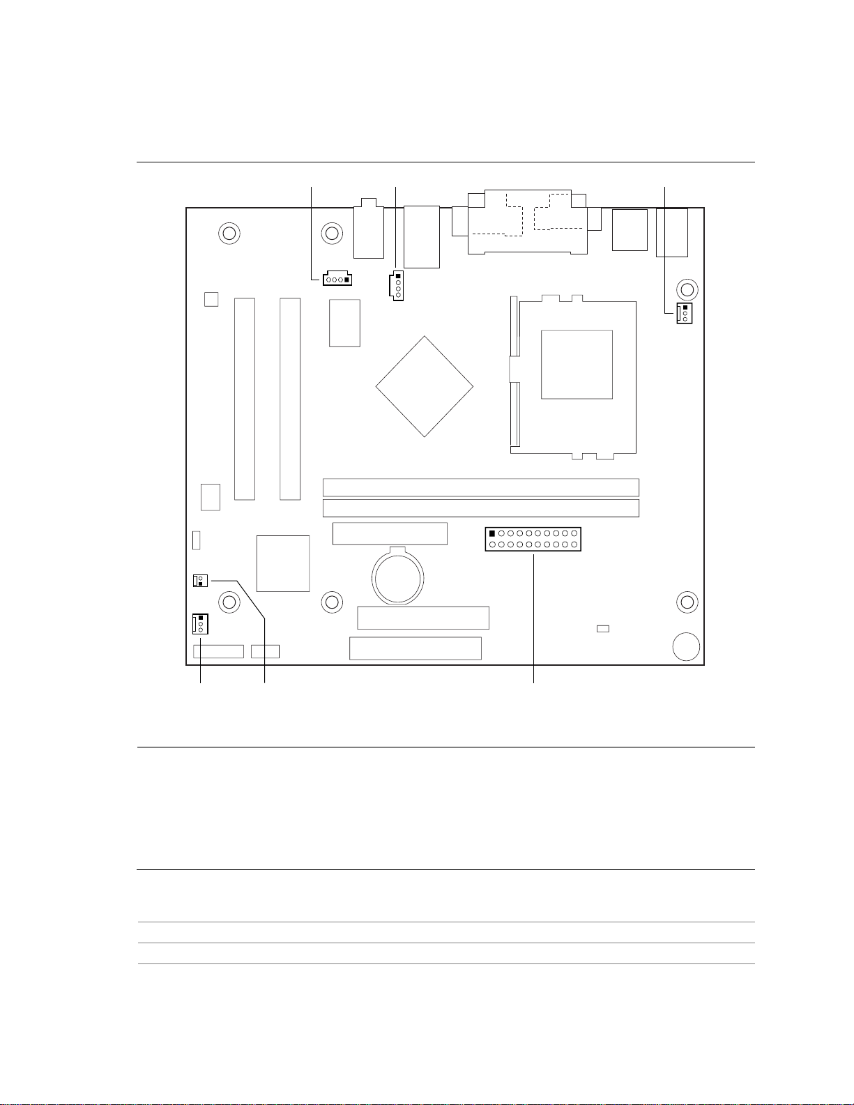
2.8.2.1 Audio, Power, and Hardware Control Connectors
Figure 6 shows the location of the audio, power, and hardware control connectors.
Technical Reference
A B
1
C
1
1
1
11
10
20
1
1
F E
D
OM11022
Item Description Reference Designator For additional information see…
A ATAPI CD-ROM J1C1 (Black) Table 29, page 52
B Telephony, ATAPI-style J2D1 (Green) Table 30, page 52
C Processor fan (Fan 1) J2J1 Table 31, page 52
D Power J6F1 Table 32, page 53
E Chassis intrusion J6A2 Table 33, page 53
F Chassis fan (Fan 2) J7A1 Table 34, page 53
Figure 6. Audio, Power, and Hardware Control Connectors
For information about… Refer to…
The power connector Section 1.12.3.1, page 35
The functions of the fan connectors Section 1.12.3.2, page 35
51
Page 52

Intel Desktop Board D810E2CB Technical Product Specification
Table 29. ATAPI CD-ROM Connector (J1C1)
Pin Signal Name
1 Left audio input from CD-ROM
2 CD audio differential ground
3 CD audio differential ground
4 Right audio input from CD-ROM
Table 30. Telephony Connector (J2D1)
Pin Signal Name
1 Analog audio mono input
2 Ground
3 Ground
4 Analog audio mono output
Table 31. Processor Fan Connector (J2J1)
Pin Signal Name
1 FAN1_PWM
2+12V
3 FAN1_TACH
52
Page 53

Technical Reference
Table 32. Power Connector (J6F1)
Pin Signal Name Pin Signal Name
1 +3.3 V 11 +3.3 V
2 +3.3 V 12 -12 V
3 Ground 13 Ground
4 +5 V 14 PS-ON# (power supply remote on/off)
5 Ground 15 Ground
6 +5 V 16 Ground
7 Ground 17 Ground
8 PWRGD (Powe r Good) 18 R eserved
9 +5 VSB 19 +5 V
10 +12 V 20 +5 V
Table 33. Chassis Intrusion Connector (J6A2)
Pin Signal Name
1 Intruder#
2 Ground
Table 34. Chassis Fan Connector (J7A1)
Pin Signal Name
1 FAN2_PWM
2+12V
3 FAN2_TACH
53
Page 54
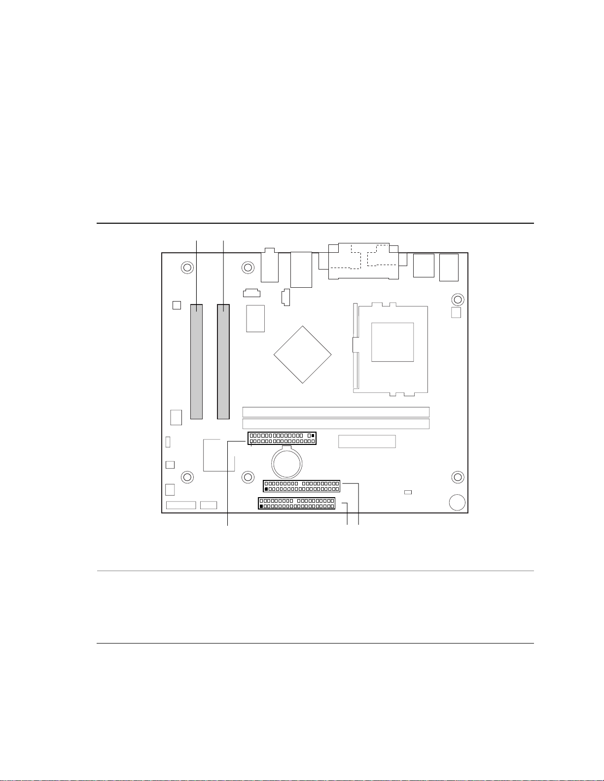
Intel Desktop Board D810E2CB Technical Product Specification
2.8.2.2 Add-in Board and Peripheral Interface Connectors
Figure 6 shows the location of the add-in board and peripheral interface connectors. Note the
following considerations for the PCI bus connectors:
• All of the PCI bus connectors are bus master capable.
• PCI bus connector 2 has SMBus signals routed to it. This enables PCI bus add-in boards with
SMBus support to access sensor data on the board. The specific SMBus signals are a s follows:
The SMBus clock line is connected to pin A40
The SMBus data line is connected to pin A41
A B
33
34
2
1
2
1
E
1
2
40
39
40
39
CD
OM11023
Item Description Reference Designator For additional information see…
A PCI bus connector 2 J3A2 Table 35, page 55
B PCI bus connector 1 J3B1 Table 35, page 55
C Secondary IDE J7E1 Table 36, page 56
D Primary IDE J8D1 Table 36, page 56
E Diskette drive J6D1 Table 37, page 57
Figure 7. Add-in Board and Peripheral Interface Connectors
54
Page 55

Technical Reference
Table 35. PCI Bus Connectors (J3A2 and J3B1)
Pin Signal Name Pin Signal Name Pin Signal Name Pin Signal Name
A1 Ground (TRST#)* B1 -12 V A32 AD16 B32 AD17
A2 +12 V B2 Ground (TCK)* A33 +3.3 V B33 C/BE2#
A3 +5 V (TMS)* B3 Ground A34 FRAME# B34 Ground
A4 +5 V (TDI)* B4 no connect (TDO)* A35 Ground B35 IRDY#
A5 +5 V B5 +5 V A36 TRDY# B36 +3.3 V
A6 INTA# B6 +5 V A37 Ground B37 DEVSEL#
A7 INTC# B7 INTB# A38 STOP# B38 Ground
A8 +5 V B8 INTD# A39 +3.3 V B39 LOCK#
A9 Reserve d B9 no connect (PRSNT1#)* A40 Reserved ** B40 PERR#
A10 +5 V (I/O) B10 Reserved A41 Reserved *** B41 +3.3 V
A11 Reserved B11 no connect (PRSNT 2#)* A42 Ground B42 SERR#
A12 Ground B12 Ground A43 PAR B43 +3.3 V
A13 Ground B13 Ground A44 AD15 B44 C/BE1#
A14 +3.3 V aux B14 Rese rved A45 +3.3 V B45 AD14
A15 RST# B15 Ground A46 AD13 B46 Ground
A16 +5 V (I/O) B16 CLK A47 AD11 B47 AD12
A17 GNT# B17 Ground A48 Ground B48 AD10
A18 Ground B18 REQ# A49 AD09 B49 Ground
A19 PME# B19 +5 V (I/O) A50 Key B50 Key
A20 AD30 B20 AD31 A51 Key B51 Key
A21 +3.3 V B21 AD29 A52 C/BE0# B52 AD08
A22 AD28 B22 Ground A53 +3.3 V B53 AD07
A23 AD26 B23 AD27 A54 AD06 B54 +3.3 V
A24 Ground B24 AD25 A55 AD04 B55 AD05
A25 AD24 B25 +3.3 V A56 Ground B56 AD03
A26 IDSEL B26 C/BE3# A57 AD02 B57 Ground
A27 +3.3 V B27 AD23 A58 AD00 B58 AD01
A28 AD22 B28 Ground A59 +5 V (I/O) B59 +5 V (I/O)
A29 AD20 B29 AD21 A60 REQ64C# B60 ACK64C#
A30 Ground B30 AD19 A61 +5 V B61 +5 V
A31 AD18 B31 +3.3 V A62 +5 V B62 +5 V
* These signals (in parentheses) are optional in the PCI specification and are not currently implemented.
** On PCI bus conne ctor2 (J3A2), this pin is connected to the SMBus clock line.
*** On PCI bus connector 2 (J3A2), this pin is connected to the SMBus data line.
55
Page 56

Intel Desktop Board D810E2CB Technical Product Specification
Table 36. PCI IDE Connectors (J8D1, Primary and J7E1, Secondary)
Pin Signal Name Pin Signal Name
1 Reset IDE 2 Ground
3 Data 7 4 Data 8
5 Data 6 6 Data 9
7 Data 5 8 Data 10
9 Data 4 10 Data 11
11 Data 3 12 Data 12
13 Data 2 14 Data 13
15 Data 1 16 Data 14
17 Data 0 18 Data 15
19 Ground 20 Key
21 DDRQ0 [DDRQ1] 22 Ground
23 I/O Write# 24 Ground
25 I/O Read# 26 Ground
27 IOCHRDY 28 Ground
29 DDACK0# [DDACK1#] 30 Ground
31 IRQ 14 [IRQ 15] 32 Reserved
33 DAG1 (Address 1) 34 GPIO_DMA66_Detect_Pri (GPIO_DMA66_Detect_Sec)
35 DAG0 (Address 0) 36 DAG2 (Address 2)
37 Chip Select 1P# [Chip Select 1S#] 38 Chip Select 3P# [Chip Select 3S#]
39 Activity# 40 Ground
Note: Signal names in brackets ([ ]) are for the secondary IDE connector.
56
Page 57

Technical Reference
Table 37. Diskette Drive Connector (J6D1)
Pin Signal Name Pin Signal Name
1 Ground 2 DENSEL
3 Ground 4 Reserved
5Key 6FDEDIN
7 Ground 8 FDINDX# (Index)
9 Ground 10 FDM00# (Motor Enable A)
11 Ground 12 No connect
13 Ground 14 FDDS0# (Drive Select A)
15 Ground 16 No connect
17 No connect 18 FDDIR# (Stepper Motor Direction)
19 Ground 20 FDSTEP# (Step Pulse)
21 Ground 22 FDWD# (Write Data)
23 Ground 24 FDWE# (Write Enable)
25 Ground 26 FDTRK0# (Track 0)
27 No connect 28 FDWPD# (Write Protect)
29 Ground 30 FDRDATA# (Read Data)
31 Ground 32 FDHEAD# (Side 1 Select)
33 Ground 34 DSKCHG# (Diskette Change)
57
Page 58

Intel Desktop Board D810E2CB Technical Product Specification
2.8.3 External I/O Connectors
Figure 8 shows the locations of the external I/O connectors.
10
1
115
2
2
A B
OM11024
Item Description Reference Designator For more information see:
A Front panel J8A1 Table 38
B Front panel USB J8B1 Table 41
Figure 8. External I/O Connectors
58
Page 59

Technical Reference
2.8.3.1 Front Panel Connector
This section describes the functions of the front panel connector. Table 38 lists the signal names of
the front panel connector.
Table 38. Front Panel Connector (J8A1)
Pin Signal In/Out Description Pin Signal In/Out Description
1 HD_PWR Out Hard disk LED pull-
up (330 Ω)to+5V
3 HAD# Out Hard disk active LED 4 HDR_BLNK_
5 GND Ground 6 FPBUT_IN In Power switch
7 FP_RESET# In Reset switch 8 GND Ground
9 +5 V Out Power 10 N/C
11 Reserved Reserved 12 GND Ground
13 GND Ground 14 (pin removed) Not connected
15 Reserved Reserved 16 +5 V Out Power
2 HDR_BLNK_
GRN
YEL
Out Front panel green
LED
Out Front panel yellow
LED
2.8.3.1.1 Hard Drive Activity LED Connector
Pins 1 and 3 can be connected to an LED to provide a visual indicator that data is being read from or
written to a hard drive. For the LED to function properly, an IDE drive must be connected to the
onboard IDE interface.
2.8.3.1.2 Power/Sleep/Message Waiting LED Connector
Pins 2 and 4 can be connected to a single- or dual-colored LED. Table 39 shows the possible states
for a single-colored LED. Table 40 shows the possible states for a dual-colored LED.
Table 39. States for a One Color Power LED
LED State Description
Off Power off/sleeping
Steady Green Running
Blinking Green Running/message waiting
Table 40. States for a Two Color Power LED
LED State Description
Off Power off
Steady Green Running
Blinking Green Running/message waiting
Steady Yellow Sleeping
Blinking Yellow Sleeping/message waiting
59
Page 60

Intel Desktop Board D810E2CB Technical Product Specification
✏ NOTE
To use the message waiting function, ACPI must be enabled in the operating system and a
message-capturing application must be invoked.
2.8.3.1.3 Reset Switch Connector
Pins 5 and 7 can be connected to a momentary SPST type switchthat is normally open. When the
switch is closed, the board resets and runs the POST.
2.8.3.1.4 Power Switch Connector
Pins 6 and 8 can be connected to a front panel momentary-contact power switch. The switch must
pull the SW_ON# pin to ground for at least 50 ms to signal the power supply to switch on or off.
(The time requirement is due to internal debounce circuitry on the board.) At least two seconds must
pass before the power supply will recognize another on/off signal.
2.8.3.2 Front Panel USB Connector
Table lists the signal names of the front panel USB connector.
Table 41. Front Panel USB Connector (J8B1)
Pin Signal Name Pin Signal Name
1 VREG_FP_USB_PWR 2 VREG_FP_USB_PWR
3 ICH_U_P2# 4 ICH_U_P3#
5 ICH_U_P2 6 ICH_U_P3
7 Ground 8 Ground
9 Ke y (no pin) 10 ICU_U_OC1_2#
60
Page 61

Technical Reference
2.9 Jumper Block
CAUTION
Do not move any jumpers with the power on. Always turn off the power and unplug the power cord
from the computer before changing a jumper setting. Otherwise, damage to the D810E2CB board
could occur.
Figure 9 shows the location of the BIOS Setup jumper block. This 3-pin jumper block determines
the BIOS Setup program’s mode. Table 42 describes the jumper settings for the three modes:
normal, configure, and recovery.
J6A1
1
3
OM11025
Figure 9. Location of the BIOS Setup Jumper Block
61
Page 62

Intel Desktop Board D810E2CB Technical Product Specification
Table 42. BIOS Setup Configuration Jumper Settings (J4A1)
Function/Mode Jumper Setting Configuration
Normal
1-2
1
3
The BIOS uses current configuration information and passwords
for booting.
Configure
Recovery
2-3
None
1
3
1
3
After the POST runs, Setup runs automatically. The
maintenance menu is displayed.
The BIOS attempts to recover the BIOS configuration. A
recovery diskette (1.44 MB) or CD–ROM is required.
For information about Refer to
How to access the BIOS Setup program Section 4.1, page 81
The maintenance menu of the BIOS Setup program Section 4.2, page 82
BIOS recovery Section 3.7, page 77
62
Page 63

Technical Reference
2.10 Mechanical Considerations
2.10.1 FlexATX Form Factor
The D810E2CB board is designed to fit into an ATX- or microATX-form-factor chassis. Figure 10
illustrates the mechanical form factor for the board. Dimensions are given in inches (millimeters).
The outer dimensions are 9.00 inches by 7.50 inches (228.60 millimeters by 190.50 millime ters).
Location of the I/O connectors and mounting holes are in compliance with the FlexATX addendum to
the microATX specification (see Section 1.3).
6.50[165.10]
6.10[154.94]
5.20[132.08]
1.00[25.40]
0.75[19.05]
0.00
1.80[45.72] 8.00[203.20]
0.00
Figure 10. Board Dimensions
8.25[209.55]
OM11026
63
Page 64

Intel Desktop Board D810E2CB Technical Product Specification
2.10.2 I/O Shield
The back panel I/O shield for the D810E2CB board must meet specific dimensional requirements.
Systems based on this board need the back panel I/O shield to pass emissions (EMI) certification
testing. Figure 11 shows the critical dimensions of the I/O shield. Dimensions are given in inches
and millimeters, to a tolerance of ±0.02 inches (±5.09 millimeters). The figure indicates the position
of each cutout. Additional design considerations for I/O shields relative to chassis requirements are
described in the ATX specification. See Section 1.3 for information about the ATX specification.
6.39 Ref[162.30]
0.78 ± .01 Typ.[20.0 ±0.25]
0.061 Ref[1.55] 6.26[159.20]
0.94 Ref
[23.87]
0.88
[22.45]
0.039 Dia
[1.0]
0.00[0]
0.46[11.81]
0.47[12.0]
0.57[14.43]
8x R .02 Min
[0.50]
0.28
[7.01]
0.00[0]
0.45[11.34]
1.19[30.19]
2.08[52.74]
1.80[45.77]
3.22[81.65]
3x Dia 0.33[8.53]
4.53[115.25]
Pictorial
View
0.52
[13.19]
0.46
[11.81]
0.718
[18.24]
5.77[146.63]
1.89 Ref
[48.00]
OM11070
0.27
[0.69]
64
Figure 11. I/O Shield Dimensions
Page 65

Technical Reference
2.11 Electrical Considerations
2.11.1 Power Consumption
Table 43 lists voltage and current specifications for a computer that contains the D810E2CB board
and the following:
• 1 GHz Intel PentiumIII processor with a 256 KB cache
• 512 MB SDRAM
• 8 GB IDE hard disk drive
• 6X IDE CD-ROM drive
This information is provided only as a guide for calculating approximate power usage with additional
resources added.
†
Values for the Windows
refresh rate. AC watts are measured with a typical 235 W power supply, nominal input voltageand
frequency, with true RMS wattmeter at the line input.
Table 43. Power Usage
98 desktop mode are measured at 640 x 480 x 256 colors and 60 Hz
DC Current at:
Mode AC Power +3.3 V +5 V +12 V -12 V +5 VSB
Windows 98 ACPI S0 90 W 2.5 A 5.5 A 0.29 A 0.08 A 0.25 A
Windows 98 ACPI S1 33 W 1.72 A 0.6 A 0.2 A 0.01 A 0.245 A
Windows 98 ACPI S3 4 W 0 A 0 A 0 A 0 A 0.31 A
Windows 98 ACPI S5 3 W 0 A 0 A 0 A 0 A 0.25 A
Windows 98 SE APM On 92 W 2.4 A 5.3 A 0.29 A 0.08 A 0.25 A
Windows 98 SE APM
Note: Start menu/Standby
(Note)
32 W 1.7 A 0.6 A 0.2 A 0.01 A 0.24 A
65
Page 66

Intel Desktop Board D810E2CB Technical Product Specification
2.11.2 Power Supply Considerations
Systemintegrators should refer to the power usage values listed in when selecting a power supply for
use with this motherboard. The power s upply must comply with the following recommendations
found in the indicated sections of the ATX form factor specification
(see Section 1.3).
• The potential relation between 3.3 VDC and +5 VDC power rails (Section 4.2)
• The current capability of the +5 VSB line (Section 4.2.1.2)
• All timing parame ters (Section 4.2.1.3)
• All voltage tolerances (Section 4.2.2)
2.11.3 Standby Current Requirements
The +5 V standby current consumed by the D810E2CB desktop board is TBD. This does not
include external peripherals.
NOTE
✏
These standby current requirements are system configuration dependent.
2.11.4 Fan Power Requirements
Table 44 lists the maximum DC voltage and current requirements for the fans when the board is in
sleep mode or normal operating mode. Power consumption is independent of the operating system
used and other variables.
Table 44. Fan DC Power Requirements
Fan Type Mode Voltage Maximum Current (Amps)
Sleep 0 VDC 0 mA (current limited)Chassis (J7A1)
Normal + 12 VDC 0.17 mA (current limited)
Sleep 0 VDC 0 mA (current limited)Processor (J2J1)
Normal + 12 VDC 0.17 mA (current limited)
For information about Refer to
The location of the fan connectors Figure 6, page 51
The signal names of the processor fan connector Table 31, page 52
The signal names of the chassis fan connector Table 34, page 53
66
Page 67
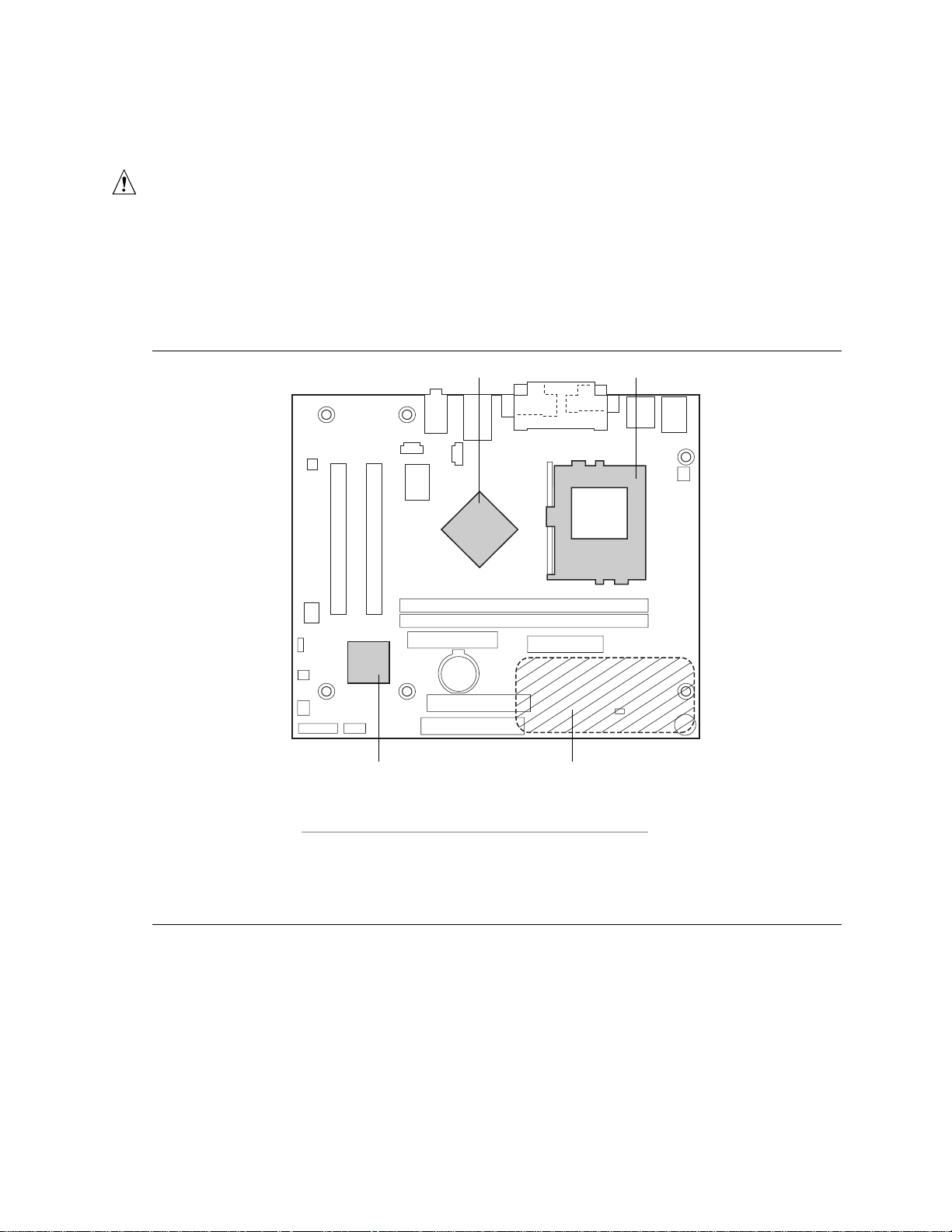
Technical Reference
2.12 Thermal Considerations
CAUTION
An ambient temperature that exceeds the board’s maximum operating temperature by 5 ºC to 10 ºC
could cause components to exceed their maximum case temperature and malfunction. For
information about the maximum operating temperature, see the environmental specifications in
Section 2.14.
Figure 12 shows the localized high-temperature zones.
A B
D C
Item Description
A Intel 82810E GMCH
B Processor
C Processor voltage regulator area
D Intel 82801BA ICH2
Figure 12. High Temperature Zones
OM11028
67
Page 68

Intel Desktop Board D810E2CB Technical Product Specification
Table 45 provides maximum component case temperatures for D810E2CB board components that
couldbe sensitive to thermal changes. Case temperatures could be affected by the operating
temperature, current load, or operatingfrequency. Maximum case temperatures are important when
considering proper airflow to cool the D810E2CB board.
Table 45. Thermal Considerations for Components
Component Maximum Case Temperature
Intel Pentium III processor
Intel Celeron processor
Intel 82810E GMCH 70oC (under bias)
Intel 82801BA ICH2 109oC (under bias)
For processor case temperature, see processor
datasheets and processor specification updates
CAUTION
The voltage regulator area can reach a temperature of up to 85 ºC in an open chassis. Ensure that
there is proper airflow to this area of the board. Failure to do so may result in damage to the
voltage regulator circuit. System integrators should ensure that proper airflow is maintained in
the voltage regulator circuit (item C in Figure 12). Components i n this area could be damaged
without adequate airflow.
2.13 Reliability
The mean time between failures (MTBF) prediction is calculated using component and subassembly
random failure rates. The calculation is based on the Bellcore Reliability Prediction Procedure, TRNWT-000332, Issue 4, September 1991. The MTBF prediction is used to estimate repair rates and
spare parts requirements.
The Mean Time Between Failures (MTBF) data is calculated from predicted data at 55 ºC.
D810E2CB board MTBF: 180193.17 hours
68
Page 69

2.14 Environmental
Table 46 lists the environmental specifications for the D810E2CB board.
Table 46. Environmental Specifications
Parameter Specification
Temperature
Non-Operating
Operating
Shock
Unpackaged 30 g trapezoidal waveform
Packaged Half sine 2 millisecond
Vibration
Unpackaged 5 Hz to 20 Hz: 0.01 g² Hz sloping up to 0.02 g² Hz
Packaged 10 Hz to 40 Hz: 0.015 g² Hz (flat)
-40 °Cto+70°C
0 °Cto+55°C
Velocity change of 170 inches/second
Product Weight (pounds) Free Fall (inches) Velocity Change (inches/sec)
<20 36 167
21-40 30 152
41-80 24 136
81-100 18 118
20 Hz to 500 Hz: 0.02 g² Hz (flat)
40 Hz to 500 Hz: 0.015 g² Hz sloping down to 0.00015 g² Hz
Technical Reference
69
Page 70

Intel Desktop Board D810E2CB Technical Product Specification
2.15 Regulatory Compliance
This section describes the D810E2CB board’s compliance with U.S. and international safety and
electromagnetic compatibility (EMC) regulations.
2.15.1 Safety Regulations
Table 47 lists the safety regulations the D810E2CB board complies with when correctly installed in
a compatible host system.
Table 47. Safety Regulations
Regulation Title
rd
UL 1950/CSA C22.2 No. 950, 3
edition
EN 60950, 2ndEdition, 1992
(with Amendments 1, 2, 3, and
4)
IEC 60950, 2ndEdition, 1991
(with Amendments 1, 2, 3, and
4)
EMKO-TSE (74-SEC) 207/94 Summary of Nordic deviations to EN 60950. (Norway, Sweden,
Bi-National Standard for Safety of Information Technology Equipment
including Electrical Business Equipment. (USA and Canada)
The Standard for Safety of Information Technology Equipment
including Electrical Business Equipment. (European Union)
The Standard for Safety of Information Technology Equipment
including Electrical Business Equipment. (International)
Denmark, and Finland)
2.15.2 EMC Regulations
Table 48 lists the EMC regulations the D810E2CB board complies with when correctly installed in a
compatible host system.
Table 48. EMC Regulations
Regulation Title
FCC (Class B) Title 47 of the Code of Federal Regulations, Parts 2 and 15, Subpart B,
Radiofrequency Devices. (USA)
ICES-003 (Class B) Interference-Causing Equipment Standard, Digital Apparatus (Canada)
EN55022: 1994 (Class B) Limits and methods of measurement of Radio Interference
Characteristics of Information Technology Equipment. (European
Union)
EN55024: 1998 Information Technology Equipment – Immunity Characteristics Limits
and methods of measurement. (European Union)
AS/NZS 3548 (Class B) Australian Communications Authority, Standard for Electromagnetic
Compatibility. (Australia and New Zealand)
CISPR 22, 2ndEdition (Class B) Limits and methods of measurement of Radio Disturbance
Characteristics of Information Technology Equipment. (International)
CISPR 24: 1997 Information Technology Equipment – Immunity Characteristics –
Limits and Methods of Measurements. (International)
70
Page 71

Technical Reference
2.15.3 Product Certification Markings (Board Level)
The D810E2CB desktop board has the following product certification markings:
• UL joint US/Canada Recognized Component mark: Consists of small c followed by a stylized
backward UR and followed by a small US. Includes adjacent UL file number for Intel desktop
boards: E210882 (component side).
• FCC Declaration of Conformity logo mark for Class B equipment; to include Intel name and
D810E2CB model designation (solder side).
• CE mark: Declaringcompliance to European Union (EU) EMC directive(89/336/EEC) and
Low Voltage directive (73/23/EEC) (component side). The CE mark should also be on the
shipping container.
• Australian Communications Authority (ACA) C-Tick mark: consists of a stylized C overlaid
with a check (tick) mark (component side), followed by Intel supplier codenumber, N-232. The
C-tick mark should also be on the shipping container.
• Printed wiring board manufacturer’s recognition mark: consists of a unique UL recognized
manufacturer’s logo, along with a flammability rating (94V-0) (solder side).
• PB part number: Intel bare circuit board part number (solder side) A37815-001. Also includes
SKU number starting with AA followed by additional alphanumeric characters.
• Battery “+ Side Up” marking: located on the component side of the board in close proximity to
the battery holder.
71
Page 72

Intel Desktop Board D810E2CB Technical Product Specification
72
Page 73

3 Overview of BIOS Features
What This Chapter Contains
3.1 Introduction................................................................................................................73
3.2 BIOS Flash Memory Organization..............................................................................73
3.3 Resource Configuration.............................................................................................74
3.4 System Management BIOS (SMBIOS).......................................................................75
3.5 USB Legacy Support .................................................................................................75
3.6 BIOS Updates............................................................................................................76
3.7 Recovering BIOS Data...............................................................................................77
3.8 Boot Options..............................................................................................................78
3.9 Fast Booting Systems with Intel
3.10 BIOS Security Features .............................................................................................80
3.1 Introduction
The D810E2CB board uses an Intel/AMI BIOS, which is stored in flash memory and can be
upgraded. In addition to the BIOS, the flash memory contains the BIOS Setup program, POST, the
PCI auto-configuration utility, and Plug and Play support.
®
Rapid BIOS Boot...................................................78
This D810E2CB board supports system BIOS shadowing, allowing the BIOS t o execute from 64-bit
onboard write-protected DRAM.
The BIOS displays a message during POST identifying the type of BIOS and a revision code. The
initial production BIOS is identified as CB81010A.86A.
For information about Refer to
The board’s compliance level with Plug and Play Table 3, page 16
3.2 BIOS Flash Memory Organization
The SST 49LF004A Firmware Hub (FWH) includes a 4 Mbit (512 KB) symmetrical flash memory
device. Internally, the device is grouped into eight 64-KB blocks that are individually erasable,
lockable, and unlockable.
73
Page 74

Intel Desktop Board D810E2CB Technical Product Specification
3.3 Resource Configuration
3.3.1 PCI Autoconfiguration
The BIOS can automatically configure PCI devices. PCI devices may be onboard or add-in cards.
Autoconfiguration lets a user insert or remove PCI cards without having to configure the system.
When a user turns on the system after adding a PCI card, the BIOS automatically configures
interrupts, the I/O space, and other systemresources. Any interrupts set to Available in Setup are
considered to be available for use by the add-in card. Autoconfiguration information is stored in
ESCD format.
For information a bout the versions of PCI and Plug and Play supported by the BIOS, see
Section 1.3.
3.3.2 PCI IDE Support
If you select Auto in the BIOS Setup program, the BIOS automatically sets up the two
PCI IDE connectors with independent I/O channel support. The IDE interface supports hard drives
up to Ultra ATA-100 and recognizes any ATAPI compliant devices, including CD-ROM drives, tape
drives, and Ultra DMA drives (see Section 1.3 for the supported version of ATAPI). The BIOS
determines the capabilities of each drive and configures them to optimize capacity and performance.
To take advantage of the high capacities typically available today, hard drives are automatically
configured for Logical Block Addressing (LBA) and to PIO Mode 3 or 4, depending on the
capability of the drive. You can override the auto-configuration options by specifying manual
configuration in the BIOS Setup program.
To use Ultra ATA-66/100 features the following items are required:
• An Ultra ATA-66/100 peripheral device
• An Ultra ATA-66/100 compatible cable
• Ultra ATA-66/100 operatingsystemdevice drivers
NOTE
✏
Ultra ATA-66/100 compatible cables are backward compatible with drives using slower IDE
transfer protocols. If an Ultra ATA-66/100 disk drive and a disk drive using any other IDE
transfer protocol are attached to the same cable, the maximum transfer rate between the drives is
reduced to that of the slowest device.
NOTE
✏
Do not connect an ATA device as a slave on the same IDE cable as an ATAPI master device. For
example, do not connect an ATA hard drive as a slave to an ATAPI CD-ROM drive.
74
Page 75

Overview of BIOS Features
3.4 System Management BIOS (SMBIOS)
SMBIOS is a Desktop Management Interface (DMI) compliant method for managing computers in a
managed network.
The main component of SMBIOS is the management information format (MIF) database, which
contains information about the computing system and its components. Using SMBIOS, a system
administrator can obtain the system types, capabilities, operational status, and installation dates for
system components. The MIF database defines the data and provides the method for accessing this
®
information. The BIOS enables applications such as Intel
SMBIOS. The BIOS stores and reports the following SMBIOS information:
• BIOS data, such as the BIOS revision level
• Fixed-system data, such as peripherals, serial numbers, and asset tags
• Resource data, such as memory size, cache size, and processor speed
• Dynamic data, such as event detection and error logging
Non-Plug and Play operating systems, such as Windows NT
obtaining the SMBIOS information. The BIOS supports an SMBIOS table interface for such
operating systems. Usingthis support, an SMBIOS service-level application running on a nonPlugandPlayoperatingsystemcanobtaintheSMBIOSinformation.
For information about
The board’s compliance level with SMBIOS Table 3, page 16
LANDesk®Client Manager to use
†
4.0, require an additional interface for
Refer to
3.5 USB Legacy Support
USB legacy support enables USB devices such as keyboards, mice, and hubs to be used even when
the operating system’s USB drivers are not yet available. USB legacysupport is used to access the
BIOS Setup program, and to install an operating system that supports USB. By default, USB legacy
support is set t o Enabled.
USB legacy support operates as follows:
1. When you apply power to the computer, legacy support is disabled.
2. POST begins.
3. USB legacy support is enabled by the BIOS allowing you to use a USB keyboard to enter and
configure the BIOS Setup program and the maintenance menu.
4. POST completes.
5. The operating system loads. While the operating system is loading, USB keyboards and mice are
recognized and may be used to configure the operating system. (Keyboards and mice are not
recognized during this period if USB legacy support was set to Disabled in the BIOS Setup
program.)
6. After the operating system loads the USB drivers, all legacy and non-legacy USB devices are
recognized by the operating system, and USB legacy support fr om the BIOS is no longer used.
To install an operating system that supports USB, verify that USB Legacy support in the BIOS
Setup program is set to Enabled and follow the operating system’s installation instructions.
NOTE
✏
USB legacy support is for keyboards, mice, and hubs only. Other USB devices are not supported
in legacy mode.
75
Page 76

Intel Desktop Board D810E2CB Technical Product Specification
3.6 BIOS Updates
The BIOS can be updated using either of the following utilities, which are available on the Intel
World Wide Web site:
• Intel
• Intel
Both utilities support the following BIOS maintenance functions:
• Verifying that the updated BIOS matches the target system to prevent accidentally installing an
• Updating both the BIOS boot block and the main BIOS. This process is fault tolerant to prevent
• Updating the BIOS boot block separately.
• Changing the language section of the BIOS.
• Updating replaceable BIOS modules, such as the video BIOS module.
• Insertinga customsplash screen.
®
Express BIOS Update utility, which enables automated updating while in the Windows
environment. Using this utility, the BIOS can be updated from a file on a hard disk, a 1.44 MB
diskette, or a CD-ROM, or from the file location on the Web.
®
Flash Memory Update Utility, which requires creation of a boot diskette and manual
rebooting of the system. Using this utility, the BIOS can be updated from a file on a 1.44 MB
diskette (from a legacy diskette drive or an LS-120 diskette drive) or a CD-ROM.
incompatible BIOS.
boot block corruption.
NOTE
✏
Review the instructions distributed with the upgrade utility before attempting a BIOS update.
For information about Refer to
The Intel World Wide Web site Section 1.2, page 16
3.6.1 Language Support
The BIOS Setup program and help messages are supported in five languages: US English, German,
Italian, French, and Spanish. The default language is US English, which is present unless another
language is selected in the BIOS Setup program.
3.6.2 Custom Splash Screen
During POST, an Intel splash screen is displayed by default. This splash screen can be replaced
with a custom splash screen. A utility is available from Intel to assist with creating a custom splash
screen. The custom splash screen can be programmed into the flash memory using the BIOS
upgrade utility. Information about this capability is available on the Intel Support World Wide Web
site.
For information about Refer to
The Intel World Wide Web site Section 1.2, page 16
76
Page 77

Overview of BIOS Features
3.7 Recovering BIOS Data
Some types of failure can destroy the BIOS. For example, the data can be lost if a power outage
occurs while the BIOS is being updated in flash memory. The BIOS can be recovered from either a
1.44 MB diskette (for recovery from an LS-120 diskette drive configured as an ATAPI removable
IDE device), or from a CD-ROM using the BIOS recovery mode. When recovering the BIOS be
aware of the following:
• Because of the small amount of code available in the nonerasable boot block area, there is no
video support. You can monitor this procedure by listening to the speaker or looking at the
recovery drive LED.
• Two beeps and the end of activity in the recovery drive indicate successful BIOS recovery.
• A series of continuous beeps indicates a failed BIOS recovery. In case of a BIOS recovery
failure, verify that SPD memory is installed and retry the BIOS recovery procedure. If non-SPD
memory is installed, replace with SPD memory and try the procedure again.
NOTE
✏
BIOS recovery cannot be accomplished if non-SPD DIMMs are installed. The SPD data structure
is required for the recovery process.
To create a BIOS recovery diskette or CD-ROM, a bootable LS-120 diskette or CD-ROM must be
created and the BIOS update files copied to it. BIOS upgrades and the Intel Flash Memory Upgrade
Utility are available from Intel Customer Support through the Intel World WideWeb site.
NOTE
✏
If the computer is configured to boot from an LS-120 diskette (in the Removable Devices submenu),
the BIOS recovery diskette must be a standard 1.44 MB diskette not a 120 MB diskette.
For information about Refer to
The BIOS recovery mode Section 2.9, page 61
The Boot menu in the BIOS Setup program Section 4.7, page 98
Contacting Intel customer support Section 1.2, page 16
77
Page 78

Intel Desktop Board D810E2CB Technical Product Specification
3.8 Boot Options
In the BIOS Setup program, the user can choose to boot from a diskette drive, hard drives,
CD-ROM, or the network. The default setting is for the diskette drive to be the first boot device, the
hard drive second, and the ATAPI CD-ROM third. The fourth device is disabled.
3.8.1 CD-ROM and Network Boot
Booting from CD-ROM is supported in compliance to the El Torito bootable CD-ROM format
specification. Under the Boot menu in the BIOS Setup program, ATAPI CD-ROM is listed as a
boot device. Boot devices are defined in priority order. Accordingly, if there is not a bootable CD in
the CD-ROM drive, the system will attempt to boot to the next defined drive.
The network can be selected as a boot device. This selection allows booting from the onboard LAN
or a network add-in card with a remote boot ROM installed.
For information about Refer to
The El Torito specification Section 1.3, page 16
3.8.2 Booting Without Attached Devices
For use in embedded applications, the BIOS has been designed so that after passing the POST, the
operating system loader is invoked even if the following devices are not present:
• Video adapter
• Keyboard
• Mouse
3.9 Fast Booting Systems with Intel®Rapid BIOS Boot
Three factors affect system boot speed:
• Selecting and configuring peripherals properly
• Using an optimized BIOS, such as the Intel
• Selecting a compatible operating system
3.9.1 Peripheral Selection and Configuration
The following techniques help improve system boot speed:
• Choose a hard drive with parameters such as “power-up to data ready” less than eight seconds,
that minimize hard drive startup delays.
• Select a CD-ROM drive with a fast initialization rate. This rate can influence POST execution
time.
• Eliminate unnecessary add-in adapter features, such as logo displays, screen repaints, or mode
changes in POST. These features may add time to the boot process.
• Try different monitors. Some monitors initialize and communicate with the BIOS more quickly,
which enables the system to boot more quickly.
®
Rapid BIOS
78
Page 79

Overview of BIOS Features
3.9.2 Intel Rapid BIOS Boot
Use of the following BIOS Setup program settings reduces the POST execution time.
In the Boot Menu:
• Set the hard disk drive as the first boot device. As a result, the POST does not first seek a
diskette drive, which saves about one second from the POST execution time.
• Disable Quiet Boot, which eliminates display of the logo splash screen. This could save several
seconds of painting complex graphic images and changing video modes.
• Enabled Intel Rapid BIOS Boot. This feature bypasses memory count and the search for a
diskette drive
In the Peripheral Configuration submenu, disable the LAN device if it will not be used. This can
reduce up to four seconds of option ROM boot time.
NOTE
✏
It is possible to optimize the boot process to the point where the system boots so quickly that the
Intel logo screen (or a custom logo splash screen) will not be seen. Monitors and hard disk drives
with minimum initialization times can also contribute to a boot time that might be so fast that
necessary logo screens and POST messages cannot be seen.
This boot time may be so fast that some drives might be not be initialized at all. If this condition
should occur, it is possible to introduce a programmable delay ranging from 3 to 30 seconds
(using the Hard Disk Pre-Delay feature of the Advanced Menu in the IDE Configuration Submenu
of the BIOS Setup Program).
For information about Refer to
IDE Configuration Submenu in the BIOS Setup Program Section 4.4.4, page 90
3.9.3 Operating System
The Microsoft Windows Millennium Edition (Windows Me) operating system has built-in
capabilities for making PCs boot more quickly. To speed operating system availability at boot time,
limit the number of applications that load into the system tray or the task bar.
79
Page 80

Intel Desktop Board D810E2CB Technical Product Specification
3.10 BIOS Security Features
The BIOS includes security features that restrict access to the BIOS Setup program and who can
boot the computer. A supervisor password and a user password can be set for the BIOS Setup
program and for booting the computer, with the following restrictions:
• The supervisor password gives unrestricted access to view and change all the Setup options in
the BIOS Setup program. This is supervisor mode.
• The user password gives restricted access to view and change Setup options in the BIOS Setup
program. This is user mode.
• If only the supervisor password is set, pressing the <Enter> key at the password prompt of the
BIOS Setup program allows the user restricted access to Setup.
• If both the supervisor and user passwords are set, users can enter either the supervisor password
or the user password to access Setup. Users have access to Setup respective to which password
is entered.
• Setting the user password restricts who can boot the computer. The password prompt will be
displayed before the computer is booted. If only the supervisor password is set, the computer
boots without asking for a password. If both passwords are set, the user can enter either
password to boot the computer.
Table 49 shows the effects of setting the supervisor password and user password. This table is for
reference only and is not displayed on the screen.
Table 49. Supervisor and User Password Functions
Supervisor
Password Set
Neither Can change all
Supervisor
only
User only N/A Can change all
Supervisor
and user set
* If no password is set, any user can change all Setup options.
For information about Refer to
Setting user and supervisor passwords Section 4.5, page 96
Mode User Mode Setup Options
options *
Can change all
options
Can change all
options
Can change all
options *
Can change a
limited number
of options
options
Can change a
limited number
of options
None None None
Supervisor Password Supervisor None
Enter Password
Clear User Password
Supervisor Password
Enter Password
Password to
Enter Setup
User User
Supervisor or
user
Password
During Boot
Supervisor or
user
80
Page 81

4 BIOS Setup Program
What This Chapter Contains
4.1 Introduction................................................................................................................81
4.2 Maintenance Menu ....................................................................................................82
4.3 Main Menu.................................................................................................................84
4.4 Advanced Menu.........................................................................................................85
4.5 Security Menu............................................................................................................96
4.6 Power Menu...............................................................................................................97
4.7 Boot Menu .................................................................................................................98
4.8 Exit Menu.................................................................................................................100
4.1 Introduction
The BIOS Setup program can be used to view and change the BIOS settings for the computer. The
BIOS Setup programis accessed by pressing the <F2> key after the Power-On Self-Test (POST)
memory test begins and before the operating system boot begins. The menu bar is shown below.
Maintenance Main Advanced Security Power Boot Exit
Table 50 lists the BIOS Setup program menu functions.
Table 50. BIOS Setup Program Menu Functions
Maintenance Main Advanced Security Power Boot Exit
✏
Clears
passwords and
allowsmemory
settings
NOTE
Allocates
resources for
hardware
components
Configures
advanced
features
available
through the
chipset
Sets
passwords
and security
features
Configures
power
management
features
Selects boot
options and
power supply
controls
In this chapter, all examples of the BIOS Setup Program menu bar include the maintenance menu;
however, the maintenance menu is displayed only when the board is in configuration mode. Section
2.9 on page 61 tells how to put the board in configuration mode.
Saves or
discards
changes to
Setup
program
options
81
Page 82
Intel Desktop Board D810E2CB Technical Product Specification
Table 51 lists the function keys available for menu screens.
Table 51. BIOS Setup Program Function Keys
BIOS Setup Program Function Key Description
<←>or<→>
<↑>or<↓>
<Tab> Selects a field
<Enter> Executes command or selects a submenu
<F9> Load the default configuration values for the current menu
<F10> Save the current values and exits the BIOS Setup program
<Esc> Exits the menu
Selects a different menu screen
Selects an item
4.2 Maintenance Menu
To access this menu, select Maintenance on the menu bar at the top of the screen.
Maintenance Main Advanced Security Power Boot Exit
Extended Configuration
The menu shown in Table 52 is for clearing Setup passwords and enabling extended configuration
mode. Setup only displays this menu in configuration mode. See Section 2.9 on page 61 for
configuration mode setting information.
Table 52. Maintenance Menu
Feature Options Description
Clear All Passwords
Clear BIS Credentials
Extended Configuration
CPU Information:
CPU Microcode Update
Revision
CPU Stepping Signature No options Displays CPU’s Stepping Signature.
• Yes (default)
• No
• Yes (default)
• No
• Default (default)
• User-Defined
No options Displays CPU’s Microcode Update Revision.
Selecting
Selecting
Service) credentials.
Selecting
configuration.
Yes
clears all passwords.
Yes
clears the WfM BIS (Boot Integrity
User-Defined
allowssetting memory
82
Page 83

BIOS Setup Program
4.2.1 Extended Configuration Submenu
To access this menu, select Maintenance on the menu bar, then Extended Configuration.
Maintenance Main Advanced Security Power Boot Exit
Extended Configuration
The submenu shown in Table 53 is for setting system memory configuration. This submenu
becomes available when User-Defined is selected under Extended Configuration.
CAUTION
Choosing the wrong settings could cause system problems. Do not change these settings unless
you have all the necessary information about the installed memory.
Table 53. Extended Configuration Submenu
Feature Options Description
Extended Configuration Default (default)
User-Defined
Memory Control:
SDRAM Auto
Configuration
CAS# Latency
SDRAM RAS# to CAS#
delay
SDRAM RAS#
Precharge
• Auto (default)
• User-Defined
• 3
• 2
• Auto (default)
• 3
• 2
• Auto (default)
• 3
• 2
• Auto (default)
Selecting user-defined allows you to select
Defined
items listed under Memory Control below.
Note: If
in the Advanced Menu as: “Extended Menu: Used.”
Sets extended memory configuration options to auto or
user-defined.
Selects the number of clock cycles required to address a
column in memory.
Selects the number of clock cycles between addressing a
row and addressing a column.
Selects the length of time required before accessing a
new row.
. Selecting
User-Defined
User-Defined
is selected, the status will be displayed
allows you to configure the
DefaultorUser-
83
Page 84

Intel Desktop Board D810E2CB Technical Product Specification
4.3 Main Menu
To access this menu, select Main on the menu bar at the top of the screen.
Maintenance Main Advanced Security Power Boot Exit
Table54 describes the Main Menu. This menu reports processor and memory information and is for
configuring the system date and system time.
Table 54. Main Menu
Feature Options Description
BIOS Version No options Displays the version of the BIOS
Processor Type No options Displays processor type
Processor Speed No options Displays processor speed
Front Side Bus
Speed
Cache RAM No options Displays the size of second-level cache
Total Memory No options Displays the total installed SDRAM memory
Memory Bank 0
Memory Bank 1
Language
System Time Hour, minute, and
System Date Month, day, and year Specifies the current date
No options Displays the system bus speed
No options
No options
• English (default)
• Français
• Portugues
•
second
Displays
or absence of memory in Memory Banks 0 and 1
Selects the current default language used by the BIOS
Specifies the current time
SDRAMorNot Installed
indicating the presence
84
Page 85

BIOS Setup Program
4.4 A dvanced Menu
To access this menu, select Advanced on the menu bar at the top of the screen.
Maintenance Main Advanced Security Power Boot Exit
PCI Configuration
Boot Configuration
Peripheral Configuration
IDE Configuration
Diskette Configuration
Event Log Configuration
Video Configuration
Table 55 describes the Advanced Menu. This menu is used for setting advanced features that are
available through the chipset.
Table 55. Advanced Menu
Feature Options Description
Extended Configuration No options If
PCI Configuration Select to display
submenu
Boot Configuration Select to display
submenu
Peripheral Configuration Select to display
submenu
IDE Configuration Select to display
submenu
Diskette Configuration Select to display
submenu
Event Log Configuration Select to display
submenu
Video Configuration Select to display
submenu
Used
is displayed,
Extended Configuration under the Maintenance Menu.
Configures individual PCI slot’s IRQ priority. When
selected, displays the PCI Configuration submenu.
Configures Plug and Play and the Numlock key, and
resets configuration data. When selected, displays the
Boot Configuration submenu.
Configures peripheral ports and devices. When selected,
displays the Peripheral Configuration submenu.
Specifies type of connected IDE devices.
When selected, displays the Diskette Configuration
submenu.
Configures Event Logging. When selected, displays the
Event Log Configuration submenu.
Configures video features. When selected, displays the
Video Configuration submenu.
User-Defined
has been selected in
85
Page 86

Intel Desktop Board D810E2CB Technical Product Specification
4.4.1 PCI Configuration Submenu
To access this submenu, select Advanced on the menu bar, then PCI Configuration.
Maintenance Main Advanced Security Power Boot Exit
PCI Configuration
Boot Configuration
Peripheral Configuration
IDE Configuration
Diskette Configuration
Event Log Configuration
Video Configuration
The submenu represented by Table 56 is for configuring the IRQ priority of PCI slots individually.
Table 56. PCI Configuration Submenu
Feature Options Description
PCISlot1IRQPriority
PCISlot2IRQPriority
• Auto (default)
3
5
9
10
11
• Auto (default)
3
5
9
10
11
Allowsselection of IRQ priority.
Allowsselection of IRQ priority.
86
Page 87

BIOS Setup Program
4.4.2 Boot Configuration Submenu
To access this submenu, select Advanced on the menu bar, then Boot Configuration.
Maintenance Main Advanced Security Power Boot Exit
PCI Configuration
Boot Configuration
Peripheral Configuration
IDE Configuration
Diskette Configuration
Event Log Configuration
Video Configuration
The submenu represented by Table 57 is for setting Plug and Play options, resetting configuration
data, and the power-on state of the Numlock key.
Table 57. Boot Configuration Submenu
Feature Options Description
Plug & Play O/S
Reset Config Data
Numlock
• No (default)
• Yes
• No (default)
• Yes
• Off
• On (default)
Specifies if manual configuration is desired.
No
lets the BIOS configureall devices. This setting is
appropriate when using a Plug and Play operating system.
Yes
lets the operating system configure Plug and Play
devices not required to boot the system. This option is
available for use during lab testing.
No
does not clear the PCI/PnP configuration data stored in
flash memory on the next boot.
Yes
clears the PCI/PnP configuration data stored in flash
memory on the next boot.
Specifies the power-on state of the Numlock feature on the
numeric keypad of the keyboard.
87
Page 88

Intel Desktop Board D810E2CB Technical Product Specification
4.4.3 Peripheral Configuration Submenu
To access this submenu, select Advanced on the menu bar, then Peripheral Configuration.
Maintenance Main Advanced Security Power Boot Exit
PCI Configuration
Boot Configuration
Peripheral Configuration
IDE Configuration
Diskette Configuration
Event Log Configuration
Video Configuration
The submenu represented in Table 58 is used for configuring computer peripherals.
Table 58. Peripheral Configuration Submenu
Feature Options Description
Serial port A
Base I/O address
(This feature is present
only when Serial Port A
is set to
Interrupt
(This feature is present
only when Serial Port A
is set to
Parallel port
Mode
Enabled
Enabled
)
)
• Disabled
• Enabled
• Auto (default)
• 3F8 (default)
• 2F8
• 3E8
• 2E8
• IRQ 3
• IRQ 4
(default)
• Disabled
• Enabled
• Auto (default)
• Output Only
• Bi-directional
(default)
• EPP
• ECP
Configures serial port A.
Auto
assigns the first free COM port, normally COM1, the
address 3F8h, and the interrupt IRQ4.
An * (asterisk) displayed next to an address indicates a
conflict with another device.
Specifies the base I/O address for serial port A, if serial port
A is Enabled.
Specifies the interrupt for serial port A, if serial port A is
Enabled.
Configures the parallel port.
Auto
assigns LPT1 the address 378h and the interrupt IRQ7.
An * (asterisk) displayed next to an address indicates a
conflict with another device.
Selects the mode for the parallel port. Not available if the
parallel port is disabled.
Output Only
Bi-directi onal
EPP
is Extended Parallel Port mode, a high-speed
bi-directional mode.
ECP
directional mode.
operates in AT†-compatible mode.
operates in PS/2-compatible mode.
is Enhanced Capabilities Port mode, a high-speed bi-
continued
88
Page 89

Table 58. Peripheral Configuration Submenu (continued)
Feature Options Description
Base I/O address
(This feature is present
only when Parallel Port
is set to
Interrupt
(This feature is present
only when Parallel Port
is set to
DMA
(This feature is present
only when Parallel Port
Mode is set to
Audio Device
LAN Device
Legacy USB Support
Enabled
Enabled
)
)
ECP
)
• 378 (default)
• 278
• IRQ 5
• IRQ 7
(default)
• 1
• 3 (default)
• Disabled
• Enabled
(default)
• Disabled
• Enabled
(default)
• Disabled
• Enabled
(default)
Specifies the base I/O address for the parallel port.
Specifies the interrupt for the parallel port.
Specifies the DMA channel.
Enables or disables the onboard audio subsystem.
Enables or disables the LAN device.
Enables or disables USB legacy support.
(See Section 3.5 on page 75 for more information.)
BIOS Setup Program
89
Page 90

Intel Desktop Board D810E2CB Technical Product Specification
4.4.4 IDE Configuration Submenu
To access this submenu, select Advanced on the menu bar, then IDE Configuration.
Maintenance Main Advanced Security Power Boot Exit
PCI Configuration
Boot Configuration
Peripheral Configuration
IDE Configuration
Diskette Configuration
Event Log Configuration
Video Configuration
The menu represented in Table 59 is used to configure IDE device options.
Table 59. IDE Configuration Submenu
Feature Options Description
IDE Controller
Hard Disk Pre-Delay
Primary IDE Master Select to display sub-
Primary IDE Slave Select to display sub-
Secondary IDE Master Select to display sub-
Secondary IDE Slave Select to display sub-
• Disabled
• Primary
• Secondary
• Both (default)
• Disabled (default)
• 3 Seconds
• 6 Seconds
• 9 Seconds
• 12 Seconds
• 15 Seconds
• 21 Seconds
• 30 Seconds
menu
menu
menu
menu
Specifies the integrated IDE controller.
Primary
Secondary
Both
Specifies the hard disk drive pre-delay.
Reports type of connected IDE device. When selected,
displays the Primary IDE Master submenu.
Reports type of connected IDE device. When selected,
displays the Primary IDE Slave submenu.
Reports type of connected IDE device. When selected,
displays the Secondary IDE Master submenu.
Reports type of connected IDE device. When selected,
displays the Secondary IDE Slave submenu.
enables only the primary IDE controller.
enables only the secondary IDE controller.
enables both IDE controllers.
90
Page 91

BIOS Setup Program
4.4.4.1 Primary/Secondary IDE Master/Slave Submenus
To access these submenus, select Advanced on the menu bar, then IDE Configuration and then the
master or slave to be configured.
Maintenance Main Advanced Security Power Boot Exit
PCI Configuration
Boot Configuration
Peripheral Configuration
IDE Configuration
Primary IDE Master
Primary IDE Slave
Secondary IDE Master
Secondary IDE Slave
Diskette Configuration
Event Log Configuration
Video Configuration
There are four IDE submenus: primary master, primary slave, secondary master, and secondary
slave. Table 60 shows the format of the IDE submenus. For brevity, only one example is shown.
Table 60. Primary/Secondary IDE Master/Slave Submenus
Feature Options Description
DriveInstalled No options Displays the type of drive installed
Type
Maximum Capacity No options Displays the capacity of the drive.
LBA Mode Control
Multi-Sector Transfers
• None
• User
• Auto (default)
• CD-ROM
• ATAPI Removable
• Other ATAPI
• IDE Removable
• Disabled
• Enabled (default)
• Disabled (default)
• 2Sectors
• 4Sectors
• 8Sectors
• 16 Sectors
Specifies the IDE configuration mode for IDE devices.
User
allows capabilities to be changed.
Auto
fills-in capabilities from ATA/ATAPI device.
Enables or disables LBA mode control.
Specifies number of sectors per block for transfers
from the hard disk drive to memory.
Check the hard disk drive’s specifications for optimum
setting.
continued
91
Page 92

Intel Desktop Board D810E2CB Technical Product Specification
Table 60. Primary/Secondary IDE Master/Slave Submenus (continued)
Feature Options Description
PIO Mode
Ultra DMA
Cable Detected No options Displays the type of cable connected to the IDE
• Auto (default)
• 0
• 1
• 2
• 3
• 4
• Disabled (default)
• Mode 0
• Mode 1
• Mode 2
• Mode 3
• Mode 4
Specifies the PIO mode.
Specifies the Ultra DMA mode for the drive.
interface: 40-conductor or 80-conductor (for Ultra
ATA-100 devices).
92
Page 93

4.4.5 Diskette Configuration Submenu
To access this menu, select Advanced on the menu bar, then Diskette Configuration.
Maintenance Main Advanced Security Power Boot Exit
PCI Configuration
Boot Configuration
Peripheral Configuration
IDE Configuration
Diskette Configuration
Event Log Configuration
Video Configuration
The submenu represented by Table 61 is used for configuring the diskette drive.
Table 61. Diskette Configuration Submenu
Feature Options Description
Diskette Controller
Floppy A
Diskette Write-Protect
• Disabled
• Enabled (default)
• Not Installed
• 360 KB 5¼"
• 1.2 MB 5¼"
• 720 KB 3½"
• 1.44/1.25 MB 3½" (default)
• 2.88 MB 3½"
• Disabled (default)
• Enabled
Disables or enables the integrated diskette
controller.
Specifies the capacity and physical size of
diskette drive A.
Disables or enables write-protect for the
diskette drive.
BIOS Setup Program
93
Page 94

Intel Desktop Board D810E2CB Technical Product Specification
4.4.6 Event Log Configuration Submenu
To access this menu, select Advanced on the menu bar, then Event Log Configuration.
Maintenance Main Advanced Security Power Boot Exit
PCI Configuration
Boot Configuration
Peripheral Configuration
IDE Configuration
Diskette Configuration
Event Log Configuration
Video Configuration
The submenu represented by Table 62 is used to configure the event logging features.
Table 62. Event Log Configuration Submenu
Feature Options Description
Event log No options Indicates if there is space available in the event log.
Event log validity No options Indicates if the contents of the event log are valid.
View event log [Enter] Displays the event log.
Clear all event logs
Event Logging
Mark events as read [Enter] Marks all events as read.
• No (default)
• Yes
• Disabled
• Enabled (default)
Clears the event log after rebooting.
Enables logging of events.
94
Page 95

4.4.7 Video Configuration Submenu
To access this menu, select Advanced on the menu bar, then Video Configuration.
Maintenance Main Advanced Security Power Boot Exit
PCI Configuration
Boot Configuration
Peripheral Configuration
IDE Configuration
Diskette Configuration
Event Log Configuration
Video Configuration
The submenu represented in Table 63 is for configuring the video features.
Table 63. Video Configuration Submenu
Feature Options Description
Primary Video Adapter
• AGP (default)
• PCI
Selects primary video adapter to be used during
boot.
BIOS Setup Program
95
Page 96

Intel Desktop Board D810E2CB Technical Product Specification
4.5 Security Menu
To access this menu, select Security from the menu bar at the top of the screen.
Maintenance Main Advanced Security Power Boot Exit
The menu represented by Table 64 is for setting passwords and security features.
Table 64. Security Menu
Feature Options Description
Supervisor Password Is No options Reports if there is a supervisor password set.
User Password Is No options Reports if there is a user password set.
Set Supervisor Password Password can be up to seven
alphanumeric characters.
Set User Password Password can be up to seven
alphanumeric characters.
Clear User Password
(Note 1)
User Access Level
(Note 2)
Unattended Start
(Note 1)
Notes:
1. This feature appears only if a user password has been set.
2. This feature appears only if a supervisor password has been set.
• Yes (default)
• No
• Limited
• No Access
• View Only
• Full (default)
• Disabled (default)
• Enabled
Specifies the supervisor password.
Specifies the user password.
Clears the user password.
Sets BIOS Setup Utility access rights for user
level.
Enabled allows system to complete the boot
process without a password. The keyboard
remains locked until a password is entered.
A password is required to boot from a
diskette.
96
Page 97

4.6 Power Menu
To access this menu, select Power from the menu bar at the top of the screen.
Maintenance Main Advanced Security Power Boot Exit
The menu represented in Table 65 is for setting the power management features.
Table 65. Power Menu
Feature Options Description
Power Management
(Note)
Inactivity Timer
(Note)
Hard Drive
(Note)
ACPI Suspend State
Power Button Mode
Note: Power Management, Inactivity Timer, and Hard Drive features apply only for APM operating systems.
• Disabled
• Enabled (default)
• Off
• 1 Minute
• 5 Minutes
• 10 Minutes
• 20 Minutes
(default)
• 30 Minutes
• 60 Minutes
• 120 Minutes
• Disabled (default)
• Enabled
• S1 State (default)
• S3 State
• On/Off (default)
• Suspend
Enable or disable the BIOS power management feature.
Specifies the amount of time before the computer
enters standby mode, when APM power management is
active.
Enables or disables power management for hard disks
during standby and suspend modes, when APM power
management is active.
Specifies the ACPI suspend state.
Selects the operating mode for the power button.
BIOS Setup Program
97
Page 98

Intel Desktop Board D810E2CB Technical Product Specification
4.7 Boot Menu
To access this menu, select Boot from the menu bar at the top of the screen.
Maintenance Main Advanced Security Power Boot Exit
IDE Drive Configuration
The menu represented in Table 66 is used to set the boot features and the boot sequence.
Table 66. Boot Menu
Feature Options Description
Silent Boot
Intel Rapid BIOS
Boot
Scan User Flash
Area
After Power
Failure
Wake on Modem
Ring
Wake on LAN
Wake on PME
• Disabled
• Enabled (default)
• Disabled
• Enabled (default)
• Disabled (default)
• Enabled
• Stays Off
• Last State (default)
• Power On
• Stay Off (default)
• Power On
• Stay Off (default)
• Power On
• Stay Off (default)
• Power On
Disabled
Enabled
Enables the computer to boot without running certain POST
tests.
Enables the BIOS to scan the flash memory for user binary
files that are executed at boot time.
Specifies the mode of operation if an AC power loss occurs.
Stay Off
pressed.
Last State
loss occurred.
Power On
In APM mode only, specifies how the computer responds to
an incoming call on an installed modem when the power is
off.
In APM mode only, determines how the system responds to a
LAN wake up event.
In APM mode only, determines how the system responds to a
PCI power management event.
displays normal POST messages.
displays OEM graphic instead of POST messages.
keeps the power off until the power button is
restores the previous power state before power
restores power to the computer.
continued
98
Page 99

Table 66. Boot Menu (continued)
Feature Options Description
1stBoot Device
nd
Boot Device
2
rd
Boot Device
3
th
Boot Device
4
• Floppy
• ARMD-FDD
(Note 1)
• ARMD-HDD
(Note 2)
• IDE-HDD
(Note 3)
• ATAPI CDROM
• Intel UNDI,
PXE 2.0
(Note 4)
• Disabled
IDE Drive Configuration
Primary Master IDE
Primary Slave IDE
Secondary Master IDE
• 1
• 2
• 3
• 4
st
nd
rd
th
IDE (default)
IDE
IDE
IDE
Secondary Slave IDE
Notes:
1 ARMD-FDD = ATAPI removabledevice - floppydisk drive
2 ARMD-HDD = ATAPI removable device - hard disk drive
3 HDD = Hard Disk Drive
4 This boot device is availableonly when the onboard LAN subsystem is present.
Specifies the boot sequence according to the device
type. The computer will attempt to boot from up to four
devices as specified here. Only one of the devices can
be an IDE hard disk drive. To specify boot sequence:
1. Select the boot device with <↑>or<↓>.
2. Press <Enter> to set the selection as the intended
boot device.
The default settings for the first through fourth boot
devices are, respectively:
• Floppy
• IDE-HDD
• ATAPI CDROM
• Disabled
NOTE: To configure the computer to boot from an IDE
hard disk drive, set a boot device in the Setup feature to
IDE-HDD
. Determine the IDE channel, and master or
slave mode of the drive. Then, in the next Setup
feature,
mode to
1stIDE
The
IDE Drive Configuration
1stIDE
.
specifies the IDE hard disk drive to boot from.
nd
2
through
4thIDE
note above for more information.
To specify the drive to boot from:
1. Use <↑>or<↓> to select the channel, and master
or slave mode of the drive to boot from.
2. Press <Enter>.
3. Use <↑>or<↓> to select 1
4. Press <Enter> to set the selection.
BIOS Setup Program
, set that channel and
settings are ignored. See the
st
IDE.
99
Page 100

Intel Desktop Board D810E2CB Technical Product Specification
4.8 Exit Menu
Maintenance Main Advanced Security Power Boot Exit
The menu represented in Table 67 is for exiting the BIOS Setup program, saving changes, and
loading and saving defaults.
Table 67. Exit Menu
Feature Description
Exit Saving Changes Exits and saves the changes in CMOS SRAM.
Exit Discarding Changes Exits without saving any changes made in the BIOS Setup program.
Load Setup Defaults Loads the factory default values for all the Setup options.
Load Custom Defaults Loads the custom defaults for Setup options.
Save Custom Defaults Saves the current values as custom defaults. Normally, the BIOS reads the
Setup values from flash memory. If this memory is corrupted, the BIOS reads
the custom defaults. If no custom defaults are set, the BIOS reads the factory
defaults.
Discard Changes Discards changes without exiting Setup. The option values present when the
computer was turned on are used.
100
 Loading...