

Page 1
80960MC
EMBEDDED 32-BIT MICROPROCESSOR
WITH INTEGRATED FLOATING-POINT UNIT
AND MEMORY MANAGEMENT UNIT
Commercial
■ High-Performance Embedded Architecture
— 25 MIPS Burst Execution at 25 MHz
— 9.4 MIPS* Sustained Execution at
25 MHz
■ On-Chip Floating Point Unit
— Supports IEEE 754 Floating Point
Standard
— Full Transcendental Support
— Four 80-Bit Registers
— 13.6 Million Whetstones/s
(Single Precision) at 25 MHz
■ 512-Byte On-Chip Instruction Cache
— Direct Mapped
— Parallel Load/Decode for Uncached
Instructions
■ Multiple Register Sets
— Sixteen Global 32-Bit Registers
— Sixteen Local 32-Bit Registers
— Four Local Register Sets Stored
On
-Chip (Sixteen 32-Bit Registers per
Set)
— Register Scoreboarding
■ On-Chip Memory Management Unit
— 4 Gbyte Virtual Address Space per
Task
— 4 Kbyte Pages with Supervisor/User
Pro
tection
■ Built-in Interrupt Controller
— 32 Priority Levels
— 248 Vectors
— Supports M8259A
— 3.4 µs Latency @ 25 MHz
■ Easy to Use, High Bandwidth 32-Bit Bus
— 66.7 Mbytes/s Burst
— Up to 16 Bytes Transferred per Burst
■ Multitasking and Multiprocessor Support
— Automatic Task dispatching
— Prioritized Task Queues
■ Advanced Package Technology
— 132-Lead Ceramic Pin Grid Array
FOUR
80-BIT FP
REGISTERS
80-BIT
FPU
INSTRUCTION
FETCH UNIT
SIXTEEN
32-BIT GLOBAL
REGISTERS
512-BYTE
INSTRUCTION
CACHE
64- BY 32-BIT
LOCAL
REGISTER
CACHE
INSTRUCTION
DECODER
32-BIT
INSTRUCTION
EXECUTION
UNIT
MICRO-
INSTRUCTION
SEQUENCER
MMU
MICRO-
INSTRUCTION
ROM
32-BIT
BUS CONTROL
LOGIC
32-BIT
BURST
BUS
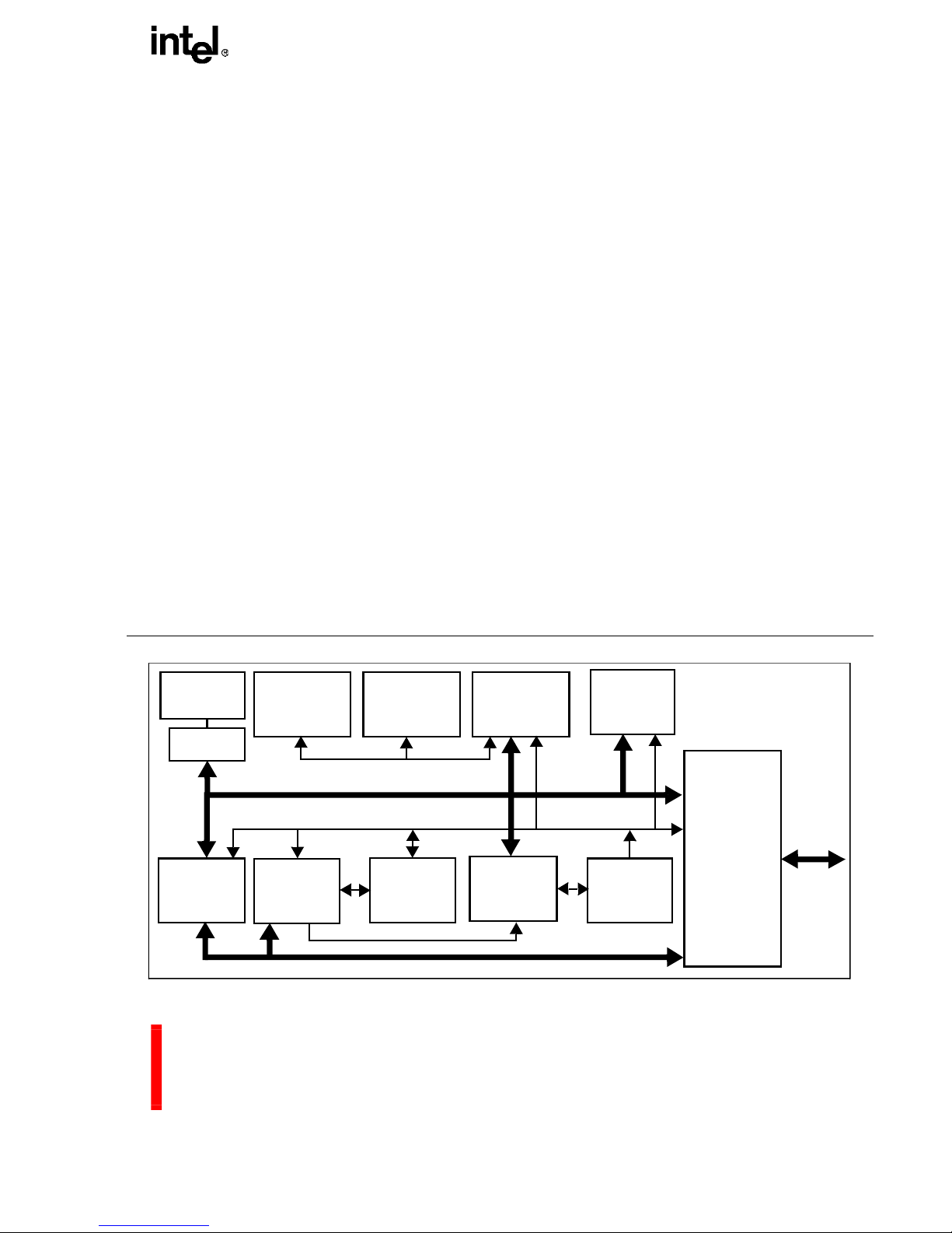
Figure 1. The 80960MC Processor’s Highly Parallel Architecture
© INTEL CORPORATION, 2004 September, 2004 Order Number: 273123-002
Page 2

Information in this document is provided in connection with Intel products. No license, express or implied, by
estopp el or otherw ise, to any intellect ual proper ty rights is granted by this documen t. Except as prov ided in
Intel’s Terms and Conditions of Sale for such products, Intel assumes no liability whatsoever, and Intel
disclaims any express or imp lied warranty , relating to sale and/or use of Intel products including lia bility or
warrant ie s relat ing to fit ne ss for a partic ular pu rpo se, me rcha ntab ility , or in fringe men t of any patent , copy right
or other intellectual property right. Intel products are not intended for use in medical, life saving, or life
sus taining applications. Intel ma y make changes to speci fications an d product descriptions at any time, without
notice. Contact your local In tel sales off ice or your dis tributor to obtain the lates t specifications and befo re
placing your product order.
Intel retains the right to make changes to specifications and product descriptions at any time, without notice.
*Third party brands and names are the property of their respective owners.
Copies of documents which have an ordering number and are referenced in this document, or other Intel
literature, may be obtained from:
Intel Corporation
P.O. Box 7641
Mt. Prospect IL 60056-7641
or call 1-800-879-4683
Many documents are available for download from Intel’s website at http://www.intel.com
Copyright © Intel Corporation 1997
Page 3

80960MC
1.0 THE i960® MC PROCESSOR ...................................................................................................................1
1.1 Key Performance Features .................................................................................................................2
1.1.1 Memory Space And Addressing Modes ................................................................................... 4
1.1.2 Data Types ............................................................................................................................... 4
1.1.3 Large Register Set ................................................................................................................... 4
1.1.4 Multiple Register Sets ..............................................................................................................5
1.1.5 Instruction Cache ..................................................................................................................... 5
1.1.6 Register Scoreboarding ...........................................................................................................5
1.1.7 Memory Management and Protection ......................................................................................6
1.1.8 Floating-Point Arithmetic ..........................................................................................................6
1.1.9 Multitasking Support ................................................................................................................7
1.1.10 Synchronization and Communication ....................................................................................7
1.1.11 High Bandwidth Local Bus .....................................................................................................7
1.1.12 Multiple Processor Support .................................................................................................... 7
1.1.13 Interrupt Handling ..................................................................................................................8
1.1.14 Debug Features .....................................................................................................................8
1.1.15 Fault Detection ....................................................................................................................... 8
1.1.16 Inter-Agent Communications (IAC) ........................................................................................9
1.1.17 Built-in Testability ................................................................................................................... 9
1.1.18 Compatibility with 80960K-Series .......................................................................................... 9
1.1.19 CHMOS .................................................................................................................................. 9
2.0 ELECTRICAL SPECIFICATIONS ........................................................................................................... 13
2.1 Power and Grounding .......................................................................................................................13
2.2 Power Decoupling Recommendations .............................................................................................13
2.3 Connection Recommendations ........................................................................................................ 13
2.4 Characte ris ti c Curv es ........ .... ........... ........... ............ ........... ............ .... ........... ............ ....... ............ ....13
2.5 Test Load Ci rcuit ........... ........... ............ ........... ............ ........... .... ........... ............ ................... ........... . 16
2.7 DC Characteristics ............................................................................................................................ 17
2.6 Absolu te Max im um Ra tin gs ... ........... ........... ............ .... ........... ............ ........... ............ ................... ... . 17
2.8 AC Specifications ............................................................................................................................. 18
2.9 Design Con side rations ............. ............ ........... ............ ........... ............ ... ............ ........... ............ .... ....22
3.0 MECHANICAL DATA ..............................................................................................................................22
3.1 Packaging .........................................................................................................................................22
3.1.1 Pin Assignment ......................................................................................................................22
3.2 Pinout ...............................................................................................................................................26
3.3 Package The rm al Spec if ic ati on ........ ........... .... ............ ........... ............ ... ............ ........... ....................28
4.0 WAVEFOR M S .......... ............ ........... .... ............ ........... .... ........... ............ ........... .... ....................... ........... . 30
5.0 REVISION HISTORY ............................................................................................................................... 35
iii
Page 4

80960MC
FIGURES
Figure 1. 80960MC Programming Environment ........................................................................................1
Figure 2. Instruction Formats ....................................................................................................................4
Figure 3. Multiple Register Sets Are Stored On-Chip ...............................................................................6
Figure 4. Connection Recommendations for Low Current Drive Network ..............................................13
Figure 5. Connection Recommendations for High Current Drive Network ..............................................13
Figure 6. Typical Supply Current vs. Case Temperature ........................................................................14
Figure 7. Typical Current vs. Frequency (Room Temp) ..........................................................................14
Figure 8. Typical Current vs. Frequency (Hot Temp) ..............................................................................15
Figure 9. Worst-Case Voltage vs. Output Current on Open-Drain Pins ..................................................15
Figure 10. Capacit iv e Dera tin g Curv e ......... .... ............ ... ............ ........... ............ .... ........... ............ .............15
Figure 11. Test Load Circuit for Three-State Output Pins .........................................................................16
Figure 12. Test Load Circuit for Open-Drain Output Pins .........................................................................16
Figure 13. Drive Levels and Timing Relationships for 80960MC Signals .................................................18
Figure 14. Timing Relationship of L-Bus Signals ......................................................................................19
Figure 15. System and Processor Clock Relationship ..............................................................................19
Figure 16. Processor Clock Pulse (CLK2) ................................................................................................21
Figure 17. RESET Signal Timing ..............................................................................................................21
Figure 18. HOLD Timing ...........................................................................................................................22
Figure 19. 132-Lead Pin-Grid Array (PGA) Package ................................................................................23
Figure 20. 80960MC PGA Pinout—View from Bottom (Pins Facing Up) ..................................................24
Figure 21. 80960MC PGA Pinout—View from Top (Pins Facing Down) ..................................................25
Figure 22. 25 MHz Maximum Allowable Ambient Temperature ................................................................29
Figure 23. Non-Burst Read and Write Transactions Without Wait States .................................................30
Figure 24. Burst Read and Write Transaction Without Wait States ..........................................................31
Figure 25. Burst Write Transaction with 2, 1, 1, 1 Wait States ..................................................................32
Figure 26. Access es Gener ated by Qu ad Word Read Bus Request, Misaligned Two By tes from
Quad Word Boundary (1, 0, 0, 0 Wait States) .........................................................................33
Figure 27. Interrupt Acknowledge Transaction .........................................................................................34
Figur e 28. Bus Exchange Tran saction (PBM = Pri mary Bus Ma ster, SBM = Secondary Bus Master) .....35
TABLES
Table 1. 80960MC Instruction Set ...........................................................................................................3
Table 2. Memory Addressing Modes .......................................................................................................4
Table 3. Sample Floating-Point Execution Times (µs) at 25 MHz ...........................................................7
Table 4. 80960MC Pin Description: L-Bus Signals ..................................................................................9
Table 5. 80960MC Pin Description: Support Signals .............................................................................11
Table 6. DC Characteristics ...................................................................................................................17
Table 7. 80960MC AC Characteristics (25 MHz) ...................................................................................20
Table 8. 80960MC PGA Pinout — In Pin Order .....................................................................................26
Table 9. 80960MC PGA Pinout — In Signal Order ................................................................................27
Table 10. 80960MC PGA Package Thermal Characteristics ...................................................................28
iv
Page 5
80960MC
1.0 THE i960® MC PROCESSOR
The 80960MC, a member of Intel’s i960® 32-bit
processor family, is ideally suited for embedded
applications. It includes a 512-byte instruction cache
and a built-in interrupt controller. The 80960MC has
a larg e registe r set, mul tiple parallel execut ion units
and a high-bandwidth burst bus. Using advanced
RISC technology, this processor is capable of
execution rates in excess of 9.4 million instructions
per s eco nd
range of applications including non-impact printers,
I/O control and specialty instrumentation. The
embedded market includes applications as diverse
as industrial automation, avionics, image
processing, graphics and networking. These types of
applications require high integration, low power
consumption, quick interrupt response times and
* Relative to Digital Equipment Corporation’s VAX-11/780*
at 1 MIPS
*
. The 8 0960 MC is we ll- suite d for a w ide
high performance. Since time to market is critical,
embedded processors must be easy to use in both
hardware and software designs.
All members of the i960 processor family share a
comm on c ore ar ch itect ure w hic h util izes RI SC te chnology so that, except for special functions, the
family members are object-code compatible. Each
new p ro ce ss o r in th e family a dds its o w n sp ec ia l set
of functions to the core to satisfy the needs of a
specific application or range of applications in the
embedded market.
The 80960MC includes an integrated Floating Point
Unit (FPU), a Memory Management Unit (MMU),
multitasking support, and multiprocessor support.
Two commercial members of the i960
®
family
provide similar features: the 80960KB processor with
integrated FPU and the 80960KA without floatingpoint.
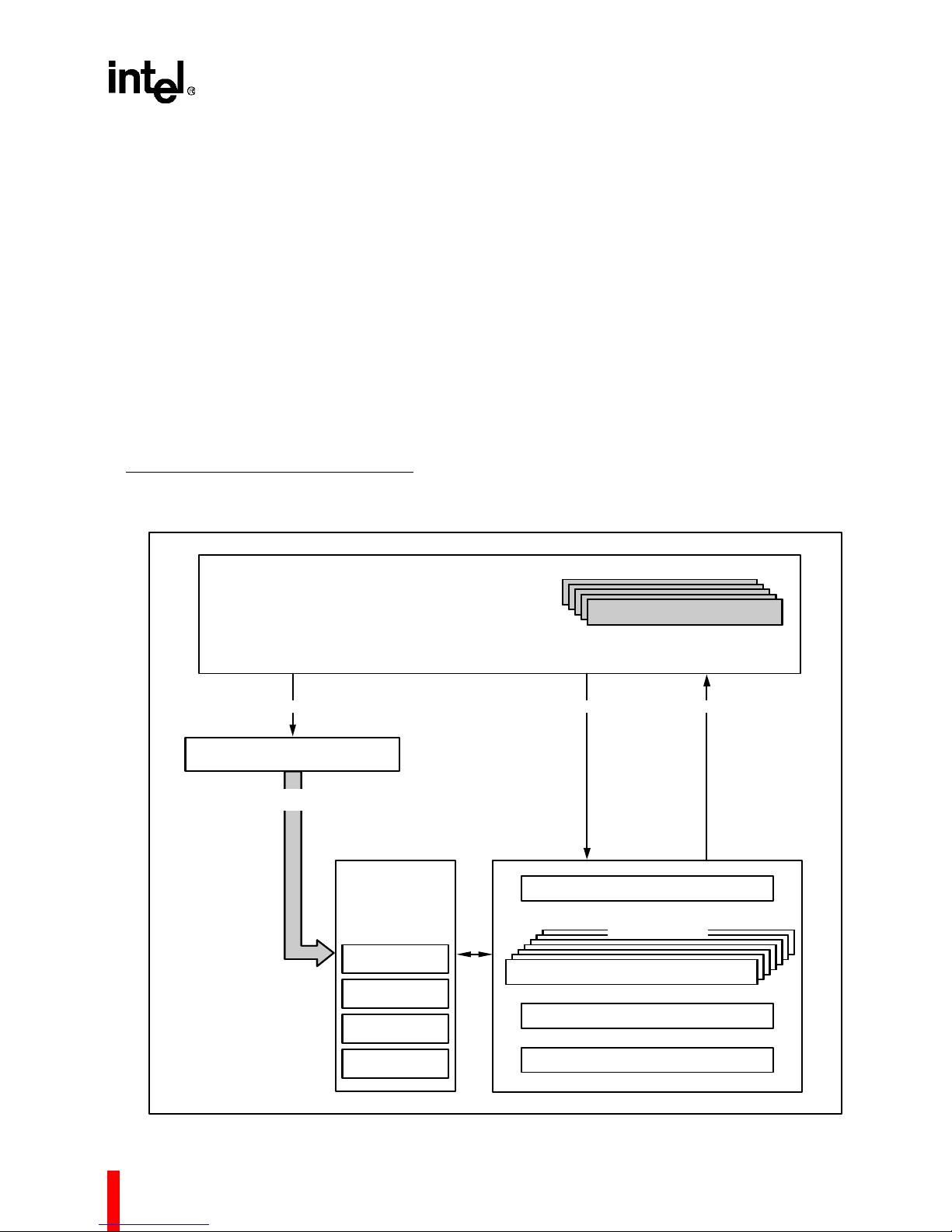
FFFF FFFFH0000 0000H
ADDRESS SPACE
ARCHITECTURALLY
DATA STRUCTURES
FETCH LOAD STORE
INSTRUCTION CACHE
INSTRUCTION
STREAM
INSTRUCTION
EXECUTION
PROCESSOR STATE
REGISTERS
INSTRUCTION
POINTER
ARITHMETIC
CONTROLS
PROCESS
CONTROLS
TRACE
CONTROLS
SIXTEEN 32-BIT GLOBAL REGISTERS
REGISTER CACHE
SIXTEEN 32-BIT LOCAL REGISTERS
FOUR 80-BIT FLOATING POINT REGISTERS
CONTROL REGISTERS
DEFINED
r15
g0
g15
r0
Figure 1. 80960MC Programming Environment
1
Page 6

80960MC
1.1 Key Performan ce Featu res
The 80 96 0 arc hitec tur e is b ased on the mos t rece nt
advances in microprocessor technology and is
grounded in Intel’s l ong exp erience in the de sign a nd
manufacture of embedded microprocessors. Many
features contribute to the 80960MC’s exceptional
performance:
1. Large Register Set. Havi ng a lar ge nu m ber of
registers reduces the number of times that a
processor needs to access memory. Modern
compilers can take advantage of this fe ature to
optimize execution speed. For maximum flexibility, the 80960MC provides thirty-two 32-bit
registers. (See Figure 2.)
2. Fast I nst ruction E xecut ion. Sim ple functi ons
make up the bulk of instructions in most
programs so that execution speed can be
improved by ensuring that these core instructions are ex ecut ed as quic kly as po ssib le. Th e
most frequently executed instructions such as
register-register moves, add/subtract, logical
operations and shifts execute in one to two
cycles. (Table 1 contains a list of instructions.)
3. Load/Store Ar chit e cture. One way to improve
execution speed is to reduce the number of
times that the processor must access memory
to perform an operation. As with other processors based on RISC technology, the 80960MC
has a Load/Store architecture. As such, only
the LOAD and STORE instructions reference
memory; all other instructions operate on registers. This type of architecture simplifies instruction d ecodin g and i s used in co mbinat ion wi th
other techniques to increase parallelism.
4. Simple Instruction Formats. All instructions
in the 80960MC are 32 bits long and must be
aligned on word boundaries. This alignment
makes it possible to eliminate the instruction
align me nt stag e in the pi peline . To si m pli fy th e
instruction decoder, there are only five instruction formats; each instruction uses only one
format. (See Figure3.)
5. Overlapped Instruction Execution. Load
operations allow execution of subsequent
instructions to continue before the data has
been returned from memory, so that these
instructions can overlap the load. The
80960MC manages this process transparently
to software through the use of a register scoreboar d. Condi tional ins tructio ns also m ake use
of a scoreboard so that subsequent unrelated
instructions may be executed while the conditional instruction is pendi ng.
6. Integer Execution Optimization. When the
resu lt of an a rith meti c ex ecu tion i s us ed a s an
operand in a subsequent calculation, the value
is sent immediate ly to its des tination register.
Yet at the same time, the value is put on a
bypass path to the ALU, thereby saving the
time that otherwise would be required to
retrieve the value for the next operation.
7. Bandwidth Optimizations. The 80960MC
gets op timal us e of its mem ory bus ba ndwid th
because the bus is tuned for use with the onchip instruction cache: instruction cache line
size matches the maximum burst size for
instruction fetches. The 80960MC automatically fetches four word s in a bu rst and stores
them directly in the cache. Due to the size of
the cache and the fact that it is continually filled
in anticipation of needed instructions in the
program flow, the 80960MC is relatively insensitive to memory wait states. The benefit is that
the 80960MC delivers outstanding performance even with a low cost memory sys tem.
8. Cache Bypass. When a cache miss occurs,
the processor fetches the needed instruction
then se nds it on to the in struction decoder at
the sam e time it update s the cache. Thu s, no
extra time is spent to load and read the cache.
2
Page 7

Table 1. 80960MC Instruction Set
Data Movement Process Management Floating Point Logical
80960MC
Load
Store
Move
Load Address
Load Physical Address
Schedule Process
Saves Process
Resume Process
Load Pr ocess Time
Modify Process Controls
Wait
Conditional Wait
Signal
Receive
Conditional Receive
Send
Send Service
Atomic Add
Atom i c Mo di fy
Add
Subtract
Multiply
Divide
Remainder
Scale
Round
Square Root
Sine
Cosine
Tangent
Arctangent
Log
Log Binary
And
Not And
And Not
Or
Exclusive Or
Not Or
Or Not
Nor
Exclusive Nor
Not
Nand
Rotate
Log Natural
Exponent
Classify
Copy Real Extended
Compare
Comparison Branch Bit and Bit Field String
Compare
Conditional Compare
Com pa re an d Inc r e me nt
Com pa re and Dec rem e nt
Unc on di tional B ran c h
Conditional Branch
Com pa re and Bran c h
Set Bit
Clear Bit
Not Bit
Check Bit
Alter Bit
Move String
Move Quick String
Fill String
Compare Str ing
Scan Byte for Equal
Scan For Bit
Scan Over Bit
Extract
Modi fy
Conversion Decimal Call/Return Arithmetic
Convert Real to Integer
Convert Integer to Real
Move
Add with Carry
Subtract with Carry
Fault Debug Miscellaneous
Conditional Fault
Synchronize Faults
Modify Trace C ontrols
Mark
Force Mark
3
Call
Call Extended
Call System
Return
Bra nch and Li nk
Flush Local Registers
Inspect Access
Modify Arithmetic
Controls
Test Condition Code
Add
Subtract
Multiply
Divide
Remainder
Modulo
Shift
Page 8
80960MC
Control
Compare and
Branch
Register to
Register
Memory Access-
Short
Memory Access-
Long
Opcode Displacement
Opcode Reg/Lit Reg M Displacement
Opcode Reg Reg/Lit Modes Ext’d Op Reg/Lit
Opcode Reg Base M X Offset
Opcode Reg Base Mode Scale xx Offset
Figure 2. Instruction Formats
1.1.1 Memory Space And Addressing Modes
Displacement
1.1.2 Data Types
The 80960MC allows each task (process) to address
a logical memory space of up to 4 Gbytes. Each
task’s address space is divided into four 1 Gbyte
regions and each region can be mapped to physical
addresses by zero, one, or two l evels of page tables.
The r egio n wi th the high est ad dr esse s (R egio n 3) is
common to all task s.
In keeping with RISC design principles, the number
of addressing modes is minimal yet includes all
those necessary to ensure efficient execution of
high-level languages such as Ada, C, and Fortran.
Table 2 lists the memory accessing modes.
Table 2. Memory Addressing Modes
• 12-Bit Offset
• 32-Bit Offset
• Register-Indirect
• Register + 12-Bi t Offset
• Register + 32-Bi t Offset
• Register + (Index-Register x Scale-Factor)
• Register x Scale Factor + 32 -Bit Displacement
• Register + (Index-Register x Scale-Factor) + 32Bit Displacement
• Scale-Facto r is 1, 2, 4, 8 or 16
The 80960MC recogni z es the following data types:
Numeric:
• 8-, 16-, 32- and 64-bit ordinals
• 8-, 16-, 32- and 64-bit integer s
• 32-, 64- and 80-bit real numbers
Non-Numeric:
•Bit
• Bit Field
• Triple Word (96 bits)
• Quad-Word (128 bits)
1.1.3 Large R eg ist e r Se t
The 80960MC programming environment includes a
large number of registers. 36 registers are available
at any time; this greatly reduces the number of
memory accesses required to perform algorithms,
which leads to greater instruction processing speed.
Two types of general-purpose registers are available: local and global. The 20 global registers
consist of sixtee n 32-bit registers (G0 though G15)
and four 80-bit registers (FP0 through FP3). These
4
Page 9

80960MC
registers perform the same function as the generalpurpose registers provided in other popular microprocessors. The term
global
refers to the fact that
these registers retain their contents across procedure ca ll s.
The loc al r eg ister s are p roce du re-sp ecifi c. Fo r each
procedure call, the 80960MC allocates 16 local
regist e rs ( R0 thro ug h R 15 ). Each l oc al register i s 32
bits w id e . A ny r e gi st er ca n a ls o be u se d fo r fl oa ti ng point operations; the 80-bit floating-point registers
are provided for extended prec ision.
1.1.4 Multiple Register Sets
To fur ther in crea se th e eff icie ncy of the regis ter s et,
multiple sets of local registers are stored on-chip
(See Figure 4). This cache holds up to four local
register frames, which means that up to three pr ocedure calls can be made without having to access the
procedure stack resident in memory.
Although programs may have procedure c alls n ested
many ca lls d ee p, a prog ram typi call y osc illat es b ack
and forth between only two to three levels. As a
result, with four stack frames in the cache, the probability of having a free frame available on the cache
when a call is made is very high. Runs of representative C -la ng uage pro gra ms sh ow th at 80% of t he ca lls
are handled without needing to access memory.
When four or more procedures are active and a new
proced ure is ca lled, the 80 960MC moves the ol dest
local register set in the stack-frame cache to a
proced ure stac k in me mor y to mak e ro om fo r a new
set of registers. Global register G15 is the frame
pointer (FP) to the procedure stack.
Global registers are not exchanged on a procedure
call, but retain their contents, making them available
to all procedures for fast parame ter passing.
cache, the number of memory references required to
read instructions into the processor is greatly
reduced.
To load the instruction cache, instructions are
fetched in 16-byte bloc k s; up to four instr uct io ns c an
be fetched at one time. An efficient prefetch algorithm increases the probability that an instruction is
already in the cache when it is needed.
Code for small loops often fits entirely within the
cache, leading to an increase in processing speed
since further memory references might not be
necessary until the program exits the loop. Similarly,
when calling short procedures, the code for the
calling procedure is likely to remain in the cache so it
is there on the procedure’s return.
1.1.6 Register Scoreboarding
The instruction decoder is optimized in several ways.
One optimization method is the ability to overlap
instructions by using
register scoreboa rding
.
Regi ster scoreboarding occurs when a LOAD moves
a variable from memory into a register. When the
instruction initiates, a scoreboard bit on the target
register is set. Once the register is loaded, the bit is
reset. In between, any reference to the register
contents is a ccompan ie d by a tes t of th e s co re board
bit to ensure that the load has completed before
proc essi ng c ontin ues . Si nce t he pr oc esso r d oes n ot
need to wait for the LOAD to complete, it can
execute additional instructions placed between the
LOAD and the instruction that uses the register
con tents, as show n in the f ollowing example:
ld data_2, r4
ld data_2, r5
Unrelated instruction
Unrelated instruction
add R4, R5, R6
1.1.5 Instruction Cache
To further reduce memory accesses, the 80960MC
includes a 512-byte on-chip instruction cache. The
instr uctio n ca che is ba sed on th e con cep t o f
of reference
; most programs are typically not
executed in a steady stream but consist of many
branches, loops and procedure calls that lead to
jumpin g ba ck an d for th i n t he s ame sm all s ecti on of
code. Th us, by main tain ing a bloc k of in struc tio ns in
5
locali ty
In essence, the two unrelated instructions between
LOAD an d AD D are ex ecute d “f o r free” (i. e., take no
apparent time to execute) because they are
executed while the register is being loaded. Up to
three load instructions can be pending at one time
with three corresponding scoreboard bits set. By
exploiting this feature, system programmers and
compiler writers have a useful tool for optimizing
execu tion spee d.
Page 10
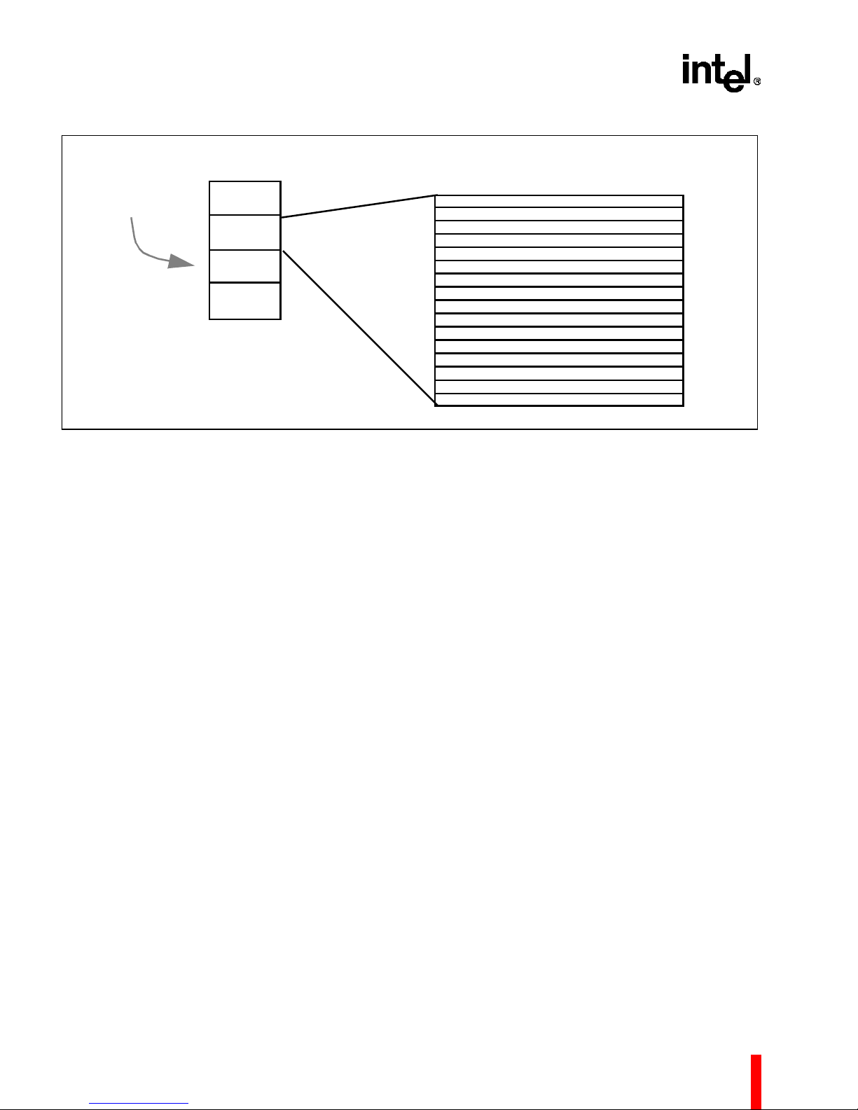
80960MC
REGISTER
ONE OF FOUR
LOCAL
REGISTER SETS
CACHE
Figure 3. Multiple Register Sets Are Stored On-Chip
1.1.7 Memory Management and Protection
The 80960MC is ideal for multitasking applications
that require software protection and a large address
space. To ensure the highes t level of performance
possible, the memory management unit (MMU) and
tran s lat io n look-aside buffer ( TL B ) a r e c on ta ine d onchip.
The 80960MC supports a conventional form of
demand-paged virtual memory in which the address
space is divided into 4-Kbyte pages. Studies indicate
that a 4-K byte page is th e op tim um siz e for a b road
range of applications.
Each page table entry includes a 2-bit page rights
field that specifies whether the page is a no-access,
read-only, or read-write page. This field is interpreted differently depending on whether the current
task (process) is executing in user or supervisor
mode, as shown below:
Rights User Supervisor
00 No Access Read-Only
01 No Access Read-Wr ite
10 Read- Only Read-Write
11 Read-Write Read-Write
LOCAL REGISTER SET
R
0
R
15
31
0
1.1.8 Floating-Point Arithmetic
In the 80960MC, floating-point arithmetic is an
integr al part of th e archite cture. Hav ing the fl oatingpoint unit integrated on-chip provides two advantages. First, it improves the performance of the chip
for floating-point applications, since no additional
bus ove r he ad is as s oc ia ted wit h fl oa ting- po in t ca lc ulations, thereby leaving more time for other bus operations such as I/O. Second, the cost of using
floating-point operations is reduced because a
separate coprocessor chip is not required.
The 80960MC floating-point (real-number) data
types include single-precision (32-bit), double-precisio n (64-bit) and extended precision (80 -bit) floatingpoint numbers. Any registers may be used to
execute floating-point operations.
The processor provides hardware support for both
mandatory and recommended portions of IEEE
Standard 754 for floating-point arithmetic, including
all arithmetic, exponential, logarithmic and other
transcendental functions. Table 3 shows execution
times for some representative instructions.
6
Page 11

80960MC
Table 3. Sample Floating-Point Execution Times
(µs) at 25 MHz
Function 32-Bit 64-Bit
Add 0.4 0.5
Subtract 0.4 0.5
Multiply 0.7 1.3
Divide 1.3 2.9
Square Root 3.7 3.9
Arctangent 10.1 13.1
Exponent 11.3 12.5
Sine 15.2 16.6
Cosine 15.2 16.6
1.1.9 Multitasking Support
Multita sking programs commonly involve the m onitoring and control of an external operation, such as
the activities of a process controller or the movements of a machine tool. These programs generally
consis t of a nu mber of proces ses that run ind ependently of one another, but share a common
database or pass data among themselves.
The 80960MC offers several hardware functions
designed to support multitasking systems. One
unique feature, called self-dispatching, allows a
processor to switch itself automatically among
scheduled tasks. When self-dispatching is used, all
the operating system is required to do is place the
task in the sc heduli ng queu e.
information by means of communication ports is
asynchronous and automatically buffered by the
processor.
Communication between tasks by means of ports
can be carried out independently of the operating
system. Once the ports have been set up by the
programmer, the processor handles the message
passing automatically.
1.1.11 High Bandwidth Local Bus
The 80960MC CPU resides on a high-bandwidth
address/data bus known as the local bus (L-Bus).
The L-Bus provides a direct communication path
between the processor and the memory and I/O
subsystem interfaces. T he processor uses th e L-Bus
to fetch instructions, manipulate memory and
respond to interrupts. L-Bus features include:
• 32-bit multiple xed address/data path
• Four-word burst capability which allows transfers
from 1 to 16 bytes at a time
• High bandwidth re ads and writes with 66.7
MBytes/s burst (at 25 MHz)
• Special signal to indicate whether a memory transaction can be cached
Table 4 defines L-bus signal n ames and functi ons;
Table 5 defines other component-support signals
such as interrupt lines.
1.1.12 Multiple Processor Support
When the processor becomes available, it
dispatches the task from the beginning of the queue
and the n exe cutes it u ntil it bec omes b lo cke d, in terrupted, or until its time-slice expires. It then returns
the task to the end of the queue (i.e., automatically
resche dules it ) and disp atches the next read y task.
During these operations, no communication betw een
the pr oc es sor an d th e op era t ing sys te m is nece ss ary
until the running task is comp lete or an interrupt is
issued .
1.1.10 Synchronization and Communication
The 80960MC also offers instructions to set up and
test semaphores to ensure that concurrent tasks
remain synchronized and no data inconsistency
results. Special data structures, known as communication ports, provide the means for exchanging
parameters and data structures. Transmission of
7
One me ans of inc rea sing the p roces sin g pow er of a
system is to run tw o or mor e proc essors in parall el.
Since microprocessors are not generally designed to
run in tandem wit h other processors, designing such
a system is us ually difficu lt an d costly.
The 80960MC solves this problem by offering a
number of functions to coordinate the actions of
multiple p r oc es s ors . First, m e ss ag es ca n be p as s ed
between processors to initiate actions such as
flushing a cache, stopping or starting another
processor, or preempting a task. The messages are
passe d on t he b us and allo w m ultip le p ro cesso rs to
run together smoothly, with rare need to lock the bus
or memory.
Page 12

80960MC
Second, a set of synchronization instructions help
maintain memory coherency. These instructions
permit several processors to modify memory at the
same time without inserting inaccuracies or ambiguities into shared data structures.
The self-dispatching mechanism — in addition to
being used in single-processor systems — provides
the m ea ns to incr ease the p erf orma nce o f a syst em
merely by adding processors. Each processor can
either work on the same pool of tasks (sharing the
same queue with other processors) or can be
restricted to its own queue.
When processors perform system operation, they
synchronize themselves by using atomic operations
and se nd ing sp ecia l mes sage s betw ee n each oth er.
In theory, changing the number of processors in a
system does not require a software change.
Software executes correctly regardless of the
number of processors in the system; systems with
more pr ocessors simply execute faster.
1.1.13 Interrupt Handling
The 80960MC can be interrupted in two ways: by the
activ atio n of o ne of fo ur inte rru pt pi ns or by se ndin g
a message on the processor’s data bus.
The 80960MC is unusual in that it automatically
hand les inter rupts on a p riority b asis and can keep
trac k of pe nding interru pts thr ough its on-c hip in terrupt controller. Two of the interrupt pins can be
configured to provide 8259A-style handshaking for
expansion beyond four interrupt lines.
An interrupt message is made up of a vector number
and an interrupt priority. When the interrupt priority is
greater than that of the currently running task, the
pro cessor accept s the inter rupt an d uses the ve ctor
as an index into the interrupt table. When the priority
of the i nt erru pt me ssa ge is below tha t of the cu rrent
task, the processor saves the information in a
section of the interrupt table reserved for pending
interrupts.
1.1.14 Debug Featu res
The 80960MC has built-in debug capabilities,
including two types of breakpoints and six trace
modes. Debug features are controlled by two
internal 3 2-bit regist ers: the Pro cess-Controls Word
and the Trace-Controls Word. By setting bits in these
contr ol w ord s , a s of t war e d ebug m o nitor ca n closel y
control how the processor responds during program
execut io n.
The 80960MC has both hardware and software
breakpoints. It provides two hardware breakpoint
registers on-chip which, by using a special
command, can be set to any value. When the
instruction pointer matches e ither br eakpo int register
value, the breakpoint handling routine is automatically called.
The 80960MC also provides software breakpoints
through the use of two instructions: MARK and
FMARK. These can be placed at any point in a
progra m and cause th e process or to halt exe cution
at that point and call the breakpoint handling routine.
The breakpoint mechanism is easy to use and
provides a pow erfu l debugg ing tool.
Tracing is available for instructions (single step
execution), calls and returns and branching. Each
trace type may be enabled separately by a special
debug instruction. In each case, the 80960MC
executes the instruction first and then calls a trace
handling routine (usually part of a software debug
monitor). Further program execution is halted until
the routine completes, at which time execution
resumes at the next instruction. The 80960MC’S
tracing mechanisms, implemented completely in
hardware, greatly simplify the task of software test
and debug.
1.1.15 Fault Detection
The 80960MC has an automatic mechanism to
handle faults. There are ten fault types include
floating point, trace and arithmetic faults. When the
processor detects a fault, it automatically calls the
appropriate fault handling routine and saves the
current instruction pointer and necessary state information to make efficient recovery possible. The
processor posts diagnostic information on th e type of
fault to a Fault Record. Like interrupt handling
routines, fault handling routines are usually written to
meet the needs of specific applications and are often
included as part of the operating system or kernel.
For ea ch of t he ten f ault ty pes, nu merous subty pes
provide specific information about a fault. For
example, a floating point fault may have the subtype
set to an Overflow or Zero-Divide fault. The fault
handle r can u se this sp ecifi c in for mati on to resp ond
correctly to the fault.
8
Page 13

80960MC
1.1.16 Inter-Ag ent C om mu nic at ions (IAC )
To coordinate their actions, processors in a multiple
proc esso r sys tem need a mean s for com muni cati ng
with e ach o ther. Th e 8096 0MC does t his th rough a
mechanism known as “IACs” — Inter-Agent Communication messages.
IAC messages cause a variety of actions including
starting and stopping processors, flushing instruction
caches and TLBs, and sending interrupts to other
proces sors in the sys tem. The up per 16 Mbytes of
the processor’s physical memory space is reserved
for se nding and receiving IAC messages.
1.1.17 Built-in Testability
Upon reset, the 80960MC auto matically conducts an
exhaus tive int ernal te st of its major bl ocks of logic.
Then, be fore e xecuting its f irst ins truction , it do es a
zero check sum on the first eight words in memory to
ensure that the memory image was programmed
correctly. When a problem is discovered at any point
during the self-test, the 80960MC asserts its
FAILURE
pin and does not begin program execution. Self test takes approximately 47,000 cycles to
com plete .
Syst em ma nufa ctur ers can us e t he 80 960M C’s self test feature during incoming parts inspection. No
specia l dia gnos ti c prog rams need to b e wri tten. The
test is both thorough and fast. The self-test capability
helps ensure that defective parts are discovered
before systems are ship ped and, on ce in the fie ld,
the self-test ma kes it easier to distinguish be tween
probl ems caus ed by proc esso r failu re and pro bl ems
resulting from other causes.
1.1.18 Comp atibil ity with 80960K-Series
Application programs written for the 80960K-Series
microprocessors can be run on the 80960MC
withou t modific ation. The 80960K- Series ins truction
set forms the core of the 80960MC’s instructions, so
binar y co m pa tibility is as su r e d.
1.1.19 CHM OS
The 80 960M C i s fa brica ted u sin g Int el’ s CH MOS IV
(Complementary High Speed Metal Oxide Semiconductor) process. The 80960MC is currently available
at 25 MHz.
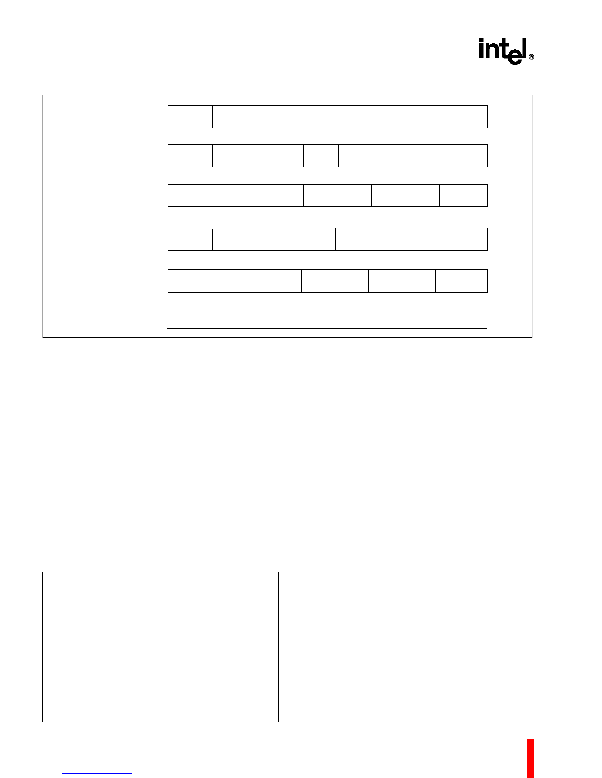
Table 4. 80960MC Pin Description: L-Bus Signals (Sheet 1 of 3)
NAME TYPE DESCRIPTION
CLK2 I SYSTEM CLOCK provides the fundamental timing f or 80960MC systems. It is
divided by t wo inside the 80960MC to generate the intern al processor clock. Refer
to Figure 16, Processor Clock Pulse (CLK2) (pg. 21)
LAD31:0 I/O
T.S.
LOCAL ADDRESS / DATA BUS carries 32-bit physical addresses and data to and
from memory. During an address (T
address (bits 0-1 indicate SIZE; see below). During a data (T
) cycle, bits 2-31 contain a physical word
a
) cycle, bits 0-31
d
contain read or write data. These pins float to a high impedance state when not
active.
Bits 0-1 comprise SIZE during a T
cycle. SIZE specifies burst transfer size in
a
words.
LAD1 LAD0
00 1 Word
0 1 2 Words
1 0 3 Words
1 1 4 Words
ALE
O
T.S.
ADDRESS LATCH ENABLE indicates the transfer of a physical address. ALE is
asserted during a T
active LOW and float s to a high impedance state duri ng a hold c y cle (T
cycle and deasserted before the beginning of the Td state. It is
a
).
h
I/O = Input/Output, O = Output, I = Input, O.D. = Open Drain, T.S. = Three-state
9
Page 14

80960MC
Table 4. 80960MC Pin Description: L-Bus Signals (Sheet 2 of 3)
NAME TYPE DESCRIPTION
ADS O
O.D.
W/R
O.D.
DT/R
O.D.
ADDRESS/DATA STATUS indicates an address state. ADS is as se r te d ev er y Ta
state and deasserted during the following T
asserted again every T
O
WRITE/READ specifies, during a Ta cycle, whether the operation is a write or read.
state where READY was asserted in the previous cycle.
d
It is latched on-chip and remains valid during T
O
DATA TRANSMIT / RECEIVE indica tes t he dire ction of data tran sf er to an d fr om
the L-Bus. It is lo w during T
it is high during T
and Td cycles for a write. DT /R never changes state when DEN
a
and Td cycles for a read or interrupt acknowledgment;
a
state. For a burst transaction, ADS is
d
cycles.
d
is asser ted.
DEN
O
O.D.
DATA ENABLE (active low) enables data t ransceivers. Th e processor asserts
DEN# during all T
and Tw states. The DEN# line is an open drain-outp ut of the
d
80960MC.
READY
LOCK
I READY indicates that data on LAD li nes can be sampled or removed . When
I/O
O.D.
READY
by inserting a wait state (T
BUS LOCK prevents bus masters from gaining control of the L-Bus during
Read/Modify/Write (RMW) cycles. The processor or any bus agent may assert
LOCK
is not asserted during a Td cycle, the Td cycle is extended to the next cycle
) and ADS is not asserted in the next cycle.
w
.
At the start of a RMW oper ation, the processor examin es the LOCK
pin is already asserted, the processor waits until it is not asserted. When the pin is
not asserted, the processor asserts LOCK
action. The pr ocessor deasserts LOCK
During the time LOCK
is asserted, a bu s agent c an perform a normal read or write
during the Ta cycle of the read trans-
in the Ta cycle of the write transaction.
but not a RMW operation.
The proc es s or al so ass er t s LO CK
Do not leave LOCK
unconnected. It must be pulled high for the processor to
durin g int err u pt - ac k no w le dg e tr an s ac tio ns .
func tion properly.
BE3:0
O
O.D.
BYTE ENABLE LINES specify the data bytes (up to four) on the bus which are
used in the current bus cycle. BE3
corresponds to LAD31:24; BE0 corresponds to
LAD7:0.
The byte enab les are provided in advance of data:
Byte enables asserted during T
Byte enables asserte d during T
specify the bytes of the first data word.
a
specify the bytes of the next data word, if any (the
d
word to be transmitted following the next assertion of READY
Byte enable s that oc cur during T
cycles that precede the last assertion of READY
d
are undefined. Byte enables are latched on-chip and remain constant from one T
cycle to the next when READ Y
is not asserted.
For reads, byte enables specify the byte(s) that the processor actually uses. L-Bus
agents are required to assert only adjacent byte ena bles (e.g., asserting just BE0
and BE2
Address bits A
is not permitted) and are required to assert at least one byte enable.
and A1 can be decoded e x ternally from the byte enables.
0
I/O = Input/Output, O = Output, I = Input, O.D. = Open Drain, T.S. = Three-state
pin. When the
).
d
10
Page 15

Table 4. 80960MC Pin Description: L-Bus Signals (Sheet 3 of 3)
NAME TYPE DESCRIPTION
HOLD/
HLDAR
I HOLD: A request from an external bus master to acquire the bus. When the
processor receives HOLD and grants bus control to anothe r master, it floats its
three-state bus li nes and op en-drain control lines, asserts HLDA and enters the T
state. When HOLD deasserts, the processor deasserts HLDA and enters the T
state.
T
a
HOLD ACKNOWLEDGE RECEIVED: Indicates that the processor has acquired
the bus. When the processor is ini tialized as th e second ary bus master this input is
interpreted as HLDAR.
Refer to Figure 18, HOLD Timing (pg. 22).
HLDA/
HOLDR
O
T.S.
HOLD ACKNOWLEDGE: Relinquishes control of the bus to another bus master.
When the processor is initialized as the primary bus mast er this output is
interpreted as HLDA. When HOLD is deasserted, the processor deasserts HLDA
and go es to either the T
or Ta state.
i
HOLD REQUEST: Indicates a request to acquire the bu s. When the processor is
initialized as the secondary bus master this output is interpreted as HOLDR.
Refer to Figure 18, HOLD Timing (pg. 22).
CACHE/
TAG
O
T.S.
CACHE indicates when an access is cacheable during a T
during any synchrono us access, such as a synchronous load or move inst ruction
used for sending an IAC message. The C ACHE signal floats to a high impedance
state when the processor is idle.
TAG is an input/output signal that, during T
and Tw cycles, identifi es the co ntents
d
of a 32-bit word as either data (TAG = 0) or an access descript or (TAG = 1).
I/O = Input/Output, O = Output, I = Input, O.D. = Open Drain, T.S. = Three-state
80960MC
or
i
cycle. It is not asserted
a
h
Table 5. 80960MC Pin Description: Support Signals (Sheet 1 of 2)
NAME TYPE DESCRIPTION
BADAC
I BAD ACCESS, when asserted in the cycle following the one in which the last
READY
of a transaction is asserted, indicates that an unrecoverable error has
occurred on the current bus tran saction or th at a synchronous load/ s tore i nstruction
has not been acknowledged.
During system reset the BADAC
signal is interpreted differently. When the signal is
high, it indicates that this processor will perform system initialization. When low,
another processor in the system will perform system initialization instead.
RESET I RESET clears the processor’s internal logic and causes it to reinitialize.
Duri ng RESET assertion, the input pins are ignored (e xcept for BADAC
IAC
/INT0), the three-state output pins are placed in a high impedance state and
other output pins are placed in their non-asserted states.
RESET must be asserted for at least 41 CLK2 cycles for a predictable RESET. The
HIGH to LOW transition of RESET should occur after the rising edge of both CLK2
and the external bus clock and before the next rising edge of CLK2.
Refer to Figure 17, RESET Signal Timing (pg. 21).
I/O = Input/Output, O = Output, I = Input, O.D. = Open Drain, T.S. = Three-state
and
11
Page 16

80960MC
Table 5. 80960MC Pin Description: Support Signals (Sheet 2 of 2)
NAME TYPE DESCRIPTION
FAILURE O
O.D.
INITI ALIZ A TION FAIL U RE indicates that the processor did not initialize correctly.
After R ESET deasserts and before the first bus t ransaction begins, FAILURE
asserts while the proces sor per forms a self-test. When the self-t est completes
successfully, then FAILURE
checksum on the first eight words of memory. When it fails, FAILURE
deasserts. Th e processor then performs a zero
asserts for a
second time and remains asserted. When it passes, system initialization continues
IAC
/INT
0
LOCAL
PROCESSOR
NUMBER
and FAILURE
I INTERAGENT COMMUNICATION REQUEST/INTERRUPT 0 indicates an IAC
message or an interrupt is pending. The bus interrupt control register determines
how t he sig nal is interpreted. To signal an interru pt or IAC re quest in a synchro nous
system, this pin — as well as the other interrupt pins — must be enabled by being
deasserted for at leas t one bus cycle and then asserted for at least one additional
remains deasserted.
bus cycle. In an asynchronous s ystem the pin must remain deasserted for at least
two bus cycles and then asserte d for at least two more bus cycles.
LOCAL PROCESSOR NUMBER - this signal is interpreted differently during
system reset. When the signal is a high voltage level it indicates that this processor
is a primary bus master (local processor number = 0). When at a low voltage level it
indicates that this pr ocesso r is a secondary bus master (local processor numb er
=1).
INT
1
INT
/INTR I INTERRUPT2/INTERRUPT REQUEST: The int errupt control register determines
2
I INTERRUPT 1, like INT0, provides direct interrupt signaling .
how this pin is interpreted. When INT
and INT
pins. When INTR, it is used to receive an interrupt request from an
1
, it has the same interpretation as the INT0
2
external interrupt controller.
INT
/INTA I/O
3
O.D.
INTERRUPT3/INTERRUPT ACKNOWLEDGE: The bus interrupt control register
determines how this pi n is interp reted. When INT
the INT
, INT1 and INT2 pins. When INTA, it is used as an output to control
0
interrupt-acknowledge transactions. The INTA
remains valid during T
cycles; as an output, it is open-drain.
d
, it has the same interpretation as
3
output is latched on-chip and
N.C. N/A NOT CONNECTED indicates pins should not be connected. Never connect any pin
marked N.C. as t hese pin s may be reserved for factory use.
I/O = Input/Output, O = Output, I = Input, O.D. = Open Drain, T.S. = Three-state
12
Page 17

80960MC
2.0 ELECTRICAL SPECIFICATIONS
2.1 Power and Grounding
The 80960MC is implemented in CHMOS IV technology and therefore has modest power requirements. Its high clock frequency and numerous
output b uffer s (ad dres s/da ta, cont rol, er ror and a rbitratio n signa ls) can cause p ower s urges as multip le
output buffers simultaneously drive new signal
levels. Fo r clean on-chip power distribution, V
V
pins separately feed the device’s functional
SS
CC
and
units. Power and ground connections must be made
to all 80960MC power and ground pins. On the
circuit board, all V
togethe r, preferably on a po wer plane; all V
pins must be strapped closely
cc
ss
pins
should be str a pp ed tog ether , p refera bl y o n a g r ou nd
plane.
2.2 Power Decoupling
Recommendations
Place a liberal amount of decoupling capacitance
near the 80960MC. When driving the L-bus the
proces sor can c aus e trans ien t po wer sur ges , part icularly when connected to a large capacitive load.
Low inductance capacitors and interconnects are
recommended for best high frequency electrical
performance. Inductance is reduced by shortening
board traces betw een the proc esso r an d deco upli ng
capacitors as much as possible.
NOTE:
Do not connect external logic to pins marked N.C.
V
CC
OPEN-DRAIN OUTPUT
220 Ω
Low Drive Network:
= 3.0 V
V
OH
= 20.7 mA
I
OL
330 Ω
Figure 4. Connection Recommendations
for Low Current Drive Network
V
CC
OPEN-DRAIN OUTPUT
180 Ω
High Drive Network:
= 3.4 V
V
OH
= 25.3 mA
I
OL
390 Ω
Figure 5. Connection Recommendations
for High Current Drive Network
2.3 Connection Recomme ndations
For reliable operation, always connect unused inputs
to an appropriate signal level. In particular, when
one or m ore inte r ru pt lines are not use d, they sh ou ld
be pulled up. No inputs should ever be left floating.
All open-drain outputs require a pull-up device.
While in most cases a simple pull-up resistor is
adequa te, a net work of pull-u p and pull -down r esistors biased to a valid V
the characteristic impedance of the circuit board is
recommended to limit noise and AC power
consumption. Figure5 and Figure 6 show recom-
mended values for the resistor network for low and
high cu rre nt drive , ass umi ng a ch arac teri stic imp edance of 100
Ω. Terminating output signals in this
fashion limits signal swing and reduces AC power
consumption.
13
(>3.0 V) and t ermin at ed in
IH
2.4 Characteristic Curves
Figure 7 shows typi cal supply current requirements
over the operating temperature range of the
processor at supply voltage (V
and Figure 9 show the typical power supply current
(I
) that the 80960MC requires at various operating
CC
frequencies when measured at three input voltage
(V
) levels and two temperatur es.
CC
For a given output current (I
Figure 10 shows the worst case output low voltage
(V
). Fi gure 11 shows the typical capacitive
OL
derating curve for the 80960MC measured from 1.5V
on the system clock (CLK) to 1.5V on the falling
edge and 1.5V on the rising edge of the L-Bus
address/data (LAD) signals.
) of 5 V. Figure 8
CC
) the curve in
OL
Page 18

80960MC
VCC = 5.0 V
380
360
340
320
25 MHz
20 MHz
16 MHz
300
280
260
240
POWER SUPPLY CURRENT (mA)
220
200
-60 -40 -20 0 20 40 60 80 100 120 140
CASE TEMPERATURE (°C)
Figure 6. Typical Supply Current vs. Case Temperature
TEMP = +22°C
@5.5V
@5.0V
@4.5V
400
380
360
340
320
300
280
260
240
TYPICAL SUPPLY CURRENT (mA)
220
200
180
16 20 25
OPERATING FREQUENCY (MHz)
Figure 7. Typical Current vs. Frequency (Room Temp)
14
Page 19
80960MC
TEMP = +22°C
@5.5V
@5.0V
@4.5V
Figure 8. Typical Current vs. Frequency (Hot Temp)
380
360
340
320
300
280
260
240
220
TYPICAL SUPPLY CURRENT (mA)
200
180
160
16 20 25
OPERATING FREQUENCY (MHz)
(TEMP = +85°C, V
CC
= 4.5V)
0.8
0.6
0.4
0.2
0.0
01020304050
OUTPUT LOW VOLT AGE (V)
OUTPUT LOW CURRENT(mA)
Figure 9. Worst-Case Voltage vs. Output Current
on Open-Drain Pins
(TEMP = +85°C, V
CC
= 4.5V)
30
FALLING
25
20
15
10
VALID DELAY(ns)
5
THREE-STATE OUTPUT
RISING
0
020406080100
CAPACITIVE LOAD(pF)
Figure 10. Capacitive Derating Curve
15
Page 20

80960MC
2.5 Test Load Circuit
Figure 12 illustrates the load circuit used to test the
80960MC’s three-state pins; Figure 13 shows the
load circuit used to test the open drain outputs. The
open drain test uses an active load circuit in the form
of a matched diode bridge. Since the open-drain
outputs sink current, only the I
are necessary and the I
legs are not used. When
OH
legs of the bridg e
OL
the 80960MC driver under test is turned off, the
outpu t pin is pu lled up to V
(i.e., VOH). Diode D
REF
is turned o ff an d the IOL current source flows through
diode D
.
2
When the 80960MC open-drain driver under test is
on, diode D
being tested drops to V
is a lso on a nd the v oltage on the pin
1
. Di ode D2 turns off and I
OL
OL
flows through diode D1.
THREE-STATE OUTPUT
C
L
C
= 50 pF for all signals
L
1
Figure 11. Test Load Circuit for Three-State
Output Pins
I
OL
OPEN-DRAIN OUTPUT
= V
CC
D
2
C
L
CL = 50 pF for all signals
D
1
IOL Tested at 25 mA
V
REF
D1 and D2 are matched
Figure 12. Test Load Circuit for Open-Drain
Output Pins
16
Page 21

80960MC
2.6 Absolute Maximum Ratings
NOTICE: This is a production data sheet. The specifi-
cations are subject to change without notice.
*WARNING: Stressing the device beyond the
Operating Temperature (PGA) ...... 0° C to +85° C Case
Storage Temperature..................... –65° C to +150° C
Voltage on Any Pin ........................ –0.5 V to VCC +0.5 V
Power Dissipation .......................... 2.5 W (25 MHz)
“Absolute Maximum Ratings” may cause
permanent damage. These are st ress ratings
only . Operat ion beyond the “Operatin g Conditions” is no t recommended and extended
exposure beyond the “Operating Conditions”
may affect device reliability.
2.7 DC Characteristics
PGA: 80960MC (25 MHz) T
Symbol Parameter Min Max Units Notes
V
IL
V
IH
V
CL
V
CH
V
OL
V
OH
I
CC
Input Low Voltage –0.3 +0.8 V
Input High Voltage 2.0 VCC + 0.3 V
CLK2 Input Low Voltage –0.3 +0.8 V
CLK2 Input High Voltage 0.55 V
Output Low Voltage 0.45 V (1,2)
Out put High Voltage 2.4 V (3,4)
Power Supply Current:
16 MHz
20 MHz
25 MHz
I
LI
I
LO
C
IN
C
O
C
CLK
NOTES:
1. For three-state outputs, this parameter is measured at:
Address/Data 4.0 mA
Controls 5.0 mA
2. For open-drain outputs 25 mA
3. This parameter is measured at:
Address/Data –1.0 mA
Controls –0.9 mA
ALE
4. Not measured on open-drain outputs.
5. Measured at worst case frequency, V
in Figure 12 and Figure 13. Figure 7, Figure 8 and Figure 9 indicate typical values.
6. Input, output and clock capacitance are not tested.
Input Leak age Curr ent ±15 µA 0 ≤ VIN ≤ V
Output Leakage Current ±15 µA 0.45 ≤ VO ≤ V
Input Capacitance 10 pF fC = 1 MHz (6)
Output Capacitance 12 pF fC = 1 MHz (6)
Clock Capacitance 10 pF fC = 1 MHz (6)
–5.0 mA
= 0° C to +85° C, VCC = 5V ± 5%
CASE
Table 6. DC Characteristics
CC
and temperature, with device operating and outputs loaded to the test conditions
CC
VCC + 0.3 V
315
360
420
mA
mA
mA
(5)
(5)
(5)
CC
CC
17
Page 22
80960MC
2.8 AC Specifications
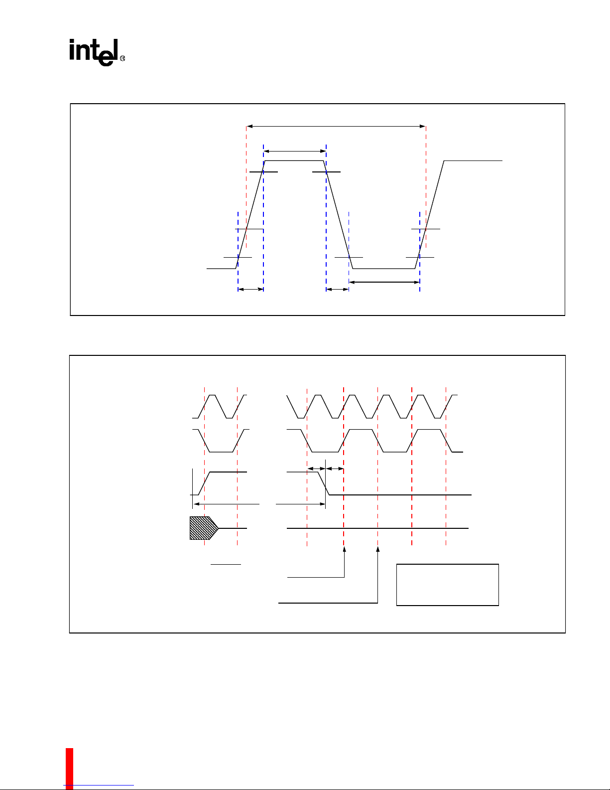
This sect ion des cribes the AC specif icatio ns for th e
80960MC pins. All input and output timings are specified relative to the 1.5 V level of th e rising ed ge of
CLK2. Fo r output tim ings the spec ifications refe r to
the time it takes the signal to reach 1.5 V.
EDGE
CLK2
0.8V
OUTPUTS:
LAD 31:0
ADS
W/R, DEN
BE3:0
HLDA/HOLDR
CACHE
LOCK, INTA
ABC
1.5V
T
1.5V 1.5V 1.5V
T
6
1.5V
8
VALID OUTPUT
T
8
T
13
For input timings the specifications refer to the time
at which the signal reaches (for input setup) or
leaves (for hold time) the TTL levels of LOW (0.8 V)
or HIGH (2.0 V). All AC testing should be done with
input voltages of 0.4 V and 2.4 V, except for the
clock (CLK2), which should be tested with input
voltages of 0.45 V and 0.55V
D
T
9
A
1.5V
BC
T
14
CC
.
ALE
DT/R
INPUTS:
LAD31:0
BADAC
IAC/INT0, INT1
INT2/INTR, INT3
HOLD, HLDAR
LOCK
READY
1.5V
1.5V
T
7
T
6
10
12
VALID OUTPUT
T
11
T
11
1.5V 1.5V
T
2.0V 2.0V
0.8V 0.8V
T
2.0V 2.0V
0.8V 0.8V
VALID INPUT
T
9
Figure 13. Drive Levels and Timing Relationships for 80960MC Signals
18
Page 23
80960MC
CLK2
CLK
LAD
(31-0)
ALE#
ADS#
BE(0:3)#
W/R#
DT/R
DEN#
READY#
T
ad r
T
3
T
2
T
T
13
6
Address Data
T
8
T
7
T
13
T
6
T
T
1
T
9
T
14
T
14
T
6
T
10
T
9
T
T
11
12
T
T
11
T
9
T
ad r
T
6
T
13
Address
T
8
T
7
T
13
T
6
T
6
T
9
T
14
T
6
T
T
12
T
d
Data
T
11
T
T
9
T
9
T
T
11
12
Figure 14. Timing Relationship of L-Bus Signals
CLK2
CLK
Figure 15. System and Processor Clock Relationship
19
Bus
State
T
a
Bus
State
T
dr
Bus
State
T
A4484-01
Page 24
80960MC
Table 7. 80960MC AC Characteristics (25 MHz)
Symbol Parameter Min Max Units Notes
Input Clock
T
T
T
T
T
Processor Clo ck Period (CLK2) 20 125 ns VIN = 1.5V
1
Processor Clock Low Time (CLK2) 5 ns VIL = 10% Point = 1.2V
2
Processor Clock High Time (CLK2) 5 ns VIH = 90% Point = 0.1V + 0.5 V
3
Processor Clock Fall Tim e (CLK2) 10 ns VIN = 90% Point to 10% Point (1)
4
Processor Clock Rise Time (CLK2) 10 ns VIN = 10% Point to 90% Point (1)
5
CC
Synchronous Outputs
T
T
T
T
T
T
Output Valid Delay 2 18 ns
6
HLDA Ou tput Valid Delay 4 23 ns
6H
ALE Width 12 ns
7
ALE Output Valid Delay 2 18 ns
8
Outp ut Floa t Delay 2 18 ns (2)
9
HLDA Output Float Delay 4 2 0 ns (2)
9H
Synchr onous Inputs
T
T
Input Setup 1 3 ns (3)
10
Input Hold 5 ns (3)
11
T
11H
T
T
T
T
T
T
NOTES:
1. Clock rise and fall times are not tested.
2. A float condition occurs when the maximum output current becomes less than I
should not be longer than the valid delay.
3. LAD31:0, BADAC
chronous or asynchronous.
HOLD Input Hold 4 ns
Input Setup 2 7 ns
12
Setup to ALE Inac tiv e 8 ns
13
Hold after ALE Inactive 8 ns
14
Reset Hold 3 ns
15
Reset Setup 5 ns
16
Reset Width 820 ns 41 CLK2 Periods Minimum
17
, HOLD, LOCK and READY are synchronous inputs. IAC/INT0, INT1, INT2/INTR and INT3 may be syn-
. Float delay is not tested; however, it
LO
20
Page 25
80960MC
T
1
T
3
HIGH LEVEL (MIN) 0.55V
LOW LEVEL (MAX) 0.8V
CLK2
CLK
1.5 V
10%
90%
T
4
FIRST
ABCDA
CC
T
5
Figure 16. Processor Clock Pulse (CLK2)
...
...
T
2
...
RESET
T
17
OUTPUTS
INIT PARAMETERS (BADAC
/IAC) MUST BE SET UP 8 CLOCKS
INT
0
PRIOR TO THIS CLK2 EDGE
INIT PARAMETERS MUST BE HELD
BEYOND THIS CLK2 EDGE
...
,
Figure 17. RESET Signal Timing
T
15T16
T15 = RESET HOLD
= RESET SETUP
T
16
T
= RESET WIDTH
17
21
Page 26

80960MC
CLK2
CLK
HOLDR
HOLD
HLDA
HLDAR
Th
T
6h
T
12
T
6h
T
12
Primary
HOLD
HLDA
T
9h
T
11h
D
D
ThThTh
T
9h
T
11h
Secondary
HOLDR
HOLDAR
Delay of 5 ns Minimum
Figure 18. HOLD Timing
2.9 D es i gn Consider ations
Inp ut ho ld time s can be disr e g ar d ed by th e desi gner
whenever the input is removed because a subsequent output from the processor is deasserted (e.g.,
becomes deasserted).
DEN
In other words, whenever the processor generates
an output that indicates a transition into a subsequent state, the processor must have sampled any
inputs for the previous state.
Similarly, whenever the processor generates an
outpu t that indicates a trans ition into a subsequent
state, any outputs that are specified to be three
stated in this new state are guaranteed to be three
stated.
is Required
A4490-01
3.0 MECHANICAL DATA
3.1 Packaging
The 80960MC is available in one package type: a
132-lead ceramic pin-grid array (PGA). Pins are
arranged 0.100 inch (2.54 mm) center-to-center, in a
14 by 14 mat rix, th re e row s aro und (see Figure 20).
Dimensions for the PGA package type is given in the
Packaging
Intel
3.1.1 Pin Assign me nt
Figure 21 shows the view from the PGA bottom (pins
facing up). Table 8 and Table 9 list the function of
each PGA pin.
handbo ok (Or d er #24080 0) .
22
Page 27

80960MC
1
2
3
4
5
6
7
8
9
10
11
12
13
14
ABCDEFGHJK LMNP
Figure 19. 132-Lead Pin-Grid Array (PGA) Package
23
Page 28

80960MC
1413121110987654321
P
CC
N.C.N.C.N.C.N.C.N.C.N.C.N.C.N.C.N.C.N.C.N.C.V
SS
CC
V
V
N
SS
N.C.N.C.N.C.N.C.N.C.N.C.N.C.N.C.N.C.N.C.N.C.N.C.N.C.V
M
N.C.
V
V
SS
CC
V
V
CC
SS
N.C.N.C.N.C.N.C.
V
V
SS
CC
N.C.N.C.N.C.
L
V
N.C.DEN
CC
V
SS
N.C.N.C.
K
V
FAILBE
3
SS
V
CC
N.C.N.C.
J
DT/R
BE
V
SS
2
N.C.N.C.N.C.
H
W/R
LOCKBE
0
N.C.N.C.N.C.
G
READYLAD
30
BE
1
N.C.N.C.N.C.
F
LAD
31
29
N.C.N.C.N.C.
CACHE
LAD
E
LAD
28
LAD
LAD
27
26
N.C.N.C.
V
SS
D
HLDAADSALE
V
CC
N.C.N.C.
C
V
BADACHOLD LAD
25
V
CC
LAD
SS
LAD
20
13
LAD
LAD
3
8
V
V
CC
SS
INT
3
INT
INT
0
1
B
V
LAD
LAD
23
22
24
18
21
12
15
6
10
2
CLK2
LAD
LAD
LAD
LAD
LAD
LAD
LAD
LAD
RESETLAD
0
SS
A
V
CC
19
SS
LAD
17
16
LAD
LAD
V
LAD
LAD
LAD
11
14
9
LAD
LAD
5
7
LAD
LAD
1
4
INT
V
CC
2
P
N
M
L
K
J
H
G
F
E
D
C
B
A
Figure 20. 80960MC PGA Pinout—View from Bottom (Pins Facing Up)
24
1413121110987654321
Page 29

14 13 12 11 10 9 8 7 6 5 4 3 2 1
80960MC
P
V
CCVSS
N
N.C. N.C. N.C. N.C. N.C. N.C. N.C. N.C. N.C. N.C.
N.C. N.C. N.C. N.C. N.C. N.C. N.C. N.C. N.C. N.C. N.C. V
N.C. N.C.
N.C.
CC
V
SS
M
N.C. N.C. N.C.
V
CCVSS
N.C. N.C. N.C. N.C.
V
CCVSS
V
SS
VCCN.C.
L
N.C. N.C.
V
SS
V
CC
N.C. DEN
K
N.C. N.C.
V
CC
V
SS
FAIL BE
3
J
N.C. N.C. N.C.
V
SS
BE2DT/R
H
N.C. N.C. N.C.
LOCK BE
W/R
0
G
N.C. N.C. N.C.
BE
READY LAD
1
30
F
N.C. N.C. N.C.
x80960MC-25
XXXXXXXX
XXXXXX
XXXXXX
CACHE LAD31LAD
29
E
V
N.C. N.C.
SS
LAD27LAD26LAD
28
D
N.C. N.C.
V
CC
HLDA ADS ALE
C
INT0INT1INT
V
V
CC
LAD3LAD
SS
3
LAD
8
13
LAD
V
V
SS
20
BADAC HOLDLAD
CC
25
B
V
RESET LAD
SS
0
LAD2LAD6LAD10LAD12LAD15LAD18LAD21LAD22LAD24LAD
CLK2
23
A
VCCINT
LAD1LAD4LAD5LAD7LAD9LAD11LAD14LAD16LAD17LAD
2
VSSV
19
CC
P
N
M
L
K
J
H
G
F
E
D
C
B
A
14 13 12 11 10 9 8 7 6 5 4 3 2 1
Figure 21. 80960MC PGA Pinout—View from Top (Pins Facing Down)
25
Page 30

80960MC
3.2 Pinout
Table 8. 80960MC PGA Pinout — In Pin Order
Pin Signal Pin Signal Pin Signal Pin Signal
A1 V
A2 V
CC
SS
A3 LAD
A4 LAD
A5 LAD
A6 LAD
A7 LAD
A8 LAD
A9 LAD
A10 LAD
A11 LAD
A12 LAD
A13 INT
A14 V
/INTR D12 V
2
CC
B1 LAD
B2 LAD
B3 LAD
B4 LAD
B5 LAD
B6 LAD
B7 LAD
B8 LAD
B9 LAD
B10 LAD
19
17
16
14
11
9
7
5
4
1
23
24
22
21
18
15
12
10
6
2
C6 LAD
C7 LAD
C8 LAD
C9 LAD
C10 V
C11 V
20
13
8
3
CC
SS
C12 I NT3/INTA J1 DT/R N2 N.C.
C13 INT
C14 IAC/INT
1
0
D1 ALE J12 N.C. N 5 N.C.
D2 ADS J13 N.C. N 6 N.C.
D3 HLDA/HOLDR J 14 N.C. N7 N.C.
CC
D13 N.C. K2 FAILURE N9 N.C.
D14 N.C. K3 V
E1 LAD
E2 LAD
E3 LAD
28
26
27
E12 N.C. L1 DEN N14 N.C.
E13 V
SS
E14 N.C. L3 V
F1 LAD
F2 LAD
29
31
F3 CACHE/TAG L14 N.C. P5 N.C.
B11 CLK2 F12 N.C. M1 N.C. P6 N.C.
B12 LAD
0
F13 N.C. M2 V
B13 RESET F14 N.C. M3 V
B14 V
SS
G1 LAD
30
C1 HOLD/HLDAR G2 READY
C2 LAD
25
C3 BADAC
C4 V
C5 V
NOTES: Do not connect any external logic to any pins marked N.C.
CC
SS
G3 BE
1
G12 N.C. M7 N.C. P12 N.C.
G13 N.C. M8 N.C. P13 V
G14 N.C. M9 N.C. P14 V
H1 W/R M10 V
H2 BE
0
M11 V
H3 LOCK M12 N.C.
H12 N.C. M13 N.C.
H13 N.C. M14 N.C.
H14 N.C. N1 V
J2 BE
J3 V
K1 BE
K12 V
2
SS
3
SS
CC
N3 N.C.
N4 N.C.
N8 N.C.
N10 N.C.
N11 N.C.
K13 N.C. N12 N.C.
K14 N.C. N13 N.C.
L2 N.C. P1 V
P2 N.C.
P3 N.C.
L12 V
CC
SS
L13 N.C. P4 N.C.
P7 N.C.
P8 N.C.
P9 N.C.
P10 N.C.
M4 V
M5 V
CC
SS
SS
CC
M6 N.C. P11 N.C.
SS
CC
SS
CC
SS
CC
26
Page 31

Table 9. 8096 0MC PGA Pinout — In Signal Order
Signal Pin Signal Pin Signal Pin Signal Pin
ADS
ALE
BADAC
BE
0
BE
1
BE
2
BE
3
CACHE F3 LAD
CLK2 B11 LAD
DEN
DT/R
FAILURE
HLDA/HOLDR D3 LAD
HOLD/HLDAR C1 LAD
IAC
/INT
0
INT
1
INT
/INTR A13 LAD
2
INT
/INTA C12 LOCK H3 N.C. N6 V
3
LAD
0
LAD
1
LAD
2
LAD
3
LAD
4
LAD
5
LAD
6
LAD
7
LAD
8
LAD
9
LAD
10
LAD
11
LAD
12
LAD
13
LAD
14
NOTE: Do not connect external logic to any pins marked N.C.
D2 LAD
D1 LAD
C3 LAD
H2 LAD
G3 LAD
J2 LAD
K1 LAD
L1 LAD
J1 LAD
K2 LAD
C14 LAD
C13 LAD
15
16
17
18
19
20
21
22
23
24
25
26
27
28
29
30
31
B12 N.C. D13 N.C. N7 V
A12 N.C. D14 N.C. N8 V
B10 N.C. E12 N.C. N9 V
C9 N.C. E14 N.C. N10 V
A11 N.C. F12 N.C. N11 V
A10 N.C. F13 N.C. N12 V
B9 N.C. F14 N.C. N13 V
A9 N.C. G12 N.C. N14 V
C8 N.C. G13 N. C. P2 V
A8 N.C. G14 N.C. P3 V
B8 N.C. H12 N.C. P4 V
A7 N.C. H13 N.C. P5 V
B7 N.C. H14 N.C. P6 V
C7 N.C. J12 N.C. P7 V
A6 N.C. J13 N.C. P8 W/R H1
B6 N.C. J14 N.C. P9
A5 N.C. K13 N.C. P10
A4 N.C. K14 N.C. P11
B5 N.C. L13 N.C. P12
A3 N.C. L14 N.C. L2
C6 N.C. M 1 READY G2
B4 N.C. M6 RESET B13
B3 N.C. M7 V
B1 N.C. M8 V
B2 N.C. M9 V
C2 N.C. M12 V
E2 N.C. M13 V
E3 N.C. M14 V
E1 N.C. N2 V
F1 N.C. N3 V
G1 N.C. N4 V
F2 N.C. N5 V
CC
CC
CC
CC
CC
CC
CC
CC
CC
CC
CC
CC
SS
SS
SS
SS
SS
SS
SS
SS
SS
SS
SS
SS
SS
80960MC
A1
A14
C4
C10
D12
K12
L3
M2
M5
M11
P1
P14
A2
B14
C5
C11
E11
J3
K3
L12
M3
M4
M10
N1
P13
27
Page 32

80960MC
3.3 Package Thermal Specification
Maximum allowable ambient temperature (T
permitted without exceeding T
The 80 960MC is sp ecified for ope ration whe n case
temp eratur e is within the range 0°C to 85°C (PGA).
Measure case temperature at the top center of the
package. Ambient temperature can be calculated
graphs in Figure 23, Figure 24 and Figure 25. The
curves assume the maximum permitted supply
current (I
T
CASE
) at each speed, VCC of +5.0 V and a
CC
of +85° C (PGA).
from:
•T
•T
•T
Values for θ
Table 10 for the PGA package. The PGA’ s θ
= TC + P*θ
J
= TJ + P*θ
A
= TA + P*[θja−θjc]
C
ja
jc
ja
and θjc for various airflows are g iven in
can
ja
be reduced by adding a heatsink.
Table 10. 80960MC PGA Packag e Thermal Characteristics
Thermal Resistance — °C/Watt
Airflow — ft./min (m/sec)
Parameter
θ Junction-to-Case2222222
0
(0)
50
(0.25)
100
(0.50)
200
(1.01)
400
(2.03)
600
(3.04)
800
(4.06)
is shown by the
C
)
A
θ Case-to-Ambient
19 18 17 15 12 10 9
(No Heatsink)
θ Case-to-Ambient
16 15 14 12 9 7 6
(Omnidirectional
Heatsink)
θ Case-to-Ambient
15 14 13 11 8 6 5
(Unid ire ct iona l
Heatsink)
NOTES:
1. This table applies to 80960MC PGA plugged into socket or soldered directly to board.
2. θ
= θJC + θ
3. θ
JA
J-CAP
θ
J-PIN
θ
J-PIN
CA
= 4°C/W (approx.)
= 4°C/W (inner pins) (approx.)
= 8°C/W (outer pins) (approx.)
θ
J-PIN
θ
JA
θ
JC
θ
J-CAP
28
Page 33

85
80
75
C)
70
o
65
60
55
50
TEMPERATURE (
45
40
0 100 200 300 400 500 600 700 800
AIRFLOW (ft/min)
80960MC
PGA with no
heatsink
PGA with omnidirectional heatsink
PGA with unidirectional heatsink
Figure 22. 25 MHz Maximum Allowable Ambient Temperature
29
Page 34

80960MC
4.0 WAVEFORMS
The following figures present waveforms for various transactions on the 80960MC’S local bus:
• Figure 23, Non-Burst Read and Write Transactions Without Wait States (pg. 30)
• Figure 24, B urst Read and Wr ite Transaction Without Wait States (pg. 31 )
• Figure 25, Burst Write Transaction with 2, 1, 1, 1 Wait States (pg. 32)
• Figure 26, A c cesses Generated by Qu ad Word R ead Bus Request, Misaligned Two Bytes from Quad Word
Boundary (1, 0, 0, 0 Wait States) (pg. 33)
• Figure 27, Interrupt Acknowledge Transaction (pg. 34)
• Figure 28, Bus Exchange Transaction (PBM = Primary Bus Master, SBM = Secondary Bus Master) (pg. 35)
CLK2
CLK
LAD31:0
ALE
ADS
BE3:0
W/R
DT/R
T
a
T
d
T
r
T
a
T
d
T
r
DEN
READY
Figure 23. Non-Burst Read and Write Transactions Without Wait States
30
Page 35

80960MC
CLK2
CLK
LAD31:0
ALE
ADS
BE3:0
W/R
DT/R
T
a
T
d
T
d
T
r
T
a
T
d
T
d
T
d
T
d
T
r
DEN
READY
Figure 24. Burst Read and Write Transaction Without Wait States
31
Page 36
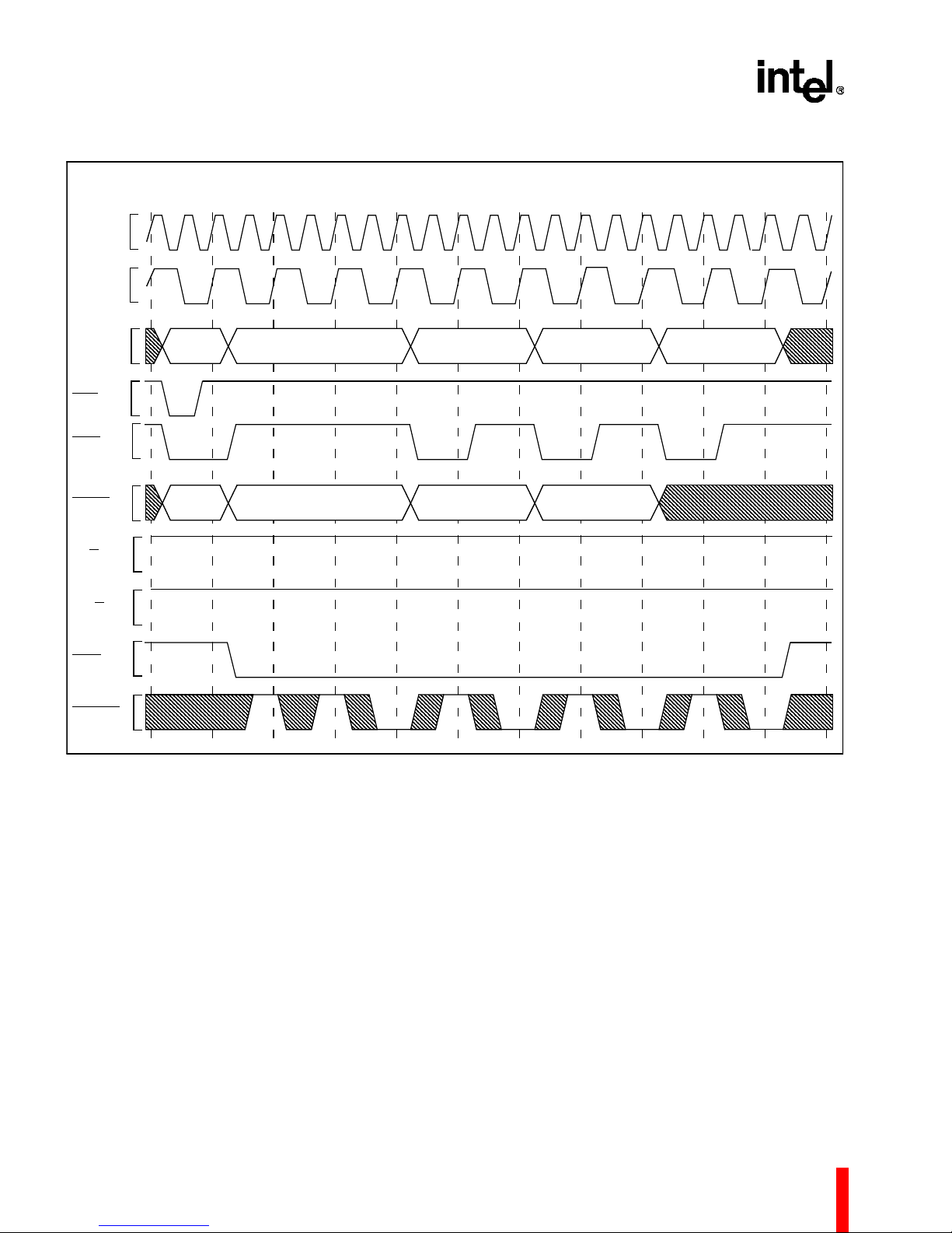
80960MC
CLK2
CLK
LAD31:0
ALE
ADS
BE3:0
W/R
DT/R
T
a
T
w
T
w
T
d
T
T
w
d
T
w
T
d
T
w
T
d
T
r
DEN
READY
Figure 25. Burst Write Transaction with 2, 1, 1, 1 Wait States
32
Page 37
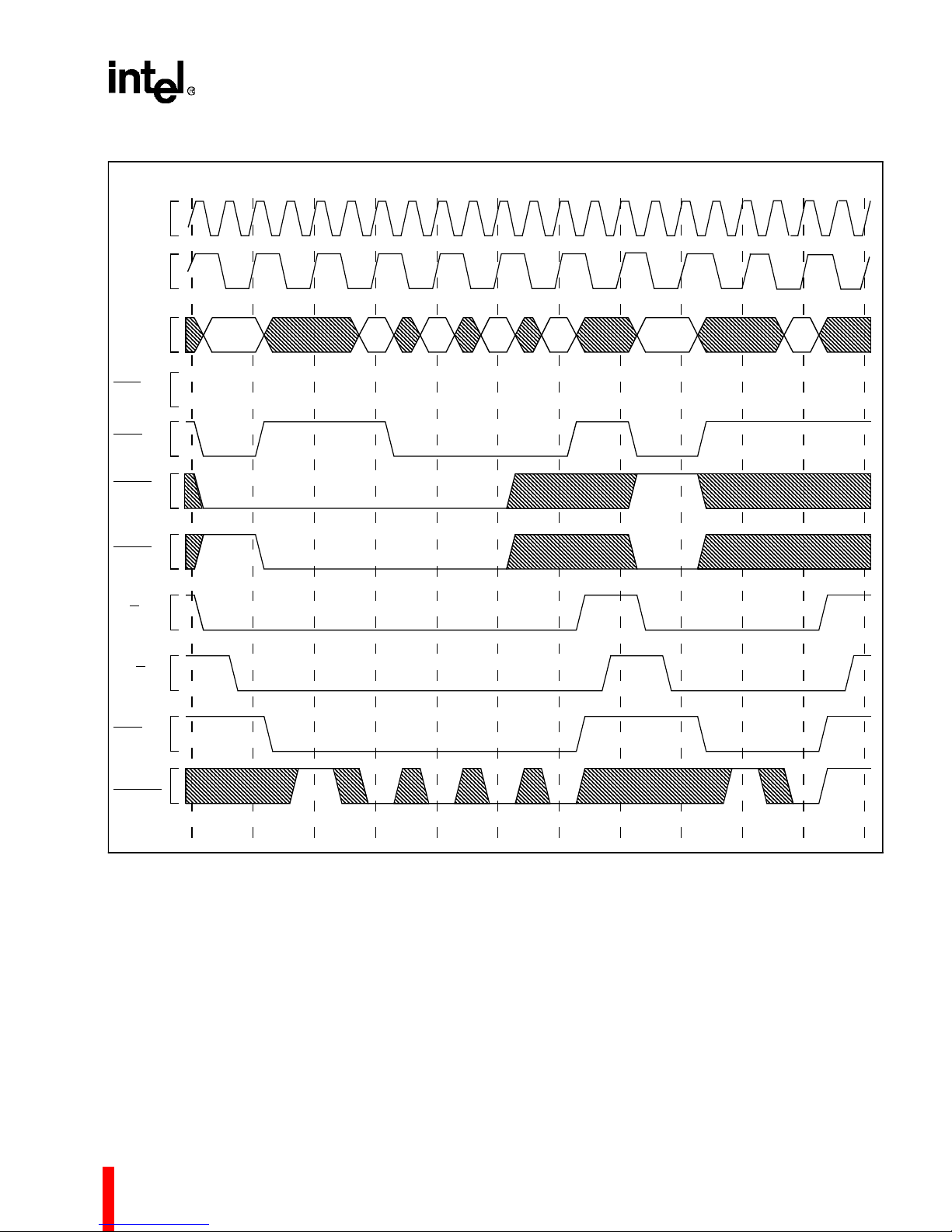
80960MC
CLK2
CLK
LAD31:0
ALE
ADS
BE3:2
BE1:0
W/R
T
a
T
w
T
d
T
d
T
T
d
d
T
r
T
a
T
w
T
d
T
r
DT/R
DEN
READY
Figure 26. Accesses Generated by Quad Word Read Bus Request, Misaligned Two Bytes from Quad
Word Boundary (1, 0, 0, 0 Wait States)
33
Page 38
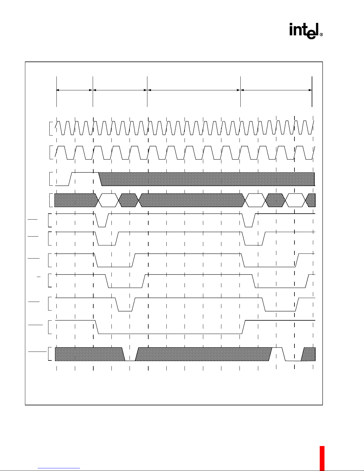
80960MC
CLK2
CLK
INTR
LAD31:0
ALE
ADS
PREVIOUS
CYCLE
T
X
INTERRUPT
ACKNOWLEDGEMENT
CYCLE 1
T
T
X
a
ADDR
IDLE
(5 BUS STATES)
T
T
d
T
r
T
I
T
I
T
I
T
I
I
INTERRUPT
ACKNOWLEDGEMENT
CYCLE 2
T
a
ADDR
T
T
w
d
VECTOR
T
r
INTA
DT/R
DEN
LOCK
READY
NOTE:
INTR can go low no sooner than the input hold time following the beginning of interrupt acknowledgment cycle 1.
For a second interrupt to be acknowledged, INTR must be low for at least three cycles before it can be reasserted.
Figure 27. Inter rupt A ck nowl edge Tran sa ct ion
34
Page 39

80960MC
PBM BUS
STATE
SBM BUS
STATE
CLK
LAD
31
LAD
W/R#
PBM ALE#
SBM ALE#
READY#
SBM
HOLDR
PBM
HOLD
PBM
HLDA
SBM
HLDAR
T
a d h
ThrThrT
_
Addr
0
T
Data
ThThThThT
h
T
hr
T
a
Addr
T
h
T
d
Data
T
T
a d
h
ThrThrThrT
T
r
Addr
T
d
Data
T
Data
T
T
h
h
T
a
hr
Addr
T
h
TdT
T
h
d
DataData
T
T
i
h
T
T
r
i
A4492-01
Figure 28. Bus Exchange Transaction (PBM = Primary Bus Master, SBM = Secondary Bus Master)
5.0 REVISION HISTORY
To address the fact that many of the package prefix variables have changed,
all package prefix variables in this document are now indicated with an "x".
5.0 REVISION HISTORY
35
 Loading...