

Page 1
80960KB
EMBEDDED 32-BIT MICROPROCESSOR
WITH INTEGRA TE D FLOATING-POINT UNIT
80960KB
High-Performance Embedded
■
Architecture
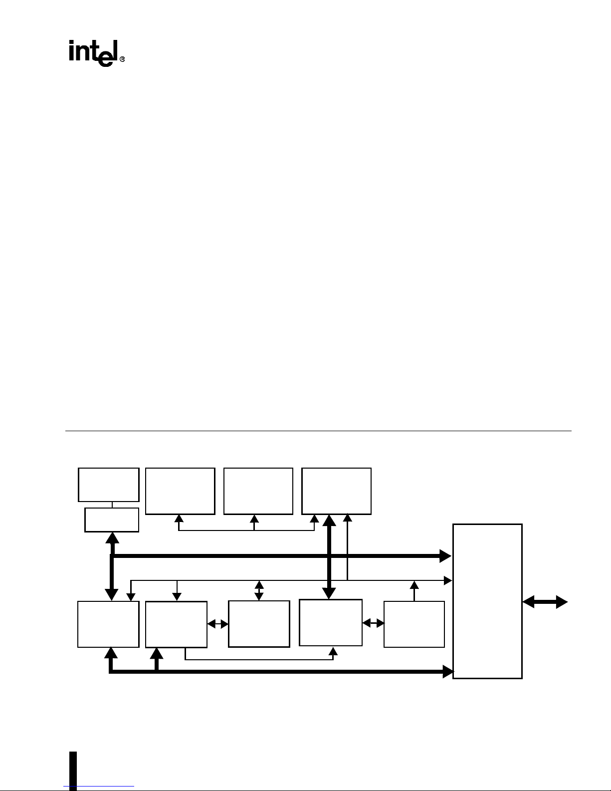
— 25 MIPS Burst Execution at 25 MHz
— 9.4 MIPS* Sustained Execution at
25 MHz
■ 512-Byte On-Chip Instruction Cache
— Direct Mapped
— Parallel Load/Decode for Uncached
Instructions
■ Multiple Register Sets
— Sixteen Global 32-Bit Registers
— Sixteen Local 32-Bi t Registers
— Four Local Register Sets Stored
On-Chip
— Register Scoreboarding
■ 4 Gigabyte, Linear Address Space
■ Pin Compatible with 80960KA
FOUR
80-BIT FP
REGISTERS
80-BIT
FPU
SIXTEEN
32-BIT GLOBAL
REGISTERS
64- BY 32-BIT
LOCAL
REGISTER
CACHE
■ Built-in I nterrupt Controller
— 31 Priority Levels, 256 Vector s
— 3.4 µs Latency @ 25 MHz
■ Easy to Use, High Bandwidth 32-Bit Bus
— 66.7 Mbytes/s Burst
— Up to 16 Bytes Transferred per Burst
■ 132-Lead Packages:
— Pin Grid Array (PGA)
— Plastic Quad Flat-Pack (PQFP)
■ On-Chip Floati ng Point Unit
— Supports IEEE 754 Floating Point
Standard
— Four 80-Bit Registers
— 13.6 Mill ion Whetstones/s (Single
Precision) at 25 MHz
32-BIT
INSTRUCTION
EXECUTION
UNIT
INSTRUCTION
FETCH UNIT
512-BYTE
INSTRUCTION
CACHE
Figure 1. The 80960KB Processor’s Highly Parallel Architecture
© INTEL CORPORATION, 2004 August, 2004 Order Number: 270565-008
INSTRUCTION
DECODER
MICRO-
INSTRUCTION
SEQUENCER
MICRO-
INSTRUCTION
ROM
32-BIT
BUS CONTROL
LOGIC
32-BIT
BURST
BUS
Page 2

Information in this document is provided in connection with Intel products. No license, express or implied, by
estopp el or otherw ise, to any intellect ual proper ty rights is granted by this documen t. Except as provided in
Intel’s Terms and Conditions of Sale for such products, Intel assumes no liability whatsoever, and Intel
disclaims any express or implie d warranty, relating to sale and/or use of Intel products inc luding liabi lity or
warrant ie s relat ing to fitnes s for a part icula r pu rpos e, mer chan tabil ity, or infri ngem ent of any pa tent, copy right
or other intellectual property right. Intel products are not intended for use in medical, life saving, or life
sus taining applications. Intel may make changes to specifications and product descriptions at any time, without
notice. Contact your local I ntel sales office or your distributor to obtain th e latest specificat ions and befo re
placing your product order.
Intel retains the right to make changes to specifications and product descriptions at any time, without notice.
*Third party brands and names are the property of their respective owners.
Copies of documents which have an ordering number and are referenced in this document, or other Intel
literature, may be obtained from:
Intel Corporation
P.O. Box 7641
Mt. Prospect IL 60056-7641
or call 1-800-879-4683.
Many documents are available for download from Intel’s website at http:\\www.intel.com.
Copyright © Intel Corporation 1997, 2004
Page 3

Contents
80960KB
EMBEDDED 32-BIT MICROPROCESSOR
1.0 THE i960® PROC ESSOR . .... .... ........... ............ ... ............ .... ........... .... ........... .... ............ ........... .... ........... ... 1
1.1 Key Performance Features ................................................................................................................. 2
1.1.1 Memory Space And Addressing Modes ................................................................................... 4
1.1.2 Data Types ............................................................................................................................... 4
1.1.3 Large Register Set ................................................................................................................... 4
1.1.4 Multiple Register Sets .............................................................................................................. 5
1.1.5 Instruction Cache ..................................................................................................................... 5
1.1.6 Register Scoreboarding ...........................................................................................................5
1.1.7 High Bandwidth Local Bus .......................................................................................................6
1.1.8 Interrupt Handling ....................................................................................................................6
1.1.9 Debug Features ....................................................................................................................... 6
1.1.10 Fault Detection .......................................................................................................................7
1.1.11 Built-in Testability ...................................................................................................................7
2.0 ELECTRIC AL SPECI FIC ATIONS .... .... .... ........... .... ............ .... ........... .... ........... ............ .... ................... ....10
2.1 Power and Grounding .......................................................................................................................10
2.2 Power Decoupling Recommendations .............................................................................................10
2.3 Connection Recommendations ........................................................................................................ 11
2.4 Characte ris ti c Curves ........ ........... .... ........... .... ............ .... ........... ........... .... ............ .... ............... .... .... 11
2.5 Test Load Circuit ............................................................................................................................... 14
2.7 DC Characteristics ............................................................................................................................ 15
2.6 Absolu te Max im um Ra tin gs ... ... .... ............ ... ............ ........... .... ............ ... ............ .... ........... ........ .... ... . 15
2.8 AC Specifications ............................................................................................................................. 16
2.8.1 AC Specification T a bles ......................................................................................................... 17
3.0 MECHANICAL DATA ................................................................................................................................ 21
3.1 Packaging ......................................................................................................................................... 21
3.1.1 Pin Assignment ...................................................................................................................... 21
3.2 Pinout ...............................................................................................................................................25
3.3 Package The rm al Spec if ic ati on .... .... .... .... ........... .... ........... .... ............ ... ............ ........... .... ........ .... ... . 29
4.0 WAVEF OR MS .... .... ... .... ............ ........... .... ........... .... ............ .... ........... .... ........... ............ .... ... .... .... .... ........ 33
5.0 REVISION HISTORY ............................................................................................................................... 38
iii
Page 4

Contents
FIGURES
Figure 1. 80960KA Programming Environment ........................................................................................1
Figure 2. Instruction Formats ....................................................................................................................4
Figure 3. Multiple Register Sets Are Stored On-Chip ...............................................................................6
Figure 4. Connection Recommendations for Low Current Drive Network .............................................. 11
Figure 5. Connection Recommendations for High Current Drive Network .............................................. 11
Figure 6. Typical Supply Current vs. Case Temperature .........................................................................12
Figure 7. Typical Current vs. Frequency (Room Temp) ..........................................................................12
Figure 8. Typical Current vs. Frequency (Hot Temp) ..............................................................................13
Figure 9. Worst-Case Voltage vs. Output Current on Open-Drain Pins ..................................................13
Figure 10. Capacit iv e Dera tin g Curv e ...... ... .... .... .... ........... .... ............ ... ............ .... ........... .... ............... ......13
Figure 11. Test Load Circuit for Three-State Output Pins .........................................................................14
Figure 12. Test Load Circuit for Open-Drain Output Pins ..........................................................................14
Figure 13. Drive Levels and Timing Relationships for 80960KA Signals ..................................................16
Figure 14. Processor Clock Pulse (CLK2) ................................................................................................20
Figure 15. RESET Signal Timing ..............................................................................................................20
Figure 16. 132-Lead Pin-Grid Array (PGA) Package ................................................................................21
Figure 17. 80960KA PGA Pinout—View from Bottom (Pins Facing Up) ...................................................22
Figure 18. 80960KA PGA Pinout—View from Top (Pins Facing Down) ....................................................23
Figure 19. 80960KA 132-Lead Plastic Quad Flat-Pack (PQFP) Package ................................................23
Figure 20. PQFP Pinout - View From Top .................................................................................................24
Figure 21. HOLD Timing ...........................................................................................................................30
Figure 22. 16 MHz Maximum Allowable Ambient Temperature ................................................................31
Figure 23. 20 MHz Maximum Allowable Ambient Temperature ................................................................31
Figure 24. 25 MHz Maximum Allowable Ambient Temperature ................................................................32
Figure 25. Maximum Allowable Ambient Temperature
for the Extended Temperature 80960KA at 20 MHz in PGA Package ......................................32
Figure 27. Burst Read and Write Transaction Without Wait States ...........................................................34
Figure 28. Burst Write Transaction with 2, 1, 1, 1 Wait States ..................................................................35
Figure 29. Accesses Gener ated by Quad Word Read Bus Request,
Misaligned Two Bytes from Quad Word Boundary (1, 0, 0, 0 Wait States) ..............................36
Figure 30. Interrupt Acknowledge Transaction .........................................................................................37
iv
Page 5

Contents
TABLES
Tab le 1. 80960KA Ins tru c tio n Set ....... .... .... .... ........... .... ........... .... ............ ... ............ .... ........... .... .... .... ... .. 3
Table 2. Memory Addressing Modes ....................................................................................................... 4
Table 3. 80960KA Pin Description: L-Bus Signals ...................................................................................8
Table 4. 80960KA Pin Description: Support Signals ...............................................................................9
Table 5. DC Characteristics ...................................................................................................................15
Table 6. 80960KA AC Characteristics (16 MHz) ................................................................................... 17
Table 7. 80960KA AC Characteristics (20 MHz) ................................................................................... 18
Table 9. 80960KA PGA Pino ut — In Pin Ord er . .... .... ............ ... ............ .... ........... ............ ... ............ .... ... 25
Table 10. 80960KA PGA Pinout — In Signal Order ................................................................................ 26
Table 11. 80960KA PQFP Pinout — In Pin Order ...................................................................................27
Table 12. 80960KA PQFP Pinout — In Signal Order .............................................................................. 28
Table 13. 80960KA PGA Package Thermal Characteristics ...................................................................29
Tab le 14. 80960KA PQ FP Pac k age The rm al Chara ct eri st ics ........ .... ........... .... ............ .... ........... .... .......30
v
Page 6

Page 7
80960KB
1.0 THE i960® PROCESSOR
The 80960KB is a member of Intel’s i960® 32-bit
processor family, which is designed especially for
embedded applications. It includes a 512-byte
instruction cache, an integrated floating-point unit
and a built- in int errupt contro ller. The 80 960K B has
a larg e registe r set, m ultiple parallel execut ion units
and a high-bandwidth burst bus. Using advanced
RISC technology, this high performance processor is
capab le of exec ution rates in excess of 9. 4 million
instructions per second
for a wide range of applications including non-impact
printers, I/O control and specialty instrumentation.
The embedded market includes applications as
diverse as industrial automation, avionics, image
processing, graphics and networking. These types of
* Relative to Digital Equipment Corporation’s VAX-11/780
at 1 MIPS (VAX-11™ is a trademark of Digital Equipment
Corporation)
*
. The 80960KB is well-suited
applications require high integration, low power
consumption, quick interrupt response times and
high performance. Since time to market is critical,
embedded microprocessors need to be easy to use
in both hardware and software designs.
All members of the i960 processor family share a
common core architecture which utilizes RISC
techno logy s o that, ex cept fo r specia l functi ons, th e
family members are object-code compatible. Each
new p ro ce ss o r in th e family a dds its o w n sp ec ia l set
of functions to the core to satisfy the needs of a
specific application or range of applications in the
embedded market.
Software written for the 80960KB will run without
modification on any other member of the 80960
Family. It is also pin-compatible with the 80960KA
and the 80960MC which is a military- grade ve rsion
that supports multitasking, memory management,
multiproce ss ing and fau lt to lerance.
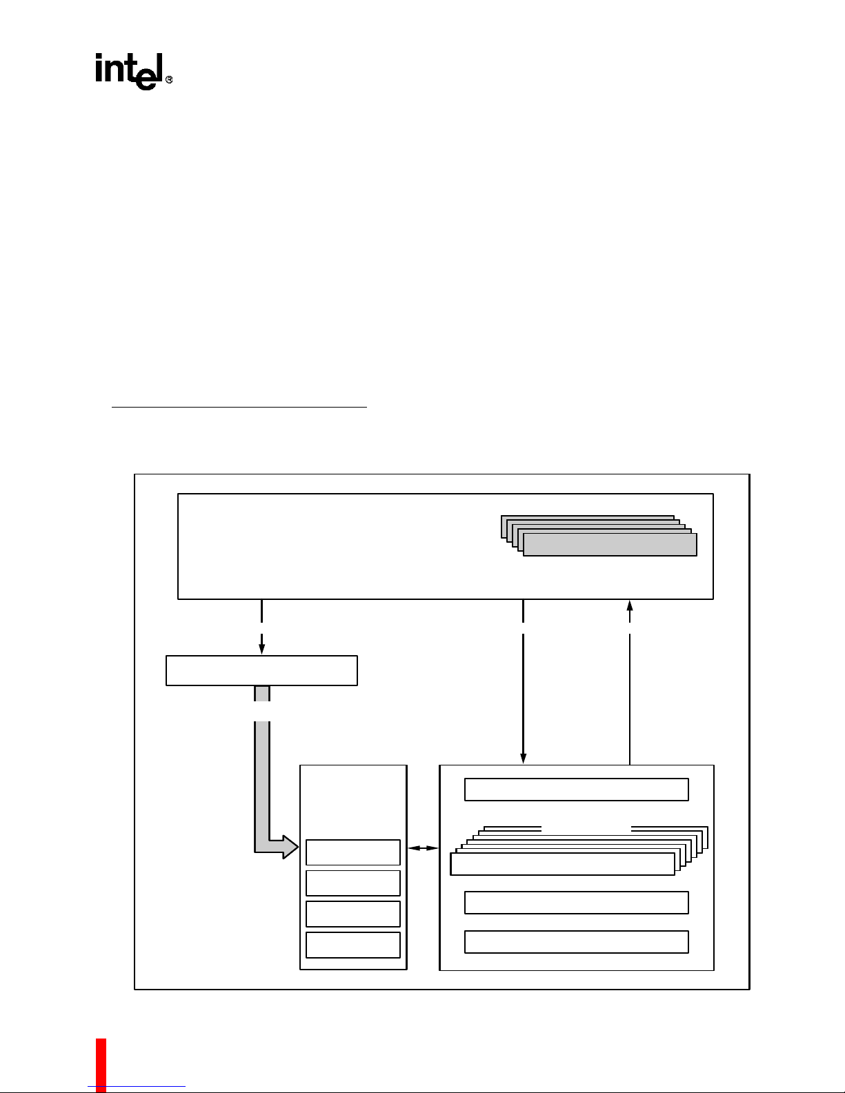
FFFF FFFFH0000 0000H
ADDRESS SPACE
ARCHITECTURALLY
DATA STRUCTURES
FETCH LOAD STORE
INSTRUCTION CACHE
INSTRUCTION
STREAM
INSTRUCTION
EXECUTION
PROCESSOR STATE
REGISTERS
INSTRUCTION
POINTER
ARITHMETIC
CONTROLS
PROCESS
CONTROLS
TRACE
CONTROLS
SIXTEEN 32-BIT GLOBAL REGISTERS
REGISTER CACHE
SIXTEEN 32-BIT LOCAL REGISTERS
FOUR 80-BIT FLOATING POINT REGISTERS
CONTROL REGISTERS
DEFINED
r15
g0
g15
r0
Figure 2. 80960KB Programming Environment
1
Page 8

80960KB
1.1 Key Performan ce Featu res
The 80 96 0 arc hitec tur e is b ased on the mos t rece nt
advances in microprocessor technology and is
grounded in Intel’s long experience in the design and
manufacture of embedded microprocessors. Many
features contribute to the 80960KB’s exceptional
performance:
1. Large Register Set. Having a la rge num be r of
registers reduces the number of times that a
processor needs to access memory. Modern
compilers can take advantage of this feat ure to
optimize execution speed. For maximum flexibility, the 80960KB provides thirty-two 32-bit
registers and four 80-bit floating point registers.
(See Figure 2.)
2. Fast I nstru ction Exe cution . Simpl e functi ons
make up the bulk of instructions in most
programs so that execution speed can be
improved by ensuring that these core instructions are ex ecut ed as quic kly as po ssib le. Th e
most frequently executed instructions such as
register-register moves, add/subtract, logical
operations and shifts execute in one to two
cycles. (Table 1 contains a list of instructions.)
3. Load/Store Architecture. One way to improve
execution speed is to reduce the number of
times that the processor must access memory
to perform an operation. As with other
processors based on RISC technology, the
80960KB has a Load/Store architecture. As
such, only the LOAD and STORE instructions
reference memory; all other instructions
operat e on registers. This type of architecture
simplifies instruction decoding and is used in
comb ination with other te chniqu es t o incre ase
para llelis m.
4. Simple Instruction Formats. All instructions
in the 8 0960KB are 32 bits long and m ust be
aligned on word boundaries. This alignment
makes it possible to eliminate the instruction
align ment stage in th e p ipeli ne. To simplif y the
instruction decoder, there are only five
instruction formats; each inst ruction uses only
one format. (See Figure 3.)
5. Overlapped Instruction Execution. Load
operations allow execution of subsequent
instructions to continue before the data has
been returned from memory, so that these
instructions can overlap the load. The
80960KB manages this process transparently
to software through the use of a register scoreboar d. Condi tional ins tructio ns also m ake use
of a scoreboard so that subsequent unrelated
instructions may be executed while the conditional instruction is pendin g.
6. Integer Execution Optimization. When the
resu lt of an a rith meti c ex ecu tion i s us ed a s an
operand in a subsequent calculation, the value
is se nt immedia tely to its dest ination register.
Yet at the same time, the value is put on a
bypass path to the ALU, thereby saving the
time that otherwise would be required to
retrieve the value for the next operation.
7. Bandwidth Optimizations. The 80960KB gets
optimal use of its memory bus bandwidth
because the bus is tuned for use with the
on-chip instruction cache: instruction cache
line size matches the maximum burst size for
instruction fetches. The 80960KB automatically
fetches four words in a burst and stores them
directly in the cache. Due to the size of the
cach e and the fa ct that i t is co ntin ua lly fi lled in
anticipation of needed instructions in the
prog ram flow, the 80960K B is rel atively insensitive to memory wait states. The benefit is that
the 80960KB delivers outstanding performance
even wi th a low cost memor y system.
8. Cache Bypass. If a cache miss occurs, the
processor fetches the needed instruction then
sends it on to the instruction decoder at the
same time it updates the cache. Thus, no extra
time is spent to load and read the cache.
2
Page 9

80960KB
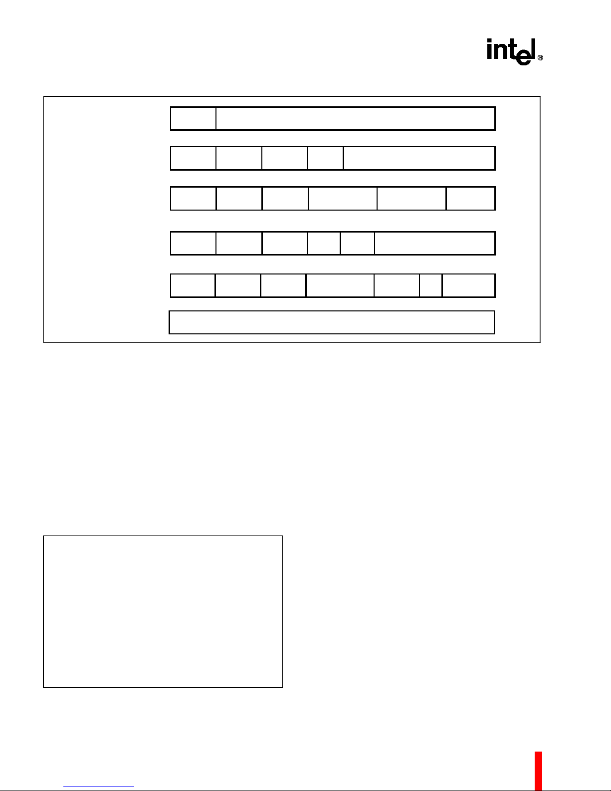
Table 1. 80960KB Instruction Set
Data Movement Arithmetic Logical Bit and Bit Field
Load
Store
Move
Load Address
Add
Subtract
Multiply
Divide
Remain der
Modulo
Shift
And
Not And
And Not
Or
Exclusive Or
Not Or
Or Not
Exclusive Nor
Not
Set Bit
Clear Bit
Not Bit
Check Bit
Alter Bit
Scan For Bit
Scan Over Bit
Extract
Modi fy
Nand
Rotate
Comp ar i son Branc h Call/Re t urn Fault
Compare
Conditional Compare
Com pa re an d Inc r e me nt
Com pa re and Decr em e nt
Unc on di tional Br an c h
Conditional Branch
Com pa re and Bran c h
Call
Call Extended
Call System
Return
Conditional Fault
Synchronize Faults
Bra nch and Link
Debug Miscellaneous Decimal Floating Point
Modify Trace Controls
Mark
Force Mark
Atomic Add
Atom i c Mo di fy
Flush Local Registers
Modify Arithmetic
Controls
Scan Byte for Equa l
Test Condition C ode
Modify Process Controls
Deci mal Move
Decimal Add with Carry
Decimal Subtract with
Carry
Move Real
Add
Subtract
Multiply
Divide
Remainder
Scale
Round
Square Root
Sine
Cosine
Tangent
Arctangent
Log
Log Binary
Log Natural
Exponent
Classify
Copy Real Extended
Compare
Synchronous Conversion
Synchronous Load
Synchronous Move
Convert Real to Integer
Convert Integer to Real
3
Page 10
80960KB
Control
Compare and
Branch
Register to
Register
Memory
Access—Short
Memory
Access—Long
OpcodeReg/LitRegMDisplacement
OpcodeRegReg/LitModesExt’d OpReg/Lit
OpcodeRegBaseModeScalexxOffset
Figure 3. Instruction Formats
1.1.1 Memory Space And Addressing Modes
The 80960KB offers a linear programming
environment so that all programs running on the
pro cessor are co ntaine d in a single add ress s pace.
Maximum address space size is 4 Gigabytes (2
32
bytes).
For ease of use the 80960KB has a small number of
addr ess ing mode s, bu t inc lude s al l th ose nece ssa ry
to ensure efficient execution of high-level languages
such as C. Table 2 lists the mode s.
Table 2. Memory Addressing Modes
• 12-Bit Offset
• 32-Bit Offset
• Register-Indirect
• Register + 12-Bit Offset
• Register + 32-Bit Offset
• Register + (Index-Register x Scale-Factor)
• Register x Scale Factor + 32-Bit Displacement
• Register + (Index-Register x Scale-Factor) +
32-Bit Displacement
• Scale-Facto r is 1, 2, 4, 8 or 16
OpcodeDisplacement
OpcodeRegBaseMXOffset
Displacement
1.1.2 Data Types
The 80960KB recognizes the following data types:
Numeric:
• 8-, 16-, 32- and 64-bit ordinals
• 8-, 16-, 32- and 64-bit integers
• 32-, 64- and 80-bit real numbers
Non-Numeric:
•Bit
• Bit Field
• Triple Word (96 bits)
• Quad-Word (128 bits)
1.1.3 Large Registe r Se t
The 8096 0KB pro gram ming en vironm ent inc ludes a
large number of registers. In fact, 32 registers are
available at any time. The availability of this many
registers greatly reduces the number of memory
accesses required to perform algorithms, which
leads to greater instruction processing speed.
There are two types of general-purpose registers:
local an d global. The 20 global registe rs consist of
sixteen 32-bit registers (G0 though G15) and four
80-bit registers (FP0 through FP3). These registers
4
Page 11

80960KB
perform the same function as the general-purpose
regi ste rs p r ov id ed i n other po pu la r m i croproc es so r s .
The term global refers to the fact that these registers
retain their contents across procedure calls.
The local registers, on the other hand, are procedure
specific. For each procedure call, the 80960KB
alloca tes 16 loca l regis ters ( R0 thr ough R1 5). Ea ch
local register is 32 bits wide. Any register can also be
used for single or double-precision floating-point
operations; the 80-bit floating-point registers are
provided for extended prec ision.
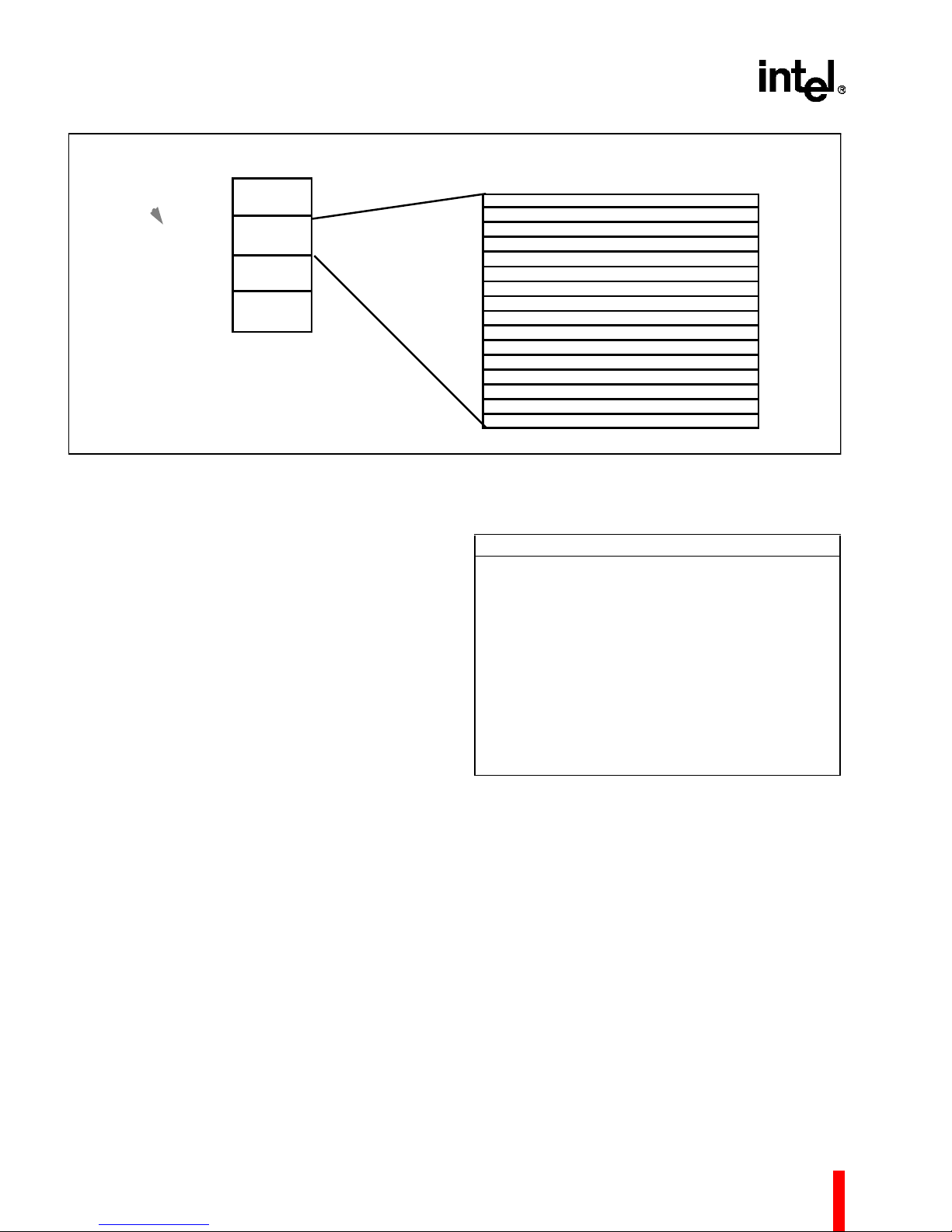
1.1.4 Multiple Register Sets
To further increase the efficiency of the register set,
multiple sets of local registers are stored on-chip
(See Figure 4). This cache holds up to four local
register frames, which means that up to three
procedure calls can be made without having to
access the procedure stack resident in memory.
Alth ough programs may have procedure calls nested
many calls deep, a program typically oscillates back
and forth between only two to three levels. As a
result, with four stack frames in the cache, the
probability of having a free frame available on the
cache when a c a ll is m ade is ve r y hi gh . In fact, runs
of representative C-language programs show that
80% of the calls are handled without needing to
access memory.
If four or more procedures are active and a new
proced ure is called, the 80960KB moves the oldest
local register set in the stack-frame cache to a
proc edure stac k in m emor y to make room fo r a new
set of registers. Global register G15 is the frame
pointer (FP) to the procedure stack.
Global and floating point registers are not
exchanged on a procedure call, but retain their
contents, making them available to all procedures for
fast parameter passing.
1.1.5 Instruction Cache
To further reduce memory accesses, the 80960KB
includes a 512-byte on-chip instruction cache. The
instruction cache is based on the concept of locality
of reference; most programs are not usually
executed in a steady stream but consist of many
branches, loops and procedure calls that lead to
jumping back and forth in the same small section of
code. Thus, by maintaining a block of instructions in
cache, the number of memory references required to
read instructions into the processor is greatly
reduced.
To load the instruction cache, instructions are
fetched in 16-byte blocks; up to four instructions can
be fetched at one time. An efficient prefetch
algorithm increases the probability that an instruction
will already be in the cache when it is needed.
Code for small loops often fits entirely within the
cache, leading to a great increase in processing
speed since further memory references might not be
neces s ary u nti l the program ex its the lo op. Sim il ar l y,
when calling short procedures, the code for the
calling procedure is likely to remain in the cache so it
will be there on the procedure’s return.
1.1.6 Register Sco reb oa rd ing
The instruction decoder is optimized in several ways.
One optimization method is the ability to overlap
instructions by using register scoreboarding.
Register scoreboarding occurs when a LOAD moves
a variable from memory into a register. When the
instruction initiates, a scoreboard bit on the target
register is set. Once the register is loaded, the bit is
reset. In between, any reference to the register
contents is accompanied by a test of the scoreboard
bit to ensure that the load has completed before
processing continues. Since the processor does not
need to wait for the LOAD to complete, it can
execute additional instructions placed between the
LOAD and the instruction that uses the register
contents, as shown in the following example:
ld data_2, r4
ld data_2, r5
Unrelated instruction
Unrelated instruction
add R4, R5, R6
In essence, the two unrelated instructions between
LOAD an d ADD are exe cu ted “f or f r ee ” ( i .e. , ta ke n o
apparent time to execute) because they are
executed while the register is being loaded. Up to
three load in structions can be pending at one tim e
with three corresponding scoreboard bits set. By
exploiting this feature, system programmers and
compiler writers have a useful tool for optimizing
exec ution speed.
5
Page 12
80960KB
REGISTER
ONE OF FOUR
LOCAL
REGISTER SETS
CACHE
Figure 4. Multiple Register Sets Are Stored On-Chip
1.1.7 Floating-Point Arithmetic
In the 80960KB, floating-point arithmetic has been
made an in teg r a l pa rt o f th e a rc hit ec tu r e. H avin g th e
floating-point unit integrated on-chip provides two
advantages. First, it improves the perform ance of the
chip for floating-point applications, since no
additional bus overhead is associated with
floating-point calculations, thereby leaving more time
for other bus operations such as I/O. Second, the
cost of using floating-point operations is reduced
because a separate coprocessor chip is not
required.
The 80960KB floating-point (real-number ) data types
include single-precision (32-bit), double-precision
(64-bit) and extended precision (80-bit) floating-point
numbers. Any registers may be used to execute
floating-point operations.
LOCAL REGISTER SET
R
0
R
15
31
0
Table 3. Sample Floating-Point Execution Times
(µs) at 25 MHz
Function 32-Bit 64-Bit
Add 0.4 0.5
Subtract 0.4 0.5
Multiply 0.7 1.3
Divide 1.3 2.9
Square Root 3.7 3.9
Arcta ng ent 10.1 13.1
Exponent 11.3 12.5
Sine 15.2 16.6
Cosine 15.2 16.6
1.1.8 High Bandwidth Local Bus
The processor provides hardware support for both
mandatory and recommended portions of IEEE
Standard 754 for floating-point arithmetic, including
all arithmetic, exponential, logarithmic and other
transcendental functions. Table 3 shows execution
times for some representative instructions.
6
The 80960KB CPU resides on a high-bandwidth
address/data bus known as the local bus (L-Bus).
The L-Bus provides a direct communication path
between the processor and the memory and I/O
subsystem interfaces. The processor uses the L-Bus
to fetch instructions, manipulate memory and
respond to interrupts. L-Bus features include:
• 32-bit mul tiplexed address/data path
• Four-word burst capability which allows transfers
from 1 to 16 byte s at a tim e
• High bandwidth reads and writes with
66.7 MBytes/s burst (at 25 MHz)
Tabl e 4 defines L-bu s signal names and functions;
Table 5 defines other component-support signals
such as interrupt lines.
Page 13

80960KB
1.1.9 Interrupt Handling
The 80960KB can be interrupted in two ways: by the
activa tion of on e o f fou r inter rup t pin s or b y se nding
a message on the processor’s data bus.
The 80960KB is unusual in that it automatically
handle s interr upts on a pr iority ba sis and can keep
track of pending interrupts through its on-chip
interr upt co ntroller. Two of the inte rrupt pi ns can be
configured to provide 8259A-style handshaking for
expansion beyond four interrupt lines.
1.1.10 Debug Features
The 8096 0KB has bui lt-in debug ca pabilitie s. There
are two types of breakpoints and six trace modes.
Debu g feature s are co ntroll ed by two internal 32-bi t
registers: the Process-Controls Word and the
Trace-Controls Word. By setting bits in these control
words, a software debug monitor can closely control
how the processor responds during program
execution.
The 80960KB provides two hardware breakpoint
registers on-chip which, by using a special
command, can be set to any value. When the
instr uction pointer matches either breakpoint register
value, the breakpoint handling routine is automatically called.
The 80960KB also provides software breakpoints
through the use of two instructions: MARK and
FMARK. These can be placed at any point in a
prog ram and cau se the proce ssor to halt execution
at that point and call the breakpoint handling routine.
The breakpoint mechanism is easy to use and
provides a powerful debugging tool.
Tracing is available for instructions (single step
execution), calls and returns and branching. Each
trace type may be enabled sepa rately by a spec ial
debug instruction. In each case, the 80960KB
executes the in struction firs t and then calls a trace
handling routine (usually part of a software debug
monitor). Further program execution is halted until
the routine completes, at which time execution
resumes at the next instruction. The 80960KB’s
tracing mechanisms, implemented completely in
hardware, greatly simplify the task of software test
and debug.
1.1.11 Fault Detection
The 80960KB has an automatic mechanism to
handle faults. Fault types include floating point, trace
and ar ith meti c fa ults. When t he p roces sor dete cts a
fault, it automatically calls the appropriate fault
handling routine and saves the current instruction
pointer and necessary state information to make
efficient recovery possible. Like interrupt handling
routines, fault handling routines are usually writ ten to
meet the needs of specific applications and are often
included as part of the operating system or kerne l.
For each of the fault types, there are numerous
subtypes that provide specific information about a
fault. For example, a floating point fault may have
the subtype set to an Overflow or Zero-Divide fault.
The fault handler can use this specific information to
respond correctly to the fault.
1.1.12 Built-in Testability
Upon re se t, the 80 960KB a ut om at ic ally c on du c ts a n
exhaustive internal test of its major blocks of logic.
Then, b efore ex ecutin g its firs t instru ction, it does a
zero check sum on the first eight words in memory to
ensure that the memory image was programmed
correctly. If a problem is discovered at any point
during the self-test, the 80960KB asserts its
FAILURE
pin an d will not beg in prog ram exe cution .
Self test takes approximately 47,000 cycles to
complete.
System manufacturers can use the 80960KB’s
self-test feature d uring incoming parts i nspection. No
special diagnostic programs need to be written. The
test is both thorough and fast. The self-t est capability
helps ensure that defective parts are discovered
before systems are shipped and, once in the field,
the self -test makes it ea sier to distingu ish between
prob lems cau sed b y pr oces sor fa ilur e an d prob le ms
resulting from other causes.
1.1.13 CHMOS
The 809 60KB is fabr icated using Intel’s CHMOS IV
(Complementary High Speed Metal Oxide Semiconductor ) pr oc ess. The 8 0960 KB is cu rre ntly avai labl e
in 16, 20 and 25 MHz versions.
7
Page 14
80960KB
Table 4. 80960KB Pin Description: L-Bus Signals (S heet 1 of 2)
NAME TYPE DESCRIPTION
CLK2 I SYSTEM CLOCK provides the fundamental timing for 80960KB systems. It is
divided by two inside the 80960KB and four 80-bit registers (FP0 through FP3) to
generate the internal processor clock.
LAD31:0 I/O
T.S.
LOCAL ADDRESS / DATA BUS carries 32-bit physical addresses and data to
and from memory. During an address (T
address (bits 0-1 indicate SIZE; see below). Dur ing a data (T
) cycle, bits 2-31 contain a physical word
a
) cycle, bits 0-31
d
contain read or write data. These pins float to a high impe dance state when not
active.
Bits 0-1 comprise SIZE during a T
cycle. SIZE specifies burst transfer size in
a
words.
LAD1 LAD0
00 1 Word
0 1 2 Words
1 0 3 Words
1 1 4 Words
ALE
ADS
W/R
DT/R
DEN
READY
LOCK
O
T.S.
O
O.D.
O
O.D.
O
O.D.
O
O.D.
I READY indicates that data on LAD lines can be sampled or removed. If READY
I/O
O.D.
ADDRESS LATCH ENABLE indicates the transfer of a physical address. ALE is
asserted during a T
cycle and deasserted before the beginning of the Td state. It
a
is activ e LO W an d flo at s to a hig h im pe dance st ate dur i ng a hold cyc le (T
ADDRESS/DATA STATUS indicates an address state. ADS is asserted every Ta
state an d dea ss er ted du rin g t h e fol l owi ng T
asserted again every T
state where READY was asserted in the previous cycle.
d
state . Fo r a b ur st t r ansa ct ion, A DS is
d
WRITE/READ specifies, during a Ta cycle, whether th e operation is a writ e or
read. It is latched on-chip and r emains valid during T
cycles.
d
DATA TRANSMIT / RECEIVE indicates the direction of data transfer to and from
the L-Bus. It is low during T
edgm ent; it is hi gh during T
when DEN
is asserted.
and Td cycles for a read or interr upt acknowl-
a
and Td cycles for a write. DT/R neve r ch an ges state
a
DATA ENABLE (active low) enables data transceivers. The processor asserts
DEN# during all Td and Tw states. The DEN# line is an open drain-output of the
80960KB-processor.
is not asserted during a T
inserting a wait state (T
cycle, the Td cycle is extended to the next cycle by
d
) and ADS is not asserted in the next cycle.
w
BUS LOCK prevents bus masters from gaining control of the L-Bus during
Read/Modify/Write (RMW) cycle s. The processor or any bus agent may assert
LOCK
.
At t he start of a RMW operat ion, the processor examines the LOCK
pin. If the pin
is already asserted, the processor waits until it is not asserted. If the pin is not
asser te d, th e p roce ss or ass ert s LO CK
The processor deasserts LOCK
time LOCK
is asserted, a bus agent can perform a normal read or write but not a
in the Ta cycle of the write transaction. During th e
during the Ta cycle of the read transaction.
RMW op eration.
The processor also asserts LOCK
Do not leave LOCK
unconnected. It must be pulled high for the processor to
during interrupt-acknowledge transactions.
function properly.
I/O = Input/Output, O = Output, I = Input, O.D. = Open Drain, T .S. = Three-state
).
h
ERRATA - 6/13/97
pin description omitted.
DEN
8
Page 15

80960KB
Table 4. 80960KB Pin Description: L-Bus Signals (She et 2 of 2)
NAME TYPE DESCRIPTION
BE3:0 O
O.D.
BYTE ENABLE LINES specify the data bytes (up to four) on the bus which are
used in th e c urr e nt bu s c ycl e. BE 3
corresponds to LAD31:24; BE0 corresponds to
LAD7:0.
The byte enables are provided in advance of data:
Byte enables asserted during T
Byte enables asserted during T
(the word to be transmitted following the next assertion of READY
Byte enables that occur during T
READY
from one T
are undefined. Byte enables are latched on-chip and remain constant
cycle to the next when READY is not asserted.
d
specify the bytes of the first data word.
a
specify the bytes of the next data word, if any
d
).
cycles that precede the last assertion of
d
For reads, byte enables specify the byte(s) that the processor will actually use.
L-Bus agents are required to assert only adjacent byte enables (e.g., asserting
just BE0
enable. Address bi ts A
and BE2 is not permitted) and are required to assert at least one byte
and A1 can be decoded externally from the byte enables.
0
HOLD I HOLD: A request fro m an external bus master to acquire the bus. When the
processor receives HOLD and grants bus control to another master, it floats its
three-state bus lines and open-drain control lines, asserts HLDA and enters the
T
state. When HOLD deasserts, the processor deasserts HLDA and enters the
h
or Ta state.
T
i
HLDA O
T.S.
CACHE O
T.S.
HOLD ACKNOWLEDGE: Notifies an external bus master that the processor has
relinquished control of the bus.
CACHE indicates when an access is cacheable during a T
cycle. It is not
a
asserted during any synchronous access, such as a syn c hronous load or move
instruction used for sending an IAC message. Th e CACHE s ignal floats to a high
impedance state when the processor is idle.
I/O = Input/Output, O = Output, I = Input, O.D. = Open Drain, T.S. = Three-state
Table 5. 80960KB Pin Description: Support Signals (Sheet 1 of 2)
NAME TYPE DESCRIPTION
BADAC
I BAD ACCESS, if asserted in the cycle following the one in which the last READY
of a tr ansaction is asserted, indicates that an unre coverable error has occurred
on the c urr ent bu s tr an sa ctio n or t ha t a syn ch ron ous l oad/ st ore i nstr uct io n h as not
been acknowledged.
During system reset the BADAC
signal is interpreted differently. If the signal is
high, it indicates that t his processor will perform system initialization. If it is low,
another processor in the system will perform system initialization instead.
RESET I RESET clears the processor’s internal logic and causes it to reinitialize.
During RESET assertion, the input pins are ignored (except for BADAC
/INT0), the three-state output pins are placed in a high impedance state and
IAC
other output pins are placed in their non-asserted states.
RESET must be asserted for at least 41 CLK2 cycl es for a predictabl e RESET.
The HIGH to LOW transition of RESET should occur after the rising edge of both
CLK2 and the external bus clock and before the next rising edge of CLK2.
I/O = Input/Output, O = Output, I = Input, O.D. = Open Drain, T .S. = Three-state
and
9
Page 16

80960KB
Table 5. 80960KB Pin Description: Support Signals (Sheet 2 of 2)
NAME TYPE DESCRIPTION
FAILURE O
O.D.
INITIALIZATION FAILURE indicates that the processor did not initialize correctly .
After R ESET deassert s and before the first bus transaction begins, FAI LURE
asserts while the processor performs a self-test. If the self-test completes
successfully, then FAILURE
checksum on the first eight words of memory. If it fails, FAILURE
deasserts. The processor then perform s a zero
assert s for a
second time and remains asserted. If it passes, system initiali zation contin ues
IAC
/INT
and FAILURE
0
I INTERAGENT COMMUNICATION REQUEST/INTERRUPT 0 indicates an IAC
remains deasserted.
messag e or an interr upt is pendi ng. The bus interrupt co ntrol regist er determines
how the signal is interpreted. To signal an interrupt or IAC request in a
synchronous system, this pin — as well as the other interrupt pins — must be
enabled by being deasserted for at least one bus cycle and then asserted for at
least one additional bus cycle. In an asynchronous system the pin must remain
deasserted for at least two bus cycles and then asserted for at least two more bus
cycles.
During system reset, this signal must be in the logic high condition to enable
normal processor operation. The logic low conditi on is reserved.
INT
1
/INTR I INTERRUPT2/INTERRUPT REQUEST: The interrupt control regist er determines
INT
2
I INTERRUPT 1, like INT0, provides direct interrupt signaling.
how this pin is interpreted. If INT
INT
pins. If INTR, it is used to receive an interrupt request from an external
1
, it has the same interpretation as the INT0 and
2
interrupt controller.
/INTA I/O
INT
3
O.D.
INTERRUPT3/INTERRUPT ACKNOWLEDGE: The bus interrupt control register
determines how this pin is interpreted. If INT
the INT
, INT1 and INT2 pins. If INT A, it is used as an output to control
0
inter ru pt-ack no w le dg e tr an s ac tio ns . The IN TA
remains valid during T
cycles; as an output, it is open-drain.
d
, it has the same interpretation as
3
output is latched on-chip and
N.C. N/A NOT CONNECTED indicates pins should not be connected. Never connect any
pin marked N.C. as thes e pins may be reserved for fact ory use.
I/O = Input/Output, O = Output, I = Input, O.D. = Open Drain, T.S. = Three-state
2.0 ELECTRICAL SPECIFICATIONS
2.1 Power and Grounding
The 80960KB is implemented in CHMOS IV
technology and therefore has modest power requirements. Its high clock frequency and numerous
output buffers (address/data, control, error and
arbitration signals) can cause power surges as
multiple output buffers simultaneously drive new
signal levels. For clean on-chip power distribution,
V
and VSS pins separately feed the device’s
CC
functional units. Power and ground connections
10
must be made to all 80960KB power and ground
pins. On the circuit board, all V
pins must be
cc
strapped closely together, preferably on a power
plane; all V
pins should be strapped together,
ss
preferably on a ground plane.
2.2 Power Decoupling
Recommendations
Place a liberal amount of decoupling capacitance
near the 80960KB. When driving the L-bus the
processor can cause transient power surges, particularly when connected to a large capacitive load.
Page 17

Low inductance capacitors and interconnects are
recommended for best high frequency electrical
performance. Inductance is reduced by shortening
board traces between the processor and decoupling
capacitors as much as possible.
2.3 Connection Recomm endatio ns
OPEN-DRAIN OUTPUT
80960KB
V
CC
180 Ω
For reliable operat ion, always connect unused inputs
to an appropriate signal level. In particular, if one or
more interrupt lines are not used, they should be
pulled up. No inputs should ever be left floating.
All open-drain outputs require a pullup device. While
in most cases a simple pullup resistor is adequate, a
netwo rk o f p ul lu p and pu lldown r es is tors biased t o a
valid V
(>3.0 V) and terminated in the characteristic
IH
impedance of the circuit board is recommended to
limit noise and AC power consumption. Figure 5 and
Figure 6 show recommended values for the resistor
network for low and high current drive, assuming a
characteristic impedance of 100
Ω. Terminating
output si gnal s in this fashi on li mits sig nal s win g and
reduces AC power consumption.
NOTE: Do not connect external logic to pins marked
N.C.
V
CC
OPEN-DRAIN OUTPUT
220 Ω
High Drive Network:
= 3.4 V
V
OH
= 25.3 mA
I
OL
390 Ω
Figure 6. Connection Recommendations
for High Current Drive Network
2.4 Characteristic Curves
Figure 7 shows typical supply current requirements
over the operating temperature range of the
processor at supply voltage (V
and Figure 9 show the typical power supply current
(I
) that th e 8 09 60KB re quires at var io us o pe r at in g
CC
frequencies when measured at three input voltage
(V
) levels an d t wo temperatur es .
CC
For a given outpu t current (I
10 shows the worst case output low voltage (V
Figure 11 shows the typical capacitive derating
curve f or the 80 960KB me asured fr om 1.5V on the
syste m cloc k (CLK ) to 1.5V o n the fa lling e dge an d
1.5V on the rising edge of the L-Bus address/data
(LAD) signals.
) of 5 V. Figure 8
CC
) the cu rve in Figur e
OL
OL
).
Low Drive Network:
= 3.0 V
V
OH
= 20.7 mA
I
OL
Figure 5. Connection Recommendations
for Low Current Drive Network
330 Ω
11
Page 18

80960KB
VCC = 5.0 V
380
360
340
320
25 MHz
20 MHz
16 MHz
300
280
260
240
POWER SUPPLY CURRENT (mA)
220
200
-60-40-20020406080100120140
CASE TEMPERATURE (°C)
Figure 7. Typical Supply Current vs. Case Temperature
TEMP = +22°C
@5.5V
@5.0V
@4.5V
Figure 8. Typical Current vs. Frequency (Room Temp)
400
380
360
340
320
300
280
260
240
TYPICAL SUPPLY CURRENT (mA)
220
200
180
16 20 25
OPERATING FREQUENCY (MHz)
12
Page 19

80960KB
TEMP = +22°C
@5.5V
@5.0V
@4.5V
Figure 9. Typical Current vs. Frequency (Hot Temp)
380
360
340
320
300
280
260
240
220
TYPICAL SUPPLY CURRENT (mA)
200
180
160
16 20 25
OPERATING FREQUENCY (MHz)
(TEMP = +85°C, V
CC
= 4.5V)
0.8
0.6
0.4
0.2
0.0
01020304050
OUTPUT LOW VOLTAGE (V)
OUTPUT LOW CURRENT(mA)
Figure 10. Worst-Case Voltage vs. Output
Current on Open-Drain Pins
2.5 Test Load Circui t
Figure 12 illustr ates th e load ci rcuit us ed to test the
(TEMP = +85°C, V
CC
= 4.5V)
30
FALLING
25
20
15
10
VALID DELAY(ns)
5
THREE-STATE OUTPUT
RISING
0
020406080100
CAPACITIVE LOAD(pF)
Figure 11. Capacitive Derating Curve
80960K B’s three-state pins; Figure 13 shows the
load ci rcuit us ed to test the o pen d rain ou tputs . The
open drain test uses an active load circuit in the form
13
Page 20

80960KB
of a matched diode bridge. Since the open-drain
outputs sink current, only the I
are necessary and the I
legs are not used. W hen
OH
legs of the bridg e
OL
the 80960KB driver under test is turned off, the
outpu t pin is pu lled up to V
(i.e., VOH). Diode D
REF
is turned off and the IOL current source flows through
diode D
.
2
THREE-STATE OUTPUT
1
C
L
When the 80960KB open-drain driver under test is
on, diode D
being tested drops to V
is a lso on a nd the v oltage on the pin
1
. Diode D2 turns off and I
OL
OL
flows through diode D1.
C
= 50 pF for all signals
L
Figure 12. Test Load Circuit for Three-State
Output Pins
I
OL
OPEN-DRAIN OUTPUT
= V
CC
D
2
C
L
CL = 50 pF for all signals
D
1
IOL Tested at 25 mA
V
REF
D1 and D2 are matched
Figure 13. Test Load Circuit for Open-Drain
Output Pins
14
Page 21
80960KB
2.6 Absolute Maximum R atings
Operating Temperature(PGA)................... 0°C to +85°C Case
(PQFP)............. 0°C to +100°C Case
Storage Temperature.................................... –65°C to +150°C
Voltage on Any Pin .................................. –0.5V to VCC +0.5V
Power Dissipation............................................ 2.5W (25 MHz)
NOTICE:This is a production data sheet. The specifi-
cations are subject to change without notice.
*WARNING: Stressing the dev ice beyond th e
“Absolute Maximum Ratings” ma y cause
permanent damage. These are stress ratings
only. Operation beyond the “Operating Conditions” is not recommended and extended
exposu re be yond the “Opera ting C ondit ions ” may
affect device reliability.
2.7 DC Characteristics
PGA: 80960KB (16 MHz) T
80960KB (20 and 25 MHz) T
PQFP: 80960KB (16 MHz) T
80960KB (20 and 25 MHz) T
Symbol Parame t er Min Max Units Notes
V
IL
V
IH
V
CL
V
CH
V
OL
V
OH
I
CC
Input Low Voltage –0.3 +0.8 V
Input High Voltage 2.0 VCC + 0.3 V
CLK2 Input Low Voltage –0.3 +0.8 V
CLK2 Input High Voltage 0.55 V
Output Low Voltage 0.45 V (1,2)
Output High Voltage 2.4 V (3,4)
Power Supply Current:
16 MHz
20 MHz
25 MHz
I
LI
I
LO
C
IN
C
O
C
CLK
NOTES:
1. For three-state outputs, this parameter is measured at:
Address/Data ........................................ 4.0 mA
Controls.................................................. 5.0 mA
2. For open-drain outputs ........................... 25 mA
3. This parameter is measured at:
Address/Data ...................................... -1.0 mA
Controls................................................ -0.9 mA
ALE
4. Not measured on open-drain outputs.
5. Measured at worst case frequency, V
in Figures 12 and 13. Figure 7, Figure 8 and Figure 9 indicate typical values.
6. Input, output and clock capacitance are not tested.
Input Leakage Current ±15 µA 0 ≤ VIN ≤ V
Output Leakage Current ±15 µA 0.45 ≤ VO ≤ V
Input Capacitance 10 pF fC = 1 MHz (6)
Output Capacitance 12 pF fC = 1 MHz (6)
Clock Capacitance 10 pF fC = 1 MHz (6)
..................................................... -5.0 mA
= 0°C to +85°C, VCC = 5V ± 10%
CASE
= 0°C to +85°C, VCC = 5V ± 5%
CASE
= 0°C to +100°C, VCC = 5V ± 10%
CASE
= 0°C to +100°C, VCC = 5V ± 5%
CASE
Table 6. DC Ch aracteristics
CC
and temperature, with device operating and outputs loaded to the test conditions
CC
VCC + 0.3 V
315
360
420
mA
mA
mA
(5)
(5)
(5)
CC
CC
15
Page 22

80960KB
2.8 AC Specifications
This sect ion des cribes the AC specif icatio ns for th e
80960KB pins. All input and output timings are
spec ifi ed r el ati ve to th e 1 .5 V level of the rising edg e
of CL K2. For outp ut timings the specific ations re fer
to the time it takes the signal to reach 1.5 V.
EDGE
CLK2
0.8V
OUTPUTS:
LAD 31:0
ADS
W/R, DEN
BE3:0
HLDA
CACHE
LOCK, INTA
ABC
1.5V
T
T
8
1.5V 1.5V 1.5V
6
1.5V
VALID OUTPUT
T
8
T
13
For input timings the specifications refer to the time
at which the signal reaches (for input setup) or
leaves (for hold time) the TTL levels of LOW (0.8 V)
or HIGH (2.0 V). All AC testing should be done with
input voltages of 0.4 V and 2.4 V, except for the
clock (CLK2), which should be tested with input
voltages of 0.45 V and 0.55 V
D
A
T
9
1.5V
BC
T
14
CC
.
ALE
DT/R
INPUTS:
LAD31:0
BADAC
IAC/INT0, INT1
INT2/INTR, INT3
HOLD
LOCK
READY
1.5V
1.5V
T
7
T
6
10
12
VALID OUT PUT
T
11
T
11
1.5V 1.5V
T
2.0V 2.0V
0.8V 0.8V
T
2.0V 2.0V
0.8V 0.8V
VALID INPUT
T
9
Figure 14. Drive Levels and Timing Relationships for 80960KB Signals
16
Page 23

2.8.1 AC Specification Tables
Table 7. 80960KB AC Characteristics (16 MHz)
Symbol Parameter Min M ax Units Notes
Input Clock
80960KB
T
T
T
T
T
Pro cessor Clock Pe riod (CLK2) 31.25 125 ns VIN = 1.5V
1
Pro cessor Clock Low Time (CLK2) 8 ns VIL = 10% Point = 1.2V
2
Processor Clock High Time (CLK2) 8 ns VIH = 90% Point = 0.1V + 0.5 V
3
Pro cessor Clock Fall Time (CLK2) 10 ns VIN = 90% Point to 10% Point (1)
4
Pro cessor Clock R ise Time (C LK2) 10 ns VIN = 10% Point to 90% Point (1)
5
CC
Synch r on ou s O utp uts
T
T
T
T
T
T
Output Valid Delay 2 25 ns
6
HLDA Output Valid Delay 4 28 ns
6H
ALE Width 15 ns
7
ALE Output Valid Delay 2 18 ns
8
Output Float Delay 2 20 ns (2)
9
HLDA Output Float Delay 4 20 ns (2)
9H
Synchron ou s Inp uts
T
T
Input Setup 1 3 ns (3)
10
Input Hold 5 ns (3)
11
T
11H
T
T
T
T
T
T
NOTES:
1. Clock rise and fall times are not tested.
2. A float condition occurs when the maximum output current becomes less than I
should not be longer than the valid delay .
3. LAD31:0, BADAC
chronous or asynchronous.
HOLD Input Hold 4 ns (3)
Input Setup 2 8 ns (3)
12
Setup to ALE Inactive 10 ns
13
Hold after ALE Inac tiv e 8 ns
14
Reset Hold 3 ns (3)
15
Reset Setup 5 ns (3)
16
Reset Width 1281 ns 41 CL K2 Per i od s Mini m um
17
, HOLD, LOCK and READY are synchronous inputs. IAC/INT0, INT1, INT2/INTR and INT3 may be syn-
. Float delay is not tested; however, it
LO
17
Page 24

80960KB
Table 8. 80960 KB AC Characteristics (20 MHz)
Symbol Parameter Min Max Units Notes
Input Clock
T
T
T
T
T
Processor Clock Peri od (CLK2) 25 125 ns VIN = 1.5V
1
Processor Clock Low Time (CLK2) 6 ns VIL = 10% Point = 1.2V
2
Processor Clock High Time ( CLK2) 6 ns VIH = 90% Point = 0.1V + 0.5 V
3
Processor Clock Fall Time (CLK2) 10 ns VIN = 90% Point to 10% Poi nt (1)
4
Processor Clock Rise Time (CLK2) 10 ns VIN = 10% Point to 90% Poi nt (1)
5
CC
Synchronous Outputs
T
T
T
T
T
T
Output Valid Delay 2 20 ns
6
HLDA Output Valid Delay 4 23 ns
6H
ALE Width 12 ns
7
ALE Output Valid Delay 2 18 ns
8
Outp ut Float Delay 2 20 ns (2)
9
HLDA Output Float Delay 4 20 ns (2)
9H
Synchr onous Inputs
T
T
Input Setup 1 3 ns (3)
10
Input Hold 5 ns (3)
11
T
11H
T
T
T
T
T
T
NOTES:
1. Clock rise and fall times are not tested.
2. A float condition occurs when the maximum output current becomes less than I
should not be longer than the valid delay.
3. LAD31:0, BADAC
chronous or asynchronous.
HOLD Input Hold 4 ns (3)
Input Setup 2 7 ns (3)
12
Setup to ALE Inac tiv e 10 ns
13
Hold after ALE Inactive 8 ns
14
Reset Hold 3 ns
15
Reset Setup 5 ns
16
Reset Width 1025 ns 41 CLK2 Periods Minimum
17
, HOLD, LOCK and READY are synchronous inputs. IAC/INT0, INT1, INT2/INTR and INT3 may be syn-
. Float delay is not tested; however, it
LO
18
Page 25

Table 9. 80960KB AC Characteristics (25 MHz)
Symbol Parameter Min Max Units Notes
Input Clock
80960KB
T
T
T
T
T
Pro cessor Clock Pe riod (CLK2) 20 125 ns VIN = 1.5V
1
Pro cessor Clock Low Time (CLK2) 5 ns VIL = 10% Point = 1.2V
2
Processor Clock High Time (CLK2) 5 ns VIH = 90% Point = 0.1V + 0.5 V
3
Pro cessor Clock Fall Time (CLK2) 10 ns VIN = 90% Point to 10% Point (1)
4
Pro cessor Clock R ise Time (C LK2) 10 ns VIN = 10% Point to 90% Point (1)
5
CC
Synch r on ou s O utp uts
T
T
T
T
T
T
Output Valid Delay 2 18 ns
6
HLDA Output Valid Delay 4 23 ns
6H
ALE Width 12 ns
7
ALE Output Valid Delay 2 18 ns
8
Output Float Delay 2 18 ns (2)
9
HLDA Output Float Delay 4 20 ns (2)
9H
Synchron ou s Inp uts
T
T
Input Setup 1 3 ns (3)
10
Input Hold 5 ns (3)
11
T
11H
T
T
T
T
T
T
NOTES:
1. Clock rise and fall times are not tested.
2. A float condition occurs when the maximum output current becomes less than I
should not be longer than the valid delay .
3. LAD31:0, BADAC
chronous or asynchronous.
HOLD Input Hold 4 ns
Input Setup 2 7 ns
12
Setup to ALE Inactive 8 ns
13
Hold after ALE Inac tiv e 8 ns
14
Reset Hold 3 ns
15
Reset Setup 5 ns
16
Reset Width 820 ns 41 CL K2 Per i od s Mini m um
17
, HOLD, LOCK and READY are synchronous inputs. IAC/INT0, INT1, INT2/INTR and INT3 may be syn-
. Float delay is not tested; however, it
LO
19
Page 26

80960KB
T
1
T
3
HIGH LEVEL (MIN) 0.55V
LOW LEVEL (MAX) 0.8V
CLK2
CLK
1.5 V
10%
90%
T
4
FIRST
ABCDA
CC
T
5
Figure 15. Processor Clock Pulse (CLK2)
...
...
T
2
...
RESET
T
OUTPUTS
INIT PARAMETERS (BADAC
/IAC) MUST BE SET UP 8 CLOCKS
INT
0
PRIOR TO THIS CLK2 EDGE
INIT PARAMETERS MUST BE HELD
BEYOND THIS CLK2 EDGE
...
,
Figure 16. RESET Signal Timing
T
15T16
17
T15 = RESET HOLD
T
= RESET SETUP
16
= RESET WIDTH
T
17
20
Page 27

80960KB
3.0 MECHANICAL DATA
3.1 Packaging
The 80960KB i s available i n two package types:
• 132-lead ceramic pin-grid array (PGA). Pins are
arra nged 0. 10 0 inc h ( 2.5 4 mm ) cen ter -t o-ce nt er, in
a 14 by 14 matrix, three rows around (see Figure
17).
• 132-lead plastic quad flat pack (PQFP). This
package uses fine-pitch gull wing leads arranged
in a single row along the package perimeter with
0.025 inch (0.64 mm) spacing (see Figure 20).
Dime nsio ns f or bo th pack age type s ar e giv en i n the
Intel
Packaging
handbook (Order #240800).
1
2
3
4
5
6
7
8
9
10
11
12
13
14
3.1.1 Pin Assignment
The PGA and PQFP have different pin assignments.
Figure 18 shows the view from the PGA bottom (pins
facing up) and Figure 19 shows a view from the PGA
top (p ins facin g down). F igure 20 shows the P QFP
package; Figure 21 shows the PQFP pinout with
signal names. Notice that the pins are numbered in
order from 1 to 132 around the package perimeter.
Table 10 and Table 11 list the function of each PGA
pin; Table 12 and Table 13 lis t the functio n of each
PQFP pin.
ABCDEFGHJK LMNP
Figure 17. 132-Lead Pin-Grid Array (PGA) Package
21
Page 28

80960KB
1413121110987654321
P
CC
N.C.N.C.N.C.N.C.N.C.N.C.N.C.N.C.N.C.N.C.N.C.V
SS
CC
V
V
N
SS
N.C.N.C.N.C.N.C.N.C.N.C.N.C.N.C.N.C.N.C.N.C.N.C.N.C.V
M
N.C.
V
V
SS
CC
V
V
CC
SS
N.C.N.C.N.C.N.C.
V
V
SS
CC
N.C.N.C.N.C.
L
V
N.C.DEN
CC
V
SS
N.C.N.C.
K
V
FAILBE
3
SS
V
CC
N.C.N.C.
J
DT/R
BE
V
SS
2
N.C.N.C.N.C.
H
W/R
LOCKBE
0
N.C.N.C.N.C.
G
READYLAD
30
BE
1
N.C.N.C.N.C.
F
LAD
31
29
N.C.N.C.N.C.
CACHE
LAD
E
LAD
28
LAD
LAD
27
26
N.C.N.C.
V
SS
D
HLDAADSALE
V
CC
N.C.N.C.
C
V
BADACHOLD LAD
25
V
CC
LAD
SS
LAD
20
13
LAD
LAD
3
8
V
V
CC
SS
INT
3
INT
INT
0
1
B
LAD
LAD
23
22
24
18
21
12
15
6
10
2
CLK2
LAD
LAD
LAD
LAD
LAD
LAD
LAD
LAD
RESETLAD
0
V
SS
A
V
CC
19
SS
LAD
17
16
LAD
LAD
V
LAD
LAD
LAD
11
14
9
LAD
LAD
5
7
LAD
LAD
1
4
INT
V
CC
2
P
N
M
L
K
J
H
G
F
E
D
C
B
A
Figure 18. 80960KB PGA Pinout—View from Bottom (Pins Facing Up)
ERRATA
6-17-97:
Pin M2 was N.C.; should be V
Pin M13 was V
This page now shows it correctly.
22
; should be N.C.
CC
CC
1413121110987654321
.
Page 29

14 13 12 11 10 9 8 7 6 5 4 3 2 1
80960KB
P
N
M
L
K
J
H
G
F
E
D
C
B
A
VCCVSSN.C. N.C. N.C. N.C. N.C. N.C. N.C. N.C. N.C. N.C. N.C. V
N.C. N.C.
V
CCVSS
N.C.
V
SS
VCCN.C. DEN
VSSFAIL BE
VSSBE2DT/R
VCCN.C.
N.C. N.C. N.C. N.C. N.C. N.C. N.C. N.C. N.C. N.C.
N.C. N.C. N.C.
N.C. N.C.
N.C. N.C.
N.C. N.C. N.C.
V
CCVSS
V
SS
V
CC
N.C. N.C. N.C. N.C.
2
BK06
N.C. N.C. N.C.
N.C. N.C. N.C.
N.C. N.C. N.C.
V
N.C. N.C.
SS
N.C. N.C.
INT0INT1INT
V
SS
VCCINT
14 13 12 11 10 9 8 7 6 5 4 3 2 1
V
CC
V
V
SS
3
RESET LAD
CLK2
0
LAD1LAD4LAD5LAD7LAD9LAD11LAD14LAD16LAD17LAD
2
LAD3LAD
CC
LAD2LAD6LAD10LAD12LAD15LAD18LAD21LAD22LAD24LAD
X
X
X
X
XXXX
XX
XX
90
XXX
XXX
8
x 5
X
X
V
LAD
LAD
8
20
13
V
SS
CC
LOCK BE0W/R
BE1READY LAD
CACHE LA D31LAD
LAD27LAD26LAD
HLDA ADS ALE
BADAC HOLDLAD
19
25
VSSV
CC
V
SS
3
CC
P
N
M
L
K
J
H
G
30
F
29
E
28
D
C
B
23
A
Figure 19. 80960KB PGA Pinout—View from Top (Pins Facing Down)
Fi
gure 20. 80960KB 132-Lead Plastic Quad Flat-Pack (PQFP) Package
NOTE: To address the fact that many of the package prefix variables have changed,
all package prefix variables in this document are now indicated with an "x".
23
Page 30

80960KB
LAD0
LAD1
LAD2
V
LAD3
LAD4
LAD5
LAD6
LAD7
LAD8
LAD9
LAD10
LAD11
LAD12
V
LAD13
LAD14
LAD15
LAD16
LAD17
LAD18
LAD19
LAD20
LAD21
LAD22
V
LAD23
LAD24
LAD25
BADAC
HOLD
NC
ADS
RT
A
0TNI/
TESE
S
CN
CNCNCNC
S
V
99 9 8 97
100
101
102
103
SS
104
105
106
107
108
109
110
11
112
113
114
SS
115
116
117
118
119
120
121
122
123
124
125
SS
126
127
128
129
130
131
132
96 95 9 4 93 92 91 90 89 8 8 87 86 85 84 8 3 8 2 81 80 79 7 8 77 76 75 74 73 7 2 71 70 6 9 68 67
1
1 2 3
4 5 6 7 8 9 1 0 11 12 13 14 15 16 1 7 18 1 9 2 0 21 2 2 23 24 25 26 2 7 28 29 3 0 31 32 33
CC
N
V
R
TNI/
2KLC
NI/2
3
1T
C
S
CC
S
T
T
C
S
V
N
C
S
N
NI
NI
AI
V
I
SS
S
CNCNCN
C
CN
C
V
S
V
V
V
C
N
N
B
XXX
K0
6908
x 52
X
XXX
X
XXXXXX
XXX
XX
X
CC
C
SS
C
C
V
N
V
V
VCCV
S
S
S
S
V
NC
66
NC
65
64
NC
NC
63
62
NC
61
NC
60
NC
59
NC
58
NC
V
57
56
55
54
53
52
51
50
49
48
47
46
45
44
43
42
41
40
39
38
37
36
35
34
V
V
NC
V
V
NC
NC
NC
NC
NC
NC
NC
NC
NC
V
V
NC
NC
NC
NC
V
V
NC
SS
CC
CC
SS
SS
SS
CC
CC
CC
6
7
A
EL
2
2
DL
D
D
A
A
A
H
L
L
NOTE: To address the fact that many of the package prefix variables have changed,
all package prefix variables in this document are now indicated with an "x".
24
2DAL
DAL
H
V
D
C
A
A
L
C
S
9
0
8
1
E
S
2
3
3DAL
0
1
Y
R/TD
R
/W
E
E
D
B
B
AER
S
2
3
E
E
E
R
B
B
UL
I
AF
S
N
K
S
S
E
CO
V
V
D
L
Figure 21. PQFP Pinout - View From Top
S
S
S
CN
C
S
N
V
C
S
S
N
V
V
S
C
C
V
S
C
C
S
S
C
N
V
V
V
Page 31

3.2 Pinout
Table 10. 80960KB PGA Pinout — In Pin Order
Pin Signal Pin Signal Pin Signal Pin Signal
A1 V
A2 V
A3 LAD
A4 LAD
A5 LAD
A6 LAD
A7 LAD
A8 LAD
A9 LAD
A10 LAD
A11 LAD
A12 LAD
A13 INT
A14 V
B1 LAD
B2 LAD
B3 LAD
B4 LAD
B5 LAD
B6 LAD
B7 LAD
B8 LAD
B9 LAD
B10 LAD
CC
SS
19
17
16
14
11
9
7
5
4
1
/INTR D12 V
2
CC
23
24
22
21
18
15
12
10
6
2
B11 CLK2 F12 N.C. M1 N.C. P6 N.C.
B12 LAD
0
B13 RESET F14 N.C. M3 V
B14 V
SS
C1 HOLD G2 REA DY
C2 LAD
25
C3 B ADAC
C4 V
C5 V
NOTE: Do not connect any external logic to any pins marked N.C.
CC
SS
C6 LAD
C7 LAD
C8 LAD
C9 LAD
C10 V
C11 V
20
13
8
3
CC
SS
H1 W/R M10 V
H2 BE
0
M11 V
H3 LOCK M12 N.C.
H12 N.C. M13 N.C.
H13 N.C. M14 N.C.
H14 N.C. N1 V
C12 INT3/INTA J1 DT/R N2 N.C.
C13 INT
1
C14 IAC/INT
0
J2 BE
J3 V
SS
2
N3 N.C.
N4 N.C.
D1 ALE J 12 N.C. N5 N.C.
D2 ADS J13 N.C. N6 N.C.
D3 HLDA J14 N.C. N7 N.C.
CC
K1 BE
3
N8 N.C.
D13 N.C. K2 FAILURE N9 N.C.
D14 N.C. K3 V
E1 LAD
E2 LAD
E3 LAD
28
26
27
K12 V
K13 N.C. N12 N.C.
K14 N.C. N13 N.C.
SS
CC
N10 N.C.
N11 N.C.
E12 N.C. L1 DEN N14 N.C.
E13 V
SS
E14 N.C. L3 V
F1 LAD
F2 LAD
29
31
L2 N.C. P1 V
P2 N.C.
P3 N.C.
L12 V
CC
SS
L13 N.C. P4 N.C.
F3 CACHE L14 N.C. P5 N.C.
F13 N.C. M2 V
G1 LAD
30
M4 V
M5 V
G3 BE
1
M6 N.C. P11 N.C.
CC
SS
SS
CC
P7 N.C.
P8 N.C.
P9 N.C.
P10 N.C.
G12 N.C. M7 N.C. P12 N.C.
G13 N.C. M8 N.C. P13 V
G14 N.C. M9 N.C. P14 V
80960KB
SS
CC
SS
CC
SS
CC
25
Page 32

80960KB
Table 11. 80960KB PGA Pinout — In Signal Order
Signal Pin Signal Pin Signal Pin Signal Pin
ADS
ALE
BADAC
BE
0
BE
1
BE
2
BE
3
CACHE F3 LAD
CLK2 B11 LAD
DEN
DT/R
FAILURE
HLDA D3 LAD
HOLD C1 LAD
/INT
IAC
INT
INT
LAD
LAD
LAD
LAD
LAD
NOTE:Do not connect any external logic to any pins marked N.C.
0
INT
1
/INTR A13 LAD
2
/INTA C12 LOCK H3 N.C. N6 V
3
LAD
0
LAD
1
LAD
2
LAD
3
LAD
4
LAD
5
LAD
6
LAD
7
LAD
8
LAD
9
10
11
12
13
14
D2 LAD
D1 LAD
C3 LAD
H2 LAD
G3 LAD
J2 LAD
K1 LAD
L1 LAD
J1 LAD
K2 LAD
C14 LAD
C13 LAD
15
16
17
18
19
20
21
22
23
24
25
26
27
28
29
30
31
B12 N.C. D13 N.C. N7 V
A12 N.C. D14 N.C. N8 V
B10 N.C. E12 N.C. N9 V
C9 N.C. E14 N.C. N10 V
A11 N.C. F12 N.C. N11 V
A10 N.C. F13 N.C. N12 V
B9 N.C. F14 N.C. N13 V
A9 N.C. G12 N.C. N14 V
C8 N.C. G13 N.C. P2 V
A8 N.C. G14 N.C. P3 V
B8 N.C. H12 N.C. P4 V
A7 N.C. H13 N.C. P5 V
B7 N.C. H14 N.C. P6 V
C7 N.C. J12 N.C. P7 V
B6 N.C. J14 N .C. P9
A5 N.C. K13 N.C. P10
A4 N.C. K14 N.C. P11
B5 N.C. L13 N.C. P12
A3 N.C. L14 N.C. L2
C6 N.C. M1 READY G2
B4 N.C. M6 RESET B13
B3 N.C. M7 V
B1 N.C. M8 V
B2 N.C. M9 V
C2 N.C. M12 V
E2 N.C. M13 V
E3 N.C. M14 V
E1 N.C. N2 V
F1 N.C. N3 V
G1 N.C. N4 V
F2 N.C. N5 V
CC
CC
CC
CC
CC
CC
CC
CC
CC
CC
CC
CC
SS
SS
SS
SS
SS
SS
SS
SS
SS
SS
SS
SS
SS
A6 N.C. J13 N .C. P8 W/R H1
A1
A14
C4
C10
D12
K12
L3
M2
M5
M11
P1
P14
A2
B14
C5
C11
E11
J3
K3
L12
M3
M4
M10
N1
P13
26
Page 33

Table 12. 80960KB PQFP Pinout — In Pin Order
80960KB
Pin Signal Pin
Pin
Signal
Pin
1HLDA34N.C.67V
2ALE35 V
3
4
5
6
7
8
9
10
LAD26
LAD27
LAD28
LAD29
LAD30
LAD31
VSS
CACHE
36 V
37 N.C. 70 V
38 N.C. 71 V
39 N.C. 72 N.C. 105 LAD
40 N.C. 73 V
41 V
42 V
43 N.C. 76 N.C. 109 LAD
CC
CC
CC
SS
68 V
69 N.C. 102 LAD
74 V
75 N.C. 108 LAD
Pin
Signal
SS
SS
CC
CC
SS
CC
Pin
Pin
Signal
100 LAD
101 LAD
103 V
SS
104 LAD
106 LAD
107 LAD
11 W/R 44 N.C. 77 N.C. 110 LAD
12 READY 45 N.C. 78 N.C. 111 LAD
13 DT/R 46 N.C. 79 V
14 BE
15 BE
16 BE
17 BE
0
1
2
3
47 N.C. 80 V
48 N.C. 81 N.C. 114 V
49 N.C. 82 V
50 N.C. 83 V
18 FAILURE 51 N.C. 84 V
19 V
SS
20 LOCK 53 V
52 V
SS
SS
85 IAC/INT
86 INT
SS
SS
CC
CC
SS
0
1
112 LAD
113 LAD
SS
115 LAD
116 LAD
117 LAD
118 LAD
119 LAD
21 DEN 54 N.C. 87 NT2/INTR 120 LAD
22 V
23 V
SS
SS
24 N.C. 57 V
55 V
56 V
CC
CC
SS
88 NT3/INTA 121 LAD
89 N.C. 122 LAD
90 V
SS
123 LAD
25 N.C. 58 N.C. 91 CLK2 124 LAD
26 V
27 V
SS
SS
59 N.C. 92 V
CC
125 V
60 N.C. 93 RE SET 126 LAD
SS
28 N.C. 61 N.C. 94 N.C. 127 LAD
29 V
30 V
CC
CC
62 N.C. 95 N.C. 128 LAD
63 N.C. 96 N.C. 129 BADAC
31 N.C. 64 N.C. 97 N.C. 130 HOLD
32 V
33 V
SS
SS
65 N.C. 98 N.C. 131 N.C.
66 N.C. 99 V
SS
132 ADS
0
1
2
3
4
5
6
7
8
9
10
11
12
13
14
15
16
17
18
19
20
21
22
23
24
25
NOTE:Do not connect any external logic to any pins marked N.C.
27
Page 34

80960KB
Table 13. 80960KB PQFP Pinout — In Signal Order
Signal Pin Signal Pin Signal Pin Signal Pin
ADS
ALE
BADAC
BE
0
BE
1
BE
2
BE
3
CACHE 10 LAD
CLK2 91 LAD
DEN
DT/R
FAILURE
HLDA 1 LAD
HOLD 130 LAD
/INT
IAC
INT
INT
LAD
LAD
LAD
LAD
LAD
NOTE:Do not connect any external logic to any pins marked N.C.
0
INT
1
/INTR 87 LAD
2
/INTA 88 LOCK 20 N.C. 77 V
3
LAD
0
LAD
1
LAD
2
LAD
3
LAD
4
LAD
5
LAD
6
LAD
7
LAD
8
LAD
9
10
11
12
13
14
132 LAD
15
2LAD16118 N.C. 50 V
129 LAD
14 LAD
15 LAD
16 LAD
17 LAD
21 LAD
13 LAD
18 LAD
85 LAD
86 LAD
17
18
19
20
21
22
23
24
25
26
27
28
29
30
31
100N.C. 24N.C.78 VSS52
101N.C. 25N.C.81 VSS53
102N.C. 28N.C.89 VSS57
104N.C. 31N.C.94 VSS67
105N.C. 34N.C.95 VSS68
106N.C. 37N.C.96 VSS73
107N.C. 38N.C.97 VSS79
108N.C. 39N.C.98 VSS80
109N.C. 40N.C.131VSS84
110 N.C. 43 READY 12 V
111 N.C. 44 RESET 93 V
112 N.C. 45 V
113 N.C. 46 V
115 N.C. 47 V
116 N.C. 48 V
117 N.C. 49 V
119 N.C. 51 V
120 N.C. 54 V
121 N.C. 58 V
122 N.C. 59 V
123 N.C. 60 V
124 N.C. 61 V
126 N.C. 62 V
127 N.C. 63 V
128 N.C. 64 V
CC
CC
CC
CC
CC
CC
CC
CC
CC
SS
SS
3N.C.65VSS22
4N.C.66VSS23
5N.C.69VSS26
6N.C.72VSS27
7N.C.75VSS32
8N.C.76VSS33
SS
SS
SS
CC
CC
CC
CC
29 V
30 V
35 V
SS
SS
SS
36 W/R 11
41
55
56
70
71
74
82
83
92
9
19
42
90
99
103
114
125
28
Page 35

80960KB
3.3 Package Thermal Specification
The 80960KB is specified for operation when case
temperature is within the range 0°C to 85°C (PGA)
or 0°C to 100°C (PQFP). Measure case temperature
at the top center of the package. Ambient temperature can be calculated from:
• T
= TC + P*θ
J
• TA = TJ + P*θ
• TC = TA + P*[θja−θjc]
Values for θja and θjc for various airflows are given in
Table 12 for the PGA package and in Table 12 for
jc
ja
If the 80960KB is to be used in a harsh environment
where the ambient temperature may exceed the
limits for the normal commercial part, consider using
an extended temperature device. These
components
are available at 16, 20 and 25 MHz in
the ceramic PGA package. Extended operating
temperature
range is –40° C to +125°C (case).
Figure 26 shows the maximum allowable ambient
temperature for the 20 MHz extended temperature
TA80960KB at various airflows. The curve assumes
of 420 mA, VCC of 5.0 V and a T
an I
CC
+125°C.
the PQFP package. The PGA’s θja can be reduced
by adding a heatsink. For the PQFP, however, a
heatsink is not generally used since the device is
intended to be surface mounted.
Maximum allowable ambient temperature (T
permitted without exceeding T
graphs in Figures 23, 24, 25 and 26. The curves
is shown by the
C
)
A
assume the maximum permitted supply current (ICC)
at each speed, V
(P
GA) or +100°C (PQFP).
of +5.0 V and a T
CC
CASE
of +85°C
Table 14. 80960KB PGA Package Thermal Characteristics
Th
ermal Resistance — °C/Watt
Airflow — ft./min (m/sec)
Parameter
θ Junction-to-Case
θ Case-to-Ambient
(No Heatsink)
θ Case-to-Ambient
(Omnidirectional
Heatsink)
θ Case-to-Ambient
(Unidirectional Heat-
sink)
NOTES:
1. This table applies to 80960KB PGA plugged into socket or soldered directly to board.
2. θJA = θJC + θ
3. θ
J-CAP
θ
J-PIN
θ
J-PIN
CA
= 4°C/W (approx.)
= 4°C/W (inner pins) (approx.)
= 8°C/W (outer pins) (approx.)
0
(0)50(0.25)
100
(0.50)
200
(1.01)
400
(2.03)
600
(3.04)
2 2 2 2 2 2 2
19 18 17 15 12 10 9
16 15 14 12 9 7 6
15 14 13 11 8 6 5
800
(4.06)
θ
J-PIN
of
CASE
θ
JA
θ
JC
θ
J-CAP
29
Page 36

80960KB
Parameter
Table 15. 80960KB PQFP Package Thermal Characteristics
The rma l Re si st a nc e — °C/ Wat t
Airflow — ft./min (m/sec)
0
(0)
50
(0.25)
100
(0.50)
200
(1.01)
400
(2.03)
600
(3.04)
800
(4.06)
θ Junction-to-Case
θ Case-to-Ambient (No Heatsink)
NOTES:
1. This table applies to 80960KB PQFP soldered directly to board.
2. θJA = θJC + θ
3. θJL = 18°C/W (approx.)
θ
= 18°C/W (approx.)
JB
CA
9999999
22 19 18 16 11 9 8
θ
θ
T
h
T
h
JB
JC
θ
JL
T
h
CLK2
CLK
T
12
HOLD
T
6H
HLDA
30
Figure 22. HOLD Timing
T
11
T
9H
Page 37

90
85
C)
o
80
75
70
65
TEMPERATURE (
60
55
0 200 400 600 800
AIRFLOW (ft/min)
PQFP PGA with no
heatsink
PGA with omnidirectional heatsink
PGA with unidirectional heatsink
Figure 23. 16 MHz Maximum Allowable Ambient Temperature
90
85
80
C)
o
75
70
65
60
TEMPERATURE (
55
50
0 200 400 600 800
AIRFLOW (ft/min)
PQFP PGA with no
heatsink
PGA with omnidirectional heatsink
PGA with unidirectional heatsink
80960KB
Figure 24. 20 MHz Maximum Allowable Ambient Temperature
31
Page 38

80960KB
85
80
75
C)
70
o
65
60
55
50
TEMPERATURE (
45
40
0 100 200 300 400 500 600 700 800
AIRFLOW (ft/min)
PQFP PGA with no
heatsink
PGA with omnidirectional heatsink
PGA with unidirectional heatsink
Figure 25. 25 MHz Maximum Allowable Amb ient Temper ature
120
115
C)
o
110
105
100
TEMPERATURE (
95
90
0 100 200 300 400 500 600 700 800
AIRFLOW (ft/min)
PGA with no
heatsink
PGA with omnidirectional heatsink
PGA with unidirectional heatsink
Figure 26. Maximum Allowable Ambient Temperature for the Extended Temperature TA-80960KB at 20
MHz in PGA Package
32
Page 39

4.0 WAVEFOR MS
Figures 27, 28, 29 and 30 show the waveforms for various transactions on the 80960KB’s local bus.
80960KB
CLK2
CLK
LAD31:0
ALE
ADS
BE3:0
W/R
DT/R
T
a
T
d
T
r
T
a
T
d
T
r
DEN
READY
Figure 27. Non-Burst Read and Write Transactions Without Wait States
33
Page 40

80960KB
CLK2
CLK
LAD31:0
ALE
ADS
BE3:0
W/R
DT/R
T
a
T
d
T
d
T
r
T
a
T
d
T
d
T
d
T
d
T
r
DEN
READY
Figure 28. Burst Read and Write Transaction Without Wait States
34
Page 41

80960KB
CLK2
CLK
LAD31:0
ALE
ADS
BE3:0
W/R
DT/R
T
a
T
w
T
w
T
d
T
T
w
d
T
w
T
d
T
w
T
d
T
r
DEN
READY
Figure 29. Burst Write Transaction with 2, 1, 1, 1 Wait States
35
Page 42
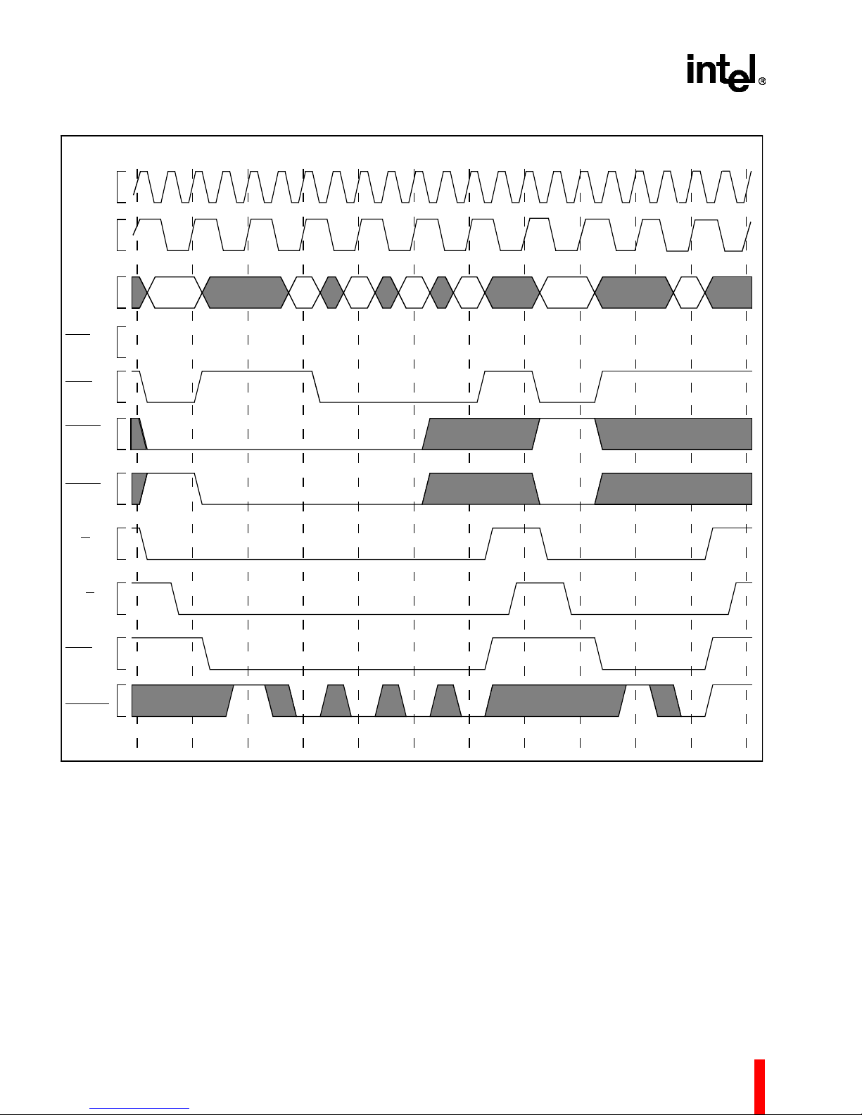
80960KB
CLK2
CLK
LAD31:0
ALE
ADS
BE3:2
BE1:0
W/R
T
a
T
w
T
d
T
d
T
T
d
d
T
r
T
a
T
w
T
d
T
r
DT/R
DEN
READY
Figure 30. Accesses Generated by Quad Word Read Bus Request, Misaligned Two Bytes from Quad
Word Boundary (1, 0, 0, 0 Wait States)
36
Page 43

80960KB
CLK2
CLK
INTR
LAD31:0
ALE
ADS
PREVIOUS
CYCLE
T
X
INTERRUPT
ACKNOWLEDGEMENT
CYCLE 1
T
T
a
ADDR
T
X
IDLE
(5 BUS STATES)
T
d
T
r
T
I
T
I
T
I
T
I
I
INTERRUPT
ACKNOWLEDGEMENT
CYCLE 2
T
a
ADDR
T
T
w
d
VECTOR
T
r
INTA
DT/R
DEN
LOCK
READY
NOTE:
INTR can go low no sooner than the input hold time following the beginning of interrupt acknowledgment cycle 1.
For a second interrupt to be acknowledged, INTR must be low for at least three cycles before it can be reasserted.
Figure 31. Interrupt Acknowledge Transaction
37
Page 44

80960KB
5.0 REVISION HISTORY
Revision -008
To address the fact that many of the package prefix variables have changed, all package
prefix variables in this document are now indicated with an "x".
No revision history was maintained in earlier revisions of this data sheet. All errata that has been
entified to date is incorporated into this revision. The sections significantly changed since the
id
Section
Table 4. 80960KB Pin
Description: L-Bus Signals (pg. 8)
2.3. Connection Recommendations (pg. 11)
Figure 9. Typical Current vs.
Frequency (Hot Temp) (pg. 13)
Figure 12. Test Load Circuit for
Three-State Output Pins (pg. 14)
Figure 13. Test Load Circuit for
Open-Drain Output Pins (pg. 14)
2.7. DC Characteristics (pg. 15) -005 ICC max specification reduced:
2.8. AC Specifications (pg. 16) -005 25 MHz operation extended to product in PQFP package. T
Functional Waveforms -005 Redrawn for clarity. CLK signal drawn with more likely phase
Various -005 Deleted all references to 10 MHz. Intel no longer offers a
Table 4. 80960KB Pin
Description: L-Bus Signals (pg. 8)
Figure 18, 80960KB PGA
Pinout—View from Bottom (Pins
Facing Up) (pg. 22)
previous revision are:
Last
Rev.
-005 LOCK
-005 Changed suggested open-drain termination networks to reflect
-005 Added figure for typical power supply current at hot
-005 All outputs now specified with standard 50 pF test loads to
-006 DEN pin description omitted from revision -005.
-006 Pin M2 was N.C., now shows as V
pin description rewritten for clarity.
more realistic operating conditions with reduction in DC power
consumption.
temperature to aid thermal analysis.
agree with actual test methodology.
WAS: IS: AT:
375 mA 315 mA 16 MHz
420 mA 360 mA 20 MHz
480 mA 420 mA 25 MHz
Figures 7, 8, 9, 23, 24, 25 and 26 have also been changed
accordingly.
min. improved at all frequencies from 0 ns to 2 ns and T
improved from 20 ns to 18 ns.
T8H max improvement:
WAS: IS: AT:
31ns 28ns 16 MHz
26ns 23ns 20 MHz
24ns 23ns 25 MHz
relationship to CLK2. Open-drain output signals drawn to show
correct inactive states.
10 MHz 80960KB device.
Pin M13 was VCC, now shows as N.C.
Description
CC
max.
8
8
38
 Loading...