

Page 1
查询80960JD供应商
A PRELIMINARY
■
Pin/Code Compatible with all 80960Jx
Processors
■ High-Performance Embedded Architecture
— One Instruction/Clock Execution
— Core Clock Rate is 2x the Bus Clock
— Load/Store Programming Model
— Sixteen 32-Bit Global Registers
— Sixteen 32-Bit Local Registers (8 sets)
— Nine Addressing Modes
— User/Supervisor Protection Model
■ Two-Way Set Associative Instruction Cache
— 80960JD - 4 Kbyte
— Programmable Cache Locking
Mechanism
■ Direct Mapped Data Cache
— 80960JD - 2 Kbyte
— Write Through Operation
■ On-Chip Stack Frame Cache
— Seven Register Sets Can Be Saved
— Automatic Allocation on Call/Return
— 0-7 Frames Reserved for High-Priority
Interrupts
■ On-Chip Data RAM
— 1 Kbyte Critical Variable Storage
— Single-Cycle Access
80960JD
EMBEDDED 32-BIT MICROPROCESSOR
■ High Bandwidth Burst Bus
— 32-Bit Multiplexed Address/Data
— Programmable Memory Configuration
— Selectable 8-, 16-, 32-Bit Bus Widths
— Supports Unaligned Accesses
— Big or Little Endian Byte Ordering
■ New Instructions
— Conditional Add, Subtract and Select
— Processor Management
■ High-Speed Interrupt Controller
— 31 Programmable Priorities
— Eight Maskable Pins plus NMI
— Up to 240 Vectors in Expanded Mode
■ Two On-Chip Timers
— Independent 32-Bit Counting
— Clock Prescaling by 1, 2, 4 or 8
— lnternal Interrupt Sources
■ Halt Mode for Low Power
■ IEEE 1149.1 (JTAG) Boundary Scan
Compatibility
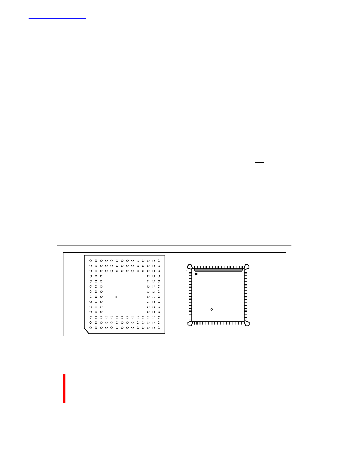
■ Packages
— 132-Lead Pin Grid Array (PGA)
— 132-Lead Plastic Quad Flat Pack (PQFP)
132
PIN 1
99
A
A80960JD
XXXXXXXXA2
M
© 19xx
i
33
Figure 1. 80960JD Microprocessor
Information in this document is provided solely to enable use of Intel products. Intel assumes no liability whatsoever, including infringement of any
patent or copyright, for sale and use of Intel products except as provided in Intel’s Terms and Conditions of Sale for such products. Information
contained herein supersedes previously published specifications on these devices from Intel.
© INTEL CORPORATION, 1995 September 1995 Order Number: 272596-002
i960
NG80960JD
XXXXXXXXA2
M
i
®
© 19xx
66
Page 2

A 80960JD
80960JD
EMBEDDED 32-BIT MICROPROCESSOR
1.0 PURPOSE ..................................................................................................................................................1
2.0 80960JD OVERVIEW .................................................................................................................................1
2.1 80960 Processor Core ........................................................................................................................2
2.2 Burst Bus ............................................................................................................................................2
2.3 Timer Unit ...........................................................................................................................................3
2.4 Priority Interrupt Controller .................................................................................................................3
2.5 Instruction Set Summary ....................................................................................................................3
2.6 Faults and Debugging .........................................................................................................................3
2.7 Low Power Operation .........................................................................................................................4
2.8 Test Features ......................................................................................................................................4
2.9 Memory-Mapped Control Registers ....................................................................................................4
2.10 Data Types and Memory Addressing Modes ....................................................................................4
3.0 PACKAGE INFORMATION ........................................................................................................................6
3.1 Pin Descriptions ..................................................................................................................................6
3.1.1 Functional Pin Definitions ........................................................................................................6
3.1.2 80960Jx 132-Lead PGA Pinout .............................................................................................13
3.1.3 80960Jx PQFP Pinout ...........................................................................................................17
3.2 Package Thermal Specifications ......................................................................................................20
3.3 Thermal Management Accessories ..................................................................................................22
4.0 ELECTRICAL SPECIFICATIONS ............................................................................................................23
4.1 Absolute Maximum Ratings ..............................................................................................................23
4.2 Operating Conditions ........................................................................................................................23
4.3 Connection Recommendations .........................................................................................................24
4.4 DC Specifications .............................................................................................................................24
4.5 AC Specifications ..............................................................................................................................26
4.5.1 AC Test Conditions and Derating Curves ...............................................................................33
4.5.2 AC Timing Waveforms ............................................................................................................34
5.0 BUS FUNCTIONAL WAVEFORMS .........................................................................................................42
6.0 DEVICE IDENTIFICATION .......................................................................................................................56
7.0 REVISION HISTORY ...............................................................................................................................56
PRELIMINARY
ii
Page 3

80960JD A
FIGURES
Figure 1. 80960JD Microprocessor ...........................................................................................................0
Figure 2. 80960JD Block Diagram ............................................................................................................2
Figure 3. 132-Lead Pin Grid Array Bottom View - Pins Facing Up ..........................................................13
Figure 4. 132-Lead Pin Grid Array Top View - Pins Facing Down ........................................................... 14
Figure 5. 132-Lead PQFP - Top View ..................................................................................................... 17
Figure 6. 50 MHz Maximum Allowable Ambient Temperature ................................................................ 21
Figure 7. 40 MHz Maximum Allowable Ambient Temperature ................................................................ 22
Figure 8. AC Test Load ............................................................................................................................33
Figure 9. Output Delay or Hold vs. Load Capacitance ............................................................................33
Figure 10. Rise and Fall Time Derating .....................................................................................................34
Figure 11. CLKIN Waveform ..................................................................................................................... 34
Figure 12. Output Delay Waveform for T
Figure 13. Output Float Waveform for T
Figure 14. Input Setup and Hold Waveform for T
Figure 15. Input Setup and Hold Waveform for T
Figure 16. Input Setup and Hold Waveform for T
Figure 17. Input Setup and Hold Waveform for T
Figure 18. Relative Timings Waveform for T
Figure 19. DT/R
and DEN Timings Waveform .......................................................................................... 38
Figure 20. TCK Waveform ......................................................................................................................... 39
Figure 21. Input Setup and Hold Waveforms for T
Figure 22. Output Delay and Output Float Waveform for T
Figure 23. Output Delay and Output Float Waveform for T
Figure 24. Input Setup and Hold Waveform for T
Figure 25. Non-Burst Read and Write Transactions Without Wait States, 32-Bit Bus ...............................42
Figure 26. Burst Read and Write Transactions Without Wait States, 32-Bit Bus ......................................43
Figure 27. Burst Write Transactions With 2,1,1,1 Wait States, 32-Bit Bus ................................................44
Figure 28. Burst Read and Write Transactions Without Wait States, 8-Bit Bus ........................................ 45
Figure 29. Burst Read and Write Transactions With 1, 0 Wait States
and Extra Tr State on Read, 16-Bit Bus ...................................................................................46
Figure 30. Bus Transactions Generated by Double Word Read Bus Request,
Misaligned One Byte From Quad Word Boundary, 32-Bit Bus, Little Endian ........................... 47
Figure 31. HOLD/HOLDA Waveform For Bus Arbitration .......................................................................... 48
Figure 32. Cold Reset Waveform ..............................................................................................................49
Figure 33. Warm Reset Waveform ............................................................................................................ 50
Figure 34. Entering the ONCE State .........................................................................................................51
Figure 35. Summary of Aligned and Unaligned Accesses (32-Bit Bus) ....................................................54
Figure 36. Summary of Aligned and Unaligned Accesses (32-Bit Bus) (Continued) ................................ 55
.............................................................................................35
OV1
................................................................................................35
OF
LXL
IS1
IS2
IS3
IS4
and T
BSIS1
BSIS2
and T
and T
and T
and T
................................................................... 36
IH1
................................................................... 36
IH2
...................................................................37
IH3
................................................................... 37
IH4
.........................................................................38
LXA
and T
BSOV1
BSOV2
and T
......................................................... 39
BSIH1
and T
and T
...........................................................41
BSIH2
.......................................... 40
BSOF1
.......................................... 40
BSOF2
iii
PRELIMINARY
Page 4

A 80960JD
TABLES
Table 1. 80960Jx Instruction Set ................................................................................................................5
Table 2. Pin Description Nomenclature ......................................................................................................6
Table 3. Pin Description — External Bus Signals ...................................................................................... 7
Table 4. Pin Description — Processor Control Signals, Test Signals and Power ..................................... 10
Table 5. Pin Description — Interrupt Unit Signals ....................................................................................12
Table 6. 132-Lead PGA Pinout — In Signal Order ................................................................................... 15
Table 7. 132-Lead PGA Pinout — In Pin Order .......................................................................................16
Table 8. 132-Lead PQFP Pinout — In Signal Order ................................................................................18
Table 9. 132-Lead PQFP Pinout — In Pin Order ..................................................................................... 19
Table 10. 132-Lead PGA Package Thermal Characteristics ...................................................................... 20
Table 11. 132-Lead PQFP Package Thermal Characteristics ................................................................... 21
Table 12. 80960JD Operating Conditions ..................................................................................................23
Table 13. 80960JD DC Characteristics ...................................................................................................... 24
Table 14. 80960JD I
Table 15. 80960JD AC Characteristics (50 MHz) ......................................................................................26
Table 16. Note Definitions for Table 15, 80960JD AC Characteristics (50 MHz) ......................................28
Table 17. 80960JD AC Characteristics (40 MHz) ......................................................................................28
Table 18. 80960JD AC Characteristics (33 MHz) ......................................................................................31
Table 19. Natural Boundaries for Load and Store Accesses .....................................................................52
Table 20. Summary of Byte Load and Store Accesses ..............................................................................52
Table 21. Summary of Short Word Load and Store Accesses ...................................................................52
Table 22. Summary of n-Word Load and Store Accesses (n = 1, 2, 3, 4) ..................................................53
Table 23. 80960JD Die and Stepping Reference ....................................................................................... 56
Table 24. Data Sheet Version -001 to -002 Revision History .....................................................................56
Characteristics ...................................................................................................... 25
CC
PRELIMINARY
iv
Page 5

A 80960JD
1.0 PURPOSE
This document contains advance information for the
80960JD microprocessor, including electrical
characteristics and package pinout information.
Detailed functional descriptions — other than
parametric performance — are published in the
®
Jx Microprocessor User’s Guide (272483).
i960
Throughout this data sheet, references to “80960Jx”
indicate features which apply to all of the following:
• 80960JA — 5V, 2 Kbyte instruction cache, 1 Kbyte
data cache
• 80960JF — 5V, 4 Kbyte instruction cache, 2 Kbyte
data cache
• 80960JD — 5V, 4 Kbyte instruction cache, 2 Kbyte
data cache and clock doubling
• 80L960JA — 3.3 V version of the 80960JA
• 80L960JF — 3.3 V version of the 80960JF
2.0 80960JD OVERVIEW
The 80960JD offers high performance to costsensitive 32-bit embedded applications. The
80960JD is object code compatible with the 80960
Core Architecture and is capable of sustained
execution at the rate of one instruction per clock.
This processor’s features include generous
instruction cache, data cache and data RAM. It also
boasts a fast interrupt mechanism, dual programmable timer units and new instructions.
The 80960JD’s clock doubler operates the processor
core at twice the bus clock rate to improve execution
performance without increasing the complexity of
board designs.
Memory subsystems for cost-sensitive embedded
applications often impose substantial wait state
penalties. The 80960JD integrates considerable
storage resources on-chip to decouple CPU
execution from the external bus.
The 80960JD rapidly allocates and deallocates local
register sets during context switches. The processor
needs to flush a register set to the stack only when it
saves more than seven sets to its local register
cache.
A 32-bit multiplexed burst bus provides a high-speed
interface to system memory and I/O. A full
complement of control signals simplifies the
connection of the 80960JD to external components.
The user programs physical and logical memory
attributes through memory-mapped control registers
(MMRs) — an extension not found on the i960 Kx,
Sx or Cx processors. Physical and logical configuration registers enable the processor to operate with
all combinations of bus width and data object
alignment. The processor supports a homogeneous
byte ordering model.
This processor integrates two important peripherals:
a timer unit and an interrupt controller. These and
other hardware resources are programmed through
memory-mapped control registers, an extension to
the familiar 80960 architecture.
The timer unit (TU) offers two independent 32-bit
timers for use as real-time system clocks and
general-purpose system timing. These operate in
either single-shot or auto-reload mode and can
generate interrupts.
The interrupt controller unit (ICU) provides a flexible
means for requesting interrupts. The ICU provides
full programmability of up to 240 interrupt sources
into 31 priority levels. The ICU takes advantage of a
cached priority table and optional routine caching to
minimize interrupt latency. Clock doubling reduces
interrupt latency by 40% compared to the
80960JA/JF. Local registers may be dedicated to
high-priority interrupts to further reduce latency.
Acting independently from the core, the ICU
compares the priorities of posted interrupts with the
current process priority, off-loading this task from the
core. The ICU also supports the integrated timer
interrupts.
The 80960JD features a Halt mode designed to
support applications where low power consumption
is critical. The halt instruction shuts down instruction
execution, resulting in a power savings of up to 90
percent.
The 80960JD’s testability features, including ONCE
(On-Circuit Emulation) mode and Boundary Scan
(JTAG), provide a powerful environment for design
debug and fault diagnosis.
The Solutions960® program features a wide variety
of development tools which support the i960
processor family. Many of these tools are developed
by partner companies; some are developed by Intel,
such as profile-driven optimizing compilers. For more
information on these products, contact your local
Intel representative.
PRELIMINARY
1
Page 6
80960JD A
SRC1
SRC2
DEST
SRC1
SRC2
DEST
SRC1
DEST
CLKIN
TAP
Local Register Cache
PLL, Clocks,
Power Mgmt
Boundary Scan
5
8-Set
128
Global / Local
Register File
SRC2 DESTSRC1
Controller
3 Independent 32-Bit SRC1, SRC2, and DEST Buses
4 KByte Instruction Cache
Two-Way Set Associative
Constants
and
Address
Unit
effective
address
Control
Multiply
Divide
Unit
Instruction Sequencer
Execution
Generation
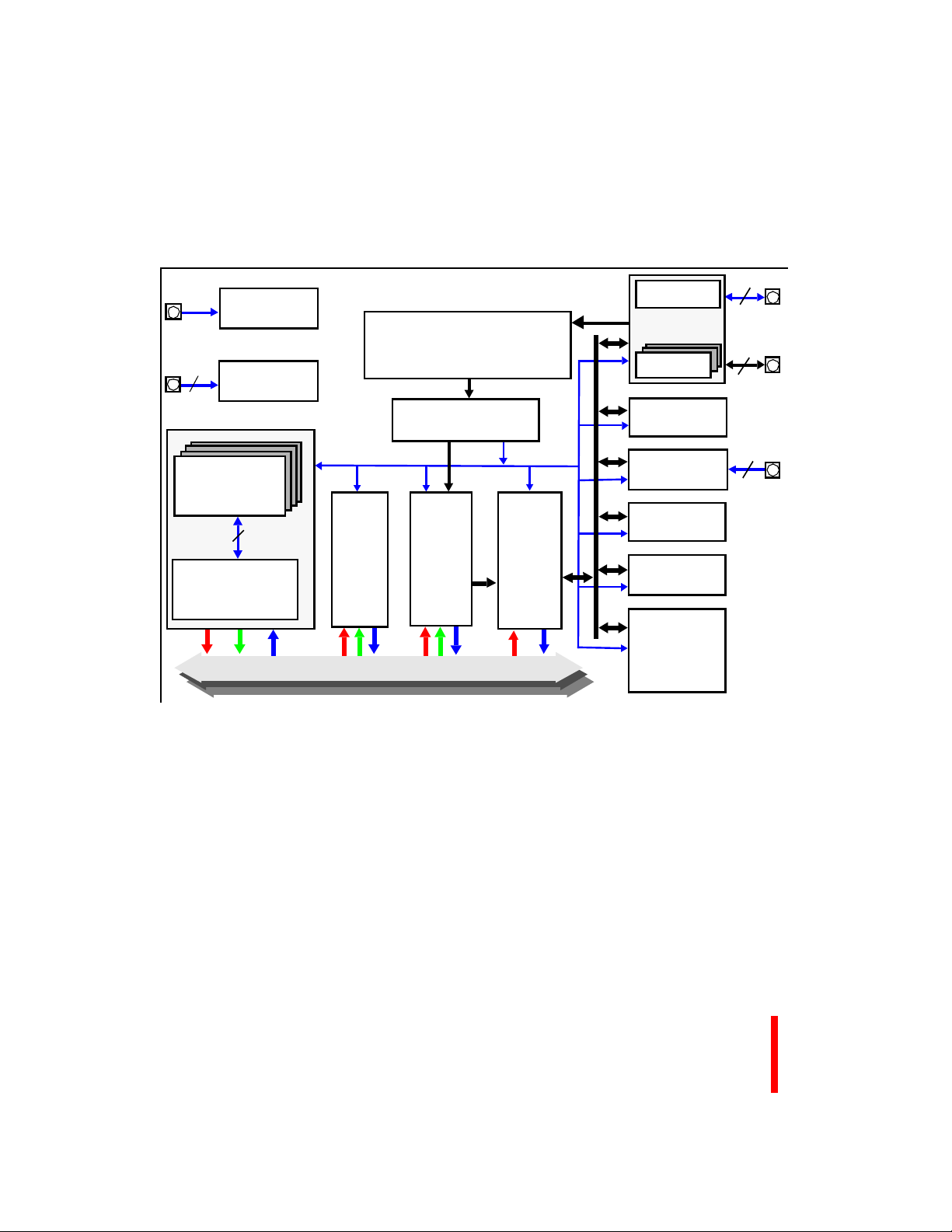
Figure 2. 80960JD Block Diagram
Memory
Interface
Unit
32-bit Address
32-bit Data
32-bit buses
address / data
Physical Region
Configuration
Bus
Control Unit
Bus Request
Queues
Two 32-Bit
Timers
Programmable
Interrupt Controller
Memory-Mapped
Register Interface
1 K byte
Data RAM
2 Kbyte Direct
Mapped Data
Cache
Control
21
Address/
Data Bus
32
Interrupt
Port
9
2.1 80960 Processor Core
The 80960Jx family is a scalar implementation of the
80960 Core Architecture. Intel designed this
processor core as a very high performance device
that is also cost-effective. Factors that contribute to
the core’s performance include:
• Core operates at twice the bus speed (80960JD
only)
• Single-clock execution of most instructions
• Independent Multiply/Divide Unit
• Efficient instruction pipeline minimizes pipeline
break latency
• Register and resource scoreboarding allow
overlapped instruction execution
2
• 128-bit register bus speeds local register caching
• 4 Kbyte two-way set associative, integrated
instruction cache
• 2 Kbyte direct-mapped, integrated data cache
• 1 Kbyte integrated data RAM delivers zero wait
state program data
2.2 Burst Bus
A 32-bit high-performance bus controller interfaces
the 80960JD to external memory and peripherals.
The BCU fetches instructions and transfers data at
the rate of up to four 32-bit words per six clock
cycles. The external address/data bus is multiplexed.
PRELIMINARY
Page 7

A 80960JD
Users may configure the 80960JD’s bus controller to
match an application’s fundamental memory organization. Physical bus width is register-programmed for
up to eight regions. Byte ordering and data caching
are programmed through a group of logical memory
templates and a defaults register.
The BCU’s features include:
• Multiplexed external bus to minimize pin count
• 32-, 16- and 8-bit bus widths to simplify I/O
interfaces
• External ready control for address-to-data, data-todata and data-to-next-address wait state types
• Support for big or little endian byte ordering to
facilitate the porting of existing program code
• Unaligned bus accesses performed transparently
• Three-deep load/store queue to decouple the bus
from the core
Upon reset, the 80960JD conducts an internal self
test. Then, before executing its first instruction, it
performs an external bus confidence test by
performing a checksum on the first words of the
initialization boot record (IBR).
The user may examine the contents of the caches at
any time by executing special cache control instructions.
2.3 Timer Unit
The timer unit (TU) contains two independent 32-bit
timers which are capable of counting at several clock
rates and generating interrupts. Each is programmed
by use of the TU registers. These memory-mapped
registers are addressable on 32-bit boundaries. The
timers have a single-shot mode and auto-reload
capabilities for continuous operation. Each timer has
an independent interrupt request to the 80960JD’s
interrupt controller. The TU can generate a fault
when unauthorized writes from user mode are
detected. Clock prescaling is supported.
2.4 Priority Interrupt Controller
A programmable interrupt controller manages up to
240 external sources through an 8-bit external
interrupt port. Alternatively, the interrupt inputs may
be configured for individual edge- or level-triggered
inputs. The interrupt unit (IU) also accepts interrupts
from the two on-chip timer channels and a single
Non-Maskable Interrupt (NMI
serviced according to their priority levels relative to
the current process priority.
Low interrupt latency is critical to many embedded
applications. As part of its highly flexible interrupt
mechanism, the 80960JD exploits several
techniques to minimize latency:
• Interrupt vectors and interrupt handler routines can
be reserved on-chip
• Register frames for high-priority interrupt handlers
can be cached on-chip
• The interrupt stack can be placed in cacheable
memory space
• Interrupt microcode executes at twice the bus
frequency
) pin. Interrupts are
2.5 Instruction Set Summary
The 80960Jx adds several new instructions to the
i960 core architecture. The new instructions are:
• Conditional Move
• Conditional Add
• Conditional Subtract
• Byte Swap
• Halt
• Cache Control
• Interrupt Control
Table 1 identifies the instructions that the 80960Jx
supports. Refer to i960
Guide (272483) for a detailed description of each
instruction.
®
Jx Microprocessor User’s
2.6 Faults and Debugging
The 80960Jx employs a comprehensive fault model.
The processor responds to faults by making implicit
calls to a fault handling routine. Specific information
collected for each fault allows the fault handler to
diagnose exceptions and recover appropriately.
The processor also has built-in debug capabilities. In
software, the 80960Jx may be configured to detect
as many as seven different trace event types. Alter-
PRELIMINARY
3
Page 8

80960JD A
natively, mark and fmark instructions can generate
trace events explicitly in the instruction stream.
Hardware breakpoint registers are also available to
trap on execution and data addresses.
2.7 Low Power Operation
Intel fabricates the 80960Jx using an advanced submicron manufacturing process. The processor’s submicron topology provides the circuit density for
optimal cache size and high operating speeds while
dissipating modest power. The processor also uses
dynamic power management to turn off clocks to
unused circuits.
Users may program the 80960Jx to enter Halt mode
for maximum power savings. In Halt mode, the
processor core stops completely while the integrated
peripherals continue to function, reducing overall
power requirements up to 90 percent. Processor
execution resumes from internally or externally
generated interrupts.
2.8 Test Features
The 80960Jx incorporates numerous features which
enhance the user’s ability to test both the processor
and the system to which it is attached. These
features include ONCE (On-Circuit Emulation) mode
and Boundary Scan (JTAG).
The 80960Jx provides testability features compatible
with IEEE Standard Test Access Port and Boundary
Scan Architecture (IEEE Std. 1149.1).
One of the boundary scan instructions, HIGHZ,
forces the processor to float all its output pins
(ONCE mode). ONCE mode can also be initiated at
reset without using the boundary scan mechanism.
ONCE mode is useful for board-level testing. This
feature allows a mounted 80960JD to electrically
“remove” itself from a circuit board. This allows for
system-level testing where a remote tester — such
as an in-circuit emulator — can exercise the
processor system.
The provided test logic does not interfere with
component or circuit board behavior and ensures
that components function correctly, connections
between various components are correct, and
various components interact correctly on the printed
circuit board.
The JTAG Boundary Scan feature is an attractive
alternative to conventional “bed-of-nails” testing. It
can examine connections which might otherwise be
inaccessible to a test system.
2.9 Memory-Mapped Control
Registers
The 80960JD, though compliant with i960 series
processor core, has the added advantage of
memory-mapped, internal control registers not found
on the i960 Kx, Sx or Cx processors. These give
software the interface to easily read and modify
internal control registers.
Each of these registers is accessed as a memorymapped, 32-bit register. Access is accomplished
through regular memory-format instructions. The
processor ensures that these accesses do not
generate external bus cycles.
2.10 Data Types and Memory
Addressing Modes
As with all i960 family processors, the 80960Jx
instruction set supports several data types and
formats:
• Bit
• Bit fields
• Integer (8-, 16-, 32-, 64-bit)
• Ordinal (8-, 16-, 32-, 64-bit unsigned integers)
• Triple word (96 bits)
• Quad word (128 bits)
The 80960Jx provides a full set of addressing modes
for C and assembly programming:
• Two Absolute modes
• Five Register Indirect modes
• Index with displacement
• IP with displacement
4
PRELIMINARY
Page 9

A 80960JD
Table 1. 80960Jx Instruction Set
Data Movement Arithmetic Logical Bit, Bit Field and Byte
Load
Store
Move
*Conditional Select
Load Address
Comparison Branch Call/Return Fault
Compare
Conditional Compare
Compare and
Increment
Compare and
Decrement
Test Condition Code
Check Bit
Debug
Modify Trace Controls
Mark
Force Mark
NOTE: Asterisk (*) denotes new 80960Jx instructions unavailable on 80960CA/CF, 80960KA/KB and 80960SA/SB implementations.
Add
Subtract
Multiply
Divide
Remainder
Modulo
Shift
Extended Shift
Extended Multiply
Extended Divide
Add with Carry
Subtract with Carry
*Conditional Add
*Conditional Subtract
Rotate
Unconditional Branch
Conditional Branch
Compare and Branch
Processor
Management
Flush Local Registers
Modify Arithmetic
Controls
Modify Process
Controls
*Halt
System Control
*Cache Control
*Interrupt Control
And
Not And
And Not
Or
Exclusive Or
Not Or
Or Not
Nor
Exclusive Nor
Not
Nand
Call
Call Extended
Call System
Return
Branch and Link
Atomic
Atomic Add
Atomic Modify
Set Bit
Clear Bit
Not Bit
Alter Bit
Scan For Bit
Span Over Bit
Extract
Modify
Scan Byte for Equal
*Byte Swap
Conditional Fault
Synchronize Faults
PRELIMINARY
5
Page 10

80960JD A
3.0 PACKAGE INFORMATION
The 80960JD is offered in several speed and
package types. The 132-pin Pin Grid Array (PGA)
device will be specified for operation at
= 5.0 V ± 5% over a case temperature range of
V
cc
0° to 85°C:
• A80960JD-50 (50 MHz core, 25 MHz bus)
The 132-pin Pin Grid Array (PGA) device will be
specified for operation at V
case temperature range of 0° to 100°C:
= 5.0 V ± 5% over a
cc
• A80960JD-40 (40 MHz core, 20 MHz bus)
• A80960JD-33 (33.33 MHz core, 16.67 MHz bus)
The 132-pin Plastic Quad Flatpack (PQFP) devices
will be specified for operation at V
over a case temperature range of 0° to 100°C:
= 5.0 V ± 5%
cc
• NG80960JD-40 (40 MHz core, 20 MHz bus)
• NG80960JD-33 (33.33 MHz core, 16.67 MHz bus)
For complete package specifications and infor-
mation, refer to Intel’s Packaging Handbook
(240800).
3.1 Pin Descriptions
This section describes the pins for the 80960JD in
the 132-pin ceramic Pin Grid Array (PGA) package
and 132-lead Plastic Quad Flatpack Package
(PQFP).
Section 3.1.1, Functional Pin Definitions
describes pin function; Section 3.1.2, 80960Jx 132Lead PGA Pinout and Section 3.1.3, 80960Jx
PQFP Pinout define the signal and pin locations for
the supported package types.
3.1.1 Functional Pin Definitions
Table 2 presents the legend for interpreting the pin
descriptions which follow. Pins associated with the
bus interface are described in Table 3. Pins
associated with basic control and test functions are
described in Table 4. Pins associated with the
Interrupt Unit are described in Table 5.
Table 2. Pin Description Nomenclature
Symbol Description
I Input pin only.
O Output pin only.
I/O Pin can be either an input or output.
– Pin must be connected as described.
S Synchronous. Inputs must meet setup
and hold times relative to CLKIN for
proper operation.
S(E) Edge sensitive input
S(L) Level sensitive input
A (...) Asynchronous. Inputs may be
asynchronous relative to CLKIN.
A(E) Edge sensitive input
A(L) Level sensitive input
R (...) While the processor’s RESET
pin is
asserted, the pin:
R(1) is driven to V
R(0) is driven to V
R(Q) is a valid output
CC
SS
R(X) is driven to unknown state
R(H) is pulled up to V
CC
H (...) While the processor is in the hold state,
the pin:
H(1) is driven to V
H(0) is driven to V
H(Q) Maintains previous state or
CC
SS
continues to be a valid output
H(Z) Floats
P (...) While the processor is halted, the pin:
P(1) is driven to V
P(0) is driven to V
P(Q) Maintains previous state or
CC
SS
continues to be a valid output
6
PRELIMINARY
Page 11

A 80960JD
Table 3. Pin Description — External Bus Signals (Sheet 1 of 4)
NAME TYPE DESCRIPTION
AD31:0 I/O
S(L)
R(X)
H(Z)
P(Q)
ADDRESS / DATA BUS carries 32-bit physical addresses and 8-, 16- or 32-bit data
T
to and from memory. During an address (
address (bits 0-1 indicate SIZE; see below). During a data (T
) cycle, bits 31:2 contain a physical word
a
data is present on one or more contiguous bytes, comprising AD31:24, AD23:16,
AD15:8 and AD7:0. During write operations, unused pins are driven to determinate
values.
SIZE, which comprises bits 0-1 of the AD lines during a
number of data transfers during the bus transaction.
AD1 AD0 Bus Transfers
0 0 1 Transfer
0 1 2 Transfers
1 0 3 Transfers
1 1 4 Transfers
When the processor enters Halt mode, if the previous bus operation was a:
• write — AD31:2 are driven with the last data value on the AD bus.
• read — AD31:4 are driven with the last address value on the AD bus; AD3:2 are
driven with the value of A3:2 from the last data cycle.
Typically, AD1:0 reflect the SIZE information of the last bus transaction (either
instruction fetch or load/store) that was executed before entering Halt mode.
ALE O
R(0)
H(Z)
ADDRESS LATCH ENABLE indicates the transfer of a physical address. ALE is
T
asserted during a
active HIGH and floats to a high impedance state during a hold cycle (T
cycle and deasserted before the beginning of the Td state. It is
a
P(0)
ADDRESS LATCH ENABLE indicates the transfer of a physical address. ALE
ALE
O
R(1)
H(Z)
inverted version of ALE. This signal gives the 80960JD a high degree of compatibility
with existing 80960Kx systems.
P(1)
ADDRESS STROBE indicates a valid address and the start of a new bus access.
ADS
O
R(1)
H(Z)
The processor asserts ADS
samples ADS
at the end of the cycle.
for the entire Ta cycle. External bus control logic typically
P(1)
A3:2 O
R(X)
H(Z)
P(Q)
ADDRESS3:2 comprise a partial demultiplexed address bus.
32-bit memory accesses: the processor asserts address bits A3:2 during
partial word address increments with each assertion of RDYRCV
16-bit memory accesses: the processor asserts address bits A3:1 during
driven on the
of RDYRCV
BE1 pin. The partial short word address increments with each assertion
during a burst.
8-bit memory accesses: the processor asserts address bits A3:0 during
driven on BE1:0
RDYRCV
. The partial byte address increments with each assertion of
during a burst.
) cycle, read or write
d
T
cycle, specifies the
a
h
during a burst.
T
).
is the
T
. The
a
T
with A1
a
, with A1:0
a
PRELIMINARY
7
Page 12
80960JD A
Table 3. Pin Description — External Bus Signals (Sheet 2 of 4)
NAME TYPE DESCRIPTION
BE3:0 O
R(1)
H(Z)
P(1)
WIDTH/
HLTD1:0
R(0)
H(Z)
P(1)
D/C
R(X)
H(Z)
P(Q)
W/R
R(0)
H(Z)
P(Q)
BYTE ENABLES select which of up to four data bytes on the bus participate in the
current bus access. Byte enable encoding is dependent on the bus width of the
memory region accessed:
32-bit bus:
enables data on AD31:24
BE3
enables data on AD23:16
BE2
enables data on AD15:8
BE1
enables data on AD7:0
BE0
16-bit bus:
becomes Byte High Enable (enables data on AD15:8)
BE3
is not used (state is high)
BE2
becomes Address Bit 1 (A1)
BE1
becomes Byte Low Enable (enables data on AD7:0)
BE0
8-bit bus:
is not used (state is high)
BE3
is not used (state is high)
BE2
becomes Address Bit 1 (A1)
BE1
becomes Address Bit 0 (A0)
BE0
The processor asserts byte enables, byte high enable and byte low enable during
Since unaligned bus requests are split into separate bus transactions, these signals
do not toggle during a burst. They remain active through the last T
cycle.
d
For accesses to 8- and 16-bit memory, the processor asserts the address bits in
conjunction with A3:2 described above.
WIDTH/HALTED signals denote the physical memory attributes for a bus transaction:
O
WIDTH/HLTD1 WIDTH/HLTD0
0 0 8 Bits Wide
0 1 16 Bits Wide
1 0 32 Bits Wide
1 1 Processor Halted
The processor floats the WIDTH/HLTD pins whenever it relinquishes the bus in
response to a HOLD request, regardless of prior operating state.
DATA/CODE indicates that a bus access is a data access (1) or an instruction access
O
has the same timing as W/R.
(0). D/C
0 = instruction access
1 = data access
WRITE/READ specifies, during a
O
(0). It is latched on-chip and remains valid during T
T
cycle, whether the operation is a write (1) or read
a
cycles.
d
0 = read
1 = write
T
.
a
8
PRELIMINARY
Page 13
A 80960JD
Table 3. Pin Description — External Bus Signals (Sheet 3 of 4)
NAME TYPE DESCRIPTION
DT/R O
DEN
BLAST
RDYRCV
/
LOCK
ONCE
R(0)
H(Z)
P(Q)
R(1)
H(Z)
P(1)
R(1)
H(Z)
P(1)
S(L)
S(L)
R(H)
H(Z)
P(1)
DATA TRANSMIT / RECEIVE indicates the direction of data transfer to and from the
address/data bus. It is low during T
/Td cycles for a write. DT/R never changes state when DEN is asserted.
and T
w
0 = receive
1 = transmit
DATA ENABLE indicates data transfer cycles during a bus access. DEN
O
at the start of the first data cycle in a bus access and deasserted at the end of the last
data cycle. DEN
to the data bus.
0 = data cycle
1 = not data cycle
BURST LAST indicates the last transfer in a bus access. BLAST
O
last data transfer of burst and non-burst accesses. BLAST
wait states are inserted via the RDYRCV
data transfer in a bus cycle.
0 = last data transfer
1 = not last data transfer
I
READY/RECOVER indicates that data on AD lines can be sampled or removed. If
RDYRCV
by inserting a wait state (T
0 = sample data
1 = don’t sample data
The RDYRCV
continues to insert additional recovery states until it samples the pin HIGH. This
function gives slow external devices more time to float their buffers before the
processor begins to drive address again.
0 = insert wait states
1 = recovery complete
BUS LOCK indicates that an atomic read-modify-write operation is in progress. The
I/O
output is asserted in the first clock of an atomic operation and deasserted in
LOCK
the last data transfer of the sequence. The processor does not grant HOLDA while it
is asserting LOCK
semaphore operations.
0 = Atomic read-modify-write in progress
1 = Atomic read-modify-write not in progress
ONCE MODE: The processor samples the ONCE
LOW at the end of reset, the processor enters ONCE mode. In ONCE mode, the
processor stops all clocks and floats all output pins. The pin has a weak internal
pullup which is active during reset to ensure normal operation when the pin is left
unconnected.
0 = ONCE mode enabled
1 = ONCE mode not enabled
is used with DT/R to provide control for data transceivers connected
is not asserted during a Td cycle, the Td cycle is extended to the next cycle
w
pin has another function during the recovery (Tr) state. The processor
. This prevents external agents from accessing memory involved in
and Tw/Td cycles for a read; it is high during Ta
a
is asserted in the
pin. BLAST becomes inactive after the final
).
remains active as long as
input during reset. If it is asserted
is asserted
PRELIMINARY
9
Page 14

80960JD A
Table 3. Pin Description — External Bus Signals (Sheet 4 of 4)
NAME TYPE DESCRIPTION
HOLD I
S(L)
HOLDA O
R(Q)
H(1)
P(Q)
BSTAT O
R(0)
H(Q)
P(0)
Table 4. Pin Description — Processor Control Signals, Test Signals and Power (Sheet 1 of 2)
NAME TYPE DESCRIPTION
CLKIN I CLOCK INPUT provides the processor’s fundamental time base; both the processor
RESET
A(L)
STEST I
S(L)
HOLD: A request from an external bus master to acquire the bus. When the
processor receives HOLD and grants bus control to another master, it asserts
HOLDA, floats the address/data and control lines and enters the T
HOLD is deasserted, the processor deasserts HOLDA and enters either the T
state. When
h
state, resuming control of the address/data and control lines.
0 = no hold request
1 = hold request
HOLD ACKNOWLEDGE indicates to an external bus master that the processor has
relinquished control of the bus. The processor can grant HOLD requests and enter
state during reset and while halted as well as during regular operation.
the T
h
0 = hold not acknowledged
1 = hold acknowledged
BUS STATUS indicates that the processor may soon stall unless it has sufficient
access to the bus; see i960
®
Jx Microprocessor User’s Guide (272483). Arbitration
logic can examine this signal to determine when an external bus master should
acquire/relinquish the bus.
0 = no potential stall
1 = potential stall
core and the external bus run at the CLKIN rate. All input and output timings are
specified relative to a rising CLKIN edge.
I
RESET initializes the processor and clears its internal logic. During reset, the
processor places the address/data bus and control output pins in their idle (inactive)
states.
During reset, the input pins are ignored with the exception of LOCK
/ONCE, STEST
and HOLD.
The RESET
ization during power up, RESET
cycles with V
a minimum of 15 cycles.
pin has an internal synchronizer. To ensure predictable processor initial-
must be asserted a minimum of 10,000 CLKIN
and CLKIN stable. On a warm reset, RESET should be asserted for
CC
SELF TEST enables or disables the processor’s internal self-test feature at initialization. STEST is examined at the end of reset. When STEST is asserted, the
processor performs its internal self-test and the external bus confidence test. When
STEST is deasserted, the processor performs only the external bus confidence test.
0 = self test disabled
1 = self test enabled
or Ta
i
10
PRELIMINARY
Page 15

A 80960JD
Table 4. Pin Description — Processor Control Signals, Test Signals and Power (Sheet 2 of 2)
NAME TYPE DESCRIPTION
FAIL O
TCK I TEST CLOCK is a CPU input which provides the clocking function for IEEE 1149.1
TDI I
TDO O
TRST
TMS I
V
CC
V
CCPLL
V
SS
NC – NO CONNECT pins. Do not make any system connections to these pins.
R(0)
H(Q)
P(1)
S(L)
R(Q)
HQ)
P(Q)
A(L)
S(L)
FAIL indicates a failure of the processor’s built-in self-test performed during initialization. FAIL
indicate the status of individual tests:
• When self-test passes, the processor deasserts FAIL
user code.
• When self-test fails, the processor asserts FAIL
0 = self test failed
1 = self test passed
Boundary Scan Testing (JTAG). State information and data are clocked into the
processor on the rising edge; data is clocked out of the processor on the falling edge.
TEST DATA INPUT is the serial input pin for JTAG. TDI is sampled on the rising edge
of TCK, during the SHIFT-IR and SHIFT-DR states of the Test Access Port.
TEST DATA OUTPUT is the serial output pin for JTAG. TDO is driven on the falling
edge of TCK during the SHIFT-IR and SHIFT-DR states of the Test Access Port. At
other times, TDO floats. TDO does not float during ONCE mode.
I
TEST RESET asynchronously resets the Test Access Port (TAP) controller function
of IEEE 1149.1 Boundary Scan testing (JTAG). When using the Boundary Scan
feature, connect a pulldown resistor between this pin and V
pin must be connected to V
Connection Recommendations (pg. 24).
TEST MODE SELECT is sampled at the rising edge of TCK to select the operation
of the test logic for IEEE 1149.1 Boundary Scan testing.
– POWER pins intended for external connection to a VCC board plane.
– PLL POWER is a separate VCC supply pin for the phase lock loop clock generator. It
is intended for external connection to the V
add a simple bypass filter circuit to reduce noise-induced clock jitter and its effects on
timing relationships.
– GROUND pins intended for external connection to a VSS board plane.
is asserted immediately upon reset and toggles during self-test to
and begins operation from
and then stops executing.
. If TAP is not used, this
; however, no resistor is required. See Section 4.3,
SS
board plane. In noisy environments,
CC
SS
PRELIMINARY
11
Page 16

80960JD A
Table 5. Pin Description — Interrupt Unit Signals
NAME TYPE DESCRIPTION
I
XINT7:0
A(E/L)
NMI
A(E)
EXTERNAL INTERRUPT pins are used to request interrupt service. The XINT7:0
pins can be configured in three modes:
Dedicated Mode: Each pin is assigned a dedicated interrupt level. Dedicated inputs
can be programmed to be level (low) or edge (falling) sensitive.
Expanded Mode: All eight pins act as a vectored interrupt source. The interrupt pins
are level sensitive in this mode.
Mixed Mode: The XINT7:5
pins act as dedicated sources and the XINT4:0 pins
act as the five most significant bits of a vectored source. The least
significant bits of the vectored source are set to 010
Unused external interrupt pins should be connected to V
I
NON-MASKABLE INTERRUPT causes a non-maskable interrupt event to occur.
is the highest priority interrupt source and is falling edge-triggered. If NMI is
NMI
unused, it should be connected to V
CC
.
CC
.
internally.
2
12
PRELIMINARY
Page 17
A 80960JD
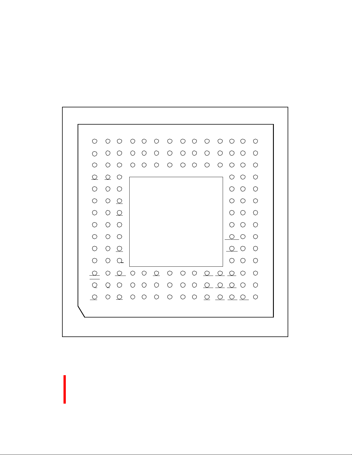
3.1.2 80960Jx 132-Lead PGA Pinout
1413121110987654321
P
AD18AD19AD22AD25
CC
CC
CC
CC
CC
CC
CC
V
V
V
V
V
V
AD6AD11AD13V
N
AD20AD24AD26AD27
SS
SS
SS
SS
SS
SS
SS
V
V
V
V
V
V
AD3AD7AD10V
M
AD1
V
V
V
V
V
V
TCKXINT3
AD0AD4AD8AD9AD12AD14AD15AD16AD17AD21AD23
V
CC
V
CC
SS
V
CC
SS
CLKINV
SS
V
CC
SS
V
CC
SS
V
CC
SS
V
CC
SS
NCSTESTTRSTHOLDNCFAIL NCBLAST
NC
TMSXINT2
AD29AD30 NC
L
K
BE2
V
BE3
AD28
AD31V
SS
CC
J
SS
SS
V
SS
V
SS
V
SS
SS
HOLDA
WIDTH/ADS
HLTD1
BE1V
BE0V
ALEV
BSTAT
DEN
DT/RV
A3 XINT1
A2
V
V
HLTD0
NCTDOWIDTH/D/CW/R XINT4
NCNCALE
SS
SS
V
V
CC
CC
V
SS
V
CC
XINT6V
SS
CC
V
CC
H
G
F
E
D
C
B
V
CC
CC
V
CC
V
CC
V
CC
LOCK/
ONCE
A
XINT0
AD5
AD2
NC
V
CCPLL
NC
RDYRCV
RESET
TDI
XINT5XINT7NMIV
P
N
M
L
K
J
H
G
F
E
D
C
B
A
Figure 3. 132-Lead Pin Grid Array Bottom View - Pins Facing Up
PRELIMINARY
1413121110987654321
13
Page 18
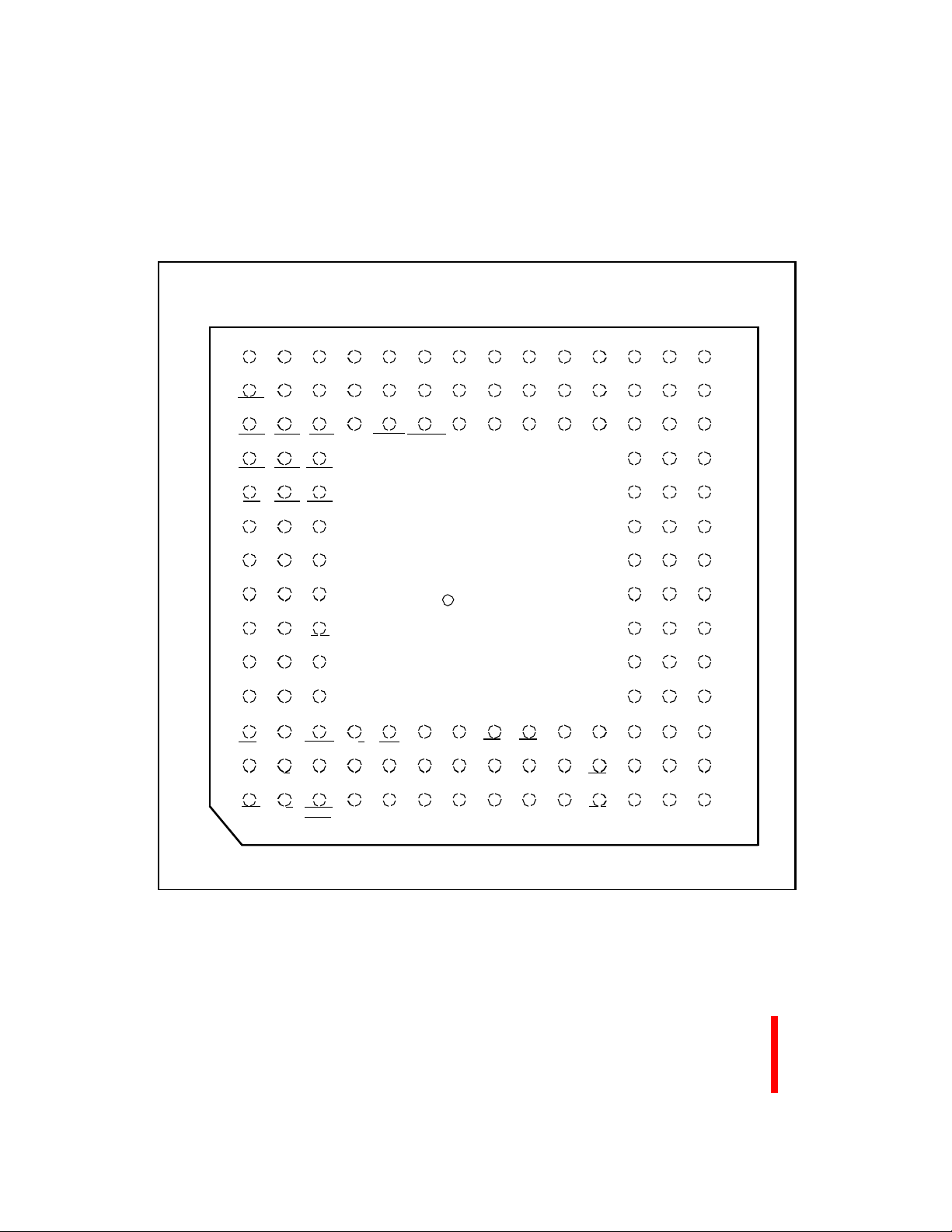
80960JD A
PNMLKJHGFEDCBA
14
TMS NC NC VCCVCCVCCVCCCLKIN VCCVCCVCCAD0 AD3 AD6
13
12
11
10
9
8
7
6
5
4
3
2
1
XINT2
TCK STEST VSSVSSVSSVSSVSSVSSVSSAD1 AD4 AD7 AD11
XINT5
XINT3 TRST
XINT4
NC
WIDTH/
HLTD0
D/C
W/R
XINT0
XINT1
BLAST
HOLDA
LOCK/
ONCE
XINT7
NMI XINT6
VCCVSSHOLD
V
CCVSS
V
CCVSS
V
CCVSS
NC A2
NC TDO
ALE
WIDTH/
HLTD1
ADS
TDI
RDYRCV NC V
RESET
CCPLL
A80960JD
NC
M
NC
FAIL
A3
DT/R
i
XXXXXXXX A2
DEN
V
V
SS
SSVSSVSSVSSVSSVSS
VCCVCCVCCVCCVCCVCCVCCBE2 AD30
© 19xx
BSTAT ALE BE1BE0
NC
AD2 AD5
AD31
AD28
BE3 AD29
AD10 AD13AD8
AD9 V
SSVCC
AD12 VSSV
AD14 VSSV
AD15 VSSV
AD16
AD17 V
AD21 VSSV
AD23 AD20 AD18
NC
AD24
AD27 AD25
V
SS
V
SS
AD26
V
AD19
AD22
CC
CC
CC
CC
CC
CC
14
13
12
11
10
9
8
7
6
5
4
3
2
1
14
PNMLKJHGFEDCBA
Figure 4. 132-Lead Pin Grid Array Top View - Pins Facing Down
PRELIMINARY
Page 19

A 80960JD
Table 6. 132-Lead PGA Pinout — In Signal Order
Signal Pin Signal Pin Signal Pin Signal Pin
A2 C5 AD31 K3 TDI D12 V
A3 C4 ADS
A1 TDO B4 V
AD0 M14 ALE G3 TMS A14 V
AD1 L13 ALE
AD2 K12 BE0
AD3 N14 BE1
AD4 M13 BE2
AD5 L12 BE3
AD6 P14 BLAST
AD7 N13 BSTAT F3 V
AD8 M12 CLKIN H14 V
AD9 M11 D/C
AD10 N12 DEN
AD11 P13 DT/R
AD12 M10 FAIL
AD13 P12 HOLD C9 V
AD14 M9 HOLDA C2 V
AD15 M8 LOCK
/ONCE C1 V
AD16 M7 NC A4 V
AD17 M6 NC A5 V
AD18 P4 NC B5 V
AD19 P3 NC B14 V
AD20 N4 NC C7 V
AD21 M5 NC C8 V
AD22 P2 NC C14 V
AD23 M4 NC G12 V
AD24 N3 NC J12 V
AD25 P1 NC M3 V
AD26 N2 NMI
AD27 N1 RDYRCV
AD28 L3 RESET
AD29 M2 STEST C13 V
AD30 M1 TCK B13 V
A3 TRST C12 V
H3 V
J3 V
L1 V
L2 V
C3 V
B2 V
E3 V
D3 V
C6 V
A10 V
F12 V
E12 V
CC
CC
CC
CC
CC
CC
CC
CC
CC
CC
CC
CC
CC
CC
CC
CC
CC
CC
CC
CC
CC
CC
CC
CC
CC
CCPLL
SS
SS
SS
A6 V
A7 V
A8 V
A9 V
D1 V
D14 V
E1 V
E14 V
F1 V
F14 V
G1 V
G14 V
H1 V
J1 V
J14 V
K1 V
K14 V
L14 V
P5 W/R B1
P6 WIDTH/HLTD0 B3
P7 WIDTH/HLTD1 A2
P8 XINT0 C11
P9 XINT1 C10
P10 XINT2 A13
P11 XINT3 B12
H12 XINT4 B11
B6 XINT5 A12
B7 XINT6 B10
B8 XINT7 A11
NOTE: Do not connect any external logic to pins marked NC (no connect pins).
SS
SS
SS
SS
SS
SS
SS
SS
SS
SS
SS
SS
SS
SS
SS
SS
SS
SS
SS
SS
SS
SS
B9
D2
D13
E2
E13
F2
F13
G2
G13
H2
H13
J2
J13
K2
K13
N5
N6
N7
N8
N9
N10
N11
PRELIMINARY
15
Page 20

80960JD A
Table 7. 132-Lead PGA Pinout — In Pin Order
Pin Signal Pin Signal Pin Signal Pin Signal
A1 ADS
A2 WIDTH/HLTD1 C7 NC H2 V
A3 ALE
A4 NC C9 HOLD H12 V
A5 NC C10 XINT1
A6 V
A7 V
A8 V
A9 V
CC
CC
CC
CC
A10 NMI
A11 XINT7 D2 V
A12 XINT5 D3 DT/R J14 V
A13 XINT2 D12 TDI K1 V
A14 TMS D13 V
B1 W/R D14 V
B2 D/C E1 V
B3 WIDTH/HLTD0 E2 V
B4 TDO E3 DEN
B5 NC E12 RESET
B6 V
B7 V
B8 V
B9 V
SS
SS
SS
SS
B10 XINT6
C6 FAIL H1 V
CC
SS
C8 NC H3 BE0 M12 AD8
CCPLL
H13 V
SS
C11 XINT0 H14 CLKIN N1 AD27
C12 TRST J1 V
C13 STEST J2 V
CC
SS
C14 NC J3 BE1 N4 AD20
D1 V
CC
SS
SS
CC
CC
SS
J12 NC N5 V
J13 V
K2 V
SS
CC
CC
SS
K3 AD31 N10 V
K12 AD2 N11 V
K13 V
K14 V
SS
CC
L1 BE2 N14 AD3
E13 V
E14 V
F1 V
F2 V
SS
CC
CC
SS
F3 BSTAT L14 V
L2 BE3 P1 AD25
L3 AD28 P2 AD22
L12 AD5 P3 AD19
L13 AD1 P4 AD18
CC
B11 XINT4 F12 RDYRCV M1 AD30 P6 V
B12 XINT3 F13 V
B13 TCK F14 V
B14 NC G1 V
C1 LOCK/ONCE G2 V
SS
CC
CC
SS
M2 AD29 P7 V
M3 NC P8 V
M4 AD23 P9 V
M5 AD21 P10 V
C2 HOLDA G3 ALE M6 AD17 P11 V
C3 BLAST G12 NC M7 AD16 P12 AD13
C4 A3 G13 V
C5 A2 G14 V
SS
CC
M8 AD15 P13 AD11
M9 AD14 P14 AD6
NOTE: Do not connect any external logic to pins marked NC (no connect pins).
M10 AD12
M11 AD9
M13 AD4
M14 AD0
N2 AD26
N3 AD24
SS
N6 V
N7 V
N8 V
N9 V
SS
SS
SS
SS
SS
SS
N12 AD10
N13 AD7
P5 V
CC
CC
CC
CC
CC
CC
CC
16
PRELIMINARY
Page 21

A 80960JD
AD8
AD7
AD6
AD5
AD4
V
CC
(I/O)
V
SS
(I/O)
AD3
AD2
AD1
AD0
V
CC
(I/O)
V
CC
(Core)
V
SS
(Core)
V
CC
(Core)
V
SS
(Core)
V
CCPLL
V
CC
(CLK)
NC
NC
RDYRCV
V
SS
(Core)
RESET
NC
STEST
V
CC
(I/O)
TDI
V
SS
(I/O)
AD27
V
CC
(I/O)
V
SS
(I/O)
AD28
AD29
AD30
AD31
V
CC
(Core)
V
SS
(Core)
V
CC
(I/O)
V
SS
(I/O)
BE3
BE2
BE1
BE0
BSTAT
LOCK/ONCE
V
CC
(I/O)
V
SS
(I/O)
V
CC
(Core)
V
SS
(Core)
ALE
HOLDA
DEN
DT/R
V
CC
(I/O)
V
SS
(I/O)
V
CC
(Core)
V
SS
(Core)
W/R
ADS
D/C
BLAST
66656463626160
59585756555453525150494847464544434241403938373635
34
100
101
102
103
104
105
106
107
108
109
110
111
112
113
114
115
116
117
118
119
120
121
122
123
124
125
126
127
128
129
130
131
132
V
SS
(I/O)
CLKIN
V
SS
(CLK)
NC
V
CC
(Core)
3.1.3 80960Jx PQFP Pinout
AD9
99
98
97
96
95
94
93
92
91
90
89
88
87
86
85
84
83
82
81
80
79
78
77
76
75
74
73
72
71
70
69
68
67
V
CC
V
SS
AD10
AD11
V
CC
V
SS
V
CC
V
SS
AD12
AD13
AD14
AD15
V
CC
V
SS
AD16
AD17
AD18
AD19
V
CC
V
SS
AD20
AD21
AD22
AD23
V
CC
V
SS
V
CC
V
SS
AD24
AD25
AD26
NC
(I/O)
(I/O)
(I/O)
(I/O)
(Core)
(Core)
(I/O)
(I/O)
(I/O)
(I/O)
(Core)
(Core)
(I/O)
(I/O)
NMI
NC
NC
NC
NC
NC
1
2
3
4
5
6
7
8
9
10
11
12
13
14
15
16
17
18
19
20
21
22
23
24
25
26
27
28
29
30
31
32
A2
33
A3
A
i960
NG80960JX
XXXXXXXX A2
i
M
© 19xx
®
TRST
TCK
TMS
HOLD
XINT0
XINT1
XINT2
XINT3
VCC (I/O)
V
(I/O)
SS
XINT4
XINT5
XINT6
XINT7
VCC (Core)
V
(Core)
SS
V
V
WIDTH/HLTD1
V
CC
V
SS
WIDTH/HLTD0
FAIL
ALE
TDO
(I/O)
CC
(I/O)
SS
(Core)
(Core)
Figure 5. 132-Lead PQFP - Top View
PRELIMINARY
17
Page 22

80960JD A
Table 8. 132-Lead PQFP Pinout — In Signal Order
Signal Pin Signal Pin Signal Pin Signal Pin
AD31 60 ALE
AD30 61 ADS
AD29 62 A3 33 V
AD28 63 A2 32 V
AD27 66 BE3
AD26 68 BE2
AD25 69 BE1
AD24 70 BE0
AD23 75 WIDTH/HLTD1 28 V
AD22 76 WIDTH/HLTD0 31 V
AD21 77 D/C
AD20 78 W/R
AD19 81 DT/R
AD18 82 DEN
AD17 83 BLAST
AD16 84 RDYRCV
AD15 87 LOCK
/ONCE 50 V
AD14 88 HOLD 4 V
AD13 89 HOLDA 44 V
AD12 90 BSTAT 51 V
AD11 95 CLKIN 117 V
AD10 96 RESET
AD9 99 STEST 128 V
AD8 100 FAIL
AD7 101 TCK 2 V
AD6 102 TDI 130 V
AD5 103 TDO 25 V
AD4 104 TRST
AD3 107 TMS 3 V
AD2 108 V
AD1 109 V
AD0 110 V
ALE 45 V
(CLK) 120 VSS (Core) 91 XINT2 7
CC
(Core) 16 VSS (Core) 114 XINT1 6
CC
(Core) 29 VSS (Core) 116 XINT0 5
CC
(Core) 39 V
CC
NOTE: Do not connect any external logic to pins marked NC (no connect pins).
24 VCC (Core) 47 VSS (I/O) 10
36 VCC (Core) 59 VSS (I/O) 27
(Core) 74 V
CC
(Core) 92 V
CC
55 VCC (Core) 113 V
54 VCC (Core) 115 V
53 V
(Core) 123 V
CC
52 VCC (I/O) 9 V
(I/O) 26 V
CC
(I/O) 41 V
CC
35 V
37 V
42 V
43 V
34 V
132 V
125 V
(I/O) 49 V
CC
(I/O) 57 V
CC
(I/O) 65 V
CC
(I/O) 72 V
CC
(I/O) 80 NC 18
CC
(I/O) 86 NC 19
CC
(I/O) 94 NC 20
CC
(I/O) 98 NC 21
CC
(I/O) 105 NC 22
CC
(I/O) 111 NC 67
CC
(I/O) 129 NC 121
CC
CCPLL
(CLK) 118 NC 126
SS
119 NC 122
(I/O) 40
SS
(I/O) 48
SS
(I/O) 56
SS
(I/O) 64
SS
(I/O) 71
SS
(I/O) 79
SS
(I/O) 85
SS
(I/O) 93
SS
(I/O) 97
SS
(I/O) 106
SS
(I/O) 112
SS
(I/O) 131
SS
23 VSS (Core) 17 NC 127
(Core) 30 XINT7 14
SS
(Core) 38 XINT6 13
SS
(Core) 46 XINT5 12
SS
1 VSS (Core) 58 XINT4 11
(Core) 73 XINT3 8
SS
(Core) 124 NMI 15
SS
18
PRELIMINARY
Page 23

A 80960JD
Table 9. 132-Lead PQFP Pinout — In Pin Order
Pin Signal Pin Signal Pin Signal Pin Signal
1 TRST
2 TCK 35 D/C
3 TMS 36 ADS
4 HOLD 37 W/R
5 XINT0
6 XINT1
7 XINT2
8 XINT3
9 V
10 V
(I/O) 42 DT/R 75 AD23 108 AD2
CC
(I/O) 43 DEN 76 AD22 109 AD1
SS
11 XINT4
12 XINT5
13 XINT6
14 XINT7
15 NMI
16 V
17 V
(Core) 49 V
CC
(Core) 50 LOCK/ONCE 83 AD17 116 V
SS
18 NC 51 BSTAT 84 AD16 117 CLKIN
19 NC 52 BE0
20 NC 53 BE1
21 NC 54 BE2 87 AD15 120 V
22 NC 55 BE3 88 AD14 121 NC
23 FAIL
24 ALE
25 TDO 58 V
26 V
27 V
(I/O) 59 V
CC
(I/O) 60 AD31 93 V
SS
28 WIDTH/HLTD1 61 AD30 94 V
29 V
30 V
(Core) 62 AD29 95 AD11 128 STEST
CC
(Core) 63 AD28 96 AD10 129 V
SS
31 WIDTH/HLTD0 64 V
32 A2 65 V
33 A3 66 AD27 99 AD9 132 RDYRCV
NOTE: Do not connect any external logic to pins marked NC (no connect pins).
34 BLAST 67 NC 100 AD8
68 AD26 101 AD7
69 AD25 102 AD6
70 AD24 103 AD5
38 VSS (Core) 71 V
39 V
40 V
41 V
(Core) 72 V
CC
(I/O) 73 V
SS
(I/O) 74 V
CC
(I/O) 104 AD4
SS
(I/O) 105 V
CC
(Core) 106 V
SS
(Core) 107 AD3
CC
CC
SS
(I/O)
(I/O)
44 HOLDA 77 AD21 110 AD0
45 ALE 78 AD20 111 V
46 V
47 V
48 V
56 V
57 V
(Core) 79 V
SS
(Core) 80 V
CC
(I/O) 81 AD19 114 V
SS
(I/O) 82 AD18 115 V
CC
85 V
86 V
(I/O) 89 AD13 122 NC
SS
(I/O) 90 AD12 123 V
CC
(Core) 91 V
SS
(Core) 92 V
CC
(I/O) 97 V
SS
(I/O) 98 V
CC
(I/O) 112 V
SS
(I/O) 113 V
CC
(I/O) 118 V
SS
(I/O) 119 V
CC
(Core) 124 VSS (Core)
SS
(Core) 125 RESET
CC
(I/O) 126 NC
SS
(I/O) 127 NC
CC
(I/O) 130 TDI
SS
(I/O) 131 V
CC
(I/O)
CC
(I/O)
SS
(Core)
CC
(Core)
SS
(Core)
CC
(Core)
SS
(CLK)
SS
CCPLL
CC (CLK)
(Core)
CC
(I/O)
CC
(I/O)
SS
PRELIMINARY
19
Page 24

80960JD A
T
3.2 Package Thermal Specifications
The 80960JD is specified for operation when T
(case temperature) is within the range of 0°C to 85°C
for the (PGA) 80960JD-50, or 0°C to 100°C for the
(PQFP and PGA) 80960JD-40 and 80960JD-33.
Case temperature may be measured in any
environment to determine whether the 80960JD is
within specified operating range. The case temperature should be measured at the center of the top
surface, opposite the pins.
θCA is the thermal resistance from case to ambient.
Use the following equation to calculate T
maximum ambient temperature to conform to a
particular case temperature:
= TC - P (θCA)
T
A
Junction temperature (T
reliability calculations. T
(thermal resistance from junction to case) using the
) is commonly used in
J
can be calculated from θ
J
following equation:
Table 10. 132-Lead PGA Package Thermal Characteristics
Parameter
θ
(Junction-to-Case)
JC
θ
(Case-to-Ambient) (No Heatsink)
CA
θ
(Case-to-Ambient) (Omnidirectional Heatsink) 15 12 9 8 8 8
CA
θ
(Case-to-Ambient) (Unidirectional Heatsink) 14 11 8 7 7 7
CA
θ
J-PIN
, the
A
Thermal Resistance — °C/Watt
θ
JA
JC
= TC + P (θJC)
J
Similarly, if T
C
temperature (T
= TA + P (θCA)
T
C
Compute P by multiplying I
. Values for θJC and θCA are given in Table 10 for
V
CC
the PGA package and Table 11 for the PQFP
is known, the corresponding case
A
) can be calculated as follows:
C
from Table 14 and
CC
package. For high speed operation, the processor’s
θJA may be significantly reduced by adding a
heatsink and/or by increasing airflow.
Figure 6 shows the maximum ambient temperature
) permitted without exceeding TC for the
(T
A
80960JD-50 in a PGA package. Figure 7 illustrates
this for the 80960JD-40 in PGA and PQFP
packages. The curves are based on minimum I
(hot) and maximum VCC of +5.25 V, with a T
+85°C for the 80960JD-50, or a T
the 80960JD-40.
CASE
Airflow — ft./min (m/sec)
0
(0)
200
(1.01)
400
(2.03)
600
(3.04)
800
(4.06)
3 3 3 3 3 3
18 15 12 11 11 11
θ
CA
θ
JC
θ
J-CAP
CASE
of +100°C for
1000
(5.08)
CC
of
20
NOTES:
1. This table applies to a PGA device plugged into a socket or soldered directly into a board.
θJA = θJC + θ
2.
3. θ
4.
5.
J-CAP
θ
J-PIN
θ
J-PIN
CA
= 4°C/W (approx.)
= 4°C/W (inner pins) (approx.)
= 8°C/W (outer pins) (approx.)
PRELIMINARY
Page 25

A 80960JD
TEMPERATURE (oC)
Table 11. 132-Lead PQFP Package Thermal Characteristics
Thermal Resistance — °C/Watt
Airflow — ft./min (m/sec)
Parameter
θ
(Junction-to-Case)
JC
θ
(Case-to-Ambient -No Heatsink)
CA
0
(0)
50
(0.25)
100
(0.50)
200
(1.01)
400
(2.03)
600
(3.04)
800
(4.06)
6 7 7 7 7 7 7
23 20 18 14 10 9 8
θ
θ
NOTES:
θ
JA
JB
CA
θ
JC
θ
JL
1. This table applies to a PQFP device soldered directly into board.
θJA = θJC + θ
2.
3. θJL = 18°C/W (approx.)
θJB = 18°C/W (approx.)
4.
CA
65
60
55
50
45
40
35
30
0 100 200 300 400 500 600 700 800
PGA with no heatsink PGA with omnidirectional heatsink
AIRFLOW (ft/min)
PGA with unidirectional heatsink
Figure 6. 50 MHz Maximum Allowable Ambient Temperature
PRELIMINARY
21
Page 26

80960JD A
TEMPERATURE (oC)
85
80
75
70
65
60
55
50
45
40
0 50 100 200 300 400
PQFP
PGA with no heatsink PGA with omnidirectional heatsink
AIRFLOW (ft/min)
500 600 700
PGA with unidirectional heatsink
800
Figure 7. 40 MHz Maximum Allowable Ambient Temperature
3.3 Thermal Management
Accessories
The following is a list of suggested sources for
80960JD thermal solutions. This is neither an
endorsement or a warranty of the performance of
any of the listed products and/or companies.
2. Wakefield Engineering
60 Audubon Road
Wakefield, MA 01880
(617) 245-5900
3. Aavid Thermal Technologies, Inc.
One Kool Path
Laconia, NH 03247-0400
(603) 528-3400
Heatsinks
1. Thermalloy, Inc.
2021 West Valley View Lane
Dallas, TX 75234-8993
(214) 243-4321 FAX: (214) 241-4656
22
PRELIMINARY
Page 27

A 80960JD
4.0 ELECTRICAL SPECIFICATIONS
4.1 Absolute Maximum Ratings
Parameter Maximum Rating
Storage Temperature..............................–65° C to +150° C
Case Temperature Under Bias ...............–65° C to +110° C
Supply Voltage wrt. V
Voltage on Other Pins wrt. V
..............................–0.5V to + 4.6V
SS
........... –0.5V to VCC + 0.5V
SS
NOTICE: This data sheet contains preliminary information
on new products in production. The specifications are
subject to change without notice.
WARNING: Stressing the device beyond the “Absolute Maximum Ratings” may cause permanent
damage. These are stress ratings only. Operation
beyond the “Operating Conditions” is not recommended and extended exposure beyond the “Operating Conditions” may affect device reliability.
4.2 Operating Conditions
Table 12. 80960JD Operating Conditions
Symbol Parameter Min Max Units Notes
V
CC
f
CLKIN
T
C
Supply Voltage
80960JD-50
80960JD-40
80960JD-33
Input Clock Frequency
80960JD-50
80960JD-40
80960JD-33
Operating Case Temperature
A80960JD-50 (132 PGA)
A80960JD-40 (132 PGA)
A80960JD-33 (132 PGA)
4.75
4.75
4.75
8
8
8
0
0
0
5.25
5.25
5.25
25
20
16.67
85
100
100
V
MHz
°C
NG80960JD-40 (132 PQFP)
NG80960JD-33 (132 PQFP)
PRELIMINARY
0
0
100
100
23
Page 28

80960JD A
4.3 Connection Recommendations
For clean on-chip power distribution, VCC and V
pins separately feed the device’s functional units.
Power and ground connections must be made to all
80960JD power and ground pins. On the circuit
board, every V
plane and every V
plane. Place liberal decoupling capacitance near the
80960JD, since the processor can cause transient
power surges.
pin should connect to a power
CC
pin should connect to a ground
SS
Pay special attention to the Test Reset (TRST
is essential that the JTAG Boundary Scan Test
Access Port (TAP) controller initializes to a known
SS
state whether it will be used or not. If the JTAG
Boundary Scan function will be used, connect a
pulldown resistor between the TRST
the JTAG Boundary Scan function will not be used
(even for board-level testing), connect the TRST
. Also, do not connect the TDI, TDO, and TCK
to V
SS
pins if the TAP Controller will not be used.
Pins identified as NC must not be connected in
pin and VSS. If
the system.
4.4 DC Specifications
Table 13. 80960JD DC Characteristics
Symbol Parameter Min Typ Max Units Notes
V
IL
V
IH
V
OL
V
OH
V
OLP
C
IN
C
OUT
C
CLK
NOTES:
1. Typical is measured with VCC = 5.0V and temperature = 25 °C.
2. Not tested.
Input Low Voltage -0.3 0.8 V
Input High Voltage 2.0 VCC + 0.3 V
Output Low Voltage 0.45 V IOL = 5 mA
Output High Voltage 2.4
V
CC
- 0.5
V I
= -1 mA
OH
= -200 µA
I
OH
Output Ground Bounce < 0.8 V (1,2)
Input Capacitance
PGA
PQFP
I/O or Output Capacitance
PGA
PQFP
12
10
12
10
pF
pF
f
CLKIN
f
CLKIN
CLKIN Capacitance
PGA
PQFP
12
10
pF f
CLKIN
= f
= f
= f
) pin. It
MIN
MIN
MIN
pin
(2)
(2)
(2)
24
PRELIMINARY
Page 29

A 80960JD
Table 14. 80960JD ICC Characteristics
Symbol Parameter Typ Max Units Notes
I
LI1
I
LI2
I
LO
I
Active
CC
(Power Supply)
Active
I
CC
(Thermal)
Test
I
CC
(Power modes)
Input Leakage Current for
each pin except TCK, TDI,
and TMS
TRST
Input Leakage Current for
TCK, TDI, TRST
and TMS
-140 -250
Output Leakage Current ± 1 µA 0.4 ≤ V
80960JD-50
80960JD-40
80960JD-33
80960JD-50
80960JD-40
80960JD-33
525
430
365
Reset mode
80960JD-50
80960JD-40
80960JD-33
± 1
640
530
450
510
430
370
µA 0 ≤ VIN ≤ V
CC
µA VIN = 0.45V (1)
≤ V
OUT
mA (2,3)
(2,3)
(2,3)
mA (2,4)
(2,4)
(2,4)
(5)
mA
(5)
(5)
CC
Halt mode
80960JD-50
80960JD-40
80960JD-33
ONCE mode
48
41
36
10
(5)
(5)
(5)
(5)
NOTES:
1. These pins have internal pullup devices. Typical leakage current is not tested.
2. Measured with device operating and outputs loaded to the test condition in Figure 8, AC Test Load (pg.
33).
Active (Power Supply) value is provided for selecting your system’s power supply. It is measured
3. I
CC
using one of the worst case instruction mixes with V
tested.
Active (Thermal) value is provided for your system’s thermal management. Typical ICC is measured
4. I
CC
with V
5. I
Halt mode or ONCE mode with V
= 5.0V and temperature = 25° C. This parameter is characterized but not tested.
CC
Test (Power modes) refers to the ICC values that are tested when the 80960JD is in Reset mode,
CC
= 5.25V.
CC
= 5.25V. This parameter is characterized but not
CC
PRELIMINARY
25
Page 30

80960JD A
4.5 AC Specifications
The 80960JD AC timings are based upon device characterization.
Table 15. 80960JD AC Characteristics (50 MHz) (Sheet 1 of 2)
Symbol Parameter Min Max Units Notes
INPUT CLOCK TIMINGS
T
F
T
C
T
CS
T
CH
T
CL
T
CR
T
CF
T
OV1
CLKIN Frequency 8 25 MHz
CLKIN Period 40 125 ns
CLKIN Period Stability ± 250 ps (1, 2)
CLKIN High Time 16 ns Measured at 1.5 V (1)
CLKIN Low Time 16 ns Measured at 1.5 V (1)
CLKIN Rise Time 25 ns 0.8 V to 2.0 V (1)
CLKIN Fall Time 5 ns 2.0 V to 0.8 V (1)
SYNCHRONOUS OUTPUT TIMINGS
Output Valid Delay, Except
ALE/ALE
Inactive and DT/R
3.5 17 ns (3)
T
OV2
T
OF
Output Valid Delay, DT/R 0.5TC + 3.5 0.5TC + 17 ns
Output Float Delay 3.5 15 ns (4)
SYNCHRONOUS INPUT TIMINGS
T
IS1
T
IH1
T
IS2
T
IH2
T
IS3
T
IH3
T
IS4
T
IH4
NOTE: See Table 16 on page 28 for note definitions for this table .
Input Setup to CLKIN —
AD31:0, NMI
, XINT7:0
Input Hold from CLKIN —
AD31:0, NMI
, XINT7:0
Input Setup to CLKIN —
RDYRCV
and HOLD
Input Hold from CLKIN —
RDYRCV
and HOLD
Input Setup to CLKIN —
RESET
Input Hold from CLKIN —
RESET
Input Setup to RESET —
, STEST
ONCE
Input Hold from RESET —
, STEST
ONCE
8 ns (5)
2 ns (5)
9 ns (6)
1 ns (6)
8 ns (7)
2 ns (7)
8 ns (8)
2 ns (8)
26
PRELIMINARY
Page 31

A 80960JD
Table 15. 80960JD AC Characteristics (50 MHz) (Sheet 2 of 2)
Symbol Parameter Min Max Units Notes
RELATIVE OUTPUT TIMINGS
T
T
T
LXL
LXA
DXD
ALE/ALE Width
Address Hold from ALE/ALE
Inactive
- 7.5 ns
0.5T
C
DT/R Valid to DEN Active Equal Loading (9)
BOUNDARY SCAN TEST SIGNAL TIMINGS
T
BSF
T
BSCH
T
BSCL
T
BSCR
T
BSCF
T
BSIS1
T
BSIH1
T
BSOV1
T
BSOF1
T
BSOV2
T
BSOF2
T
BSIS2
T
BSIH2
NOTE: See Table 16 on page 28 for note definitions for this table .
TCK Frequency 0.5TF MHz
TCK High Time 15 ns Measured at 1.5 V (1)
TCK Low Time 15 ns Measured at 1.5 V (1)
TCK Rise Time 5 ns 0.8 V to 2.0 V (1)
TCK Fall Time 5 ns 2.0 V to 0.8 V (1)
Input Setup to TCK — TDI, TMS 4 ns
Input Hold from TCK — TDI,
6 ns
TMS
TDO Valid Delay 3 30 ns (1,10)
TDO Float Delay 3 30 ns (1,10)
All Outputs (Non-Test) Valid
3 30 ns (1,10)
Delay
All Outputs (Non-Test) Float
3 30 ns (1,10)
Delay
Input Setup to TCK — All Inputs
4 ns
(Non-Test)
Input Hold from TCK — All
6 ns
Inputs (Non-Test)
(9)
Equal Loading (9)
PRELIMINARY
27
Page 32

80960JD A
Table 16. Note Definitions for Table 15, 80960JD AC Characteristics (50 MHz) (pg. 26)
NOTES:
1. Not tested.
2. To ensure a 1:1 relationship between the amplitude of the input jitter and the internal clock, the jitter
frequency spectrum should not have any power peaking between 500 KHz and 1/3 of the CLKIN
frequency.
3. Inactive ALE/ALE
timings, refer to Relative Output Timings in this table.
4. A float condition occurs when the output current becomes less than I
designed to be no longer than the valid delay.
5. AD31:0 are synchronous inputs. Setup and hold times must be met for proper processor operation. NMI
and XINT7:0 may be synchronous or asynchronous. Meeting setup and hold time guarantees recognition at a particular clock edge. For asynchronous operation, NMI
minimum of two CLKIN periods to guarantee recognition.
6. RDYRCV
and HOLD are synchronous inputs. Setup and hold times must be met for proper processor
operation.
7. RESET
may be synchronous or asynchronous. Meeting setup and hold time guarantees recognition at a
particular clock edge.
8. ONCE
and STEST must be stable at the rising edge of RESET for proper operation.
9. Guaranteed by design. May not be 100% tested.
10. Relative to falling edge of TCK.
refers to the falling edge of ALE and the rising edge of ALE. For inactive ALE/ALE
. Float delay is not tested, but is
LO
and XINT7:0 must be asserted for a
Table 17. 80960JD AC Characteristics (40 MHz) (Sheet 1 of 3)
Symbol Parameter Min Max Units Notes
INPUT CLOCK TIMINGS
T
F
T
C
T
CS
T
CH
T
CL
T
CR
T
CF
CLKIN Frequency 8 20 MHz
CLKIN Period 50 125 ns
CLKIN Period Stability ±250 ps (1, 2)
CLKIN High Time 20 ns Measured at
1.5 V (1)
CLKIN Low Time 20 ns Measured at
1.5 V (1)
CLKIN Rise Time 7 ns 0.8 V to 2.0
V (1)
CLKIN Fall Time 7 ns 2.0 V to 0.8
V (1)
SYNCHRONOUS OUTPUT TIMINGS
28
T
OV1
Output Valid Delay, Except ALE/ALE
Inactive and DT/R
3.5 18 ns (3)
PRELIMINARY
Page 33

A 80960JD
Table 17. 80960JD AC Characteristics (40 MHz) (Sheet 2 of 3)
Symbol Parameter Min Max Units Notes
T
OV2
T
OF
T
IS1
T
IH1
T
IS2
T
IH2
T
IS3
T
IH3
T
IS4
T
IH4
T
LXL
T
LXA
T
DXD
T
BSF
T
BSCH
T
BSCL
T
BSCR
T
BSCF
T
BSIS1
T
BSIH1
T
BSOV1
T
BSOF1
Output Valid Delay, DT/R 0.5TC + 3.5 0.5TC + 18 ns
Output Float Delay 3.5 16 ns (4)
SYNCHRONOUS INPUT TIMINGS
Input Setup to CLKIN — AD31:0, NMI,
8 ns (5)
XINT7:0
Input Hold from CLKIN — AD31:0, NMI,
2 ns (5)
XINT7:0
Input Setup to CLKIN — RDYRCV and
9 ns (6)
HOLD
Input Hold from CLKIN — RDYRCV and
1 ns (6)
HOLD
Input Setup to CLKIN — RESET 8 ns (7)
Input Hold from CLKIN — RESET 2 ns (7)
Input Setup to RESET — ONCE, STEST 8 ns (8 )
Input Hold from RESET — ONCE,
2 ns (8)
STEST
RELATIVE OUTPUT TIMINGS
ALE/ALE Width
Address Hold from ALE/ALE Inactive Equal
- 7.5 ns
0.5T
C
(9)
Loading (9)
DT/R Valid to DEN Active Equal
Loading (9)
BOUNDARY SCAN TEST SIGNAL TIMINGS
TCK Frequency 0.5TF MHz
TCK High Time 15 ns Measured at
1.5 V (1)
TCK Low Time 15 ns Measured at
1.5 V (1)
TCK Rise Time 5 ns 0.8 V to 2.0
V (1)
TCK Fall Time 5 ns 2.0 V to 0.8
V (1)
Input Setup to TCK — TDI, TMS 4 ns
Input Hold from TCK — TDI, TMS 6 ns
TDO Valid Delay 3 30 ns (1, 10)
TDO Float Delay 3 30 ns (1, 10)
PRELIMINARY
29
Page 34

80960JD A
Table 17. 80960JD AC Characteristics (40 MHz) (Sheet 3 of 3)
Symbol Parameter Min Max Units Notes
T
BSOV2
T
BSOF2
T
BSIS2
T
BSIH2
NOTES:
1. Not tested.
2. To ensure a 1:1 relationship between the amplitude of the input jitter and the internal clock, the jitter
3. Inactive ALE/ALE
4. A float condition occurs when the output current becomes less than I
5. AD31:0 are synchronous inputs. Setup and hold times must be met for proper processor operation. NMI
6. RDYRCV
7. RESET
8. ONCE
9. Guaranteed by design. May not be 100% tested.
10. Relative to falling edge of TCK.
All Outputs (Non-Test) Valid Delay 3 30 ns (1, 10)
All Outputs (Non-Test) Float Delay 3 30 ns (1, 10)
Input Setup to TCK — All Inputs (Non-
4 ns
Test)
Input Hold from TCK — All Inputs (Non-
6 ns
Test)
frequency spectrum should not have any power peaking between 500 KHz and 1/3 of the CLKIN
frequency.
refers to the falling edge of ALE and the rising edge of ALE. For inactive ALE/ALE
timings, refer to Relative Output Timings in this table.
. Float delay is not tested, but is
designed to be no longer than the valid delay.
LO
and XINT7:0 may be synchronous or asynchronous. Meeting setup and hold time guarantees recognition at a particular clock edge. For asynchronous operation, NMI
and XINT7:0 must be asserted for a
minimum of two CLKIN periods to guarantee recognition.
and HOLD are synchronous inputs. Setup and hold times must be met for proper processor
operation.
may be synchronous or asynchronous. Meeting setup and hold time guarantees recognition at a
particular clock edge.
and STEST must be stable at the rising edge of RESET for proper operation.
30
PRELIMINARY
Page 35

A 80960JD
Table 18. 80960JD AC Characteristics (33 MHz) (Sheet 1 of 2)
Symbol Parameter Min Max Units Notes
INPUT CLOCK TIMINGS
T
T
T
T
T
T
T
T
T
T
T
T
T
T
T
T
T
T
T
T
T
F
C
CS
CH
CL
CR
CF
OV1
OV2
OF
IS1
IH1
IS2
IH2
IS3
IH3
IS4
IH4
LXL
LXA
DXD
CLKIN Frequency 8 16.67 MHz
CLKIN Period 60 125 ns
CLKIN Period Stability ± 250 ps (1, 2)
CLKIN High Time 24 ns Measured at 1.5 V (1)
CLKIN Low Time 24 ns Measured at 1.5 V (1)
CLKIN Rise Time 8 ns 0.8 V to 2.0 V (1)
CLKIN Fall Time 8 ns 2.0 V to 0.8 V (1)
SYNCHRONOUS OUTPUT TIMINGS
Output Valid Delay, Except
ALE/ALE
Inactive and DT/R
Output Valid Delay, DT/R 0.5TC +
3.5 19 ns (3)
0.5TC + 19 ns
3.5
Output Float Delay 3.5 18 ns (4)
SYNCHRONOUS INPUT TIMINGS
Input Setup to CLKIN — AD31:0,
, XINT7:0
NMI
Input Hold from CLKIN — AD31:0,
, XINT7:0
NMI
Input Setup to CLKIN — RDYRCV
8 ns (5)
2 ns (5)
9 ns (6)
and HOLD
Input Hold from CLKIN —
RDYRCV
and HOLD
1 ns (6)
Input Setup to CLKIN — RESET 8 ns (7)
Input Hold from CLKIN — RESET 2 ns (7)
Input Setup to RESET — ONCE,
8 ns (8)
STEST
Input Hold from RESET — ONCE,
2 ns (8)
STEST
RELATIVE OUTPUT TIMINGS
ALE/ALE Width
Address Hold from ALE/ALE Inac-
tive
- 8 ns
0.5T
C
(9)
Equal Loading (9)
DT/R Valid to DEN Active Equal Loading (9)
PRELIMINARY
31
Page 36

80960JD A
Table 18. 80960JD AC Characteristics (33 MHz) (Sheet 2 of 2)
Symbol Parameter Min Max Units Notes
BOUNDARY SCAN TEST SIGNAL TIMINGS
T
BSF
T
BSCH
T
BSCL
T
BSCR
T
BSCF
T
BSIS1
T
BSIH1
T
BSOV1
T
BSOF1
T
BSOV2
T
BSOF2
T
BSIS2
T
BSIH2
NOTES:
1. Not tested.
2. To ensure a 1:1 relationship between the amplitude of the input jitter and the internal clock, the jitter
3. Inactive ALE/ALE
4. A float condition occurs when the output current becomes less than I
5. AD31:0 are synchronous inputs. Setup and hold times must be met for proper processor operation. NMI
6. RDYRCV
7. RESET
8. ONCE
9. Guaranteed by design. May not be 100% tested.
10. Relative to falling edge of TCK.
TCK Frequency 0.5TF MHz
TCK High Time 15 ns Measured at 1.5 V (1)
TCK Low Time 15 ns Measured at 1.5 V (1)
TCK Rise Time 5 ns 0.8 V to 2.0 V (1)
TCK Fall Time 5 ns 2.0 V to 0.8 V (1)
Input Setup to TCK — TDI, TMS 4 ns
Input Hold from TCK — TDI, TMS 6 ns
TDO Valid Delay 3 30 ns (1, 10)
TDO Float Delay 3 30 ns (1, 10)
All Outputs (Non-Test) Valid Delay 3 30 ns (1, 10)
All Outputs (Non-Test) Float Delay 3 30 ns (1, 10)
Input Setup to TCK — All Inputs
4 ns
(Non-Test)
Input Hold from TCK — All Inputs
6 ns
(Non-Test)
frequency spectrum should not have any power peaking between 500 KHz and 1/3 of the CLKIN
frequency.
refers to the falling edge of ALE and the rising edge of ALE. For inactive ALE/ALE
timings, refer to Relative Output Timings in this table.
. Float delay is not tested, but is
designed to be no longer than the valid delay.
LO
and XINT7:0 may be synchronous or asynchronous. Meeting setup and hold time guarantees recognition at a particular clock edge. For asynchronous operation, NMI
and XINT7:0 must be asserted for a
minimum of two CLKIN periods to guarantee recognition.
and HOLD are synchronous inputs. Setup and hold times must be met for proper processor
operation.
may be synchronous or asynchronous. Meeting setup and hold time guarantees recognition at
a particular clock edge.
and STEST must be stable at the rising edge of RESET for proper operation.
32
PRELIMINARY
Page 37

A 80960JD
Output Valid Delay (ns) @ 1.5V
4.5.1 AC Test Conditions and Derating Curves
The AC Specifications in Section 4.5, AC Specifications are tested with the 50 pF load indicated in Figure 8.
Figure 9 shows how timings vary with load capacitance; Figure 10 shows how output rise and fall times vary
with load capacitance.
Output Pin
C
= 50 pF for all signals
L
AC Derating Curves
nom +6
nom +4
C
L
Figure 8. AC Test Load
nom +2
nom
nom -2
50 100 150
CL (pF)
High-to-Low Transitions
Low-to-High Transitions
Figure 9. Output Delay or Hold vs. Load Capacitance
PRELIMINARY
33
Page 38

80960JD A
Time (ns)
10
2.0V to 0.8V Transitions
8
6
4
2
Figure 10. Rise and Fall Time Derating
4.5.2 AC Timing Waveforms
0.8V to 2.0V Transitions
50 100 150
C
(pF)
L
T
CR
T
CH
T
CF
2.0V
1.5V
0.8V
T
CL
T
C
Figure 11. CLKIN Waveform
34
PRELIMINARY
Page 39

A 80960JD
HOLDA, BSTAT,
CLKIN
AD31:0,
ALE (active),
ALE
(active),
ADS
, A3:2,
WIDTH/HLTD1:0,
DEN
BE3:0,
D/C
, W/R, DEN,
BLAST
, LOCK,
AD31:0,
ALE, ALE
ADS, A3:2,
WIDTH/HLTD1:0,
BE3:0,
D/C
, W/R, DT/R,
, BLAST, LOCK
1.5V
T
OV1
1.5V
FAIL
Figure 12. Output Delay Waveform for T
CLKIN
T
OF
1.5V
OV1
1.5V1.5V
PRELIMINARY
Figure 13. Output Float Waveform for T
OF
35
Page 40

80960JD A
CLKIN
T
IS1
AD31:0
NMI
XINT7:0
1.5V
Figure 14. Input Setup and Hold Waveform for T
CLKIN
T
IS2
HOLD,
RDYRCV
1.5V
Valid
Valid
T
IH2
1.5V1.5V1.5V
T
IH1
1.5V
IS1
and T
IH1
1.5V1.5V1.5V
36
Figure 15. Input Setup and Hold Waveform for T
IS2
and T
IH2
PRELIMINARY
Page 41

A 80960JD
CLKIN
T
IH3
RESET
Figure 16. Input Setup and Hold Waveform for T
RESET
T
IS4
1.5V1.5V
T
IS3
and T
IS3
T
IH4
IH3
ONCE,
STEST
Figure 17. Input Setup and Hold Waveform for T
PRELIMINARY
Valid
IS4
and T
IH4
37
Page 42

80960JD A
T
a
CLKIN
T
LXL
ALE
ALE
AD31:0
1.5V
1.5V
Valid
Valid
Figure 18. Relative Timings Waveform for T
T
a
CLKIN
1.5V
Tw/T
d
1.5V1.5V1.5V
1.5V
T
LXA
1.5V
Tw/T
LXL
d
and T
LXA
1.5V1.5V
38
DT/R
DEN
T
OV2
Figure 19. DT/R
Valid
T
DXD
T
OV1
and DEN Timings Waveform
PRELIMINARY
Page 43
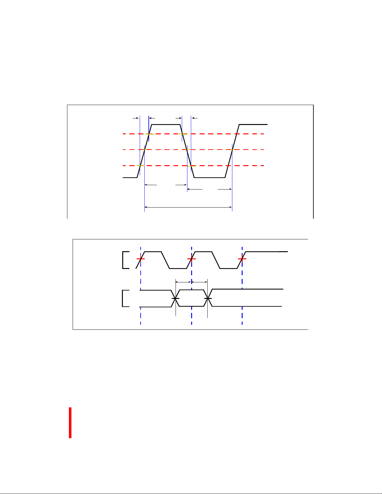
A 80960JD
TCK
TMS
TDI
T
BSCR
T
BSCF
T
BSCH
T
BSCL
Figure 20. TCK Waveform
T
BSIS1TBSIH1
1.5V
Valid
2.0V
1.5V
0.8V
1.5V1.5V1.5V
1.5V
Figure 21. Input Setup and Hold Waveforms for T
PRELIMINARY
BSIS1
and T
BSIH1
39
Page 44

80960JD A
TCK
TDO
1.5V
T
BSOV1
Valid
T
BSOF1
Figure 22. Output Delay and Output Float Waveform for T
TCK
Non-Test
Outputs
1.5V
1.5V
T
BSOV2
1.5V
Valid
T
BSOF2
1.5V1.5V1.5V
BSOV1
AND T
1.5V
BSOF1
40
Figure 23. Output Delay and Output Float Waveform for T
and T
BSOV2
BSOF2
PRELIMINARY
Page 45

A 80960JD
TCK
T
T
BSIS2
Non-Test
Inputs
Figure 24. Input Setup and Hold Waveform for T
1.5V
Valid
BSIH2
1.5V
BSIS2
1.5V1.5V1.5V
and T
BSIH2
PRELIMINARY
41
Page 46

80960JD A
F_JF030A
5.0 BUS FUNCTIONAL WAVEFORMS
Figures 25 through 30 illustrate typical 80960JD bus transactions. Figure 31 depicts the bus arbitration
sequence. Figure 32 illustrates the processor reset sequence from the time power is applied to the device.
Figure 33 illustrates the processor reset sequence when the processor is in operation. Figure 34 illustrates the
processor ONCE sequence from the time power is applied to the device. Figures 35 and 36 also show
accesses on 32-bit buses. Tables 19 through 22 summarize all possible combinations of bus accesses across
8-, 16-, and 32-bit buses according to data alignment.
CLKIN
AD31:0
ALE
ADS
A3:2
BE3:0
WIDTH1:0
D/C
W/R
BLAST
T
aTdTr
D
ADDR
In
10 10
TiTiTaTdTrTiT
Invalid
ADDR
i
DATA Out
42
DT/R
DEN
RDYRCV
Figure 25. Non-Burst Read and Write Transactions Without Wait States, 32-Bit Bus
PRELIMINARY
Page 47

A 80960JD
CLKIN
AD31:0
ALE
ADS
A3:2
BE3:0
WIDTH1:0
D/C
W/R
TaTdTdTrTaTdTdTdT
D D
ADDR
In In Out Out Out Out
00 or 10 01 or 11 00 01 10 11
1 0
DATA DATA DATA DATA
ADDR
d
1 0
T
r
BLAST
DT/R
DEN
RDYRCV
Figure 26. Burst Read and Write Transactions Without Wait States, 32-Bit Bus
PRELIMINARY
43
Page 48

80960JD A
CLKIN
AD31:0
ALE
ADS
A3:2
BE3:0
WIDTH1:0
D/C
W/R
TaTwTwTdTwTdTwTdTwTdT
ADDR
DATA
Out Out
0 0
DATA DATADATA
0 1 1 0 1 1
1 0
Out
Out
r
44
BLAST
DT/R
DEN
RDYRCV
F_JF032A
Figure 27. Burst Write Transactions With 2,1,1,1 Wait States, 32-Bit Bus
PRELIMINARY
Page 49

A 80960JD
CLKIN
AD31:0
ALE
ADS
A3:2
BE1
/A1
BE0/A0
WIDTH1:0
D/C
W/R
TaTdTdTrTaTdTdTdT
D
ADDR
D
In In Out Out
00,01,10 or 11 00,01,10 or 11
00
01 or
11
00 or 10
ADDR
DATA DATA
DATA
Out
00 01 10 11
00
T
d
r
DATA
Out
BLAST
DT/R
DEN
RDYRCV
Figure 28. Burst Read and Write Transactions Without Wait States, 8-Bit Bus
PRELIMINARY
F_JF033A
45
Page 50

80960JD A
CLKIN
AD31:0
ALE
ADS
A3:2
BE1/A1
BE3
/BHE
BE0/BLE
WIDTH1:0
D/C
TwTdTdTrTrTaTwTdT
T
a
D
ADDR
00,01,10, or 11 00,01,10, or 11
0
D
In
1
01 01
ADDR
DATA DATA
Out OutIn
0 1
T
d
r
46
W/R
BLAST
DT/R
DEN
RDYRCV
F_JF034A
Figure 29. Burst Read and Write Transactions With 1, 0 Wait States
and Extra Tr State on Read, 16-Bit Bus
PRELIMINARY
Page 51

A 80960JD
CLKIN
AD31:0
ALE
ADS
A3:2
BE3:0
WIDTH1:0
D/C
W/R
TaTdTrTaTdTrTaT
D
A AA
In
00 00 01 10
1 1 0 1 0 0 1 1
D
A
In
0 0 0 0
1 0
Valid
TrTaTdT
d
D
In
1 1 1 0
r
D
In
BLAST
DT/R
DEN
RDYRCV
Figure 30. Bus Transactions Generated by Double Word Read Bus Request,
Misaligned One Byte From Quad Word Boundary, 32-Bit Bus, Little Endian
PRELIMINARY
47
Page 52

80960JD A
the processor deasserts HOLDA on the same edge in which it recognizes the deassertion of HOLD.
Ti or T
∼
Valid
∼
∼
∼
∼
∼
∼
∼
(Note)
∼
∼
CLKIN
Outputs:
AD31:0,
ALE, ALE
ADS
WIDTH/HLTD1:0,
DT/R,
BLAST
NOTE: HOLD is sampled on the rising edge of CLKIN. The processor asserts HOLDA to grant the bus on the
same edge in which it recognizes HOLD if the last state was T
D/C
, LOCK
HOLDA
, A3:2,
BE3:0,
, W/R,
DEN,
HOLD
,
Figure 31. HOLD/HOLDA Waveform For Bus Arbitration
T
r
h
T
h
∼
∼
∼
∼
∼
∼
∼
∼
or the last Tr of a bus transaction. Similarly,
i
Ti or T
a
Valid
48
PRELIMINARY
Page 53
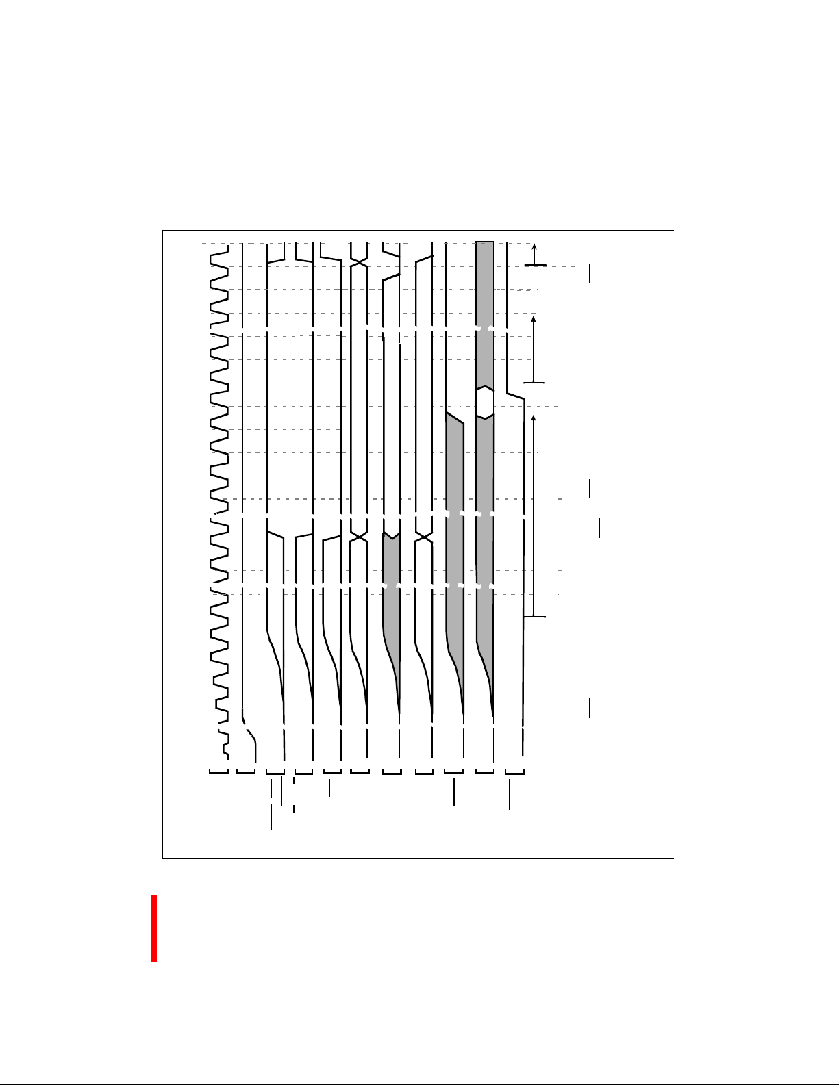
A 80960JD
CLKIN
ALE, ADS,
ALE,W/R,
RESET
LOCK/
STEST
V
CC
DT/R
FAIL
First
Bus
Activity
Valid
(Output)
ONCE
AD31:0, A3:2,D/C
WIDTH/HLTD1:0
(Note 1)
Idle (Note 2)
HOLD
Valid Input (Note 3)
BE3:0, DEN,
BLAST
Valid Output (Note 3)
HOLDA
V
10,000 CLKIN periods, for PLL stabilization.
CC
and CLKIN stable to RESET High, minimum
Built-in self-test, approximately
207,000 CLKIN periods
(if selected)
(Input)
1. The processor asserts FAIL during built-in self-test. If self- test passes, the FAIL pin is deasserted.The processor also asserts FAIL
during the bus confidence test. If the bus confidence test passes, FAIL is deasserted and the processor begins user program execution.
Notes:
2. If the processor fails built-in self-test, it initiates one dummy load bus access. The load address indicates the point of self-test failure.
3. Since the bus is idle, hold requests are honored during reset and built-in self-test.
∼
∼
∼
∼∼∼
∼
∼
∼
∼∼∼
∼
∼
∼
∼∼∼
∼
∼
∼∼∼
∼
∼
∼
∼
∼∼∼
∼
∼
∼∼∼
∼
∼
∼
∼∼∼∼∼∼∼
∼
∼∼∼
∼
∼
∼∼∼
∼
∼
∼
∼
∼∼∼
∼∼∼
∼∼∼
∼
∼
∼
∼
∼
∼
∼
∼
∼
∼
∼∼∼
∼∼∼
∼∼∼
∼∼∼
∼
∼
∼
∼
∼
∼
∼
∼
∼
∼
∼
∼
∼
∼
∼
∼
∼
∼
∼
∼
∼
Figure 32. Cold Reset Waveform
∼
∼
∼
PRELIMINARY
∼
∼
∼
∼
∼
∼
∼
49
Page 54

80960JD A
Maximum RESET Low to Reset State
4 CLKIN Cycles
CLKIN
AD31:0, A3:2, D/C
STEST
RESET
RESET High to First Bus
Minimum RESET Low Time
15 CLKIN Cycles
HOLDA
Valid
ALE, ADS, BE3:0,
DEN, BLAST
ALE, W/R,DT/R, BSTAT,
WIDTH/HLTD1:0
FAIL
HOLD
LOCK/ONCE
Activity, 46 CLKIN Cycles
∼
∼
∼
∼
∼
∼
∼
∼
∼
∼
∼
∼
∼
∼
∼∼∼
∼
∼∼∼
∼∼∼
∼
∼
∼∼∼
∼
∼
∼
∼
∼
∼∼∼
∼
∼
∼
∼
∼∼∼
∼
∼
∼
∼
∼∼∼
∼
∼
∼
∼∼∼
∼
∼
∼
∼
∼
∼
∼
∼
∼
∼
∼
Figure 33. Warm Reset Waveform
50
PRELIMINARY
Page 55
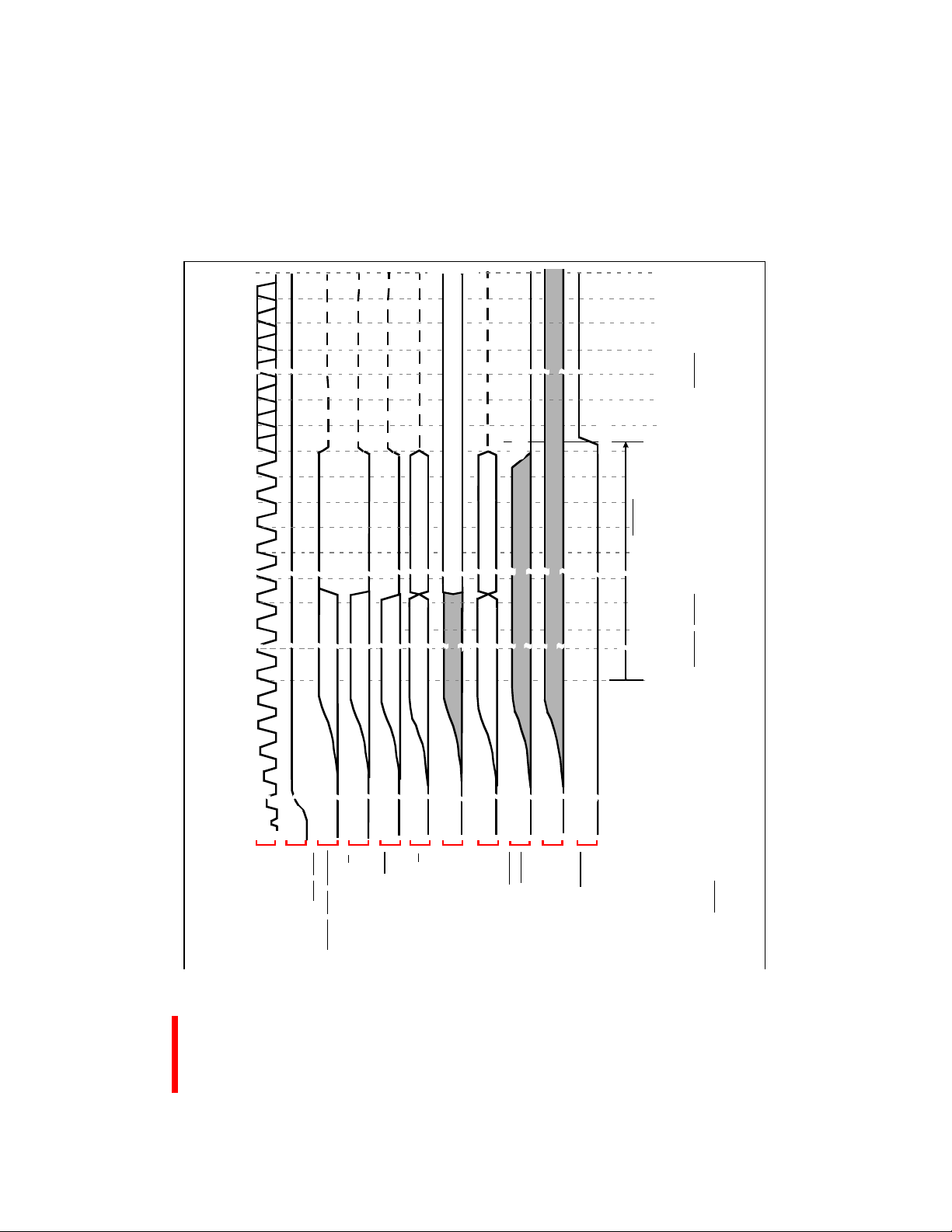
A 80960JD
CLKIN
ALE, ADS,
ALE,W/R,
RESET
LOCK/
V
CC
DT/R, WIDTH/HLTD1:0
FAIL
ONCE
AD31:0, A3:2,
D/C
HOLD
BE3:0, DEN, BLAST
HOLDA
(Input)
minimum 10,000 CLKIN periods, for PLL
V
CC
and CLKIN stable to RESET High,
(Note 1)
1. ONCE mode may be entered prior to the rising edge of RESET: ONCE input is not latched until the rising edge of RESET.
NOTES:
CLKIN may not be allowed to float.
STEST
2. The ONCE input may be removed after the processor enters ONCE Mode.
stabilization.
It must be driven high or low or continue to run.
∼
∼
∼∼∼
∼
∼
∼
∼
∼
∼
∼∼∼
∼∼∼
∼
∼
∼
∼
∼∼∼
∼
∼∼∼
∼
∼
∼
∼
∼
∼
∼∼∼
∼∼∼
∼
∼
∼
∼
∼
∼
∼
∼
∼
∼
∼
∼
∼
∼
∼
∼
∼
∼
∼
∼
∼
∼∼∼
∼
∼
∼
∼
∼∼∼
∼
∼
∼
∼∼∼
∼
∼
∼
∼
∼
∼
∼∼∼
∼
∼∼∼
∼
∼
∼∼∼
∼
∼
∼
∼
∼
∼∼∼∼∼
∼∼∼
∼
∼
∼
∼
∼
∼
∼
∼
∼
∼
∼
∼
Figure 34. Entering the ONCE State
PRELIMINARY
51
Page 56

80960JD A
Table 19. Natural Boundaries for Load and Store Accesses
Data Width Natural Boundary (Bytes)
Byte 1
Short Word 2
Word 4
Double Word 8
Triple Word 16
Quad Word 16
Table 20. Summary of Byte Load and Store Accesses
Address Offset from
Natural Boundary
(in Bytes)
+0 (aligned) • byte access • byte access • byte access
Address Offset from
Natural Boundary
(in Bytes)
+0 (aligned) • burst of 2 bytes • short-word access • short-word access
+1 • 2 byte accesses • 2 byte accesses • 2 byte accesses
Accesses on 8-Bit Bus
(WIDTH1:0=00)
Table 21. Summary of Short Word Load and Store Accesses
Accesses on 8-Bit Bus
(WIDTH1:0=00)
Accesses on 16 Bit Bus
(WIDTH1:0=01)
Accesses on 16 Bit Bus
(WIDTH1:0=01)
Accesses on 32 Bit Bus
Accesses on 32 Bit Bus
(WIDTH1:0=10)
(WIDTH1:0=10)
52
PRELIMINARY
Page 57

A 80960JD
Table 22. Summary of n-Word Load and Store Accesses (n = 1, 2, 3, 4)
Address Offset
from Natural
Boundary in Bytes
+0 (aligned)
(n =1, 2, 3, 4)
+1 (n =1, 2, 3, 4)
+5 (n = 2, 3, 4)
+9 (n = 3, 4)
+13 (n = 3, 4)
+2 (n =1, 2, 3, 4)
+6 (n = 2, 3, 4)
+10 (n = 3, 4)
+14 (n = 3, 4)
+3 (n =1, 2, 3, 4)
+7 (n = 2, 3, 4)
+11 (n = 3, 4)
+15 (n = 3, 4)
+4 (n = 2, 3, 4)
+8 (n = 3, 4)
+12 (n = 3, 4)
Accesses on 8-Bit Bus
(WIDTH1:0=00)
• n burst(s) of 4 bytes • case n=1:
• byte access
• burst of 2 bytes
• n-1 burst(s) of 4 bytes
• byte access
• burst of 2 bytes
• n-1 burst(s) of 4 bytes
• burst of 2 bytes
• byte access
• n-1 burst(s) of 4 bytes
• burst of 2 bytes
• byte access
• n burst(s) of 4 bytes • n burst(s) of 2 short words • n word access(es )
Accesses on 16 Bit Bus
(WIDTH1:0=01)
burst of 2 short words
• case n=2:
burst of 4 short words
• case n=3:
burst of 4 short words
burst of 2 short words
• case n=4:
2 bursts of 4 short words
• byte access
• short-word access
• n-1 burst(s) of 2 short words
• byte access
• short-word access
• n-1 burst(s) of 2 short words
• short-word access
• byte access
• n-1 burst(s) of 2 short words
• short-word access
• byte access
Accesses on 32 Bit
Bus (WIDTH1:0=10)
• burst of n word(s)
• byte access
• short-word access
• n-1 word access(es)
• byte access
• short-word access
• n-1 word access(es)
• short-word access
• byte access
• n-1 word access(es)
• short-word access
• byte access
PRELIMINARY
53
Page 58

80960JD A
Byte Offset
Word Offset
Short-Word
Load/Store
Word
Load/Store
0 4 8 12 16 20 24
0 1 2 3 4 5 6
Short Access (Aligned)
Byte, Byte Accesses
Short Access (Aligned)
Byte, Byte Accesses
Word Access (Aligned)
Byte, Short, Byte, Accesses
Short, Short Accesses
Byte, Short, Byte Accesses
One Double-Word Burst (Aligned)
Byte, Short, Word, Byte Accesses
54
Double-Word
Load/Store
Short, Word, Short Accesses
Byte, Word, Short, Byte Accesses
Word, Word Accesses
One Double-Word
Burst (Aligned)
Figure 35. Summary of Aligned and Unaligned Accesses (32-Bit Bus)
PRELIMINARY
Page 59
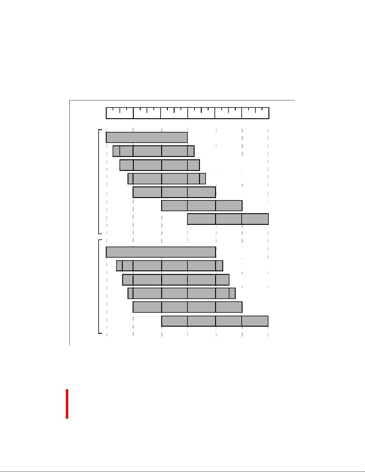
A 80960JD
Byte Offset
Word Offset
Triple-Word
Load/Store
Quad-Word
Load/Store
0 4 8 12 16 20 24
0 1 2 3 4 5 6
One Three-Word
Burst (Aligned)
Byte, Short, Word,
Word, Byte Accesses
Short, Word, Word,
Short Accesses
Byte, Word, Word,
Short, Byte Accesses
Word, Word,
Word Accesses
Word, Word,
Word Accesses
One Four-Word
Burst (Aligned)
Byte, Short, Word, Word,
Word, Byte Accesses
Short, Word, Word, Word,
Short Accesses
Byte, Word, Word, Word,
Short, Byte Accesses
Word,
Word,
Word
Accesses
Figure 36. Summary of Aligned and Unaligned Accesses (32-Bit Bus) (Continued)
PRELIMINARY
Word, Word, Word,
Word Accesses
Word,
Word,
Word,
Word,
Accesses
55
Page 60

80960JD A
6.0 DEVICE IDENTIFICATION
80960JD processors may be identified electrically according to device type and stepping (see Table 23). The
32-bit identifier is accessible in three ways:
• Upon reset, the identifier is placed into the g0 register.
• The identifier may be accessed from supervisor mode at any time by reading the DEVICEID register at
address FF008710H.
• The IEEE Standard 1149.1 Test Access Port may select the DEVICE ID register through the IDCODE
instruction.
The device and stepping letter is also printed on the top side of the product package.
Table 23. 80960JD Die and Stepping Reference
Device and
Stepping
Version
Number
Part Number Manufacturer X
Complete ID
(Hex)
80960JD A, A2 0000 1000 1000 0010 0000 0000 0001 001 1 08820013
NOTE: This data sheet applies to the 80960JD A and 80960JD A2 steppings.
7.0 REVISION HISTORY
This data sheet supersedes revision 272596-001. Table 24 indicates significant changes since the previous
revision.
Table 24. Data Sheet Version -001 to -002 Revision History (Sheet 1 of 2)
Table 13, 80960JD DC Characteristics (pg. 24) Removed Icc characteristics. Added V
ground bounce) specification
Table 14, 80960JD ICC Characteristics (pg.
25)
New table for comprehensible Icc characteristics.
Added Icc’s for reset mode. Halt Icc for: 80960JD-50
OLP
(output
(max) improved from 56 mA to 48 mA, 80960JD-40
(max) improved from 44 mA to 41mA. ONCE Icc
Improved from 30 mA to 10 mA.
Section 4.5, AC Specifications (pg. 26) Grouped AC Specifications tables by frequency. Added
40 MHz and 33 MHz AC specifications.
(max) improved from ±0.1% to ±250 ps
Table 15, 80960JD AC Characteristics (50
MHz) (pg. 26) Section INPUT CLOCK
T
CS
TIMINGS
(min) improved from 3.0 ns to 3.5 ns. T
Table 15, 80960JD AC Characteristics (50
MHz) (pg. 26) Section SYNCHRONOUS
OUTPUT TIMINGS
56
T
ov1
improved from 0.45T
+ 3.0 ns to 0.5TC + 3.5 ns. ToF
C
(min) improved from 3.0 ns to 3.5 ns. T
improved from 17 ns to 15 ns.
PRELIMINARY
(max)
oF
ov2
(min)
Page 61

80960JD A
Table 24. Data Sheet Version -001 to -002 Revision History (Sheet 2 of 2)
Table 15, 80960JD AC Characteristics (50
MHz) (pg. 26) Section SYNCHRONOUS
INPUT TIMINGS
Table 15, 80960JD AC Characteristics (50
MHz) (pg. 26) Section RELATIVE OUTPUT
TIMINGS
Table 15, 80960JD AC Characteristics (50
MHz) (pg. 26) Section BOUNDARY SCAN
TEST SIGNAL TIMINGS
T
(min) improved from 10 ns to 9 ns
IS2
, T
T
LXL
to .5T
T
BSF
improved from 8 ns to 4 ns. T
, and T
LXA
- 7.5 ns.
C
(max) improved from 8 MHz to .5TF. T
10 ns to 6 ns. T
(min) improved from 10 ns to 6 ns.
T
BSIH2
(min) improved from .45TC - 3 ns
DXD
BSIH1
(min) improved from 8 ns to 4 ns.
BSIS2
(min)
(min) improved from
BSIS1
57
PRELIMINARY
 Loading...