

Page 1

536EX Chipset
Developer’s Manual
January 2002
Order Number: 273584-002
Page 2

Information in this document is provided in connection with Intel® products. No license, express or implied, by estoppel or otherwise, to any intellectual
property rights is granted by this document. Except as provided in Intel’s Terms and Conditions of Sale for such products, Intel assumes no liability
whatsoever, and Intel disclaims any express or implied warranty, relating to sale and/or use of Intel products including liability or warranties relating to
fitness for a particular purpose, merchantability, or infringement of any patent, copyright or other intellectual property right. Intel products are not
intended for use in medical, life saving, or life sustaining applications.
Intel may make changes to specifications and product descriptions at any time, without notice.
Designers must not rely on the absence or characteristics of any features or instructions marked “reserved” or “undefined.” Intel reserves these for
future definition and shall have no responsibilit y wha tsoeve r for conflicts or incompat ibilities arisi ng from futu re changes to them.
The 536EX may contain design defects or errors known as errata which may cause the produc t to deviate from publishe d specificat ions. Current
characterized errata are available on request.
Contact your local Intel sales office or your distributor to obtain the latest specifications and befo re placi ng your product order.
Copies of documents which have an ordering number and are referenc ed in this docume nt, or other In tel literature may be obtained by callin g
1-800-548-4725 or by visiting Intel's website at http://ww w.intel.com.
Copyright © Intel Corporation, 2002
*Third-party brands and names are the property of their respective owne rs.
2 536EX Chipset Developer’s Manual
Intel Confidential
Page 3

Contents
Contents
1 Introduction......................................................................................................................................7
1.1 Controllerless Modem Driver Overview................................................................................7
1.1.1 Windows* M ill ennium Edition (Windows Me), Windows 2000, Windows XP, and
Windows NT* 47
1.1.2 Windows 95 and Windows 98..................................................................................8
1.2 V.90/V.92 and V.34 Data Modes... ................ .............................. ................. ........................9
1.3 Modem Connection Overvie w..................... ........................................... .............................10
1.4 AT Commands Overview....................................................................................................11
1.4.1 Se n din g Co mmands.. ... .............................. .............................. ................. ............12
1.4.2 AT Esca p e Sequen ce s..... .............................. ................ .............................. .........13
1.4.3 D i al Modifi e r.................. .... .............................. ................ .............................. .........13
2 AT Command Summary Tables....................................................................................................14
3 Data Mode AT COMMANDS.........................................................................................................26
3.1 Using AT Commands to Access the S-Registers [Sn?, Sn=x, ?]........................................26
3.2 Modem Responses and Comman d Echo [En , Vn, Xn, Wn, Qn]......... ... .............................26
3.3 Modem Reset and NVRAM Commands [DS=m, Zn, &F, &Vn, &Yn, &Wn, &Zn=x]...........28
3.4 Modem Identificatio n Commands [In, +F MI, +FMR, +F MM, +GMI, +GMM, +GMR, +GSN,
+FMFR?, +FMDL?, +FREV?].............................................................................................29
3.5 Establishing a Modem Connection [A, D, DS = n, S0]........................................................29
3.6 Online Command Mode [Escape Codes , On]........................ ................ .............................30
3.7 Hanging Up [Hn, S10, Zn, &D2]..........................................................................................30
3.8 Modem-to-Modem Connec ti o n Data Rates.............................. .............................. ............30
3.9 Diagnostic Testing [S18, &Tn]............................................................................................36
3.9.1 L oc al An alo g Loopb ac k [AT&T 1]... ... ................. .............................. ......................36
3.9.2 Local Analog Loopback With Self-Test [AT&T8]....................................................37
3.10 AT Escape Sequences .......................................................................................................38
3.10.1 Time-Independen t Esc ape Sequ en ce .......................................... ................ .........38
3.10.2 Hayes* Escape Sequence.............................. .............................. .........................40
4 Error Correctio n and Data Compre ssio n.. ........................................... .............................. ............56
5 Fax Class 1 AT Commands...........................................................................................................64
5.1 Fax Identity Commands......................................................................................................64
5.2 Fax Class 1 Commands .....................................................................................................64
6 IS-101 Voice Mode AT Commands...............................................................................................70
6.1 DTMF Detection Reporting.................................................................................................71
6.2 Relay Control......................................................................................................................71
7 S-Registers....................................................................................................................................85
8 Caller ID.........................................................................................................................................90
9 Parallel Host Interfa ce 16C45 0 /1 6C55 0A UART................ .... ........................................... ............92
9.1 UART Emulation in the Controllerless Modem...................................................................92
9.2 UART Register Definitions.................................................................................................. 95
536EX Chipset Developer’s Manual 3
Intel Confidential
Page 4

Contents
9.2.1 Scratch Register (SCR).........................................................................................95
9.2.2 Modem Status Register (MSR)..............................................................................95
9.2.3 Line Status Register (LSR).................................................................................... 9 6
9.2.4 Modem Control Register (MCR)............................................................................9 7
9.2.5 Line Control Register (LCR)..................................................................................97
9.2.6 FIFO Control Register (FCR)................................................................................. 9 8
9.2.7 Interrupt Identity Register (IIR)....................................... .............................. .........99
9.2.8 Interrupt Enable Register (IER) ...........................................................................100
9.2.9 Transmitter Holding Register (THR)....................................................................100
9.2.10 Receiver Buffer Register (RBR)...........................................................................101
9.2.11 Divisor Latch Registers (DLM and DLL)..............................................................101
9.3 16C550A UART FIFO Operation ......................................................................................102
9.3.1 FIFO Interrupt Mode Operati o n........ ... ................. .............................. .................102
9.3.2 FIFO Polled Mode Operation...............................................................................102
Figures
1 WDM Driver Block Diagram........ .............................. .............................. ......................................8
2 VxD Mini Port Driver Block Diagram.............................................................................................9
3 Example of a Remote Connection..............................................................................................27
4 Modem-on-Hold: Incoming Voice Call in Data Mode..................................................................32
5 Modem-on-Hold: Initiating a Voice Call in Data Mode................................................................33
6 Local Analog Loopback Test......................................................................................................3 7
7 Local Analog Loopback with Self-Test .......................................................................................3 7
8 T.30 HDLC Frame Format..........................................................................................................66
9 CLASS 1 DTE-Generated HDLC Frame Information (AT+FTH=<mod>)...................................6 6
10 CLASS 1 DTE Reception of HDLC Frame Information (AT+FRH=<mod>) ...............................66
11 UART Emulation in Intelsdb.VxD................................................................................................92
12 FIFO Buffers for Transmitter and Receiver ................................................................................93
13 Parallel Host Interface UART Register Bit Assignments............................................................94
14 Scratch Register (SCR)..............................................................................................................95
15 Modem Status Register (MSR)...................................................................................................95
16 Line Status Register (LSR).........................................................................................................9 6
17 Modem Control Register (MCR).................................................................................................97
18 Line Control Register (LCR).......................................................................................................9 7
19 FIFO Control Register (FCR)...................................................................................................... 9 8
20 Interrupt Identity Register (IIR)...................................................................................................9 9
21 Interrupt Enable Register (IER) ................................................................................................100
22 Transmitter Holding Register (THR).........................................................................................100
23 Receiver Buffer Register (RBR) ............................................................................................... 101
24 Divisor Latch Registers (DLM and DLL)...................................................................................101
4 536EX Chipset Developer’s Manual
Intel Confidential
Page 5

Contents
Tables
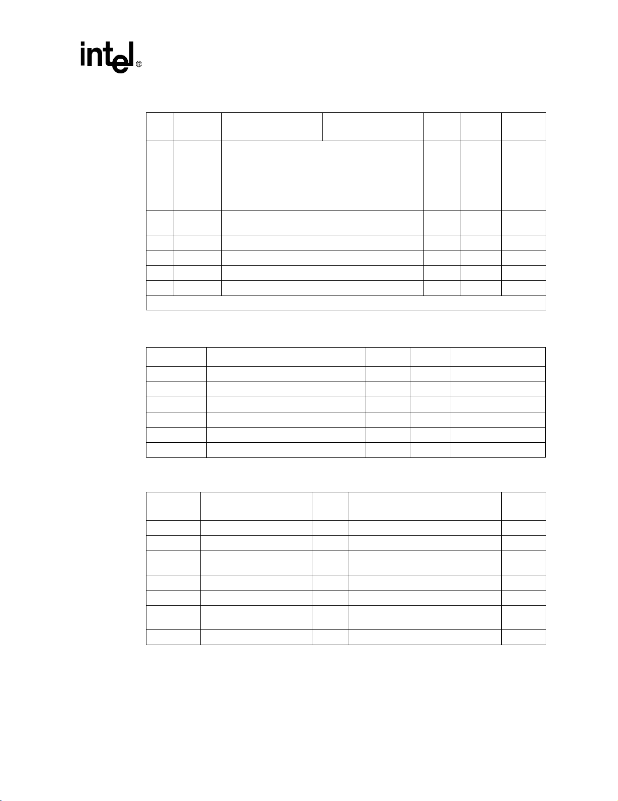
1 DTE-to-DCE Data Rates for Each Mode....................................................................................11
2 DCE-to-DCE Data Rates for Each Mode....................................................................................11
3 DCE-to-ISP Data Rates for V.90 Mode......................................................................................11
4 DTE-Modem Data Rate Response Codes... .............................. ............................................ .....12
5 Data Mode Command Summary................. .............................. ................. .............................. ..14
6 V.44/V.42/V.42 bis MNP Command Summary...........................................................................19
7 Fax Identity Command Summary...............................................................................................21
8 Fax Class 1 Command Summary...............................................................................................21
9 IS-101 Voice Command Summary.............................................................................................22
10 Voice DTEÆDCE Character Pairs..................... .............................. .............................. ............22
11 Voice DTE¨DCE Character Pair s........... ................ .............................. .............................. .........23
12 Dial Modifiers......................................... .............................. ................ .......................................24
13 S-Register Summary ..................................................................................................................24
14 Data Reporting Wn Mapping ......................................................................................................27
15 Product Identifica tion Inf ormat i on.................... ................ ................. .............................. ............29
16 Supported Modulation Types......................................................................................................35
17 Resulting Modem-to-Modem Connection Rates with Non-Default Values .................................36
18 Data Mode Command Description s............. ................. .............................. .............................. ..40
19 Operating Modes........................................................................................................................56
20 Resulting +ES Connection Types...............................................................................................57
21 V.44/V.42/V.42 bis and MNP Data Modem Command Descriptions ..........................................57
22 Fax Identity Command Descriptions...........................................................................................64
23 <mod> Selection Table ...............................................................................................................65
24 Fax Mode Command Descriptions ............................................................................................. 67
25 Voice Mode Command Descriptions ..........................................................................................71
26 S-Register Command Descriptions............................................................................................85
27 Caller ID Tags for Formatted Reporting......................................................................................90
28 Interrupt Control Functions.........................................................................................................99
29 Programmable Data Rates.......................................................................................................101
536EX Chipset Developer’s Manual 5
Intel Confidential
Page 6

Contents
Revision History
Date Revision Description
January 2002 002
August 2001 001 Initial release
Changed references to “HaM Data Fax Voice” to “Intel 536EP
V.92 Modem.”
6 536EX Chipset Developer’s Manual
Intel Confidential
Page 7

Introduction 1
This developer’s manual describes the software interface for Intel® 536EX (controllerless and
controll e r) chipset solu tions. The controllerless-b a sed solutions include the 536EP for PCI and
Mini-PCI. Re fer to the chipse t da tasheets for the detailed chipset descriptions (public order
numbers 273503-001, 273xxx-001, 273 xxx-001, 273xxx-001, and 273xxx-001).
The controllerless-bas ed chi ps et, as the name implies, does not have a dedicated hardware
controller . The control ler functi ons are execu ted by th e CPU. This deve loper’ s man ual inclu des the
AT command sets for da ta, fax, and voice and the UAR T interface and emulation. Like the earlier
solutions from Intel, the 536E X chipsets support a variety of applications without the need of
additional firmware de velopment. Note, the supported AT commands are firmware or driver
version dependent.
1.1 Controllerless Modem Driver Overview
1.1.1 Windows* Millennium Edition (Windows Me), Windows 2000, Windows XP, and Windows NT* 4
The controllerless modem chipsets are integrated into the Microsoft* Windows* Me, Windows
2000, Windows XP, and Windows NT* 4 operating systems via proprieta ry Intel® Windows
Driver Model (WDM) modem drivers. These driver s are fully plug and play capable and conform
to all Microsoft WHQL certification requirements.
The funct i on a l blo c k di a g ra m in Figure 1 shows the common WDM architecture for the
Microsof t’s operating systems supporting c ommon WDM drivers model.
User-mode applic ation, via special W indows API (FILE, T API, UNIMODEM), can access a virtual
COM port prov ided by the Intel WDM driver. T he da ta flow is conver te d inside the driver in
accordance with some compressio n and a channel level protocol and passed to the DSP. The
control flow fo llows the common Micros oft WDM driver model. The Intel WDM driver is
installed as a stack of filter dri ver s be low the system modem.sys driver.
536EX Chipset Developer’s Manual 7
Intel Confidential
Page 8
Introduction
Figure 1. WDM Driver Block Dia g ram
applications
User applications
virtual COM
protocols
User
Kernel - ring0
Modem drivers stack
port,
channel
layer
WDM driver
Intels51.sys
PCI bus
Hardware
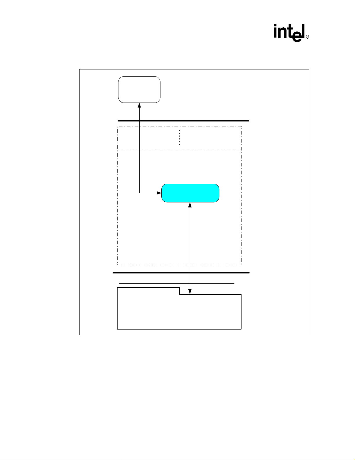
1.1.2 Windows 95 and Windows 98
When the controllerless modem chipsets are used with Microso ft Windows 95 and Windows 98
applications, the traditional UART and serial port emulations are replaced by the propri etary HaM
Mini Port driver (see Figure 2). Instead of transferring commands to UART vir tual registers, then
to a serial port, the HaM Port Driver sends commands directly to the Windows virtual machine
driver VCOMM. VxD. This low-level communication driver supports the Win16 and Win32
Communication APIs. Like the WDM drivers, the Mini Port VxD drivers are fully plug and play
and conform to Microsoft WHQL certification requirements.
8 536EX Chipset Developer’s Manual
Intel Confidential
Page 9
When the controllerle ss chipsets are used with MS-DOS* applications, however, a UART
emulation is required. Intel provides an additional driver called Intelsdb.VxD, which includes a
UAR T em ulation. Please refer to Section 9.1, “UAR T Em ulation in the Controllerless Modem” on
page 92 for an explanation of the 536EX UART emulation. The Intelsdb.VxD driver interacts
directly with the VCOMM.VxD dr iver using the Win16 and Win32 Communi c a tion APIs.
Figure 2. V xD Mini Port Driver B lock Dia gram
NON-SYSTEM
VIRTUAL MACHINE
MS-DOS SHELL APPLICATION
OR DRIVER
Introduction
SYSTEM VIRTUAL MACHINE
MS-DOS
APPLICATION
Intelsdb.VXD
WINDOWS
APPLICATION
TAPI
Unimodem COMM.DRV
VCOMM.VXD
HaM Port Driver
Interrupt Services
Chipset Hardware
Win 16
1.2 V.90/V.92 and V.34 Data Modes
The 536EX chipset defaults to the V.90 or V.92 mode depending on the driver version. The V.90/
V.92 mode allows receive data rates of up to 56,000 kbps over the PSTN (public switched
telephon e network) only in connections with equipment-compatible ISPs (Internet Service
Providers); howev e r, FCC regulations limit receive speeds to 53,333 kbps due to excessive power
demands at higher speeds. In modem-to-modem connections, V.90/V.92 mode falls back to V.34
mode in both the transmit and receive directions. The chipsets implement all data rates and
modulation schemes for ITU-T (International Telecommunications Union-Telecommunications)
standards V.34, V.32 bis, V.32, V.22 bis, V.22, V.21, Bell 212A, and Bell 103.
536EX Chipse t D eveloper’s Manua l 9
Intel Confidential
Page 10

Introduction
1.3 Modem Connection Overview
The DCE (modem) operates in one of two states: command or online. In each state, both data and
commands (i nc luding DCE res ponses) are transferred through the UART THR (Transmit Holdi ng
register) and the RBR (Receiver Buffer register).
The modem defaults to the command state. I n the command stat e, the DTE (host) communica tes to
the modem through AT commands and S-registers. AT commands are character strings that help
guide modem operation. S-r e gisters are internal modem registers that the DT E can access. The Sregisters contain mode m st a t us and configuration information. Many of the AT commands
indirectly affect the contents of the S-registers. The AT command set and S-registers are divided
into the following modes: Group 3 fax, data, V.44/V.42 bis/V.42/MNP, and voice. Note that
supported AT commands ar e fi rmwar e r evis io n-dep ende nt ( that is , not a ll comma nds are suppo rt ed
by all modem models or all firm ware revisions).
All command lines sent to the modem , except for A/, must be preceded by an ‘AT’ (which stands
for ‘attention’) and terminated by the contents of S-register S3 (typically a carriage return <CR>).
The ‘AT’ prompts the modem to receive a com man d line from the DTE. A <CR> informs the
modem that the entire command string has been trans mitted and that the modem sho uld start
processing all the commands wit hin the command line.
A command line may include one or more AT commands that may or may not be separate d by a
space. AT commands may be either upper- or lower-case characters, but all characters for a given
command must use the same cas e. If t here ar e mult iple co mmands in a li ne, a sem icolo n (;) must b e
placed after each fax or voice command. The modem can be configured to send back (echo) to the
DTE any data that the DTE sends to the mo dem (while in command state only). The last comm and
may be repeated by typing A/ witho ut using a carriage return. Each command line may include up
to 80 characters and spaces.
Examples of AT command strings:
ATS1?<CR>
A/
AT &C1 &D2 +FCLASS=? <CR>
AT &C1 &D2 +FCLASS=?; S0=1 <CR>
The modem provides status infor mat ion to the DTE in the form of response code s. These response
codes can be expressed in text or numeric form. The support e d response codes are provided in
T a ble 4 on page 12.
Examples of mo de m responses:
+MCR: V90
+MRR: 28800
CONNECT 50666
In the online state, the DCE is off-hook and communicating with a remote modem. Any data sent
from the DTE to the DCE is transmitted to the remote modem. Similarly, any data that the DCE
receives from the remote modem is transmitted to the DTE.
Note: In the online state, the DCE does not ‘echo-back’ any of the data that the DTE sent to the DCE.
10 536EX Chipset Developer’s Manual
Intel Confidential
Page 11

The mode m rec ogn ize s AT comman ds f r om th e D TE at any val id data ra te f rom 30 0 bps t o 115,200
bps (that is, the modem autobau ds up to 115,200 bps); however, the DTE should use the data r a te
specified for each mode according to the transmitting dir ection—DTE-to-modem (Table 1) or
modem-to-modem (Table 2). The V.90 and V .92 data rates are effective only in DCE-to- IS P
connections.
T able 1. DTE-to-DCE Data Rates for Each Mode
Mode Data Rate (bps) Affected Data
Data (V.34) 2400–115,200
Data (V.92) 28,800–115,200
Fax 19,200
Voice 19,200–115,200
Table 2. DCE-to-DCE Da ta Rates for Each M o d e
Mode Data Rate (bps) Affected Data
Introduction
DTE-to-modem data rate Data (V.90) 28,800–115,200
AT commands, playback and record modes
(varies according to compression type)
Data (V.34)
(transmit and receive)
Fax 300–14,400
Voice 19,200–115,200
2400–33,600
T able 3. DCE-to-ISP Data Rates for V.90 Mode
Mode Data Rate (bps) Affected Data
Data (V.90) transmit 4800–33,600
Data (V.90) receive 28,000–56,000
Data (V.92) transmit 24,000–48,000
Data (V.92) receive 28,000–56,000
Each comma nd ma y ha ve on e or mo re p aram et ers ass oci ated w ith it. If a pa ram eter is not se nt f or a
command requiring a numeric parameter, then the mod em ass ume s a zero (‘0’) parameter (only if
zero is a valid parameter for the command ). Fo r example, ATZ and ATZ0 commands perform
identical functi ons (that is, the modem sees ‘ATZ’ and automatically uses the ‘0’ param e ter during
processi ng the command). Other commands do not us e pa rameters.
1.4 AT Commands Overview
DTE-to-modem data rate
AT commands, playback and record modes
(varies according to compression type)
ISP-to-modem data rate
The AT command set and S-registers are divided into fo ur categori es: data , Group 3 fax, voice, and
V.42/MNP. Summaries of all commands are provided later on in this ch apter.
536EX Chipset Developer’s Manual 11
Intel Confidential
Page 12

Introduction
1.4.1 Sending Commands
All command lines sent to the modem, except for A/, must be preceded by an ‘AT’ and terminated
by the contents of S-register S3 (typically a carriage return <CR>). AT stands for ‘attention’ and
prompts the modem to receive a command line from the DTE. A <CR> informs the modem that the
entire command string has been transmitted and to begin processing all the commands in the
command line. A command line can include one or more AT commands. The commands can be
separated by a space, if desired, but no punctuation is needed except for extended commands.
Extended commands begin with a ‘+’, such as fa x, voice, and V.250 commands. In a multiplecommand line, extended AT commands must be separated from following commands by a
semicolon(;).
Examples:
ATS1?<CR>
A/
AT &F &D2 +FCLASS=?<CR>
AT +FCLASS=0; S0=1<CR>
The modem provides status information to the DTE in the form of response codes, as listed in
Table 4. Response codes take two (2) forms, text (ATV1) or numeric (ATV0), depending on how
the modem is confi gured.
Table 4 lists basic for mat response codes. These response codes have numeric equivalents that are
displayed depending on the value of ATV. In addition to th e ba sic format response codes, there are
extended syntax result codes that in dicate connection status of the DCE-DCE connection that are
not effected by numeric response rep orting. These result codes have no numeric equivalent and are
always issued in text form. The res ult codes displ a y modem mode, transmit connection rate, error
correction, compression, DTE rate, and receive rate. Note that the final connection message only
indicates receive ra te i f ATXn is greater t han 0. The format for the re sult codes code de pends on the
Wn command. The setting of the Wn command will determine which of the following connect
results codes are disp layed ( +MCR, + MRR, +E R, + DR, +I LRR). Refe r to the Wn comm and for the
detailed description of the command. Note that the supported carrier mo des for +MCR can be
found in p arameter 1 of +MS. The last result code is the CONNECT <text>, where tex t is the DCE
receive rate. Note, the CONNECT <text> is not displayed when ATX0 is indicated, just
CONNECT is displayed and is reported by the rules in Table 4.
Table 4. DTE-Modem Da ta Rate Res po n s e Co d es
Numeric Text Numeric Text
0 OK 9 DELAYED CALL
1 CONNECT 10 BLACKLISTED
2RING11+FCERROR
3 NO CARRIER 12 RINGBACK
4ERROR13CPON=
6 NO DIALTONE 14 CPOF=
7 BUSY 15 DRON=
8 NO ANSWE R 16 DROF=
After sending an AT command string to the modem, the DTE must wait for a response code from
the modem befor e sending a new AT command strin g to the modem.
12 536EX Chipset Developer’s Manual
Intel Confidential
Page 13

1.4.2 AT Escape Sequences
The 536EX provides the industry-standard escape sequence, TIES (Time Independent Escape
Sequence). TIE S is designed to work with existing communication software writt en for the Hayes
Escape Sequence.
Upon special request, Ambient provides the Hayes* Escape Sequence; however, please note that
licensing can be required.
TIES/Hayes * Escape Sequenc e s
The 536EX modem c hipset is manufa c tured with TIES (Time Independent Escape Sequence) as
the default setti ng. It is Hayes’ position that you must have a valid license fr om Hayes Micro
Computer of Norcross, Georgia, before producing modem systems that us e the Hayes Escape
Sequence.
Intel accepts no responsibility and does not indemnify nor in any way pro vide protection for
patent or possible patent violations to its customers or users of it products.
1.4.3 Dial Modifier
Introduction
Command Function
0 to 9 Dialing digits
A, B, C, D, *, # Tone dial characters
P Pulse dial
R Reverse Originate mode
S=n Dial NVRAM telephone number
T Tone dial
W Wait for dial tone
, Pause
! Flash hook
@ Wait for quiet answer
; Return to command state
- ( ) Ignored by modem
536EX Chipset Developer’s Manual 13
Intel Confidential
Page 14

AT Command Summary Tables
AT Command Summary Tables 2
This section contains summary tables of all AT commands, S-regis ters, and bet ween AT commands
and S-regis t e rs. These commands are fully described in the rel e va nt sections of the 536EX
Developer’s Manual.
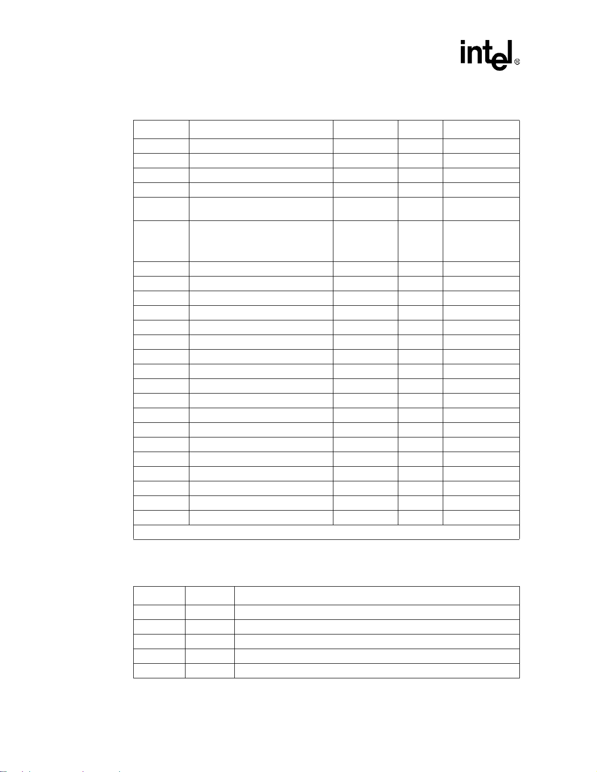
Table 5. Dat a Mode Comma nd Su mma ry
Note Command Function Default Range
** A/ Repeat last command none – no
A Answer none – no
Cn Carrier control option 1 0, 1 no
C0 Transmit carrier always off
C1 Normal transmit carrier
D Dial command none – no
* En Command mode echo 1 0, 1 yes
E0 Disables echo
E1 Enables echo
Hn Switch hook control 0 0, 1 no
H0 Hangs up the telephone line
H1 Picks up the telephone line
In Identification/checksum option 0
I0 ROM Checksum
I1 Modem Name
I2 Manufacturer
I3 Chipset
I4 Firmware Version
I5 Modem Chip Hardware Configuration
I6 DSP Patch Level
I12 Country Code
I7–I11, I13,
I14, I20–
I25
* Ln Speaker volume control 2 0–3yes
L0 Low speaker volume
L1 Low speaker volume
L2 Medium speaker volume
* Value saved in NVRAM.
** Command not preceded by an ‘AT.’
Reserved
0–7, 10–11,
14, 20–23
Reported
by &Vn
no
14 536EX Chipset Developer’s Manual
Intel Confidential
Page 15

Table 5. Data Mode Command Summary (Continued)
AT Command Summary Tables
Note Command Function Default Range
L3 High speaker volume
* Mn Speaker control 1 0–3yes
M0 Speaker always off
M1 Speaker on until carrier present
M2 Speaker always on
M3
On Go online 0 0, 1, 3 no
O0 Returns modem to Data mode
O1
O3
* P Select pulse dialing none – yes
* Qn Result code display control 0 0, 1 yes
Q0 Enables result codes
Q1 Disables result codes
Sn Select an S-register none 0–33 no
Sn=x Write to an S-register none
Sn? Read from an S-register none 0–33 no
* T Select tone dialing none – no
* Vn Result code form 1 0, 1 yes
V0 Choose numeric form
V1 Choose verbose (text) form
* Wn Response code data rate 0 0–4yes
W0, W1 DTE data rate
W2 Modulation, DCE TX rate
W3
W4
* Value saved in NVRAM.
** Command not preceded by an ‘AT.’
Speaker off during dialing; speaker on until
carrier present
Retrains equalizer and then returns to Data
mode
Renegotiates rate and then returns to Data
mode
n = 0–33
x = 0–255
Modulation, DCE TX rate, Error Correction,
Compression and DTE data rate
Modulation, DCE TX rate, Error Correction,
Compression
Reported
by &Vn
no
536EX Chipset Developer’s Manual 15
Intel Confidential
Page 16

AT Command Summary Tables
Table 5. Data Mode Command Summary (Continued)
Note Command Function Default Range
* Xn Result code type 4 0–4yes
X0
X1
X2
X3
X4
* Yn Long space disconnect 0 0, 1 yes
Y0 Disables long space disconnect
Y1 Enables long space disconnect
Zn Recall stored profile 0 0, 1 no
Z0 Resets modem and recalls user profile 0
Z1 Resets modem and recalls user profile 1
* &Cn DCD (data carrier detect) option 1 0, 1 yes
&C0
&C1 DCD set according to remote modem status
&Dn DTR (data terminal ready) option 2 0–3yes
&D0 In Async mode, modem ignores DTR
&D1
&D2
&D3
&F Load factory defaults none – no
*&Gn
&G0 Disables guard tone
&G1 Enables 550 Hz guard tone
&G2 Enables 1800 Hz guard tone
&Kn Select serial flow control 3 0, 3, 4 yes
* Value saved in NVRAM.
** Command not preceded by an ‘AT.’
Enables result c odes 0–4; disables detection
of busy and dial tone
Enables result codes 0–5, 10, and above;
disables busy and dial tone detection
Enables result codes 0–6 and 10 and above;
disables busy detection and enables dial
tone detection
Enables result codes 0–5, 7, and 10 and
above; enables busy detection and disables
dial tone detection
Enables result codes 0–7 and 10 and above;
enables busy and dial tone detection
Ignores remote modem status; DCD always
on
Modem switches from data mode to
command mode when an on-to-off transiti on
of DTR occurs
When DTR switches off, the modem goes
on-hook and disables Auto-answer mode;
when DTR switches on, auto-answer is
enabled
Turning off DTR re- initializ es the modem and
resets values except UART registers
Guard tone option (1200 bps and 2400 bps
only)
00–2yes
Reported
by &Vn
16 536EX Chipset Developer’s Manual
Intel Confidential
Page 17

Table 5. Data Mode Command Summary (Continued)
AT Command Summary Tables
Note Command Function Default Range
&K0 Disables flow control
&K3 Bidirectional hardware flow control
&K4 XON/XOFF software flow control
* &Pn Dial pulse ratio 0 0, 1 yes
&P0
&P1
* &Sn DSR (data set ready) option 0 0, 1 yes
&S0 DSR is always active
&S1
&Tn Self test commands 0 0–1, 8 no
&T0 Terminates test in progress
&T1 Initiates local analog loopback
* &Un Disable Trellis coding 0 0, 1 no
&U0 Enables Trellis coding with QAM as fallback
&U1 QAM modulation only
&Vn View active and stored profiles 0 0, 1, 3 no
&V0 View active profile and stored profile 0
&V1 View active profile and stored profile 1
&Wn Stored active profile 0 0, 1 no
&W0 Store in user profile 0
&W1 Store in user profile 1
* &Yn Select stored profile on power up 0 0, 1 yes
&Y0 Recall stored profile 0 on power-up
&Y1 Recall stored profile 1 on power-up
&Zn=x
* %En Auto-retrain control 1 0, 1 yes
%E0 Disables auto-retrain
%E1 Enables auto-retrain
* %Gn Rate renegotiation 1 0, 1 yes
%G0 Disabled
%G1 Enabled
* Value saved in NVRAM.
** Command not preceded by an ‘AT.’
Sets 10 pps pulse dial with 39%/61% makebreak
Sets 10 pps pulse dial with 33%/67% makebreak
DSR active only during handshaking and
when carrier is lost
Store telephone number (up to 30 digits) to
location ‘n’ (0–3)
none
n = 0–3
x = 0–9 A B
C D # * T P
R W @ , ! ;
Reported
by &Vn
no
536EX Chipset Developer’s Manual 17
Intel Confidential
Page 18

AT Command Summary Tables
Table 5. Data Mode Command Summary (Continued)
a
Reported
by &Vn
no
no
Note Command Function Default Range
* -Cn Generate data mode calling tone 0 0–2no
-C0 Calling tone disabled
-C1 1300 Hz calling tone enabled
-C2 V.8 calling tone and 1300 Hz calling tone
+A8E=m V.8 and V.8 bis operation controls
+EB Controls break handling 1, 0, 30 See note no
+ESA Synchronous access mode configuration
+ESR Controls selective repeat option in V.42 1 0–2no
+ETBM Controls call termination buffer management 1, 1, 20 See note no
+GCAP Request complete capabilities list none no
+GCI Country of installation none no
+GMI Identify modem manufacturer none – no
+GMM Identify product model none – no
+GMR Identify firmware version none – no
+GSN Identify product serial number ID none – no
+IFC Controls DTE-DCE flow control 2, 2 See note no
+ILRR=m Controls local rate reporting 0 0, 1 no
m=0 Disabled
m=1 Enabled
+MA Controls modulation automode – See note no
+MR=m Selects modulation 0 See note no
m=0 Disabled
m=1 Enabled
+MS=m Modulation selections
+PCW=m Call waiting enable 0 no
+PHSW=m Controls 2C relay none 0, 1 no
+PIG=m PCM upstream ignore 1 no
+PMH=m Modem on hold enable 0 no
+PMHF V.92 modem on hold hook flash none no
+PMHR Initiate modem on hold none no
+PMHT=m Modem on hold timer 0 no
+PQC=m V.92 phase 1 and phase 2 control 0 no
+PSS=m Use short sequence 2 no
* Value saved in NVRAM.
** Command not preceded by an ‘AT.’
1, 1, C1,
0, 0
0, 0, 1, ,
0, 0, 0,
V92, 1,
0, 0, 0, 0
See note no
See note
18 536EX Chipset Developer’s Manual
Intel Confidential
Page 19
AT Command Summary Tables
a. For Data mode, the factory default setting is AT+MS=V92, 1, 0, 0, 0, 0 to send at speeds of 33,600 bps or
below and receive at speeds of 53,333 bps and below.
Note: See the relevant sections in the 536EX Developer’s Manual for full command description and
parameter ranges.
T able 6. V.44/V.42/V.42 bis MNP Command Summary
Note Command Function Default Range
* %An Set auto-reliable fallback character 13 0–127 yes
* %Cn MNP 5 data compression control 1 0, 1 yes
%C0 No compression
%C1 Enables MNP5 data compression
* \An MNP block size 3 0–3yes
\A0 Maximum 64 characters
\A1 Maximum 128 characters
\A2 Maximum 192 characters
\A3 Maximum 256 characters
\Bn Set transmit break 3 0–9
* \Cn Set auto-reliable buffer 0 0–2yes
\C0 No data buffering
Four-second buffer until 200 charact ers in the buffer or
\C1
detection of a SYN character
No buffering. Connects non-V.42 modems to V.42
\C2
modem
* \Gn Set modem port flow control 0 0, 1 yes
\G0 Disables port flow control
\G1 Sets port flow control to XON/XOFF
* \Jn bps rate adjust control 0 0, 1 yes
\J0 Disables rate adjust
\J1 Enables rate adjust
\Kn Set break control 5 0–5no
connect state, transmits
\K0
command state, transmits
connect state, receives
connect state, transmits
\K1
connect state, receives
* Value saved in NVRAM.
Enters command mode,
no break sent
Destructive/expedited
Destructive/expeditedcommand state, transmits
Reported
by &Vn
536EX Chipset Developer’s Manual 19
Intel Confidential
Page 20
AT Command Summary Tables
Table 6. V.44/V.42/V.42 bis MNP Command Summary (Continued)
Note Command Function Default Range
connect state, transmits
\K2
command state, transmits
connect state, receives
connect state, transmits
\K3
connect state, receives
connect state, transmits
\K4
command state, transmits
connect state, receives
connect state, transmits
\K5
command state, transmits
connect state, receives
* \T0 Disables inactivity timer 0 0–90 yes
* \Xn Set XON/XOFF pass-through 0 0, 1 yes
\X0 Processes flow control characters
\X1
* -Jn Set V.42 detect phase 1 0, 1 yes
-J0 Disables the V.42 detect phase
-J1 Enables the V.42 detect phase
* “Hn V.42 bis compression control 3 0–3yes
“H0 Disables V.42 bis
“H1 Enables V.42 bis only when transmitting data
“H2 Enables V.42 bis only when receiving data
“H3
“On V.42 bis string length 32 6–250 no
+DR=m Controls data compression reporting 0 0, 1 no
* +DS=m Controls V.42 bis data compression
* Value saved in NVRAM.
Processes flow control characters and passes to local
or remote
Enables V.42 bis for both transmitting and receiving
data
m=0 Disabled
m=1 Enabled
Enters command mode,
no break sent
Nondestructive/expedited
Nondestructive/expeditedcommand state, transmits
Enters command mode,
no break sent
Nondestructive/
nonexpedited
Nondestructive/
nonexpedited
3, 0,
2048, 6
See note yes
Reported
by &Vn
20 536EX Chipset Developer’s Manual
Intel Confidential
Page 21
AT Command Summary Tables
Table 6. V .44/V.42/V .42 bis MNP Command Summary (Continued)
Note Command Function Default Range
+DS44=m V.44 Data Compression
+EFCS
+ER=m Controls error control reporting 0 0, 1 no
* +ES=m Error control selection 3, 0, 2 See note yes
* Value saved in NVRAM.
Controls the 32-bit frame check sequence option in
V.42
m=0 Disabled
m=1 Enabled
Table 7. Fax Identity Command Summary
Command Function Default Range Reported by &Vn
+FMDL? Identifies product model none – no
+FMFR? Identifies modem manufacturer none – no
+FMI Identifies modem manufacturer none – no
+FMM Identifies product model none – no
+FMR Identifies product version number none – no
+FREV? Identifies product version number none – no
Reported
by &Vn
3, 0, 0,
471,
942,
140,
140,
1884,
3768
00–2no
no
Table 8. Fax Class 1 Command Summary
Command Function Default Range
+FCLASS=1 Mode selection 0 0, 1, 8 no
+FRH=m Receive HDLC data none 3 no
+FRM=m Receive data none
+FRS=m Wait for silence none 1–255 no
+FTH=m Transmit HDLC data none 3 no
+FTM=m Transmit data none
+FTS=m Stop transmission and pause none 0–255 no
24, 48, 72, 73, 74, 96, 97, 98, 121, 122,
145, 146
24, 48, 72, 73, 74, 96, 97, 98, 121, 122,
145, 146
536EX Chipset Developer’s Manual 21
Reported
by &Vn
no
no
Intel Confidential
Page 22
AT Command Summary Tables
Table 9. IS-101 Voice Command Summary
Command Function Default Range Reported by &Vn
+FCLASS=8 Voice mode selection 0 0, 1, 8 no
+FLO=m Flow Control Select 1 0–2 no
+VBT=m Buffer threshold setting 192, 320 192, 320 no
+VCID=m Caller ID selection 0* 0 –2no
+VDR=m Distinctive Ring selection 0,0
+VEM=m Event reporting and masking
+VGM=m Speakerphone microphone gain 128 121–131 no
+VGR=m Receive gain selection 128 121–131 no
+VGS=m Speakerphone speaker gain 128 121–131 no
+VGT=m Volume selection 128 121–131 no
+VIP Initialize parameter ––no
+VIT=m DTE/DCE inactivity timer 0 0–255 no
+VLS=m Hardware type control 0 0–15 no
+VNH=m Automatic hang-up control 0 0–2no
+VRA=m Ringback-goes-away timer 50 0–50 no
+VRN=m Ringback-never-appeared timer 10 0–255 no
+VRX Record mode none – no
+VSD=m Silence detection (quiet and silence) 128, 50 See note no
+VSM=m Compression method selection 140, 8000, 0, 0 See note no
+VSP=m Speakerphone on/off control 0 0, 1 no
#VSPS=m Speakerphone type selection 1 0, 1 no
+VTD=m Beep tone duration timer 100 5–255 no
+VTS=m DTMF and tone generation none See note no
+VTX Play mode none – no
* The noted parameters, commands, and responses depend on the capability to receive.
‘C’
BB860980
BFE63883
BB863EE0
0–255,
0–255
– no
no
Note: See the complete command descr iption in the 536EX Developer’s Manual for rang e inf o rma t i on .
Table 10. Voi ce DTE→DCE Character Pairs
Response Hex Code Function
<NUL> 00 Do nothing
<DLE> 10 Two contiguous <DLE><DLE> codes indicate a single <DLE> in the data stream
<SUB> 1A <DLE><DLE> in data stream
<ETX> 03 End transmit data state
/ 2F Start of DTMF tone shielding
22 536EX Chipset Developer’s Manual
Intel Confidential
Page 23

Table 10 . Voice DTE →DCE Character Pairs (Continued)
Response Hex Code Function
<DEL> 7F DTMF transition to off
u 75 Bump up the volume
d 64 Bump down the volume
<ESC> 1B End receive data state
! 21 Receive data abort
<CAN> 18 Clear transmit buffer of voice data
? 3F Transmit buffer space available query
Table 11 . Voice DTE←DCE Character Pairs
Response Hex Code Function
<DLE> 10 Single <DLE> character in the data stream
<SUB> 1A <DLE><DLE> in data stream
<ETX> 3 End of Record mode data
X 58 Packet header for ‘Complex Event Detection Report’
. 2E Packet terminator for the ‘Complex Event Detection Report’
/ 2F Start of DTMF tone shielding
<DEL> 7F DTMF transition to off
0–930–39 DTMF tones 0–9
A–D41–44 DTMF tones A–D
* 2A DTMF tone *
# 23 DTMF tone #
o 6F Receive buffer overrun
c 63 1100 Hz fax calling tone
e 65 1300 Hz data calling tone
h 68 Local phone goes on hook
H 48 Local phone goes off hook
s 73 Presumed hang-up silence time-out
q 71 Presumed end-of-message quiet time-out
I 6C Loop current interruption
L 4C Loop current polarity reversal
r 72 Ringback
b 62 Busy/reorder/fast busy
d 64 Dial tone detected
u 75 Transmit buffer under-run
p 70 Line voltage increase (extension phone goes on-hook)
P 50 Line voltage decrease (extension phone goes off-hook)
a 61 Fax or data answer tone (2100 Hz)
AT Command Summary Tables
536EX Chipset Developer’s Manual 23
Intel Confidential
Page 24

AT Command Summary Tables
Table 11. Voice DTE←DCE Character Pairs (Continued)
Response Hex Code Function
f 66 Data answer detected (2225 Hz)
R 52 Incoming ring
% ‘ (,) 25, 26, 27, 28, 29 Manufacturer-specified
Table 12. Dial Modifiers
Command Function
0 to 9 Dialing digits
A, B, C, D, *, # Tone dial characters
P Pulse dial
R Reverse Originate mode
S=n Dial NVRAM telephone number
T Tone dial
W Wait for dial tone
, Pause
! Flash hook
@ Wait for quiet answer
; Return to command state
- ( ) Ignored by modem
Table 13. S-Regist er S u m mary
Note Register Functio n Default Range Units Reported by &Vn
* S0 No. of rings to auto-answer on 0 0–255 ring yes
S1 Ring count 0 0–255 ring yes
* S2 Escape character 43 0–127 ASCII yes
S3 Carriage return character 13 0–127 ASCII yes
S4 Line feed character 10 0–127 ASCII yes
S5 Backspace character 8 0–32, 127 ASCII yes
* S6 Wait before dialing 2 2–255 second yes
* S7 Wait for carrier 60 1–255 second yes
* S8 Pause time for dial modifier 2 0–255 second yes
* S9 Carrier recovery time 6 1–255 0.1 second yes
* S10 Lost carrier hang up delay 14 1–255 0.1 second yes
* S11 DTMF dialing speed 70 50–255 ms yes
* S12 Guard Time 50 0–255 (0.02 second) yes
* S14 Bit-mapped options 138 –– no
* Value saved in NVRAM.
24 536EX Chipset Developer’s Manual
Intel Confidential
Page 25

Table 13. S-Register Summary (Contin ued)
Note Register Function Default Range Units Reported by &Vn
S16 Modem test options 0 –– no
* S18 Modem test timer 0 0–255 second yes
* S21 Bit-mapped options 48 –– no
* S22 Bit-mapped options 118 –– no
* S25 Detect DTR change 5 0–255 0.01 second yes
* S30 Disconnect inactivity timer 0 0–255 minute yes
* S33 Sleep mode timer 10 0–90 second yes
* Value saved in NVRAM.
AT Command Summary Tables
536EX Chipset Developer’s Manual 25
Intel Confidential
Page 26

Data Mode AT COMMANDS
Data Mode AT COMMANDS 3
The 536EX chipsets implement:
• Standa rd Hayes*-comp a tible AT commands and S-regis ters in data mode
• Stand a rd EIA/TIA-578 AT commands in Class 1 fax mode
• Additional AT command sets for error correction, data compr es sion and voice mode
In data mode, the AT commands configure the DCE (modem) to establish a connecti on with a
remote data modem. In data mode, the 536EX chipsets execute the AT commands for error
correctio n (MNP 2-4, V.42) and data compression (MNP 5, V.42 bis) descr ibe d in Table 21 on
page 57, as well as the fax and voice mode commands AT+FCLASS=1 (fax) and AT+FCLASS=8
(voice).
3.1 Using AT Commands to Access the S-Registers [Sn?, Sn=x, ?]
The DTE can access the S-registers through the ATSn?, ATSn=x, and ? commands. For example,
to configure the modem to automatically answer a data modem call after two rings, type ATS0=2.
Examples:
ATS0=2 Configures S-register S0 to ‘2’
ATS0? Reads the contents of S-register S0
ATS0= Configures S-register S0 to ‘0’
AT? Reads the contents of the last accessed (read or write) S-register
3.2 Modem Responses and Command Echo [En, Vn, Xn, Wn, Qn]
The ATEn command configures the DCE to send back to the DTE any data that the DTE sent to
the DCE while in comm and mode. The ATVn command sets the DCE respons e codes to eit her tex t
or numeric form. For example, upon successfull y processing an AT command string, the DCE
sends an ‘OK’ (text) or a ‘0’ (numeric) to the DTE.
Examples:
Modem Setup
Echo, Numeric (E1, V0) AT<CR> AT<CR>0<CR>
Echo, Text (E1, V1) AT<CR> AT<CR><CR><LF> OK<CR><LF>
Host
Command
ATS0?<CR> ATS0?<CR>000<CR><LF>0<CR>
ATS0?<CR> ATS0?<CR><CR><LF>000<CR><LF><CR>
<LF>OK<CR><LF>
Modem Response
26 536EX Chipset Developer’s Manual
Intel Confidential
Page 27
Data Mode AT COMMANDS
Modem Setup
No Echo, Numeric (E0, V0) AT<CR> 0<CR>
No Echo, Text (E0, V1) AT<CR> <CR><LF>OK<CR><LF>
The DCE can be configures to use different response codes depending on th e V.250 command that
is enabled (AT+MR, AT+ER, AT+DR, and AT+ILRR). Alternatively, the ATWn command can
be used to set these V.250 commands. The mapping for the ATWn command to V.250 commands
is shown in Table 14. The setting for the ATXn command (page 43) can affect which ATWn
response codes are reported to the DCE. The ATXn command configures the modem c a ll progress
detection and reporting requirement s during dialing (for example, dial tone and busy tone
detection). The ATQn command selects whether the modem se nds result codes t o the DTE.
Table 14. Data Reporting Wn Mapping
Wn +ER +DR +MR +ILRR
W0 Disable Disable Disable Disable
W2 Disable D isable Enable Enable
W3 Enable Enable Enable Enable
W4 Enable Enable Enable Disable
Host
Command
ATS0?<CR> 000<CR><LF>0<CR>
ATS0?<CR> <CR><LF>000<CR><LF><CR><LF>OK
<CR><LF>
Modem Response
For example, a connection is established with the remote modem as shown below (with LAPM
error correction and V.42 bis da ta compression). The telephone line (or modem-to-modem
connection) data rate is 33,600 bps and the local UART (DTE-to-modem) connection rate is
115,200 bps.
Figure 3. Example of a Remote Connection
UART
DTE
Interfac e
(115,200 bps)
LOCAL MODEM
The modem then sends the ‘CONNECT’ messages for the following four Wn commands:
• ATW0
ILRR: 115200
CONNECT 50666
• ATW2
+MCR: V90
+MRR: 28800
CONNECT 50666
Telephone
Line
(33,600 bps)
REMOTE MOD EM
536EX Chipset Developer’s Manual 27
Intel Confidential
Page 28

Data Mode AT COMMANDS
• ATW3
+MCR: V90
+MRR: 28800
+ER: LAPM
+DR: V42B
+ILRR: 115200
CONNECT 50666
• ATW4
+MCR: V90
+MRR: 28800
+ER: LAPM
+DR: V42B
CONNECT 50666
3.3 Modem Reset and NVRAM Commands [DS=m, Zn, &F, &Vn, &Yn, &Wn, &Zn=x]
On powering-up, the DCE defaults to the configuration speci fied in NVRAM. The DCE may th en
be configured as needed. The DTE stores the DCE configurat ion in the NVRAM by f irst settin g up
the current configuration and then sending an AT&Wn command. The DCE configuration stored
in the NVRAM is called a user profile . Two independent us e r profile configu rations and four
telephone numbers can be stored. Either user profile configuration can be used for the power-up
defaults (AT&Yn). While in command mode, the DCE can be re-initialized at any time and the
user profile c hanged using the ATZn command. To configure the modem to fact ory defaults, t he
AT&F command is used. A summary of the active user profile, two NVRAM user profiles, and
previously-saved tele phone numbers can be read from the modem using the view command,
AT&Vn. The AT&Zn=x command stor e s one of four telephone numbers in the NVRAM. To dial
these telephone numbers, use the ATDS=m command.
If the active profile is not stored in one of the two user pr ofiles af ter set ting up the modem, then the
current settings are lost when the commands ATZ or AT&F are issued or when the modem is
powered down.
Examples:
ATZ Resets and then configures the modem to NVRAM user profile 0.
AT&F S0=1 &W1 &F configures the modem for facto ry defaults.
&Y1
S0=1 configures the modem to answer after one ring.
&W1 saves the active configuration to user profile 1.
&Y1 configures the modem to use NVRAM user profile 1 as the
power-up defaults.
AT&Z2 = 9, Stores a telephone number into the NVRAM as phone number 2 , w hich
(408)444-5555 can be re-dialed later using ATDS=2.
28 536EX Chipset Developer’s Manual
Intel Confidential
Page 29

Data Mode AT COMMANDS
3.4 Modem Identification Commands [In, +FMI, +FMR,
+FMM, +GMI, +GMM, +GMR, +GSN,
+FMFR?, +FMDL?, +FREV?]
The modem provides product identification AT commands that help determine the modem’s
manufac t urer, m ode l number, and product re vision. To provide flexibility with older software
application programs, the modem supports several co mm a nds that can be us e d to request a single
item of identification (such as a modem mode l num ber). Table 15 lists the commands used to
obtain product information (all identification comma nds are usable in data, fax, or voice mode).
Table 15. Product Identification Information
AT Commands
Product Information ATIn Command Data Mode Class 1 Fax Mode Legacy Modems
Modem Manufacturer ATI2 AT+GMI AT+FMI AT+FMFR?
Model ID ATI1 AT+GMM AT+FMM AT+FMDL?
Revision Number ATI4 AT+GMR AT+FMR AT+FREV?
Example:
ATI1 Causes the modem to send the modem’s name to the DTE.
Intel 536EP Respon se to the m o de m na me reques t .
V.92 Modem
3.5 Establishing a Modem Connection [A, D, DS = n, S0]
Data mode provi des seve ral met hod s for es tab lishi ng a conn ec ti on with a remote m odem. For ea ch
modem, a connection can be init iated manually or automatically in both answer and originate
modes. A manual-to- manual connection is useful when both modems (that are on-hook) are
connected to an off-hoo k telephone line. For example, if two people are talking on the telephone,
they can man ua l ly establish a mo de m connection without first hanging up. When establishing a
manual connection, one mo dem must b e des ignated as the originating modem and the oth er as the
answering modem. Manual originate mode is initiated by sending a n ATD to the DCE. Manual
answer mode is accomplished by sending an ATA to the DCE.
Automatic originate mode is initiated by sending an ATD <telephone number & dial modifiers>
or ATDS=m to the DCE. Automatic-answer mode is accomplished by setting S-register S0 to a
non-zero va lue. S1 keeps track of how many ring signals are detected. If the content of S0 is non-
zero and the num ber of r ing signa l s (as define d by S0) ar e detected (that is, S1 = S0), then the DCE
goes off- hook and attempts to conne ct to the remote modem (with the following exceptions):
• The time period between th e ring signals is greater than 8 seconds, which causes the S1
counter to rese t and thus never re a ch the value for S0.
• Caller ID is enabled and S0=1, the modem an swers on the second ring signal instead of the
first ring signal. This happens because Calle r ID puts a signal on t he telephone line between
the first and second ring signal.
Example:
536EX Chipset Developer’s Manual 29
Intel Confidential
Page 30

Data Mode AT COMMANDS
ATDT 9,444-5555 Automatical ly dials the telephone nu mber with DTMF tones. After
dialing a ‘9’, the comma (,) causes the modem to pa use two seconds
before d i a l ing the rest of the te lephone numbe r.
modem 1: ATD; When establishing a manual-to- manual connection, the designated
modem 2: ATA originating modem should receive the ATD command from its DTE
just before the designa ted answering modem receives the ATA
command from its DTE. It is important that the time between the ATD
and ATA commands is less than 2 seconds.
AT-C1DT 123 Causes the modem to dial the telephone number 123 and immediately
start sending a data calling tone. Calling tone can then be detected by
the remote voice mail system. After detecting the calling tone, the
remote system can change to data mode and start the data mo dem
connection handshake.
3.6 Online Command Mode [Escape Codes, On]
After establishing a connection with a remote modem, the DTE sends the appropriate escape
sequence to the DCE, which causes the DCE to enter the online command mode. The online
command mode is used to send AT commands to the DCE while the DCE is still connected to the
remote modem. The supported e scape sequences a re described in Section 3.10, “AT Escape
Sequences” on page 38. To re-enter the online data mode, use the ATOn command .
Example:
1 second +++ Hayes Escape Sequence. Guard times (in which the DTE does not send
1 second data to the DCE) of 1 second are needed before and after the three
escape characters ‘+’.
+++AT<CR> TIES (Time Independent Escape Sequence).
ATO Causes the modem to re-e nter online data mode.
3.7 H anging Up [Hn, S10, Zn, &D2]
A modem connec tion termina te s when the modem hangs up or when the remote modem transmit
carrier is off longer than the duration specified in S-register S10. To hang up, the DTE ty pically
sends an escape code sequence that causes the DCE to enter online command mode. Upon
receiving a n ‘OK’ message, the DTE sends either ATH or ATZn to the DCE. When the AT&D2
command is used, the modem goes on- hook (hangs up) afte r an on-to-of f transition of the DTR
occurs.
Note: The ATZn command causes the DCE to hang up and re-in itia lize itse lf to the user profil e specif ied
by ‘n’.
3.8 Modem-to-Modem Connection Data Rates
The data rates differ for each data mode selected. The 536EX chipsets either default to V.90 or V.92
mode depending on the driver version. For non-ISP connections, the chipsets f a ll back to V.34
mode. The modem defaults to whatever mode is is su ed by the +MS=m command (see the
supported modulation types on Table16 on page 35).
30 536EX Chipset Developer’s Manual
Intel Confidential
Page 31

Data Mode AT COMMANDS
In Data mode, the 56K chipsets can transmit up to 48,000 bps (V.92 mode) or 33,600 bps (V.90
mode) and rec e ive up to 53, 333 b ps . No te t hat the chi ps ets a re c a pabl e o f ac hiev ing 56 ,0 00 bps, but
power limitations by the FCC limit actual speeds to 53,333 bps . The 5 6K receive data rates can be
achieved only in connecti ons with equipmen t-compatible ISPs (Internet Se rvice Providers). In V.92
mode, the 536EX supports thr e e ne w features: Quick Connect, Modem-on-Hold and Pulse Code
Modulation (PCM) Upstream.
The Quick Connect (QC) feature redu ces the tim e it takes to make a connection to your service
provider. The modem r e ta ins information of th e line conditions from your previous connection and
uses this infor mation to bypass parts of the training sequence. As a res ult, this provides faster
connections. Normal V.90 connections take about 25–30 second s. With V.92 Quick Connect, your
connect times can be up to 50% faster.
The V.92 Quick Connect feature is c ontrolled by the +PSS and +PQC commands. The +PQC
command enables and disables the shorten ph a se 1 and or phase 2 startup procedures. The +PSS
command forces eith er a short or full sta rtup p rocedure o n th e next and su bsequent connecti ons. To
enable the modem f or V.92 Quick Co nnect, set +PSS=0 or 1 and +PQC=0. Refer to Table 5 for the
detailed desc ription of these c ommands.
The Modem-on-Hold (MOH) feature allows you to receive an incoming voice call and stay
connected to the Internet and then return online after your conversation without having to re-dial.
This is very convenient where the same phone line is used for v oice calls and data connection s. To
receive an incoming call as des cribed above requires that you have the Call -Waiting service from
your telephone company. In addition, the Caller ID service fr om your telephone c ompany is
recommended but not r equired for MOH. This featu re allows you to determine who is calling. The
“hold” time for your incoming call is define by your ser vice provi de. The MO H feature also al lows
you put you data connection on hold and initiate a voice call and then re turn online after
completing your voice conversation. These tw o scenarios are desc ribed in detail in Figure 4 and
Figure 5.
536EX Chipset Developer’s Manual 31
Intel Confidential
Page 32

Data Mode AT COMMANDS
Figure 4. Modem-on-Hold: Incoming Voice Call in Data Mode
Enable MOH
(+PMH=0)
(+PCW=0)
Enable Caller ID
(Optional)
(+VCID=1)
Incoming Call
HW Ring Indication
(+++AT)
Accept/Reject
Reject Call
Stay Online
Call
?
(ATO)
Accept Call
Request to go
(+PMHR)
Yes
(Returns 1-13)
Flash Hook
(+PMHF)
Answer Call
Finish Call
Flash Hook
(+PMHF)
on hold
Server
Accepts
Request
?
No (Returns 0)
Disconnect
?
Yes
End Data Connection
(ATH)
No
Go Back Online
(ATO)
A9111-01
32 536EX Chipset Developer’s Manual
Intel Confidential
Page 33

Figure 5. Modem-on-Hold: Initiating a Voice Call in Data Mode
Enable MOH
(+PMH=0)
Command Mode
(+++AT)
Request to go
on hold
(+PMHR)
Data Mode AT COMMANDS
Server
Accepts
Request
?
Yes
(Returns 1-13)
Flash Hook
(+PMHF)
Initiate Call
Finish Call
Flash Hook
(+PMHF)
Go Back Online
(ATO)
No (Returns 0)
Disconnect
?
Yes
End Data Connection
(ATH)
No
A9112-01
The following sequence descri bes how to con figure the modem for MOH to process an incoming
voice call while online. First, MOH must be enabled. The +PMH and +PCW commands are used
to enable MOH and to captur e the Ca ll Waiting tone which is sen t whe n the v oice call com es in . To
enable MOH, set +PMH=0 and +PCW=0. Next, to enable Caller ID information (optional), by
setting +VCID=1. Now the modem is configured for the in com ing call. When you receive the
incoming call, th e mod em will get a ring indication and the software/application will issue a
+++AT to put the modem in command mode. Then, you will be prompted to e ither “Accept” or
“Reject” the call based on the Caller ID information (if enabled). If you reject the call, an ATO
command is issued to perform a Quick Connect to stay online. If you accept the call, the data
connection is put on hold, and the modem send a request to the server to go on hold using the
+PMHR command. The server will accept enable (1–13 returned) or reject (0 returned) the
request. If the server accep ts the request to go on hold, the modem issues the +PMHF to flash the
536EX Chipset Developer’s Manual 33
Intel Confidential
Page 34

Data Mode AT COMMANDS
hook to connect the call. Now you can answer the phone and talk. After completing your voice
conversation, the modem will issue another +PMHF and ATO command to initiate a Quick
Connect. If the server rejects the request to go on hold, the user can stay on line (ATO command
issued) or disconnect from his initial data connection (ATH command issued).
The next sequence describes how to initiate a voice call while online. Firs t, enable the MOH
feature by se tting +PMH=0. When online, the user can initiate a voice call by f irst issuing +++AT
to put the modem in c ommand m ode. Th en r eques t the s erver to g o on ho ld b y issu ing the +PMHR
command. The server will either accept (1–13 returned) or reject (0 returned) the request. If the
server accepts the request to go on hold, the modem issues the +PMHF to flash the hook an d ge t
dial tone. You can then make a voic e cal l. Af ter compl etin g the v oice con versatio n, th e mode m will
issue another +PMHF and ATO command to initiate a Quick Connect. If the server rejects the
request to go on hold, th e us er can stay on line (ATO command issued) or disconnect fr om his
initial data connection (ATH command issued). Refer to Table 5 for the detailed desc ription of the
V.92 commands.
The PCM Upstream feature allows you to upload data to the network up to 48,000 bps. This is an
improvemen t ove r the 33,600 bps maximum with V.90. This is beneficial when you are sending
large file, email attach ments and gami ng on the Internet. The +PIG co mmand is used to enable and
disable the PCM Upstream feature. To enable PCM Upstream, set +PIG=0. To disable PCM
Upstream, set +PIG=1.
Several V.34 modes are available (see Table 16). These provide different speeds. For example,
V34S off e rs a modem-to-modem data rate of 2400, 4800, 7200, 9600, 12,000, 14,400, 16,800 ,
19,200, 21,600, 24,000, 26,400, and 28,800 bps. For V.42, MNP, and Buff e r (Normal) modes, the
modem provides speed buf fering (see Section 4 starting on page 56), which allows the DTE-to-
modem data rate to be different from the modem-to-mode m data rate. Users can take advant a ge of
this feature by setting the DTE-to-modem rate to a high speed like 1 15,200 bps and l etting the
modem negotiate the best line rate .
The 536EX chipsets can be configured (by the +MS=m command) to support either asymmetrical
or symmetrical connections. The modem transmits and receives at the same speed in symmetrical
connections and at different speeds in asymmetrical mode. V.90 and V.92 connections are always
asymmetrical. V.34 mode connections can be either symmetr ical or asymmetri cal. The modem uses
six parameters for asymmetrical modes and four parameters for symmetrical modes. Note that the
transmitter speed and receiver speeds typically are different for most V.34 connections over the
PSTN.
To configure the DTE-to-modem data rate (in data on-hook command mode), change the terminal
program COM po rt speed selecti on or write the appropriate divisor latch values for a give n speed
to the UART Divisor Latch registers. Then send an
modem. The modem responds with an
OK at the new data rate. All commands and modem
AT<CR> or any other valid AT command to the
responses that follow use the new data rate.
Note: In command mode, the mode m only changes its DTE-to-modem data rate after the Divisor Latch
register values change and the DTE sends a valid AT command.
The +MS=m command defines which modem-to -modem data rat e s are supported by t he modem.
The table belo w shows the suppor te d modulation types. Each modulation supports one or more
data rates. Refer to page 53 for the +MS command description.
34 536EX Chipset Developer’s Manual
Intel Confidential
Page 35

Table 16. Supported Modulation Types
<carrier > Description
Bell 103 300 bps
Bell 212A 1200 bps
V21 V.21 300 bps
V22 V.22 1200 bps
V22B V.22 bis 1200 and 2400 bps
V23C V.23, with constant carrier; 1200 bps forward and 75 bps reverse
V32 V.32 4800 and 9600 bps
V32B V.32 bis 7200, 9600, 12,000, and 14,400 bps
V34
V90
V92
V.34 asymmetrical connections: 2400, 4800, 7200, 9600, 12,000, 14,400, 16,800, 19,200,
21,600, 24,000, 26,400, 28,800, 31,200, and 33,600 bps
56K V.90 asymmetrical connections (transmit): 4800, 7200, 9600, 12,000, 14,400, 16,800,
19,200, 21,600, 24,000, 26,400, and 28,800, 31,200, and 33,600 bps
56K V.90 asymmetrical connections (receive): 28,000, 29,333, 30,666, 32,000, 33,333, 34,666,
36,000, 37,333, 38,666, 40,000, 41,333, 42,666, 44,000, 45,333, 46,666, 48,000, 49,333,
50,666, 52,000 53,333, 54,666, and 56,000 bps
56K V.92 asymmetrical connections (transmit): 24,000, 25,333, 26,666, 28,000, 29,333, 30,666,
32,000, 33,333, 34,666, 36,000, 37,333, 38, 666, 40,000, 4 1,333, 42,666, 44,000, 45,333, 46,666
and 48,000 bps
56K V.92 asymmetrical connections (receive): 28,000, 29,333, 30,666, 32,000, 33,333, 34,666,
36,000, 37,333, 38,666, 40,000, 41,333, 42,666, 44,000, 45,333, 46,666, 48,000, 49,333,
50,666, 52,000, 53,333, 54,666, and 56,000 bps
Data Mode AT COMMANDS
If the +MS=m parameters contain conflicting inf ormation lik e “+MS=V34,1,14400,0” with a DTE
data rate of 2400 bps, then the modem’s connection attempts always fail, and the modem reports a
“NO CARRIER” message. This happens because when the modem receives th e +MS=m
command, the modem does not c he ck for conflicts of valid param eter inform a t ion.
Table 17 shows the res ulting connection data rate when using non-defa ult values. Bec a use of
impairments on the telephone line, the actual connection speed s may be lo wer than the speeds
defined in this table.
For V.92, V.90, and V.34 modulation, the modem can receive data at a different data rate than the
transmit data ra te. All other modulation types besides V.23 and V.34 use the same data rat e for the
transmitter and receiver. Use ATW3 to see the modem’s actual receive and transmit data ra tes (the
modem must be configured for ATV1 text response codes). Table 17 shows examples of the
resulting connection rate when non-default values are used.
536EX Chipset Developer’s Manual 35
Intel Confidential
Page 36

Data Mode AT COMMANDS
Table 17. Resulting Modem-to-Modem Connection Rates with Non-Default Values
Originating Modem Answering Modem Resulting Connection Speed
+MS = V34, 1, 0, 0, 0,
0;
the UART data rate =
115,200 bps
+MS = V34, 0, 33,600,
33,600, 0, 0;
UART data rate =
115,200 bps
+MS = V32,
1, 7200, 9600, 0, 0;
and UART data rate =
7200 bps
+MS = V32, 1, 0, 9600,
0, 0;
the UART data rate =
14,400 bps
+MS = V32B, 1, 0,
9600, 0, 0;
B1 and UART data rate
= 14,400 bps
+MS = V34, 1, 0,0, 0, 0;
UART data rate =
9600 bps
9600 bps: the originati ng mo dem i s c onfigured to attem pt
a maximum 28,800 bps connection, but the answering
modem is configured to attempt a maximum data rate of
9600 bps.
No connection: the originating modem is configured to
attempt only a 33,600 bps connection, but the answering
modem is configured to attempt a maximum data rate of
9600 bps.
9600 bps: the originati ng mo dem i s c onfigured to attem pt
connection at between 7200 to 9600 bps or below. The
answering modem is configured to attempt a data rate of
9600 bps or below. The connection takes place at
7200 bps, the highest speed supported by both modems.
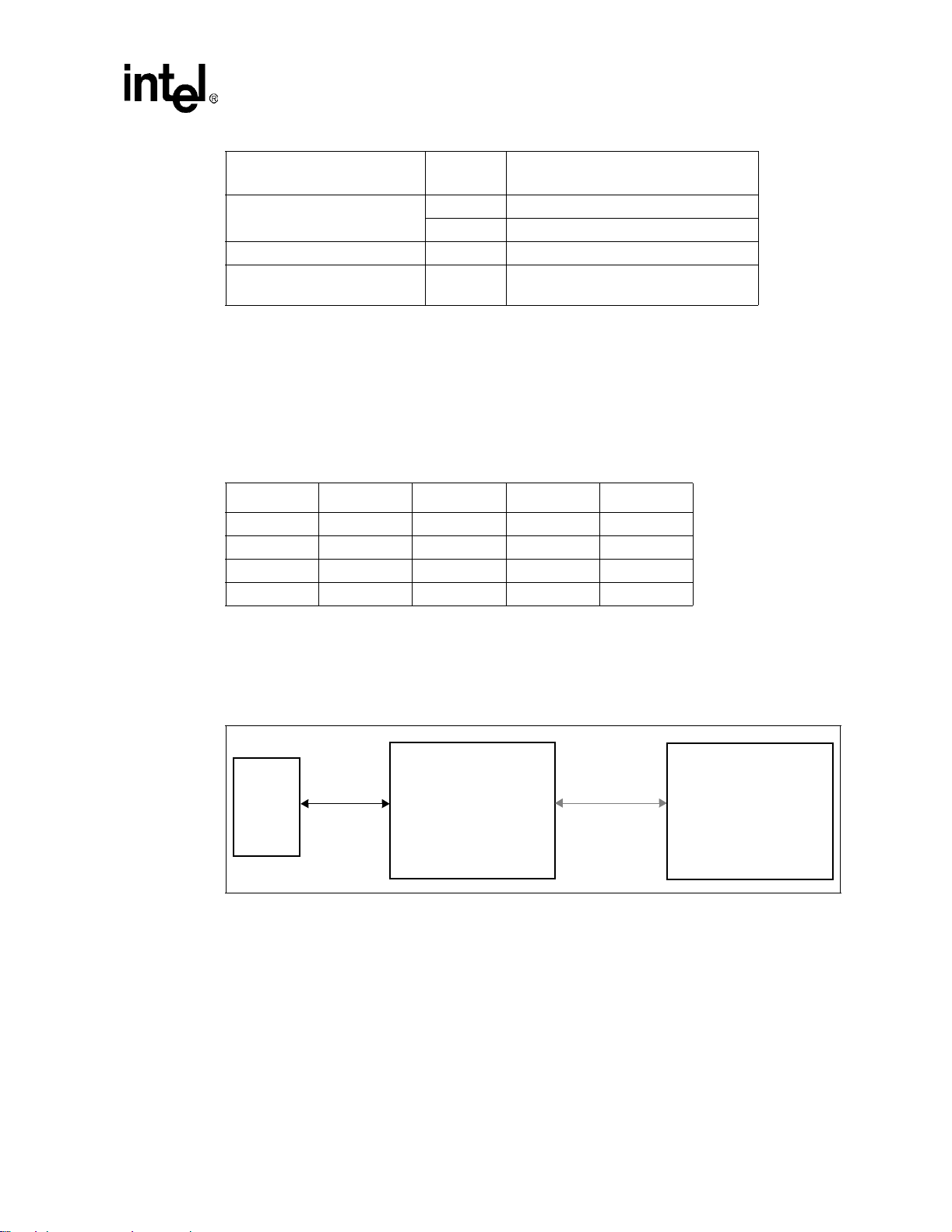
3.9 D iagnostic Testing [S18, &Tn]
The &Tn command initiates loopback tests. Setting S-register S18 to a non-zero value determines
the length of testing after the modem receives the &Tn command. After the te sting period elaps e s,
the modem halts the test and returns to command mod e. To abort the test before the test timer has
timed out, enter the escape code sequence followed by AT&T0. Setting S18 to an ’0’ disables the
test timer . In t his case, the lo opback t est co ntinu es to run unti l an escap e code, f oll owed by AT&T0
(or ATH), is sent to the modem.
The modem provides a local anal og loopback test (see Section 3.9.1, “Local Analog Loopback
[AT&T1]” on page 36) for testing modem-to-modem integrity in a ll modes except V.90 and V.92.
After entering the loopback mode, the com munication integrity is checked by the DTE sending
data to the modem and then checking the looped- back data for errors. In addition, in the self-test
mode the modem implements an internal data pattern generator and checker that detects errors.
When a data error occurs in self-test mode, the modem increments an internal error cou nter. Upon
completing the test, the modem sen ds a three-digit error count to the DTE. These tests are
illustrated in the foll owing examples.
3.9.1 Local Analog Loopback [AT&T1]
This test is u s ed by the local DTE t o check the DTE-to-modem co mmun ication integrity. The local
DTE will not initiate the test from online command mode.
36 536EX Chipset Developer’s Manual
Intel Confidential
Page 37

Figure 6. Loca l Analog Loopback Test
Data Mode AT COMMANDS
LOCAL MODEM
TXD
DTE
RXD
TRANSMITTER
RECEIVER
Local Modem (or Test Modem)
AT&F &W<CR> Returns the modem to the factory defaults.
AT S18 = 0 &T1 Causes the modem to ru n local analog loopback without self-test.
CONNECT 115200 Modem response code indicates that analog loopback is
enabled with a DTE speed of 115200.
This is a test. Test string that the user could type at the keyboard . If the received data
is the same as the test string, then the DTE-to-mod em co mmunication
channel is working properly.
+++AT TIES Escape Sequence is used to return to command mode.
OK Modem enters command mode.
AT&T0 Terminates any loopback test.
OK Modem aborts analog loopback and stays in command mode.
3.9.2 Local Analog Loopback With Self-Test [AT&T8]
This test is used by the local DTE to check the DTE-to-modem communication integrity.
Figure 7. Loca l Analog Loopback with Self-Test
LOCAL MODEM
TXD
DTE
RXD
536EX Chipset Developer’s Manual 37
Intel Confidential
PATTERN
GENERATOR
PATTERN
CHECKER
TRANSMITTER
RECEIVER
Page 38

Data Mode AT COMMANDS
Local Modem (or Test Modem)
AT&F &W<CR> Returns the modem to the factory defaults.
AT S18=20 &T8 Causes the modem to start local analog loopback with s elf-test for 20
OK After starting analog loopback, the modem goes back to command
AT The mode m responds to new commands.
OK
000
OK an error count to the DTE, and enters command mode.
AT S18=0 &T8 Causes the modem to start local analog loopback with self-test, which
OK After starting analog loopback, the modem goes back to command
AT The mode m responds to new commands.
OK
AT&T0 After receiving AT&T0 or ATH, the modem stops analog
000 loopback, sends an error count to the DTE, and enters
OK command mode.
seconds.
mode.
After 20 seconds, the modem stops analog loopback, sends
is only term inated by AT&T0 or ATH.
mode.
3.10 AT Escape Sequences
The 56K family provides the industry-standard Time Independent Escape Sequence (TIES). The
DTE sends the escape sequence to return the modem to command state while in the online data
state (that is, connected to anoth er modem) or in diagnostic mode (&Tn commands ).
Intel also makes the Hayes
statement regarding licensing requirements.
Licensing Requirements for Hayes Escape Sequence
The Intel chipsets are manufactu red wit h TIES as the defa ult settin g. It is Hayes’ posi tio n tha t you
must either have or obtain a valid license from Hayes Microcomputer Products, Inc., of Norcr oss,
Georgia, before producing modem systems that use the Hayes Escape Sequence.
Intel accepts no responsibility and does not indemnify nor in any way provide protection for
paten t or po s si ble pat e nt vi ol a ti ons to its cu st omers or users of it s products.
3.10.1 Time-Independent Escape Sequence
The TIES (Time-Independent Escape Sequence), implemented with +++AT, was developed by a
group of modem manufacturers as an alternative to the Hayes Escape Sequence. TIES was
designed for compatibility with existing communication software written for the Hayes Escape
Sequence.
Escape Sequence available to customers; however, see the followi ng
38 536EX Chipset Developer’s Manual
Intel Confidential
Page 39

Data Mode AT COMMANDS
The DTE implements the es cape sequence by sending the escape character (as defined in S2) three
times, followed by a valid AT command, and then the contents of S3 (typic ally a <CR>). Upon
detecting the t hree co nsecutive escape charact ers, t he modem ch anges to TIES co mmand mod e and
starts an inter nal EPD (Escape Prompt Delay) timer (with the time limit defined by S12). The
modem then looks for one of the followin g conditions to occur:
• No additional data is rec eived and the EPD time r times out: the m odem sends an ‘OK’
message to the DTE and then waits indefinitely for an incoming valid AT command string
from the DTE. Until the modem receives a valid AT command, it monitors any data received
from the DTE and passes on the data to the remote modem (that is, the modem does not ech o
back the received character to the DTE).
— If the subsequent character received by the modem is not an ‘A’ or ‘a’, the modem returns
to data mode and sends a ‘CONNECT’ message back to the DTE.
— If the modem receives an ‘A’ or ‘a’, it stores any additional data recei ved from the DTE in
the modem’s internal command buffer and continues to send the data to the remote
modem. The modem then waits until the DTE sends a <CR>, or up to 39 data characters,
before deciding whether to go to command mode or to return to data mode. Upon
detecting a < CR> or receiving the 39 data character s , the modem determines if a valid AT
command has been received. If a non-AT command string or an invalid co mm a nd string
has been received, then the modem changes back to data mode and sends a ‘CONNECT’
message to the DTE. If a valid AT command has been received, the modem changes to
command mode and sends an ‘OK’ message. After sending the ‘OK’ mess age, the m odem
echoes any received data from the DTE while in command mode.
• An ‘A’ or ‘a’ is received from the DTE. The modem disables the E PD timer and sends the
character to the remote modem. The modem then stor es an y received data from the DTE into
the modem internal command buffer and sends the data to the remote mode m . U pon detecting
a <CR> or receiving up to 39 data characters , th e mode m determines if a valid AT command
has been received; if so, it processes the valid commands. If a non -AT command string or an
invalid command string has been received, then the modem remains in data mode. If a valid
AT command has been received, then the modem changes to command mode and sends an
‘OK’ message. After sending this , the mod em (whi le in command m ode) ech oes back a ny data
received from the DTE.
• Any character except an ‘A’ or ‘a’ is received from the DTE. The modem di sables the EPD
timer and changes back to data mode.
If an AT command string is received while in TIES command mode, the modem processes any
valid AT command. Upon detecting an invalid AT command, the modem cha nges back to data
mode and issues a ‘CONNECT’ message to the DTE. While in TIES command mode, the modem
ignores certain characters that may cause the modem to incorrectly decide that an incoming AT
string is invalid. The ignore charac ters are <LF> , <space>, and <CR> (<CR> is ignored only when
S3 is not equal to <CR>) . Not all AT commands are supported during TIES command mode. The
following is a list of supported commands:
En, Hn, Mn, On, Qn, Sn, Vn, Xn, and ‘&’ commands (except &Tn a nd &F)
The escape character is determined by the value stored in S-register S2, and it is typical ly a ‘
character. The following is an example of the TIES Escape Sequence:
Format:
<char1><char2><char3><AT command><contents of S3>
char1 = ch a r 2 = ch ar3 = esca pe ch a r a ct e r (S 2)
+’
Example:
536EX Chipset Developer’s Manual 39
Intel Confidential
Page 40

Data Mode AT COMMANDS
DTE: +++ AT<CR>
DCE: OK
Note: TIES requires that the three-character escape sequence be contiguous and not repeated. The
character immediately preced ing the first character of the three-character se quence cannot be the
same as the escape character. Therefore, ‘
3.10.2 Hayes* Escape Sequence
In this escape sequence, implemented with +++, the DTE sends the modem an escape character
three times, preceded and follo wed by guard times. Upon detecting the escape sequen ce, the
modem sends an ‘OK’ response to the DTE. To re-enter the online data state, the DTE then sends
the modem ATO followed by the contents of S-register S3 (typically a <CR>).
+++ AT<CR>’ is valid, but ‘++++ AT < CR>’ is not.
The escape character is determined by the value stored in S-register S2 and is typically a ‘
character. Guard times are silence times when the DTE does not send any data to the modem.
Guard times ensure that the modem does not falsely detect an escape sequence if three consecutive
escape characters are recei ved from th e DTE. The preced ing and followin g guard times are defin ed
in S-register S12. T ypicall y , these guard times are 1 second. In addition to the preceding and ending
guard times, there are inter-character time-outs between each escape character sent. The intercharacter time-outs define the maximum amount of time allowed betwe en char acters before the
modem ignores the previous escape characters. This inter-character delay time is set to 1 second.
An example of the Hayes Escape Sequence follows:
Format:
<gt1><char1><tm 2><char2><tm3><char3><gt4>
gt1 = gt4
≥ preceding and following guard times (S12)
tm2 = tm3
≤ inter-character time-out (= 1 second)
char1 = char2 = char3 = escape ch aracter (S2)
Example:
DTE: 1 second +++ 1 second
DCE: OK
Table 18. Data Mode Command Descriptions
Command Default Description
Repeat Last Command: This command re-e xecutes the last AT command string stored in the c ommand
buffer. A/ is the only command not preceded by AT and ended by a carriage return.
A/ none
A none
Cn 1
NOTE: An asterisk (*) denotes the factory-default setting.
Sending any character (such as a carriage return) after A/ and before a modem response is sent to the
DTE causes the modem to abort the remainder of the command string in the modem internal command
buffer.
Answer Command: This command causes the modem to immediately go off-hook and initiate an
answer mode handshake without waiting for an incoming ring signal. This command is useful for
manually answering a call or establishing a back-to-back connection with an originate-mode modem.
Carrier Control Option: This command is reserved for selecting between controlled carrier or constant
carrier modes. This modem supports only constant carrier mode.
n = 0 Transmit carrier always off (returns an ERROR message)
n = 1* Normal transmit carrier (constant carrier)
+’
40 536EX Chipset Developer’s Manual
Intel Confidential
Page 41

Table 18. Data Mode Command Descriptions (Continued)
Command Default Description
Dial Co mm a nd : This co mmand caus es the mo dem to immediately go off-hook as an originating modem
and dial a telephone number with correspo nding dial modifiers. Dial modifiers are p ar ameters tha t define
how the modem should dial the telephone number.
Dial Modifiers
0–9 Dialing Digits
A, B, C, Tone Dial Characters
D, *, #
P Pulse Dial—configures the modem to use pulse dialing to dial a telephone number.
R Reverse Originate Mode—places the modem in answer mode. This modifier should be the
S = n Dial NVRAM Telephone Number—causes the modem to dial a telephone number
D none
En 1
Hn 0
NOTE: An asterisk (*) denotes the factory-default setting.
T Tone Dial—configures the modem to use DTMF tones to dial a telephone number.
W Wait for Dial Tone—causes the modem to look for dial tone for a specified amount of time.
, Pause—causes the modem to pause or delay implementing the next parameter in the dial
!Flash Hook—causes the modem to go on-hook for 0.75 seconds.
@ Wait for Quiet Answer—causes the modem to wait for specified amount of time (S-register
; Return to Idle State—causes the modem to enter online command mode without initiating a
<space> - ( ) Ignored by Modem—these four characters ar e ign ored by the modem. Spaces als o may be
Command Mode Echo: This command selects whether the modem echoes AT commands back to the
host in either online or off-line command mode.
n = 0 Echo disabled
n = 1* Echo enabled
Switch Hook Control: This command controls the telephone line relay (OHREL*) and causes the
modem to either hang up or pick up the telephone line.
n = 0* Hang up telephone line (go on-hook)
n = 1 Pick up telephone line (go off-hook)
last character in the dialing string (for example, ATDT 12345678R). After dialing the
telephone number, the modem goes into data modem answer mode instead of originate
mode.
previously stored in the NVRAM with the AT&Zn=x command.
If dial tone or the amount of time specified by the S-register, S6, times out, the modem
processes the next command in the dial string. If a busy signal is detected, the modem
responds to the DTE with a busy response code and then goes into off-line command
mode.
string by the time specified in S-register S8.
S7) followed by 5 seconds of silence before processing the next dial modifier.
data modem handshake (used for phone directory auto-dialers).
included in the dial string to separate area codes and numbers.
Data Mode AT COMMANDS
536EX Chipset Developer’s Manual 41
Intel Confidential
Page 42

Data Mode AT COMMANDS
Table 18. Data Mode Command Descriptions (Continued)
Command Default Description
Identification/Checksum Option: This command causes the modem to send product code and
hardware setup information to the DTE.
n = 0* ROM Checksum
n = 1 Modem name
n = 2 Manufacturer
n = 3 Chipset
n = 4 Firmware version
In 0
Ln 2
Mn 1
On 0
P none
Qn 0
Sn none
Sn=x none
Sn? none
NOTE: An asterisk (*) denotes the factory-default setting.
n = 5 Modem chip hardware configuration
n = 6 DSP patch level
n = 12 Country code
n = 7–11, Reserved
13, 14,
20–25
Example:
ATI2
Intel Corporation
OK
Speaker Volume Control: This command selects the modem’s speaker volume.
n = 0 Low speaker volume
n = 1* Low speaker volume
n = 2 Medium speaker volume
n = 3 High speaker volume
Speaker Control: This command specifies when the speaker is turned on and off.
n = 0 Speaker always off
n = 1* Speaker on until carrier present
n = 2 Speaker always on
n = 3 Speaker off during dialing, and on until carrier
Go Online: This command causes the modem to return back to online data mode from online command
mode.
n = 0* Returns the modem to data mode
n = 1 Begins an equalizer retrain sequence; then returns to data mode
n = 3 Renegotiates rate and then returns to data mode
Select Pulse Dialing: This command configures the modem to use pulse dialing next time the modem
dials a telephone number.
Result Code Display Control: This command selects whether the modem sends result codes to the
DTE.
n = 0* Result codes enabled
n = 1 Result codes disabled
Select an S-Register: This command selects the current S-register.
n = 0–33
Write to an S-Register: This command writes a decimal number ‘x’ to S-register ‘n’.
n = 0–33
x = 0–255
Read an S-Register: This command is used to read a decimal number from S-register ‘n’.
n = 0–33
42 536EX Chipset Developer’s Manual
Intel Confidential
Page 43

Table 18. Data Mode Command Descriptions (Continued)
Command Default Description
Data Mode AT COMMANDS
T none
Vn 1
Wn 0
Xn 4
NOTE: An asterisk (*) denotes the factory-default setting.
Select Tone Dialing: This command configures the modem to use DTMF tones the next time the
modem dials a telephone number (touch tone dialing).
Result Code Form: This command selects whether the modem’s basic syntax response codes are in
numeric or verbose form.
n = 0 Numeric form
n = 1* Text form
Response Code Data Rate: This command selects whether the modem sends the DTE independent
modem connection extended syntax result codes for modulation mode, speed, error control protocol, or
data compression before the final 'CONNECT' message. This command does the selection by enabling
and disabling the appropriate V.250 reporting commands (+MR, +ER, +DR, and +ILRR).
n = 0*, 1 CONNECT result code reports DTE speed.
For example:
+ILRR: 115200
CONNECT 50666
n = 2 CONNECT result code reports modulation mode and DCE transmitter speed.
For example:
+MCR: V90
+MRR: 28800
CONNECT 50666
n = 3 CONNECT result code reports DTE data rate, modulation mode, error correction, data
compression, DCE transmitter speed and DCE receiver speed.
For example:
+MCR: V90
+MRR: 28800
+ER: LAPM
+DR: V42B
+ILRR: 115200
CONNECT 50666
n = 4 CONNECT result code reports modulation mode, error correction, data compres sion, DCE
transmitter speed and DCE receiver speed.
For example:
+MCR: V90
+MRR: 28800
+ER: LAPM
+DR: V42B
CONNECT 50666
Please refer to +MR=m, +ER=m, +DR=m and +ILRR=m for a detailed description of each
command.
Result Code Type/Call Progress: This command determines which modem result codes are enabled.
Additionally, this command specifies whether busy and dial tone detection are enabled or disabled.
n = 0 Result codes 0–4 enabled. Busy and dial tone detect disabled.
n = 1 Result codes 0–5, 10 and above enabled. Busy and dial tone detect disabled.
n = 2 Result codes 0–6, 10 and above enabled. Busy detect disabled and dial tone detect
enabled.
n = 3 Result codes 0–5, 7, 10 and above enabled. Busy detect enabled and dial tone detect
disabled.
n = 4* Result codes 0–7, 10 and above enabled. Busy and dial tone detect enabled.
536EX Chipset Developer’s Manual 43
Intel Confidential
Page 44

Data Mode AT COMMANDS
Table 18. Data Mode Command Descriptions (Continued)
Command Default Description
Long Space Disconnect: This command determines whether the modem disconnects after receiving
1.6 seconds of silence and whether the modem sends a period of silence to the remote modem before
disconnecting.
Yn 0
Zn 0
&Cn 1
&Dn 2
&F none
&Gn 0
&Kn 3
NOTE: An asterisk (*) denotes the factory-default setting.
n = 0* Disables long space disconnect
n = 1 Enables long space disconnect. The modem disconnects after receiving 1.6 seconds of
silence from the remote modem. Additionally, after receiving an ATH0 command, the
modem sends at least 4 seconds of silence before hanging up.
Reset Modem/Recall Stored Profile: This command causes the modem to go on-hook (hang-up),
perform a warm reset, and load user-configuration profile ‘n’ (previously stored in the NVRAM) into the
active profile. The Zn command must be the last command in command string, as it causes all
subsequent commands to be ignored.
n = 0* Resets the modem and recalls user profile 0
n = 1 Resets the modem and recalls user profile 1
DCD (Data Carrier De tect) Option: This command controls how the modem functions in relation to the
DCD or RLSD signal.
n = 0 State of carrier from remote modem is ignored. DCD is always on.
n = 1* State of carrier from remote modem is tracked. DCD reflects the state of the received
carrier.
DTR (Data Terminal Ready) Option: This command controls how the modem responds to DTR. After
toggling DTR, the host should wait 200 ms before modifying the UART registers or sending a new
command to the modem. This is done becaus e the mo dem does not send an ‘OK’ message to indicate it
has performed the requested function.
n = 0 In asynchronous mode (&Q0), the modem ignores DTR.
n = 1 The modem switches from data mode to command mode when an on-to-off transition of
DTR occurs.
n = 2* An on-to-off transition of DTR causes the modem to go on-hook (hang up). While DTR is
off, auto-answer is disabled.
n = 3 An on-to-off transition of DTR re-initializes the modem. The re-initialize procedure performs
the same function as a power-up reset, except that the UART registers are not
reconfigured.
Load Factory Defaults: This command loads command defaults and S-register factory defaults into the
active configuration and configures the modem for data mode.
Guard Tone Option: This command controls whether the modem sends out guard tones while
connected to a remote modem (for ITU-T V.22 bis [1200 bps] and V.22 bis [2400 bps] connections only).
Guard tones may be required in some countries but are not needed in the United S tates. Guard tones are
sent by the answer modem to disable Central Office echo cancelers.
n = 0* Guard tone disabled
n = 1 550 Hz guard tone enabled
n = 2 1800 Hz guard tone enabled
Select Serial Port Flow Control: This command specifies the DTE-to-modem flow control. Software
flow control uses the characters XOFF (13h) and XON (11h) to stop and start data transmission,
respectively, both to and from the DTE. Bidirectional hardware flow control uses RTS/CTS to stop and
start data from the modem.
n = 0 Disables flow control
n = 3* Bidirectional hardware flow control—RTS/CTS
n = 4 XON/XOFF software flow control
44 536EX Chipset Developer’s Manual
Intel Confidential
Page 45

Table 18. Data Mode Command Descriptions (Continued)
Command Default Description
Dial Pulse Ratio: This command determines the make/break (that is, off-hook/on-hook) ratio during
pulse dialing.
&Pn 0
&Sn 0
&Tn 0
&Un 0
n = 0* Make = 39%; Break = 61% at 10 pulses per second—for use in the United States.
n = 1 Make = 33%; Break = 67% at 10 pulses per second—for use in the United Kingdom and
Hong Kong.
DSR (Data Set Ready) Option: This command controls how the modem treats the DSR signal.
n = 0* DSR circuit always on
n = 1 DSR circuit is on during handshaking, off in test or idle modes. DSR is off when the carrier
is lost.
Data Mode Self-T est C ommand: This comman d is used in data mode ( except x2 and V.90 connections)
to initiate and terminate loopback tests for testing modem-to-modem and DTE-to-modem data
communication integrity.
n = 0* Terminates test in progress
n = 1 Local analog loopback
n = 8 Local analog loopback with self-test
Disable Trellis Coding: This command selects whether the modem transmits or receives modulated
9600 bps carrier with QAM or Trellis encoding for V.32.
n = 0* Enabled (Trellis modulation with QAM modulation as a fallback)
n = 1 Disabled (QAM modulation only)
View Active Configuration and Stored Profiles: This command causes the modem to display the
command and S-register information contained in the active user profile and in one of two stored
profiles.The command &V0 displays the active profile and the stored profile 0; &V1 displays the active
profile and the store d profil e1. The infor mation in the active profile is stor ed into the us er pr ofile s with the
&Wn command. &W0 stores the active profile into the stored profile 0; &W1, the stored profile 1.
n = 0* Stored profile 0
n = 1 Stored profile 1
Data Mode AT COMMANDS
AT&V0
ACTIVE PROFILE:
E1 L2 M1 T Q0 V1 W0 X4 Y0 &C1 &D2 &G0 &J0 &K3 &P0 &S0 &Y0
%A013 %C1 %E1 \A3 \C0 \G0 \J0 \T000 \X0 -J1
&Vn 0
NOTE: An asterisk (*) denotes the factory-default setting.
S00:000 S01:000 S02:043 S03:013 S04:010 S05:008 S06:002 S07:060 S08:002
S09:006 S10:014 S11:070 S12:050 S18:000 S25:005 S27:064 S32:032 S33:010
+ES=003,000,002 +DS=003,000
STORED PROFILE 0:
E1 L2 M1 T Q0 V1 W0 X4 Y0 &C1 &D2 &G0 &J0 &K3 &P0 &S0
%A013 %C1 %E1 \A3 \C0 \G0 \J0 \T000 \X0 -J1
S00:000 S02:043 S06:002 S07:060 S08:002 S09:006 S10:014 S11:070 S12:050
S14:138 S18:000 S21:048 S22:118 S23:048 S25:005 S27:064 S30:000 S32:032
S33:010 +ES=003,000,002 +DS=003,000
TELEPHONE NUMBERS:
&Z0 = &Z1 =
&Z2 = &Z3 =
536EX Chipset Developer’s Manual 45
Intel Confidential
Page 46

Data Mode AT COMMANDS
Table 18. Data Mode Command Descriptions (Continued)
Command Default Description
Store Active Profile: This command caus es the modem to stor e a subset of the active profi le comma nd
&Wn 0
&Yn 0
&Zn=x none
%En 1
%Gn 1
-Cn 0
NOTE: An asterisk (*) denotes the factory-default setting.
and S-register configurations into the NVRAM user profile ‘n’.
n = 0* Store in user profile 0
n = 1 Store in user profile 1
Select Stored Profile on Power-up: This command selects the particular stored user profile from the
NVRAM to be loaded into the active profile upon modem power-up.
n = 0* Select profile 0
n = 1 Select profile 1
Store Telephone Number: This command stores a telephone number up to 30digits (including dial
modifiers) in the NVRAM. To dial the stored telephone number, use the ATDS=m command. Use the &V
command to see the stored telephone number.
n = 0–3
x = 0–9 A B C D # * T P R W @ , ! ;
Auto-Retrain Control: This command controls whether the modem automatically initiates a modem
retrain whenever the received data signal quality falls below a threshold that may affect data reliability.
The value for ‘n’ is stored in the NVRAM.
n = 0 Disabled
n = 1* Enabled
Rate Renegotiation: This command selects whether the modem automatically initiates a change to a
higher speed or lower speed depending on received signal qual ity ( that is, rate negotia tion) . The modem
always responds to any rate change initiated by the remote modem.
n = 0 Disabled
n = 1* Enabled
Generate Data Modem Calling Tone: This command allows the DTE to select whether the modem
sends a 1300 Hz calling tone or V.8 calling tone when originating a data modem connection.
n = 0* Calling tone disabled
n = 1 1300 Hz calling tone sent for all data modem connections
n = 2 V.8 calling tone sent for V.34 modulation and 1300 Hz calling tone sent for all other
modulations
46 536EX Chipset Developer’s Manual
Intel Confidential
Page 47

Table 18. Data Mode Command Descriptions (Continued)
Command Default Description
V.8 and V.8 bis Operation Controls: This command configures V.8 and V.8 bis operation. If issued
when the DCE is on-hook, this command is a compound parameter used to precondition V.8 and V.8 bis
originating and answering operation. It is not supported as an actio n command while the DCE is off-hook.
If enabled, V.8 negotiation does not preclude simultaneo us im plement ation of other m eans of negotiati on
(for example, V.8 bis, V.18, and V.32 bis Annex A).
For the +A8E default values, the signal indicators are not generated by the DCE. When the parameters
<v8o>=6 and <v8a>=5, the +A8I, +A8C, +A8A, +A8J, and +A8M indications are sent from the DTE, but
the +A8M command is not used because the DCE controls the V.8 section.
m = <v8o>, <v8a>, <v8cf>, <v8b>,<cfrange>, <protrange>
Defaults: 1, 1, C1, 0, ,
<v8o> V.8 origination selection.
Range: 0, 1, 6
0 Disable V.8 origination negotiation
1* DCE-controlled V.8 origination negotiation
6 DCE-controlled V.8 origination negotiation, enable indications only
<v8a> V.8 answer selection.
Range: 0, 1, 5
0 Disable V.8 answer negotiation
1* DCE-controlled V.8 answer negotiation
5 DCE-controlled V.8 answer negotiation, enable indications only
+A8E=m see ‘m’
NOTE: An asterisk (*) denotes the factory-default setting.
<v8cf> V.8 call function
Range: 0x21, 0xC1
0x21 Sets the V.8 call function to indicate H.324.
0xC1* Sets the V.8 call function to indicate standard data mode.
<v8b> V.8 bis control
Range: 0
0* Disable V.8 bis negotiation
<cfrange> Not supported.
<protrange> Not supported.
Indication Definition
+A8A:1
+A8A:2
+A8I:<v8cf>
+A8M:<CM>
+A8M:<JM>
+A8J:[0,1]
Indicates V.8 ANSam has been detected. This indication is only sent to the DTE if
+A8E<v8o>=6 and operating in originate mode.
Indicates V.25 answer tone (2100 Hz) has been detected. This indication is only sent to
the DTE if +A8E<v8o>=6 and operating in originate mode.
Indicates the detection of a V.8 CI-signal and the recovered call function (only if
+A8E<v8a>=5 and operating in answer mode).
Indicates the hexadecimal-coded CM signal (only if +A8E<v8a>=5 and operating in
answer mode)
Indicates the hexadecimal-coded JM signal (only if +A8E<v8o>=6 and operating in
originate mode)
Indicates the modem is transmitting the V.8 termination signal. +A8J:1 indicates
transmission or detection of CJ while +A8J:0 indicates time-out while waiting for a CJ
signal.
Data Mode AT COMMANDS
536EX Chipset Developer’s Manual 47
Intel Confidential
Page 48

Data Mode AT COMMANDS
Table 18. Data Mode Command Descriptions (Continued)
Command Default Description
Break Handling: Controls break handling in error control operation. It accepts three numeric
subparameters:
Syntax:
+EB = <break selection>, <timed>, <default length>
<break selection> specifies the type of break to be signaled to the remote DCE upon detecting one from
the local DTE.
0 Ignore Break (do not signal to remote DCE)
1 Non-expedited, non-destructive
2 Expedited, non-destructive
+EB 1, 0, 30
NOTE: An asterisk (*) denotes the factory-default setting.
3 Expedited and destructive
<timed> specifies if the break signal to be signaled to the remote DCE is timed or not.
0 Sent without a break signal length
1 Sent with break signal length
<default length> specifies the amount of time in tens of milliseconds that a break should be signaled to
the local DTE when an indication of a break is received from the remote DCE without explicitly indicated.
0 D o not deliver received break to DTE
1 Default break length 0.01 to 2.54 seconds. Used for default to signal DTE when break
received from the remote DCE without break length
Controls the use of breaks in V.42.
48 536EX Chipset Developer’s Manual
Intel Confidential
Page 49

Table 18. Data Mode Command Descriptions (Continued)
Command Default Description
Synchronous Access Mode Configuration: controls the manner of operation of the Synchronous Access
Mode in the DCE (if present).
Syntax:
+ESA=[<trans_idle>[,<framed_idle>[,<framed_un_ov>[,<hd_auto>[,<crc_type>[,<nrzi_en>[,<syn1>[,<sy
n2>]]]]]]]]
<trans_idle> specifies the bit sequence transmitted by the DCE when a transmit data buffer underrun
condition occurs, while operating in Transparent sub-Mode.
0 In Transparent sub-Mode, DCE transmits 8-bit SYN sequence on idle. DCE receiver does
1 In Transparent sub-Mode, DCE transmits 8-bit SYN sequence on idle. DCE receiver hunts
2 In T ranspar ent sub-Mode, DCE tran smits 16-bit SYN sequen ce on idle. DCE receiv er hunts
<framed_idle> specifies the bit sequence transmitted by the DCE when a transmit data buffer underrun
condition occurs immediately after a flag, while operating in Framed sub-Mode.
0 In Framed sub-Mode, DCE transmits HDLC flags on idle
1 In Framed sub-Mode, DCE transmits marks (ones) on idle
<framed_un_ov> specifies the actions undertaken by the DCE when a transmit data buffer underrun or
overrun condition occurs immediately after a non-flag octet, while operating in Framed sub?Mode.
0 In Framed sub-Mode, DCE transmits abort on underrun in middle of frame
1 In Framed sub-Mode, DCE transmits a flag on underrun in middle of frame, and notifies
<hd_auto> specifies whether or not, in V.34 half duplex operation, additional procedures besides those
0, 0, 1,
, 0, 0,
NOTE: An asterisk (*) denotes the factory-default setting.
specified in clause 12/V.34 shall be performed by the DCE when switching from primary channel to
secondary channel operation, and vice versa.
0,
0 When s witching betw een pri mary and s econdar y channel operation in V .34 ha lf duplex , the
1 When s witching betw een pri mary and s econdar y channel operation in V .34 ha lf duplex , the
<crc_type> specifies the CRC polynomial used while operating in Framed sub-Mode.
0 CRC generation and checking disabled
1 In Framed sub-Mode, the 16-bit CRC specified in 8.1.1.6/V.42 is generated by the DCE in
2 In Framed sub-Mode, the 32-bit CRC specified in 8.1.1.6/V.42 is generated by the DCE in
<nrzi_en> specifies if N on Return to Zero Inverted (NRZI) encodi ng is to be used by the DCE for transm it
and receive data.
0 NRZI encoding and decoding disabled
1 NRZI encodi ng enabl ed i n the DCE in the transmit dir ect ion, a nd N RZI decodi ng enabled in
<syn2> specifies the octet value(s) to be used while performing character-oriented framing.
0–255 When <trans_idle>=0, specifies the 8-bit transmit idle sequence to be used by the DCE.
<syn1> specifies the octet value(s) to be used while performing character-oriented framing.
0–255 When <trans_idle>=2, specifies last 8 bits of 16-bit synchronization sequence to be used
not hunt for synchronization sequence
for 8-bit SYN sequence
for 16-bit SYN sequence
DTE of underrun or overrun
DCE only executes those procedures defined in clause 12/V.34
DCE executes additional procedures as des cr ibed in 8.8.5 besi des those defin ed in clause
12/V.34
the transmit direction, and checked by the DCE in the receive direction
the transmit direction, and checked by the DCE in the receive direction
the DCE in the receive direction
When <trans_idle>=1, specifies the 8-bit synchron ization sequence to be use d by the DCE.
When <trans_idle>=2, specifies first 8 bits of 16-bit synchronization sequence to be used
by the DCE
by the DCE
Data Mode AT COMMANDS
536EX Chipset Developer’s Manual 49
Intel Confidential
Page 50

Data Mode AT COMMANDS
Table 18. Data Mode Command Descriptions (Continued)
Command Default Description
Selective Repeat: Controls the use of selective repeat (SREJ) option in V.42.
+ESR 1
+ETBM 1, 1, 20
+GCAP none
+GCI=m see ‘m’
+GMI none
+GMM none
NOTE: An asterisk (*) denotes the factory-default setting.
0 D o not use SREJ
1 Use SREJ if available in remote DCE; continue without it if not
2 Use SREJ if available in remote DCE; disconnect if SREJ is not available
Call Termination Buffer Management: Controls the handling of data remaining in the DCE buffers upon
call termination. It accepts three numeric parameters:
Syntax:
+ETBM = <pending TD>, <pending RD>, <timer>
<pending TD> controls how previously transmitted data r emai ning in the DCE buffers shoul d be handled
when the local DTE requests disconnection of the call.
0 D iscard all buffered data immediately and disconnect
1 Attempt until all data is delivered and acknowledged (ignoring timer); if remote DCE
disconnects discard remaining data
2 Attempt until all data is delivered and acknowledged; if timer expires or remote DCE
disconnects, discard remaining data
<pending RD> controls how previously received data remaining in the DCE buffers should be handled
when the remote DCE disconnects the call.
0 D iscard all buffered data immediately and disconnect
1 Attempt until all data is delivered (ignoring timer); if local DTE requests disconnect discard
remaining data
2 Attempt until all data is delivered; if timer expires or local DTE requests disconnect discard
remaining data
<timer> sets a maximum time limit that the DCE will attempt to deliver the buffered data before
disconnecting and discarding the remaining
0–30 Delivery timer value in seconds
Request Complete Capabilities List: This extended-for mat command causes the DCE to trans mit a list
of additional capabilities commands.
AT+GCAP
+GCAP: +FCLASS,+MS,+ES,+DS
OK
Identify Country of Installation: This extended command is used to indicate and select the country of
installation for the DCE. The DTE may use this value to determine country-specific functions. To
determine what countries the DCE supports, issue the AT+GCI=? command. Refer to the ITU-T T.35
recommendation for the details on what country code is used for each country.
Default: country of installation
m = country code, e.g., United States
AT+GCI=B5
Identify Modem Manufacturer: This command causes the DCE to send a message to the DTE
indicating the DCE manufacturer. This command is identical to AT+FMFR? and AT+FMI.
AT+GMI
Intel Corporation
OK
Identify Product Model: This command causes the DCE to report the modem chipset name. This
command is identical to AT+FMDL? and AT+FMM commands.
AT+GMM
Intel 536EP V.92 Modem
OK
50 536EX Chipset Developer’s Manual
Intel Confidential
Page 51

Table 18. Data Mode Command Descriptions (Continued)
Command Default Description
Identify Product Revision: This command causes the DCE to report the modem chipset revision level.
This command is identical to AT+FREV? and AT+FMR. The response message depends on the
+GMR none
+GSN none
+IFC 2, 2
+ILRR=m 0
NOTE: An asterisk (*) denotes the factory-default setting.
firmware version.
AT+GMR
536EP Release 4.28 - Dec 10 2001
OK
Request Product Serial Number Identification: This command causes the DCE to transmit a message
to the DTE indicating the product serial number identification.
Syntax:
AT+GSN
+GSN: PCI\VEN_8086&DEV_1040&SUBSYS_00000000&REV_00
OK
The modem responds with the hardware Id key from the registry that contains the VendorID, SubVendor
Id, Subsystem VendorId, Device ID, and hardware revision.
DTE-DCE Local Flow Control: Controls the flow control between local DTE and DCE when V.42 error
control or normal mode (buffering mode or speed matching) is being used. In addition to acting locally
the flow control characters can be passed on to remote DCE to act upon. It accepts two numeric
subparameters:
<DCE_by_DTE> specifies the method to be used by the DTE to control the flow of received data from
the DCE; and
<DTE_by_DCE> specifies the method to be used by the DCE to control the fl ow of trans mitted dat a from
the DTE.
<DCE_by_DTE>
0 none
1 DC1/DC3 software flow control; do not pass DC1/DC3 characters to the remote DCE
2 RTS/CTS—hardware flow control
3 DC1/DC3 softw are flow control wit h DC1/DC3 characters bei ng pas sed to the remote DCE
in addition to being acted upon for local flow control
<DTE_by_DCE>
0 None
1 DCI/DC3 software flow control
2 RTS/CTS hardware flow control
DTE to DCE Local Rate Reporting: Controls whether the “+ILRR:” result code is transmitted from the
DCE to the DTE once a connection has been made. If enabled the result code displayed shall represent
the current negotiated DTE-DCE rate, and is issued after any Modulation (+MR :), Error C ontrol ( +ER:) or
Data Compression (+DR:) reports and before the final result code “CONNECT”. +ILRR accepts one
numeric parameter decimal value and the format is as follows:
0 Disables reporting of local port rate (no +ILRR intermediate result code transmitted)
1 Enables reporting of local port rate (+ILRR intermediate result code transmitted)
Example response message when +ILRR = 1,
+ILRR: 19200
Data Mode AT COMMANDS
536EX Chipset Developer’s Manual 51
Intel Confidential
Page 52

Data Mode AT COMMANDS
Table 18. Data Mode Command Descriptions (Continued)
Command Default Description
Modulation Automode Control: This command specifies the alternative to the preferred modulation
specified in the +MS=<carrier> command. Alternative modulations are only available when
+MS=,<automode> enables automode. The alternative modula tions av ailable for the +MA command are
limited to all modulations the modem supports below the preferred modulation specified by
+MS=<carrier>. The +MA parameters are reset to all modulations supported by the modem below the
preferred modulation whenever the +MS=<carrier> changes the preferred modulation. The order of
priority of alternative modulations is determined by such mechanisms as V.8 and PN2330, not the order
in which they were entered for this command. <carrier> values omitted are no available as alternative
modulations.
m= <carrier>,<carrier>,…<carrier>
+MA=m none
+MR=m 0
NOTE: An asterisk (*) denotes the factory-default setting.
Defaults: all modulations below +MS=<carrier> and allowed by the DCE limits in the +MS command
<carrier> specifies the al ternative modulati ons that ar e av ailabl e. A tabl e of these mo dulations ar e give n
in +MS command description.
+MA? will display a list of enabled alternative modulations
+MA=? will di splay a list of available alternati ve m odulatio ns. This list is determined by the curr ent val ues
of the +MS parameters for preferred modulation, automode and DTE rate limits. For example:
If +MS=<V32B>, V.34, V.90, and V.92 will not be available because they are above V.32 bis.
If +MS = ,0,, no alternative modulations will be available.
If +MS=V34,1,4800,33600, V.22 bis will not be available because its maximum DCE bit rate is
2400bps.
Modulation Reporting Control: Controls whether the “+MCR: and +MRR” result codes are transmitted
from the DCE to the DTE once a connection has been made. If enabled the result code displayed shall
represent the current negotiated DCE-DCE modulation and r ate, and are issued befo re the Error Control
(+ER:) or Data Compression reports (+DR:) and before the final result code “CONNECT”. The format is
as follows:
0 Disables reporting of modulation (no +MCR and +MRR intermediate result code
transmitted)
1 Enables reporting of modulation (+MCR and +MRR intermediate result code transmitted)
Example if +MR = 1
+MCR: V34
+MRR: 33600
52 536EX Chipset Developer’s Manual
Intel Confidential
Page 53

Table 18. Data Mode Command Descriptions (Continued)
Command Default Description
Modulation Selection: This command sets the preferred modulation, whether alternative modulations
can be tried, and the transmit and receive DCE bit rates.
m = <carrier>,<automode>,<min rate>,<max rate>,<min rx rate>, <max rx rate>
Defaults: m = V92,1,0,0,0,0
+MS? will display the current +MS parameter settings
+MS=? will display the +MS parameter settings supported by the modem
<carrier> specifies the preferred modulation. The following table contains the modulations supported.
<carrier> Description
BELL103 Bell 103 300bps (FSK)
BELL212 Bell 212A (DPSK)
V21 V.21 300bps (FSK)
V22 V.22 1200bps (QAM)
V22B V.22 bis 1200 or 2400bps (QAM)
V23C V.23 1200bps forward and 75bsp reverse channel (FSK)
V32 V.32 4800 or 9600bps (QAM) or 9600bps (TCM)
V32B V.32 bis 4800 or 9600bps (QAM) or7200, 9600, 12000 or 14400bsp (TCM)
V34 V.34 2400, 4800, 7200, 9600, 12000, 14400, 16800, 19200, 21600, 24000, 26400, 28800,
V90 V.90 4800, 7200, 9600, 12000, 14400, 16800, 19200, 21600, 24000, 26400, 28800, 31200
V92 V.92 24000, 25333, 26666, 28000, 29333, 30666, 32000, 33333, 34666, 36000, 37333,
+MS=m see ‘m’
<automode> enables or disable automatic modulation negotiation. Automatic modulation negotiation
allows the modem to connect with an alternative modulation to the preferred modulation. Alternative to
the preferred modulations are specified by the +MA command. The +MA parameters are reset to all
modulations supported by the modem below the preferred modulation whenever the +MS=<carrier>
changes the preferred modulation.
Range: 0, 1
Default: 1
<automode> = 0 Disable automatic modulation negotiation
<automode> = 1 Enable automatic modulation negotiation
<min rate> and <min rx rate> specifies the lowest bit rate, in decimal units of bits/s, that may be
established on the DCE. If 0, they are determined by the modulation selected by <carrier>, <automode>
and the +MA command. These values are reset to 0 whenever +MS=<carrier> changes the preferred
modulation. <min rx rate> is only used for modulations that support unequal minimum bit rate limits for
the transmit and receive channel like V.23 and V.90 and is used to specify limits for the receive channel
as distinct from the transmit channel.
Range: 0 and the DCE bps given in the <carrier> description table above
Default: 0
<max rate> and <max rx rate> specifies the highest bit rate, in decimal units of bits/s, that may be
established on the DCE. If 0, they ar e determi ned by the modulati on selec ted by <c ar rier>. These val ues
are reset to 0 whenever the +MS=<carrier> changes the preferred modulation. <max rx rate> is only
used for modulations that support unequal maximum bit rate limits for the transmit and receive channel
like V.23 and V.90 and is used to specify limits for the receive channel as distinct from the transmit
channel.
Range: 0 and the DCE bps given in the <carrier> description table above
Default: 0
NOTE: An asterisk (*) denotes the factory-default setting.
31200 or 33600bps
or 33600 bps on the transmit channel and 28000, 29333, 30666, 32000, 33333, 34666,
36000, 37333, 38666, 40000, 41333, 42666, 44000, 45333, 46666, 48000, 49333, 50666,
52000, 53333, 54666 or 56000 bps (PCM) on the receive channel
38666, 40000, 41333, 42666, 44000, 45333, 46666 and 48000 bps on the transmit channel
and 28000, 29333, 30667, 32000, 33333, 34667, 36000, 37333, 38667, 40000, 41333,
42667, 44000, 45333, 46667, 48000, 49333, 50667,52000, 53333, 54667 or 56000 bps
(PCM) on the receive channel
Data Mode AT COMMANDS
536EX Chipset Developer’s Manual 53
Intel Confidential
Page 54

Data Mode AT COMMANDS
Table 18. Data Mode Command Descriptions (Continued)
Command Default Description
Call Waiting Enable: This command controls the action to be taken upon detection of call waiting in a
V.92 DCE.
+PCW=m 0
+PHSW=
m
+PIG=m 1
+PMH=m 0
+PMHF none
+PMHR none
NOTE: An asterisk (*) denotes the factory-default setting.
none
0 Toggle V.24 Circuit 125 and collect Caller ID if enabled by +VCID
1 H ang up
2 Ignore V.92 call waiting
This command causes the DCE to activate/de-activate the hook relay for supporting the 2C relay.
0 connects the telco terminals to the modem
1 connects the telco terminals to the phone terminals
PCM Upstream Ignore: This command controls the use of PCM upstream in a V.92 DCE.
0 Enable PCM upstream
1 Disable PCM upstream
Modem on Hold Enable: This command controls whether or not modem on hold procedures are
enabled during V.92 operation.
0 Enables V.92 modem on hold
1 D isables V.92 modem on hold
V.92 Modem on Hold Hook Flash: This command causes the DCE to go on-hook for a specified period
of time, and then return on-hook. The specified period of time is normally one-half second, but may be
governed by national regulations. If this command is initiated and the modem is not On Hold, ERROR is
returned. This command applies only to V.92 Modem on Hold.
Initiate Modem on Hold: This command requests the DCE to initiate or to confirm a modem on hold
procedure. The DCE shall return ERROR if Modem on Hold is not enabled or if the DCE is in an idle
condition. The DCE shall return the string response +PMHR: <value> where <value> is a decimal value
corresponding to the Modem on Hold timer value received or the request status during the DCE’s
modem on hold exchange procedure as defined below. This response may be delayed depending upon
the context under which the +PMHR command is made, i.e., if the +PMHR is in respons e to an incomi ng
Modem on Hold or if it is initiating a request.
<value> Description
0 V.92 Modem on Hold Request Denied or not available
1 MOH with 10 second time-out Granted
2 MOH with 20 second time-out Granted
3 MOH with 30 second time-out Granted
4 MOH with 40 second time-out Granted
5 MOH with 1 minute time-out Granted
6 MOH with 2 minute time-out Granted
7 MOH with 3 minute time-out Granted
8 MOH with 4 minute time-out Granted
9 MOH with 6 minute time-out Granted
10 MOH with 8 minute time-out Granted
11 MOH w i th 12 minute time-out Granted
12 MOH wi th 16 minute time-out Granted
13 MOH with indefinite time-out Granted
54 536EX Chipset Developer’s Manual
Intel Confidential
Page 55

Table 18. Data Mode Command Descriptions (Continued)
Command Default Description
Modem on Hold Timer: This command controls whether or not the modem will grant or deny a Modem
on-hold (MOH) request as well as setting the Modem-on-Hold-Time-Out.
0 Deny V.92 Modem-on-hold Request
1 Grant MOH with 10 second time-out
2 Grant MOH with 20 second time-out
3 Grant MOH with 30 second time-out
4 Grant MOH with 40 second time-out
+PMHT=m 0
+PQC=m 0
+PSS=m 2
NOTE: An asterisk (*) denotes the factory-default setting.
5 Grant MOH with 1 minute time-out
6 Grant MOH with 2 minute time-out
7 Grant MOH with 3 minute time-out
8 Grant MOH with 4 minute time-out
9 Grant MOH with 6 minute time-out
10 Grant MOH with 8 minute time-out
11 Grant MOH with 12 minute time-out
12 Grant MOH with 16 minute time-out
13 Grant MOH with indefinite time-out
V.92 Phase 1 and Phase 2 Control: This command controls the global enabling or disabling of the V.92
shortened Phase 1 and Phase 2 startup procedures, not the initiation thereof. This command is used in
conjunction with the +PSS command.
0 Enable Short Phase 1 and Short Phase 2
1 Enable Short Phase 1
2 Enable Short Phase 2
3 Disable short Phase 1 and Short Phase 2
Use Short Sequence: This command causes a calling DCE to force either a V.92 short or full startup
sequence as defined by the +PQC command on the next and subsequent connections.
0 The DCEs decide whether or not to use the short startup procedures. The short startup
procedures shall only be used if enabled by the +PQC command.
1 Forces the use of the short startup procedures on the next and subsequent connections if
they are enabled by the +PQC command.
2 Forces the use of the full startup procedures on the next and subsequent connections
independent of the setting of the +PQC command.
Data Mode AT COMMANDS
536EX Chipset Developer’s Manual 55
Intel Confidential
Page 56

Error Correction and Dat a Compression
Error Correction and Data
Compression 4
The 536EX ch ipset s sup por t two ty pes of data mod e err or c orre ctio n (M NP 2 –4 and V.42) and d ata
compression (V.44, MNP 5, and V.42 bis). V.42 error correction uses LAPM as the primary errorcontrol protocol and uses MNP 2-4 as an alter native. V.44 provides enhanced data compression
over the existing V.42 bis standard. Data compression is up to on average 40% faster than previous
methods. This provides for faster web browsing and data downlo a ding. The +DS44 command
configures the operation of V.44. There are nine parame ters associated with the +DS44 command.
For a detailed descripti on of this command , refer to Table 6. V.42 bis data compression require s
V.42 (LAPM only). MNP 5 requires MNP 2-4.
The 536EX chipsets support fo ur operating modes: buffer (normal), MNP reliable, V.42 autoreliable, and V.42 reliable. They allow the DCE to communicate wi th r emo te modem s that m ay or
may not support error correctio n and data compression. Speed buffer ing, which is used for all
operating modes, allows the DTE-to-mode m data rate to be different from the modem-to-modem
data rate. This is accomplished by using transmitter and receiver buffers in the modem. Thus, the
DTE-to-mode m data rate can be set for 2400 bps when the modem- to-modem data rate is 300 bps
without causing any data errors. In all data modes, the DTE-to-modem data ra te can be set for any
valid speed betwee n 300 bps to 115,200 bps (that is, the modem autobau ds up to 1 15 ,2 00 bps). See
T a ble 1 on page 11 for all DTE-to-DTE data r a tes . The modem-to-modem data rates are listed in
T a ble 2 on page 11. See Ta ble 3 on page 11 for the modem-to-ISP data rates. Each operating mode
is explained in more detail in the follow ing tables.
Table 19. Operating Modes
Mode Features
Buffer (Normal)
+ES=1, 0, 1
MNP Reliable
+ES=4, 4, 6
V.42 Auto-Reliable
+ES=3, 0, 2
V.42 Reliable
+ES=3, 2, 4
Table 20 lists connec tion types corres ponding to +ES settings .
No error correction/data compression, but speed buffering is supported.
MNP 2–5 connection only. If an MNP connection cannot be established, the modem
hangs up.
V.42/V.42 bis with fallback to MNP 2–5 or normal mode.
V.42, V.42 bis or MNP 2–5 only connection. If a V.42/V.42 bis/MNP 2–5 connection
cannot be established, the modem hangs up.
56 536EX Chipset Developer’s Manual
Intel Confidential
Page 57

Table 20. Resulting +ES Connection Types
Error Correction and Data Com pression
+ES Settings (Answer Modem)
+ES Settings
(Originate Modem)
+ES=1, 0, 1
(Buffer)
+ES=4, 4, 6
(MNP Reliable)
+ES=3, 0, 2
(V.42 Auto-reliable)
+ES=3, 2, 4
(V.42 Reliable)
NOTES:
• MNP 5 requires the modem to be configured for %C1.
• V.42 bis requires the modem to be configured for “H3.
• Refer to \Cn and %An commands for more information about auto-reliable mode.
+ES=1, 0, 1
(Buffer)
Buffer (normal) mode Modem hangs up Buffer (normal) mode Modem hangs up
Modem hangs up MNP 2–5MNP 2–5MNP 2–5
Buffer (normal) mode MNP 2–5 V.42/V.42 bis V.42/V.42 bis
Modem hangs up MNP 2–5 V.42/V.42 bis V.42/V.42 bis
+ES=4, 4, 6
(MNP Reliable)
+ES=3, 0, 2
(V.42 Auto-
reliable)
+ES=3, 2, 4
(V.42 Reliable)
The list of commands needed to enter a specific error correction or data compression mode are as
follows:
V.42 bis with fallback to MNP5, &F +ES=3,0,2 or +ES=3,0,2 “H3 %C1
MNP2–4 or V.42:
V.42 bis with fallback to V.42/MNP2–4: &F +ES=3,2,4 %C0 or +ES=3,2,4 %C0 “H3
V.42 bis only: &F +ES=3,2,4 -J0 or +ES=3,2,4 -J0 “H3
V.42 only: &F +ES=3,2,4 or +ES=3,2,4 -J0 “H0
-J0 “H0
-J1
MNP5 with fallback to MNP2–4: &F +ES=4,4,6 or +ES=4,4,6 %C1
MNP2–4 only: &F +ES=4,4,6 %C0 or +ES=4,4,6 %C0
Table 21. V.44/V.42/V.42 bis and MNP Data Modem Command Descriptions
Command Default Description
Set Auto-Reliable Fallback Character: In auto-reliable mode (+ES=3,0,2) with auto-reliable fallback
character enabled (\C2), receipt of the fallback character from the line during the V.42 detection phase
%An 13
%Cn 1
NOTE: An asterisk (*) denotes the factory-default setting.
causes the modem to switch to buffer (normal) mode. This allows a remote user with a non-V.42 modem
to connect immediately with a V.42 modem. A space or carriage return is usually chosen for the fallback
character.
n = 0–127 (ASCII character)
MNP 5 Data Compression Control: This command controls whether the data sent during the MNP
frames is compressed using MNP Class 5 compression standard. MNP 5 data compression can improve
throughput by as much as 150%.
Range: 0, 1
n = 0 No compression
n = 1* MNP Class 5 compression
536EX Chipset Developer’s Manual 57
Intel Confidential
Page 58

Error Correction and Dat a Compression
Table 21. V.44/V.42/V.42 bis and MNP Data Modem Command Descriptions (Continued)
Command Default Description
MNP Block Size: This command specifies the maximum number of data bytes in an MNP data frame. A
smaller frame size may improve throughput on high-impairment (noisy) telephone lines.
Range: 0–3
\An 3
\Bn 3
\Cn 0
\Gn 0
\Jn 0
NOTE: An asterisk (*) denotes the factory-default setting.
n = 0 Maximum 64 characters
n = 1 Maximum 128 characters
n = 2 Maximum 192 characters
n = 3* Maximum 256 characters
Transmit Break: This command causes the modem to send a break (attention signal) to the remote for
duration specified by ‘n’. ‘n’ is specified in 100 ms units. When n = 0, the default break length is used.
Range: 0–9
Set Auto-Reliable Buffer (requires a license from Microcom*): In auto-reliable mode (+ES=3,0,2), this
command determines the fallback method and enables data buffering. The settings for this command are
used by the modem during the V.42 detection phase.
Range: 0–2
n = 0* Does not buffer data.
n = 1 Reserved.
n = 2 Does not buffer data. Switches to buffer (normal) mode upon receipt of auto-reliable
fallback character and passes it to serial port. This feature allows non-V.42 modems to
connect immediately to a V.42 modem without data loss.
Set Modem Port Flow Control: In buffer (normal) mode (either +ES=1,0,1 or after fallback), this
command enables modem-to-modem flow control using XOFF (13h) to stop and XON (11h) to start
transmission between modems.
n = 0, 1
n = 0* Disables port flow control
n = 1 Sets port flow control to XON/XOFF
bps Rate Adjust Control: If this command is enabled, the se ri al port sp eed automati call y change s to the
modem-connection speed. This forces the user to change the DTE-to-modem bps rate, if needed. If the
command is disabled, the serial port speed is independent of the connection speed, which allows much
greater throughput when using error correction and data compression.
n = 0, 1
n = 0* Turns off feature
n = 1 Turns on feature
58 536EX Chipset Developer’s Manual
Intel Confidential
Page 59

Error Correction and Data Com pression
Table 21. V.44/V.42/V.42 bis and MNP Data Modem Command Descriptions (Continued)
Command Default Description
Set break control: Defines what action the modem takes when a break (attention signal) is sent or
received, as described below:
where n =,
In connect state, transmits break to remote (if in reliable mode):
0, 2, 4 Enters command mode, no break sent
1 D estructive/expedited
3 N ondestructive/expedited
\Kn 5
\Tn 0
\Xn 0
-Jn 1
“Hn 3
“On 32
NOTE: An asterisk (*) denotes the factory-default setting.
5 N ondestructive/nonexpedited
In command state, transmits break to remote (if in reliable mode):
0, 1 Destructive/expedited
2, 3 Nondestructive/expedited
4, 5 Nondestructive/nonexpedited
In connect state, receives break at modem port and sends to serial port:
0, 1 Destructive/expedited
2, 3 Nondestructive/expedited
4, 5 Nondestructive/nonexpedited
Set Inactivity Timer: During a buffer (normal) or reliable connection, if no data is sent or received within
the inactivity time period, the link is disconnected. The default, ‘0’, disables this feature.
Range: 0–90 Length in minutes
n = 0* Disables inactivity timer
Set XON/XOFF Pass-Through: If software flow control is enabled (\Q1), this command defines whether
the XON (11h) and XOFF (13h) characters received from the DTE are sent to the remote modem. In
addition, if the modem port flow control is enabled (\G1) in normal mode, the comm and speci fies w hether
the XON and XOFF characters received from the remote modem are sent to the D TE. In both cas es, flow
control operation is not affected.
Range: 0, 1
n = 0* Processes flow control characters*
n = 1 Processes flow control characters and passes them through to the local or remote so they
can process the characters.
Set V .42 Detect Phase: In V.42 modes (+ES=3,0,2 and +ES=3,2,4), this command specifies whether the
modem detects V.42, MNP, or no error-correcting protocols from the remote modem and changes to the
appropriate mode. Otherwise, only V.42 is attempted.
Range: 0, 1
n = 0 Disables the V.42 detect phase
n = 1* Enables the V.42 detect phase
V.42 bis Compression Control: This command specifies whether the data in the LAPM frames are
compressed using V.42 bis data compression. This can improve throughput by as much as 400%.
Compression can be negotiated to operate in one direction or both.
Range: 0–3
n = 0 Disables V.42 bis
n = 1 Enables V.42 bis only when transmitting data
n = 2 Enables V.42 bis only when receiving data
n = 3* Enables V.42 bis for both transmitting and receiving data
V.42 bis String Length: This command specifies the maximum number of characters that can be
compressed into one V.42 bis code word. The default value of 32 optimizes throughput for most file type s.
Range: 6–250 Number of characters
n = 32* Usual number of characters
536EX Chipset Developer’s Manual 59
Intel Confidential
Page 60

Error Correction and Dat a Compression
Table 21. V.44/V.42/V.42 bis and MNP Data Modem Command Descriptions (Continued)
Command Default Description
Data Compression Reporting: Controls whether the “+DR:” result code is transmitted from the DCE to
DTE once a connection with has been made. If enabled the result code displayed shall represent the
current negotiated DCE-DCE data compression type and is issued after the Error Control Report (+ER)
and before the final result code CONNECT. +DR accepts one numeric parameter decimal value and the
format is as follows:
0 Disables Data compression reporting—No +DR result code transmitted
1 Enables Data compression reporting—+DR result code transmitted
+DR=m 0
Display messages when +DR = 1,
+DR: NONE Data compression not in use
+DR: V42B V.42 bis is in use in both directions
+DR: V42B RD V.42 bis is in use in receive direction only
+DR: V42B TD V.42 bis is in use in transmit direction only
+DR: MNP5 MNP5 in use
Data Compression: This command sets multiple parameters for the control of data compression.
m = <direction>, <compression negotiation>, <max dict>, <max string> Default: m = 3, 0, 2048, 6
<direction> Specifies the direction of the data compression from the DTEs point of view.
Range: <direction> = 0–3
Default: <direction> = 3
<direction> = 0 Negotiated, no compression
<direction> = 1 Transmit only
<direction> = 2 Receive only
<direction> = 3* Both directions, accept any direction
<compression negotiation>Specifies whether the modem should stay connected or disconnect based
+DS=m see ‘m’
NOTE: An asterisk (*) denotes the factory-default setting.
on the desired result.
Range: <compression negotiation> = 0, 1
Default: <compression negotiation> = 0
<compression negotiation> = 0* Do not disconnect
<compression negotiation> = 1 Disconnect
<max dictionary> Specifies the maximum number of dictionary entries that should be negotiated.
Range: <max dictionary> = 512 to 65535
Default: <max dictionary> = 2048
<max string> Specifies the maximum string length to be negotiated.
Range: <max string> = 6–250
Default: <max string> = 6
60 536EX Chipset Developer’s Manual
Intel Confidential
Page 61

Error Correction and Data Com pression
Table 21. V.44/V.42/V.42 bis and MNP Data Modem Command Descriptions (Continued)
Command Default Description
V.44 Data Compression: This command controls the V.44 data compression function if provided in the
DCE. It accepts the following sub parameters:
m=[<direction>[,<compression_negotiation>[,<capability>[,<max_codewords_tx>[,<max_codewords_rx>
[,<max_string_tx>[,<max_string_rx>[,<max_history_tx>[,<max_history_rx>]]]]]]]]]
<direction> specifies the desired direction(s) of operation of the data compression function.
0 N egotiated… no compression
1 Transmit only
2 R eceive only
3 Both directions, accept any direction
<compression_negotiation> specifies whether or not the DCE should continue to operate if the desired
result is not obtained.
0 Do not disconnect if Rec. V.44 is not negotiated by the remote DCE as specified in
3, 0, 0,
471,
942,
+DS44=m
+EFCS=m 0
NOTE: An asterisk (*) denotes the factory-default setting.
140,
140,
1884,
3768
<capability> specifies the use of stream method, packet method, multi-packet method.
0 Stream method
1 Packet method
2 Multi-packet method
<max_codewords_tx> specifies the maximum number of codewords which should be negotiated in the
transmit direction.
256 to 65536
<max_codewords_rx> specifies the maximum number of codewords which should be negotiated in the
receive direction.
256 to 65536
<max_string_tx> specifies the maximum string length to be negotiated in the transmit direction.
32 to 255
<max_string_rx> specifies the maximum string length to be negotiated in the receive direction.
32 to 255
<max_history_tx> specifies the maximum size of the history buffer to be negotiated in the transmit
direction.
≥ 512
<max_history_rx> specifies the maximum size of the history buffer to be negotiated in the receive
direction.
≥ 512
32-bit Frame Check Sequence: Controls the use of 32-bit frame check sequence option in V.42.
0 Use 16-bit FCS
1 Use 32-bit FCS if available in remote DCE; otherwise use 16-bit FCS
2 Use 32-bit FCS if available in remote DCE; otherwise disconnect
<direction>. Always set to 0.
536EX Chipset Developer’s Manual 61
Intel Confidential
Page 62

Error Correction and Dat a Compression
Table 21. V.44/V.42/V.42 bis and MNP Data Modem Command Descriptions (Continued)
Command Default Description
Error Control Reporting: Controls whether the “+ER:” result code is transmitted from the DCE to the
DTE once a connection has been made. If enabled the result code displayed shall represent the current
negotiated DCE-DCE error control ty pe and is issued af ter the Modulati on R eport ( +MCR and +MRR) an d
before the final result code Data Compression Report (+DR:). +ER accepts one numeric parameter
decimal value and the format is as follows:
0 Disables error control reporting (no +ER intermediate result code transmitted)
1 Enables error control reporting (+ER intermediate result code transmitted)
+ER=m 0
NOTE: An asterisk (*) denotes the factory-default setting.
Display messages when +ER = 1,
+ER: LAPM V42 LAPM protocol in use
+ER: MNP 2 MNP 2 protocol in use
+ER: MNP 2 4 MNP 2 and 4 protocol in use
+ER: MNP 3 MNP 3 protocol in use
+ER: MNP 3 4 MNP 3 and 4 protocol in use
Example if +ER = 1
+ER: LAPM
62 536EX Chipset Developer’s Manual
Intel Confidential
Page 63

Error Correction and Data Com pression
Table 21. V.44/V.42/V.42 bis and MNP Data Modem Command Descriptions (Continued)
Command Default Description
Error Control Selection: The +ES=m command controls the operation of the V.42 error detection and
correction protocol in the DCE. Once a connection has been established between the DCE and DTE, the
<orig_rqst> subparameter can put the interface into synchronous access mode. In the default settings,
synchronous access mode is disabled. To change modes, send another +ES command.
+ES=1,0,1 Buffered mode
+ES=4,4,6 MNP reliable mode
+ES=3,0,2* V.42 autoreliable mode
+ES=3,2,4 V.42 reliable mode
+ES=2,3,5 LAPM reliable mode
+ES=6, ,8 Sync hron ous access mode
m = <orig_rqst>, <orig_fbk>, <ans_fbk>
Defaults: m = 3, 0, 2
<orig_rqst> Specifies the initial requested mode of operation when the DCE is the originator. If
<orig_rqst>=6, the modem ignores the <orig_fbk> setting.
Range: 1–4, 6
0 Reserved.
1 Initiate call with buffered mode only.
2 Initiate V.42 without detection phase. If V.80 mode is in use, this is a request to disable V.42
3* Initiate V.42 with detection phase.
4 Initiate alternate protocol.
6 Initiate synchronous access mode when connection is completed and when in data state.
<orig_fbk> Specifies the acceptable fallback mode of operation when the DCE is the originator. This
setting is ignored if <orig_rqst>=6.
+ES=m see ‘m’
NOTE: An asterisk (*) denotes the factory-default setting.
Range: 0–2, 4
0* Error control optional (either LAPM or alternative acceptable). If error control is not
1 Error control optional (either LAPM or alternative acceptable). If error control is not
2 Error control required (either LAPM or alternative acceptable). If error control is not
3 Reserved.
4 Error control required (only alternativ e protocol acceptable). If error contr ol is not est ablished,
<ans_fbk> Specifies the acceptable fallback mode of operation when the DCE is the answerer.
Range: 1, 2, 4–6, 8
0 Direct mode.
1 Error control disabled, use buffered mode.
2* Error control optional (either LAPM or alternative acceptable). If error control is not
3 Reserved.
4 Error control is required (either LAPM or alternative is acceptable). If error control is not
5 Error control required (only LAPM acceptable). If error control is not established, disconnect.
6 Error control required (only the alternative protocol is acceptable). If error control is not
8 Initiate synchronous acce ss mod e when the connection is complete and data st ate is entered.
detection phase.
established, maintain the DTE-DCE data rate and use the V.14 buffered mode with flow
control during non-error control operation.
established, change the DTE-DCE data rate to match the line rate and use direct mode.
established, disconnect.
disconnect.
established, maintain the DTE-DCE data rate and use local buffering and flow control during
non-error control operation.
established, disconnect.
established, disconnect.
536EX Chipset Developer’s Manual 63
Intel Confidential
Page 64

Fax Class 1 AT Commands
Fax Class 1 AT Commands 5
The 536EX chipsets implement the EIA-578 data/fax Class 1 AT command set standard. This AT
command set allows a DTE (with Class 1 communicatio n s of tware) and a 536EX-based modem to
communicate with Group 3 fax machines. In addition, these chipsets provide fax identity and test
commands. Fax identity commands are described in Table 22; all other fax AT commands are
provided in Table 24 on page 67.
5.1 Fax Identity Com mands
The fax identity command s are AT+FMFR?, AT+FMDL?, AT+FMI, AT+FMM, AT+FMR, and
AT+FREV?. These commands respond back with modem manufacturer, product model, and
product re vision information.
Table 22. Fax Identity Command Descriptions
Command Default Description
Identifies Modem Manufacturer: This command causes the DCE to send a message to the DTE
indicating the DCE manufacturer. This command is identical to ATI2 and AT+GMI.
+FMFR?/+FMI none
+FMDL?/+FMM none
+FREV?/+FMR none
AT+FMFR?
Intel Corporation
OK
Identifies Product Model: This command causes the DCE to report the modem chipset name.
This command is identical to ATI1 and AT+GMM.
AT+FMDL?
Intel 536EP V.92 Modem
OK
Identifies Product Version Number: This command causes the DCE to report the modem
chipset revision level. This command is identical to ATI4 and AT+GMR.
AT+FREV?
536EP Release 4.28 - Dec 10 2001
OK
5.2 Fax Class 1 Commands
The fax Class 1 AT commands are divided into three types: class selection and capabilities, data
stream transfers, and silence-time timers. All fax mode commands, except the silence-time timers,
must be the last command on the command lin e.
Each command may be used as follows:
+F<command>? Reads current setting
+F<command> = ? Reads permissible settings
+F<command> = <parameter> Sets parameters
Note: To originate a ca ll, answer, and hang up, use the ATD, ATA, and ATHn commands, respectively.
64 536EX Chipset Developer’s Manual
Intel Confidential
Page 65

Fax Class 1 AT Commands
The fax AT+FCLASS command is used for changing between fax classes, de terminin g the current
class selection, and det e rmining the supported fax classes. Both data/fax Class 0 (data modem
mode) and Class 1 (fax modem mode) are implemen ted by the modem. In Class 0, the DTE-tomodem data rate can be set from 300 bps to 115,200 bps. In Class 1, it is recommended that th e
DTE-to-modem data rate is set to 19,200 bps.
The silence-time timers consi st of AT+FTS=<TIME> and AT+FRS=<TIME>. Silence time is
defined as the length of time when the modem neither receives nor transmits energy (that is,
modem transmit carrier ) on the telephone line.
The modem exchanges streams of data with th e DTE while executing the data transfer commands
AT+FTM=<mod>, AT+FTH=<mod>, AT+FRM=<mod>, and AT+FRH=<mod>. The values
supported for <mod> are provided in Table 23.
During data transfer, an ASCII
other special characters .
Special characters in the data stream are used in the following way:
any data ... <DLE><ETX> end of data stream
any data ... <DLE><DLE> single 10h<DLE> in data stream
any data ... <DLE>
<not DLE or ETX> delete both <DLE> and next character
When the DTE transfers data to the modem, the DTE must insert a <DLE> for each <DLE> in the
original data stream. In addition, when data is no longer available, the DTE must add the stream
terminator
<DLE><ETX> to the end of the data stream. The modem buffers up to one thousand
bytes of fax data before sending it to the remote m odem (AT+FTM command). If the mo de m
detects the two termin ating characters
immediatel y to the remote modem without waiting for the buffer to fill up.
Table 23. <mod> Selection Table
Value Modulation Speed (bps)
3 V.21 ch 2 300
24 V.27 ter 2400
48 V.27 ter 4800
72 V.29 7200
73 V.17 7200
74 V.17 with short train 7200
96 V.29 9600
97 V.17 9600
98 V.17 with short train 9600
121 V.17 12,000
122 V.17 with short train 12,000
145 V.17 14,400
146 V.17 with short train 14,400
<DLE> character ($10h) is used as a special character to shield
<DLE><ETX> withi n t he da ta strea m , it trans mits the data
536EX Chipset Developer’s Manual 65
Intel Confidential
Page 66

Fax Class 1 AT Commands
When the modem transfer s data to the DTE, the DTE must filter the data s tream by removing all
character pairs beginning with
terminator. Upon detecting
modem buf fe rs up to 512 bytes of fax data re c eived from the re mote modem if the DTE cannot
read the data immediately (AT+FRM command).
For the AT+FTH and AT+FRH commands, data is sen t an d recei ved usin g HDLC for matti ng. The
format for HDLC framing is provided belo w. When sending the HDLC data, the modem
automatically generates the flags and the frame checking sequence (Frame Che c k Sum). All the
other fields are transmitt ed to or received from the DTE (that is, these fields are under th e control
of the DTE).
Figure 8. T.30 HDLC Frame Format
<DLE>. The DTE also must recognize <DLE><ETX> as the stream
<DLE><DLE>, the DTE must reinsert a single <DLE> in its place. The
FlagFlag
Address Control
FieldField
Facsimile
Control
Field Field
Facsimile
Information
Frame
Checking
Sequen ce
(FCS)
After receiving a frame correctly using the AT+FRH command (FCS is OK), the DCE returns an
‘OK’ message to the DTE. If the frame is received in erro r (FCS is n ot OK, carr ier is lo st, or d ata is
lost due to da ta o ver flow) , th e D CE re turns a n ‘ERROR’ message to th e DTE; th e DTE shou ld then
discard the frame.
Note: If the telephone line is on-hook, the modem responds back to the DTE with an ‘ERROR’ message
whenever any of the fax AT commands, except the +FCLASS command, are sent to the modem.
Figure 9. CLASS 1 DTE-Generated HDLC Fram e Inform at io n (AT+FTH=<mod>)
Address Control
FieldField
Facsimile
Control
Field Field
Facsimile
Information
Figure 10. CLASS 1 DTE Reception of HDLC Frame Inform at ion (AT+FRH=<mod>)
Flag
Frame
Checking
Sequence
(FCS)
Address Control
FieldField
Facsimile
Control
Field Field
Facsimile
Information
Like the dat a m ode m mo de, th e D TE need s to iss ue an ATD string or ATA command to the modem
to originate or answer a fax call. Unl ike the data mo dem mod e, aut o-ans we rin g is not supp or ted by
the modem w hile in f ax mo de. I t i s rec om men ded th at S -r egi ster S0 be s et to ‘0’ (that is, us e ‘ATA’)
whenever the modem is expected to receive a fax call.
66 536EX Chipset Developer’s Manual
Intel Confidential
Page 67

Fax Class 1 AT Commands
The ATDT <telephone number> command string causes the modem to originate a fax ca ll. After
dialing the tel eph one numb er, the modem sends out a c all ing tone (1100 Hz), recogniz e s th e r emote
fax modem ans wer tone, and lo oks for the remote fax HDLC flags a t 300 bps. If the HDLC f l a gs
are detected, the modem sends the DTE a ‘CONNECT’ message followed by the Class 1 HDLC
frame information. If the HDLC flags a re not detected within the time limit defined by S-register
S7, the modem send s a ‘NO CA RRIER’ message to the DTE and then hangs up the line. If the
modem hangs up the line while pr oc e ssing the ATD command (tha t is, while the modem is onhook), the modem responds back with an ‘ERROR’ message whenever the DTE issues one of the
data stream AT commands.
The ATA command causes the modem to answer a fax ca ll. After going off -hook , the modem se nds
the answer tone followed by HDLC flags. The modem then sends a ‘CONNECT’ message to the
DTE and waits to receive the HDLC frame information from the DTE. In general, the ATA
command performs three functions:
1. It places the modem off- hook.
2. It causes the modem to transmit the answer tone.
3. It causes the modem to act as if it received an AT+FTH=3 command from the DTE.
The follow ing data mode and voi c e mode AT commands are supported in fax mode:
Data: All
Voice: +FCLASS, +VDR, +VNH, +VI P, and + VCID
Table 24. Fax Mode Command Descript ions
Command Default Description
Fax Mode Selection: This command is used to select a fax class, indi cate curr ent fax
class mode setting, and indicate supported fax classes. All fax mode commands,
except for +FCLASS, are valid only in fax mode.
+FCLASS? Indicates current fax class selection
+FCLASS = ? Indicates supported fax classes
+FCLASS
=1
NOTE: An asterisk (*) denotes the factory-default setting.
+FCLASS = n Configures DCE for selected fax class. The modem
0
Range: 0, 1, 8
n = 0* Configures DCE for data modem operation
n = 1 Configures DCE for fax Class 1 modem operation
n = 8 Configures DCE for IS-101 voice mode
responds back with an ‘OK’ message at the same
DTE-to-modem data rate used to issue this command
536EX Chipset Developer’s Manual 67
Intel Confidential
Page 68

Fax Class 1 AT Commands
Table 24. Fax Mode Command Desc ri ptions ( Contin ued)
Command Default Description
Receive HDLC Data:The +FRH=<mod> command causes the modem to receive
HDLC-framed data using the modulation mode selected in <mod>. The modem then
delivers the next-received frame to the DTE.
If the modem detects the selected carrier signal with an HDLC flag, the modem sends
a ‘CONNECT’ result code to the DTE. If the modem detects a different signal, the
modem sends the ‘+FCERROR’ (fax connect error) resul t c ode to the DTE and returns
to command mode. Upon loss of carrier, the modem returns to command mode and
sends a ‘NO CARRIER’ result code to the DTE.
After receiving the HDLC flags, the modem strips away the flags and buffers the
received frames. The modem then transfers the received data to the DTE, st arting with
the first non-flag byte and continuing through the last FCS byte. The DTE should
ignore the value of the FCS bytes. The modem also performs HDLC zero-bit deletion
and error checking.
After the FCS bytes are transferred, the modem marks the end of the frame with
<DLE><ETX> and reports the status of the frame reception to the DTE. If the frame
+FRH=m none
+FRM=m none
+FRS=m none
NOTE: An asterisk (*) denotes the factory-default setting.
was received correctly (FCS is correct), the modem returns a ‘OK’ result code. If the
frame was received in error (FCS is not correct, carrier lost, or data lost due to data
overflow), the DCE returns an ‘ERROR’ result code. The DTE should th en disc ard this
frame.
After sending the status result code, the modem is ready to accept new commands
from the DTE.
The modem obeys the configured flow control from the DTE. If the DTE sends any
character to the modem other than DC1 or DC3 while the modem is in this mode, the
modem enters command mode and return an ‘OK’ result code.
After sending the result code indicating that frame reception is complete, the modem
continues to receive and buffer the data in the selected mode. If the DTE issues
another +FRH=<mod> command, the modem returns another ‘CONNECT’ result
code and continues with HDLC reception. If the DTE issues any command that
changes modulation, the DCE stops the receive process; the DCE then discards any
buffered data and processes the command.
Range: <mod> = 3
Refer to Table 23 on page 65.
Receive Data:The +FRM=<mod> command causes the modem to enter receive
mode using the modulation scheme specified in <mod>. <mod> may have the values
shown in Table 23 on page 65.
When the selected carrier is detected, the modem sends a ‘CONNECT’ result to the
DTE. If a different signal is detected, the modem sends a ‘+FCERROR’ (connect error)
result code to the DTE and returns to command mode.
After receiving the selected carrier, the modem transfers all received data patterns to
the DTE as consecutive start-stop framed bytes, including leading marking conditions
or flags. The modem marks the end of the data stream with <DLE><ETX>.
Upon loss of carrier, the modem returns to command state and sends a ‘NO
CARRIER’ result code to the DTE.
NOTE: If the modem is on-hook, then the modem always returns an ‘ERROR’
message to the DTE after receiving the +FRM=<mod> command.
Range: <mod> = 24, 48, 72, 73, 74, 96, 97, 98, 121, 122, 145, 146
Refer to Table 23 on page 65.
Wait for Silence:The +FRS=<TIME> comm and causes the modem to send an ‘OK’
result code to the DTE when silence has been detected on the line for the amount of
time specified. The value <TIME> is in 10 ms intervals. The command terminates
when the required amount of silence has been detected on the line or the DTE sends
the modem another character that is discarded. In either event, the DTE returns the
‘OK’ result code.
Range: <TIME> = 1–255 (10 ms)
68 536EX Chipset Developer’s Manual
Intel Confidential
Page 69

Table 24. Fax Mode Command Descript ions (C ontinued )
Command Default Description
Transmit HDLC Data:The +FTH=<mod> command causes the modem to transmit
data framed in HDLC protocol using the modulation mode selected. <mod> may have
the values shown in Table 23 on page 65.
After receiving the +FTH command, the modem sends a ‘CONNECT’ result code to
the DTE. The modem then transmits signal converter training (if required) followed by
flags until the first byte of data is sent by the DTE. The modem terminates the +FTH
command upon detecting <DLE><ETX> characters in the data stream.
When the buffer is empty , the modem computes and appends the FCS (Frame Check
Sequence) and a closing flag to the frame. The modem ensures that the minimum
number of flags required by T.30 are sent before the data from the DTE begins to be
transmitted.
The modem checks the final frame bit in the control field of each frame; this is the fifthreceived bit of the second byte of each frame. If the final frame bit is a ‘1’, the modem
ceases transmission after the frame is sent, returns to command state, and sends the
‘OK’ result code to the DTE. If the final frame bit is a ‘0’, the modem sends another
+FTH=m none
+FTM=m none
+FTS=m none
NOTE: An asterisk (*) denotes the factory-default setting.
‘CONNECT’ result code to the DTE after the current frame is sent. The modem
continues to transmit flags until the DTE takes one of the following actions:
• The DTE sends additional data. The modem then transmits another frame.
• The DTE sends only <DLE><ETX> (a null frame). The modem then turns off the
transmit carrier and send the ‘OK’ result code to the DTE.
• If the DTE transmits no additional data within 5 seconds from when the modem
reported the ‘CONNECT’ result code, the modem turns off the transmit carrier
mode, returns to command mode, and sends th e ‘ERROR’ result code to the DTE.
In HDLC transmit mode, the modem performs HDLC transparency functions, FCS
generation, and buffers the transmit data. The modem uses the configured method of
flow control to pause the DTE as necessary.
NOTE: If the modem is on-hook, it always returns an ‘ERROR’ message to the DTE
after receiving the +FTH=<mod> command.
Range: <mod> = 3
Refer to Table 23 on page 65.
Transmit Data: The +FTM = <mod> command causes the modem to transmit data
using the modulation selected in <mod>.
The modem returns a ‘CONNECT’ result code and transmits the proper training
sequence in the selected mode, followed by constant ‘1’ bits until data is received from
the DTE. The modem terminates this command upon detecting <DLE><ETX>
characters in the data stream.
If the modem’s transmit buffer empties and the last transmitted character is an ASCII
NULL (00), the modem continues to transmit NULLs until the D TE send s more data or
5 seconds have elapsed. After 5 seconds have elapsed with an empty transmit buffer,
the DCE turns off the transmit carrier, returns to command state, and returns an
‘ERROR’ result code to the modem.
NOTE: Hex $00 replication does not provide the required timing needed for
generating the TCF frame (1.5 seconds of ‘0’s’).
If the modem’s transmit buffer empties and the last transmitted character was not a
NULL, the modem turns off the transmit carrier, returns to command state, and sends
the ‘OK’ result code to the DTE.
NOTE: If the modem is on-hook, the modem always returns an ‘ERROR’ message to
the DTE after receiving the +FTM = <mod> command.
Range: <mod> = 24, 48, 72, 73, 74, 96, 97, 98, 121, 122, 145, 146
Refer to Table 23 on page 65.
Stop Transmission and Pause:The +FTS=<TIME> command causes the modem to
stop all transmissions. The modem waits for the specified amount of time, then sends
an ‘OK’ result code to the DTE. The value <TIME> is in 10 ms intervals.
Range: <TIME> = 0–255 (in 10 ms intervals)
Fax Class 1 AT Commands
536EX Chipset Developer’s Manual 69
Intel Confidential
Page 70

IS-101 Voice Mode AT Commands
IS-101 Voice Mode AT Commands 6
The 536EX chipsets implement a voice mode AT command set that allows a DTE to record and
play back voice messages. This product is compatible with the EIA/TIA IS-101 voice command
set. This sect ion lists suppor te d c ommands and a detailed descriptio n of each command (se e
T a ble 25 on page 71). When multiple commands are placed on a line, a semicolon (;) must be
placed after each voice (and fax) command.
Note: To originate a call, to answer, and to hang up, us e the ATD, AT+VLS
commands, respectively.
Each command may be used as follows:
+V<command>? Read current setting
+V<command> = ? Read permissible settings
+V<command> = <parameter> Set parameter
For example, AT +FCLASS? determines whether the modem is configured for data (or fax) mode
or voic e mode. AT+FCLASS=? determines which data/fax/voice modes are supported by the
modem. AT+FCLASS=m switches between voice mode and data mode.
The modem exchanges streams of data with the DTE while executing the com mands for voice
playback (AT+VTX) and record (AT+VRX) and while in voice command mode (with either the
modem being of f- ho ok or us ing the loca l p hon e—AT+VLS=m). In these modes, the DCE searches
for DTMF, calling tone, and dial tones and re ports them to the DTE whenever they are detected.
Detection information and data stream terminators are passed between the DTE and DCE by first
sending an ASCI I
<DLE> character ($10h) followed by a special character. Special characters in
the data stream are used as follows:
any data ... <DLE><ETX> end of data stream
any data ... <DLE><DLE> single 10h<DLE> in data stream
any data ... <DLE><X> X is a special character,
delete both <DLE> and X from
the data stream
When the DTE tra nsfer s dat a t o the modem durin g pla ybac k mo de ( AT+VTX command), the DTE
must i nsert a
the DTE must add the stream terminator
detects the two terminating characters
<DLE> for each <DLE> in the original data stream. When data is no longer available,
<DLE><ETX> to the end of the data stream. If the mo dem
<DLE><ETX> within the data stream, it transmits the data
immediately to t he r emote mod em withou t w aiti ng for the bu f fer to f ill up . To abort playback mode
without waiting for the modem to empty the internal modem buffer, send
<DLE><CAN><DLE><ETX>. Immediately aborting the playback mode eliminates long delays
between receiving a DTMF tone or keyboar d abort and starting a new function such as playing
back or recording a new message.
≠0, and AT+VLS=0
When the modem transfers data to the DTE during record mode (AT+VRX command), the DTE
must filter the data stream by removi ng all character pairs beginning with
must recognize
must reinsert a single
<DLE><ETX> as the stream terminator. Upon detecting <DLE><DLE>, the DTE
<DLE> in its place. The modem buffers up to 512 bytes of voice data
<DLE>. The DTE also
received from the SAFE analog-to-d igital converters if the DTE cannot read the data immed iately.
70 536EX Chipset Developer’s Manual
Intel Confidential
Page 71

6.1 DTMF Detection Reporting
DTMF dete cti on infor matio n is r epo rt ed by th e m od em to th e D TE by a <D LE> s hi elde d c omman d
as outlined in Section 6.5 of the ITU V.253 specification. When the DTMF burst is det ected in
Voice mode, the modem sends to the DTE a <DLE></> followed by a sequence of <DLE><-> is
inserted to indicate the end of the determination interval.
For example, a single 280ms burst of DTMF 5 would report:
<DLE></><DLE><5><DLE><5><DLE><5><DLE><5><DLE><->
6.2 Relay Control
To originate a call (that is, to originate call forwarding or auto-dial ing) and to generate tones, use
the dialing command:
ATDT <telephone number>
If the modem was not already off-hook, then this command automati cally configures the value for
AT+VLS=m to m = 1 or m = 5 depending on the value for Mn.
IS-101 Voice Mode AT Commands
To answer a call, use th e AT+VLS=m command. Unlike data mode, the modem (when configured
for voice mode) does not automatically answer an incoming call (that is, the modem ignores the
contents of S-register S0).
Remote playback/record takes place whenever the m odem is off-hook (OHREL* is activated). For
local playback/record, th e mo dem is on-h ook, and the user uses a local telephone or handset. The
LPHREL* relay driver may be used to control the local telephone or handset when implementing
local playback/record mode (AT+VLS=m). Additionally, voice messages may be played through
the modem/computer speaker. The 536EX chipsets also provide a microphone interface th at can be
used for local recording.
In voice mode, all voice AT commands can be issued by the DTE at any valid speed between 300
bps to 115,200 bps. Ty pically, the DTE-to-modem data rate is set for 19,200 bps, which is the
recommended data rate for Class 1 fax mode. The DTE-to-modem data rate may need to be set to
115,20 0 bps in certain instances, such as during playback or during recor d mode for a CL1
compression scheme.
The following data and fax AT commands are supported in voice mode:
Data: All except ATA, ATIn
Fax: +FCLASS
Table 25. Voice Mode Command Descriptions
Command Default Description
Voice Mode Selection: This command enables or disables voice mode. All voice mode commands
+FCLASS
=8
NOTE: An asterisk (*) denotes the factory-default setting.
(except for +FCLASS=m) are valid only in voice mode.
0* Data mode
0
1 Class 1 fax mode
8 Voice mode enabled
536EX Chipset Developer’s Manual 71
Intel Confidential
Page 72

IS-101 Voice Mode AT Commands
Table 25. Voice Mode Command Descriptions (Continued)
Command Default Description
Flow Control Select: This command allows the DTE to identify and select the types of flow control
used. DCEs using the IS-101 standard must support in-band XON/XOFF flow control. XON is the
ASCII <DCI> character (11h) ; XOFF i s the ASCII <DC3> character (13h). The DCE may p rovide ITU-Ts
+FLO=m 1
+VBT=m see ‘m’
+VCID=m 0
NOTE: An asterisk (*) denotes the factory-default setting.
V.24 CTS (circuit 106) and RTS (circuit 133) for flow control.
0 Disables XON/XOFF and CTS/RTS flow control
1* Enables XON/XOFF flow control in either direction
2 The DTE uses ITU-Ts RTS to control flow to the modem; the modem uses ITU-T CTS to
control flow to the DTE.
Buffer Threshold Setting: This command specifies the flow control assert and deassert points inside
the DCE’s internal transmit buffer. The internal buffer is 512 bytes. The +VBT=m parameters are fixed
in firmware and cannot be changed.
m = <deassert>, <assert>
Defaults: <deassert> = 192, <assert> = 320
<assert>: This parameter stops data transfer from the DTE when the number of bytes in the buffer
reaches the lower number of the range specified by the <assert> parameter. So that no data is lost
before the modem stops the flow of data, the <assert> parameter allows more data to enter the buffer
until it reaches the larger number in its range.
Range: <assert> = 192
<deassert>: This parameter s tarts data transfer from the DTE af ter the numb er of bytes in the transmit
buffer falls below the <deassert> value.
Range: <deassert> = 320
Caller ID Selection: This command controls the reporting and presentation of data in the ICLID
(Incoming Call Line ID) data format us ed by the Caller ID ser vices in the U nited States and Canada. At
a minimum, the data sent to the DCE includes the date, time, and the caller’s telephone number. Caller
ID information is sent to the DTE during the first and second ring signals when the modem is in voice,
data, or fax mode.
0* Disables Caller ID
1 Enables Caller ID with formatted prese ntati on to the DTE. The modem presents the data
items in a <Tag><Value> pair format. The expected pairs are data, time, caller code
(phone number), and name.
2 Enables Caller ID with unformatted presentation to the DTE. The modem presents the
entire packet of information, excluding the leading Us, in ASCII-printable hex numbers.
NOTE: If S0=1 (auto-answer mode) and Caller ID is enabled in data modem mode, then the modem
answers only after the second ring signal.
72 536EX Chipset Developer’s Manual
Intel Confidential
Page 73

Table 25. V oice Mode Command Descriptions (Continued)
Command Default Description
Distinctive Ring Selection: This command contains two parameters. The first selects whether the
modem reports distinctive ring cadence information. The second parameter controls the timing of the
RING event code report.
m=<enable>, <report>
Defaults = 0, 0
<enable> Ring Reporting: The DCE reports the length of the ring period.
Range: <enable> = 0–255 (enables/disables distinctive ring reporting in the form DROF=<number in
units of 0.1 seconds><CR><LF>)
<report> Time Ring Reporting: The DCE reports the silence period’s length. The DCE may produce
a RING event code after the DRON message if enabled by the <report> parameter. The <report>
+VDR=m see ‘m’
NOTE: An asterisk (*) denotes the factory-default setting.
parameter should be set to a value larger than the expected off-times within a single pattern so the
RING even reports are issued only during the off-times between the complex patterns.
Range: <report> = 0–255 (reporting type in the form DROF=<number in
units of 0.1 seconds>)
<enable> <report> Function
0 – Distinctive ring disabled
10
1 non-0 The modem reports DROF, DRON and RING messages
2–255 – Reserved
Regardless of its setting, the +VDR command can be disabled by the +VEM command.
The modem reports DROF and DRON messages but does not report RING
messages
IS-101 Voice Mode AT Commands
536EX Chipset Developer’s Manual 73
Intel Confidential
Page 74

IS-101 Voice Mode AT Commands
Table 25. Voice Mode Command Descriptions (Continued)
Command Default Description
Event Reporting and Masking: This command selects which detection events are supported in voi ce
mode. Each event is represented by a single bit of a four-digit hex number (see the following table).
Setting an event number bit to 0 means that event is not reported. Setting a bit to 1 indicates that a
detected event is reported. While the event settings affect all modes (that is, playback, record, and
command modes), not just voice command mode, the mask can be changed each time the mode is
changed. Not all events are supported in each mode. See the following table for supported events.
This modem supports more features than an IS-101 Class C-compliant modem. (Class C is the highest
IS-101 compliant modem, and Class A is the lowest.) See the foll owing examples for more infor mati on.
m = <mask>
Defaults = ‘C’, BB860980, BFE63883, BB863EE0
Hex Digit
Location
1 0 Caller ID report Com mand
2 4 * DTMF received All
3 8 Local phone on/off hook All
+VEM=m see ‘m’
NOTE: An asterisk (*) denotes the factory-default setting.
4 12 Reserved
5 16 Reserved
6 20 * DIALTONE Receive and Command
7 24 Extension phone on/off hook All
8 28 Reserved
NOTES:
• Items marked with an asterisk (*) meet IS-101 Class C specifications.
• All: Playback, record, and command modes.
Event
Number
(Bit Number)
1 Reserved
2 Distinctive ringing All
3 * RING All
5 * Receive buffer overrun Receive
6 * Fax calling (for example, 1100 Hz) A ll
7 Data calling (for example, 1300 Hz) All
9 * Presumed hang-up (SILENCE) time-out Receive
10 *
11 Reserved
13 Loop current interruption All
14 Loop current polarity reversal All
15 Reserved
17 Reserved
18 * Ringback/remote ring All
19 * BUSY reorder/fast busy Receive and Command
21 Reserved
22 Reserved
23* Transmit buffer under-run Transmit
25 * Fax or data answer (for example, 2100 Hz) Command
26 Data answer (for example, 2225 Hz) Command
27 Reserved
29 Reserved
30 Reserved
31 Reserved
32 Reserved
33 Reserved
34 Reserved
35 Reserved
Presumed end of message (QUIET) timeout
Event Description DCE Voice Mode(s)
Receive and command
74 536EX Chipset Developer’s Manual
Intel Confidential
Page 75

Table 25. V oice Mode Command Descriptions (Continued)
Command Default Description
Event Reporting and Masking: (cont.)
Example 1. Viewing Supported Events:
To determine what events are supported by the modem, send ‘AT+VEM=?’.
AT+VEM=?
‘C’ ← Feature Class
DB860980 ← Playback mode events
OFEE0883 ← Record mode events
BB863EE0 ← Command mode events
OK
Example 2. Setting the Event Mask:
T o set the event mask, issue AT+VEM=m, where ‘m’ is eight hex digits. This command is iss ued only in
+VEM=m
(cont.)
see ‘m’
command mode and is followed when changing between voice modes. That is, the modem uses the
event mask previously set by the +VEM=m command when entering playback or record mode. The
modem ignores any event bit set when that feature is not supported in that voice mode.
AT+VEM=BB863EE0
Example 3. Reading the Event Mask Settings:
To read the settings for each event, type:
AT+VEM?
BB863EE0
OK
Example 4. Understanding the +VEM Hexadecimal Code:
The following illustration shows how the hexadecimal eight-digit code (BB863EE0) is derived from the
bit setting for each event:
HEX DIGIT L OCATION: 1 2 3 4 5 6 7 8
EIGHT-DIGIT HEX CODE:B B 8 6 3 E E 0
The following example shows how to read the string.
IS-101 Voice Mode AT Commands
EX VALUE
BIT VALUE
EVENT
HEX DIGIT
LOCATION
+VGM=m 128
+VGR=m 128
+VGS=m 128
NOTE: An asterisk (*) denotes the factory-default setting.
BB
4 5 6 7
}
2
}
}
0 1 2 3
}
1
Speakerphone Microphone Gain: This command sets the speakerphone’s microphone gain.
Range: 121–131
128* Nominal value
Receive Gain Selection: This command sets the recording level for the modem’s voice mode. A
different recording level may be needed for each type of recording device. This includes telephone
line, local handset, local telephone, or microphone.
Range: 121–131
128* Nominal recording level
Speakerphone Speaker Gain: This command sets the speakerphone’s speaker gain.
Range: 121–131
128*
121 Gain smaller than normal
131 Gain larger than normal
8
}
3
}
0 1 1 01 0 0 01 0 1 11 0 1 1
6
}
4
}
0 0 11
16 17 18 198 9 10 11
3
}
5
}
E
}
1 1 1 0
}
20 21 22 23
6
E
}
1 1 1 0 0 0 0 0
}
24 25 26 27 28 29 30 3112 13 14 15
7
}
0
}
8
536EX Chipset Developer’s Manual 75
Intel Confidential
Page 76

IS-101 Voice Mode AT Commands
Table 25. Voice Mode Command Descriptions (Continued)
Command Default Description
Volume Selection: This command sets the volume level for the modem’s playback voice mode. A
different playbac k level may b e nee ded fo r eac h ty pe of pl ayback dev ice ( telepho ne l ine, local handset,
+VGT=m 128
+VIP none
+VIT=m 0
NOTE: An asterisk (*) denotes the factory-default setting.
local telephone, or speaker).
Range: 121–131
128* Nominal transmit level
Initialize Parameter: This command causes the modem to initial ize al l voi ce p ar ameters to the factory
default values. This command does not change relay or speaker setup (that is, if the modem is offhook, then the modem remains off hook after processing this command).
DTE/DCE Inactivity Timer: This command sets the length of time the modem can be inactive in voice
mode before the modem resets its relays +VLS=0 and changes to data mode (FCLASS=0) with
autobauding. The purpose of this timer is to ensure that the DTE does not leave the DCE in a mode
that cannot be accessed by voice-unaware software. This timer is supported in playback, record and
voice command mode. Sending any data (such as a <DLE><NUL> string) to the modem re-initializes
this timer.
Range: 0–255 (units of 1.0 second)
m = 0* Disables inactivity timer
m ≠ 0 Inactivity timer active
76 536EX Chipset Developer’s Manual
Intel Confidential
Page 77

Table 25. V oice Mode Command Descriptions (Continued)
Command Default Description
Relay/Playback Control: This command controls the four µP relay drivers and controls hardware
paths for voice playback/record transmit and receive.
Preassigned Voice I/O Labels
<label> Primitive Code Description
+VLS=m 0
0 None DCE on hook. Local phone connected to Telco.
1T
2 L DCE on hook. Local phone connected to DCE.
3LT
4S
5ST
6M
7MST
8S1
9S1T
10 MS1T
11 M1
12 M1ST
13 M1S1T
14 H
15 HT
16 HT
DCE off hook. DCE connected to Telco. Local phone provided with
power to detect the hook condition.
DCE off hook. Local phone connected to Telco. DCE connected to
Telco. (Not implemented. Return error.)
Internal speaker connected to DCE. DCE on-hook. Local phone
connected to Telco.
Internal speaker connected to Telco. DCE off-hook. DCE
connected to Telco. Local phone provided with power to detect
hook condition.
Internal microphone connected to DCE. DCE on hook. Local
phone connected to Telco.
Internal microphone and internal speaker connected to Telco.
Squelching active. DCE off hook. DCE connected to Telco. Local
phone provided with power to detect hook condition.
External speaker connected to DCE. DCE on-hook. Local phone
connected to Telco. (Implemented as 4. Speaker jack determines.)
External speaker connected to Telco. DCE off hook. DCE
connected to Telco. Local phone provided with power to detect
hook condition. (Implemented as 5. Speaker jack determines.)
Internal microphone and external speaker connected to Telco.
Squelching active. DCE off hook. DCE connected to Telco. Local
phone provided with power to detect hook condition. (Implemented
as 7. Speaker jack determines.)
External microphone connected to DCE. DCE on hook. Local
phone connected to Telco. (Implemented as 6. Mic jack
determines.)
External microphone and internal speaker connected to Telco.
Squelching active. DCE off hook. DCE connected to Telco. Local
phone provided with power to detect hook condition. (Implemented
as 7. Mic jack determines.)
External microphone and external speaker connected to Telco.
Squelching active. DCE off hook. DCE connected to Telco. Local
phone provided with power to detect hook condition. (implemented
as 7)
Handset or headset connected to DCE. DCE on hook. Local phone
connected to Telco.
Handset or headset connected to Telco. DCE off-hook. DCE
connected to Telco. Local phone provided with power to detect
hook condition.
Handset or headset connected to Telco with microphone muted.
DCE off-hook. DCE connected to Telco. Local phone provided wi th
power to detect hook condition.
IS-101 Voice Mode AT Commands
NOTE: An asterisk (*) denotes the factory-default setting.
536EX Chipset Developer’s Manual 77
Intel Confidential
Page 78

IS-101 Voice Mode AT Commands
Table 25. Voice Mode Command Descriptions (Continued)
Command Default Description
Relay/Playback Control: (cont.)
Vo i ce I/O Primit iv e Codes
Primitive Code Description
L Local phone
+VLS=m
(cont.)
0
T Telco line
M0 Internal microphone
M1 External microphone
S0 Internal speaker (requires squelch on any microphone activity)
S1 External speaker (requires squelch on any microphone activity)
H0 External microphone and speaker combina tion (handset or headse t)
NOTE: For speakerphone applications, see ATI10, +VSP, and “Speakerphone AT Command
Automatic Hang-Up Control: This command changes the way the modem responds to hang-up
commands after it switches from voice mode to fax or data modes.
Range: 0–2
+VNH=m 0
+VRA=m 50
+VRN=m 10
NOTE: An asterisk (*) denotes the factory-default setting.
0* The modem retains automatic hang-ups as normal in data and fax modes
1 The modem disables automatic hang-ups usually found in non-voice modes
2 The modem disables all automatic hang-ups usually found in non-voice modes except a
Ringback-Goes-Away Timer:After originating a call in voice mode, this command selects the length
of time the DCE waits between ringbacks before the DCE assumes the remote party has gone off
hook. After dialing a phone number and detecting a ringbac k, the modem se nds <DLE><O> to the DTE
if another ringback is not detected within this timer value. This indicates that the remote telephone has
been picked up (that is, gone off-hook). The ringback-goes-away timer is reset every time a new
ringback is detected.
Range: 0–50 (in 100 ms increments)
0 The DCE returns the ‘OK’ code immediately after ringback.
50* (50 = 5.0 seconds)*
Ringback-Never-Appeared Timer: This command sets the length of time the DCE waits for ringback
when originating a call in vo ice mod e. Af ter dia ling a p hone number, the modem sends an ‘Error’ result
code to the DTE if ringback is not detected before the timer value elapses. This may indicate one of
several conditions: the remote telephone was picked up before the ringback tone was generated; the
number is no longer in service; or the number was incomplete. This timer is disabled after detecting the
first ringback.
Range: 0–255 (in 1 second increments)
0 The DCE immediately returns the OK result code after dialing
10* (10 = 10 seconds)*
Requirements” in the Voice Application Note for more details.
‘logical’ hang-up
78 536EX Chipset Developer’s Manual
Intel Confidential
Page 79

Table 25. V oice Mode Command Descriptions (Continued)
Command Default Description
Record Mode: This command causes the modem to enter record mode to record voice messages.
Upon receiving the AT+VRX command, the modem responds to the DTE with a ‘CONNECT’ message
at the current DTE-to-modem rate. It is important that the UART DTE-to-modem rate be equal or
higher to the compression-scheme-required UART data rate (for example, CL1 at 4800 samples/
second requires 57,600 bps). If the DTE-to-modem data rate is lower than the compression-schemerequired UART data rate, then data may be lost or may be garbled during playback of the message.
After sending the ‘CONNECT’ message, the modem then sends digitized voice data that is <DLE>-
shielded to the DTE. The modem buffers the data to ensure steady voice delivery even though the
voice data may be trans fer red to the D TE in bursts. The DTE may use the <DLE><NUL> shielded code
as a no-operation command to refresh the inactivity timer.
During voice receive mode, the modem informs the DTE about pertinent events that may prompt the
DTE to terminate the voice receive state. The DCE sends <DLE> codes for detection of signals su ch a s
busy tone, dial tone, DTMF tone, and codes for ‘Presumed End of Message’ or ‘Presumed Hang-up.’
Record mode is terminated whenever the modem issues a <DLE><ESC> command or provides a DTE/
+VRX none
+VSD=m see ‘m’
NOTE: An asterisk (*) denotes the factory-default setting.
DCE inactivity timer time-out. Upon detecting the terminating character, the modem stops sampling the
analog data. The modem then terminates record mode by sending the remaining voice data stored in
its internal buffer, <DLE><ETX>, and an ‘OK’ message to the DTE.
In some situations, the appl icati on software may want to abor t record mode and im mediatel y per form a
new function without first reading all the recorded voice data from the modem’s internal buffer (for
example, after detecting fax calling tone). This is accomplished by sending <DLE><!> to the modem
while in record mode. Upon seeing <DLE><!>, the modem terminates record mode, clears the
modem’s internal record buffer, and issues a <DLE><ETX> to the DTE followed by an ‘OK’ message.
The modem may immediately abort record mode if it receives either an AT+VIT=m time-out or a DTR
toggle. If +VIT≠0 and the modem has not received any data or a <DLE><NUL> code before the +VIT
timer times out, then the modem immediately aborts record mode. The modem then hangs up the line
and changes to data mode (+FCLASS=0). If the UART DTR signal is toggled on-off-on, then the
modem follows the &Dn setting. If configured for &D2 or &D3, the modem immediately aborts record
mode, hangs up the line, and changes to data mode (+FCLASS=0).
NOTE: The voice sampling rate and sampling mode must be the same values as used during record
mode.
Silence Detection (Quiet and Silence): This command allows the DTE to set two parameters: <sds>
reports the sensitivity for silence detection, and <sdi> reports the length of silence required for the
DCE to report silence when receiving voice.
The <DLE><s> silence timer starts immediately after entering record mode. The modem stops using
the <DLE><s> timer and starts using the <DLE><q> timer if:
• the <DLE><s> silence timer has timed out and a <DLE><s> code has been sent to the DTE, or
• if noise or voice energy has been detected above the silence detection threshold (as defined by
<sds>).
m = <sds>, <sdi>
Defaults: m = 128, 50
<sds> Silence Sensitivity: If the received analog signal stays below this specified level for a user-
specified time delay, the modem sends <DLE><q> to the DTE. The modem sends only one <DLE><q>
to the DTE each time record mode +VRX is entered.
Range: 121–131
128* Nominal level
<sdi> Length of Silence: This parameter sets the period of silence that must elapse before the DCE
reports silence (as detected by ‘Quiet’ or ‘Silence’).
Range: 0–255 (units of 0.1 second)
0 Silence detection disabled
50* Silence detection enabled
IS-101 Voice Mode AT Commands
536EX Chipset Developer’s Manual 79
Intel Confidential
Page 80

IS-101 Voice Mode AT Commands
Table 25. Voice Mode Command Descriptions (Continued)
Command Default Description
Compression Method Selection: This command contains four parameters that specify the voice
compression method, voice sampling rate, silence compression sensitivity, and the degree of silence
expansion. The DCE can support different capabilities for each compression method.
m= <cml>, <vsr>, <scs>, <sel>
Defaults: m = 140, 8000, 0, 0
<cml> Compression Method: This parameter selects a voice compression method. The DTE can
obtain the label and a string constant identifier by using the +VSM? command.
Range: 0–2, 128, 129, 132, 140, 141
0 LIN1: 8-bit Linear PCM (pulse code modulation) sampling using twos-complement
signed numbers
1 LIN2: 16-bit Linear PCM sampling using unsigned numbers
2 AD4: 4-bit Adaptive differential pulse code modulation
128 LIN1: 8-bit Linear PCM (pulse code modulation) sampling using twos-complement
signed numbers
129 LIN2: 16-bit Linear PCM sampling using unsigned numbers
132 AD4: 4-bit Adaptive differential pulse code modulation
140* CL1: 8-bit Intel A-law
+VSM=m
NOTE: An asterisk (*) denotes the factory-default setting.
manufac-
turer-
specified
141 AD3: 3-bit Adaptive differential pulse code modulation
<vsr> Sampling Rate: This parameter selects the DCE voice sampling/digitizing rate for the voice
signal. The supported sampling rates are dependent on the compression schemes used. Use the
+VSM=? command to obtain supported sampling rates.
Range: 4800, 7200, 8000, and 11025 samples/second
4800 Default used by previous Intel modems
7200
8000* Used by some bulletin boards
9600
11025 Used by many Windows* WAV files
<scs> Silence Sensitivity: The function of this parameter depends on whether the DTE is
transmitting or receiving in voice mode. The DTE can modify the silence expansion using the <sel>
parameter. When transmitting voice, a non-zero value of this parameter informs the DCE that the data
stream was recorded with silence compression.
Transmission: Range: 0
0* Disabled
When receiving voice, this parameter changes the level of noise that the DCE treats as silence. A
higher ‘n’ number raises the threshold of noise detection.
Reception: Range: 0
0* Disables DCE silence compression
increments of 1 Raises noise detection threshold
80 536EX Chipset Developer’s Manual
Intel Confidential
Page 81

Table 25. V oice Mode Command Descriptions (Continued)
Command Default Description
Compression Method Selection: (cont.)
<sel> Silence Expansion: This command enables the DTE to modify the amount of silence
expansion. This parameter represents the maximum period of silence the DCE expands a period of
silence compressed by the <scs> parameter. The DCE ignores the <sel> parameter if <scs> is zero.
<cml>
Compression
<cml> = CL1* 4800 48,000 57,600 4800
<vsr>
Sampling
Rate
7200 72,000 115,200 7200 1
8000 80,000 115,200 8000 1
9600 96,000 115,200 9600 1
11025 110,250 115,200 11,025 1
Serial
Data Ra te (bp s)
Data Rate (bps)
IS-101 Voice Mode AT Commands
UART
Hard Disk
(Bytes/sec.)
Note
<cml> = AD3 4800 18,000 19,200 1800
+VSM=m
(cont.)
+VSP=m 0
NOTE: An asterisk (*) denotes the factory-default setting.
manufac-
turer-
specified
<cml> = AD4 4800 24,000 38,400 2400
<cml> = LIN1 4800 48,000 57,600 4800
<cml> = LIN2 4800 96,000 115,200 9600 1
NOTES:
1. Because of the high UART data rates, these compression/sample rates may not be applicable to
the serial host interface (that is, serial box mode m) designs (see ATI5 to determine if the modem is
using the serial host interface). For parallel and PC Card host interfaces, the modem ignores the
UART data rate.
2. DTMF detection is provided for all sample rates.
Speakerphone On/Off Control: This command turns on the speakerphone function. This feature
provides full-duplex speakerphone capabilities with internal adaptive echo cancellers. This command
takes the received voice signal and loops it back to the analog transmit pins. The host must configure
the relays and microphone interface as necessary using the AT+VLS=m command. Typically, this
means setting the off-hook relay driver, speaker, and microphone inputs with AT+VLS=13.
After enabling the speakerphone mode (+VSP=1), the modem remains in voice command mode and
provides information about local off-hook detection, DTMF detection, and tone detection—if supported
by the modem board.
Range: 0, 1
0* Speakerphone mode disabled
1 Speakerphone mode enabled
7200 27,000 38,400 2700
8000 30,000 38,400 3000
9600 36,000 38,400 3600
11025 41,344 57,600 4135
7200 36,000 38,400 3600
8000 40,000 57,600 4800
9600 48,000 57,600 4800
11025 55,125 57,600 5513
7200 72,000 115,200 7200 1
8000 80,000 115,200 8000 1
9600 96,000 115,200 9600 1
11,025 110,250 115,200 11,025 1
536EX Chipset Developer’s Manual 81
Intel Confidential
Page 82

IS-101 Voice Mode AT Commands
Table 25. Voice Mode Command Descriptions (Continued)
Command Default Description
Speakerphone Type Selection: This command determines which speakerphone type is used when
the modem receives a +VSP=m command. This allows the application software to select whether
telephone emulation or digital speakerphone is used for +VSP=m. Upon powering-up, the modem
determines whether it can support a digital speakerphone mode. If digital speakerphone is supported,
#VSPS=m 1
+VTD=m 100
NOTE: An asterisk (*) denotes the factory-default setting.
then the factory default value is equal to ‘1’. If the digital speakerphone is not supported, then the
factory default is ‘0’.
Range: 0, 1
0 Telephone Emulation Mode speakerphone
1* Digital speakerphone
Beep Tone Duration Timer: This command sets the default duration of all DTMF tones.
Range: 5–255 (units of 0.01 seconds)
100* Default value (1 second)
82 536EX Chipset Developer’s Manual
Intel Confidential
Page 83

Table 25. V oice Mode Command Descriptions (Continued)
Command Default Description
DTMF and Tone Generation: This command causes the modem to generate DTMF tones or pulse
tones in voice mode. The <DLE><!> code aborts the playback of tones, sends the ‘OK’ result code,
and returns the modem to the voice command state. The DTE/DCE inactivity timer is in place during
tone production. The command +VTS sent without a parameter assumes the default value, which is a
null string. The DTE may use the <DLE><NUL>-shielded code to refresh the timer.
m=<string> The <string> is made up of a list of <freq> and <duration> parameters. <freq> is in units of
Hz, and <duration> is in units of 0.01 seconds.
The tone string consists of up to thr ee types of elem ents : a sin gle ASCII ch ar acter, a string in brackets,
and a string in braces. Commas must separate the elements. Missing elements assume the value of
zero. The following list explains each element and how it can be used.
1. Single ASCII character in the set, 0–9, #, *, ! and A-D, which is interpreted as a single DTMF tone.
DTMF tones are sent as a single element expressed in the form:
AT+VTS=<DTMF or !>
For example, to send a DTMF 1 tone, issue AT+VTS=1 to the modem.
2. String drawn from the first set but not including a flash hook code ‘!’ and enclosed in brackets “[
]”,which can produce a single or dual tone. The string includes three parameters, which set the
frequency of two non-st andar d DTMF or singl e tones and a c ommon d uration fo r both. The quanti ty
in brackets consists of a three-element list that is expressed in the following format:
AT+VTS=[<first tone freq 1>, <second tone freq 2>,
<duration>]
If the duration is not speci f ied in the <duratio n> par ameter, the modem sends tones for the duration
specified by the +VTD=m command.
a. Single tones can be sent in brackets using the following format:
+VTS=m none
NOTE: An asterisk (*) denotes the factory-default setting.
AT+VTS=[<first tone freq 1>]
or
AT+VTS=[<first tone freq 1>, <space>, <duration>]
For example: AT+VTS=[3000] This sends a single tone of 3000 Hz with a default duration
specified by +VTD=m.
For example: AT+VTS=[3000,,50]
This sends a single tone of 3000Hz with a duration of 500 ms (50 x 0.01 second).
b. Dual tones may be sent using the following format:
AT+VTS=[<first tone freq 1>,<second tone freq 2>]
or
AT+VTS=[<first tone freq 1>,<second tone freq 2>,
<duration>]
For example: AT+VTS=[3000,3300]
This sends a dual tone of 3000Hz and 3300 Hz with the default duration set by the +VTD=m
command.
For example: AT+VTS=[3000,3300,50]
This sends a dual tone of 3000Hz and 3300 Hz with a duration of 500ms (50 x 0.01 second).
c. This command can be used to send a period of silence in a tone string. Use the following format:
AT+VTS=[ , ,<duration>]
AT+VTS=[ ]
For example: AT+VTS=[ , ,50]
This sends a 500 ms period of silence.
IS-101 Voice Mode AT Commands
536EX Chipset Developer’s Manual 83
Intel Confidential
Page 84

IS-101 Voice Mode AT Commands
Table 25. Voice Mode Command Descriptions (Continued)
Command Default Description
DTMF and Tone Generation: (cont.)
3. Single DTMF tones or hook flashes are sent enclosed in braces “{ }”. A duration must be included,
as the duration set in +VTD=m does not apply.
Use the following format:
AT+VTS={<DTMF or !>,<duration>}
For example: AT+VTS={2,30}
This command sends DTMF tone 2 with a duration of 300 ms.
For example: AT+VTS={!,50}
This command sends a hook flash with a duration of 500 ms.
Send multiple DTMF signals and tones by combining elements in a given +VTS=m command
string.
For example:
AT+VTS={!,30}, 1, 2, [1000,1300,50], !, {*,6}, [1000], 9
+VTS=m
(cont.)
+VTX none
NOTE: An asterisk (*) denotes the factory-default setting.
none
This command line programs the following events:
1. Hook-flash with a duration of 300 ms.
2. Send DTMF 1 for the duration specified by +VTD command.
3. Send DTMF 2 for the duration specified by +VTD command.
4. Send tone pair 1000 Hz and 1300 Hz for a duration of 500 ms.
5. Hook-flash with a duration specified by +VTD command.
6. Send DTMF * for a duration of 60 ms.
7. Send tone 1000 Hz for a duration specified by the +VTD command.
8. Send DTMF 9 for the duration specified by +VTD command.
For example:
AT+VTS=1, [, ,50], 2, [ ], 9
This command line programs the following events:
1. Send DTMF 1 for the duration specified by +VTD command.
2. Play silence for a duration of 500 ms.
3. Send DTMF 2 for the duration specified by +VTD command.
4. Play silence for a duration specified by +VTD command.
5. Send DTMF 9 for the duration specified by +VTD command.
Play Mode: This command causes the modem to start voice transmission (playback mode) and play
back a previously recorded voice message.
Upon receiving the AT+VTX command, the modem responds to the DTE with a ‘CONNECT’ message
at the current DTE-to-modem rate. It is important that the UARTs DTE-to-modem rate be equal to or
higher than the compression-scheme-required UART data rate (for example, CL1 at 4800 samples/
second requires 57,600 bps). If the DTE-to-modem data rate is lower than the compression-schemerequired UART data rate, then data may be lost or the playback message may be garbled. After
receiving the ‘CONNECT’ message, the DTE then sends the voice file to the modem. To ensure that
data is not overwritten, the modem provides both hardware or software flow control with AT+FLO=m.
The modem also buffers the data to ensure steady voice delivery, even though the voice data may be
transferred from the DTE in bursts.
Playing mode is terminated when the data is exhausted and the modem receives the two terminating
characters <DLE><ETX> from the DTE. Upon detecting <DLE><ETX>, the modem issues an ‘OK’ result
code. After the modem’s internal buffer is empty, it returns to the command mode.
To abort playback mode immediately without waiting for the modem to empty its internal buffer, send
<DLE><CAN><DLE><ETX>.The modem aborts playback mode immediately in two other situations:
during a AT+VIT=m time-out or a DTR toggle. The modem immediately aborts playback mode if
+VIT≠0 and the modem has not received any data or if the modem receives a <DLE><NUL> code
before the +VIT timer time-out. The modem then hangs up the line and switches to data mode
(+FCLASS=0). If the UART DTR signal is toggled from on-off-on, then the modem follows the &Dn
setting. If configured for &D2 or &D3, then the modem immediately aborts playback mode, hangs up
the line, and switches to data mode (+FCLASS=0).
NOTE: The voice sampling rate and sampling mode must be the same values used during record
mode.
84 536EX Chipset Developer’s Manual
Intel Confidential
Page 85

S-Registers
S-Registers 7
The 536EX chipsets provide direct access to the internal registers known as S-registers. The DTE
uses S-registers to set up and check modem con figurations. The contents of these registe rs can be
changed using the ATSn=x command, where ‘n’ is the register number and ‘x’ is the value to be
stored. The contents of the S-registers can be read using the ATSn? command. Most S-registers
can be rea d from or written to; ho we ver, s ome S-regist e rs (such as S14) are read-only. Writing to a
read-only register may cause the modem to act improperly (that is, e ve n though the conte nts of a
read-only S-register may be c hanged using the ATSn=x command, changing the contents of the Sregister does not normally con figure the entire modem).
Reserved S-reg is ters are used by the modem and pro vide no valuable information to the DTE.
These registers hav e be e n removed from the following table. Reserved S-registers should never be
written to, as they cause the modem to lock up.
Table 26. S-Register Comma nd Descriptions
Command Default Description
Number of Rings to Auto-Answer On: Assigning S0 a value from 1 to 255 configures the
modem for auto-answer mode. The modem automatically goes off-hook and initiates a data
mode-answer mode handshake after detecting the specified number of rings. This S-register is
meant for data modem mode only and should be set to ‘0’ for fax and voice modes.
Range: 0–255 rings
S0 0
S1 0
S2 43
S3 13
S4 10
NOTE: An asterisk (*) denotes the factory-default setting.
0 Auto-answer mode disabled
1–255 Auto-answer mode enabled
NOTES:
• If Caller ID is enabled (+VCID=m), then the modem only answers after the second ring
even if S0=1.
• Setting n > 2 causes the modem to answer on the n
Ring Count: Reports the number of ring signals detected by the modem. This register is clea red
to zero if no new ring signals are detected within an 8 second time interval.
Range: 0–255 rings
Default: 0 rings
Escape Character: S2 specifies an ASCII value for the Hayes or TIES escape character. The
factory default is ‘+’ or ASC II dec imal 43. The e scape character may rang e betw een 0–12 7. Any
value over 127 disables the escape sequence.
Range: 0–127
Default: 43 (‘+’)
Carriage Return Character: S3 specifies the AT command string terminator and modem
response code terminator. The factory default is a <CR> or carriage return (ASCII decimal 13).
Range: 0–127
Default: 13 (carriage return)
Line Feed Character: S4 specifies the line feed character, which is used for verbose (text)
modem result codes.
Range: 0–127
Default: 10 (line feed)
th
ring signal.
536EX Chipset Developer’s Manual 85
Intel Confidential
Page 86

S-Registers
Table 26. S-Register Command Descriptions (Continued)
Command Default Description
Backspace Character: S5 specifies the backspace character that is used to delete the last-
entered character . A fte r recei ving a back space char ac ter, the modem sends three characters to
S5 8
S6 2
S7 60
S8 2
S9 6
S10 14
S11 70
NOTE: An asterisk (*) denotes the factory-default setting.
the DTE: a backspace character, a space character, and then another backspace character.
Range: 0–32, 127
Default: 8 (BS)
Wait Before Blind Dialing: S6 specifies the amount of time that must elapse after the modem
goes off-hook before the modem starts dialing the first telephone number. The modem waits for
at least 2 seconds before dialing the first number, even if S6 is set for a value less than 2. S6 is
only used for result code type commands X0, X1, and X3 (that is, blind-dialing types of result
codes). Result code types X2 and X4 enable dial-tone detection and ignore the contents of S6.
Range: 2–255 seconds
Default: 2 seconds
Wait for Carrier/Dial Tone: S7 specifies the length of time that the modem waits to detect the
remote modem carrier after dialing the telephone number. If the remote modem carrier is not
detected within the S7 time limit, the modem hangs up and sends a ‘NO CARRIER’ response
code to the DTE. If the remote modem carrier is detected, the modem goes into online data
mode and sends a ‘CONNECT’ message to the DTE.
S7 also specifies the time duration for the ‘@’ (wait for quiet answer) dial modifier.
Range: 1–255 seconds
Default: 60 seconds
Pause Time for Dial Modifier: S8 specifies the length of time that the modem pauses during
the dialing process each time the ‘,’ dial modifier is detected in the dialing string.
Range: 0–255 seconds
Default: 2 seconds
Carrier Detect Recovery Time: S9 specifies how long the remote modem carrier must be
present on the telephone line before the modem detects it and turns on DCD. The greater the
time duration, the less likely that a false carrier detection occurs due to noise on the telephone
line.
Range: 1–255 (1/10 of a second)
Default: 6 (equals 0.6 seconds)
Lost Carrier Hang Up Delay: For modes V.32 and below, S10 specifies the length of time the
modem waits before hanging up after the loss of the remote modem carrier. This delay allows
for the temporary loss of the remote modem carrier without causing the local modem to hang
up.
S10 reports the time in 1/10 second units beyond 20 seconds. For example, when S10 = 0, the
wait time is 20 seconds. When S10 = 100, the wait time is 30 seconds.
In V.34 and V.90 m odes, the modem automatically retries the connection for the time specified
in S10 (Plus the mode-specific base time) before hanging up. In V.34 mode, the base time is 20
seconds. In V.90 mode the base time is 45 seconds.
For all modes, the modem does not disconnect upon loss of the remote modem carrier if S10 is
255.
Range: 0–255 (1/10 of a second)
Default: 14 (equals 1.4 seconds plus the 20 second minimum)
DTMF Dialing Speed: S11 specifies the duration of dual-tone multi-frequency (DTMF) dialing.
This register is not used for pulse dialing.
Range: 50–255 ms
Default: 70 ms
86 536EX Chipset Developer’s Manual
Intel Confidential
Page 87

Table 26. S-Register Command Descriptions (Continued)
Command Default Description
Guard Time: S12 is used to specify guard and detect times used for the Hayes and TIES
escape sequences.
For the Hayes Escape Sequen ce, S 12 speci fies the mi nimum-del ay timer (or guard time) before
and after the three escape characters that is required for the modem to detect the Hayes
S12 50
S14 138
S16 0
S18 0
NOTE: An asterisk (*) denotes the factory-default setting.
Escape Sequence.
For TIES, S12 specifies the maximum time limit that must elapse after receiving the three
escape characters (and no other characters) before sending an OK message to the DTE.
Range: 0–255 (1/50 of a second)
Default: 50 (equals 1 second)
Bit-Mapped Options: S14 is a read-only register that indicates AT command settings.
Bit 0 Reserved
Bit 1 0 E0 is selected
1* E1 is selected
Bit 2 0* Q0 is selected
1 Q1 is selected
Bit 3 0 V0 is selected
1* V1 is selected
Bit 4 Reserved
Bit 5 0* T (tone) dial is selected
1 P (pulse) dial is selected
Bit 6 Reserved
Bit 7 0 Answer
1* Originate
Modem Test Options: S16 indicates the test in progress.
Bit 0 0* Local analog loopback disabled
1 Local analog loopback enabled (&T1)
Bit 1 Reserved
Bit 2–5 Reserved
Bit 6 0* Analog loopback with self-test disabled
1 Analog loopback with self-test enabled (&T8)
Bit 7 0* Reserved
1 Reserved
Modem Test Timer: S18 specifies the length of time that the modem conducts a data mode
(except for V.90 and V.92) loopback test using the &Tn command. After timing out, the modem
returns to command mode. Setting S18 to ‘0’ disables the modem test timer; the loopback test
must be terminated by issuing the appropriate escape sequence followed by an AT&T0 or ATH.
Range: 0–255 seconds
Default: 0 seconds
S-Registers
536EX Chipset Developer’s Manual 87
Intel Confidential
Page 88

S-Registers
Table 26. S-Register Command Descriptions (Continued)
Command Default Description
Bit-Mapped Options: S21 is a read-only register that indicates AT command settings.
Bit 0 Reserved
Bit 1 Reserved
Bit 2 Reserved
Bits 4–300&D0 is selected
S21 48
Bit 5 0 &C0 is selected
Bit 6 0* &S0 is selected
Bit 7 0* Y0 is selected
Bit-Mapped Options: S22 is a read-only register that indicates AT command settings.
Bits 1–000L0 is selected
Bits 3–200M0 is selected
S22 118
S25 5
S30 0
NOTE: An asterisk (*) denotes the factory-default setting.
Bits 6–4 000 X0 is selected
Bit 7 0* &P0 is selected
Detect DTR Change: S25 defines the minimum amount of time that DTR has to remain off (th at
is, on-to-off-to-on transitions) before the modem performs the function specified by &Dn
command. A change in DTR that persists for a shorter time than the value specified in S25 is
ignored by the modem (see the &Dn command).
Range: 0–255 (1/100 of a second)
Disconnect Inactivity Timer: This S-register sets the length of time (in minutes) that the
modem stays online/off-hook before disconnecting when no data is being transmitted or
received. In data and fax modes, any data transmitted or received between the DTE-DCE
interface resets the timer. In all other modes (except Telephone-Emulation mode), any data
transmitted resets the timer. In Telephone-Emulation mode, S30 is ignored (that is, the modem
does not automatically hang up the line after a given time delay).
Range: 0–255 minutes
0 Disabled
01 &D1 is selected
10* &D2 is selected
11 &D3 is selected
1* &C1 is selected
1 &S1 is selected
1 Y1 is selected
01 L1 is selected
10* L2 is select ed
11 L3 is selec ted
01* M1 is selected
10 M2 is selected
11 M3 is selected
001 Reserved
010 Reserved
011 Reserved
100 X1 is selected
101 X2 is selected
110 X3 is selected
111* X4 is selected
1 &P1 is selected
88 536EX Chipset Developer’s Manual
Intel Confidential
Page 89

Table 26. S-Register Command Descriptions (Continued)
Command Default Description
Sleep Mode Timer: S33 determines when the modem enters sleep or power-down mode.
When enabled (S33 ≠ 0), the controller enters sleep mode whenever the modem has been
inactive for a user-programmable time delay (S33). The modem is considered to be in an
inactive state when:
• No internal processing is being performed;
S33 10
NOTE: An asterisk (*) denotes the factory-default setting.
• No activity occurs between the host and the modem within a
specified time period;
• The modem is off-line.
The modem exits sleep mode whenever the host reads or writes to the
modem or when a ring signal is detected.
Sleep mode is disabled by setting S33 to ‘0’.
Range: 0–90 seconds
S-Registers
536EX Chipset Developer’s Manual 89
Intel Confidential
Page 90

Caller ID
Caller ID 8
This section describes Caller ID for the Un ited States. Caller ID is a service that le ts the called
party know the telephone number of the caller before the call is answered. The information
transmitted to th e called party via Caller ID includes the caller’s name , call date, the call time, and
the call number . This serv ice is no t availabl e everywher e due to cent ral of fice te lephone equipment
limitations and legal prohibitio n in s ome locations.
The +VCID = n command controls the reporting and presentation of data a ssociated with the
Caller ID services in United S tates and Canada in the ICLID (incoming call line ID) data format.
The ICLID data c omes in one of two fo rmats: SDM (single data message) format or MDM
(multiple data message) format. In both formats, data is provided as data it ems and packet control
information.
When enabled, the DCE reports any Caller ID information detected after the first ring messa ge
(note that more <CR> <LF> combinations may occur after the RING result code). All data items
are reported usi ng the <tag> < => <v alue > pair for mat. Sp aces are p resen t on b oth s ides of t he equal
sign.
This chipset allows for two types of Caller ID reporting formats, formatted and unformatted. In
formatte d reporting, DCE doe s not report any Caller ID information if a check sum error is
detected in the Caller ID packet. If the DCE receives multiple copies of the Caller ID packets, the
DCE sends only one of the correct packets to the DTE. If the DCE has never presented a correct
packet but has received the line seizure information at least once, the DCE returns <MESG> <=>
<CALID_202>.
The DCE breaks up the presentation of the date and tim e into tw o separate < Tag><V alue > pairs fo r
those data items where the date and time appear together.
Table 27. Caller ID Tags for Formatted Reporting
Tag Description
DATE
NMBR
NAME NAME = <listing name> where <listing name> is the subscription listing name.
MESG
DATE = MMDD where MM is the month number, 01 through 12, and DD is the day number, 01
through 31. All numbers are in ASCII decimal. For numbers less than 10, a filling ASCII zero is used.
TIME = HHMM where HH is the hour number, 00 through 23, and MM is the minute number, 00
TIME
through 59. All numbers are i n A SCII decim al form at. For n umber s less than 10, a fill ing ASCII zero is
used.
NMBR = <number> or P or O (ASCII 4Fh) where <number> is the telephone number of the caller,
where P indicates that the calling number information is not available since the originating caller has
requested private service, and where O indicates that the calling number information is not available
since the out of area code or the service is unavailable.
MESG = <data tag> <length of message> <data> <checksum> in printable ASCII (to avoid possible
problems with binary output numbers).
If a data tag is unrecognizable, the DCE presents the given data item’s information using the
MESG tag. The DCE follows the conventions of the unf ormatted reporting form (defined below)
where applicable for the given data item only.
90 536EX Chipset Developer’s Manual
Intel Confidential
Page 91

Caller ID
Example 1: The following example of formatted form rep ort (AT+VCID=1) ill us trates the case
when the DCE does not recognize the tag of one given data item fr om a packet of data items (data
or fax command mode).
RING
DATE = 0321
TIME = 1405
NMBR = 5045551234
NAME = DOE JOHN
MESG = 060342424231
RING
RING
Example 2: The following example illustrates the unsolicited response (AT+VCID=1) form of
voice mode (voice, command, playback , an d record modes ).
<DLE> R
<DLE> X
DATE = 0321
TIME = 1405
NMBR = 5045551234
NAME = DOE JOHN
MESG = 060342424231
<DLE> .
<DLE> R
<DLE> R
Example 3: The following example of formatted form reporting illustrates the case when the DCE
does not recognize the tag of the packet (data or fax command mode).
RING
MESG = 060342424231
RING
RING
For unformatted form reportin g (AT+VCID=2), the DCE presents all information contained in the
Caller ID packet as ASCII hex in printable characters. This information includes all message type
information, message length, data and checksum.
Example 4: The following example illustrates unformatted form reporting (d ata or fax co mmand
mode).
RING
MESG = 04123033323131334303539313435353132333435
RING
RING
536EX Chipset Developer’s Manual 91
Intel Confidential
Page 92

Parallel Host Interfa ce 16C450/16C550A UART
Parallel Host Interface 16C450/16C550A
UART 9
9.1 UART Emulation in the Controllerless Modem
When controllerless modems are used with Windows applications, the communication driver
architecture eliminates the need for a UART emulation (see Section 1.1, “Controllerless Modem
Driver Ove rview” on page 7). However, MS-DOS applicat ions used with controllerless modems
retain the need for a UART emulation. Therefore, Intel provides the Intelsdb.VXD driver, which
includes this UART emulation and also inte racts directly with the Windows VCOMM.VxD driver
(see Figure 11).
Figure 11. UART Emulation in Intelsdb.VxD
MS-DOS APPLICATION
Intelsdb.VXD
UART EMULATION
VCOMM.VXD
The parallel host interface of th e FastP a th family emulate the electrical and register functions of a
16550A and 16C4 50 U ART. Upon mode m res et, the mod em defa ult s to a 16C4 50 . The h ost (D TE )
can then configure the UART to function as a 16C550A UART.
In 16C450 emulation mode, the DTE and modem transfer data back and fort h a byt e at a time. In
16C550A emulation mode, the mode m provides two 16-byte FIFO buff ers, one for the trans mitter
and another for the receiver. Thus, up to 16 bytes of data may be sent to or received from the
WINDOWS APPLICATION
HAM PORT DRIVER
92 536EX Chipset Developer’s Manual
Intel Confidential
Page 93

Parallel Ho st Interface 16C450/16C550A UART
modem for ea ch da ta interrupt, instead of only a si ngle byte, as in 16C450 mode. The follow ing
diagram shows how the FIFO is used. Ho st software using this FIFO capability can significantly
reduce system overhead by reducing the number of times that interrupt service routines are called.
Figure 12. FIFO Buffers for Transmitter and Receiver
Modem
Transmitter
Shift
Register
Modem
Receiver
Shi ft
Register
UART
Modem Transmitter FIFO
Tran smitte r
Holding
Register
(THR)
Host
(DTE)
UART Transmitter Flow Diagram
UART
Modem Receiver FIFO
Receiver
Buffer
Register
(RBR)
Host
(DTE)
UART Receiver Flow Diagram
The register addresses are divided into two types: single-register access and multiple-register
access. Most of the UART registers are single-register access (that is , only one internal register is
accessible for a given register address). UART register addresses 3–7 are used to access a single
internal register. The remainder of the UART register addresses (0–2) are used to access two or
more internal regi sters.
Register address 2 is used to w rite FIFO control information into the F CR (F IF O Con trol register)
and to read the IIR (Interrupt Identity register).
Register address 1 is used to read and wr ite data to the IER (Interrupt Enable register) [w hen
DLAB = 0] and the MS DLM (Divisor Latch regis t e r) [when DLAB = 1].
Register address 0 is used to read data from the RBR (Receiver Buffer register) [when DLAB = 0],
write data to the THR (Transmitter Hold ing register) [when DLAB = 0], and read and write to the
LS DLL (Divisor Latch register) [when DLAB = 1]. The UAR T reg isters and FIFO usage are
describe d in the following sections.
536EX Chipset Developer’s Manual 93
Intel Confidential
Page 94

Figure 13. Parallel Host Interface UA RT Regi st er Bit Assign ments
REGISTER
ADDRESS
7
6
5
4
3
2
2
1
DLAB=0
0
DLAB=0
0
DLAB=0
1
DLAB=1
0
DLAB=1
REGISTER
NAME
Scratch
register
(SCR)
Modem
Status
register
(MSR)
Line
Status
register
(LSR)
Modem
Control
register
(MCR)
Line
Control
register
(LCR)
FIFO
Control
register
[write only]
(FCR)
Interrupt
Identity
register
[read only]
(IIR)
Interrupt
Enable
register
(IER)
Transmit
Holding
register
[write only]
(THR)
Receiver
Buffer
register
[read only]
(RBR)
Divisor
Latch
(MS)
(DL M)
Divisor
Latch
(LS)
(DLL)
BIT NUMBER
76543 210
Scratch register (SCR)
Data
Carrier
Detect
(DCD)
Error in
RCVR
FIFO
(Note 1)
0
Divisor
Latch
Access
bit
(DLAB)
RCVR
Trigger
(MSB)
FIFOs
Enabled
(Note 1)
0
Ring
Indicator
(RI)
Transmitter
Empty
(TEMT)
0
Set
Break
(SBRK)
RCVR
Trigger
(LSB)
FIFOs
Enabled
(Note 1)
0
Data
Set
Ready
(DSR)
Transmitter
Hold ing
register
Empty
(THRE)
0
Stick
Parity
(SPAR)
Reserved Reserved
0
0
Transmit Holding register (THR) [W rite only]
Receiver Buffer register (RBR) [Read only]
Clear
to
Send
(CTS)
Break
Interrupt
(BI)
Loop
Even
Parity
Select
(EPS)
0
0
MS Divisor Latch (DLM)
LS Divis or Latch (DLL)
Delta
Data
Carrier
Detect
(DDCDD)
Framing
Error
(FE)
Out 2
Parity
Enable
(PEN)
Reserved
Interrupt
ID
bit 2
(Note 1)
Modem
Status
Interrupt
Enable
(MSIE)
Trailin g
Edge of
Ring
Indicator
(TERI)
Parity
Error
(PE)
Out 1
Number
of
Stop bits
(STB)
XMIT
FIFO
Reset
(XFIFOR)
Interrupt
ID
bit 1
Receiver
Line Status
Interrupt
Enable
(RL SIE)
Delta
Data
Set
Ready
(DDSR)
Overrun
Error
(OE)
Request
to
Send
(RTS)
Word
Length
Select
bit 1
(WLS1)
RCVR
FIFO
Reset
(RFIFOR)
Inter rupt
ID
bit 0
Transmitter
Hold ing Reg.
Empty
Int. Enable
(THREIE)
Delta
Clear
to
Send
(DCTS)
Data
Ready
(DR)
Data
Terminal
Ready
(DTR)
Word
Length
Select
bit 0
(WLS0)
FIFO
Enable
(FIFOE)
‘0’ if
Interrupt
pending
Received
Data
Available
Int. Enable
(RDAIE)
NOTE: These bits are always ‘0’ in 16C450 mode.
Page 95

Parallel Ho st Interface 16C450/16C550A UART
9.2 UART Register Definitions
9.2.1 Scratch Register (SCR)
Figure 14. Scratch Register (SCR)
Register 7
SCR
This is an 8-bit read/write register us ed by the DTE for temporary s torage of data.
9.2.2 Modem Status Register (MSR)
Figure 15. Modem Status Register (MSR)
Register 6
Data Carrier Detect (DCD)—When this bit is s et to ‘1’, it indicates that the remote mo dem data car rier has been detected
Bit 7
(refer to the &C command).
Bit 6 Ring Indicate (RI)—This bit indicates when a ring signal has been detected.
Data Set Ready (DSR)—This bit indicates when the modem is ready to establish a communication link.
When entering voice mode, DSR is set to 1. DSR is used for voice playback/record DMA mode to indicate when the DTE
Bit 5
has not responded to a modem DMA data transfer request. DSR is set to 1 when DMA data are being transfer red; DSR is
set to 0 when a new DMA transfer has not occurred with 1.7 ms after the previous DMA transfer. DSR works similarly to a
DMA terminal count.
Bit 4 Clear To Send (CTS)—When this bit is set to ‘1’, it indicates to the DTE that the modem is ready to receive data.
Delta Data Carrier Detect (DDCDD)—When this bit is set to ‘1’, it indicates that the DCD bit has changed its value since
Bit 3
the DTE last read the MSR register.
Bit 2 Trailing Edge of Ring Indicator (TERI)—This bit is set to ‘1’ after the RI signal goes from a high to low state.
Delta Data Set Ready (DDSR)—When this bit is set to ‘1’, it indicates that the DSR bit has changed its value since the
Bit 1
DTE last read the MSR register.
Delta Clear to Send (DCTS)—When this bit is set to ‘1’, it indicates that the CTS bit has changed its value since the DTE
Bit 0
last read the MSR register.
DCD RI DSR CTS DDCDD TERI DDSR DCTS
This register provid es fo ur bits ( bit s 7:4) that show cu rrent mo dem state an d four bits ( bit s 3:0) that
provide m o de m c ha n ge in formati o n. Bits 3:0 are s e t to ‘1’ whenever the control inf ormation
changes state. These bits are reset to ‘0’ whenever the DTE reads the MSR regis ter. If the modem
status int err upt i s enable d (I ER3) , th e modem ge ner ates an int err upt on th e
µP HINT pin when e ver
MSR bits 3:0 are set to ‘1.’
536EX Chipset Developer’s Manual 95
Intel Confidential
Page 96

9.2.3 Line Status Register (LSR)
Figure 16. Line Status Register (LSR)
RCVR Err TEMT THRE BI FE PE OE DRRegister 5
This re ad -o n ly re gi s t e r pr ovides UA RT status in formati o n to th e host . B its 4: 1 re p ort error
conditions. These bits are reset to ‘0’ any time the ho st read s this reg ister. An interrupt is generated
to the host whenever any one of the bits (4:1) is set to ‘1’ and the RLSIE (receiver line status
interrupt) has been enabled. Bits 0, 5, and 6 pro vide status infor mation for sending and receiving
data through the THR (Transmit Holding register) and the RBR (Receive r Buffer register). Bits 0,
5, 6 are reset to ‘1’ only when the host performs a specified action.
In FIFO mode, the modem keeps track of the characte r in whic h an error has occurred and does not
report the error to the DTE until the associated character gets to the top of the stack.
Note: In FIFO mode, the DTE must write a data byte in the RX FIFO by the loopback mode to write to
LSR2–LSR4. LSR0 and LSR7 cannot be written to in FIFO mode.
Error in RCVR FIFO—In 16C450 emulation mode, this bit is always a ‘0’.
In FIFO mode, this bit is set to ‘1’ by the DCE whenever at least one parity error, framing error, or break indication has
Bit 7
occurred in the RCVR FIFO. This bit is cleared when the DTE reads the LSR register and there are no subsequent FIFO
errors.
TEMT (Transmitter Empty)—This bit is set to ‘1’ by the DCE whenever the THR (Transmit Holding register) and
transmitter shift register are empty. This bit is automatically reset to ‘0’ by the DCE whenever the host writes a byte to the
Bit 6
THR.
In FIFO mode, this bit is set to ‘1’ whenever the transmitter FIFO and shift register are both empty.
THRE (Transmitter Holding Register Empty)—This bit is set to ‘1’ whenever the THR (Transmit Holding register) is
empty. This bit is set to ‘0’ whenever the host writes data into the THR. Additionally, if the THREIE (Transmitter Holding
Register Empty Interrupt Enable) is set to ‘1’, the modem causes an interrupt to the host whenever THRE goes to ‘1’.
Bit 5
In FIFO mode, this bit is set to ‘1’ whenever the XMIT FIFO is empty. This bit is then reset to ‘0’ when at least one byte is
written to the XMIT FIFO.
BI (Break Interrupt)—This bit is set to ‘1’ whenever the received data are spaces (logic 0) for at least 2M + 3 bits (M =
start bit + # of data character bits + parity bit + # of stop bits). This bit is reset to ‘0’ whenever the host reads the LSR
register. The modem waits for the valid start bit, before again transferring data to the FIFO.
Bit 4
When a break occurs in FIFO mode, a single null character is placed in the RVCR FIFO. The BI bit is then set when the
zero character gets to the top of the FIFO stack.
FE (Framing Error)—This bit is set to ‘1’ whenever a valid stop bit (logic 1) has not been detec ted afte r t he last d ata bi t or
parity bit. This bit is reset to ‘0’ whenever the host reads the LSR register. The UART tries to re-synchronize after a
framing error.
Bit 3
In FIFO mode, the modem FE bit is set to ‘1’ whenever the associated framing error character has reached the top of the
stack.
PE (Parity Error)—This bit is set to ‘1’ whenever the receiv ed da ta character does not h ave th e corr ec t eve n or odd parity ,
as selected by the EPS (even parity select) bit [LCR4] and the stick parity bit [LCR 5]. This bit is reset to ‘0’ whenever the
host reads the LSR register.
Bit 2
In FIFO mode, the modem PE bit is set to ‘1’ whenever the associated framing error character has reached the top of the
stack.
Bit 1 OE (Overrun Error)—Not supported.
Data Ready—This bit is set to ‘1’ whenever the modem writes a new received data character into the RBR (Receiver
Bit 0
Buffer register) or FIFO. This bit is reset to ‘0’ whenever the DTE reads the RBR or FIFO.
Page 97

Parallel Ho st Interface 16C450/16C550A UART
9.2.4 Modem Control Register (MCR)
Figure 17. Modem Control Register (MCR)
Register 4
0 0 0 Loop Out 2 Out 1 RTS DTR
This register controls the DTE-DCE UART interface.
Bit 7:5 Not used—These bits are permanently set to ‘0’.
Loop Bit—When set to ‘1’, this bit configures the UART for loopback diagnostic testing. In diagnostic mode,
any data that is written to the THR (Transmit Holding register) is looped back to the RBR (Receiver Buffer
register).
Bit 4
Bit 3
Bit 2 Out 1—This read/write bit is not used for any specific functions.
Bit 1 RTS (Request to Send)—This bit when set to ‘1’, indicates that the DTE is ready to send data to the modem.
Bit 0
After writing a data byte to the THR register in loopback mode, the DTE must read the RBR register before
writing a new data byte to the THR.
Unlike a real 16C450 UART, the modem signals OUT1*, OUT2*, RTS*, and DTR* are not looped back to the
MSR register.
Out 2—This bit, when set to ‘1’ by the DTE, enables the HINT output pin. When set to ‘0’, this bit causes the
HINT pin to be in a high-impedance state.
DTR (Data Terminal Ready)—When set to ‘1’, this bit indicates that the DTE is read to establish a
communication link.
9.2.5 Line Control Register (LCR)
Figure 18. Line Control Register (LCR)
DLAB SBRK SPAR EPS PEN STB WLS1 WLS0Register 3
This register specifies the asynchronous data communication exchange format. The modem
Bit 7
Bit 6
Bit 5
536EX Chipset Developer’s Manual 97
supports up to 10-bit data charac te rs (1 start bit + # of data cha racter bits + parity + # of stop bits).
Divisor Latch Access Bit (DLAB)—This bit must be set to ‘1’ to access the divisor latches of the baud rate
generator during a read or write operation. The UART registers 1 and 0 are used for the divisor latches. This
bit must be set to ‘0’ to access the Receiver Buffer register (RBR), the THR (Transmitter Holding register) or
the IER (Interrupt Enable register).
SBRK (Set Break)—This bit is used to send a long-space disconnect message to the remote modem.
The procedure is as follows:
• After the THRE bit has been set to ‘1’ by the DCE and befo re settin g the S BRK bi t, the DTE needs to wr ite
a NULL ($00h) character to the THR.
• The DTE then sets the SBRK bit after the next time the THRE bit is set by the DCE (a long space is now
being transmitted).
• To return to normal transmission mode, wait for the TEMT to be equal to ‘1’, then reset the SBRK bit.
SPAR (Stick Parity)—When this bit is set to ‘1’, stick parity is enabled. When confi gur ed fo r sti ck parity (SPAR
= 1), even parity (EPS = 1) with parity enable (PEN = 1), then the parity bit is transmitted and checked as a
logic ‘0’. When configured for sti ck p arity (SPAR = 1), odd p ar ity (EP S = 0) and parity enable (PEN = 1) are set
to ‘1’, then the parity bit is transmitted and checked as a logic ‘1’.
Intel Confidential
Page 98

Parallel Host Interfa ce 16C450/16C550A UART
Bit 4
Bit 3
Bit 2
Bits 1:0
EPS (Even Parity Select)—When even parity select (LCR4) and parity enable (LCR3) are set to ‘1’, an even
number of logic 1’s are transmitted or checked. When even parity select (LCR4) is a ‘0’ and parity enable
(LCR3) is a ‘1’, an odd number of logic 1’s are transmitted or checked.
PEN (Parity Enable)—When this bit is set to ‘1’, a parity bit is generated (transmitted data) or checked
(receive data) between the last data character word bit and stop bit of the serial data.
NOTE: The parity bit is used to produce an even or odd number of 1’s when the data word bits and the parity
bits are summed.
Number of Stop Bits (STB)—This bit specifies the number of stop bits transmitted and received in each serial
character. When STB is set to ‘0’, one stop bit is generated for each transmitted data character. When STB is
set to ‘1’ and the word length (WLS1 and WLS0) is equal to 6, 7, or 8 bits, then two stop bits are generated for
each transmitted data character. When STB is set to ‘1’ and the word length (WLS1 and WLS0) is equal to 5
bits, then one and a half stop bits are generated for each transmitted data c haracter. The receiver only checks
for the first stop bit, regardless of the number of stops bits transmitted.
Word Length Select Bits (WLS1 and WLS0)—These two bits specify the data character word length of the
transmitted and received data. The supported word lengths are provided below.
Bit 1 B it 0 Word Length
00 5 bits
01 6 bits
10 7 bits
11 8 bits
9.2.6 FIFO Control Register (FCR)
Figure 19. FIFO Control Register (FCR)
Register 2
RCVR Trig. RCVR Trig. Reserved Reserved DMA XFIFOR RFIFOR FIFOE
(write-only)
This write-only register is used to enable the receiver and transmitter FI FO s , clear the FIFOs, set
the RCVR FIFO trigger level, and select the DMA signaling type.
MSB and LSB (RCVR Trigger Bits)—FCR bits 7 and 6 are used to set the trigger level for the RCVR FIFO interrupt.
Bit 7 Bit 6
Bits 7:6
Bits 5:3 Reserved—Bits 5, 4, and 3 are reserved for future enhancements.
Bit 2
Bit 1
Bit 0
00 01
01 04
10 08
11 14
XFIFOR (XMIT FIFO Reset)—When set to ‘1’, this bit clears all the bytes in the XMIT FIFO and resets the internal
counter logic to ‘0’. The internal shift register is not cleared by the XFIFOR bit. This bit is automatically cleared by the
modem.
RFIFOR (RCVR FIFO Reset)—When set to ‘1’, this bit clears all the bytes in the RCVR FIFO and resets the internal
counter logic to ‘0’. The internal shift register is not cleared by the RFIFOR bit. This bit is automatically cleared by the
modem.
FIFOE (FIFO Enable)—This bit when set to ‘1’, enables both the XMIT and RCVR FIFOs. This bit must be a ‘1’
whenever writing to any other FIFO bit. If FIFO is not set to ‘1’, then the DTE can not program any of the FIFO
functions.
RCVR FIFO
Trigger Level (Bytes)
98 536EX Chipset Developer’s Manual
Intel Confidential
Page 99

Parallel Ho st Interface 16C450/16C550A UART
9.2.7 Interrupt Identity Register (IIR)
b
Figure 20. Interrupt Identity Register (IIR)
Register 2
(read-only)
FIFO EN FIFO EN 0 VDMA Int. ID 2 Int. ID 1 Int. ID 0 Int. Pen.
This read-only register indicates when the transmitter and receiver FIFOs are enabled, and the
source of highest-priority pending in te rrupt to the DTE. Five levels of modem interrupt sour c e s in
order of priority are: receiver line status, received data ready, character time-out indication,
transmitter holding register empty, and modem status. When the DTE reads the IIR, the modem
freezes all interrup ts and indica tes the hi ghest -priori ty pending int er rupt. While the D TE is readin g
the IIR register, the modem records new interrupts but does not change its current indication until
the read process is completed.
Table 28. Interrupt Control Functions
FIFO
Mode
Only
Bit 3
ID 2
0001 – None None –
0 1 1 0 H ighest
0 1 0 0 Second
1 1 0 0 Second
0010 Third
0 0 0 0 Fourth Modem Status
Interrupt
Identification
Register
Bit 2
Bit 1
ID1
ID0
Bit 0
Int.
Pend.
Priority
Level
Interrupt Source and Reset Functions
Interrupt Type Interrupt Source Interrupt Reset Control
Receiver Line
Status
Received Data
Available
Character
Time-out
Indication
Transmitter
Holding
Register
Empty
Overrun Error, Parity Error,
Framing Error or Break
Interrupt
Receiver Data Available or
Trigger Level Reached
No characters have been
removed from or entered
into the RCVR FIFO during
the last four character times,
and there is at least one
character in it during this
time
Transmitter Holding
Register Empty
Clear to Send,
Data Set Ready,
Ring Indicator, or Data
Carrier Detect
Reading the LSR (Line
Status register)
Reading the RBR (Receiver
Buffer register) or the FIFO
Drops below the Trigger
Reading the RBR (Receiver
Buffer register)
Reading the IIR register (if
the source of interrupt) or
writing into the Transmitter
Holding register
Reading the MSR (Modem
Status register)
Level
Bits 7:6 FIFOs Enable Bits—These two bits are set whenever FCR0 = 1.
Bits 5 Not used—This bit is permanently set to ‘0’.
Bit 4 Reserved
536EX Chipset Developer’s Manual 99
Intel Confidential
Page 100

Parallel Host Interfa ce 16C450/16C550A UART
Interrupt ID Bit 2—In 16C450 mode, this bit is always a ‘0’.
Bit 3
In FIFO mode, both this bit and bit IIR2 are set whenever a time-out interrupt is pending.
Bits 2:1 Interrupt ID Bits ID0 and ID1—These two bits are used to identify the highest-priority interrupt as shown in Table 28.
Interrupt Pending—This bit indicates when a modem interrupt is pending. Whenever this bit is equal to ‘0’, then one
or more interrupts are pending. Whenever this bit is equal to ‘1’, then no interrupts are pending. When an interrupt has
Bit 0
occurred, the host can determine the cause of the interrupt by looking at the IIR interrupt ID bits 0 and 1 (and interrupt
ID bit 2 for FIFO mode).
9.2.8 Interrupt Enable Register (IER)
Figure 21. Interrupt Enable Registe r (IER)
Register 1
(DLAB = 0)
0 0 0 0 MSIE RLSIE THREIE RDAIE
This register is used to enable up to five types of UART interrupts: receiver lin e status, received
data available, characte r time-out indication (FIFO mode only) , Transmitter Holding register
empty, and modem status. Ea ch enabled interrupt can individually cause an interrupt to host on the
µP HINT output pi n. To ca use an interrupt to the host (HINT), both the inte rrupt enable bi t a nd
OUT2 (MCR2) must be set to ‘1’.
Bits 7:4 Not used—These bits are permanently set to ‘0’.
Bit 3 MSIE (Modem Status Interrupt Enabled)—when set to ‘1’, this bit enables the modem status interrupt.
Bit 2 RLSIE (Receiver Line Status Interrupt Enabled)—when set to ‘1’, this bit enables the receiver line status interrupt.
THREIE (Transmitter Holding Register Empty Interrupt Enabled)—when set to ‘1’, this bit enables the Transmitter
Bit 1
Holding register empty interrupt.
RDAIE (Received Data Available Interrupt Enabled)—when set to ‘1’, this bit enables the received data available
Bit 0
interrupt.
9.2.9 Transmitter Holding Register (THR)
Figure 22. Transmitt er Holding Regi ster (THR)
Register 0
(DLAB = 0)
THR
The THR (Transmitt er Holding register) is a write-only register us ed for sending data and AT
commands to the modem.
100 536EX Chipset Developer’s Manual
Intel Confidential
 Loading...