ICST AV94209F-T, ICS94209F-T Datasheet

ICS94209
Third party brands and names are the property of their respective owners.
Integrated
Circuit
Systems, Inc.
94209 RevA - 04/27/01
Programmable Frequency Generator & Integrated Buffers for Pentium III Processor
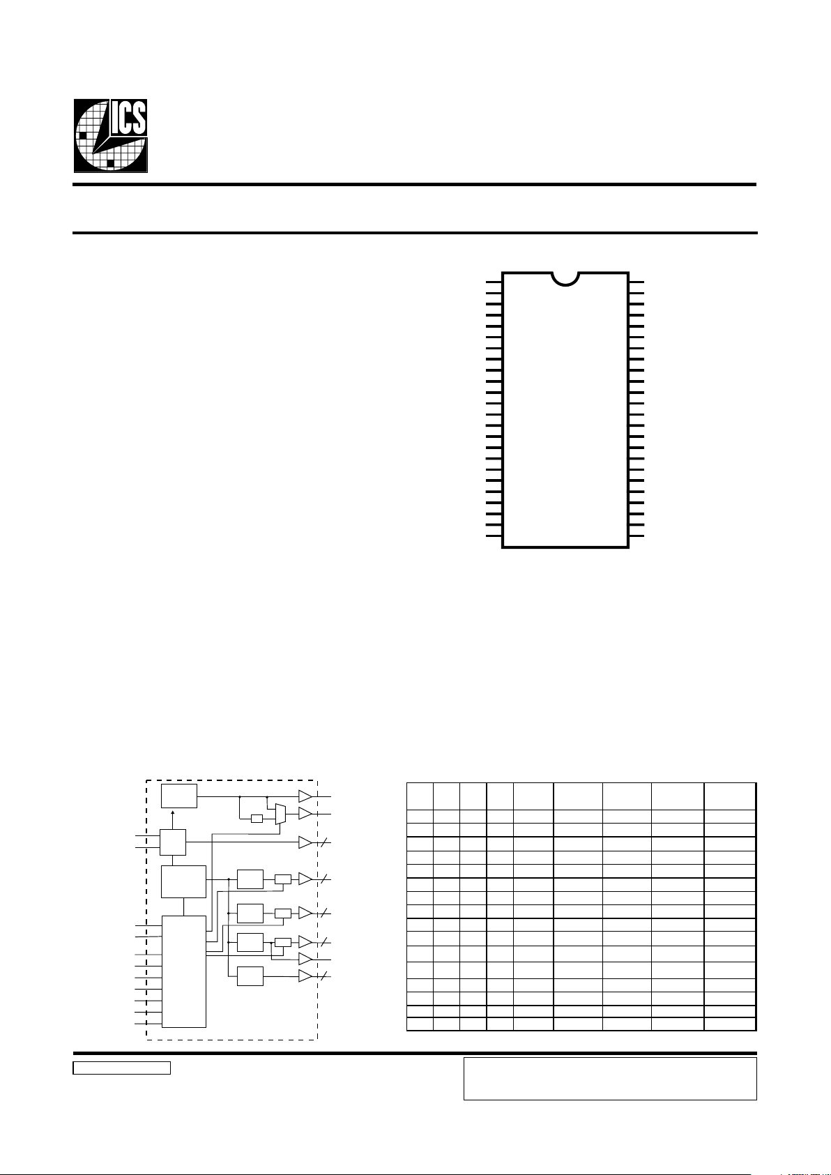
Block Diagram
Recommended Application:
Single chip clock solution 630S chipset.
Output Features:
• 3 - CPU @ 2.5V
• 13 - SDRAM @ 3.3V
• 6- PCI @3.3V,
• 2 - AGP @ 3.3V
• 1- 48MHz, @3.3V fixed.
• 1- 24/48MHz, @3.3V selectable by I
2
C
(Default is 24MHz)
• 2- REF @3.3V, 14.318MHz.
Features:
• Programmable ouput frequency.
• Programmable ouput rise/fall time.
• Programmable SDRAM and CPU skew.
• Spread spectrum for EMI control typically
by 7dB to 8dB,
with programmable spread percentage.
• Watchdog timer technology to reset system
if over-clocking causes malfunction.
• Uses external 14.318MHz crystal.
• FS pins for frequency select
Skew Specifications:
• CPU - CPU: < 175ps
• SDRAM - SDRAM < 250ps (except SDRAM12)
• PCI - PCI: < 500ps
• CPU (early) - PCI: 1-4ns (typ. 2ns)
Functionality
Pin Configuration
48-Pin 300mil SSOP
* These inputs have a 120K pull down to GND.
1
These are double strength.
PLL2
PLL1
Spread
Spectrum
48MHz
24_48MHz
CPUCLK (2:0)
SDRAM (12:0)
PCICLK (4:0)
AGP (1:0)
PCICLK_F
2
5
13
3
2
X1
X2
XTAL
OSC
CPU
DIVDER
SDRAM
DIVDER
PCI
DIVDER
Stop
Stop
Stop
S DATA
SCLK
FS(3:0)
PD#
PCI_STOP#
CPU_STOP#
SDRAM_STOP#
MODE
AGP_SEL
Control
Logic
Config.
Reg.
/ 2
REF(1:0)
AGP
DIVDER
VDDA
(AGPSEL)REF0
*(FS3)REF1
GND
X1
X2
VDDPCI
*(FS1)PCICLK_F
*(FS2)PCICLK0
PCICLK1
PCICLK2
PCICLK3
PCICLK4
GND
VDDAGP
AGPCLK0
AGPCLK1
GND
GND
*(FS0)48MHz
*(MODE)24_48MHz
VDD48
S DATA
SCLK
1
1
*
VDDL
CPUCLK0
CPUCLK1
CPUCLK2
GND
VDDSDR
SDRAM0
SDRAM1
SDRAM2
GND
SDRAM3
SDRAM4
SDRAM5
VDDSDR
SDRAM6
SDRAM7
GND
SDRAM8/PD#
SDRAM9/SDRAM_STOP#
GND
SDRAM10/PCI_STOP#
SDRAM11/CPU_STOP#
SDRAM12
VDDSDR
ICS94209
1
2
3
4
5
6
7
8
9
10
11
12
13
14
15
16
17
18
19
20
21
22
23
24
48
47
46
45
44
43
42
41
40
39
38
37
36
35
34
33
32
31
30
29
28
27
26
25
0 0 0 0 66.67 66.67 33.33 66.67 50.00
0 0 0 1 100.00 100.00 33.33 66.67 50.00
0 0 1 0 166.67 166.67 33.33 66.66 55.56
0 0 1 1 133.33 133.33 33.33 66.67 50.00
0 1 0 0 66.67 100.00 33.33 66.67 50.00
0 1 0 1 100.00 66.67 33.33 66. 67 50.00
0 1 1 0 100.00 133.33 33.33 66.67 50. 00
0 1 1 1 133.33 100.00 33.33 66.67 50. 00
1 0 0 0 112.00 112.00 33.60 67.20 56. 00
1 0 0 1 124.00 124.00 31.00 62.00 46. 50
1 0 1 0 138.00 138.00 34.50 69.00 51. 75
1 0 1 1 150.00 150.00 30.00 60.00 50. 00
1 1 0 0 66.67 133.33 33.33 66.67 50.00
1 1 0 1 100.00 150.00 30.00 60.00 50. 00
1 1 1 0 150.00 100.00 30.00 60.00 50. 00
1 1 1 1 160.00 120.00 30.00 60.00 48. 00
AGP
SEL = 0
AGP
SEL = 1
CPU SDRAM PCI C L K FS3FS2FS1FS0
ICS reserves the right to make changes in the device data identified in
this publication without further notice. ICS advises its customers to
obtain the latest version of all device data to verify that any
information being relied upon by the customer is current and accurate.

2
ICS94209
Third party brands and names are the property of their respective owners.
General Description
Pin Configuration
The ICS94209 is a single chip clock solution for desktop
designs using 630S chipsets. It provides all necessary clock
signals for such a system.
The ICS94209 belongs to ICS new generation of
programmable system clock generators. It employs serial
programming I2C interface as a vehicle for changing output
functions, changing output frequency, configuring output
strength, configuring output to output skew, changing spread
spectrum amount, changing group divider ratio and dis/
enabling individual clocks. This device also has ICS propriety
'Watchdog Timer' technology which will reset the frequency
to a safe setting if the system becomes unstable from over
clocking.
Power Groups
Analog
VDDA = X1, X2, Core, PLL
VDD48 = 48MHz, 24MHz, fixed PLL
Digital
VDDPCI = PCICLK_F , PCICLK
VDDSDR = SDRAM
VDDAGP=AGP , REF
EDOM
12niP
72niP82niP03niP13niP
011MARDS01MARDS9MARDS8MARDS
1#POTS_UPC#POTS_ICP#POTS_MARDS#DP
MODE Pin Power Management Control Input
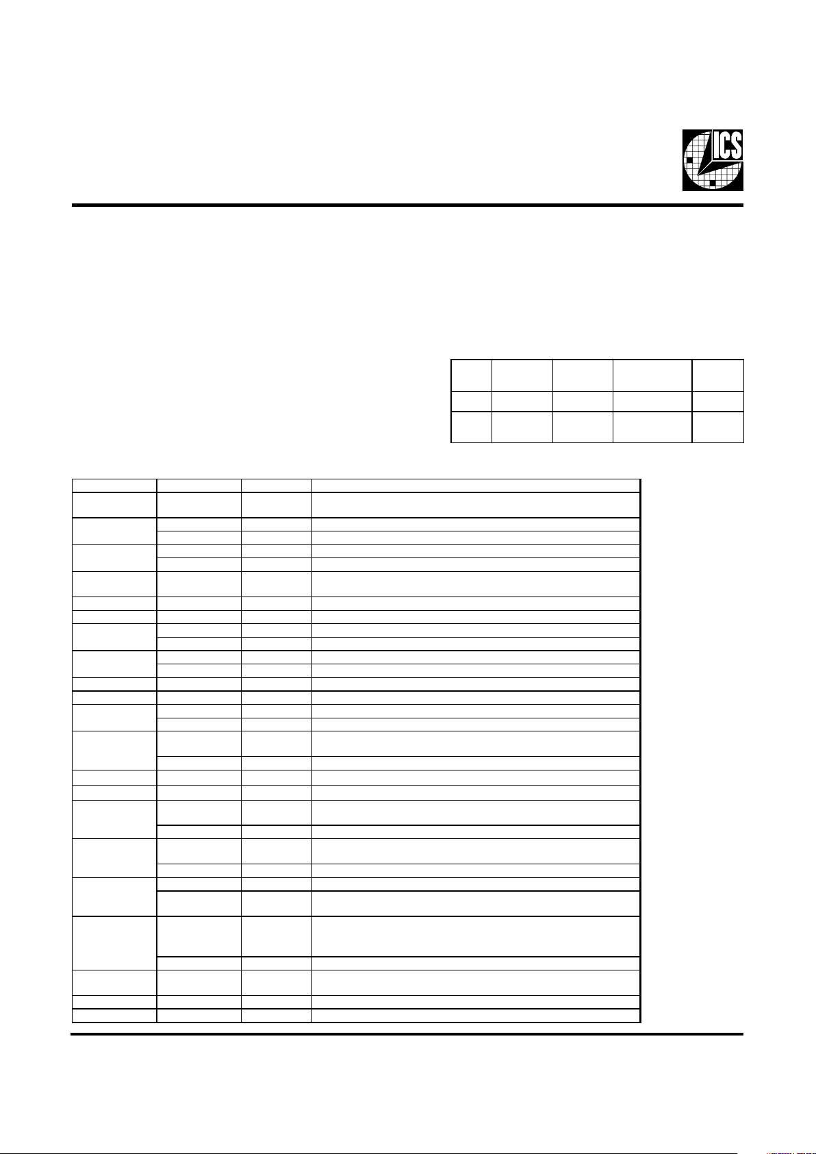
PIN NUMBER PIN NAME TYPE DESCRIPTION
1, 7, 15, 22, 25,
35, 43
VDD PWR
3.3V Pow er supply for SD RAM output buffers, PCI output buffers,
reference out
p
ut buffers and 48MH z output
AGPSEL IN AG P frequency select pin.
REF0 OUT 14.318 MHz reference clock.
FS3 IN Frequency select pin.
REF1 OUT 14.318 MHz reference clock.
4, 14, 18, 19, 29,
32, 39, 44
GN D PWR Ground pin for 3V outputs.
5 X1 IN Crystal input,nominally 14.318MHz.
6 X2 OUT Crystal output, nominally 14.318MHz.
FS1 IN Frequency select pin.
PCICLK_F OUT PCI clock output, not affected by PCI_STOP #
FS2 IN Frequency select pin.
PCICLK0 OUT PCI clock output.
13, 12, 11, 10 PCICLK (4:1) OUT PCI clock outputs.
17, 16, AGP (1:0) OUT AG P outputs defined as 2X PCI. These may not be stopped.
FS0 IN Frequency select pin.
48MH z OUT 48MH z output clock
MODE IN
Pin 27, 28, 30, & 31 function select pin
0=Deskto
p
1=Mobile mode
24_48MH z OUT Clock output for super I/O/USB default is 24MHz
23 SDATA I/O
Data
p
in for I2C circuitry 5V tolerant
24 SCLK IN
Clock
p
in of I2C circuitry 5V tolerant
CPU_STOP# IN
Stops all PCICLKs besides the PCICLK_F clocks at logic 0 level, when input
is low and M ODE
p
in is in M ob ile mode
SDRAM11 OUT SDRAM clock output
PCI_STOP# IN
Stops all CPU CLKs clocks at logic 0 level, when input is low and MODE pin
is in M obile mode
SDRAM10 OUT SDRAM clock output
SDR AM 9 OU T SD RAM clock output
SDRAM_STOP# IN
Stops all SDRAM clocks at logic 0 level, when input is low and MO DE pin
is in M obile mode
PD# IN
Asynchronous active low input pin used to power down the device into a low
pow er state. The internal clocks are disabled and the VCO and the crys tal are
stopped. The latency of the power down w ill not be greater than 3ms.
SDR AM 8 OU T SD RAM clock output
26 33, 34, 36, 37,
38, 40, 41, 42
SDRAM (12, 7:0) OUT SDRAM clock outputs
45, 46, 47 CPUCLK (2:0) OUT CPU clock outputs.
48 VD DL PWR Pow er pin for the CPU CLKs. 2.5V
31
20
2
8
9
21
3
30
27
28

3
ICS94209
Third party brands and names are the property of their respective owners.
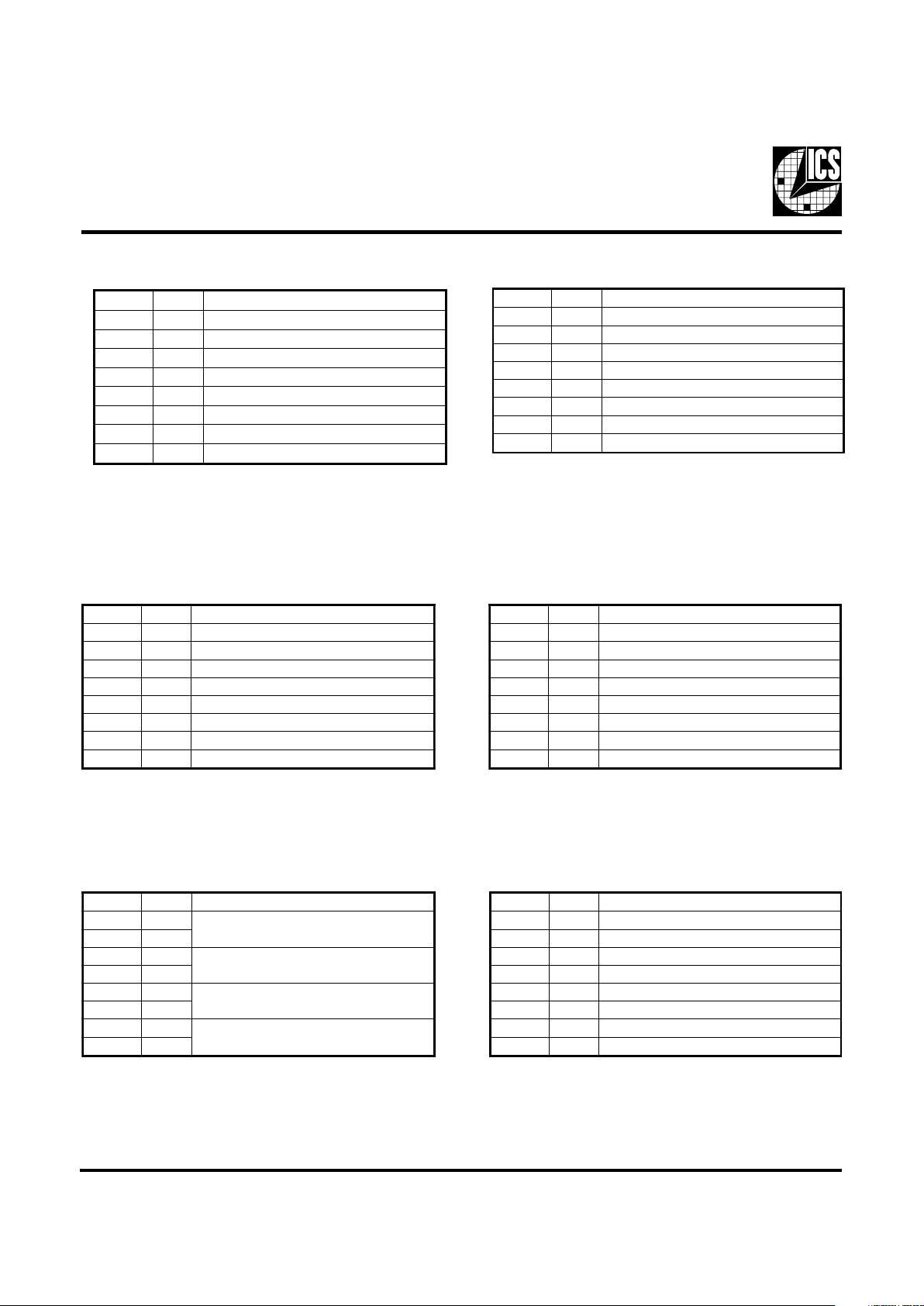
Byte0: Functionality and Frequency Select Register (default = 0)
Serial Configuration Command Bitmap
Note: PWD = Power-Up Default
Note1:
Default at power-up will be for latched logic inputs to define frequency, as displayed by Bit 3.
I
2
C is a trademark of Philips Corporation
tiBnoitpircseDDWP
2tiB
4:7tiB
2tiB
7tiB6tiB5tiB4tiB
00000
1etoN
3SF2SF1SF0SFUPCMARDSICP
PGA
0=LES
PGA
1=LES
egatnecerPdaerpS
0000 0 76.6676.6633.3376.6600.05daerpSnwoD%5.0-ot0
0000 1 00.00100.00133.3376.6600.05daerpSnwoD%5.0-ot0
000 10 76.66176.66133.3366.6665.55daerpSretneC%52.0-/+
000 1 1 33.33133.33133.3376.6600.05daerpSnwoD%5.0-ot0
0010 0 76.6600.00133.3376.6600.05daerpSnwoD%5.0-ot0
0010 1 00.00176.6633.3376.6600.05daerpSnwoD%5.0-ot0
00110 00.00133.33133.3376.6600.05daerpSnwoD%5.0-ot0
0011 1 33.33100.00133.3376.6600.05daerpSnwoD%5.0-ot0
01000 00.21100.21106.3302.7600.65daerpSretneC%52.0-/+
0100 1 00.42100.42100.1300.2605.64daerpSretneC%52.0-/+
01010 00.83100.83105.4300.9657.15daerpSretneC%52.0-/+
0101 1 00.05100.05100.0300.0600.05daerpSretneC%52.0-/+
01100 76.6633.33133.3376.6600.05daerpSnwoD%5.0-ot0
0110 1 00.00100.05100.0300.0600.05daerpSretneC%52.0-/+
01110 00.05100.00100.0300.0600.05daerpSretneC%52.0-/+
0111 1 00.06100.02100.0300.0600.84daerpSretneC%52.0-/+
1000 0 00.30100.30133.4376.8600.05daerpSretneC%52.0-/+
1000 1 03.00103.00134.3378.6600.05daerpSretneC%52.0-/+
100 1 0 00.00200.00233.3376.6600.05daerpSretneC%52.0-/+
100 1 1 37.33137.33134.3378.6651.05daerpSretneC%52.0-/+
1010 0 00.30133.73133.4376.8605.15daerpSretneC%52.0-/+
1010 1 33.73100.30133.4376.8605.15daerpSretneC%52.0-/+
101 1 0 78.6603.00134.3378.6651.05daerpSretneC%52.0-/+
101 1 1 37.33103.00134.3378.6651.05daerpSretneC%52.0-/+
1100 0 00.01100.01100.3300.6600.55daerpSretneC%52.0-/+
1100 1 00.51100.51105.4300.9605.75daerpSretneC%52.0-/+
110 10 00.04100.04100.5300.0705.25daerpSretneC%52.0-/+
110 1 1 05.10105.10138.3376.7600.05daerpSretneC%52.0-/+
1110 0 03.00137.33134.3378.6651.05daerpSretneC%52.0-/+
1110 1 00.50100.04100.5300.0705.25daerpSretneC%52.0-/+
11110 00.50105.75105.1300.3605.25daerpSretneC%52.0-/+
1111 1 33.53105.10138.3376.7657.05daerpSretneC%52.0-/+
3tiB
stupnIdehctaL,tceleserawdrahybdetcelessiycneuqerF-0
4:72,tiBybdetcelessiycneuqerF-1
0
1tiB
lamroN-0
delbanEmurtcepSdaerpS-1
1
0tiB
gninnuR-0
stuptuollaetatsirT-1
0

4
ICS94209
Third party brands and names are the property of their respective owners.
Byte 1: CPU, Active/Inactive Register
(1= enable, 0 = disable)
Byte 2: PCI, Active/Inactive Register
(1= enable, 0 = disable)
TIB#NIPDWPNOITPIRCSED
7tiB-1 devreseR
6tiB-1 devreseR
5tiB311 4KLCICP
4tiB211 3KLCICP
3tiB111 2KLCICP
2tiB011 1KLCICP
1tiB91 0KLCICP
0tiB81 F_KLCICP
Notes:
1. Inactive means outputs are held LOW and are disabled
from switching.
2. Latched Frequency Selects (FS#) will be inverted logic
load of the input frequency select pin conditions.
TIB#NIPDWPNOITPIRCSED
7tiB-1 devreseR
6tiB121 zHM84_42
5tiB021 zHM84
4tiB621 21MARDS
3tiB721 11MARDS
2tiB821 01MARDS
1tiB031 9MARDS
0tiB131 8MARDS
Byte 4: SDRAM , Active/Inactive Register
(1= enable, 0 = disable)
TIB#NIPDWPNOITPIRCSED
7tiB-X )kcabdaeR(3SF
6tiB-X )kcabdaeR(2SF
5tiB-X )kcabdaeR(1SF
4tiB-X )kcabdaeR(0SF
3tiB310FER
2tiB211FER
1tiB711 1KLCPGA
0tiB611 0KLCPGA
Byte 5: AGP, Active/Inactive Register
(1= enable, 0 = disable)
Byte 3: SDRAM, Active/Inactive Register
(1= enable, 0 = disable)
TIB#NIPDWPNOITPIRCSED
7tiB331 7MARDS
6tiB431 6MARDS
5tiB631 5MARDS
4tiB731 4MARDS
3tiB831 3MARDS
2tiB041 2MARDS
1tiB141 1MARDS
0tiB241 0MARDS
TIB#NIPDWPNOITPIRCSED
7tiB-1
84_42leS
)zHM84:0,zHM42:1(
6tiB-1 devreseR
5tiB-1 devreseR
4tiB-1 devreseR
3tiB741 0KLCUPC
2tiB641 1KLCUPC
1tiB541 2KLCUPC
0tiB-1 devreseR

5
ICS94209
Third party brands and names are the property of their respective owners.
Byte 6: Control , Active/Inactive Register
(1= enable, 0 = disable)
TIB#NIPDWPNOITPIRCSED
7tiB-0 devreseR
6tiB-0 devreseR
5tiB-1 devreseR
4tiB-0 devreseR
3tiB-1 devreseR
2tiB-0 devreseR
1tiB-0 devreseR
0tiB-1 devreseR
Byte 7: Vendor ID Register
(1= enable, 0 = disable)
TIB#NIPDWPNOITPIRCSED
7tiB3,20 X2=1,X1=0htgnertsFER
6tiB540
lortnoC-potS-2KLCUPC
,2KLCUPClortnoclliw#POTS_UPC=0
wolsi#POTS_UPCfinevegninnureerfsi2KLCUPC=1
5tiB-X )kcabdaeR(LESPGA
4tiB-X )kcabdaeR(EDOM
3tiB-X )kcabdaeR(#POTS_UPC
2tiB-X )kcabdaeR(#POTS_ICP
1tiB-X )kcabdaeR(#POTS_MARDS
0tiB-0
elggoTdeepSPGA
,gnittestupnihctalybdenimretedeblliw)2nip(LESPGA=0
gnittestupnihctalfoetisoppoeblliwLESPGA=1
Byte 8: Byte Count and Read Back Register
(1= enable, 0 = disable)
TIB#NIPDWPNOITPIRCSED
7tiB-0 devreseR
6tiB-0 devreseR
5tiB-0 devreseR
4tiB-0 devreseR
3tiB-0 devreseR
2tiB-1 devreseR
1tiB-0 devreseR
0tiB-0 devreseR
Note: FS values in bit [0:4] will correspond to Byte 0 FS
values. Default safe frequency is same as 00000 entry in
byte0.
Byte 10: VCO Control Selection Bit &
Watchdog Timer Control Register
tiBDWPnoitpircseD
7tiB0 qerf21&11B=1/qerf0B/wH=0
6tiB0 elbane=1/elbasid=0elbanEDW
5tiB0 mrala=1/lamron=0sutatSDW
4tiB0 2tib0etyB,ycneuqerFefaSDW
3tiB0 3SF,ycneuqerFefaSDW
2tiB0 2SF,ycneuqerFefaSDW
1tiB0 1SF,ycneuqerFefaSDW
0tiB0 0SF,ycneuqerFefaSDW
Byte 9: Watchdog Timer Count Register
tiBDWPnoitpircseD
7tiB0
esehtfonoitatneserperlamicedehT
sm1rosm092otdnopserrocstib8
erofebtiawlliwremitgodhctaweht
ehtteserdnaedommralaotseogti
tluafeD.gnittesefasehtotycneuqerf
6.4=sm092X61sipurewopta
.sdnoces
6tiB0
5tiB0
4tiB1
3tiB0
2tiB0
1tiB0
0tiB0

6
ICS94209
Third party brands and names are the property of their respective owners.
Notes:
1. PWD = Power on Default
Byte 11: VCO Frequency Control Register
Note: The decimal representation of these 7 bits (Byte 11
[6:0]) + 2 is equal to the REF divider value .
tiBDWPnoitpircseD
7tiBX 0tiBrediviDOCV
6tiBX 6tiBrediviDFER
5tiBX 5tiBrediviDFER
4tiBX 4tiBrediviDFER
3tiBX 3tiBrediviDFER
2tiBX 2tiBrediviDFER
1tiBX 1tiBrediviDFER
0tiBX 0tiBrediviDFER
Byte 12: VCO Frequency Control Register
Note: The decimal representation of these 9 bits (Byte 12
bit [7:0] & Byte 11 bit [7] ) + 8 is equal to the VCO divider
value. For example if VCO divider value of 36 is desired,
user need to program 36 - 8 = 28, namely, 0, 00011100 into
byte 12 bit & byte 11 bit 7.
tiBDWPnoitpircseD
7tiBX 8tiBrediviDOCV
6tiBX 7tiBrediviDOCV
5tiBX 6tiBrediviDOCV
4tiBX 5tiBrediviDOCV
3tiBX 4tiBrediviDOCV
2tiBX 3tiBrediviDOCV
1tiBX 2tiBrediviDOCV
0tiBX 1tiBrediviDOCV
Byte 13: Spread Sectrum Control Register Byte 14: Spread Sectrum Control Register
Note: Please utilize software utility provided by ICS
Application Engineering to configure spread spectrum.
Incorrect spread percentage may cause system failure.
tiBDWPnoitpircseD
7tiBX 7tiBmurtcepSdaerpS
6tiBX 6tiBmurtcepSdaerpS
5tiBX 5tiBmurtcepSdaerpS
4tiBX 4tiBmurtcepSdaerpS
3tiBX 3tiBmurtcepSdaerpS
2tiBX 2tiBmurtcepSdaerpS
1tiBX 1tiBmurtcepSdaerpS
0tiBX 0tiBmurtcepSdaerpS
tiBDWPnoitpircseD
7tiBX devreseR
6tiBX devreseR
5tiBX devreseR
4tiBX 21tiBmurtcepSdaerpS
3tiBX 11tiBmurtcepSdaerpS
2tiBX 01tiBmurtcepSdaerpS
1tiBX 9iBmurtcepSdaerpS
0tiBX 8tiBmurtcepSdaerpS
Note: Please utilize software utility provided by ICS
Application Engineering to configure spread spectrum.
Incorrect spread percentage may cause system failure.
Byte 15: Output Skew Control
Byte 16: Output Skew Control
tiBDWPnoitpircseD
7tiB1
lortnoCwekS21MARDS
6tiB0
5tiB0
lortnoCwekS)0:11(MARDS
4tiB1
3tiB1
lortnoCwekS2KLCUPC
2tiB1
1tiB1
lortnoCwekS)0:1(KLCUPC
0tiB0
tiBDWPnoitpircseD
7tiBX devreseR
6tiBX devreseR
5tiBX devreseR
4tiBX devreseR
3tiBX devreseR
2tiBX devreseR
1tiBX devreseR
0tiBX devreseR
 Loading...